capacitor that shifts a waveform to a different dc level ...ee.eng.usm.my/eeacad/arjuna/electronic...
TRANSCRIPT
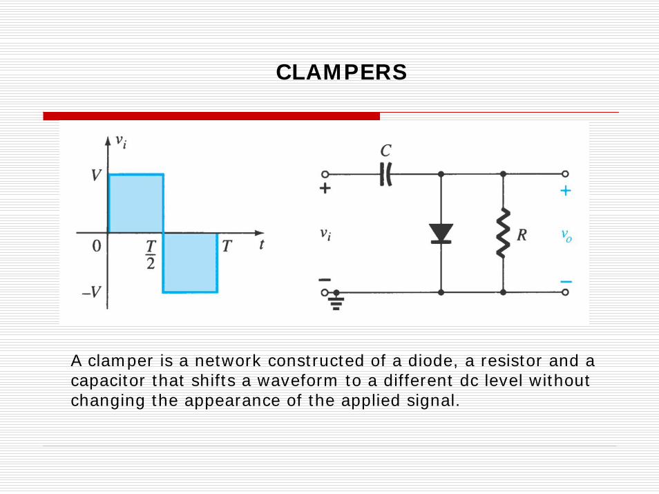
CLAMPERS
A clamper is a network constructed of a diode, a resistor and a capacitor that shifts a waveform to a different dc level withoutchanging the appearance of the applied signal.
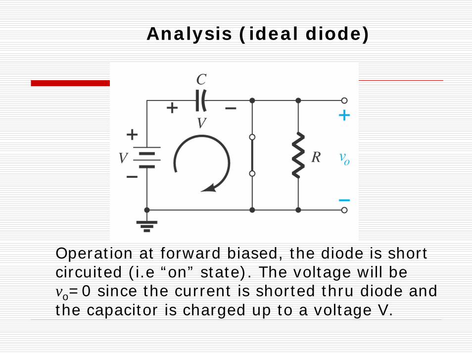
Operation at forward biased, the diode is short circuited (i.e “on” state). The voltage will be vo=0 since the current is shorted thru diode and the capacitor is charged up to a voltage V.
Analysis (ideal diode)
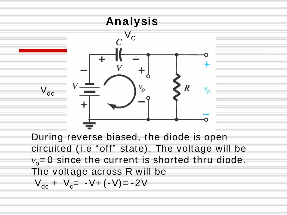
Analysis
During reverse biased, the diode is open circuited (i.e “off” state). The voltage will be vo=0 since the current is shorted thru diode. The voltage across R will beVdc + Vc= -V+(-V)=-2V
Vdc
VC
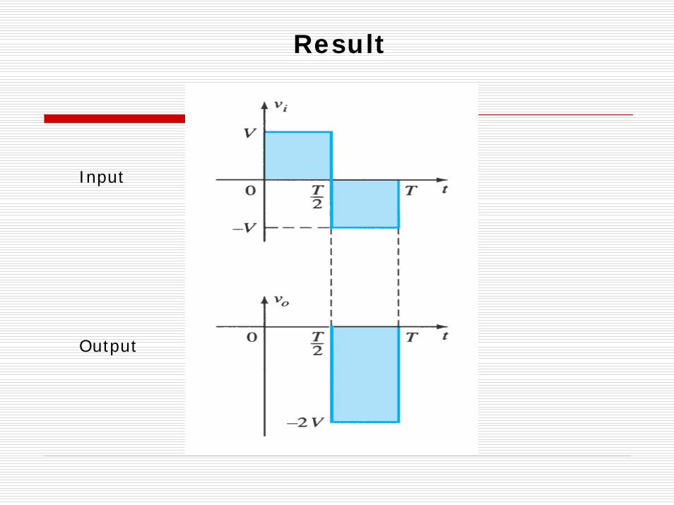
Result
Input
Output
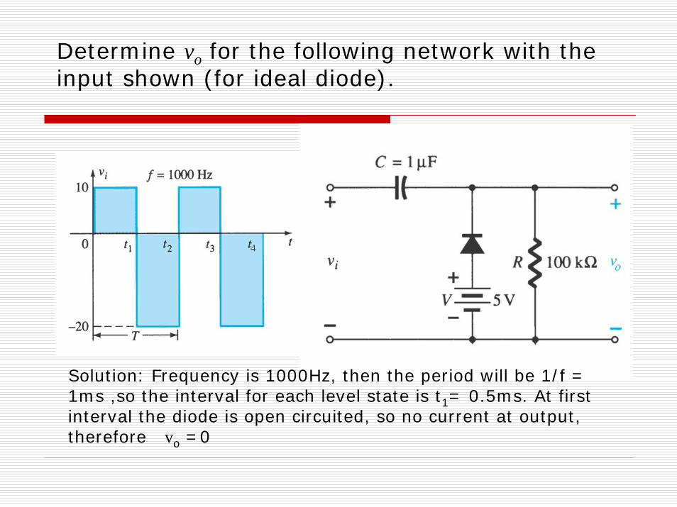
Determine vo for the following network with the input shown (for ideal diode).
Solution: Frequency is 1000Hz, then the period will be 1/f = 1ms ,so the interval for each level state is t1= 0.5ms. At first interval the diode is open circuited, so no current at output, therefore vo =0

Analysis (forward biased)
At 2nd interval, the diode is short circuited, the voltage across R will be the same as across the batery (parallel) Vo= 5VThe voltage that charge up the capacitor, Applying KVL
-20V +Vc -5V =0 , then VC=25V
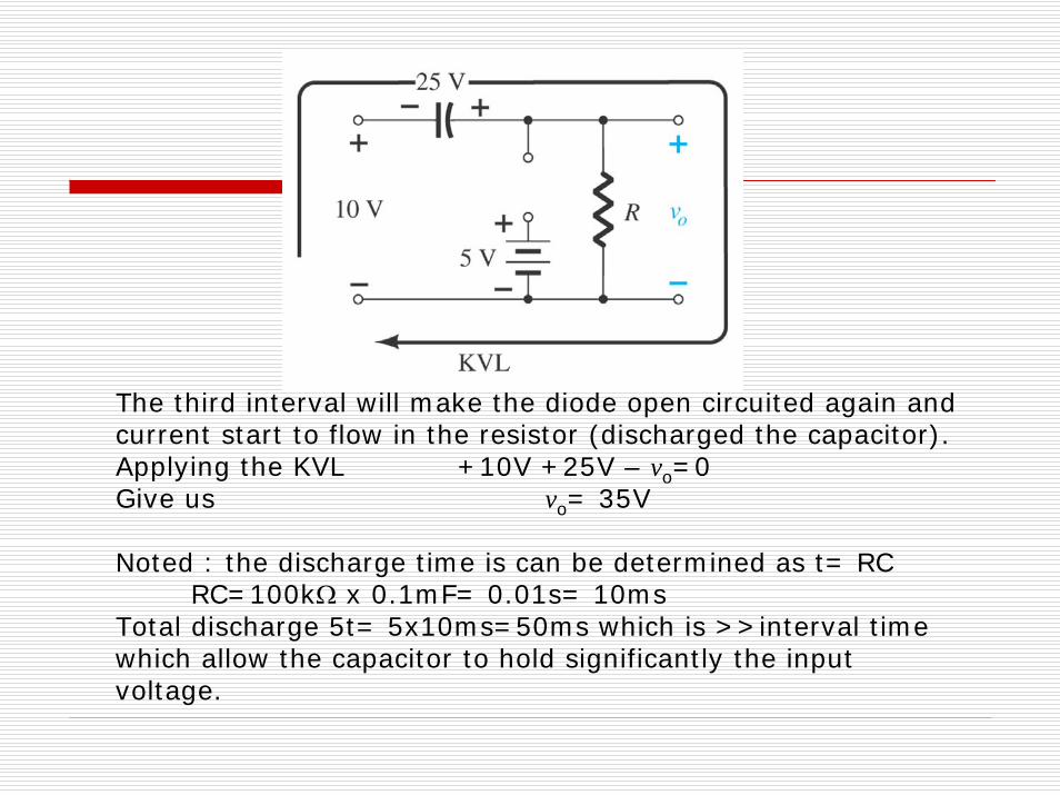
The third interval will make the diode open circuited again and current start to flow in the resistor (discharged the capacitor). Applying the KVL +10V +25V – vo=0Give us vo= 35V
Noted : the discharge time is can be determined as t= RCRC=100kΩ x 0.1mF= 0.01s= 10ms
Total discharge 5t= 5x10ms=50ms which is >>interval time which allow the capacitor to hold significantly the input voltage.
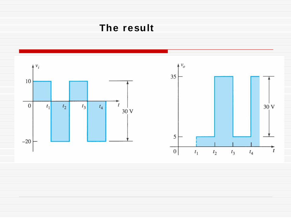
The result
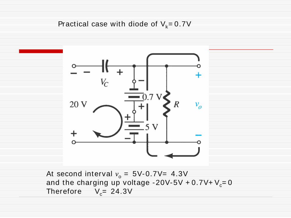
Practical case with diode of Vk=0.7V
At second interval vo = 5V-0.7V= 4.3V and the charging up voltage -20V-5V +0.7V+Vc=0Therefore Vc= 24.3V

The third interval we have10V+24.3V-vo=0Thus vo= 34.3V
Circuit
result
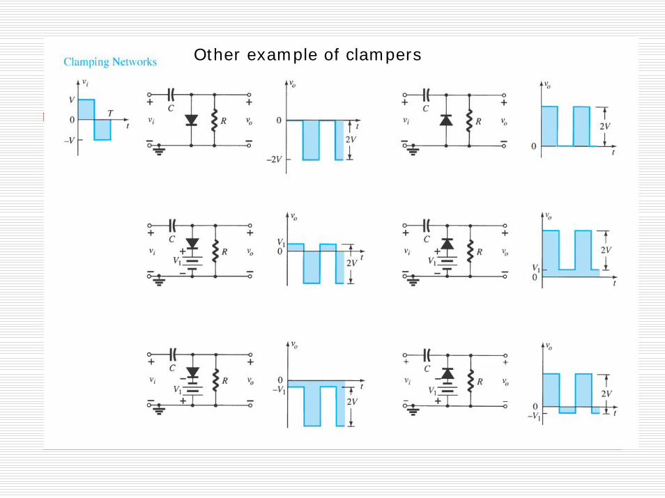
Other example of clampers
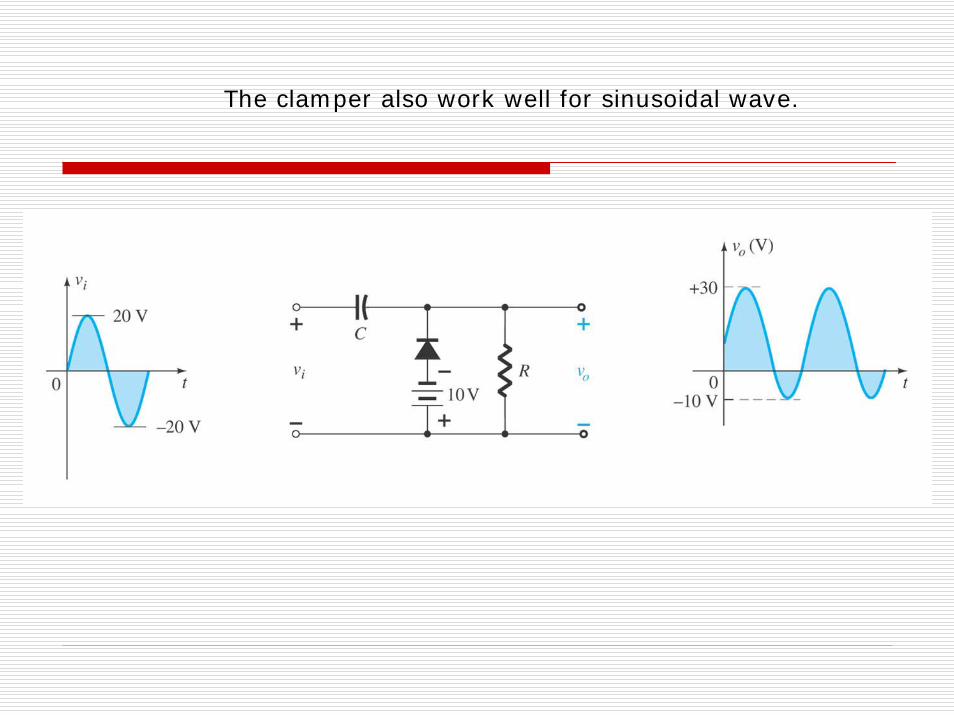
The clamper also work well for sinusoidal wave.
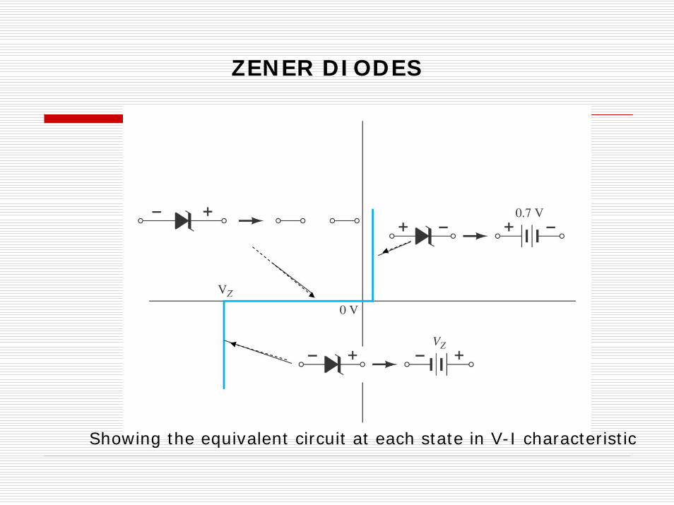
ZENER DIODES
Showing the equivalent circuit at each state in V-I characteristic
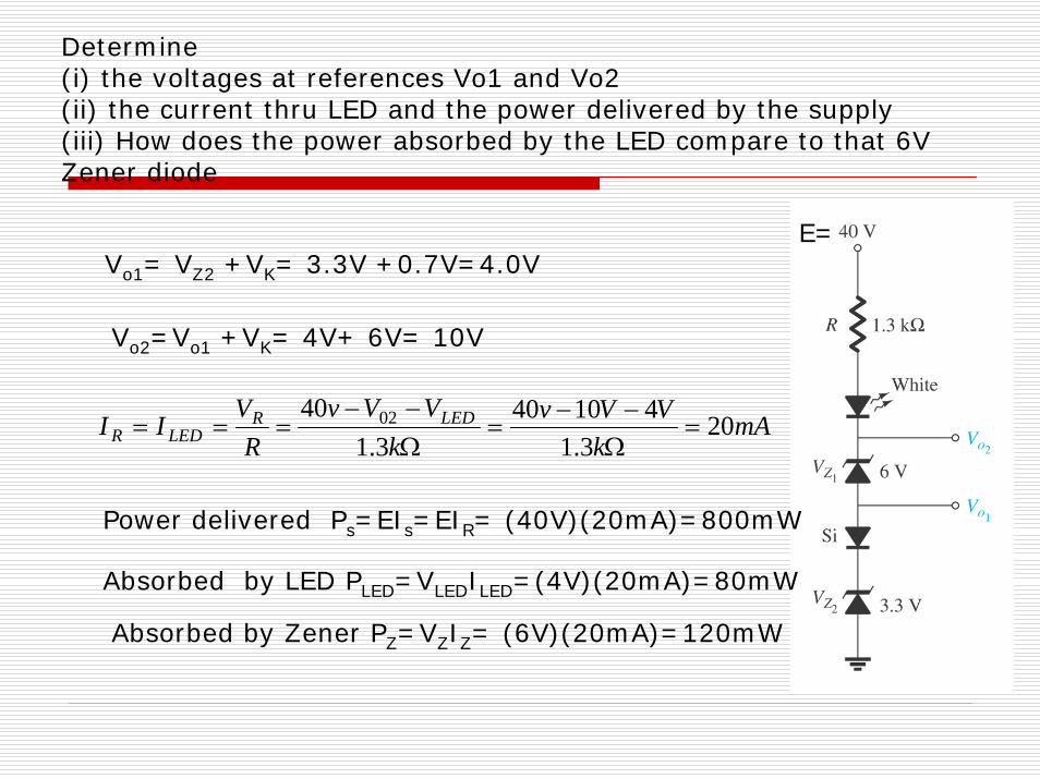
Determine (i) the voltages at references Vo1 and Vo2 (ii) the current thru LED and the power delivered by the supply(iii) How does the power absorbed by the LED compare to that 6V Zener diode
Vo1= VZ2 +VK= 3.3V +0.7V=4.0V
Vo2=Vo1 +VK= 4V+ 6V= 10V
mAk
VVvk
VVvR
VII LEDRLEDR 20
3.141040
3.140 02 =
Ω−−
=Ω−−
===
Power delivered Ps=EIs=EIR= (40V)(20mA)=800mW
E=
Absorbed by LED PLED=VLEDILED=(4V)(20mA)=80mW
Absorbed by Zener PZ=VZIZ= (6V)(20mA)=120mW

A LIMITER
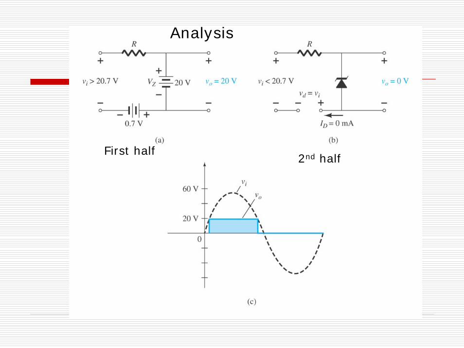
Analysis
First half2nd half
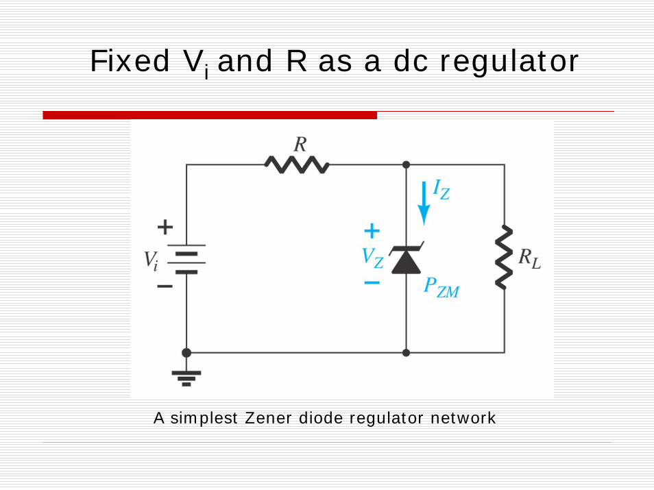
Fixed Vi and R as a dc regulator
A simplest Zener diode regulator network
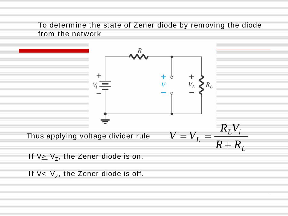
To determine the state of Zener diode by removing the diode from the network
Thus applying voltage divider rule
L
iLL RR
VRVV
+==
If V> VZ, the Zener diode is on.
If V< VZ, the Zener diode is off.

Zener equivalent for the “on” situation
Since Zener is directly parallel to RL , then VL=VZ
Zener current , applying Kirchoff’s current law IR = IZ + IL
Thus IZ = IR – IL
And Power PZ= VZ IZ
L
LL R
VI =RVV
RV
I LiRR
−==
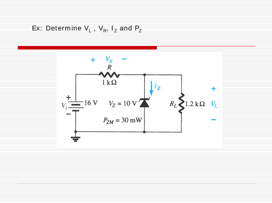
Ex: Determine VL , VR, IZ and PZ
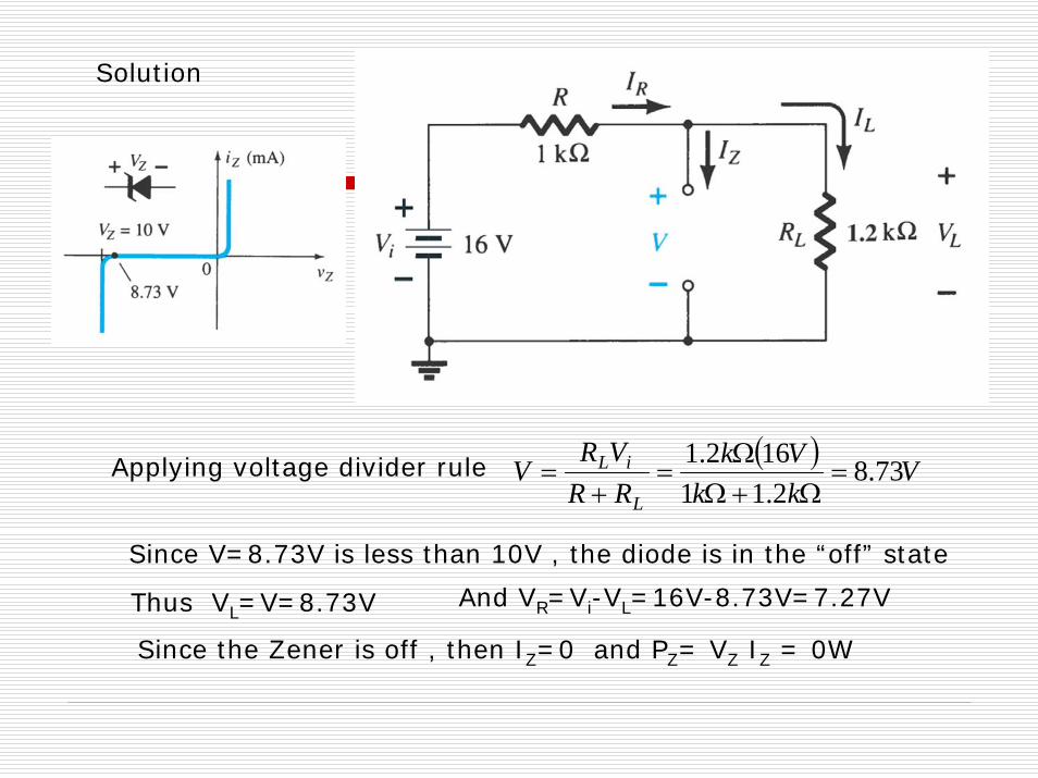
Solution
( ) VkkVk
RRVR
VL
iL 73.82.11
162.1=
Ω+ΩΩ
=+
=Applying voltage divider rule
Since V=8.73V is less than 10V , the diode is in the “off” state
Thus VL=V=8.73V And VR=Vi-VL=16V-8.73V=7.27V
Since the Zener is off , then IZ=0 and PZ= VZ IZ = 0W
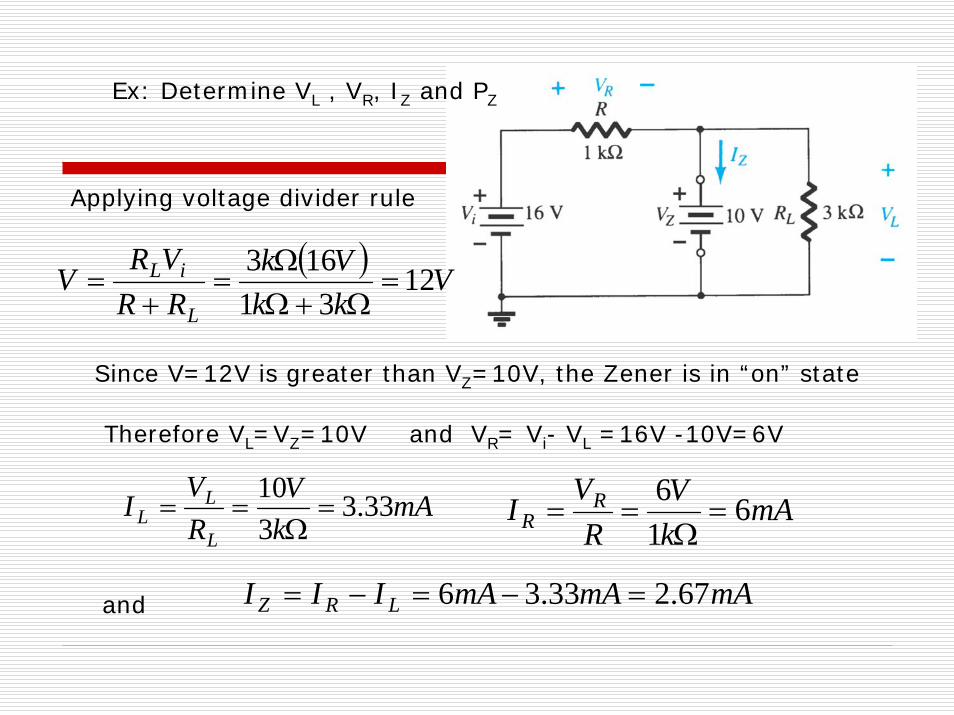
Ex: Determine VL , VR, IZ and PZ
( ) VkkVk
RRVR
VL
iL 1231
163=
Ω+ΩΩ
=+
=
mAmAmAIII LRZ 67.233.36 =−=−=
mAkV
RVI
L
LL 33.3
310
=Ω
==
Applying voltage divider rule
Since V=12V is greater than VZ=10V, the Zener is in “on” state
Therefore VL=VZ=10V and VR= Vi- VL =16V -10V=6V
mAkV
RVI R
R 616
=Ω
==
and
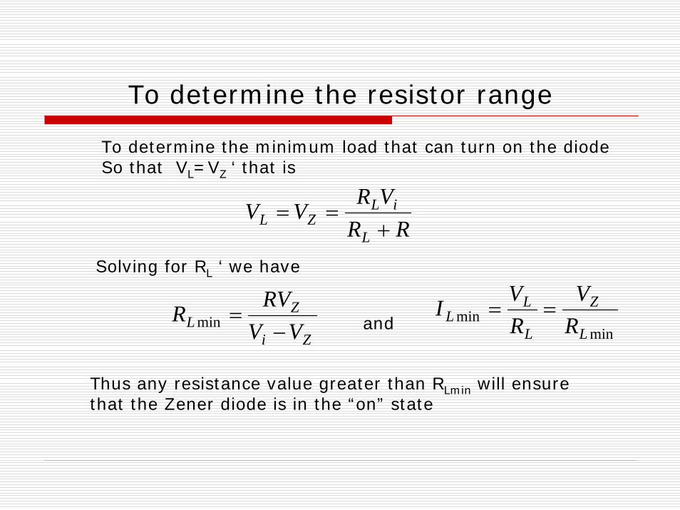
To determine the resistor range
Zi
ZL VV
RVR
−=min
RRVR
VVL
iLZL +==
minmin
L
Z
L
LL R
VRVI ==
To determine the minimum load that can turn on the diodeSo that VL=VZ ‘ that is
Solving for RL ‘ we have
and
Thus any resistance value greater than RLmin will ensure that the Zener diode is in the “on” state

To determine the resistor range
RVI R
R =
minmin
L
ZL I
VR =
Once the diode is in the “on” state, the voltage across R remains fixed at
VR= Vi - VZ
And IR remains fixed at
The Zener current IZ = IR - IL
But the IZ is limited by the manufacturer IZM , then
ILmin = IR - IZM
And the maximum load resistance as
mAkV
RVI R
R 40140
=Ω
==
( )( )Ω=
Ω=
−Ω
=−
= 25040
101050101
mink
VVVk
VVRV
RZi
ZL
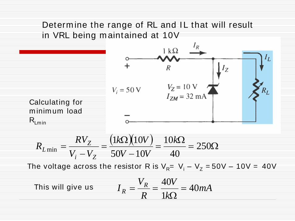
The voltage across the resistor R is VR= Vi – VZ =50V – 10V = 40V
Determine the range of RL and IL that will result in VRL being maintained at 10V
Calculating for minimum load RLmin
This will give us
Ω=== kmAV
IV
RL
ZL 25.1
810
minmax
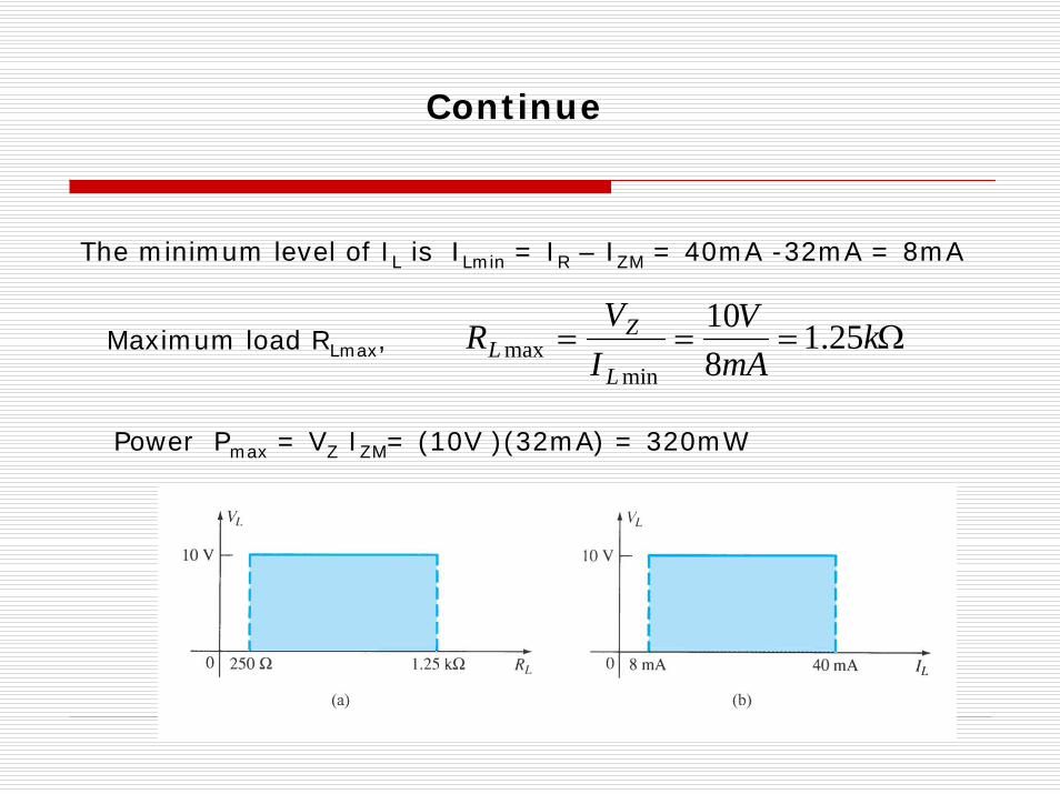
The minimum level of IL is ILmin = IR – IZM = 40mA -32mA = 8mA
Maximum load RLmax,
Continue
Power Pmax = VZ IZM= (10V )(32mA) = 320mW

Fixed RL and Variable Vi
RRVR
VVL
iLZL +==
( )L
ZLi R
VRRV
+=min
ZRi VVV += maxmax ZRi VRIV += maxmax
The voltage Vi must be sufficiently large to turn the Zener diode on. The minimum turn on voltage Vi= Vimin is
therefore
Since the maximum Zener current IZM, Thus IZM=IR-IL
Then IRMAX = IZM + IL
The maximum voltage
or

Determine the range of values of Vi that will maintain the Zener diode of in the “on” state.
( ) ( )( ) VVR
VRRVL
ZLi 67.23
1200202201200
min =ΩΩ+Ω
=+
=
mAkV
RV
RV
IL
Z
L
LL 67.16
2.120
=Ω
===
ZRi VRIV += maxmax
Using the formula given before
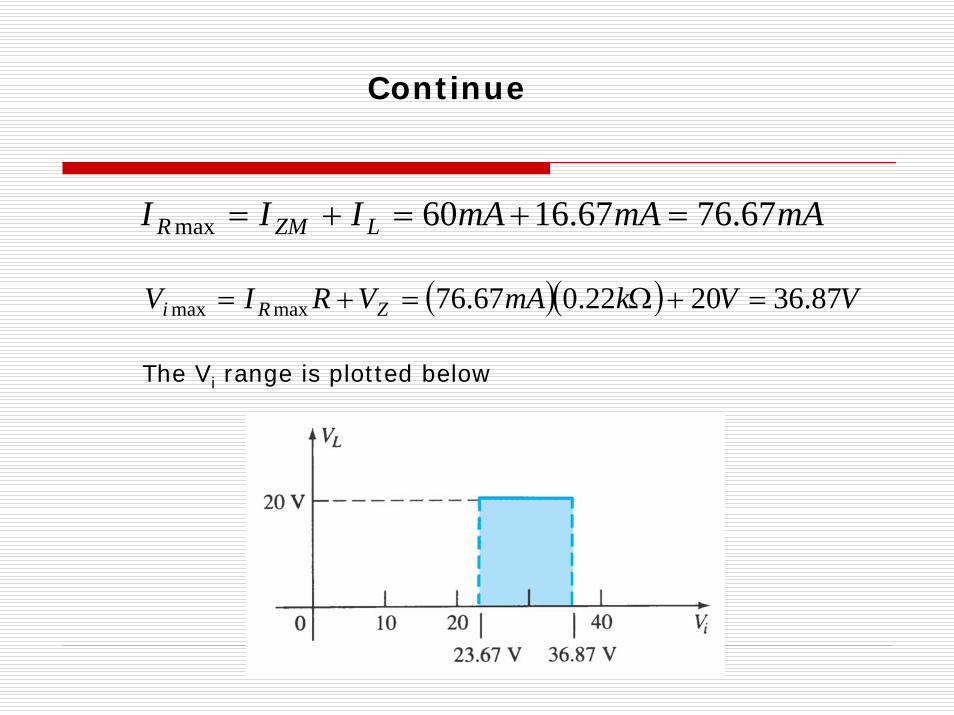
mAmAmAIII LZMR 67.7667.1660max =+=+=
( )( ) VVkmAVRIV ZRi 87.362022.067.76maxmax =+Ω=+=
Continue
The Vi range is plotted below

If the input is a ripple from full-wave rectified and filtering as shown, as long as within the specified voltage, the output will still remain constant at 20V.

Voltage Multiplier
HALF-WAVE VOLTAGE DOUBLER
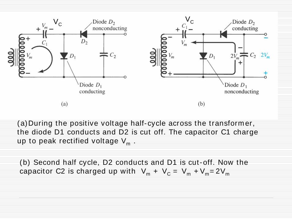
(b) Second half cycle, D2 conducts and D1 is cut-off. Now the capacitor C2 is charged up with Vm + VC = Vm +Vm=2Vm
(a)During the positive voltage half-cycle across the transformer, the diode D1 conducts and D2 is cut off. The capacitor C1 chargeup to peak rectified voltage Vm .
VCVC

FULL-WAVE VOLTAGE DOUBLER
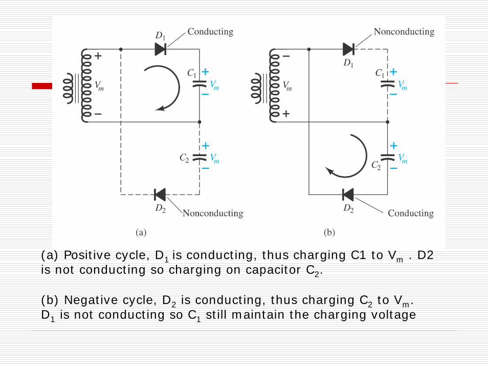
(a) Positive cycle, D1 is conducting, thus charging C1 to Vm . D2 is not conducting so charging on capacitor C2.
(b) Negative cycle, D2 is conducting, thus charging C2 to Vm. D1 is not conducting so C1 still maintain the charging voltage
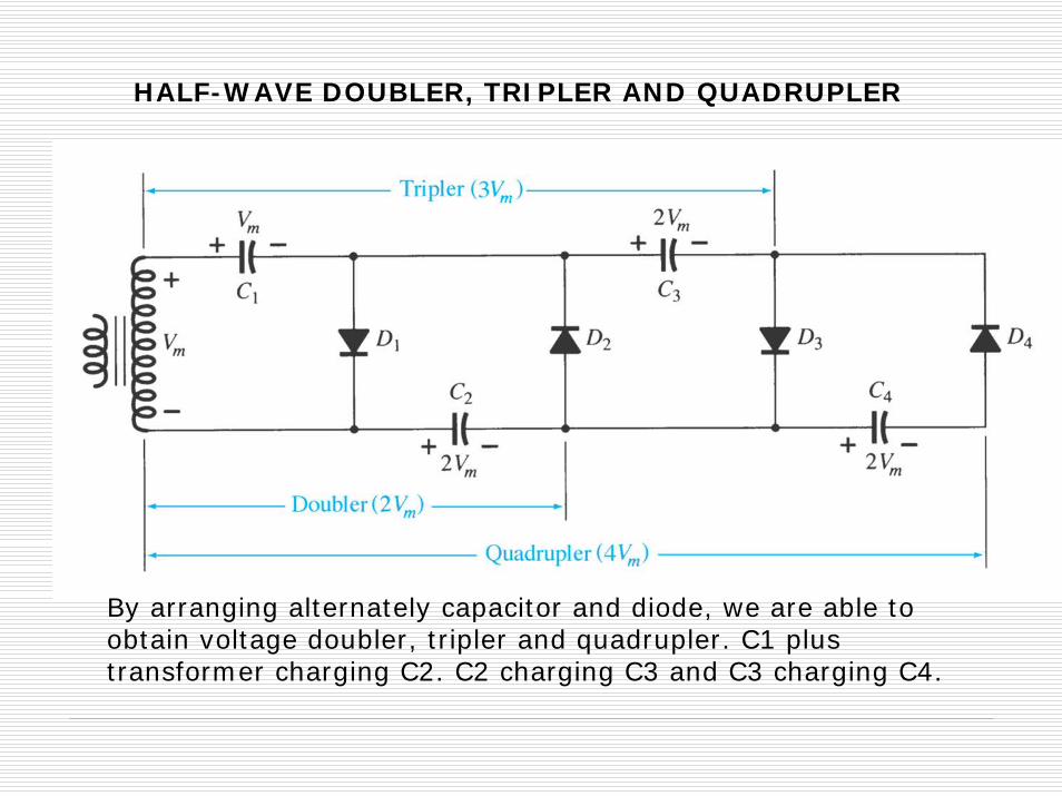
HALF-WAVE DOUBLER, TRIPLER AND QUADRUPLER
By arranging alternately capacitor and diode, we are able to obtain voltage doubler, tripler and quadrupler. C1 plus transformer charging C2. C2 charging C3 and C3 charging C4.

Protective configuration
Trying to change the current through an inductive element too quickly may result in an inductive kick that could damage surrounding elements or the system itself
Transient phase of a simple RL cct Arcing during opening the switch
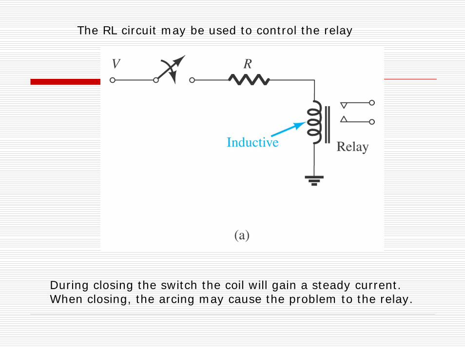
The RL circuit may be used to control the relay
During closing the switch the coil will gain a steady current. When closing, the arcing may cause the problem to the relay.
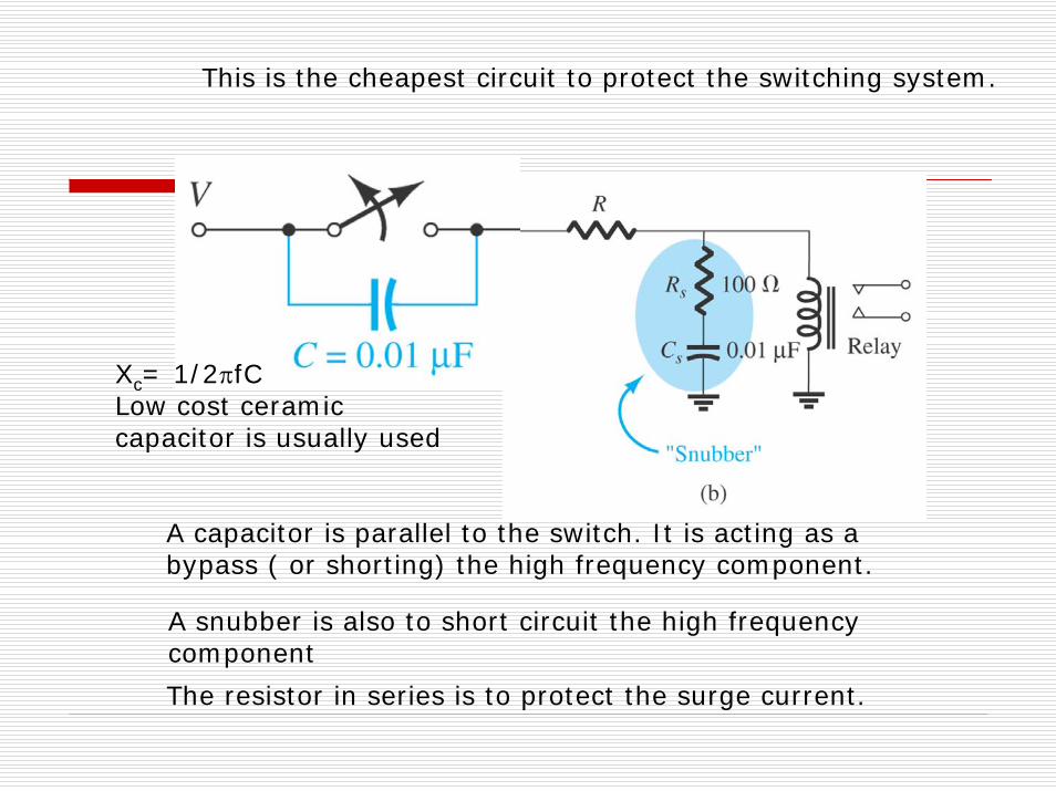
This is the cheapest circuit to protect the switching system.
A capacitor is parallel to the switch. It is acting as a bypass ( or shorting) the high frequency component.
Xc= 1/2πfCLow cost ceramic capacitor is usually used
A snubber is also to short circuit the high frequency component
The resistor in series is to protect the surge current.

Diode protection for RL circuit
A diode is placed parallel to the inductive element (relay). When switch open the polarity of voltage across coil will turn on the diode thus provide conduction path for the inductor. The diode must has the same current level to that current passing the coil

Diode protector to limit the emitter –base voltage
VBE is limited to 0.7V (knee voltage of the silicon diode)

Diode protection to prevent a reversal in collection current
A current from B to C will be blocked by the diode
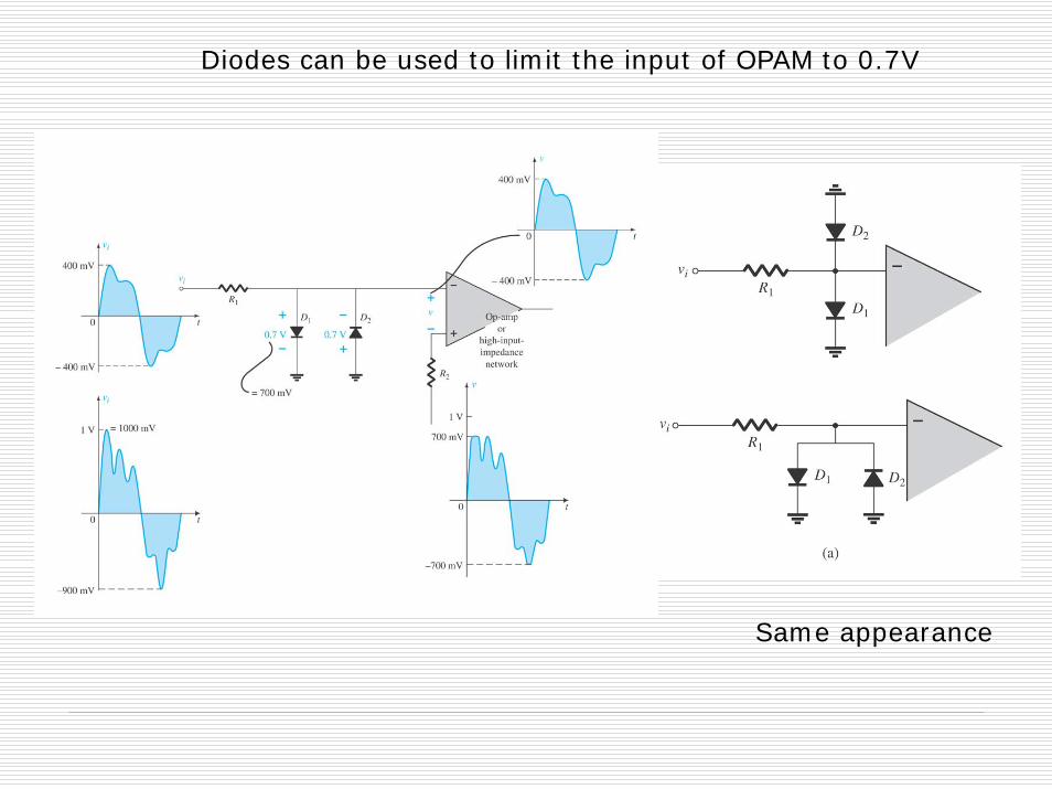
Diodes can be used to limit the input of OPAM to 0.7V
Same appearance
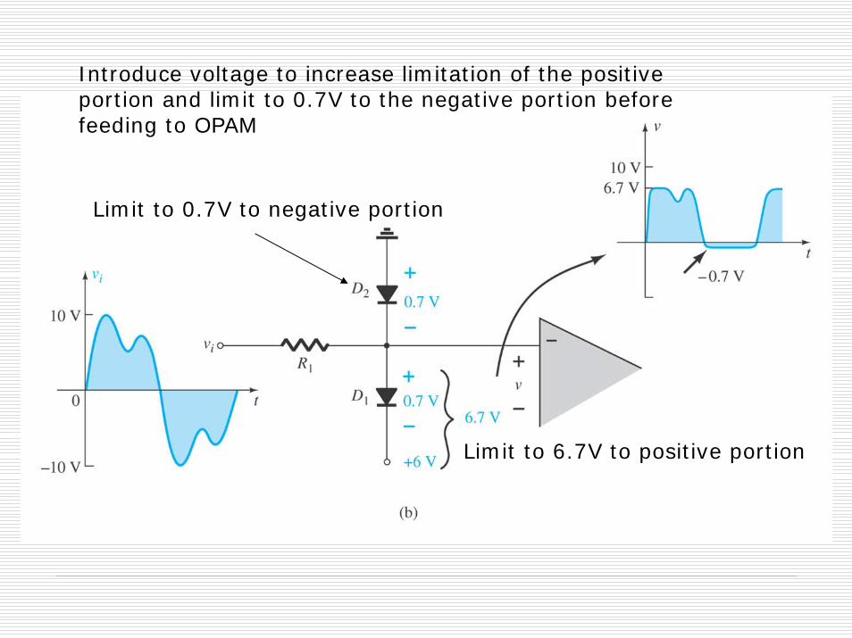
Introduce voltage to increase limitation of the positive portion and limit to 0.7V to the negative portion before feeding to OPAM
Limit to 6.7V to positive portion
Limit to 0.7V to negative portion
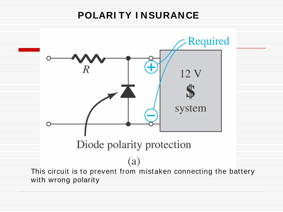
POLARITY INSURANCE
This circuit is to prevent from mistaken connecting the battery with wrong polarity
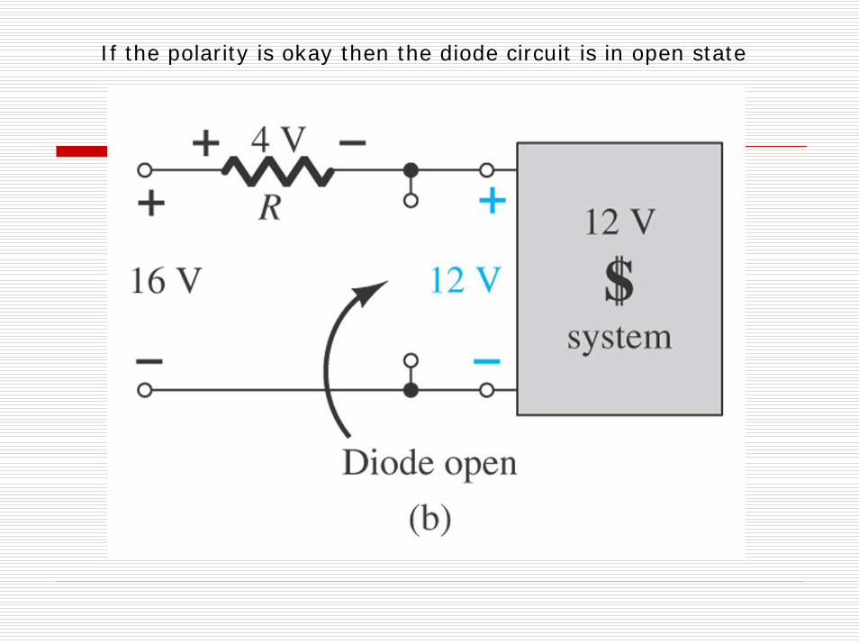
If the polarity is okay then the diode circuit is in open state

If the polarity is not okay then the current is bypass thru diode. This will stop the battery to damage the $ system

Battery –powered backup
When electrical power is connected D1 id “on” state and D2 will be “off” state, thus only electrical power is functioned. When electrical power is disconnected D1 is “off” state and D2 is conducted , thus the power will come from the battery.
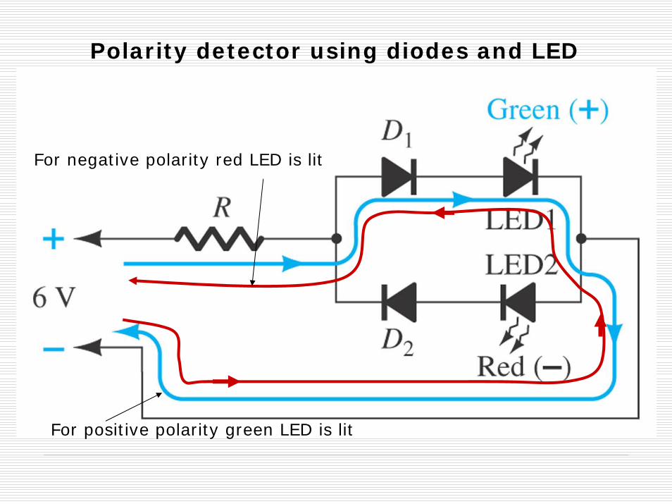
Polarity detector using diodes and LED
For positive polarity green LED is lit
For negative polarity red LED is lit

LED diodes are arranged for EXIT sign display.

Voltage Reference Levels circuit
This circuit provide different reference levels
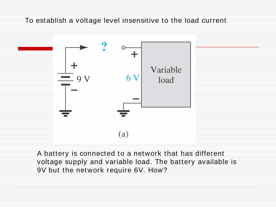
To establish a voltage level insensitive to the load current
A battery is connected to a network that has different voltage supply and variable load. The battery available is 9V but the network require 6V. How?
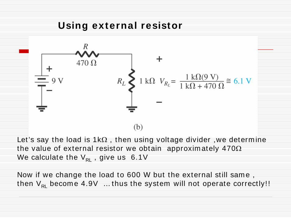
Using external resistor
Let’s say the load is 1kΩ , then using voltage divider ,we determine the value of external resistor we obtain approximately 470ΩWe calculate the VRL , give us 6.1V
Now if we change the load to 600 W but the external still same ,then VRL become 4.9V … thus the system will not operate correctly!!

Using diode
Using diode the voltage can be converted using 4 silicon diode which give a drop of voltage around 2.8V , thus the required voltage of 6.2V is obtained. This network does not sensitive to the load.

AC regulator and square-wave generator
conduct
Voltage across corresponding to the input if less than 20V
Voltage across limit to 20V

Robert L. BoylestadElectronic Devices and Circuit Theory, 9e
Copyright ©2006 by Pearson Education, Inc.Upper Saddle River, New Jersey 07458
All rights reserved.
Same configuration to produce square -wave