capacitive pcb security for active tamper and alteration
TRANSCRIPT

University of New MexicoUNM Digital Repository
Electrical and Computer Engineering ETDs Engineering ETDs
Summer 7-15-2018
Capacitive PCB Security for Active Tamper andAlteration DetectionCasey PetersenUniversity of New Mexico
Follow this and additional works at: https://digitalrepository.unm.edu/ece_etds
Part of the Electrical and Electronics Commons
This Thesis is brought to you for free and open access by the Engineering ETDs at UNM Digital Repository. It has been accepted for inclusion inElectrical and Computer Engineering ETDs by an authorized administrator of UNM Digital Repository. For more information, please [email protected].
Recommended CitationPetersen, Casey. "Capacitive PCB Security for Active Tamper and Alteration Detection." (2018). https://digitalrepository.unm.edu/ece_etds/418

i
Casey Petersen Candidate
Electrical and Computer Engineering
Department
This dissertation is approved, and it is acceptable in quality and form for publication:
Approved by the Dissertation Committee:
Jim Plusquellic , Chairperson
Payman Zarkesh-Ha
Calvin Chan

ii
CAPACITIVE PCB SECURITY FOR ACTIVE TAMPER AND
ALTERATION DETECTION
by
CASEY PETERSEN
PREVIOUS DEGREES
B.S., ENGINEERING (ELECTRICAL SYSTEMS)
M.S., ELECTRICAL ENGINEERING
THESIS
Submitted in Partial Fulfillment of the
Requirements for the degree of
Masters of Science
Electrical Engineering
The University of New Mexico
Albuquerque, New Mexico
July, 2018

iii
CAPACITIVE PCB SECURIT FOR ACTIVE TAMPER AND ALTERATION DETECTION
by
Casey Petersen
B.S., Engineering (Electrical Systems), Arizona State University 2015
ABSTRACT
The purpose of the research presented is to establish the viability of using capacitive
based sensors for the purpose of hardware security at the Printed Circuit Board (PCB) level.
Capacitive sensors are traditionally used to sense changes to the areas surrounding the sensing
pads in applications such as sensing proximity, position, humidity, fluid levels and much more.
The specific sensor used for this research is an inductor-capacitor (LC) based
Capacitance-to-Digital Converter. This configuration is virtually immune to EM noise because it
is a tank circuit and therefore filters out the noise which, in the past, caused reliability issues
with these types of sensors. The research results show that the security system is capable of
detecting active tampering as well as sensing extremely small physical alterations made to the
PCB, even if those changes occurred when the system was powered down.
In addition to establishing the viability of capacitive based PCB security, we assessed the
relationship between the sensing pad sizes and the resolution of the sensing pad. Many factors
affect the resolution of the sensing pads, the term resolution meaning how small of a change
the pads can detect reliably. These factors include the presence of power and ground planes,
floating copper, active shielding, as well as environmental factors such as variations in
temperature, humidity, and physical distance to surrounding objects.
iv
TABLE OF CONTENTS
LIST OF FIGURES ………………….………………………………………………………………………………………………. v
LIST OF TABLES ………………….……………………………………………………………………………………………….. vi
SECTOIN I. INTRODUCTION …………………….……………………………………………………………………………. 1
SECTOIN II. BACKGROUND …………………..………………………………………………………………………………. 3
SECTOIN III. METHODOLOGY ……………………………………………………………………………………………….. 4
A. Noise Mitigation ……………………..…………………………………………………………………………………… 4
B. Experimental Board Design ………………….………………………………………………………………………. 5
SECTOIN IV. RESULTS AND VERIFICATION .……..……………………………………………………………………. 7
A. Setup ……………..……………………………………………………………………………………………………………. 7
B. Results ……………….………………………………………………………………………………………………………… 8
SECTOIN V. DISCUSSION ……………………………………………………………………………………………………. 11
SECTOIN VI. CONCLUSION …………………..…………………………………………………………………………….. 13
REFERENCES ………………………………………………………………………………………………………………………. 14

v
LIST OF FIGURES
Figure 1. PCB Security Issues ……………………………………………………………………………………………………. 1
Figure 2. Pseudo Code for the D-I Algorithm ……………………………………………………………………………. 5
Figure 3. PCB Prototypes …………………….…………………………………………………………………………………… 6
Figure 4. Traces and Alterations ……………..……………………………………………………………………………….. 7
Figure 5. Capacitive Measurement Distribution …………………………………………………………………….. 12

vi
LIST OF TABLES
Table I. PCB Pad Sizes …………….………………………………………………………………………………………………... 5
Table II. Center Alteration Results ……………………………………………………………………………………………. 8
Table III. ¾ Offset Alteration Results ……………………………………………………………………………………….. 9
Table IV. Edge Alteration Results …………………………………………………………………………………………… 10

1
Section I
Introduction
There are many security threats associated with PCBs and the components which
populate them. Recent studies have shown a growing number of vulnerabilities for PCBs and the
components which populate them, both active and passive. The main categories which PCB
security issues fall into are in-field alterations, reverse engineering, and hardware Trojans [2].
These categories are broken down further in Fig. 1. In-field alterations include alterations to the
physical PCB components or traces such as rerouting or replacing components as well as
peripheral exploration. The current research on methods for detecting in-field alterations at the
PCB level is limited. The first paper addressing active protection against PCB tampering in the
field at the board level was presented in 2016 [2]. Significant efforts have been devoted to
hardware Trojans detection, security at the chip level, and security at the design and
manufacturing stages of the PCB; however, there is surprisingly limited research in the categories
of active tampering, in-field alterations, and even reverse engineering of PCBs. This paper will
address all of these areas of tamper protection.
Physical tamper detection and in-field alteration protections have previously been limited
to a single chip [11], select traces [2], and protected enclosures or envelopes [3], [6]. Paley et al.
present a trace monitoring system based on measuring the resistance of the selected lines and
comparing that value to a golden-key value previously stored for each trace monitored [2]. Any
change to the trace that altered the resistance by 0.25% or more was detectable tampering. This
system was not able to detect any tampering outside of the traces monitored and also could be

2
possibly spoofed by making alterations to the select traces while ensuring their resistance value
remained constant.
Protected enclosures and envelopes in the past have had many drawbacks. Battery
powered enclosures guarantee security as long as the sensitive data is kept only in volatile
memory. Additionally, the BBRAM must continually be supplied with power from the time it is
shipped from the factory, [3] and the battery must also be maintained through the lifetime of the
product [4]. These battery type enclosures all suffer from the same drawbacks regardless of the
enclosure type or detection method [5], [6].
Some approaches based on Physically Unclonable Functions (PUFs) are able to eliminate
the need for a battery by storing the key intrinsically in the hardware [7], [8]. PUFs rely on the
natural and manufacturing variations which are inherent in the hardware to extract a digital
fingerprint unique to the specific hardware or chip [9]. There are many uses for PUFs, even
offering limited tamper resistance when integrated into different chip designs [10].
Coated ICs [11] and optical PUFs [12] embeded in the IC offer tamper detection on power
up but do not mention real time detection. Additionally, since only the chosen IC(s) are protected,
the PCB and even IC(s) may still be vulnerable to various side channel attacks. Unless these
coatings were adopted as an industry standard, the cost of adding this to a design would be
prohibitively expensive. Even the full PCB coverage system presented in [13] and [14] fail to
address active tampering.
The goal of the research presented here is to show that nearly any physical alteration to
a PCB can be detected reliably with the addition of the proposed capacitive tamper detection
system. This is an active system capable of detecting changes that were made to the system when
it was powered down or active attempts to alter the system while in operation. The remainder
of the paper is organized as follows. Section II discusses the background on capacitive sensors
and sensor selection. Section III will cover the methodology behind the research. Section IV
reviews the results, and the design recommendations will be discussed in section V. Concluding
thoughts and possible future research is outlined in section VI.

3
Section II
Background
When selecting a sensor type for the security system, both inductive and capacitive
based proximity sensors were considered. Even though we are not sensing proximity, these
sensors are best suited to sense physical changes to their immediate surroundings. The benefits
of using an inductive sensor is that it has high accuracy for measuring changes, works in various
harsh environments, and is virtually immune to noise. The drawbacks of inductive sensors is
that they can only detect metals, are less sensitive to changes in the surrounding environment,
and they are much harder to implement on a PCB since they require coil traces rather than
pads. It is the limited material sensing and implementation difficulties that made capacitive
sensors the most appealing option for this application.
Capacitive sensors are capable of sensing any object, can sense smaller changes, and
consume less power. The drawbacks to these sensors is their sensitivity to both EM and
environmental noise such as changes in temperature and humidity, as well as their limited
accuracy for exact measurements; all of which can be easily mitigated.
Since what we desire is a binary decision on whether or not there is or has been
tampering, the lack of accuracy is not a concern. We are focused on precision and repeatably
rather than determining the exact nature or size of the alteration in question. As for the EM
noise issues, we have selected an LC based capacitve sensor which is virtually immune to EM
noise unlike capacitive sensors in the past. The environmental noise is the most difficult to deal
with.
The 28-bit FDC2214 Capacitance-to-Digital Converter from Texas Instruments is an ideal
choice for this sensing application due to the chips superior sensing resolution and noise
immunity. The chip uses an LC relaxation oscillator circuit rather than the more traditional RC
relaxation oscillator or capacitive dividers used in past capacitive sensors. Since the LC tank
circuit is used most often as a noise filter, this circuit is not afflicted by noise sources such as
florescent lights unlike the chips predecessors [16]. This EM noise immunity, along with the 28
bit resolution, makes measurements into the subfemto-farad range possible.

4
Section III
Methodology
A. Noise Mitigation
Capacitive sensors are extremely sensitive to environmental noise such as changes in
temperature, humidity, as well as the physical proximity to other objects. A temperature change
of a few degrees can yield a capacitive swing in the pico-Farad range, which is extremely
significant when we are trying to sense changes on the scale of femto-Farads. There are many
ways to filter out this noise and three of those methods are discussed here.
The first method for filtering out environmental noise is the implementation of a simple
derivative integration algorithm typically used for proximity sensing [17]. This allows us to sense
sudden changes in the environment. Pseudo code for this function can be seen in Fig. 2. If the
operation environment is expected to have little to no environmental noise, then this method
could prove to be extremely reliable. Other benefits of this method are related to the simplicity.
No memory is required to store any data and no calibration is required prior to use other than
setting your sensing times for the specific environment. The drawbacks are that you can only
sense active tampering, and if any changes are made to a system that is off, then it cannot be
detected when powered back up. The second method requires a temperature and humidity
sensor. If the swings in temperature and humidity are accurately measured, then these effects
can be filtered out and the capacitance on the sensing pad can be considered to be a constant
value. The benefits of this method are that any changes to the system can be sensed even if those
changes were made when it was powered down. The drawbacks are that the temperature or
humidity sensor could be spoofed and active tampering may be possible. Multiple temperature
and humidity sensors could be used to increase the difficulty of spoofing without being detected.
The Third and recommended method for filtering out environmental noise requires using
multiple sensing pads. This allows for the pads to be compared against one another. The relative
capacitance of each pad when compared against each other will tell you if something has been

5
sensed or not. This could be either multiple pads compared against one another or all of the pads
compared against a single calibration pad. Even if these pads are not the same shape and size,
their relative capacitance will still drift up or down along a predictable curve in relation to one
another. The benefits of this method are that any changes to the system can be sensed even if
those changes were made when it was powered down. Additionally, the sensors cannot be easily
spoofed and the reliability of the system goes up as more pads are used. The drawback of this
method is that a calibration of the system is required and there must be storage space for that
calibration data. There are many other well-known methods that could be used for filtering out
noise and most of them will require the use of multiple sensing pads. Other methods could
reduce the amount of data that is required to be stored and even automate the
calibration/learning process but these methods will not be discussed further here.
B. Experimental Board Design
Four different experimental boards were designed based on a 4x6 inch board size. Copper
tape was placed over a 4x6 inch area of fiberglass and then the tape was divided into equal
sections of 2, 4, 8 and 16 to be used as the sensing pads. Table I gives breakdown of each board
and the corresponding sensing pad size and area.

6
Holes were drilled through the center of each sensing pad and header pins were soldered
on through the back of the PCBs. The finished test PCBs in Fig. 3 give a back view of the pads,
header pins and substrates. The thickness of materials used is as follows, fiberglass substrate: 25
mills, Copper Tape: 3 mills, Paper: 3 mills. The paper was glued directly to the sensing pads and
used as a dielectric to separate the traces from the sensing pads (reference Fig. 4). This thickness
of paper was specifically chosen because this is the minimum separation a designer can expect
to achieve from most PCB fabrication shops. Traces were placed in three different locations on
each PCB directly over the center of a pad, between two pads, and offset by 3/4 of a pad. This
allowed data to be collected for the location of alterations made.
7
Section IV
Results and Verification
A. Setup
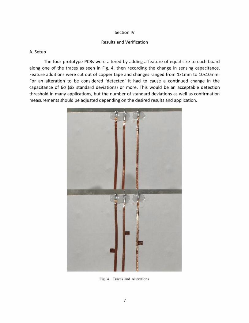
The four prototype PCBs were altered by adding a feature of equal size to each board
along one of the traces as seen in Fig. 4, then recording the change in sensing capacitance.
Feature additions were cut out of copper tape and changes ranged from 1x1mm to 10x10mm.
Fo a alte atio to e o side ed ’dete ted’ it had to ause a o ti ued ha ge i the apa ita e of σ (si sta da d de iations) or more. This would be an acceptable detection
threshold in many applications, but the number of standard deviations as well as confirmation
measurements should be adjusted depending on the desired results and application.

8
In order to obtain the maximum standard deviation for each pad, 100 readings were
obtained over a one-minute period for calibration and then again after an alteration. If a larger
standard deviation was recorded at any point, then the maximum standard deviation for that pad
size was updated. An additional calibration pad was recorded throughout the sensing process to
ensure that the maximum standard deviation was not exceeded during each test.
B. Results
The results from the experiments can be seen in Tab. II, Tab. III and Tab. IV. The tolerances
to these alterations are within 0.5 mm each, thus there is some measurement variation which is
due to lack of precision. Table II reflects the best-case scenario for sensing changes made to a
board; Altering the board in the center of one of the sensing pads is where maximum capacitive
coupling takes place and where the greatest change in capacitance will be seen. The values for
each test in Table II are generally larger than the two other areas tested on the sensing pad.
Keeping with our σ se si g o e tio , the -pad configuration is seen to have the least amount
of resolution. This is more due to the larger standard deviation than the actual change in
capacitance experienced. In fact, the largest pads on board A experienced a 53.7 femtoFarad (fF)
change in capacitance for a 1x1mm alteration while the smallest pads on board D only
experienced a change of 22.7 fF for the same alteration.
Due to the much larger standard deviation, the change in board A caused by the 1x1mm
alteration was o l . σ a a f o the ea hile the sa e alte atio i oa d D aused a

9
ha ge of . σ. The sta da d de iatio of a oa d a e lo e ed th ough the use of a ti e o ground shielding in addition to other methods discussed in section V. With the given threshold
set for sensing alterations, board A was capable of sensing changes made over the center of the
sensing pads of 5x5mm or larger; Board B was able to sense changes of approximately 2x2 mm
or larger, and board C as well as board D were easily able to sense the smallest change of 1x1mm.
It is important to note that the changes made in the experiments chosen are virtually two
dimensional. Since the capacitive coupling effect relies on both the distance to an object as well
as the surface area of that object, the addition or removal of a three-dimensional object with a
similar footprint would cause a greater change in capacitance and therefore be easier to sense.
Table III summarizes the experimental results from an alteration made not directly over
the center of a pad, but rater offset by 3/4 of the sensing pad. The results are virtually the same
as those found in Tab. II with only a slight reduction in the sensing resolution. A few of the
measurements that are slightly above those found in the previous experiments are likely due to
a lack of precision and repeatability in the alterations made between the two experiments.
Alterations made to the edge of a pad were the hardest to sense. Table IV shows a
reduction in sensing capability by about half when compared with the results from the original
experiment. board A was just able to sense a change of 10x10mm, even though the area
overlapping the pad was nearly double that of the 5x5mm pad sensed in Tab. II. Board B would
be capable of sensing changes just larger than 2x2mm while boards C and D were still able to
easily sense the smallest of changes.

10
These results were not obtained on an optimal board design or with optimal
environmental conditions. An environmental chamber could improve the results received, but
they would also be unrealistic for real world applications. With proper PCB design constraints,
better results could be obtained, even in the presence of more environmental noise.

11
Section V
Discussion
Many factors affect the measurement resolution. These factors include sensing pad sizes,
the presence of power and ground planes, floating copper, active shielding, tolerable number of
false alarms, as well as the amount of environmental noise present. While the boards design is
mostly under the control of the design engineer, the environmental factors may greatly lower
the capabilities of the system and be the most difficult to control. The implementation of a
shielded container can greatly reduce or even eliminate the effects of environmental noise.
An optimal design for this system, in terms of measurement resolution, would use
numerous small sensing pads backed by active shielded planes. These active shielded planes and
even the sensing planes could be used as a Faraday cage ground, addition coupling, or other
application when not being actively used for sensing board changes. The active shielding works
by taking the same signals sent to the sensing pads and puts it through a unity buffer. Active
shielding greatly increases the measurement resolution and is frequently used in proximity
sensing applications in order to increase the sensing distance.
The sensing pads can either be placed in the dead space on the top and bottom layers of
the PCB or on the layers directly below the outer most layers. The sensing pads can be any shape
and size but as the size increases the standard deviation of measurements increases as well,
resulting in lower resolution. If sensing layers are set into the PCB then the manufacturing notes
should request that the first and last dielectric layers of the design be 2-3 mills thick, which is the
current industry recommended minimum for most PCB fabrication shops. The materials used in
the design are not important in terms of the capacitance readings or measurement resolution.
Different materials and thicknesses will just have a different initial capacitive offset.
Removing power and ground planes in a PCB design is rarely recommended, although this
may be the second-best choice if active shielding is not possible. The presence of the power and
ground planes will reduce the sensitivity of the sensing pads but also reduce the noise. As
previously discussed, a reduction in environmental noise means a reduction in the standard
deviation. Depending on the operation environment, the addition of passive shielding may even
increase the sensing resolution of the system. Additionally, increasing the separation distance
between power/ground planes and the sensing pads is recommended. The closer the sensing
pad is to a power/ground plane, the lower the measurement resolution will be [18].
To determine what constitutes a positive tamper detection, the system must be
calibrated to the operation environment and the number of acceptable false alarms in a given
time period must be set. A simple function can be used to determine the maximum standard
deviation of the system for a given operating environment. The number of floating average
samples, standard deviation samples and calibration run time will depend on the operating
environment.

12
A lab with good climate control may only require a calibration of a few minutes, while
some outdoor and other environments may require 24 hours or multiple calibrations. After the
maximum standard deviation is set and the maximum percent of acceptable false alarms is
determined, then the detection zone can be set. The detection zone is determined by how many
standard deviations away from the mean you need to be. The distribution is Gaussian as shown
i Fig. , thus the likelihood that a gi e easu e e t is ithi σ of the p edi ted ea is app o i atel %, σ = %, σ = %, σ = %, a d σ = %. Si e the maximum standard
deviation was used, these percentages will be higher the majority of the time. Multiple
confirming measurements will also greatly reduce or eliminate false alarms.

13
Section IV
Conclusion
We have presented a novel approach for detecting active tampering and in-field
alterations to a PCB. We have shown that this system is capable of detecting alterations made to
traces on a PCB with an area less than 1 mm. The system requires relatively little overhead in
terms of hardware and memory and consumes very little power. The proposed system is capable
of detecting nearly every physical in-field alteration as well as inhibit efforts to clone or reverse
engineer a PCB.
There is still a significant amount of research that needs to be carried out on this system
and questions that need be answered. Future research should focus on implementing the system
on existing PCB designs and testing precise and repeatable alterations to the boards. A proper
implementation of the system must ensure that the hardware cannot be bypassed or spoofed.
Specifics on system design and the effects of different operating environments must be tested to
optimize the sensing resolution for each application. The frequency of the sensing circuit and the
passive components used with the FDC2214 chip can also have a great impact on the results.

14
References
[1] Z. Guo J. Di M. Teh a ipoo D. Fo te ”I estigatio of O fus atio ased Anti-Reverse
E gi ee i g fo P i ted Ci uit Boa ds” Desig Auto atio Co fe e e . [2] S. Pale T. Ho ue S. Bhu ia ”A ti e p ote tio agai st p ph si al ta pe i g” Qualit Ele t o i
Design (IS QED) 2016 17th International Symposium on pp. 356-361 2016.
[3] P. Isaacs, T. Morris Jr, M. J. Fisher, and K. Cuthbert, Tamper Proof,Tamper Evident Encryption
Technology, in Pan Pacific Symposium. SMTA, 2013.
[4] IBM, IBM 4765 Cryptographic Coprocessor Security Module, 2012. [5] H. Eren and L. Sandor,
Fringe-Effect Capacitive Proximity Sensors for Tamper Proof Enclosures, in Sensors for Industry
Conference, 2005.
[5] H. Eren and L. Sandor, Fringe-Effect Capacitive Proximity Sensors for Tamper Proof Enclosures, in
Sensors for Industry Conference, 2005.
[6] R. Burke and C. Queen, A security housing for a circuit, 2004, WO Patent App.
PCT/IE2004/000,043.
[7] B. Gassend, D. Clarke, M. v. Dijk, and S. Devadas, Silicon Physical Random Functions, in ACM CCS,
2002.
[8] C. Herder, M. Yu, F. Koushanfar, and S. Devadas, Physical Unclonable Functions and Applications,
Proceedings of the IEEE, vol. 102, 2014.
[9] J. Delvaux, D. Gu, D. Schellekens, and I. Verbauwhede, Helper data algorithms for PUF-based key
generation: Overview and analysis, IEEE Transactions on Computer-Aided Design of Integrated
Circuits and Systems, vol. 34, no. 6, pp. 889902, 2015.
[10] C. Helfmeier, D. Nedospasov, C. Tarnovsky, J. S. Krissler, C. Boit, and J.-P. Seifert, Breaking and
entering through the silicon, in ACM Conference on Computer and Communications Security
(CCS), 2013.
[11] P. Tuyls, G.-J. Schrijen, B. Skoric, J. van Geloven, N. Verhaegh, and R. Wolters, Read-Proof
Hardware from Protective Coatings, in CHES, ser. LNCS, 2006, vol. 4249.
[12] T. Esbach, W. Fumy, O. Kulikovska, D. Merli, D. Schuster, and F. Stumpf, A New Security
Architecture for Smartcards Utilizing PUFs, in ISSE Conference, 2012.
[13] M. Spain, B. Fuller, K. Ingols, and R. Cunningham, Robust keys from physical unclonable
functions, in IEEE International Symposium on Hardware-Oriented Security and Trust (HOST),
2014, pp. 8892.
[14] M. Vai, B. Nahill, J. Kramer, M. Geis, D. Utin, D. Whelihan, and R. Khazan, Secure architecture for
embedded systems, in IEEE High Performance Extreme Computing Conference (HPEC), 2015.
[15] S. Ghosh, A. Basak, and S. Bhunia, How Secure are Printed Circuit Boards against Trojan
Attacks?, IEEE Design Test, 2014.
[16] FDC2x1x EMI-Resistant 28-Bit,12-Bit Capacitance-to-Digital Converter for Proximity and Level
Sensing Applications. Texas Instruments, Dallas, Jun-2015.
[17] Y. Yu, Capacitive Proximity Sensing Using FDC2x1y. Texas Instruments, Oct-2015.
[18] D. Wang, Derivative Integration Algorithm for Proximity Sensing. Texas Instruments, Dallas, Sep-
2015.