capability assessment of inkjet printing for reliable...
TRANSCRIPT

TDMR-2016-11-0259-R
Copyright © 2016 IEEE. Personal use of this material is permitted. However, permission to use this material for any other
purposes must be obtained by sending a request to [email protected]
1
Abstract— In this paper, inkjet-printed silver traces and
interconnections produced with the print-on-slope technique were
used in an RFID structure operating in the UHF range. Underfill
material was used to attach silicon RFID chips onto flexible, 125-
µm-thick polymer substrates. The cured underfill was also used
as a sloped surface for printing interconnection traces from the
chip to the plastic substrate's radiators. Inkjet printing was
performed in one phase, producing both the interconnections to
the chip and the radiators. This enables the use of a single-phase
continuous roll-to-roll compatible process instead of the
commonly used two-phase stop-and-go process. To further
investigate the behavior of printed low-temperature nanoparticle
ink and its compatibility with different substrate materials, basic
conductive traces were printed onto the substrates.
Thereafter, the structures were exposed to thermal/humidity
tests at 85 °C temperature/85% relative humidity ("85/85") for
up to a 2000-hour period. To gain an understanding of the
response of the structures under stressing, the samples were
intermittently characterized using a read range measurement
device, followed by removal of failed samples from the test. The
samples were characterized also by optical imaging and field-
emission scanning electron microscopy (FE-SEM). The bulk
conductive traces were characterized electrically by measuring
their resistances during test breaks.
The results point out that, although some challenges are still to
be overcome, inkjet printing is a feasible way of producing
conductive traces for RFID structures, and that the print-on-slope
technique is utilizable also in practical applications as a cost-
effective method with adequate reliability for producing
interconnections between chip and substrate.
Index Terms—85/85 test, Direct chip attachment, Inkjet,
Interconnections, Reliability
Manuscript received June 27, 2016. This work was supported by
Meadville Aspocomp, Nokia, Premix, UPM-Raflatac, and the Finnish
Funding Agency for Innovation (Tekes). J. Putaala acknowledges the support
in the form of grants from the Finnish Foundation for Technology Promotion
(TES), the Riitta and Jorma J. Takanen foundation, and The Nokia
Foundation. M. Mäntysalo is supported by Academy of Finland grant No.
288945 and 294119.
J. Putaala, J. Hannu, S. Myllymäki, Juha Hagberg, and Heli Jantunen are
with the Microelectronics Research Unit, University of Oulu, P.O. Box 4500,
FI 90014 Oulu, Finland. Phone: +358-294-487-962; fax: +358-8-553-2728;
e-mail: [email protected] (J. Putaala).
J. Niittynen is with the Meyer Burger B.V., Luchthavenweg 10 5657 EB
Eindhoven, The Netherlands.
E. Kunnari is with the Tampere University of Applied Sciences, Kuntokatu
3, FI 33520 Tampere, Finland.
M. Mäntysalo is with the Department of Electronics and Communications
Engineering, Tampere University of Technology, P.O. Box 692, FI 33101
Tampere, Finland
I. INTRODUCTION
NKJET-printed electronics (IPE) is one potential additive
manufacturing solution in current and future low-cost
electronics due to its material efficiency, ease of production
and customization, low cost of processing equipment, and
environmental aspects [1-3]. Some other considerable additive
manufacturing technologies are material extrusion, powder bed
fusion, binder jetting, vat photo-polymerization, directed
energy deposition, and sheet lamination [4].
The rather low processing temperatures of advanced silver
inks of around 150 °C enable the use of a wider scale of
materials and structural solutions than, for example, with
traditional printed circuit board technology with surface mount
devices [5, 6]. The minimum width of inkjet-printed lines is
defined by the drop volume, which in commonly used modern
technology can be around 1 pl. This results in a drop diameter
of about 25 µm on the substrate, depending on the ink, the
surface, and the use of surface modifiers [7]. State-of-the-art
technology (Electrohydrodynamic EHD printing) suggests that
a scale of 0.1 femtoliter is available, which is capable of
producing line widths on a micrometer scale [8]. In addition to
the aforementioned factors, the electrical conductivities of
silver inks enable their use in a wide variety of applications
reaching up to the GHz range [9-11].
In this research, inkjet printing was used to fabricate an
RFID tag's radiator traces on planar substrates, simultaneously
with interconnections, with the so-called print-on-slope
technique, for RFID chips. The operating band of the chips
was in the ultra-high-frequency (UHF) range, at 865-868 MHz.
While inkjet-printing of RFID antennas has been demonstrated
earlier by various research groups, fabrication of the entire tag
structure including the component interconnection is a new
technique [12, 13]. This was complemented by another test set
with planar conducting traces for observing the effect of
stressing in the cured ink.
To characterize reliability, the fabricated test structures
were put into a thermal/humidity test chamber ("85/85" test)
and their read ranges were measured intermittently during test
breaks. Finally, SEM imaging was used to characterize the
samples, including crack locations in the structures and
qualitative analysis of the prints. The basic inkjet-printed lines
were measured and visually inspected during test breaks to
Capability Assessment of Inkjet Printing for
Reliable RFID Applications
Jussi Putaala, Juha Niittynen, Jari Hannu, Sami Myllymäki, Esa Kunnari, Matti Mäntysalo, Member,
IEEE, Juha Hagberg, Heli Jantunen, Member, IEEE
I
TDMR-2016-11-0259-R
Copyright © 2016 IEEE. Personal use of this material is permitted. However, permission to use this material for any other
purposes must be obtained by sending a request to [email protected]
2
observe how the resistances and adhesion of silver ink on
different substrates are affected by an elevated
thermal/humidity environment.
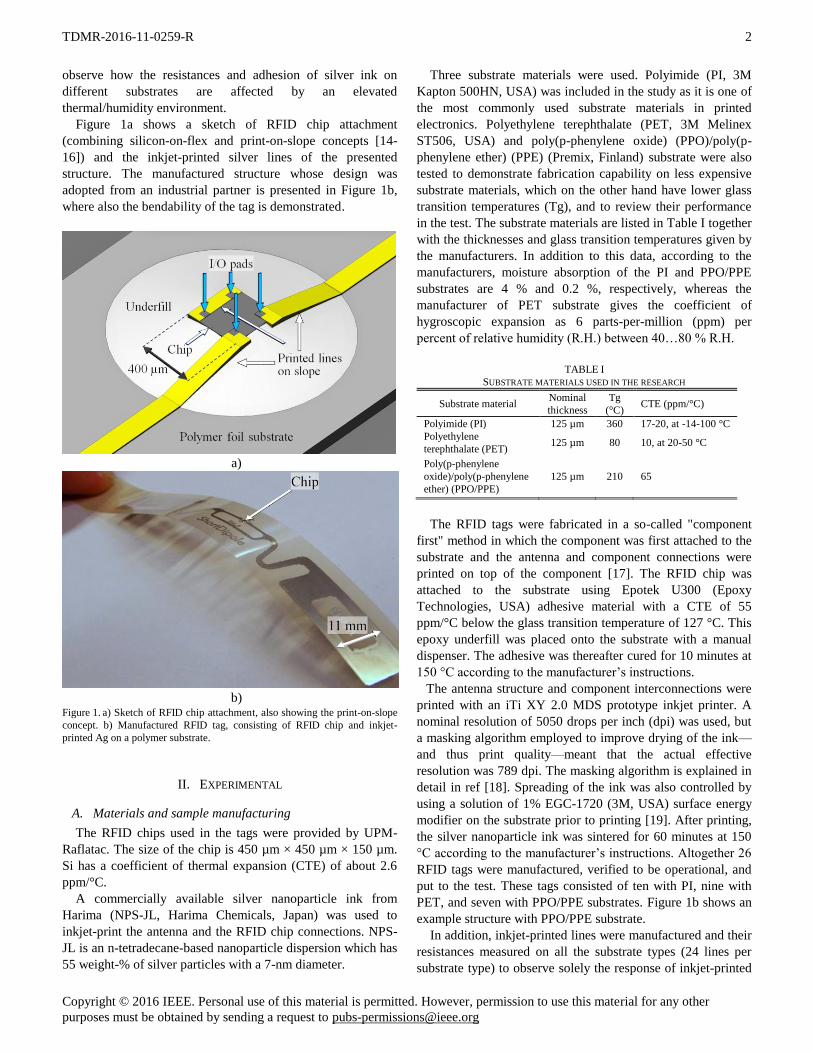
Figure 1a shows a sketch of RFID chip attachment
(combining silicon-on-flex and print-on-slope concepts [14-
16]) and the inkjet-printed silver lines of the presented
structure. The manufactured structure whose design was
adopted from an industrial partner is presented in Figure 1b,
where also the bendability of the tag is demonstrated.
a)
b)
Figure 1. a) Sketch of RFID chip attachment, also showing the print-on-slope
concept. b) Manufactured RFID tag, consisting of RFID chip and inkjet-
printed Ag on a polymer substrate.
II. EXPERIMENTAL
A. Materials and sample manufacturing
The RFID chips used in the tags were provided by UPM-
Raflatac. The size of the chip is 450 µm × 450 µm × 150 µm.
Si has a coefficient of thermal expansion (CTE) of about 2.6
ppm/°C.
A commercially available silver nanoparticle ink from
Harima (NPS-JL, Harima Chemicals, Japan) was used to
inkjet-print the antenna and the RFID chip connections. NPS-
JL is an n-tetradecane-based nanoparticle dispersion which has
55 weight-% of silver particles with a 7-nm diameter.
Three substrate materials were used. Polyimide (PI, 3M
Kapton 500HN, USA) was included in the study as it is one of
the most commonly used substrate materials in printed
electronics. Polyethylene terephthalate (PET, 3M Melinex
ST506, USA) and poly(p-phenylene oxide) (PPO)/poly(p-
phenylene ether) (PPE) (Premix, Finland) substrate were also
tested to demonstrate fabrication capability on less expensive
substrate materials, which on the other hand have lower glass
transition temperatures (Tg), and to review their performance
in the test. The substrate materials are listed in Table I together
with the thicknesses and glass transition temperatures given by
the manufacturers. In addition to this data, according to the
manufacturers, moisture absorption of the PI and PPO/PPE
substrates are 4 % and 0.2 %, respectively, whereas the
manufacturer of PET substrate gives the coefficient of
hygroscopic expansion as 6 parts-per-million (ppm) per
percent of relative humidity (R.H.) between 40…80 % R.H.
TABLE I
SUBSTRATE MATERIALS USED IN THE RESEARCH
Substrate material Nominal
thickness
Tg
(°C) CTE (ppm/°C)
Polyimide (PI) 125 µm 360 17-20, at -14-100 °C
Polyethylene
terephthalate (PET) 125 µm 80 10, at 20-50 °C
Poly(p-phenylene
oxide)/poly(p-phenylene
ether) (PPO/PPE)
125 µm 210 65
The RFID tags were fabricated in a so-called "component
first" method in which the component was first attached to the
substrate and the antenna and component connections were
printed on top of the component [17]. The RFID chip was
attached to the substrate using Epotek U300 (Epoxy
Technologies, USA) adhesive material with a CTE of 55
ppm/°C below the glass transition temperature of 127 °C. This
epoxy underfill was placed onto the substrate with a manual
dispenser. The adhesive was thereafter cured for 10 minutes at
150 °C according to the manufacturer’s instructions.
The antenna structure and component interconnections were
printed with an iTi XY 2.0 MDS prototype inkjet printer. A
nominal resolution of 5050 drops per inch (dpi) was used, but
a masking algorithm employed to improve drying of the ink—
and thus print quality—meant that the actual effective
resolution was 789 dpi. The masking algorithm is explained in
detail in ref [18]. Spreading of the ink was also controlled by
using a solution of 1% EGC-1720 (3M, USA) surface energy
modifier on the substrate prior to printing [19]. After printing,
the silver nanoparticle ink was sintered for 60 minutes at 150
°C according to the manufacturer’s instructions. Altogether 26
RFID tags were manufactured, verified to be operational, and
put to the test. These tags consisted of ten with PI, nine with
PET, and seven with PPO/PPE substrates. Figure 1b shows an
example structure with PPO/PPE substrate.
In addition, inkjet-printed lines were manufactured and their
resistances measured on all the substrate types (24 lines per
substrate type) to observe solely the response of inkjet-printed

TDMR-2016-11-0259-R
Copyright © 2016 IEEE. Personal use of this material is permitted. However, permission to use this material for any other
purposes must be obtained by sending a request to [email protected]
3
lines to stressing. Examples of Ag lines on PI, PET, and
PPO/PPE substrates are shown (after stress test) in Figure 2a-
c, respectively. Some extraneous spreading of ink on each of
the substrates can also be observed.
a)
b)
c)
Figure 2. Laser microscopy images of the design used in simple resistance
monitoring of cured ink during the test breaks. Images taken after stress test
from prints on a) PI, b) PET, c) PPO/PPE substrates.
B. Stress tests
Moisture absorption of polymer materials can be a challenge
to reliable operation of electronics. Therefore, to characterize
the reliability of the RFID tags, an "85/85"
temperature/humidity (T/H) life test was used [20]. The
standard defines the temperature as 85 ± 2 °C and relative
humidity as 85 ± 5 %. The test time is defined as at least 1000
hours. The 85/85 accelerated stress test was chosen to study
whether or not—besides elevated temperature—the moisture
absorption of polymer affects the reliable operation of printed
RFID devices.
The total stress time for the printed RFID tags was 1724
hours and the tags were taken out for inspection nine times.
The stress time between inspections varied from 139 to 353
hours, while the median stress interval was about 160 hours.
The bulk conductors were measured during the same intervals;
however, their stressing was continued up to 2007 hours.
C. Characterization methods
Before the tests and during the stress intervals the RFID tags
were inspected visually and their functionality verified.
Functional verification, presented in detail in ref. [21], was
done using a Voyantic Tagformance lite RFID test chamber
(Voyantic, Finland) to make sure each of the RFID tags
responded to the RFID transponder. Changes in read ranges
were characterized during the stress test intervals by
contrasting those measurements to the initially measured read
ranges. No specific read range threshold for determining a tag
as failed was used, but it was deemed failed when it did not
respond to the transponder at all.
Resistances of basic conductive lines were measured during
the test breaks to observe the response of the cured ink to
stressing.
Imaging of the samples was done with an optical
microscope and a (field emission) scanning electron
microscope (FE-SEM). In addition, laser microscopy was used
to support these imaging methods. Optical microscope images
were taken from the top of the samples to observe the inkjet-
printed interconnections and traces. SEM images were taken
from a slight angle near the top of the samples to observe
especially the interconnection area of the conductor traces near
the RFID chips. Selected samples were immersed in an epoxy
resin and dried, followed by careful grinding and polishing to
reveal the cross-sections of the RFID structures.
III. RESULTS
A. Read range measurements of RFID structures
Before stress testing, the measured read ranges averaged 5.8
m, with a range of 4.4-7.0 meters. The data related to the read
range measurements of the structures on each substrate are
presented in Table II.
TABLE II
TEST SET DATA
Property
Substrate material
PI PET PPO/PPE
Number of samples 10 9 7
Broken after test (1724 hrs.) 7 6 1
Average read range (m) 6.21 5.45 5.70
-Standard deviation (m) 0.66 0.42 0.81
Average change in read range (m) 0.11 0.32 0.35
Amount of samples with increased
read range in the end compared to start 1 7 4
Examples of read range measurement results of RFID
tags obtained during intervals of the test is presented in Figure
3a-c. No remarkable degradation in the read ranges has
occurred in these case after 1724 hours of testing. In Figure 3b
and c, the maximum read range has actually increased at the
end compared to the start of the tests, being as much as 1.291
m for the PPO case, Figure 3c. This behavior was observed
with 7 out of 9 and 4 out of 7 of the samples printed onto PET
and PPO/PPE substrates, respectively. With PI substrates the
last read range measurements, taken either before breakdown
of the sample or at the end of the test, were lower than the
initial values in all except one PI sample (also, one PI sample
was broken during the first stress test interval, between 0-164
hours). For the failed tags the change from functioning to
failed was sudden, i.e. it occurred within one testing interval,
and no indications of failures were observed beforehand.

TDMR-2016-11-0259-R
Copyright © 2016 IEEE. Personal use of this material is permitted. However, permission to use this material for any other
purposes must be obtained by sending a request to [email protected]
4
a)
b)
c)
Figure 3. Read range measurement results of RFID tags at different phases of
the test, showing the peak read range in the operating band. a) PI, b) PET, c)
PPO/PPE.
On the basis of the read range measurements, Figure 4
shows the percentual amount of failed RFID tags as a function
of time periods of stress testing where the tag has failed. The
figure suggests that the tags using PPO/PPE as a substrate
material had better reliability with no failures after 1000 hours
of testing, and one failed tag out of seven after the test, thus
indicating that 14 % of the population failed, while tags with
PI and PET as a substrate were somewhat less reliable.
Figure 4. Amount of failed RFID tags as a function of test time.
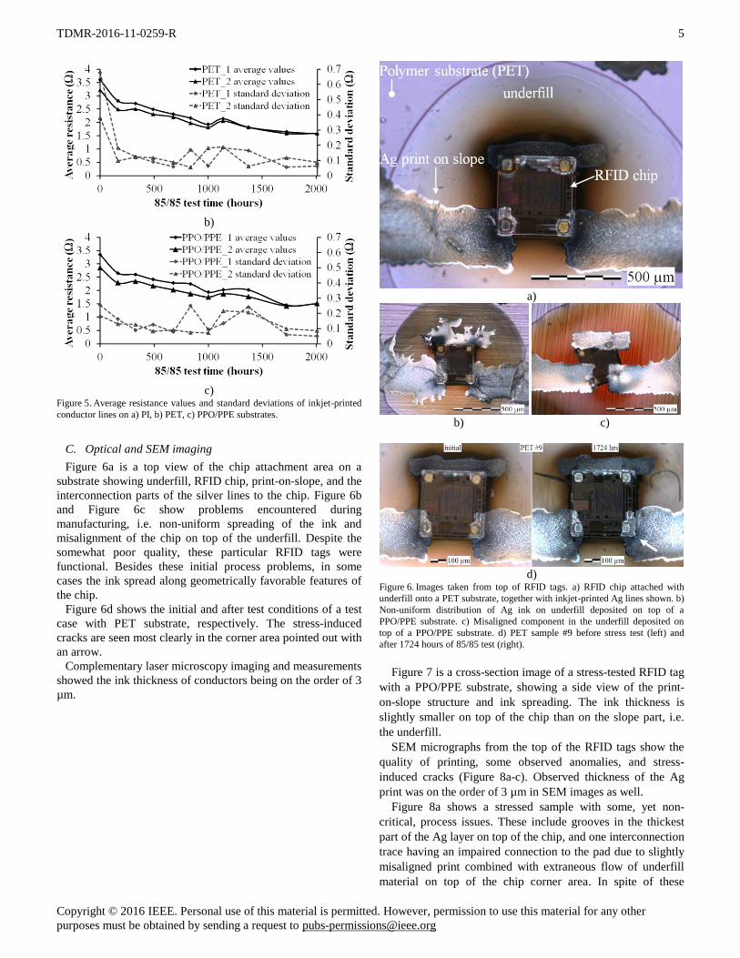
B. Resistance measurements of inkjet-printed conductor
lines
Resistance measurements of the printed lines were done on
each of the three substrate types. Two individual samples of
each substrate type were used, with 12 lines printed on both,
i.e. 24 lines per substrate type were measured. The averaged
resistances and standard deviations of the lines on each
substrate are presented in Figure 5. For lines printed on PET
and PPO/PPE substrates, clearly decreasing trends in the
averaged resistance values can be seen, whereas for the PI
substrate, this trend does not exist. The average standard
deviations of the resistances in the whole testing period were
1.1 and 0.42 for substrates PI_1 and PI_2, respectively; 0.17
and 0.14 for PET_1 and PET_2, respectively; and 0.14 and
0.12 for PPO/PPE_1 and PPO/PPE_2, respectively. The
adhesion of the printed conductors to the PI substrates was
found to be poor.
During the testing a total of six printed resistance
measurement lines failed during four intervals, all on PI
substrates, see Figure 5a. In the figure, points i)–iv) show
failures that occurred between i) 490-678 hours, ii) 678-837
hours, iii) 1000-1139 hours, and iv) 1724-2007 hours,
respectively.
a)
TDMR-2016-11-0259-R
Copyright © 2016 IEEE. Personal use of this material is permitted. However, permission to use this material for any other
purposes must be obtained by sending a request to [email protected]
5
b)
c)
Figure 5. Average resistance values and standard deviations of inkjet-printed
conductor lines on a) PI, b) PET, c) PPO/PPE substrates.
C. Optical and SEM imaging
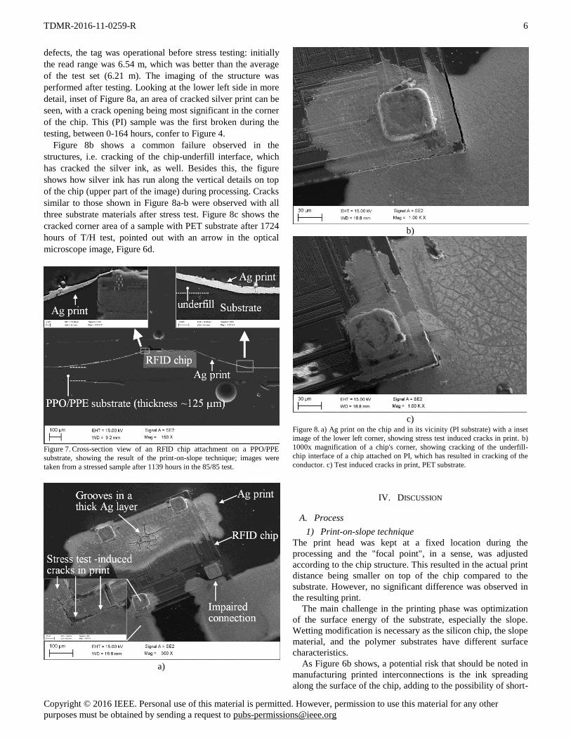
Figure 6a is a top view of the chip attachment area on a
substrate showing underfill, RFID chip, print-on-slope, and the
interconnection parts of the silver lines to the chip. Figure 6b
and Figure 6c show problems encountered during
manufacturing, i.e. non-uniform spreading of the ink and
misalignment of the chip on top of the underfill. Despite the
somewhat poor quality, these particular RFID tags were
functional. Besides these initial process problems, in some
cases the ink spread along geometrically favorable features of
the chip.
Figure 6d shows the initial and after test conditions of a test
case with PET substrate, respectively. The stress-induced
cracks are seen most clearly in the corner area pointed out with
an arrow.
Complementary laser microscopy imaging and measurements
showed the ink thickness of conductors being on the order of 3
µm.
a)
b) c)
d)
Figure 6. Images taken from top of RFID tags. a) RFID chip attached with
underfill onto a PET substrate, together with inkjet-printed Ag lines shown. b)
Non-uniform distribution of Ag ink on underfill deposited on top of a
PPO/PPE substrate. c) Misaligned component in the underfill deposited on
top of a PPO/PPE substrate. d) PET sample #9 before stress test (left) and
after 1724 hours of 85/85 test (right).
Figure 7 is a cross-section image of a stress-tested RFID tag
with a PPO/PPE substrate, showing a side view of the print-
on-slope structure and ink spreading. The ink thickness is
slightly smaller on top of the chip than on the slope part, i.e.
the underfill.
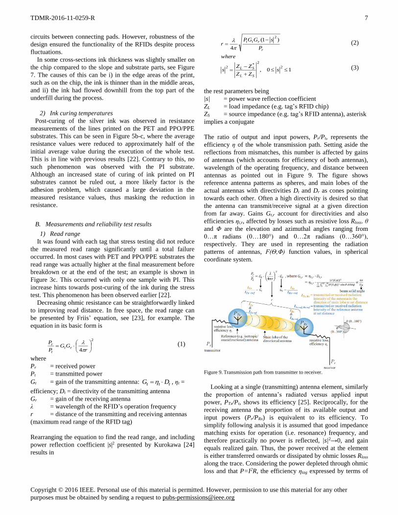
SEM micrographs from the top of the RFID tags show the
quality of printing, some observed anomalies, and stress-
induced cracks (Figure 8a-c). Observed thickness of the Ag
print was on the order of 3 µm in SEM images as well.
Figure 8a shows a stressed sample with some, yet non-
critical, process issues. These include grooves in the thickest
part of the Ag layer on top of the chip, and one interconnection
trace having an impaired connection to the pad due to slightly
misaligned print combined with extraneous flow of underfill
material on top of the chip corner area. In spite of these
TDMR-2016-11-0259-R
Copyright © 2016 IEEE. Personal use of this material is permitted. However, permission to use this material for any other
purposes must be obtained by sending a request to [email protected]
6
defects, the tag was operational before stress testing: initially
the read range was 6.54 m, which was better than the average
of the test set (6.21 m). The imaging of the structure was
performed after testing. Looking at the lower left side in more
detail, inset of Figure 8a, an area of cracked silver print can be
seen, with a crack opening being most significant in the corner
of the chip. This (PI) sample was the first broken during the
testing, between 0-164 hours, confer to Figure 4.
Figure 8b shows a common failure observed in the
structures, i.e. cracking of the chip-underfill interface, which
has cracked the silver ink, as well. Besides this, the figure
shows how silver ink has run along the vertical details on top
of the chip (upper part of the image) during processing. Cracks
similar to those shown in Figure 8a-b were observed with all
three substrate materials after stress test. Figure 8c shows the
cracked corner area of a sample with PET substrate after 1724
hours of T/H test, pointed out with an arrow in the optical
microscope image, Figure 6d.
Figure 7. Cross-section view of an RFID chip attachment on a PPO/PPE
substrate, showing the result of the print-on-slope technique; images were
taken from a stressed sample after 1139 hours in the 85/85 test.
a)
b)
c)
Figure 8. a) Ag print on the chip and in its vicinity (PI substrate) with a inset
image of the lower left corner, showing stress test induced cracks in print. b)
1000x magnification of a chip's corner, showing cracking of the underfill-
chip interface of a chip attached on PI, which has resulted in cracking of the
conductor. c) Test induced cracks in print, PET substrate.
IV. DISCUSSION
A. Process
1) Print-on-slope technique
The print head was kept at a fixed location during the
processing and the "focal point", in a sense, was adjusted
according to the chip structure. This resulted in the actual print
distance being smaller on top of the chip compared to the
substrate. However, no significant difference was observed in
the resulting print.
The main challenge in the printing phase was optimization
of the surface energy of the substrate, especially the slope.
Wetting modification is necessary as the silicon chip, the slope
material, and the polymer substrates have different surface
characteristics.
As Figure 6b shows, a potential risk that should be noted in
manufacturing printed interconnections is the ink spreading
along the surface of the chip, adding to the possibility of short-
TDMR-2016-11-0259-R
Copyright © 2016 IEEE. Personal use of this material is permitted. However, permission to use this material for any other
purposes must be obtained by sending a request to [email protected]
7
circuits between connecting pads. However, robustness of the
design ensured the functionality of the RFIDs despite process
fluctuations.
In some cross-sections ink thickness was slightly smaller on
the chip compared to the slope and substrate parts, see Figure
7. The causes of this can be i) in the edge areas of the print,
such as on the chip, the ink is thinner than in the middle areas,
and ii) the ink had flowed downhill from the top part of the
underfill during the process.
2) Ink curing temperatures
Post-curing of the silver ink was observed in resistance
measurements of the lines printed on the PET and PPO/PPE
substrates. This can be seen in Figure 5b-c, where the average
resistance values were reduced to approximately half of the
initial average value during the execution of the whole test.
This is in line with previous results [22]. Contrary to this, no
such phenomenon was observed with the PI substrate.
Although an increased state of curing of ink printed on PI
substrates cannot be ruled out, a more likely factor is the
adhesion problem, which caused a large deviation in the
measured resistance values, thus masking the reduction in
resistance.
B. Measurements and reliability test results
1) Read range
It was found with each tag that stress testing did not reduce
the measured read range significantly until a total failure
occurred. In most cases with PET and PPO/PPE substrates the
read range was actually higher at the final measurement before
breakdown or at the end of the test; an example is shown in
Figure 3c. This occurred with only one sample with PI. This
increase hints towards post-curing of the ink during the stress
test. This phenomenon has been observed earlier [22].
Decreasing ohmic resistance can be straightforwardly linked
to improving read distance. In free space, the read range can
be presented by Friis’ equation, see [23], for example. The
equation in its basic form is
2
4
rGG
P
Prt
t
r
(1)
where
Pr = received power
Pt = transmitted power
Gt = gain of the transmitting antenna: ttt DG , ηt =
efficiency; Dt = directivity of the transmitting antenna
Gr = gain of the receiving antenna
λ = wavelength of the RFID’s operation frequency
r = distance of the transmitting and receiving antennas
(maximum read range of the RFID tag)
Rearranging the equation to find the read range, and including
power reflection coefficient |s|2 presented by Kurokawa [24]
results in
where
P
sGGPr
r
rtt )1(
4
2
(2)
10,2
2*
2
s
ZZ
ZZs
SL
SL (3)
the rest parameters being
|s| = power wave reflection coefficient
ZL = load impedance (e.g. tag’s RFID chip)
ZS = source impedance (e.g. tag’s RFID antenna), asterisk
implies a conjugate
The ratio of output and input powers, Pr/Pt, represents the
efficiency η of the whole transmission path. Setting aside the
reflections from mismatches, this number is affected by gains
of antennas (which accounts for efficiency of both antennas),
wavelength of the operating frequency, and distance between
antennas as pointed out in Figure 9. The figure shows
reference antenna patterns as spheres, and main lobes of the
actual antennas with directivities Dt and Dr as cones pointing
towards each other. Often a high directivity is desired so that
the antenna can transmit/receive signal at a given direction
from far away. Gains Gt,r account for directivities and also
efficiencies ηt,r, affected by losses such as resistive loss Rloss. θ
and Φ are the elevation and azimuthal angles ranging from
0…π radians (0…180°) and 0…2π radians (0…360°),
respectively. They are used in representing the radiation
patterns of antennas, F(Ѳ,Φ) function values, in spherical
coordinate system.
Figure 9. Transmission path from transmitter to receiver.
Looking at a single (transmitting) antenna element, similarly
the proportion of antenna’s radiated versus applied input
power, PTx/Pt, shows its efficiency [25]. Reciprocally, for the
receiving antenna the proportion of its available output and
input powers (Pr/PRx) is equivalent to its efficiency. To
simplify following analysis it is assumed that good impedance
matching exists for operation (i.e. resonance) frequency, and
therefore practically no power is reflected, |s|2→0, and gain
equals realized gain. Thus, the power received at the element
is either transferred onwards or dissipated by ohmic losses Rloss
along the trace. Considering the power depleted through ohmic
loss and that P=I2R, the efficiency ηtag expressed by terms of

TDMR-2016-11-0259-R
Copyright © 2016 IEEE. Personal use of this material is permitted. However, permission to use this material for any other
purposes must be obtained by sending a request to [email protected]
8
power and finally by proportionality of resistances (e.g. [26])
is
lossr
r
lossr
r
Rx
rtag
RR
R
PP
P
P
P
(4)
where
Pr = power delivered to the tag’s chip, see equation (1)
PRx = input power to the tag’s radiator
Ploss = power loss due to ohmic resistance
Rr = antenna’s radiation resistance
Rloss = antenna’s loss resistance
Figure 10 presents the RFID tag in receiving mode. For
calculations of e.g. the required transmission power, Pr could
be chosen to be the threshold power needed to power up the
RFID chip.
Figure 10. Efficiency of the tag antenna with received power PRx.
Looking at equation (4) and Figure 10, large Rloss compared
to Rr results in low antenna efficiency ηtag, i.e. large portion of
power is attenuated/transformed into heat along the conductor.
Therefore, maximizing antenna efficiency requires maximizing
the proportion of radiation resistance Rr to loss resistance Rloss.
With current case, decreasing Rloss due to post-curing of the
inkjet-printed lines results in increasing efficiency ηtag, and
therefore an increased read range r.
As stated before, measurements were made during the
testing intervals. However, slightly larger variation could
occur before failure if the measurements were made during
stressing. This has been noted previously with DC and RF
measurements of interconnections, and is discussed, for
example, in refs. [27, 28]. On the basis of a short search, the
read ranges of inkjet-printed tags are close to or equal to those
made with traditional technology with etched aluminum or
copper traces. When the fractures on traces connecting the
chip to the radiator have propagated through the whole
interconnection, as most clearly shown in Figure 8b, an
electrical discontinuity occurs and the tag fails to respond to
the reader.
2) Resistance measurements of bulk conductors
As mentioned in the results, the average resistances of the
lines printed on PET and PPO/PPE substrates were reduced
during the execution of the test. This was likely due to post-
curing of the ink. Similar results have been found with paper
substrates [29]. In addition to the measurements being
performed at room temperature, the resistances were not
continuously monitored during the stressing, which might have
masked some of the failures. No indications of failures were
observed beforehand in the resistance measurements. Poor
adhesion of the ink onto the PI substrate caused randomness in
the measured resistances. This effect can be seen by comparing
the standard deviations of each substrate in Figure 5. This
finally resulted in failures of some of the conductors.
Disregarding these also easily visually observable failures it
can be noted that the ink-substrate interface was not affecting
the reliability lifetime of the actual RFID test case, and the
critical place concerning reliability is elsewhere (chip-underfill
interface).
3) Differences between substrates
Although the amount of samples in the tests was not large,
the results can be considered indicative. Of the samples, the
ones printed on PPO/PPE substrates seem to be most reliable
under combined thermal and humidity stress. With PI the
adhesion of the ink was found to be a challenge. Peeling of the
printed lines was observed in many cases. For example, by
roughening the rather smooth substrate surface the ink would
have adhered to it better. However, this result together with
previous supporting results, and also noting the large moisture
absorption of PI, [22, 30] suggests that the use of this ink-
substrate material combination is rather risky.
4) Location of cracks
On the basis of SEM imaging, the most vulnerable place on
the RFID tags is the chip corner areas, at the interface between
the chip and underfill, as seen in Figure 8a-c. The reason for
this is that the materials (Si chip versus polymer substrates) are
dissimilar in terms of both thermal expansion and moisture
absorption. Si has a CTE of about 2.6 ppm/°C as noted earlier,
and in addition it does not absorb moisture, whereas the CTEs
of polymer substrates and underfill are many times higher—
see Table I—and are prone to moisture absorption.
This research showed that 85/85 tests induced cracks in the
chip-underfill interface, finally breaking the interconnections
to the silicon chip's pads. This cracking was not observed with
non-stressed sample. No cracks were anticipated nor observed
in the functional areas of the chips. The polymer material
absorbed humidity and swelled, this together with the elevated
temperature caused creep that finally resulted in electrical
opens in the printed traces. In addition to this, delamination of
the printed conductors from their substrates was observed with
PI, suggesting incompatibility between the ink and the smooth
and inert surface of PI.
It is a known fact that increasing the distance to neutral
point (DNP) increases stresses in interconnections. Thus, using
a larger chip increases stresses at the vertical chip-underfill
interfaces, i.e. the edges and corners of the chip, resulting in
earlier failures. Therefore, with the current configuration the
chip size of 450 x 450 µm is near, if not, the maximum, size
that can be used with a chip thickness of 150 µm. Increasing
the chip thickness and thus the interconnection height will not
likely increase reliability due to increased rigidity and the
different properties (CTE and moisture absorption in this case)
of the chip compared to the substrate and underfill. The
problematic vertical interface remains the same, and may not

TDMR-2016-11-0259-R
Copyright © 2016 IEEE. Personal use of this material is permitted. However, permission to use this material for any other
purposes must be obtained by sending a request to [email protected]
9
therefore be contrasted to the more common case of
interconnection height in solder interconnections, for example.
C. Stress testing
In this study, 85/85 T/H stress testing was selected in order
to observe the behavior of the samples, especially the printed
interconnections at elevated temperature and humidity.
Moisture absorption of polymer materials can cause problems
in a field environment, as can elevated temperatures, which
both in this case caused stresses in the interfaces of the
different materials. Also, potential adhesion problems between
the inkjet-printed, low-temperature curable silver conductors
and substrates were of interest, as these issues have been noted
earlier in stress tests with PI substrates and inkjet-printed silver
conductors [22, 31, 32].
The test duration recommended in the JEDEC A-101C
standard is 1000 hours. In the current research, however, the
stressing was continued for up to 2000 hours in order to record
more failure times of the samples, and thus to better determine
their reliability.
V. CONCLUSIONS
This work presented a capability assessment of inkjet printing
for reliable RFID applications. 85/85 tests were used to induce
stresses in the manufactured flexible RFID tags. Also simpler
structures made of similar conductor and substrate materials
were used in the tests for monitoring resistance changes of the
actual inkjet-printed lines. Characterizations (both electrical
and imaging) were performed on the structures. According to
the results, the following conclusions can be made:
1) The material and structural compatibilities of inkjet-
printed and more traditional electronics manufacturing
technologies are crucial factors affecting reliability. These
issues can be condensed into three factors: adhesion,
thermomechanical properties, and dimensions.
2) Challenges during IPE processing that must be considered
include spreading of ink, material thickness control,
component attachment, and curing profile optimization.
3) The print-on-slope technique is a potential additive
manufacturing solution for connecting pads of small chips
successfully onto thin substrates in one phase process.
4) Post-curing of silver ink can occur in spite of following a
conservative ink curing profile. This was observed in
electrical measurements as a decreasing resistance value,
which related to increasing RFID read range.
5) Read range measurements made during testing intervals
showed no degradation before total failure of RFID tags.
In best case, the read range actually improved as much as
1.3 m due to post-curing of the ink during stressing.
6) Of the tested material and structural combinations, the one
with PPO/PPE substrate passed the 1000-hour no-fault
test requirement in the 85/85 test.
ACKNOWLEDGMENT
The authors would like to thank M.Sc. Tuomo Siponkoski
from the University of Oulu for laser microscopy imaging and
measurements.
REFERENCES
[1] A. C. Siegel, S. T. Phillips, M. D. Dickey, N. Lu, Z. Suo and G. M.
Whitesides, "Printable Electronics: Foldable Printed Circuit Boards on Paper
Substrates," Adv. Funct. Mater., vol. 20, pp. 28-35, 2010.
[2] B. S. Cook and A. Shamim, "Inkjet Printing of Novel Wideband and High
Gain Antennas on Low-Cost Paper Substrate," IEEE T. Antenn. Propag., vol.
60, pp. 4148-4156, 2012.
[3] S. Wünscher, R. Abbel, J. Perelaer and U. S. Schubert, "Progress of
alternative sintering approaches of inkjet-printed metal inks and their
application for manufacturing of flexible electronic devices," J. Mater.
Chem., vol. 2, pp. 10232-10261, 2014.
[4] B. P. Conner, G. P. Manogharan, A. N. Martof, L. M. Rodomsky, C. M.
Rodomsky, D. C. Jordan and J. W. Limperos, "Making sense of 3-D printing:
Creating a map of additive manufacturing products and services," Addit.
Manuf., pp. 64-76, 2014.
[5] A. Kamyshny, J. Steinke and S. Magdassi, "Metal-based Inkjet Inks for
Printed Electronics," Open Appl. Phys. J., vol. 4, pp. 19-36, 2011.
[6] S. K. Volkman, S. Yin, T. Bakhishev, K. Puntambekar, V. Subramanian
and M. F. Toney, "Mechanistic Studies on Sintering of Silver Nanoparticles,"
Chem. Mater., vol. 23, pp. 4634-4640, 2011.
[7] V. Pekkanen, M. Mäntysalo, K. Kaija, P. Mansikkamäki, E. Kunnari, K.
Laine, J. Niittynen, S. Koskinen, E. Halonen and U. Caglar, "Utilizing inkjet
printing to fabricate electrical interconnections in a system-in-package,"
Microelectron. Eng., vol. 87, pp. 2382-2390, 11, 2010.
[8] M. Mashayekhi, L. Winchester, L. Evans, T. Pease, M. M. Laurila, M.
Mäntysalo, S. Ogier, L. Terés and J. Carrabina, "Evaluation of Aerosol,
Superfine Inkjet, and Photolithography Printing Techniques for Metallization
of Application Specific Printed Electronic Circuits," IEEE Transactions on
Electron Devices, vol. 63, pp. 1246-1253, 2016.
[9] V. Pynttäri, E. Halonen, H. Sillanpää, M. Mäntysalo and R. Mäkinen, "RF
Design for Inkjet Technology: Antenna Geometries and Layer Thickness
Optimization," IEEE Antenn. Wirel. Propag. Lett., vol. 11, pp. 188-191,
2012.
[10] S. Myllymäki, J. Putaala, J. Hannu, H. Jantunen, M. Mäntysalo and E.
Kunnari, "Failure Mode Characterization In Inkjet-Printed CPW Lines
Utilizing A High-Frequency Network Analyzer And Post-Processed TDR
Analysis," Prog. Electromagn. Res., vol. 43, pp. 1-14, 2013.
[11] A. Chiolerio, V. Camarchia, R. Quaglia, M. Pirola, P. Pandolfi and C. F.
Pirri, "Hybrid Ag-based inks for nanocomposite inkjet printed lines: RF
properties," J. Alloy. Compd., vol. 615, Supplement 1, pp. S501-S504, 12/5,
2014.
[12] B. S. Cook, J. R. Cooper and M. M. Tentzeris, "An Inkjet-Printed
Microfluidic RFID-Enabled Platform for Wireless Lab-on-Chip
Applications," IEEE T. Microw. Theory, vol. 61, pp. 4714-4723, 2013.
[13] G. A. Casula, G. Montisci and G. Mazzarella, "A Wideband PET Inkjet-
Printed Antenna for UHF RFID," IEEE Antenn. Wirel. Propag. Lett., vol. 12,
pp. 1400-1403, 2013.
[14] J. Haberland, B. Pahl, C. Kallmayer, R. Aschenbrenner and H. Reichl,
"Super thin flip chip assemblies on flex substrates - adhesive bonding and
soldering technology - reliability investigations and applications," in Proc.
IMAPS International Symposium on Microelectronics, San Diego, CA, USA,
2006, pp. 8.

TDMR-2016-11-0259-R
Copyright © 2016 IEEE. Personal use of this material is permitted. However, permission to use this material for any other
purposes must be obtained by sending a request to [email protected]
10
[15] C. Banda, R. W. Johnson, T. Zhang, Z. Hou and H. K. Charles, "Flip
Chip Assembly of Thinned Silicon Die on Flex Substrates," IEEE T. Electron.
Packag. Manuf., vol. 31, pp. 1-8, 2008.
[16] G. Yang, L. Xie, M. Mäntysalo, X. Zhou, Z. Pang, L. D. Xu, S. Kao-
Walter, Q. Chen and L. R. Zheng, "A Health-IoT Platform Based on the
Integration of Intelligent Packaging, Unobtrusive Bio-Sensor, and Intelligent
Medicine Box," IEEE T. Ind. Inform., vol. 10, pp. 2180-2191, 2014.
[17] M. Mäntysalo, L. Xie, F. Jonsson, Y. Feng, A. Lopez Cabezas and Z. Li-
Rong, "System integration of smart packages using printed electronics," in
Proc. 62nd IEEE Electronic Components and Technology Conference
(ECTC), 2012, pp. 997-1002.
[18] S. Koskinen, L. Pykäri and M. Mäntysalo, "Electrical Performance
Characterization of an Inkjet-Printed Flexible Circuit in a Mobile
Application," IEEE T. Compon. Packag. Manuf., vol. 3, pp. 1604-1610,
2013.
[19] M. Mäntysalo and P. Mansikkamäki, "Inkjet deposited interconnections
for electronic packaging," in Proc. IST Digital Fabrication, Alaska, USA,
2007, pp. 813-817.
[20] JEDEC, ""Steady State Temperature Humidity Bias Life Test, JEDEC
Standard JESD22-A101C"," 2009.
[21] J. Virtanen, T. Björninen, L. Ukkonen, K. Kaija, T. Joutsenoja, L.
Sydänheimo and A. Elsherbeni, "The effect of conductor thickness in passive
inkjet printed RFID tags," in IEEE Antennas Prop, Toronto, Canada, 2010,
pp. 1-4.
[22] J. Putaala, J. Hannu, E. Kunnari, M. Mäntysalo, O. Nousiainen and H.
Jantunen, "Reliability of SMD interconnections on flexible low-temperature
substrates with inkjet-printed conductors," Microelectronics Reliability, vol.
54, pp. 272-280, 1, 2014.
[23] Sung-Jung Wu, Chi-Hung Chao and Jenn-Hwan Tarng, "A low-profile
dipole type passive UHF band RFID tag antenna," in Antennas and
Propagation (EuCAP), 2010 Proceedings of the Fourth European
Conference On, 2010, pp. 1-4.
[24] K. Kurokawa, "Power Waves and the Scattering Matrix," IEEE
Transactions on Microwave Theory and Techniques, vol. 13, pp. 194-202,
1965.
[25] H. G. Schantz, "Measurement of UWB antenna efficiency," in Vehicular
Technology Conference, 2001. VTC 2001 Spring. IEEE VTS 53rd, 2001, pp.
1189-1191 vol.2.
[26] C. S. Lee, A. Duffy and C. Lee, "Antenna Efficiency Measurements in a
Reverberation Chamber Without the Need for a Reference Antenna," IEEE
Antennas and Wireless Propagation Letters, vol. 7, pp. 448-450, 2008.
[27] Institute of Printed Circuits (IPC), "IPC-9701 Standard: Performance
Test Methods and Qualification Requirements for Surface Mount Solder
Attachments," IPC Standard IPC-9701, 2002.
[28] J. Putaala, O. Nousiainen, M. Komulainen, T. Kangasvieri, H. Jantunen
and M. Moilanen, "Influence of Thermal-Cycling-Induced Failures on the RF
Performance of Ceramic Antenna Assemblies," IEEE Transactions on
Components, Packaging and Manufacturing Technology, vol. 1, pp. 1465-
1472, 2011.
[29] L. Xie, M. Mäntysalo, A. L. Cabezas, Y. Feng, F. Jonsson and L. Zheng,
"Electrical performance and reliability evaluation of inkjet-printed Ag
interconnections on paper substrates," Mater. Lett., vol. 88, pp. 68-72, 12/1,
2012.
[30] U. Caglar, K. Kaija and P. Mansikkamäki, "Analysis of mechanical
performance of silver inkjet-printed structures," in Proc. 2nd IEEE
International Nanoelectronics Conference (INEC), Shanghai, China, 2008,
pp. 851-856.
[31] E. Halonen, V. Pynttäri, J. Lilja, H. Sillanpää, M. Mäntysalo, J.
Heikkinen, R. Mäkinen, T. Kaija and P. Salonen, "Environmental protection
of inkjet-printed Ag conductors," Microelectron. Eng., vol. 88, pp. 2970-
2976, 2011.
[32] E. Halonen, T. Viiru, K. Östman, A. Cabezas and M. Mäntysalo, "Oven
Sintering Process Optimization for Inkjet-Printed Ag Nanoparticle Ink," IEEE
T. Compon. Packag. Manuf., vol. 3, pp. 350-356, 2013.
Jussi Putaala received the M.Sc., Lic.Tech., and D.Sc. degrees in electrical
engineering from the University of Oulu, Oulu, Finland, in 2005, 2009, and
2015, respectively.
He is currently with the Microelectronics Research Unit with the same
institute. His current research interests include novel interconnection types
and their reliability and prognostic monitoring.
Juha Niittynen received the M.Sc. and D.Sc. degrees in electrical
engineering from the Tampere University of Technology (TUT), Tampere,
Finland, in 2010 and 2015, respectively.
He is currently with the Meyer Burger B.V., Eindhoven, The Netherlands.
His current research interests include characterization and development of
inkjet-printed electronics fabrication technology.
Jari Hannu received his M.Sc. and D.Sc. degrees in electrical engineering
from the University of Oulu, Oulu, Finland, in 2005 and 2013, respectively.
He is a member of the electrical engineering study program board at the
department of electrical engineering with the same institute.
He is currently a researcher in the Microelectronics Research Unit,
University of Oulu, Oulu, Finland. His research interests include board and
system level mixed-signal testing of electronics, integrated health and usage
monitoring systems for complex systems, and electronics components
manufacturing technologies.
Sami Myllymäki received the M.Sc. and D.Sc. degrees in Electrical
Engineering from the University of Oulu, Oulu, Finland in 1999 and 2012,
respectively. He has worked in RF engineer, RF specialist, and project
manager positions at LK-Products and Nokia corporations, and as a
researcher at the University of Tampere, Tampere, Finland.
He is currently as a researcher in the field of RF engineering and lecturer
in basic and advanced courses at the Microelectronics Research Unit,
University of Oulu, Oulu, Finland.
Esa Kunnari received the M.Sc. degree at Tampere University of
Technology (TUT), Finland, in 2007. His research interests include
environmental aspects of printed electronics as well as the development of
electronics printing processes. He is currently with the Tampere University of
Applied Sciences, Tampere, Finland.
Matti Mäntysalo received his M.Sc. and D.Sc. (Tech) degrees in electrical
engineering Tampere University of Technology, Tampere, Finland in 2004
and 2008, respectively. He is an Associate Professor in Electronics materials
and manufacturing, Academy research fellow, and has awarded with Adjunct
Professor in Digital fabrication. Mäntysalo has led the Printable Electronics
Research Group at TUT since 2008. He was a visiting scientist in iPack Vinn
Excellence Center, School of information and Communication Technology,
KTH Royal Institute of Technology, Stockholm, Sweden, from 2011 to 2012.
His research interests include printed electronics materials, fabrication
processes, pre- and post-treatments, quality and performance analyses,
reliability and failure analyses, and especially integration of printed
electronics with silicon-based technology for healthcare and Internet-of-
Everything applications.
Juha Hagberg received the M.Sc., Lic.Tech., and D.Sc. degrees from the
University of Oulu, Oulu, Finland in 1987, 1991, and 1993, respectively. He
has studied manufacturing technologies for high temperature superconductor
thick and thin films and high resolution printing processes for electrical
circuitry at the Microelectronics Research Unit and the industry since 1988.

TDMR-2016-11-0259-R
Copyright © 2016 IEEE. Personal use of this material is permitted. However, permission to use this material for any other
purposes must be obtained by sending a request to [email protected]
11
Docent Hagberg is working as a lecturer at the Microelectronics Research
Unit, University of Oulu, Oulu, Finland.
Heli Jantunen received her Dr. Tech. degree in microelectronics from the
University of Oulu in 2001 and is working in Microelectronics Research Unit
as full professor in Technical Physics. She is also a member of the Research
Council for Natural Sciences and Engineering, Academy of Finland, the ESF
Standing Committee for Physical and Engineering Sciences (PESC).
Currently she is devoted to her ERC (European Research Council)
Advanced Grant project. Her research interests include novel sensors and RF
applications by implementation of advanced microwave and functional
materials, structures and nanotechnology into multifunctional micromodules
and printed electronics devices.