can nano-coatings really improve stencil … nano-coatings really improve stencil performance? ......
TRANSCRIPT
CAN NANO-COATINGS REALLY IMPROVE STENCIL PERFORMANCE?
Tony Lentz
FCT Assembly Greeley, CO, USA
ABSTRACT
The trajectory of electronic design and its associated miniaturization shows no signs of altering course. Surface Mount Technology will require innovative materials and processes to stay in lockstep with other segments of the electronics industry. Nano-coatings have been introduced by various manufacturers, with the promise of addressing some of the challenges relative to solder paste printing. Stated benefits include: Reduced underside cleaning, reduced bridging, improved solder paste release and improvements in yield. With several nano technologies already on the market and more likely to be introduced, how can the performance be quantified? How robust are these coatings? How can an assembler approach the ROI of these coatings? What hidden benefits or negative impacts should be considered? This paper will present a rigorous method for evaluating the performance and economic benefits of solder paste stencil nano-coatings. Criterion such as underside cleaning, bridging, transfer efficiency across SARs, solder paste deposit geometry, post-print cleaning, and abrasion resistance of the coating, will all be considered and weighted. Performance of currently available coatings will be compared. A discussion of the economic impact on current and future SMT design will be included. Key words: Nano-coating, stencil, transfer efficiency, underside cleaning, bridging, solder paste release INTRODUCTION
The ongoing trend for miniaturization of electronic devices ensures that the surface mount assembly process will continue to provide new challenges. Components and stencil apertures are getting smaller and tighter in pitch. The demands on the solder paste printing process require improvements in technology. Ask yourself, what do you need your solder paste printing process to do in the future, and how do we get there? We suggest that nano-coatings can be part of the answer to this question. Nano-coatings for stencils have been available for many years. The coatings are supplied in two common forms. The most common form is a multiple step liquid coating which is applied by wiping onto the stencil and drying in ambient air. This type of coating can be easily applied by the stencil manufacturer, or by the stencil user. A less common form of nano-coating is spray coated by the stencil
manufacturer. The coating process involves cleaning the stencil, spray application of the coating, and then cure of the coating. The process and equipment required for this type of coating make it impractical for the stencil user to apply the coating. The suppliers of nano-coatings make many claims about the coatings. Common claims are listed here:
1. Reduced need for underside cleaning 2. Reduced bridging 3. Improved solder paste release 4. Improved yield
Nano-coatings have different properties, different benefits and negative impacts. The performance of these coatings differs widely and will be discussed in detail in this paper. EXPERIMENTAL METHODOLOGY
Four stencil nano-coatings were evaluated and compared to an uncoated stencil as a baseline. For the purposes of this paper, the coatings were named A, B, C and D and the uncoated stencil was named U. Several criteria were used to evaluate the function and performance of each coating. The function of nano-coatings can be separated into two categories: surface function and aperture function. Surface function was evaluated through measurement of contact angle, underside cleaning, and bridging performance. Aperture function was evaluated by solder paste release measured as transfer efficiency. The robustness or durability of the coatings was evaluated through mechanical abrasion and chemical testing. The methodology for each criterion is explained below. Contact angle is a measurement of the hydrophobicity or oleophobicity of a surface. Hydrophobicity literally means water fearing, and oleophobicity means oil fearing. Nano-coatings must provide the benefits of hydrophobicity and oleophobicity. Solder paste fluxes are more like oil than water in terms of polarity, but can have the properties of both. The nano-coating must provide the benefit of “fluxophobicity.” The main function of a nano-coating is to cause the solder paste to de-wet and to release from the stencil. Contact angle is one way to gage the “fluxophobic” ability of a nano-coating. Contact angle was measured using a goniometer and two different liquids. Deionized water was used to measure the hydrophobicity of the nano-coatings. N-hexadecane was

used to measure the oleophobicity of the nano-coatings. The contact angle increases as the liquid de-wets from the surface. High contact angles indicate desirable de-wetting performance. Cleaning the underside of the stencil is a standard practice in the solder paste printing process. Cleaning is typically done on a cycle after a certain number of prints. The frequency of cleaning is dictated by the solder paste, the print parameters, the stencil, the circuit board, and the technology used. In this experiment, evaluation of the underside of the stencil was done visually after 20 prints with no cleaning. Bridging is a common issue, and is becoming more common especially as components become smaller and pitch becomes tighter. One source of bridging is the tendency for solder paste to stick to the under-side of the stencil. The solder paste is then transferred to the next circuit board printed, causing bridging. The test board used for this evaluation includes a pattern which detects bridging. This pattern was also used for evaluation of solder paste brick profile through the course of 20 prints. Solder paste release is a key to the success of the solder paste printing process. The goal of the printing process is to put the desired amount of solder paste into the correct place on the circuit board. In this evaluation, solder paste release was evaluated through measurement of solder paste volume and calculation of transfer efficiency. Transfer efficiency is defined as follows. TE (%) = (volume of solder paste printed) ÷ (volume of stencil aperture) x 100% Transfer efficiency was measured in BGA arrays with surface area ratios (SAR) of 0.575 in the 0.5 mm BGA and 0.500 in the 0.4 mm BGA. Twenty boards were printed with each stencil and solder paste volume was measured. Average transfer efficiency was calculated for each SAR. Robustness was evaluated through the use of an ASTM abrasion test D2486 [1]. Chemical resistance was evaluated by adding a variety of chemicals to the scrub testing pad. The contact angle was measured after each type of test. A reduction in contact angle is the indicator that the coating is wearing and losing efficacy. Equipment and Materials The equipment and materials used for this evaluation are detailed below. Essemtec printer Print speed = 20 mm/sec Print pressure = 0.18 kg/cm (1 lb/inch) Separation speed = 1.5 mm/sec ASC International solder paste inspection Vision Master AP212 with an ASCan Ultra VM150 sensor
Solder paste No clean, lead free, SAC305 Type 3. NL932 from FCT Assembly. Stencils 0.005 inch thick (127 microns), 304 stainless steel, fine grain, Datum PhD. Test circuit board F1 (Figure 1) The test board has three 0.5 mm BGA arrays, three 0.4 mm BGA arrays and two bridging areas. The 0.5 mm array has a stencil SAR of 0.575 and a total of 252 pads per circuit board. The 0.4 mm array has a stencil SAR of 0.500 and a total of 1080 pads per circuit board. The bridging areas have 160 total possible bridges per circuit board.
Figure 1: F1 Test Circuit Board Surface area ratio is commonly calculated by dimensions of the stencil aperture without any consideration for the circuit board pad size. The solder paste is pulled from the aperture by the circuit board pad. When the pad is smaller than the aperture, the force which pulls solder paste out of the aperture is correspondingly smaller. In this case the surface area ratio calculation can be modified to use pad area in place of aperture area. This methodology can explain poor solder paste release and transfer efficiencies which are lower than expected [2]. For this evaluation, calculation of SAR by pad area follows. The 0.5 mm BGA arrays have 9.0 mil (229 microns) diameter round pads on the printed circuit board, and the stencil has 11.5 mil (292 microns) square apertures. The stencil is 0.005 mil (127 microns) thick. The SAR using the stencil aperture area is 0.575, but this decreases to 0.275 when calculated by pad area. The 0.4 mm BGA arrays have 8.0 mil (203 microns) diameter round pads on the printed circuit board, and the stencil has 10.0 mil (254 microns) square apertures. The SAR using the stencil aperture area is 0.500, but this decreases to 0.250 when calculated by pad area. RESULTS
The results of this evaluation are listed by test followed by discussion of the results of each test.
0.4 mm BGA
0.5 mm BGA
Bridging
Bridging
Nano-Coating Thickness
Nano-coating thickness varies by supplier (Table 1). These thickness values were taken from supplier literature and were not measured directly. Table 1: Coating Thickness
Coating Thickness
Coating A 1000 – 2000 nm (1 – 2 microns)
Coating B 2 – 4 nm
Coating C 2 – 4 nm
Coating D 2000 – 4000 nm (2 – 4 microns)
Coatings A and D are 500 to 1000 times thicker than coatings B and C respectfully. Coatings A and D are applied using a spray and cure process by the stencil supplier. Coatings B and C are applied by wipe, either by the stencil supplier or by the user. Coatings A and D both have a tint and are visible on the bottom of the stencil and on the aperture walls. Coatings B and C are clear and are not visible on the stencil. Surface Function – Contact Angle
Contact angle measurements were made multiple times and average values are reported here (Table 2). Table 2: Contact Angle on Nano-coatings
Coating Contact Angle
DI water (deg)
Contact Angle
n-Hexadecane (deg)
Coating A 103 60
Coating B* 101 66
Coating C* 109 70
Coating D 105 64
Uncoated (U) 54 9
*Inconsistent performance from lot to lot. All of the coatings tested significantly improve contact angle when compared to an uncoated stencil. Multiple lots of coatings B and C were tested and found to give inconsistent performance. In summary, the increase in contact angle as compared to an uncoated stencil displays the desired properties of hydrophobicity and oleophobicity. Surface Function – Underside Cleaning
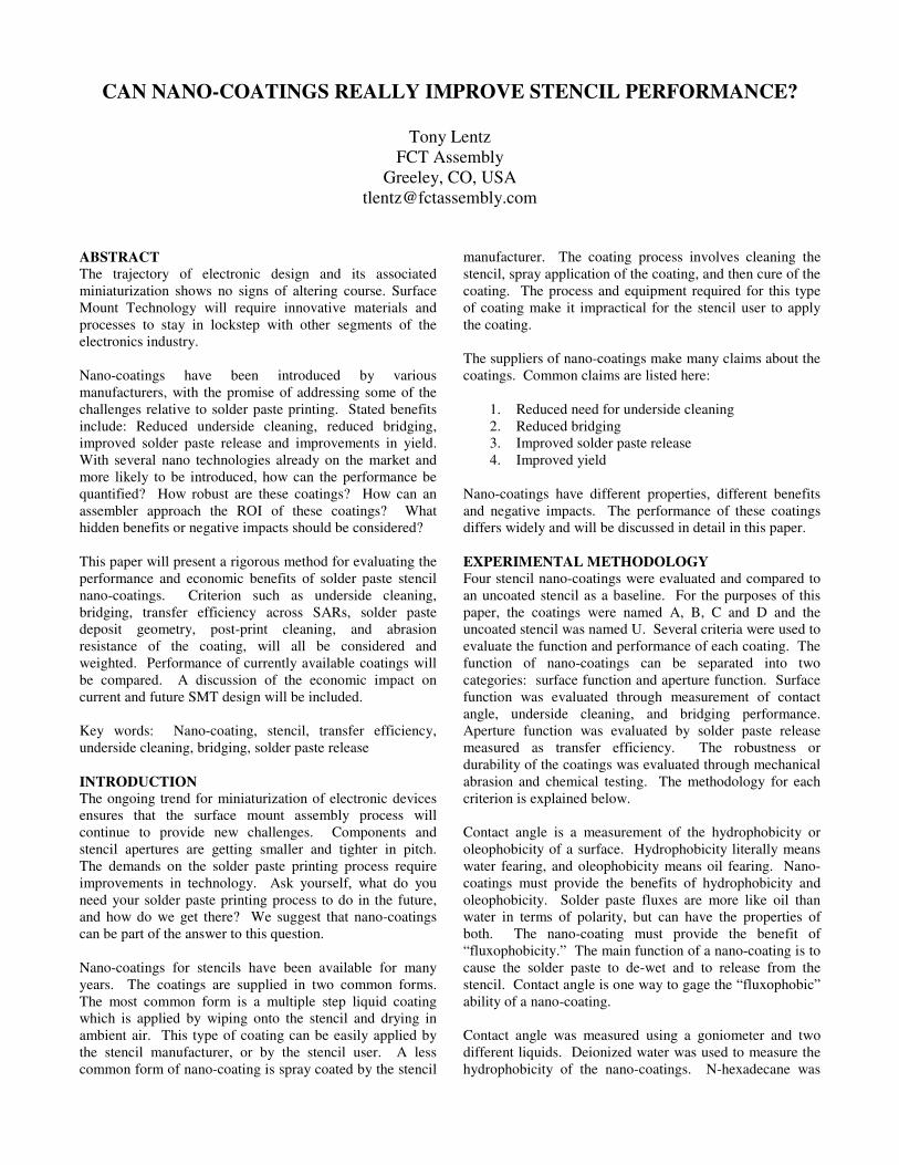
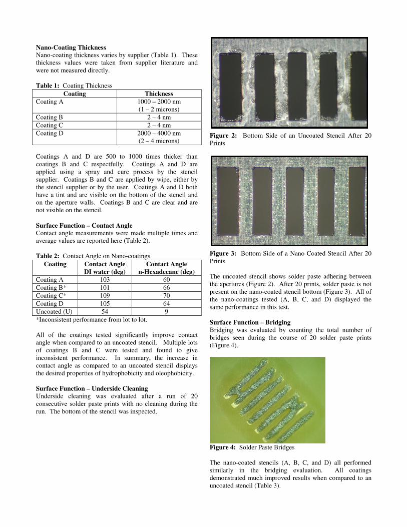
Underside cleaning was evaluated after a run of 20 consecutive solder paste prints with no cleaning during the run. The bottom of the stencil was inspected.
Figure 2: Bottom Side of an Uncoated Stencil After 20 Prints
Figure 3: Bottom Side of a Nano-Coated Stencil After 20 Prints The uncoated stencil shows solder paste adhering between the apertures (Figure 2). After 20 prints, solder paste is not present on the nano-coated stencil bottom (Figure 3). All of the nano-coatings tested (A, B, C, and D) displayed the same performance in this test. Surface Function – Bridging
Bridging was evaluated by counting the total number of bridges seen during the course of 20 solder paste prints (Figure 4).
Figure 4: Solder Paste Bridges The nano-coated stencils (A, B, C, and D) all performed similarly in the bridging evaluation. All coatings demonstrated much improved results when compared to an uncoated stencil (Table 3).
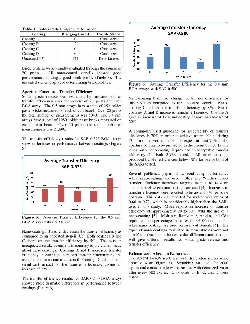
Table 3: Solder Paste Bridging Performance
Coating Bridging Count Profile Shape
Coating A 0 Consistent
Coating B 2 Consistent
Coating C 0 Consistent
Coating D 0 Consistent
Uncoated (U) 174 Deteriorates
Brick profiles were visually evaluated through the course of 20 prints. All nano-coated stencils showed good performance, holding a good brick profile (Table 3). The uncoated stencil displayed deteriorating brick profiles. Aperture Function – Transfer Efficiency
Solder paste release was evaluated by measurement of transfer efficiency over the course of 20 prints for each BGA array. The 0.5 mm arrays have a total of 252 solder paste bricks measured on each circuit board. Over 20 prints the total number of measurements was 5040. The 0.4 mm arrays have a total of 1080 solder paste bricks measured on each circuit board. Over 20 prints, the total number of measurements was 21,600. The transfer efficiency results for SAR 0.575 BGA arrays show differences in performance between coatings (Figure 5).
Figure 5: Average Transfer Efficiency for the 0.5 mm BGA Arrays with SAR 0.575 Nano-coatings B and C decreased the transfer efficiency as compared to an uncoated stencil (U). Both coatings B and C decreased the transfer efficiency by 5%. This was an unexpected result, because it is contrary to the claims made about these coatings. Coatings A and D increased transfer efficiency. Coating A increased transfer efficiency by 7% as compared to an uncoated stencil. Coating D had the most significant impact on the transfer efficiency, giving an increase of 22%. The transfer efficiency results for SAR 0.500 BGA arrays showed more dramatic differences in performance between coatings (Figure 6).
Figure 6: Average Transfer Efficiency for the 0.4 mm BGA Arrays with SAR 0.500 Nano-coating B did not change the transfer efficiency for this SAR as compared to the uncoated stencil. Nano-coating C reduced the transfer efficiency by 8%. Nano-coatings A and D increased transfer efficiency. Coating A gave an increase of 17% and coating D gave an increase of 22%. A commonly used guideline for acceptability of transfer efficiency is 70% in order to achieve acceptable soldering [3]. In other words, one should expect at least 70% of the aperture volume to be printed on to the circuit board. In this study, only nano-coating D provided an acceptable transfer efficiency for both SARs tested. All other coatings produced transfer efficiencies below 70% for one or both of the SARs tested. Several published papers show conflicting performance when nano-coatings are used. Shea and Whittier report transfer efficiency decreases ranging from 1 to 14% on stainless steel when nano-coatings are used [4]. Increases in transfer efficiency were reported to be around 1% for some coatings. This data was reported for surface area ratios of 0.66 to 0.77, which is considerably higher than the SARs used in this study. Moen reports an increase of transfer efficiency of approximately 20 to 30% with the use of a nano-coating [5]. Mohanty, Ramkumar, Anglin, and Oda report volume percentage increases for 01005 components when nano-coatings are used on laser cut stencils [6]. The types of nano-coatings evaluated in these studies were not specified. One should be aware that different nano-coatings will give different results for solder paste release and transfer efficiency. Robustness – Abrasion Resistance The ASTM D2486 scrub test with dry cotton shows some abrasion wear (Figure 7). Scrubbing was done for 2000 cycles and contact angle was measured with deionized water after every 500 cycles. Only coatings B, C, and D were tested.
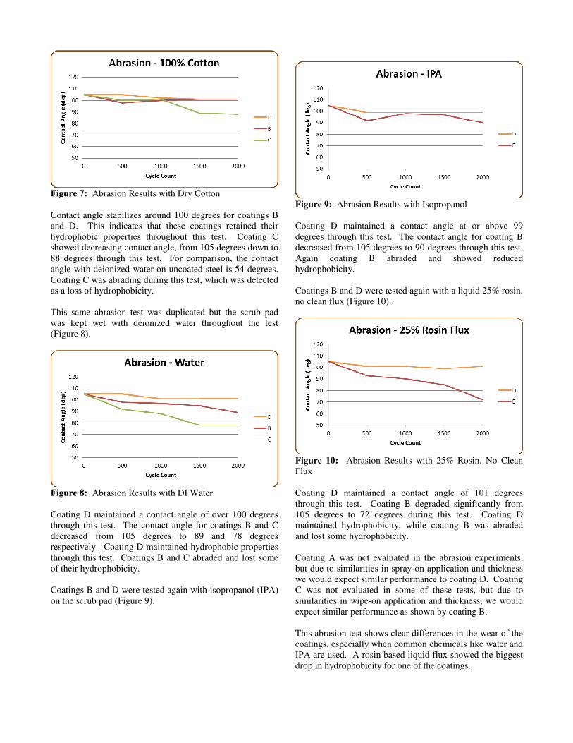
Figure 7: Abrasion Results with Dry Cotton Contact angle stabilizes around 100 degrees for coatings B and D. This indicates that these coatings retained their hydrophobic properties throughout this test. Coating C showed decreasing contact angle, from 105 degrees down to 88 degrees through this test. For comparison, the contact angle with deionized water on uncoated steel is 54 degrees. Coating C was abrading during this test, which was detected as a loss of hydrophobicity. This same abrasion test was duplicated but the scrub pad was kept wet with deionized water throughout the test (Figure 8).
Figure 8: Abrasion Results with DI Water Coating D maintained a contact angle of over 100 degrees through this test. The contact angle for coatings B and C decreased from 105 degrees to 89 and 78 degrees respectively. Coating D maintained hydrophobic properties through this test. Coatings B and C abraded and lost some of their hydrophobicity. Coatings B and D were tested again with isopropanol (IPA) on the scrub pad (Figure 9).
Figure 9: Abrasion Results with Isopropanol Coating D maintained a contact angle at or above 99 degrees through this test. The contact angle for coating B decreased from 105 degrees to 90 degrees through this test. Again coating B abraded and showed reduced hydrophobicity. Coatings B and D were tested again with a liquid 25% rosin, no clean flux (Figure 10).
Figure 10: Abrasion Results with 25% Rosin, No Clean Flux Coating D maintained a contact angle of 101 degrees through this test. Coating B degraded significantly from 105 degrees to 72 degrees during this test. Coating D maintained hydrophobicity, while coating B was abraded and lost some hydrophobicity. Coating A was not evaluated in the abrasion experiments, but due to similarities in spray-on application and thickness we would expect similar performance to coating D. Coating C was not evaluated in some of these tests, but due to similarities in wipe-on application and thickness, we would expect similar performance as shown by coating B. This abrasion test shows clear differences in the wear of the coatings, especially when common chemicals like water and IPA are used. A rosin based liquid flux showed the biggest drop in hydrophobicity for one of the coatings.
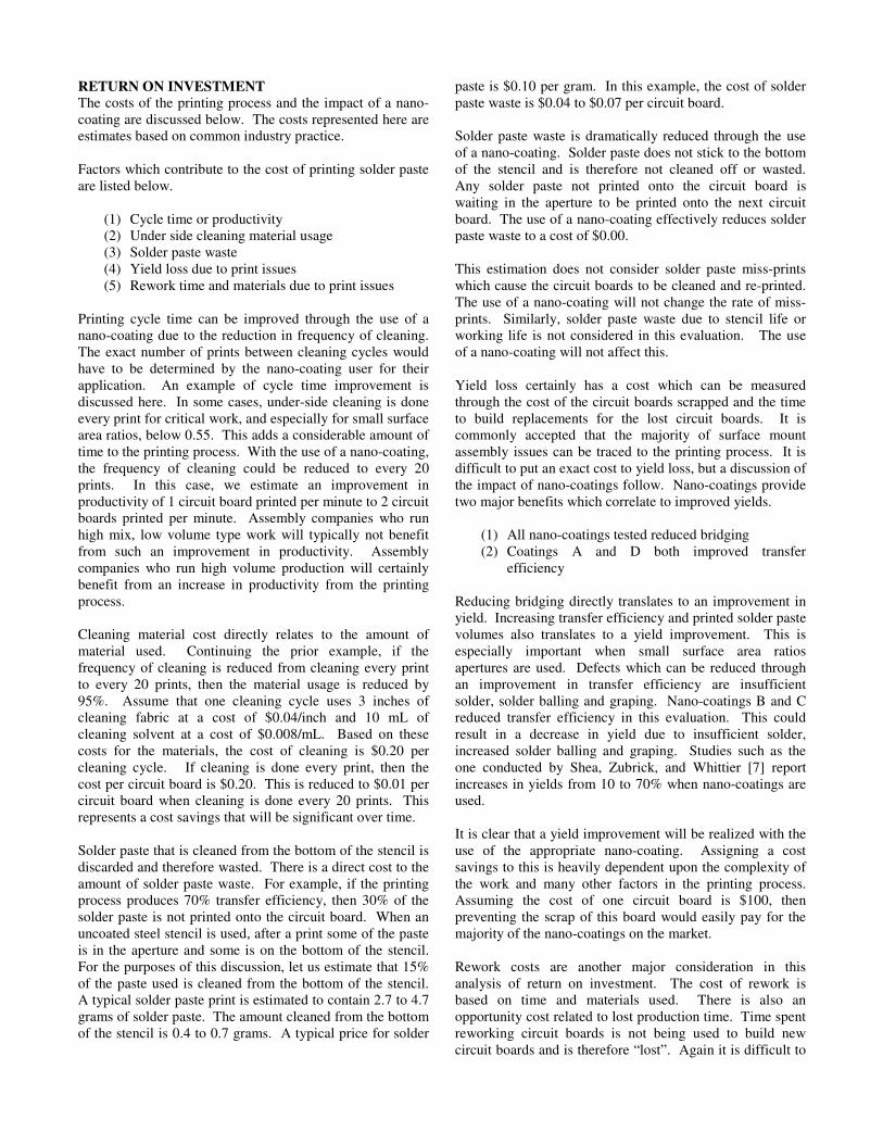
RETURN ON INVESTMENT
The costs of the printing process and the impact of a nano-coating are discussed below. The costs represented here are estimates based on common industry practice. Factors which contribute to the cost of printing solder paste are listed below.
(1) Cycle time or productivity (2) Under side cleaning material usage (3) Solder paste waste (4) Yield loss due to print issues (5) Rework time and materials due to print issues
Printing cycle time can be improved through the use of a nano-coating due to the reduction in frequency of cleaning. The exact number of prints between cleaning cycles would have to be determined by the nano-coating user for their application. An example of cycle time improvement is discussed here. In some cases, under-side cleaning is done every print for critical work, and especially for small surface area ratios, below 0.55. This adds a considerable amount of time to the printing process. With the use of a nano-coating, the frequency of cleaning could be reduced to every 20 prints. In this case, we estimate an improvement in productivity of 1 circuit board printed per minute to 2 circuit boards printed per minute. Assembly companies who run high mix, low volume type work will typically not benefit from such an improvement in productivity. Assembly companies who run high volume production will certainly benefit from an increase in productivity from the printing process. Cleaning material cost directly relates to the amount of material used. Continuing the prior example, if the frequency of cleaning is reduced from cleaning every print to every 20 prints, then the material usage is reduced by 95%. Assume that one cleaning cycle uses 3 inches of cleaning fabric at a cost of $0.04/inch and 10 mL of cleaning solvent at a cost of $0.008/mL. Based on these costs for the materials, the cost of cleaning is $0.20 per cleaning cycle. If cleaning is done every print, then the cost per circuit board is $0.20. This is reduced to $0.01 per circuit board when cleaning is done every 20 prints. This represents a cost savings that will be significant over time. Solder paste that is cleaned from the bottom of the stencil is discarded and therefore wasted. There is a direct cost to the amount of solder paste waste. For example, if the printing process produces 70% transfer efficiency, then 30% of the solder paste is not printed onto the circuit board. When an uncoated steel stencil is used, after a print some of the paste is in the aperture and some is on the bottom of the stencil. For the purposes of this discussion, let us estimate that 15% of the paste used is cleaned from the bottom of the stencil. A typical solder paste print is estimated to contain 2.7 to 4.7 grams of solder paste. The amount cleaned from the bottom of the stencil is 0.4 to 0.7 grams. A typical price for solder
paste is $0.10 per gram. In this example, the cost of solder paste waste is $0.04 to $0.07 per circuit board. Solder paste waste is dramatically reduced through the use of a nano-coating. Solder paste does not stick to the bottom of the stencil and is therefore not cleaned off or wasted. Any solder paste not printed onto the circuit board is waiting in the aperture to be printed onto the next circuit board. The use of a nano-coating effectively reduces solder paste waste to a cost of $0.00. This estimation does not consider solder paste miss-prints which cause the circuit boards to be cleaned and re-printed. The use of a nano-coating will not change the rate of miss-prints. Similarly, solder paste waste due to stencil life or working life is not considered in this evaluation. The use of a nano-coating will not affect this. Yield loss certainly has a cost which can be measured through the cost of the circuit boards scrapped and the time to build replacements for the lost circuit boards. It is commonly accepted that the majority of surface mount assembly issues can be traced to the printing process. It is difficult to put an exact cost to yield loss, but a discussion of the impact of nano-coatings follow. Nano-coatings provide two major benefits which correlate to improved yields.
(1) All nano-coatings tested reduced bridging (2) Coatings A and D both improved transfer
efficiency Reducing bridging directly translates to an improvement in yield. Increasing transfer efficiency and printed solder paste volumes also translates to a yield improvement. This is especially important when small surface area ratios apertures are used. Defects which can be reduced through an improvement in transfer efficiency are insufficient solder, solder balling and graping. Nano-coatings B and C reduced transfer efficiency in this evaluation. This could result in a decrease in yield due to insufficient solder, increased solder balling and graping. Studies such as the one conducted by Shea, Zubrick, and Whittier [7] report increases in yields from 10 to 70% when nano-coatings are used. It is clear that a yield improvement will be realized with the use of the appropriate nano-coating. Assigning a cost savings to this is heavily dependent upon the complexity of the work and many other factors in the printing process. Assuming the cost of one circuit board is $100, then preventing the scrap of this board would easily pay for the majority of the nano-coatings on the market. Rework costs are another major consideration in this analysis of return on investment. The cost of rework is based on time and materials used. There is also an opportunity cost related to lost production time. Time spent reworking circuit boards is not being used to build new circuit boards and is therefore “lost”. Again it is difficult to
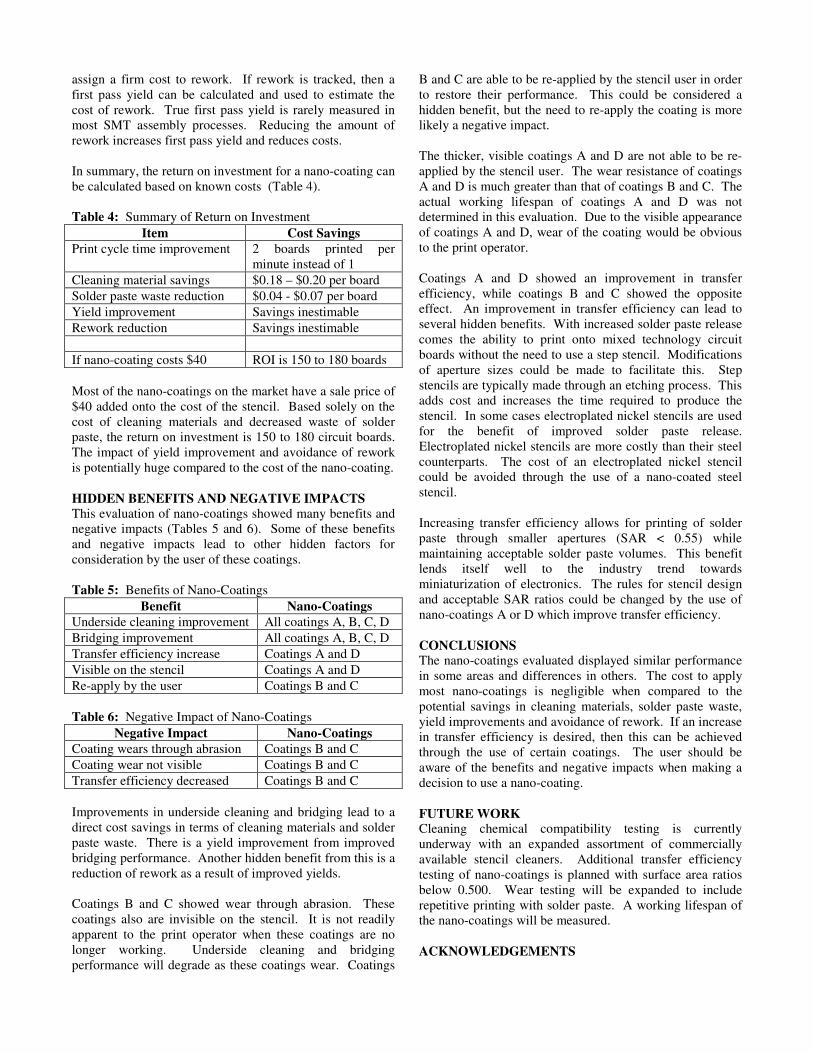
assign a firm cost to rework. If rework is tracked, then a first pass yield can be calculated and used to estimate the cost of rework. True first pass yield is rarely measured in most SMT assembly processes. Reducing the amount of rework increases first pass yield and reduces costs. In summary, the return on investment for a nano-coating can be calculated based on known costs (Table 4). Table 4: Summary of Return on Investment
Item Cost Savings
Print cycle time improvement 2 boards printed per minute instead of 1
Cleaning material savings $0.18 – $0.20 per board
Solder paste waste reduction $0.04 - $0.07 per board
Yield improvement Savings inestimable
Rework reduction Savings inestimable
If nano-coating costs $40 ROI is 150 to 180 boards
Most of the nano-coatings on the market have a sale price of $40 added onto the cost of the stencil. Based solely on the cost of cleaning materials and decreased waste of solder paste, the return on investment is 150 to 180 circuit boards. The impact of yield improvement and avoidance of rework is potentially huge compared to the cost of the nano-coating. HIDDEN BENEFITS AND NEGATIVE IMPACTS
This evaluation of nano-coatings showed many benefits and negative impacts (Tables 5 and 6). Some of these benefits and negative impacts lead to other hidden factors for consideration by the user of these coatings. Table 5: Benefits of Nano-Coatings
Benefit Nano-Coatings
Underside cleaning improvement All coatings A, B, C, D
Bridging improvement All coatings A, B, C, D
Transfer efficiency increase Coatings A and D
Visible on the stencil Coatings A and D
Re-apply by the user Coatings B and C
Table 6: Negative Impact of Nano-Coatings
Negative Impact Nano-Coatings
Coating wears through abrasion Coatings B and C
Coating wear not visible Coatings B and C
Transfer efficiency decreased Coatings B and C
Improvements in underside cleaning and bridging lead to a direct cost savings in terms of cleaning materials and solder paste waste. There is a yield improvement from improved bridging performance. Another hidden benefit from this is a reduction of rework as a result of improved yields. Coatings B and C showed wear through abrasion. These coatings also are invisible on the stencil. It is not readily apparent to the print operator when these coatings are no longer working. Underside cleaning and bridging performance will degrade as these coatings wear. Coatings
B and C are able to be re-applied by the stencil user in order to restore their performance. This could be considered a hidden benefit, but the need to re-apply the coating is more likely a negative impact. The thicker, visible coatings A and D are not able to be re-applied by the stencil user. The wear resistance of coatings A and D is much greater than that of coatings B and C. The actual working lifespan of coatings A and D was not determined in this evaluation. Due to the visible appearance of coatings A and D, wear of the coating would be obvious to the print operator. Coatings A and D showed an improvement in transfer efficiency, while coatings B and C showed the opposite effect. An improvement in transfer efficiency can lead to several hidden benefits. With increased solder paste release comes the ability to print onto mixed technology circuit boards without the need to use a step stencil. Modifications of aperture sizes could be made to facilitate this. Step stencils are typically made through an etching process. This adds cost and increases the time required to produce the stencil. In some cases electroplated nickel stencils are used for the benefit of improved solder paste release. Electroplated nickel stencils are more costly than their steel counterparts. The cost of an electroplated nickel stencil could be avoided through the use of a nano-coated steel stencil. Increasing transfer efficiency allows for printing of solder paste through smaller apertures (SAR < 0.55) while maintaining acceptable solder paste volumes. This benefit lends itself well to the industry trend towards miniaturization of electronics. The rules for stencil design and acceptable SAR ratios could be changed by the use of nano-coatings A or D which improve transfer efficiency. CONCLUSIONS The nano-coatings evaluated displayed similar performance in some areas and differences in others. The cost to apply most nano-coatings is negligible when compared to the potential savings in cleaning materials, solder paste waste, yield improvements and avoidance of rework. If an increase in transfer efficiency is desired, then this can be achieved through the use of certain coatings. The user should be aware of the benefits and negative impacts when making a decision to use a nano-coating. FUTURE WORK Cleaning chemical compatibility testing is currently underway with an expanded assortment of commercially available stencil cleaners. Additional transfer efficiency testing of nano-coatings is planned with surface area ratios below 0.500. Wear testing will be expanded to include repetitive printing with solder paste. A working lifespan of the nano-coatings will be measured. ACKNOWLEDGEMENTS
The author would like to thank Steve Johnson of Florida Cirtech for his work and guidance throughout this project. The author would also like to thank Bob Dervaes with FCT Assembly for his work on transfer efficiency and help with statistical evaluations. REFERENCES [1] ASTM D2486, “Standard Test Methods for Scrub Resistance of Wall Paints”, Reapproved 2012. [2] R. Dervaes, FCT Assembly, “Successful Stencil Printing: Performance is on the Surface”, 2013. [3] C. Ashmore, M. Whitmore, J. Schake, “Big Ideas on Miniaturization”, Proceedings of IPC Apex Expo, 2013. [4] C. Shea, R. Whittier, “Evaluation of Stencil Foil Materials, Suppliers and Coating”, Proceedings of SMTA International, 2011. [5] E. Moen, “Nano Coated Stencils for Optimized Solder Paste Printing”, Proceedings of Toronto SMTA Expo & Tech Forum, May 2012. [6] R. Mohanty, S. Ramkumar, C. Anglin, T. Oda, “Effect of Nano-Coated Stencil on 01005 Printing”, Proceedings of IPC Apex Expo, 2012. [7] C. Shea, M. Zubrick, R. Whittier, “Using SPI to Improve Print Yields”, Proceedings of SMTA International, 2011.