calculating and optimizing efficiency in lcd backlight drivers · · 2016-09-09calculating and...
TRANSCRIPT

1SNVA760–September 2016Submit Documentation Feedback
Copyright © 2016, Texas Instruments Incorporated
Calculating and Optimizing Efficiency in LCD Backlight Drivers
Application ReportSNVA760–September 2016
Calculating and Optimizing Efficiency in LCD BacklightDrivers
Cecilia Reyes, Sheng Jin
ABSTRACTBacklight displays have become the largest power consumer in mobile devices and personal electronics.When selecting components for an LED driver, efficiency is the most important consideration. The fivemain backlight driver components that generate the most power loss include: the boost inductor, switchingFET, Schottky diode, quiescent current, and headroom voltage. This application note will provide theequations to calculate power loss from these five main components along with comparing the trade-offs ofoptimizing each depending on preference. Calculations for power loss, as well comparison of trade-offs foroptimizing each component, are also provided.
Contents1 Basic Configuration of an LED Driver ..................................................................................... 22 Efficiency Calculations ...................................................................................................... 33 Component Optimization Trade-offs ...................................................................................... 44 Example....................................................................................................................... 75 Optimizing Efficiency Outside of the Boost Converter................................................................. 10
List of Figures
1 LCD Backlight Driver Configuration ....................................................................................... 22 Highlighted Power-Consuming Components ............................................................................ 33 Block Diagram for Switching Frequency Trade-offs .................................................................... 54 Block Diagram for Inductor Package Size Trade-offs................................................................... 55 Block Diagram for Inductance Trade-offs ................................................................................ 66 Block Diagram for Shottky Diode Size Trade-offs ....................................................................... 67 Block Diagram for Switching FET Size Trade-offs ...................................................................... 78 Typical Application Circuit of LM36272 ................................................................................... 89 Size Reference for the Tested Inductors ................................................................................. 910 LM36272 Boost Efficiency With 4.7-µH Inductor ........................................................................ 911 LM36272 Boost Efficiency With 10-µH Inductor ....................................................................... 1012 LM36272 Boost Efficiency With 15-µH Inductor ....................................................................... 1013 Various LED Configurations (1 × 8, 4 × 2, and 2 × 4)................................................................. 11
List of Tables
1 Calculating Power Loss from the Inductor................................................................................ 42 Calculating Power Loss from the Switching FET ........................................................................ 43 Calculating Power Loss from the Schottky Diode ....................................................................... 44 Calculating Power Loss from Quiescent Current ........................................................................ 45 Calculating Power Loss from the Headroom Voltage................................................................... 46 Recommended External Components .................................................................................... 8

Basic Configuration of an LED Driver www.ti.com
2 SNVA760–September 2016Submit Documentation Feedback
Copyright © 2016, Texas Instruments Incorporated
Calculating and Optimizing Efficiency in LCD Backlight Drivers
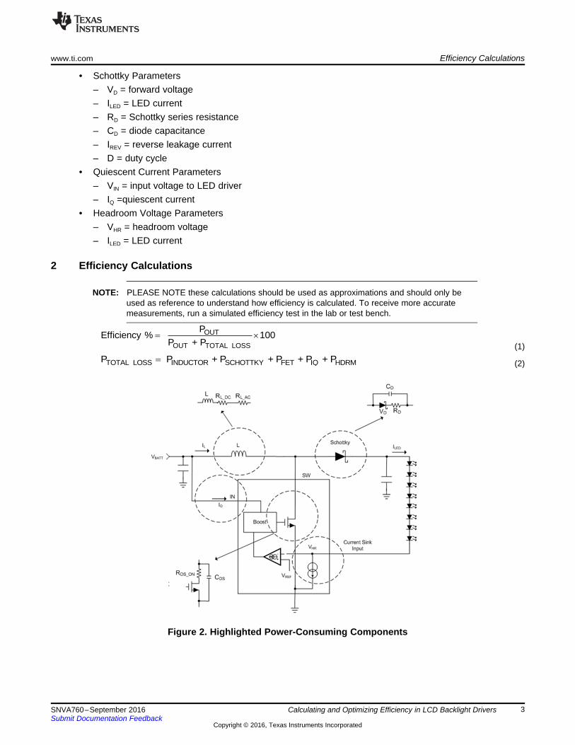
1 Basic Configuration of an LED DriverFigure 1 shows the basic configuration of an LCD driver while highlighting the five main power consumingcomponents.
Figure 1. LCD Backlight Driver Configuration
1.1 Necessary Parameters for Efficiency CalculationsThe following parameters are needed to calculate the power loss on each component:• Inductor RMS Parameters
– L = inductance– RLDCR = inductor DC resistance– IL = inductor current
• MOSFET Parameters– RSW = resistance of MOSFET switch– Cg = gate capacitance– CDS = drain-to-source capacitance– trise, tfall = rise and fall time of switch voltage– D = duty cycle; ratio of MOSFET on-time to period– ƒSW = switching frequency– IL = inductor current
TOTAL_LOSS INDUCTOR SCHOTTKY FET IQ HDRMP P + P + P + P + P
OUT
OUT TOTAL_LOSS
PEfficiency % 100
P + P u
www.ti.com Efficiency Calculations
3SNVA760–September 2016Submit Documentation Feedback
Copyright © 2016, Texas Instruments Incorporated
Calculating and Optimizing Efficiency in LCD Backlight Drivers
• Schottky Parameters– VD = forward voltage– ILED = LED current– RD = Schottky series resistance– CD = diode capacitance– IREV = reverse leakage current– D = duty cycle
• Quiescent Current Parameters– VIN = input voltage to LED driver– IQ =quiescent current
• Headroom Voltage Parameters– VHR = headroom voltage– ILED = LED current
2 Efficiency Calculations
NOTE: PLEASE NOTE these calculations should be used as approximations and should only beused as reference to understand how efficiency is calculated. To receive more accuratemeasurements, run a simulated efficiency test in the lab or test bench.
(1)
(2)
Figure 2. Highlighted Power-Consuming Components
HDRM HR LEDP V I u
IQ IN QP = V Iu
2CD D OUT SWP C V f u u
� �2RD L DP I R 1 D u u �
VD LED DP = I V (1 - D)u u
2CDS DS OUT SWP C V f u u
rise fallRD OUT IN SW1
P = (t + t ) V I f2
u u u u
2VD L DS(ON)P I R D u u
2 L(DC) L L(DCR)P I R u
Component Optimization Trade-offs www.ti.com
4 SNVA760–September 2016Submit Documentation Feedback
Copyright © 2016, Texas Instruments Incorporated
Calculating and Optimizing Efficiency in LCD Backlight Drivers
Table 1. Calculating Power Loss from the Inductor
POWER LOSS EQUATION LOSS TYPE
Inductor DC resistance (3) Conduction loss
Coreloss Power Look at inductor manufacturer's website Switching loss
Table 2. Calculating Power Loss from the Switching FET
POWER LOSS EQUATION LOSS TYPE
RDS(ON) (4) Conduction loss
Overlap power loss
(5)Switching loss
DC-capacitance loss (6) Switching loss
Table 3. Calculating Power Loss from the Schottky Diode
POWER LOSS EQUATION LOSS TYPE
Forward voltage power loss (7) Conduction loss
Diode resistance power loss (8) Conduction loss
Diode capacitance power loss (9) Switching loss
Table 4. Calculating Power Loss from Quiescent Current
POWER LOSS EQUATION LOSS TYPE
Quiescent current power loss (10) Conduction loss
Table 5. Calculating Power Loss from the Headroom Voltage
POWER LOSS EQUATION LOSS TYPE
Current sink headroom loss (11) Conduction loss
3 Component Optimization Trade-offsEvery consumer wants components with certain characteristics to fit the need of their solution. This portionof the applications note will highlight some common modifications in components and their tradeoffs.PLEASE NOTE that these are approximations and should be used as reference. The best way to seethese tradeoffs is testing LED drivers in lab with different components and comparing results.

www.ti.com Component Optimization Trade-offs
5SNVA760–September 2016Submit Documentation Feedback
Copyright © 2016, Texas Instruments Incorporated
Calculating and Optimizing Efficiency in LCD Backlight Drivers
3.1 Switching FrequencyIncreasing switching frequency allows customers to use smaller components for smaller solution sizes atthe expense of higher switching losses. Below is a block diagram showing the tradeoffs of increasing anddecreasing switching frequencies for the switching FET in the boost of an LCD driver.
Figure 3. Block Diagram for Switching Frequency Trade-offs
3.2 Inductor Package Size at Fixed InductanceFigure 4 shows the tradeoffs of different package sizes of inductors at a fixed inductance. As the packagesize increases, the cross-sectional area of the inductor also increases. This allows more current to flowthrough the inductor which then reduces the DCR.
Figure 4. Block Diagram for Inductor Package Size Trade-offs
3.3 Inductance at Fixed Package SizeFigure 5 shows the trade-offs when increasing the inductance at a fixed package size. Using the formula V= L (di/dt), it is clear that as inductance increases, the rate of change in current decreases. As inductancealso increases, the number of coils increases, therefore, increasing the resistance.

Component Optimization Trade-offs www.ti.com
6 SNVA760–September 2016Submit Documentation Feedback
Copyright © 2016, Texas Instruments Incorporated
Calculating and Optimizing Efficiency in LCD Backlight Drivers
Figure 5. Block Diagram for Inductance Trade-offs
3.4 Schottky Diode SizeAt larger package sizes, Schottky diodes reduce the forward drop and DC resistance but significantlyincreases the parasitic capacitance. This results to large switching losses and less efficient LED drivers.
Figure 6. Block Diagram for Shottky Diode Size Trade-offs

www.ti.com Component Optimization Trade-offs
7SNVA760–September 2016Submit Documentation Feedback
Copyright © 2016, Texas Instruments Incorporated
Calculating and Optimizing Efficiency in LCD Backlight Drivers
3.5 MOSFET Package SizeIn the case of an external switching FET, Figure 7 describes the tradeoffs between power loss and FETsize.
Figure 7. Block Diagram for Switching FET Size Trade-offs
4 ExampleReferencing the LM36272 LCD backlight driver, Figure 8 illustrates some of the calculations providedalong with a better understanding of the efficiency trade-offs that come with selecting components.

Example www.ti.com
8 SNVA760–September 2016Submit Documentation Feedback
Copyright © 2016, Texas Instruments Incorporated
Calculating and Optimizing Efficiency in LCD Backlight Drivers
Figure 8. Typical Application Circuit of LM36272
Table 6. Recommended External Components
DESIGNATOR DESCRIPTION VALUE EXAMPLEC1, C4, C5, C6, CFLY Ceramic capacitor 10 µF, 10 V C1608X5R0J106M
C2 Ceramic capacitor 1 µF, 35 V C2012X7R1H105K125ABL1 Inductor 4.7 µH, 1.94 A VLF504012MT-4R7ML1 Inductor 10 µH, 1.44 A VLF504015MT-100ML1 Inductor 15 µH, 1.25 A VLF504015MT-150ML2 Inductor 2.2 µH, 1.5 A DFE201612P-2R2MD1 Schottky diode 30 V, 500 mA NSR0530P2T5G
Table 6 shows examples of external components for the LM36272. The LM36272 requires a typicalinductance in the range of 4.7 µH to 15 µH. In this demonstration, the VLF504015MT-100M 10-µHinductor was used for the efficiency test. To highlight the effect of inductor selection on efficiency, thefollowing inductors were used to replace the inductor L1.
www.ti.com Example
9SNVA760–September 2016Submit Documentation Feedback
Copyright © 2016, Texas Instruments Incorporated
Calculating and Optimizing Efficiency in LCD Backlight Drivers
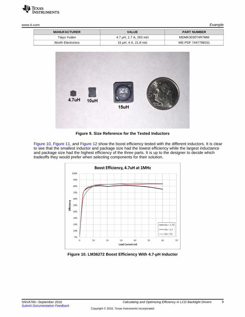
MANUFACTURER VALUE PART NUMBERTaiyo Yuden 4.7 µH, 1.7 A, 263 mΩ MDMK3030T4R7MM
Wurth Electronics 15 µH, 4 A, 21.8 mΩ WE-PDF 7447798151
Figure 9. Size Reference for the Tested Inductors
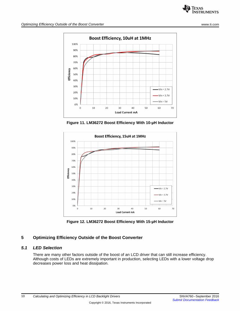
Figure 10, Figure 11, and Figure 12 show the boost efficiency tested with the different inductors. It is clearto see that the smallest inductor and package size had the lowest efficiency while the largest inductanceand package size had the highest efficiency of the three parts. It is up to the designer to decide whichtradeoffs they would prefer when selecting components for their solution.
Figure 10. LM36272 Boost Efficiency With 4.7-µH Inductor
Optimizing Efficiency Outside of the Boost Converter www.ti.com
10 SNVA760–September 2016Submit Documentation Feedback
Copyright © 2016, Texas Instruments Incorporated
Calculating and Optimizing Efficiency in LCD Backlight Drivers
Figure 11. LM36272 Boost Efficiency With 10-µH Inductor
Figure 12. LM36272 Boost Efficiency With 15-µH Inductor
5 Optimizing Efficiency Outside of the Boost Converter
5.1 LED SelectionThere are many other factors outside of the boost of an LCD driver that can still increase efficiency.Although costs of LEDs are extremely important in production, selecting LEDs with a lower voltage dropdecreases power loss and heat dissipation.
www.ti.com Optimizing Efficiency Outside of the Boost Converter
11SNVA760–September 2016Submit Documentation Feedback
Copyright © 2016, Texas Instruments Incorporated
Calculating and Optimizing Efficiency in LCD Backlight Drivers
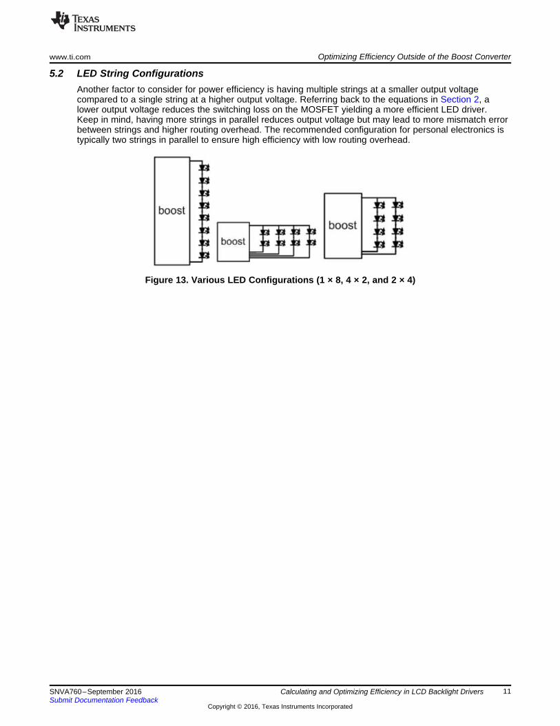
5.2 LED String ConfigurationsAnother factor to consider for power efficiency is having multiple strings at a smaller output voltagecompared to a single string at a higher output voltage. Referring back to the equations in Section 2, alower output voltage reduces the switching loss on the MOSFET yielding a more efficient LED driver.Keep in mind, having more strings in parallel reduces output voltage but may lead to more mismatch errorbetween strings and higher routing overhead. The recommended configuration for personal electronics istypically two strings in parallel to ensure high efficiency with low routing overhead.
Figure 13. Various LED Configurations (1 × 8, 4 × 2, and 2 × 4)

IMPORTANT NOTICE
Texas Instruments Incorporated and its subsidiaries (TI) reserve the right to make corrections, enhancements, improvements and otherchanges to its semiconductor products and services per JESD46, latest issue, and to discontinue any product or service per JESD48, latestissue. Buyers should obtain the latest relevant information before placing orders and should verify that such information is current andcomplete. All semiconductor products (also referred to herein as “components”) are sold subject to TI’s terms and conditions of salesupplied at the time of order acknowledgment.TI warrants performance of its components to the specifications applicable at the time of sale, in accordance with the warranty in TI’s termsand conditions of sale of semiconductor products. Testing and other quality control techniques are used to the extent TI deems necessaryto support this warranty. Except where mandated by applicable law, testing of all parameters of each component is not necessarilyperformed.TI assumes no liability for applications assistance or the design of Buyers’ products. Buyers are responsible for their products andapplications using TI components. To minimize the risks associated with Buyers’ products and applications, Buyers should provideadequate design and operating safeguards.TI does not warrant or represent that any license, either express or implied, is granted under any patent right, copyright, mask work right, orother intellectual property right relating to any combination, machine, or process in which TI components or services are used. Informationpublished by TI regarding third-party products or services does not constitute a license to use such products or services or a warranty orendorsement thereof. Use of such information may require a license from a third party under the patents or other intellectual property of thethird party, or a license from TI under the patents or other intellectual property of TI.Reproduction of significant portions of TI information in TI data books or data sheets is permissible only if reproduction is without alterationand is accompanied by all associated warranties, conditions, limitations, and notices. TI is not responsible or liable for such altereddocumentation. Information of third parties may be subject to additional restrictions.Resale of TI components or services with statements different from or beyond the parameters stated by TI for that component or servicevoids all express and any implied warranties for the associated TI component or service and is an unfair and deceptive business practice.TI is not responsible or liable for any such statements.Buyer acknowledges and agrees that it is solely responsible for compliance with all legal, regulatory and safety-related requirementsconcerning its products, and any use of TI components in its applications, notwithstanding any applications-related information or supportthat may be provided by TI. Buyer represents and agrees that it has all the necessary expertise to create and implement safeguards whichanticipate dangerous consequences of failures, monitor failures and their consequences, lessen the likelihood of failures that might causeharm and take appropriate remedial actions. Buyer will fully indemnify TI and its representatives against any damages arising out of the useof any TI components in safety-critical applications.In some cases, TI components may be promoted specifically to facilitate safety-related applications. With such components, TI’s goal is tohelp enable customers to design and create their own end-product solutions that meet applicable functional safety standards andrequirements. Nonetheless, such components are subject to these terms.No TI components are authorized for use in FDA Class III (or similar life-critical medical equipment) unless authorized officers of the partieshave executed a special agreement specifically governing such use.Only those TI components which TI has specifically designated as military grade or “enhanced plastic” are designed and intended for use inmilitary/aerospace applications or environments. Buyer acknowledges and agrees that any military or aerospace use of TI componentswhich have not been so designated is solely at the Buyer's risk, and that Buyer is solely responsible for compliance with all legal andregulatory requirements in connection with such use.TI has specifically designated certain components as meeting ISO/TS16949 requirements, mainly for automotive use. In any case of use ofnon-designated products, TI will not be responsible for any failure to meet ISO/TS16949.
Products ApplicationsAudio www.ti.com/audio Automotive and Transportation www.ti.com/automotiveAmplifiers amplifier.ti.com Communications and Telecom www.ti.com/communicationsData Converters dataconverter.ti.com Computers and Peripherals www.ti.com/computersDLP® Products www.dlp.com Consumer Electronics www.ti.com/consumer-appsDSP dsp.ti.com Energy and Lighting www.ti.com/energyClocks and Timers www.ti.com/clocks Industrial www.ti.com/industrialInterface interface.ti.com Medical www.ti.com/medicalLogic logic.ti.com Security www.ti.com/securityPower Mgmt power.ti.com Space, Avionics and Defense www.ti.com/space-avionics-defenseMicrocontrollers microcontroller.ti.com Video and Imaging www.ti.com/videoRFID www.ti-rfid.comOMAP Applications Processors www.ti.com/omap TI E2E Community e2e.ti.comWireless Connectivity www.ti.com/wirelessconnectivity
Mailing Address: Texas Instruments, Post Office Box 655303, Dallas, Texas 75265Copyright © 2016, Texas Instruments Incorporated