ca-i , o q - nasa · ca-i , o q mcr-90-536 contract no. nas8-36583 ... ac remote controlled circuit...
TRANSCRIPT

ca-i , o qMCR-90-536Contract No. NAS8-36583
Final
Report July 1990
Space StationCommon Module
Network Topologyand Hardware
Development
: g" : D
DcV_LOPMLNT Find| k,.-',_.or_ ('44rtin _ _r i_.tc _
C o • _.. ) _'? =_ r C ? ,'.;I ? ,'_
https://ntrs.nasa.gov/search.jsp?R=19910005060 2018-09-02T19:54:05+00:00Z

I
.....j,
-.__.J

\ MCR-90-536Contract No. NAS8-36583
Final
Report
July 1990
SPACE STATIONCOMMON MODULE NETWORK TOPOLOGY
AND HARDWARE DEVELOPMENT
authorP. Anderson
Other Con tribu tors
L. BraunagelS. ChwirkaM. FishmanK. Freeman
D. EasonD. LandisL. Lech
J. MartinJ. McCorkle
W. MillerC. Pistole
S. VanWormer
Martin Marietta Astronautics GroupP.O. Box 179
Denver, Colorado 80201

!
z

MCR-90-536Final
FOREWARD Report July 1990
This report was prepared by Martin Marietta Denver Astronautics Group for the National
Aeronautics and Space Administration, George C. Marshall Space Flight Center (NASA/MSFC),
in response to contract NAS8-36583. This Final Report is submitted to the Electrical Power
Branch at NASA/MSFC as specified in the contract data requirements list.
FOREWARD
i

TABLE OF CONTENTSFinal
Report
MCR-90-536
July 1990
3.0
4.0
5.0
2.1
2.2
2.3
2.4
3.1
4.1
4.2
4.3
4.4
4.5
4.6
4.7
4.8
4.9
4.10
4.11
4.12
4.13
4.14
4.15
4.16
5.1
5.2
5.3
5.4
5.5
5.6
INTRODUCTION
TASK I SSM/PMAD PRELIMINARY DEFINITION
SSM/PMAD Requirements Definition
Loads Analysis
Conceptual Network Layouts
Network Concept Selection
TASK II - HARDWARE SELECTION
Technology Readiness Assessment
TASK HI - ADVANCED HARDWARE DEVELOPMENT
Switchgear Interface Controller
Generic Controller Card
Analog to Digital Card
AC Remote Power Controller
AC Remote Controlled Circuit Breaker
AC Remote Bus Isolator
AC Voltage Sensor
AC Current Sensors
Temperature Sensors
DC Remote Power Controller
DC Remote Controlled Circuit Breaker
DC Remote Bus Isolator
DC Voltage Sensor
DC Current Sensors
Card Cage
Test Tool
TASK/V - SSM/PMAD TESTING
Switchgear Interface Controller
Generic Controller Card
Analog to Digital Card
AC Remote Power Conn'oUer
AC Remote Controlled Circuit Breaker
AC Remote Bus Isolator
1-1
2-1
2-1
2-1
2-1
2-7
3-1
3-1
4-1
4-1
4-3
4-15
4-20
4-24
4-25
4-26
4-27
4-28
4-30
4-32
4-34
4-34
4-36
4-37
4-37
5-1
5-1
5-1
5-2
5-2
5-3
5-4
TABLE OF CONTENTS
ii


TABLE OFCONTENTSFinal
Report
MCR-90-536
July 1990
6.0
7.08.0
9.010.0
5.7
5.8
5.9
5.10
5.11
5.12
5.13
5.14
5.15
5.16
AC VoltageSensorAC CurrentSensors
TemperatureSensorsDC RemotePowerControllerDC RemoteControlledCircuitBreaker
DC RemoteBusIsolator
DC VoltageSensorDC CurrentSensors
CardCageLoadConverterAPPENDIXI - SWlTCHGEARTECHNOLOGYASSESSMENT__
APPENDIX rI - SIC TO LLP INTERFACE DOCUMENT
APPENDIX III - 20 KHZ AC RPC SPECIFICATIONS
APPENDIX IV - DC RCCB PRODUCT CONTROL DOCUMENT __
APPENDIX V - DC - 400 HZ LOAD CONVERTER REPORT
5-4
5-4
5-4
5-5
5-5
5-5
5-6
5-6
5-7
5-7
I-1
1I-1
III-1
IV-1
V-1
TABLE OF CONTENTS
111

i

FIGURES
Final
Report
MCR-90-536
July 1990
2.3-1
2.3-2
2.3-3
2.3-4
2.4-1
2.4-2
4.1.2-1
4.2.2-1
4.2.2-2
4.2.2-3
4.2.2-4
4.2.2-5
4.2.4-1
4.2.4-2
4.2.4-3
4.2.4-4
4.3.2-1
4.4.2-1
4.5.2-1
4.7.2-1
4.8.2-1
4.8.2-2
4.10.2-1
4.11.2-1
4.12.2-1
4.13.2-1
4.14.2-1
4.15-1
5.4-1
5.10-1
1.1-1
Option 1 Breadboard
Option 2 Breadboard
Option 3 Breadboard
Option 4 Breadboard
Ring Bus Configuration
Star Bus Configuration
Switchgear Interface Controller Card
Generic Controller Card
GC Card Analog Processors
Generic Card Switch Status Circuitry
Generic Card Configurations
GC Card State Machine
DC-Generic Controller Card
GC Card Analog Processors
Generic Card Switch Status Circuitry
DC-GC Card State Machine
Analog to Digital Card
AC Remote Power Controller
AC Remote Controlled Circuit Breaker
AC Voltage Sensor
AC Current Sensor
50 mA Current Sensor
DC Remote Power Controller
DC Remote Controlled Circuit Breaker
AC/DC Remote Bus Isolator
DC Voltage Senser
DC Current Sensor
Card Cage
AC RPC Fast Trip
DC RPC Fast Trip
Switchgear Technology Assessment
2-9
2-10
2-11
2-12
2-13
2-14
4-2
4-6
4-7
4-8
4-8
4-11
4-12
4-13
4-14
4-16
4-19
4-21
4-25
4-27
4-28
4-28
4-31
4-33
4-35
4-35
4-36
4-38
5-3
5-6
1-2
FIGURES
iv


TABLESFinal
Report
MCR-90-536
July 1990
2.1-1
2.2-1
3.2-1
4.2.1-1
4.2.1-2
4.2.2-1
4.2.2-2
4.2.4-1
4.3.1-1
4.4.2-1
4.2-2
4.8.1-1
4.9.1-1
4.14.1-1
4.15-1
5.16-1
5.16-2
SSM/PMAD Requirements
Space Station Loads Data Base
MSFC Breadboard Hardware
GC Card Truth Table Requirements
GC Card Processor Trip Level Requirements
Analog Signal Processors
Switch Configuration Lines and Descriptions
DC-GC Analog Signal Processor
Required A/D Card Sensor Inputs, Processors, and Ranges
RPC Analog Data Given to the GC Card
RPC Housekeeping Power Supplies and Loads
AC Current Sensor Requirements
Temperature Sensor Requirements
DC Current Sensor Requirements
Card Cage Hardware Requirements
Load Converter Design Goals
Load Converter Technologies
Pa_w 2-2
2-4
3-2
4-4
4-4
4-5
4-9
4-12
4-15
4-23
4-23
4-27
4-29
4-36
4-37
5-7
5-7
TABLES
V


ACRONYMNSFinal
Report
MCR-90-536
July 1990
A
A/D
AC
COR
DC
EPS
GC
GFP
GND
I-IZ
I2t
LLP
MMAG
MSFC
NASA
PDCU
RBI
RCCB
RPC
SIC
SPST
SSM/PMAD
SOW
V
W
Amps
Analog to Digital
Alternating Current
Contracting Office Representative
Direct Current
Electrical Power System
Generic Controller
Ground Fault Protection
Ground
Hertz (Cycles/Second)
Product of Current Squared and Time
Lowest Level Processor
Martin Marietta A,,tronautics Group
George C. Marshall Space Flight Center
National Aeronautics and Space Administration
Power Distribution Control Unit
Remote Bus Isolator
Remote Controlled Circuit Breaker
Remote Power Controller
Switchgear Interface Controller
Single Pole Single Throw
Space Station Module Power Management and Distribution
Statement of Work
Volts
Watts
ACRONYMNS
vi

, J
-w..r--

INTRODUCTION
MCR-90-536Final
Report July 1990
_ 1.0 INTRODUCTION
This document reports on Contract NAS8-36583 and is in response to the work which was
performed in developing and delivering hardware for the Space Station Common Module Network
Topology and Hardware Development contract. This work was performed by Martin Marietta
Corporation, Denver Astronautics Group for the National Aeronautics and Space Administration,
George C. Marshall Space Fhght Center, in support of the Electrical Power Branches'
development of an automated power distribution system test bed. The NASA Contracting
Officer's technical representative for the contract is Ms. Cindy Thomason. Martin Marietta is
r"',orting on Tasks I, II, III, and IV of the contract.
Task I
Task II
Task III
Task IV
Common Module Power Management and Distribution System Preliminary
Definition
Hardware Selection
Hardware Advanced Development and Verification Test
Common Module Power Management and Distribution Breadboard Testing
INTRODUCTION
1-1


TASKI
MCR-90-536Final
Report July 1990
2.0 TASK I
Space Station Common Module Power Man aeement and Distribution System Preliminary Definition
The purpose of Task I was to develop conceptual Space Station Common Module Power
Management and Distribution (SSM/PMAD) network layouts, develop detailed network
evaluations, and to identify individual pieces of hardware to be developed for the SSM/PMAD test
bed.
2.1 SSM/PMAD Requirements D¢finition
The requirements in the Statement of Work (SOW), the Martin Marietta Astronautics Group
(MMAG) SSM/PMAD requirements, the former revision of the Space Station Reference
Configuration Description, and tae space station system efforts as defined in the C2, C3 and C4
specifications were analyzed and used to develop a set of baseline SSM/PMAD requirements.
These requirements were reviewed with the Marshall Space Flight Center (MSFC) Contracting
Officer Representative (COR) early in the program and are listed in Table 2.1-1.
2.2 Loads Analysis
A space station loads data base was developed from a previously existing space station
loads analysis data base as reflected in Table 2.2-1. This provided a point of departure to develop
switchgear current carrying requirements.
2.3 Conceptual Network Layouts
Conceptual network layo_,ts were developed based on functional, configuration and energy
storage candidate networks as supplied by MSFC. Several ground rules were established which
were taken into account in developing the conceptual layouts:
o Redundancy - a) Each load will have a minimum of two paths back to the primary
power source; b) redundancy will be implemented to such a degree as to identify all
TASKI
2-1

Table 2.1-1 CM/PMAD Requirements
o
.
.
.
.
o
.
.
.
10.
11.
12.
13.
14.
15.
16.
l_eo_uiremerg
The CM EPS shall convert and condition primary distribution systempower to the types best suited for distribution. Within the CM, thepower shall be distributed, monitored, circuit protected andcontrolled. Power networks shall be provided for all avionics.
Accept power from redundant utility buses. Loss of onefunctional path will not result in the loss of the alternate redundantpath.
Diverse routing of redundant wiring and equipment shall be
implemented.
The design shall preclude a single open circuit causing loss of thebus.
The design shall provide ve,_cation of redundancy without ORUremoval.
The EPS shall provide both redundancy status and management.
Redundant accommodations for complete command and controlshall be provided in separate locations.
A means of selecfing/deselecting prime power buses and loadsshall be provided.
Power sources and distribution shall be protected against over-loads and faults.
All wiring shall be protected at the source or be current limited.
All circuit protection devices shall be resettable or replaceable.
Ground fault protection shall be provided on circuits that areaccessible.
The design shall preclude failure propagation.
All equipment shall be easily removed and replaced at the ORU level.
The system shall be capable of undergoing maintenance withoutinterruption of critical services or other SSPE operations.
Maintenance shall not cause hazardous or destructive conditions.
Source
Document/
SS-SRD-100/2.2.3.1
C-4/2.1.10.4
C-4/2.2.3.h
C-4/2.2.3.h
SS-SRD- 100/2.1.11.4.b
C-4/2.2.3.f
C-4/2.2.3.e
C-4/2.2.3.h
C-4/2.2.3.h
C-4/2.1.11.2.k
C-4/2.1.10.3
C-3/3.2.a
C-4/2.1.9.d
C-4/2.1.9.g
TASK I
2-2
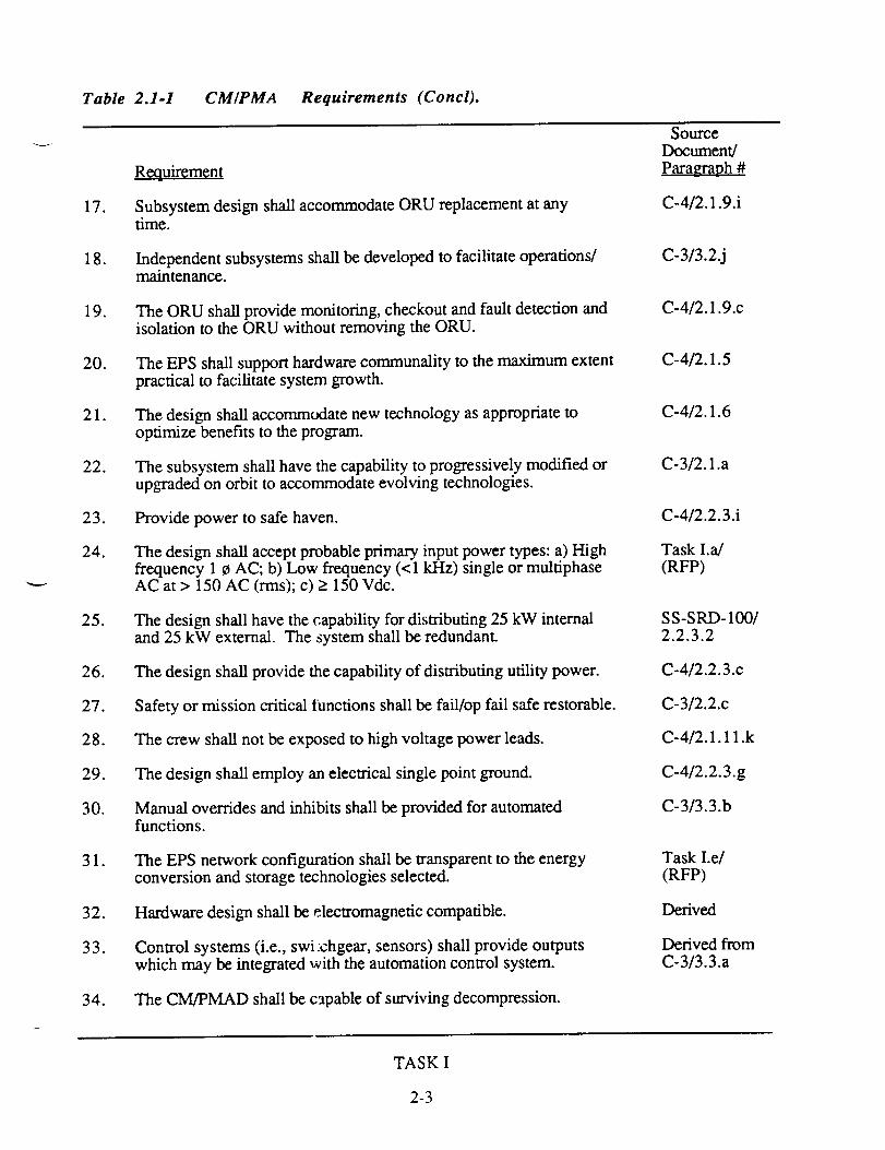
Table 2.1-1 CM/PMA Requirements (Concl).
17.
18.
19.
20.
21.
22.
25.
26.
27.
28.
29.
30.
31.
34.
Requirement
Subsystem design shall accommodate ORU replacement at anytime.
Independent subsystems shall be developed to facilitate operations/maintenance.
The ORU shall provide monitoring, checkout and fault detection andisolation to the ORU without removing the ORU.
The EPS shall support hardware communality to the maximum extentpractical to facilitate system growth.
The design shall accommodate new technology as appropriate tooptimize benefits to the program.
The subsystem shall have the capability to progressively modified orupgraded on orbit to accommodate evolving technologies.
Provide power to safe haven.
The design shall accept probable primary input power types: a) Highfrequency 1 ¢ AC; b) Low frequency (<1 kHz) single or multiphaseAC at > 150 AC (rms); c) _> 150 Vdc.
The design shall have the capability for distributing 25 kW internaland 25 kW external. The system shall be redundant.
The design shall provide the capability of distributing utility power.
Safety or mission critical functions shall be fail/op fail safe restorable.
The crew shall not be exposed to high voltage power leads.
The design shall employ an electrical single point ground.
Manual overrides and inhibits shall be provided for automatedfunctions.
The EPS network configuration shall be transparent to the energyconversion and storage technologies selected.
Hardware design shall be electromagnetic compatible.
Control systems (i.e., swi :chgear, sensors) shall provide outputswhich may be integrated with the automation control system.
The CM/PMAD shall be capable of surviving decompression.
Source
Document/
Para_m'aph #
C- 4/2.1.9.i
C-3/3.2.j
C-4/2.1.9.c
C- 4/2.1.5
C-4/2.1.6
C-3/2.1.a
C-4/2.2.3.i
Task I.a/(RFP)
SS-SRD- 100/2.2.3.2
C-4/2.2.3.c
C-3/2.2.c
C-4/2.1.11 .k
C-4/2.2.3.g
C-3/3.3.b
Task I.e/(RFP)
Derived
Derived fromC-3/3.3.a
TASKI
2-3

Table 2.2-1 Space Station Loads Data Base
SUBASSY NOMINAL DUTYCYCL MIL
C02 RemovalC02 Reduction02 Generation
Urine Hygiene ProcessingUrine Hygiene ProcessingPotable Water Processi,,gPotable Water ProcessingH20 Storage & DistributionTrash Coll. & ProcessingPropellant TanksPressure TransducersPressure Transducers
Propellant TanksPressure Transducers
Propellant TanksPressure Transducers
Battery/Charger-Log-0-
Sputtering Deposition UnitMass Measurement SystemMetallographic MicroscopeX-ray Topography UnitUV/VIS/NIR SpectrometerOptical MicroscopeLow Speed CentrifugeHall Probe
Auto. Cut & Polishing UnitHi-Perf. Liq. ChromatographScanning Electron Mierosc.Fourier Tmsfrm IR Spect.Gas Chromgph-Mass Spectro.Elec Conductivity ProbeBattery ChargerLiq./Solid Seperation Sys.Fluids Glovebox
Master Computer3-Axis Rec. Accelerometer
Freeze DrierVideo Facilities
Waster Disposal System-0-
-0-
-0-
Annunciator UnitRemote Annunciator
Mag Disk (600 MBIT)
Mag Tape (1000 GBIT)Bus Interface Units
Gateway Interface Unit
157.000294.0001597.0040.0000550.000550.00020.00003.0000015.000012.00000.600000.6000012.00000.6000012.00000.6000035 ?00080.00001700.00100.000200.0001500.00250.00050.0000250.000500.000750.0002500.001500.00750.0004000.00150.00020.0000200.000200.0001000.0050.0000500.000100.000750.000150.000
300.000150.0005.00000i .00000_0.000010.00005.00000'.0.0000
HB1 HB2 LOG
1.00000 1 1 1 -0-1.00000 1 1 1 -0-1.00000 1 1 1 -0-
-0- -0- 1 1 -0-1.00000 -0- 1 1 -0-1.00000 1 1 -0- -0-1.00000 1 1 1 -0-
-0- -0- 1 1 -0-1.00000 -0- 1 -0- 10.50000 -0- -0- -0- -0-1.00000 -0- -0- -0- -0-1.00000 -0- -0- -0- -0-0.50000 -0- -0- -0- 31.00000 -0- -0- -0- 70.50000 -0- -0- -0- -0-1.00000 -0- -0- -0- 71.00000 -0- -0- -0- 21.00000 -0- -0- -0- -0-0.08000 1 -0- -0- -0-0.16000 1 -0- -0- -0-0.16000 1 -0- -0- -0-0.16000 1 -0- -0- -0-0.16000 1 -0- -0- -0-0.25000 1 -0- -0- -0-0.33000 1 -0- -0- -0-0.16000 1 -0- -0- -0-0.42000 1 -0- -0- -0-0.16000 1 -0- -0- -0-0.25000 1 -0- -0- -0-0.25000 1 -0- -0- -0-0.16000 1 -0- -0- -0-0.04000 1 -0- -0- -0-0.50000 1 -0- -0- -0-0.08000 1 -0- -0- -0-0.25000 1 -0- -0- -0-1.013000 1 -0- -0- -0-1.00000 1 -0- -0- -0-0.08000 1 -0- -0- -0-0.33000 1 -0- -0- -0-0.50000 1 -0- -0- -0-0.01000 2 2 2 20.37500 -0- 1 -0- -0-0.04160 1 1 1 10,01000 2 1 1 -0-0.01000 1 3 3 40.50000 3 2 2 -0-0.50000 1 1 1 -0-1.00000 55 14 14 121.00000 3 2 2 2
LSL
111
-0-
-0-
-0-
1-0-
-0-
-0-
-0-
-0-
-0-
0-0-
-0-
-0-
-0-
-0-
-0-
-0-
-0-
-0-
-0-
-0-
-0-
-0-
-0-
-0-
-0-
-0-
-0-
-0-
-0-
-0-
-0-
-0-
-0-
-0-
-0-
2-0-
11332162
TASK I
2-4

Table 2.2-1 Space Station Loads Data Base (Cont'd)
SUBASSY NOMINAL DUTYCYCL MIL
Subsystem ControllerDedicated ControllerCirculation Fan
Cabin Fan PackageTemp ControllerBulk Storage FreezerFreezer
02/N2 Pressure ControllerVent & Relief
Primary Power Dist. Assy.Secondary Distrib. Assy.Subsystem Load CenterExterior Light ControllerInt. Light ControllerEmergency Lighting-0-
-0-
-0-
-0-
Pump PackageControl ValvesPressure SensorFlow Meter
Pump PackageControl ValvePressure SensorsFlow Meter
Ext. Power Condition AssyExt. DC Power ConditioningValve Drive Amp AssyPower Condition AssyParticulate Glovebox
Data Recording UnitH20 Detonizer/DepyrogenizUV Sterilization OvenPort. UV Sterilization Ut
Optical PyrometerDig. Reading OscilloscopeStereo MacroscopeFreezer
RefrigeratorLatex Reactor SystemProtein Crystal Growth FCDirect Solidification Fur
Droplet Combustion Facil.Controlled Atmosphere Fur
Electrophoresis FacilityVapor Crystal Growth FurAcoustic Contrless Pr Fac
30.0000 1.00000 2350.0000 1.00000 36650.000 1.00000 1730.000 1.00000 231.0000 1.00000 2495.000 0.50000 -0-495.000 0.50000 -0-
30.0000 1.00000 117.0000 0.01000 120.0000 1.00000 220.0000 1.00000 220.0000 1.00000 310.0000 1.00000 4220.000 0.67000 220.0000 1.00000 28.40000 0.20000 220.0000 1.00000 442.0000 1.00000 135.0000 0.20000 1'!76.000 1.00000 269.0000 1.00000 190.84000 1.00000 40.84000 1.00000 8371.000 1.00000 292.0000 1.00000 10.84000 1.00000 20.84000 1.00000 430.0000 1.00000 -0-30.0000 1.00000 -0-45.0000 1.00000 -0-20.0000 1.00000 4250.000 0.75000 1100.000 1.00000 13000.00 0.50000 1150.000 0.08000 1100.000 0.08000 120.0000 0.08000 1100.000 0.50000 1_.0.0000 0.08000 1500.000 1.00000 1300.000 1.00000 1100.000 1.00000 1500.000 0.75000 115000.0 0.83000 1500.000 0.16000 13500.00 0.50000 13000.00 0.75000 12000.00 0.83000 15000.00 0.50000 1
HB1
1454122
-0 o
1112234222214214262124
°0 °
-0-
-0 °
2-0-
-0-
-0-
-0-
°0-
°0-
-0-
-0-
°0 °
°0-
-0-
-0-
-0-
-0 °
-0 °
-0 °
-0-
-0-
HB2
1428122
-0-
-0-
112234222214214262124
-0 °
-0-
-0-
2-0-
-0-
-0-
-0 °
°0-
-0-
-0-
°0-
°0-
-0 °
-0 °
-0 °
-0-
-0-
-0-
°0 °
-0 o
-0-
LOG
1236
1221111
-0-
2242222111914
-0 °
-0-
°0 °
-0-
-0-
-0-
-0-
°0-
-0-
-0-
-0-
-0-
-0-
-0-
°0 °
-0-
-0-
-0 °
-0-
-0-
-0-
-0-
°0 °
-0-
-0-
°0 °
LSL
1624
122
-0-
-0-
112234222212214262124
-0-
°0 o
-0 o
2-0 o
°0-
°0-
°0-
-0-
-0-
-0 °
°0-
-0 °
°0 °
°0 °
-0-
-0-
-0 o
-0 °
-0-
-0-
°0-
TASKI
2-5

TASKI
MCR-90-536Final
Report July 1990
Table 2.2-1 Space Station Loads Data Base (Concl)
SUBASSY
Glass Fiber Pulling FacProcess Air Dist. Bus.Contain Cntrl & Monitor CtAtmos & Cont MonitorAtmos & Cont Monitor
NOMINAL DUTYCYCL MIL HB 1 HB2 LOG LSL
2000.00 0.16000 1 -0- -0- -0- -0-117.600 1.00000 1 1 1 1 1126.000 1.00000 1 1 1 -0- 126.0000 1.00000 1 1 1 1 1165.000 1.00000 1 1 1 1 1
switchgear, sensors, or other hardware needed for the Space Station Common
Module PMAD.
. Commonality - A standard control and monitor interface concept will be selected
ensure maximum system flexibility.
° Curr_nt Monitors - Switchgear will contain the necessary current monitors to perform
current limiting and fault protection. Precision current monitors required for load
management will be separate devices.
, Ground Fault Protection (GFP) - Remote power controllers located in the load control
centers will contain built-in ground fault protection. This feature will not be provided
in the primary and secondary distribution assemblies. The purpose of GFP is to
protect personnel from shock hazards and is necessary only at the lowest level of
power distribution.*
* Note: The 20 kHz RPCs developed for the NASA-MSFC breadboard incorporatethis feature. However, the breadboard DC RPCs do not contain groundfault detectors due to the grounding configuration which was implementedinto the breadboard system (the RPC switches only switch the "hot" side ofthe power and is therefore unable to perform ground fault detection).
During Task I, Martin Marietta developed four breadboard network schematics which
reflected the three main power distribution options which were relevant at the time (200 Vac single-
TASKI
2-6

MCR-90-536Final
TASK I Report July 1990
phase20kHz, 115Vac three-phase400Hz and 150Vdc). Thebaselineat this time was the 115
Vac, three-phase, 400 Hz option.
Each of these power distribution options were developed into breadboard network
schematics as shown in Figures 2.3-1 through 2.3-4. Each breadboard network contained primary
and redundant power buses feeding five racks. Rack 1 was the primary distribution center and
contained "bulk" converters for the applicable options (Options 2, 3 and 4). Each option contained
a 115 V, 400 Hz system distributor (rack 2) and some post-conditioning at the rack user level.
Option 1 (Figure 2.3-1) was a 115 Vac, 400 Hz system with post-conditioning to 115 Vac, 60 Hz,
150 Vdc, and/or 28 Vdc (rack 5 level). Option 2 (Figure 2.3-2) was a 115 Vac, 400 Hz power
source with bulk conversion to 150 Vdc for distribution to user racks 2, 4 and 5. Post
conditioning is shown in rack 5 to 115 Vac, 60 Hz and/or 28 Vdc. Option 3 (Figure 2.3-3) utilized
a 150 Vdc power source with bulk conditioning to 115 Vdc, 400 Hz for use in the secondary
distributor (rack 2). Post-conditioning is shown in rack 5 to 115 Vac, 60 Hz, 115 Vac 400 Hz
and/or 28 Vdc. Option 4 (Figure 2.3-4) utilized a 200 Vac 20 kHz power source with bulk
conditioning to 150 Vdc for distribution to racks 2, 3 and 5. Bulk conditioning was included to
provide 115 Vac, 400 Hz to the secondary distributor.
A directive was sent from MSFC to Martin Marietta in May, 1986 to change the distributed
power baseline from 115 Vac, three-phase, 400 Hz to 208 Vac, single-phase, 20 kHz. This, along
with the 150 Vdc option, were to be the two distribution technologies which were to be developed.
Schematics and previously developed equipment lists were updated to reflect this change to the 20
kHz baseline.
2.4 N¢twork Concept Selection
The MSFC breadboard configuration was a combined effort of this contract and the of the
Space Station Common Module Power Management and Distribution (SSM/PMAD) contract. A
block diagram of the ring-bus configuration which was developed for the MSFC 20 kHz
distribution breadboard is shown in Figure 2.4-I.
TASKI
2-7

MCR-90-536Final
TASK I Report July 1990
This configuration utilizes a dual ring bus driving two power distribution and control units
(PDCU). Each PDCU contains three remote bus isolators (RBI's), two remote controlled circuit
breakers (RCCB's), six-3 kW remote power controllers (RPC's), and twelve sensor sets. Each
PDCU is capable of providing power to six load centers. A load center distributes power directly
to user loads via 1 kW RPC's which can be cross-strapped to provide redundant load power.
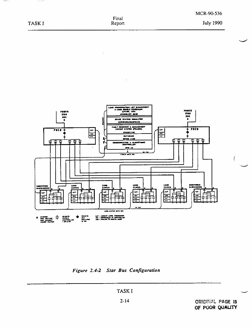
A star-bus configuration (Figure 2.4-2) has been developed to distribute 120 Vdc (formerly
150 Vdc) in a separate MSFC breadboard. In the star-bus configuration, load centers are fed
dire,._ly via RBI's and 3 kW RPC's from the PDCU's. This star-bus configuration is the present
baseline for the +120 Vdc distribution system and has been developed as a working breadboard at
MSFC.
TASKI
2-8

TASK IFinal
Report
MCR-90-536
July 1990
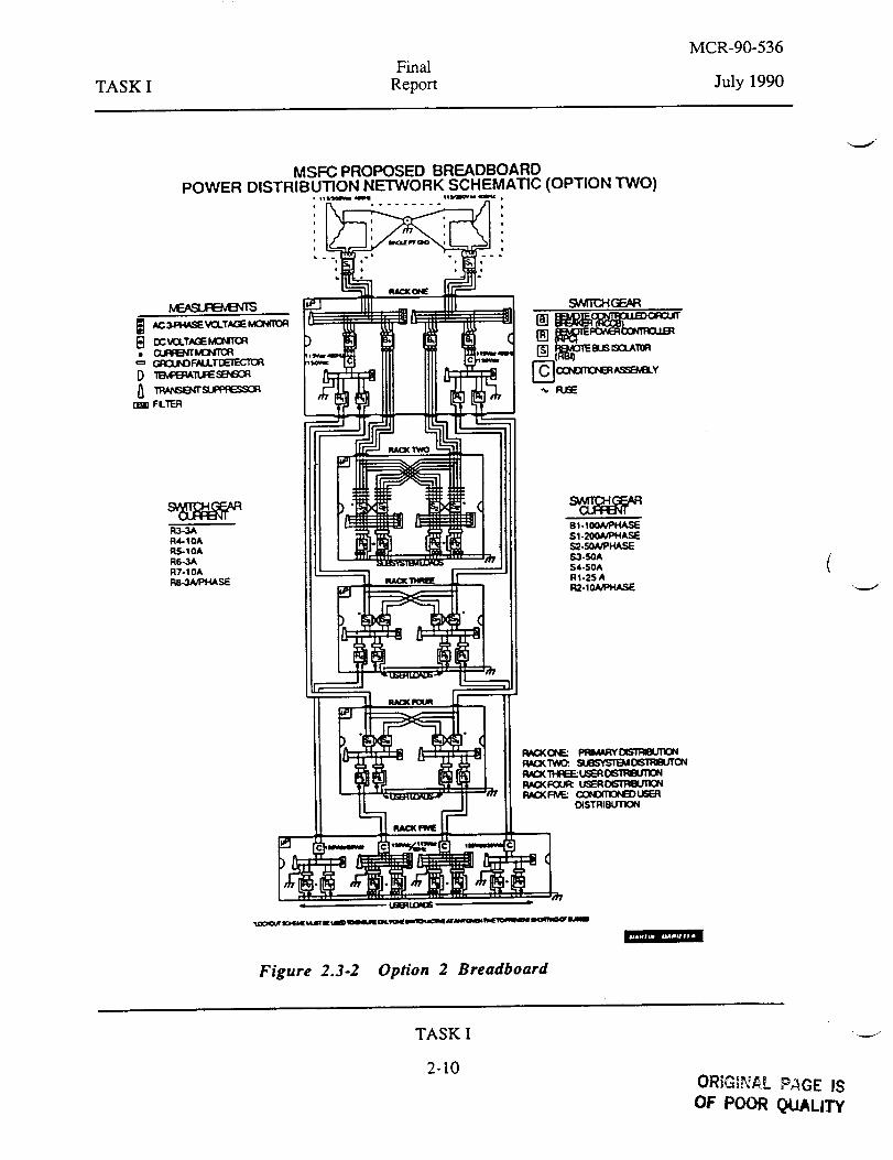
MSFC PROPOSED BREADBOARD
POWER DISTRIBUTION NETWORK SCHEMATIC (OPTION ONE)
AC 34uq.4d_E VOLT_C_ MCIMTO R
_] IX::VC3.T_ MO'dl_R
• CURRB_
== GFIOUND F4d.L.T Db_I_'IT3R
D _IURESB'8:_
A rR_l___ FL'n_
_1 I1_1_ _-_
R$,.tOA
Rr=-,1,_=HASE
R7- IOARIHASE
R_IO_PHASE
R 1 'I-3AR=t._SE
R 12,3A,4IHASE
81- l 0OARI't.t4.SE
St-2CO_=HASE
S2- .r_/VI=_ASE
S3-20A_t=_SE
S4-S0A_HASE
SS-SOA_HASE
R _-2SAR=_3E
R2-2SAR_ASE
R3-2SA_U_E
1_4_K ONE: PI_M_RY 0_r1:mUl"lON_¢=m_ _ I_O( I_Q SI._'VSTI_ 061ReUtON
_ i P_O(R3UR tJ_0_I=_Lr;1C_
_7tll / nKXRV_ CONOmO_tJ_tD_STRI_JTION
w__.L3.._,_ ._2_*,. ._, *._._=............
Figure 2.3-1 Option 1 Breadboard
TASKI
2-9OOl_,_*_ ?'AGE IS
OF POOR Q4.JAHTY
TASKIFinal
Report
MCR-90-536
July 1990
MSFC PROPOSED BREADBOARDPOWER DISTRIBUTION NETWORK SCHEMATIC (OPTION TWO)
R3-3AR4-10ARS-10AR6_3ART-10ARa.3A/PHASE
Bt -100A/PHASE$1-200kI_ASES2-SOA/PHASES.1-50A54.50AR1-25 A
Figure 2.3-2 Option 2 Breadboard
TASKI
2-10
ORiGI._._L P_GE IS
OF POOR QUALITY

TASKI
Final
Report
MCR-90-536
July 1990
MSFC PROPOSED BREADBOARDPOWER DISTRIBUTION NETWORK SCHEMATIC (OPTION THREE)
R2-3AR3-10A
R4-3ARS-10AR6-10AR7-3/VPHASE
BI-t00A"S 1-3SOA
S2.50A/PHASE$3-$0AS4-SOARI-lCl/PHASE
Figure 2.3-3 Option 3 Breadboard
TASKI
2-11

TASKI
Final
Report
MCR-90-536
July 1990
MSFC PROPOSED BREADBOARDPOWER DISTRIBUTION NETWORK SCHEMATIC (OPTION FOUR)
R3-10/VPHASER4-3ARS-10AR6-10AR7-3ARS.3A/PH_ERg-10A
u_tJN _lirr4
Figure 2.3-4 Option 4 Breadboard
TASK I
2-12ORIGINAL PAGE ISOF POOR (_JAL.ITY

TASK I
Final
Report
MCR-90-536
July 1990
PIIIgll[S
BINSOIlS
t ' 1¢ _ I c ¢ _' '] ¢
m
I
I' i .....
i !
:J,l,¢: :: 1 ) Q I
t_-tTTTT_ II-_TTrrl
0 mlm/l_ ..J- 1lion4 I_ n4m054Rig VCLTILI4 "I" POIl|l COU TXOLL |0
m 0_ IOA)W le Iml
::.-.I. I. :::-.I,
LHe cca¢l eala o_
_tuoq4 _. t,.4pmq_r ut'4q_ _ln_mouo K • _ w _IWO_LIIOOUIY0el Lag • dUSd.040 1"0 mlV6l. ¢6n0_l| iV
PII[I
BINS
IIII1
, ,...!=.=./,,,¢' ,,,
Figure 2.4-I Ring Bus Configuration
TASKI
2-13
TASKI
Final
Report
MCR-90-536
July 1990
PIIIII|II
Till
01|
:I'TTTI
J
I, IIIIII IIIlll INllil i
IIISTIIIImlTI| | LII
[,J
Figure 2.4-2 Star Bus Configuration
TASKI
2-14 ORTG!_,i_L PAGE IS
OF POOR OUALITY

TASK H
MCR-90-536
Final
Report July 1990
3.0 TASK
Har_twwe Selection
The types and quantities of deliverable hardware which was selected to be incorporated into
the MSFC breadboard is listed in Table 3.2-1. This list has been compiled and revised throughout
the history of the contract. The original list was developed based on the breadboard topology
selected, the original contract value, and the estimated cost of the individual hardware items. This
original list was revised several times throughout the history of the program through a series of
add-on and change-order proposals.
3.1 T_chnology Readiness Assessment
A technology readiness assessment report was developed during Task 2 which identified
pieces of equipment requir,:.g de velopment effort to support the Space Station phase C/D effort.
Equipment lists were developed from the previously selected network schematics. Additionally,
functional requirements for the network equipment as well as other requirements which affected the
suitability of specific items for use on the Space Station program were identified. A copy of this
technology readiness report can be found in Appendix I.
TASK H
3-1

Table 3.2.1 MSFC Breadboard Hardware (as of July, 1990)
Hardware Assembly Number of Units
Remote Power Controller (RPC)AC 1 kW 20AC 3 kW 12DC 1 kW 35DC 3 kW 15
Remote Controlled Circuit Breaker (RCCB)AC 10 kW 9DC 10 kW 6
Remote Bus Isolator (RBI)AC13(2
Generic Controller Circuit (GC)
Switchgear Interface Controller (SIC)
Analog-to-Digital Card (A/D)
Card Cage
Test Tool
Temperature Sensor
Voltage SensorsDC 120 VAC 208 V, 20 kHz
Current SensorsDC 15 ADC 50 ADC 100A
Transorbs
SIC-LLP Interface Cables
42
80
14
9
5
1
40
4232
121617
15
15
TASK II
3-2

TASK III
MCR-90-536Final
Report July 1990
4.0 TASKIH
Hardware Advanced Development and Verification Tests
This section describes the requirements and design of each individual hardware assembly
developed on the Space Station Common Module Network Topology and Hardware Development
Program. Assembly requirements were derived based on the SSM/PMAD requirements developed
during Task I and on the selec:ed SSM/PMAD network concepts. Basic requirements and
simplified design block diagrams are included in Section 4 for each assembly. Appropriate
appendices have been added to include equipment specifications and product control drawings
where applicable. These appendices are referenced in their proper assembly sections.
4.1 Switchgcar Interface Controller (SIC)
4.1.1 SIC Requirements
The Switchgear Interface Control (SIC) Card is required to communicate with a Lowest
Level Processor (LLP), 14 GeneIic Controller (GC) Cards, and an Analog to Digital (A/D) Card.
The SIC must process 19 different commands sent from an LLP and return response data
consistent with the LLP/SIC in:erface document found in Appendix II. Also, a SIC must
communicate with 14 GC cards, each of which is capable of controlling and monitoring a Remote
Bus Isolator (RBI), a Remote Controlled Circuit Breaker (RCCB), or a Remote Power Controller
(RPC). Additionally, a SIC communicates with an A/D card and receives 16 voltage, current, and
temperature sensor data inputs.
4.1.2 SIC Desima
The SIC is designed to provide and receive command and data information from a lowest
level processor, 14 GC cards, ar'd an A/D card. This information is processed in a 6800 8-bit
microprocessor programmed via a 2764 EPROM. A simplified block diagram of the SIC can be
found in Figure 4.1.2-1.
TASK Ill
4-1

TASK lIIFinal
Report
MCR-90-536
July 1990
I
1.843 MHzl I Interface
Crystal _ Circuitry
Oscillator ! I
Microprocessor Control
Electronic Circuitry
GC Serial Data
RS422 Receive_+
RS422 Recei a-
q_$422 Transmit +
._1:lS422 Transmit -
ND CJock
16 AddressLines
MC6800
Microprocessor
8 Data
Lines
Isolator Receiver Serial-to-
Parallel
Converterand
Line to-Serial
D river Converter
Clock +10 Vdc Unregula,edJ
20 kHz, 208 VnnrtsJ
To A/D Card
L
A/D Card
Decoder-
Driver
Rectilier/Filterl
Unear Regulator
Power Supply
+5 Vdc for SIC
(
Figure 4.1.2-1 Switchgear Interface Controller Card
TASK III
4-2

MCR-90-536
Final
TASK III Report July 1990
A SIC communicates serially with an LLP via optically-isolated RS-422 transmit and receive lines.
The serial data that is received by the SIC is passed to a serial-to-parallel (8-bit) converter and
transferred to the system data bus. Outgoing data from the SIC to LLP is transferred in the reverse
order - flu:st through a parallel to serial converter and then through a line driver to an optically-
isolated receiver on the LLP. Data transfer occurs at the system clock rate of 640 kHz. A copy of
the 19 different LLP to SIC command and response formats may be found in the SIC to LLP
Interface Document in Appendix II.
A SIC also communicates seriall/with up to 14 GC cards. The SIC provides the GC cards with
Data Enable, ON/OFF, and system clock inputs. The GC provides the SIC with serial data
including switch status, fault, and current level information.
Communication between an A/D card and a SIC occurs directly on the system address and data
busses. The SIC also provides the A/D card with system clock and interface read/write control
lines.
The SIC uses a Motorola 6800 8-bit microprocessor to control system I/O, store data, and process
commands. The compiled assembly code is contained on a 2764 EPROM and is found in
assembly drawing #849NWT31126. The assembly code contains over 3000 lines of code and is
compiled by a 2500 A.D. 6800 MacroAssembler. The resulting compiled object code is linked to
create the executable binary file that resides on the EPROM.
4.2 Generic Controller (GC) Card
4.2.1 GCRequirements (Od_nal)
A Generic Control (GC) Card is required to control the switching operation of a 20 kHz or
DC RBI, RCCB, or RPC and return switch status information to the SIC. The GC card receives
command data information from a SIC and "decides" whether or not to command a switch on or
off (according to the Truth Table in 4.2.1-1). Additionally, the GC card processes analog signal
information passed to it from a switch and decides when to "trip" a switch. Conditions which
TASK III
4-3
MCR-90-536Final
TASK III Report July 1990
warrant the GC tripping off a switch are Under Voltage, Over Current (I2t), Surge Current,
GroundFault,andOverTemperatureconditions. Additionally, anOverTemperaturewarning,a
currentlimit switch turnonprocessor,andzero voltage and current crossing detectors are present
on the GC. Values at which each of these conditions occur are listed in Table 4.2.1-2.
SIC to GC INPUTS
ON OF.___.EF SWITCH STATUS
0 0 ON (HARDWARE ERROR)
0 1 ON
' 0 OFF
1 1 NO CHANGE
Table 4.2.1.1 GC Card Truth Table Requirements
Condition Values
Under Voltage
Over Current (I2t)
Surge Current
Ground Fault
Over Temperature Trip
Over Temperature Warning
Current Limit Turn On
85% of Line Voltage
115% RMS Current
400% RMS Current
50 mA for 40 mS
125 Degrees Celsius
100 Degrees Celsius
130% RMS Current
Table 4.2.1-2 GC Card Processor Trip Level Requirements
TASK III
4-4
v

MCR-90-536Final
TASK II/ Report July 1990
4.2.2 GC Desi__ (Original)
The Generic Card (Figure 4.2.2-1) is the controller board for any type of AC or DC switch
(RBI, RCCB, or RPC). Each GC Card is capable of controlling and monitoring one switch, and
can communicate serial switch intormation to one of two possible SIC cards. The GC takes analog
signal processor, switch status, switch configuration, and SIC command information through a
state machine (ALTERA Programmable Logic Element and 2764 EPROM) to control the switching
operation of a switch. The GC provides the SIC card with serial data via an analog-to-digital
converter and a parallel-to-serial converter.
The analog processors which are present on the GC can be found in Table 4.2.2-1. The output of
each of these processors provides inputs to the state machine and describes which, if any, trips
have occurred on the switch. A block diagram schematic of each of the analog processors listed in
Table 4.2.2-1 can be found in Figure 4.2.2-2.
Under Voltage
Zero Voltage Xing
Ground Fault
Table
Over Temp Trip
Over Temp Warning
Zero Current Xing
I2t Trip
Surge Current Trip
Inrush Over Current
4.2.2-1 Analog Signal Processors
The GC receives switch status information from the switches in the form of either or both a
mechanical (relay) and a main (solid-state) status. The GC uses pull-up resistors via the
switchgear to develop the proper digital signal which feeds the state machine (Figure 4.2.2-3).
The GC card state machine operation is dependent upon which type of switch it is controlling.
Figure 4.2.2-4 shows the various configurations for AC and DC RBIs, RCCBs, and RPCs. Each
of the various configure lines influences the path that the state machine takes during its operation.
Table 4.2.2-2 lists each line which determines a switch's configuration and describes what each
TASK III
4-5
TASK ILlFinal
Report
MCR-90-536
July 1990
ANALOG SIGNAL PROCESSORS
- Under Voltage- Zero Voltage Crossing- Ground Fault
- Over Temp Trip- Over Temp Warning- Zero Current Crossing- 12t Trip- Surge Current Trip- Inrush Over Current
SWITCH STATUS
Relay Status (AC Switchgear)- Main Switch Stares
SWITCH CONFIGURATION
- ZE1- ZE2
- SCE1- SCE2- Inhibit- Status Discrete
- Inhibit Surge I- Bypass Trip
SIC COMMANDS
- Clock- Data Enable.-On-Off
CMDICMD2CMD3CMD4
- Data
AL'IERACHIPSTATEMACHINEGENERATOR
POWER SUPPLIES
+5 Vdc Regulated- +15 Vdc Regulated- - 15 Vdc Regulated
SWITCH ON/OFFCONTROLS
w_
INFORMATION
Figure 4.2.2-1 Generic Controller Card
TASK III
4-6

TASK IIIFinal
Report
MCR-90-536
July 1990
AnalogCurrent
sig.al !Buffer/Filter
Comparator
Multiplier
RMSConverter
ZeroCurrent
Crossing
v
Comparator
Integrator/Comparator
Comparator
SurgeCurrent
I2t Trip
Over
Current
Trip
v
v
v
AnalogVoltageSignal
Comparator
Comparator
v
Under Voltage Trip
Zero
Voltage Crossing
Gnd Fault Current
Analog Signal
Buffer+/- DualComparators
Comparator
Gnd Fault Trip
v
TemperatureSensor Analog
Signal Amplifier/Filter
Comparator
TempTrip
Over TempWarning
Figure 4.2.2-2 GC Card Analog Processors
TASK III
4-7

TASK III
MCR-90-536
Final
Report July 1990
SWITCH
RELAY AUX
CONTACTS
OR GND
TRANSISTOR _,_
SWITCH
OR GND
+5 VDC
_i$,
GENERIC CARD
MECHANICAL
SWITCH
STATUS
VDC
$4,
Figure 4.2.2-3 Generic Card Switch Status
SOLID-STATE
SWITCHSTATUS
Circuitry
CONFIGURATION LINE AC RBI AC RCCB AC RPC DC RBIZE1 OM (74 OFF CNZE2 O_ (74 OFF (74SCE1 CN OM CFF Oq
OqOFFCN
SCE2 Oq
OFFCN
INHIBITOFFOFFOFFINHIBW SURGEI
CN
OFFCN
DC RCCB DC RPCQ=F CFFCFF OFFCFF CFF:OFFOFFCN
OFFCFFOFF
INTWlCE CN CN OFF CN CN CNBYPASS TRIP CN OFF OFF CN C_cF OFF
STATUS DSCRT NOT USED NOTUSED NOTUSED NOTUSED NOTUSED NOTUSED
NOTE: 'ON' is GND AND 'OFF' IS +5 VDC
Figure 4.2.2-4 Generic Card Configurations
TASK III
4-8

MCR-90-536
Final
TASK III Report July 1990
one does. Additionally, several of these lines are not currently being utilized and are identified as
such.
Configuration Line Description
ZE1
ZE2
SCE1
SCE2
Inhibit
Not Used
Not Used
Smart Contactor Enable (Not Used)
Smart Contactor Enable (Not Used)
When 'ON', the switch is inhibited
Normally tied to +5, but can be
used with 'status discrete' for
cross-strapping purposes
Inhibit Surge I When 'ON', the switch will not trip
on a surge current trip
Intwice When 'ON', the switch will not get
a 'second chance' to turn back on
when a current trip occurs
Bypass Trip When 'ON', the switch will not trip
off on any form of trip (over
current, under voltage, over temp,
gnd fault, etc.). Used only on an
AC or DC RBI.
Stares Discrete
Table 4.2.2-2 - Switch Configuration
Used in conjunction with Inhibit -
used when switches are cross-
strapped (a failure of one switch
causes another to turn on)
Lines and Descriptions
TASK III
4-9

MCR-90-536Final
TASK III Report July 1990
The GC Card state machine utilizes 13 separate states to control the switching operation of a
switch. This state machine resides internal to the ALTERA chip. The various states are decoded
and switches are turned on and off via a 2764 EPROM.
Upon any given power up or if an off command or inhibit is received, the ALTERA chip enters
state 0 and all switches get commanded off. The remaining state machine sequencing is described
in Figure 4.2.2-5.
4.2.3 GC Requirements ( DC only GC)
Following the decision to develop a +120 Vdc breadboard in January, 1989, a generic
controller card was designed and de ,oped which was required to control only DC switchgear.
The functional requirements of the new DC-GC are identical to those of the original GC with the
exception that the new GC is required to control only DC switchgear.
4.2.4 GC Design (DC only GC)
The DC-only Generic Card (Figure 4.2.4-1) is the controller board for any type of DC
switch (RBI, RCCB, or RPC). Each DC-GC Card is capable of controlling and monitoring one
switch, and can communicate serial switch information to one of two possible SIC cards. The GC
takes analog signal processor, switch status, switch configuration, and SIC command information
through a state machine (ALTERA Programmable Logic Element) to control the switching
operation of a switch. The GC provides the SIC card with serial data via an analog-to-digital
convener and a parallel-to-serial convener.
The analog processors which are present on the DC-GC can be found in Table 4.2.4-1. The
output of each of these processors provides inputs to the state machine and describes which, if
any, trips have occurred on the switch. A block diagram schematic of each of the analog
processors listed in Table 4.2.4-1 can be found in Figure 4.2.4-2.
TASK III
4-10

TASK 11IFinal
Report
MCR-90-536
July 1990
IITAI'I II
_IHI IUE_y. WAft mimicOLI,,LS'_'r T_[_n A,U aW_
_ Ilii_yll19
AND I_lml'l'_l II_l
I,_L, Ilwrl_llll _ul (11_
I IITATTI 4
_ON_I IUB_I'. Wait
_ A,tE Ot_
ItTA '1_ $
OCL"UtBM) _UO_ NO_
|TA 1"11?
A/,,L.Jlwrl_#_ _Ai[ k_l_ CW
_ID.A Y. CLIIAIB_ IJI4T. 4._0_rTA'r I_pJI UiV_.,_
'nUP O_D,R:.
A_ D'r, A P.q_l C_Ut ll_ff. OI A _
ITAT| U j
rrAi1E 6
lUlX ol_M _ swl_w_uT D i4[_,sE_&
IUO_¥ a_l IrflU. _
w_rl" m k_LJL,B_I_iCUIUUDffUB4TIWlrlT_ _
ITATI li
"/TJ_4ore I,¢41v,t._(UIUIiI_T
|TAT| U
'1_1_01_ BJLAY Wa_f'_
,klUl NDlr_q_
IrT,l_TII •
_'11I Ih4AIl,IsquP_'I[]I_ AI'A"_
JmI,Y IIUI UPVIIL Ap*I(_plu
A_O_"IJIJL
i,
I_TAT'I U
IITA Y Ikl_ll le./-m Uml_A_ CPF _"J_*4D 8 Dm,U_
Figure 4.2.2-5 GC Card State Machine
TASK 1II
4-11OE POOI_ QUALITY

TASK IIIFinal
Report
MCR-90-536
July 1990
Under Voltage
Over Temp Warning
Over Temp Trip
Surge Current Trip
Inrush Over Current
I2t Trip
Ground Fault*
* Present on the DC GC but not implemented on the DC RPCs
Table 4.2.4-1 DC-GC Analog Signal Processors
The DC-GC receives switch status information from the switches in the form of a switch type
signature (lkW RPC, 3 kW RPC, or RBI) and a main (solid-state) switch status. The DC-GC
uses pull-up resistors via the switchgear to develop the proper digital signal which feeds the state
ine (Figure 4.2.4-3).
ANALOG SIGNAL PROCESSORS1
- Under Voltage /- Ground Fault I
- Over Temp Trip ' [Over Temp WarningI2t Trip ALTERA
- Surge Current Trip CHIPInrush Over Current STATE
MACHINEGENERATOR
SWITCH STATUS
- Switch Type (I or 3 kW)- Main Switch Status
v
SIC COMMANDS t
SWITCH ON/OFFCONTROLS
v
INFORMATION
POWER SUPPLIES
+5 Vdc Regulated+ 15 Vdc Regulated- 15 Vdc Regulated
k...4.-
Figure 4.2.4-1 DC.Generic Controller Card
TASK III
4-12

TASK IIIFinal
Report
MCR-90-536
July 1990
AnalogCurrentSignal
I Buffer/Filter Multiplier
RMSConverter
Comparator
Integrator/Comparator
Comparator
SurgeCurrent
I2tTrip
Over
Current
Trip
v
v
v
AnalogVoltageSignal
_[ Comparatorv
Under Voltage Trip
Gnd Fault Current
Analog Signal*
Buffer+/- Dual
Comparators
Comparator
Comparator
Gnd Fault Trip
TemperatureSensor AnalogSignal
Amplifier/Filter
* Signal Not Provided by Existing DC RPCs
TempTrip
v-
Over TempWarning
Figure 4.2.4-2 GC Card Analog Processors
TASK III
4-13

MCR-90-536Final
TASK II-I Report July 1990
SWITCH +5 VDC
/Open or Closed II(lkW or 3kW) F
TRANSISTOR
SWITCHOR GND
$4,
+5 VDC
GENERIC CARD
1 or 3 kWDC RPC
Signature
SOLID-STATESWITCHSTATUS
Figure 4.2.4-3 Generic Card Switch Status Circuitry
TASK Irl
4-14

MCR-90-536
Final
TASK IIl Report July 1990
The DC-GC Card state machine utilizes 6 separate states to control the switching operation of a
switch. This state machine resides internal to' the ALTERA chip.
Upon any given power up or if an off command or inhibit is received, the ALTERA chip enters
state 0 and all switches get commanded off. The remaining state machine sequencing is described
in Figure 4.2.4-4.
4.3 Analog to Digital (A/D) Card
4.3.1 A/D Requirements
The Analog to Digital (A/D) Card is required to accept 16 voltage, current, and temperature
sensor inputs and return proportional digitized information to the SIC card. The A/D card
processes the analog sensor inputs and returns digitized RMS voltage, RMS current, average
voltage, average current, frequency, average power, instantaneous power, power factor, and
temperature data to the SIC card. The required sensor input levels to the A/D and their 8-bit
equivalent which gets passed to the SIC can be found in Table 4.3.1-1.
Digital Input Range
Inputs Used Processors Analog Input Range (Base 10)
Voltage (V) RlVlS, Ave., Freq. -10V to 10V 0 to 255
Current (I) RMS, Ave. -10V to 10V 0 to 255
V & I Inst. Pwr, Ave Pwr., Pwr Factor -10V to 10V 0 to 255
Temperature Temperature 2342 to 8806 Ohms 0 to 255
Table 4.3.1-1 - Required AID Card Sensor Inputs, Processors and Ranges
TASK III
4-15

TASK 117Final
Report
MCR-90-536
July 1990
¢.,,.I
t'-¢:
It.It.Oe"
O'J0')
i
09
v
Enter State 0at Power Up
STATE 0 - NULL STATE |Turn Main Switch OFF
Time: 50 mS
STATE 1Pulse Off Coil
Time: 50 mS
STATE 2-OFF
OFF
I SIC Issuesan ON Command
STATE 3 - Pulse On Coil
Time: 50 mS
..Q
.I
r-e.-
IiU..
Ot-
o_
e9o'J
I
_cA09
,LSTATE 4 - ON
Main Switch is Turned
On
_1t' No Trip
Trip(UV, Temp, 12T,
Surge, Fast) ,._[ISTATE 5 - Trip StateMain Switch is Turned
"1o.
Figure 4.2.4.4 DC-GC Card State Machine
TASK III
4-16

MCR-90-536Final
TASK III Report July 1990
4.3.2 A/D Design
The analog to digital card accepts voltage, current, and temperature analog inputs and
returns eight-bit digital information to the SIC. A functional block diagram of the A/D card is
shown in Figure 4.3.2-1.
Current and voltage sensor inputs are accepted and passed through MC34004 difference
amplifiers to allow for proper signal referencing and isolation. The (16) voltage and (16) current
sensor signals are then passed through an analog multiplexer. The proper channel is selected via
the SIC address bus when the SIC requests data from a given sensor. Several analog processors
reside on the output of the multiplexers including amplifier/integrators, RMS converters, and an
analog multiplier. These chips process the appropriate analog signal which allows average, RMS,
and power readings to be available to the A/D converter. Following these analog processors is
another multiplexer stage which allows the SIC to select what type of reading it desires from the
A/D card (voltage, current, temperature, average, RMS, etc.). The proper channel is selected via
the SIC address bus as with the previous multiplexer.
Temperature sensor inputs are accepted and fed into the inverting input of a single-ended
MC34004 operational amplifier. Any variation in the impedance of the temperature sensor results
TASK III
4-17

MCR-90-536Final
TASK III Report July 1990
in a change in the output voltage of the operational amplifier. This amplifier inputs to the second
stage multiplexer as described above.
The selected output of the second multiplexer is input to an SI8601 analog-to-digital
converter which is referenced at 5 VDC. The gain of each amplifier stage feeding the A/D
converter is set to input 2.5 VDC at 100% sensor rating (5 V analog at the input to the A/D card).
This allows the A/D card to have a +/- 200% sensor rating range.
TASK III
4-18
v _

TASK m
Final
Report
MCR-90-536
July 1990
iiiiiiiiI
000 000
4
>1 I>
• _
_ __" - ,,
- [
A
_oo
Figure 4.3.2-1 Analog to Digital Card
TASK III
4-19 ORfG_t_L PAGE tS
OF POOR QUALITY

TASK IIIFinal
Report
MCR-90-536
July 1990
4.4 AC Remote Power Contrcller (RPC)
4.4.1 AC RPC Requirements
An AC Remote Power Controller 0RPC) is required to provide 5A (lkW) or 15A (3kW) at
208 Vrms, 20kHz to any resistive, capacitive, or inductive load. The switch is SPST with a main
solid state switch, a parallel current limiting switch, and a relay isolator. Commanding on and off
of the RPC is controlled by a GC card.
The RPC provides the GC with analog current, voltage, ground fault, and temperature
sensor inputs. A ditional switch telemetry data which is passed to the GC includes an auxiliary
relay contact and a solid-state switch status indicator.
A "Fast Trip" shutdown circuit is required to be present on the RPC power stage. If a
400% peak current is detected by the RPC, the main solid state switch immediately shuts off
(<luS) and the RPC _urrent limits the fault. Control of the RPC is returned to the GC card for
further processing once the main solid state switch has turned off.
4.4.2 AC RPC Design
The AC RPC (Figure 4.4.2-1) is designed to be a self-protecting SPST switch controlled
from a GC card. The main parts that comprise the RPC are the switching unit, the "fast trip"
circuitry, the analog sensors, and various power supplies.
The switching unit (developed by Leach Corp.) is comprised of a magnetically latching
relay, a main solid state switch, and a parallel current limiting switch; all controlled from the GC
card. The latching relay provides both power and return isolation to the load when the RPC is off.
The relay has a +24 Vdc coil and is magnetically latching with an auxiliary contact which provides
relay status information to the GC card. The main solid state switch is comprised of parallel
MOSFETS and is in series with the main relay contracts. Parallel MOSFETS are required to
TASK IH
4-20

TASK IIIFinal
Report
MCR-90-536
July 1990
_,z., I
E
7"2
Figure 4.4.2-1
t- t-
I '_ * l._v/ L J::E=
N
o . . o ....... o o .
<
.td , ; I
0_
AC Remote Power Controller
i°ii
I
|
!
f
!
E.IL_L_
Z--<"_ _ L)
TASK III
4-21

MCR-90-536Final
TASK III Report July 1990
provide sufficient carrying capability and to reduce the MOSFET on resistance. This prevents
large voltage drops from appearing across the RPC (<3 Vrrns). The main solid state switch
provides zero voltage turn on and zero current turn off switching for the RPC.
In parallel with the main solid state switch is a solid state current limiting switch. The
current limiting switch is comprised of parallel MOSFET switches in series with an inductor. The
inductor provides sufficient impedance at 20 kHz to limit any inrush or fault current to 130%
RMS. The main and current limiting solid state switches both have optically isolated gate drives
which significantly reduce cross-talk noise. The GC card controls the main and current limiting
switches such that they are never both on at the same time.
The "fast trip" circuitry detects peak currents exceeding 400% using zener diode sensing
and fast transistor control. Any peak current exceeding 400% rated (positive or negative peak)
cause the main solid state switch to immediately turn off (<1 uS), immediately causing the RPC to
enter the current limiting mode. Additionally, the "fast trip" circuitry returns the status of the main
switch. This fast trip circuitry provides inherent self-protection for the RPC.
The RPC provides the GC card processors with analog data as listed in Table 4.4.2-1. The
GC card, after processing the analog signals, decides when a trip condition has occurred. The
only trip condition which occurs directly on the RPC is the fast trip.
A number of separate power supply voltages and grounds are present on the RPC, as
summarized in Table 4.4.2-2. The latching relay uses +24 Vdc developed on the secondary of a
transformer at the input of the RPC to drive its coil. The secondary of the transformer is rectified
and filtered; using a sufficiently 1 trge capacitor for energy storage in the event of a 20 kHz power
line failure. Control of the relay is done by the GC card. The +12 Vdc current limiting switch
housekeeping power is developed on the same transformer that the relay coil power is developed,
using a separate ground reference. The +12 Vdc is developed via a rectifier-filter-linear regulator
approach.
The +12 Vdc main solid state switch housekeeping power is developed on a second transformer
that is "downstream" from the relay. This insures that housekeeping power is developed for the
TASK 11I
4-22

MCR-90-536Final
TASK III Report July 1990
main solid stateswitchonly after therelay hasbeenclosed. A rectifier-filter-linear regulatoris
usedto developthe+12Vdc. Separate+5, +15,and-15Vdcpower is deliveredfrom theGCcard
to powerthefasttrip circuitry.
Analog Signal RPC Signal Level GC Signal Level
Ground Fault 50 mA 0.50 Vrms
Under Voltage 85 % of 208 Vrms 9.0 Vrms
Current 100% Rated Current 1.0 Vrms
Temperature 100 C -3.73 Vrms
Temperature 125 C -3.98 Vrms
Table 4.4.2.1 RPC Analog Data Given to the GC Card
Voltage Reference Source Load
+5 GC GND
+15 GC GND
-15 GC GND
+24 GC GND
+12 Main Switch GND
+12 CL Switch GND
GC Linear Regulator
GC Linear Regulator
GC Linear Regulator
RPC Rectifier/Filter
RPC Linear Regulator
RPC Linear Regulator
Fast Trip Circuitry
Fast Trip Circuitry
Fast Trip Circuitry
Relay Coil
Main Switch Hkpg
CL Switch Hkpg
Table 4.4.2.2 RPC Housekeeping Power Supplies and Loads
Martin Marietta has developed a preliminary equipment specification guide for a 20 kHz AC
RPC (Appendix IN). This unreleased document is an example of what format a formal equipment
specification would undertake for a flight-type RPC. Included in this document are the controller
card requirements which would reside as part of the RPC. This document was used as a guide in
developing our 20 kHz breadboard RPCs but does not reflect our specific breadboard design.
TASK III
4-23

TASK Ill
MCR-90-536Final
Report July 1990
4.5 AC Remote Controlled Circuit Breaker (RCCB)
-..._j
4.5.1 AC RCCB Requirements
An AC Remote Controlled Circuit Breaker is required to provide 50A (10 kW) at 208
Vrms, 20 kHz to up to 3 fully-loaded 3 kW RPCs. The switch is SPST and consists of a large
relay which switches both the positive and return sides of the 20 kHz. The RCCB may be
switched 'hot'.
The RCCB must provide the GC with analog current sensor data and relay status
information. Commanding on and off of the RCCB is controlled by a GC card.
4.5.2 AC RCCB Design
The AC RCCB (Figure 4.5.2-1) is designed to provide 20 kHz power for up to 3 fully-
loaded 3 kW RPCs. The main parts that comprise the RCCB are the relay, the relay interface
electronics, and the current transformer.
The relay is used as a single pole, double throw magnetically latching relay with 2 power
contacts and an auxiliary contact used for relay status information. The relay is manufactured by
Leach Corp., and has a current rating of 120 amps.
The relay interface electronics included protection diodes across the relay coils, an inductive
kickback prevention diode for the +15 VDC supply from the GC Card, and an energy storage
capacitor to insure rapid turn on and turn off of the relay.
The current transformer is designed to provide the GC Card with an analog voltage signal
proportional to the AC RCCB current. An RCCB current exceeding 115% of rated (10 kW at 208
Vrms) will result in the GC Card 'tripping off' the AC RCCB.
TASK III
4-24

TASK IIIFinal
Report
MCR-90-536
July 1990
208V ,20 kHz,
I
|
ONII TO GC CARD
[OFF _ ,
! I
I |
II I)
I II
! .
_TO LOAD
|
' TO LOAD
JSTATUS CONTACT
TO GCCARD
Figure 4.5.2-1 AC Remote Controlled Circuit Breaker
4.6 AC Remote BUS Isolator (RBI)
4.6.1 ACRBIR 'firements
An AC Remote Bus Isolator is required to provide 15 kW, 208 Vrms at 20 kHz to RCCB
switches. The switch is SPST and consists of a large relay which switches both the positive and
return sides of the 20 kHz. The RBI can only be switched when the 20 kHz power is off.
The RBI must provide the GC card with relay status information only. Commanding the
RBI on and off is controlled by a GC card.
4.6.2 ACRBIDesign
The AC RBI (Figure 4.112.2-1) is designed to provide 20 kHz power to an AC RCCB.
The main parts that comprise the RBI are the relay and the relay interface electronics.
The relay is used as a single pole, double throw magnetically latching relay with 2 power
contacts and an auxiliary contact used for relay status information. The relay is manufactured by
Leach Corp., and has a current rating of 120 amps.
TASK 117
4-25

MCR-90-536Final
TASK III Report July 1990
The relay interface electronics included protection diodes across the relay coils, an inductive
kickback prevention diode for the +15 VDC supply from the GC Card, and an energy storage
capacitor to insure rapid turn on and turn off of the relay.
4.7 AC Voltage Sensor
4.7.1 AC Voltage Sensor Reqoirements
An AC voltage sensor is required to provide a differential isolated voltage input to one of
16 voltage channels present on an A/D card. The secondary voltage is required to be 5.00 +/- 0.25
Vrms for a prim input of 208 Vrms, 20 kHz.
4.7.2 AC Voltage Sensor Design
The AC voltage sensor (Fi=._e 4.7.2-1) is comprised of a primary DC blocking capacitor,
a step-down transformer, and ar_propriate burden resistors to provi _ - 5 Vrms out for 208 Vrms in.
A 0.01 uF, 600V capacitor is in series with the transformer primary winding to prevent any
DC bias from appearing across the winding. A net resulting volt-second imbalance from the dc
bias across the transformer could result in the transformer saturating, resulting in the failure of the
sensor.
The transformer used in the sensor is a Corona Magnetics 1383B. The primary winding
has 650 turns and the secondary winding has 46 turns.
Appropriate secondary voltage divider resistors are chosen such that the output voltage is 5
Vrms for an input of 208 Vrms.
TASK II/
4-26

TASK IIIFinal
Report
MCR-90-536
July 1990
208 Vrms
0
S.I.T.
0.01uF
-[6,°I 46Turns Turns
1000
0
5 Vrms
0
Figure 4.7.2-1 AC Voltage Sensor
4.8 AC Current Sensors
4.8.1 AC Current Sensor Requirements
An AC Current Sensor i,: required to provide a differential voltage input to one of 16
current sensor channels present on an A/D card. The output voltage of the current sensor for
various current sensor values is listed in Table 4.8.1-1.
Frequency Current Sensor Value Inpu_ Rcqd Output Voltage Level
20 kHz 50 mA Ground Fault
20 kHz 15A
20 kHz 50A
20 kHz 100A
20 kHz 125A
5.00 +/- 0.25 Vrms
5.00 +/- 0.25 Vrms
5.00 +/- 0.25 Vrms
5.00 +/- 0.25 Vrms
5.00 +/- 0.25 Vrms
Table 4.8.1-1 - AC Current Sensor Requirements
TASK 117
4-27

MCR-90-536Final
TASK III Report July 1990
4.8.2 AC Current Sensor Desi__
The 15, 50, 100, and 125 AC Current sensors (Figure 4.8.2-1) are comprised of a 1:200
turn transformer with appropriate burden resistors to provide a 5 Vrms output at rated current.
Rated Curf-ent
o
200
Turns
o
Rburden
O
5 Vrms
Figure 4.8.2-1 AC Current Sensor
The 50 mA differential AC Current sensor (Figure 4.8.2-2) is comprised of a 15 turn
source and return primary winding and a 200 turn secondary winding. The sensor is designed to
handle up to 10 kW at 208 Vrms, 20 kHz and to output 5 Vrms at 50 mA differential current
between the source and return windings.
Source o
Return o [ I
Turns
0
[R burden
O
5 Vrms
0
Figure 4.8.2-2 50 mA Current Sensor
TASK III
4-28
MCR-90-536Final
TASK III Report July 1990
4.9 Temperature Sensors
4.9.1 Temperature Sensor Requirements
A temperature sensor is required to provide a variable resistance input to one of the 16
temperature channel inputs on an A/D card. The output resistance of the temperature sensor for
minimum and maximum temperatures is listed in Table 4.9.1-1.
Temperature (Celsius) Temp. Sensor Resistance (Ohms)
-30 8806 +/- 500
+85 2342 +/- 500
v
Table 4.9.1.1 Temperature Sensor Requirements
4.9.2 Temperature Sensor Design
The temperature sensors selected for use in the ACM/PMAD breadboard are LTN-11C
(Linear Thermistor Network) sensors. The impedance of the output of the sensors is inversely
temperature dependent. The sensors satisfy the requirements as listed in Table 4.9.1-1.
TASK III
4-29

TASK IIIFinal
Report
MCR-90-536
July 1990
4.10 DC Remote Power CQntroller (RPC)
4.10.1 D(7 RPC Requirements
The DC Remote Power Controller is a single-pole, single-throw switch required to provide
8.33A (1 kW) or 25.0 A (3 kW) at 120 VDC to any resistive, capacitive, or inductive load. The
switch is required to operate either above or below a load with the switching occurring via a solid
state switch. Commanding on and off of the RPC is controlled by a GC Card.
The RPC provides the GC with analog current and temperature sensor data. Additional
data which is passed to the GC includes a switch status indicator and an under voltage trip bit.
A current limiter control circuit is present on the DC RPC. The current limiter limits the
current during a fault condition to 400% RMS during the first one microsecond of an event. The
RPC will go into a current limit operation within one microsecond and limit the current to 175%
RMS for a time constant which is dependent upon the voltage across the switch at the time. A dead
short will result in the RPC turning off in approximately 15 mS.
4.10.2 DC RPC Design
The DC RPC (Figure 4.10.2-1) is designed to be a self-protecting, SPST switch controlled
from a GC card. The main parts that comprise the RPC are the switch power electronics and the
switch control circuitry.
The power handling components of the DC RPC include the current measuring shunt, the
current limiting inductor, the MOSFET switches, and the current sense resistors.
Current enters the RPC via the shunt which provides analog current information to an
isolation amplifier and subsequently to the GC card. This input is the input to the I2t processor
which resides on the GC card. A 1 I.tH inductor is in series with the main power path to limit di/dt
V _
TASK m
4-30

TASK HIFinal
Report
MCR-90-536
July 1990
O
O
IRETURN
4,
IsH F-V_/I -
ISOLATIONII TOGC
i
C__G
INDUCTOR,_,
UNDER VOLTAGE
TEMPERATURE
TEMPERATURE I (TO GC CARD)SENSOR
]
GC CARD I
RSENSE
_ CONTROLCIRCUITRY
MOSFETVOLTAGE
Figure 4.10.2-1 DC Remote Power Controller (RPC)
PWR TO LOAD
O
SWITCH
STATUS
croGC)
during a surge event prior to the current limiting control loop responding. Six MOSFET stages for
the 1 kW DC RPC and 18 MOSFET stages for the 3 kW DC RPC are paralleled to handle the
power and reduce the voltage drop across the switch. The sense resistors provide feedback to the
switch control circuitry which provides overload protection to the RPC.
The switch control circuitry takes the GC card ON/OFF command line, the MOSFET
current, and the MOSFET voltage and decides how to operate the switch. Any time an OFF
command is issued from the GC card, the RPC is off. The only time the switch can be on is if the
GC card has issued an ON command.
During non-overload conditions, the MOSFETS are saturated if an ON command has been
issued. Any current fault which exceeds 175% rated value will cause the RPC to go into a current-
TASK III
4-31
MCR-90-536Final
TASK III Report July 1990
sourcemodeof operation (the MOSFETs run linear). The voltage across the switch is sensed and
integrated and compared to a reference signal. If a dead short exists on the output of the RPC for >
15 mS, the RPC will latch off. If the short is removed prior to 15 mS (in the case of charging a
capacitor bank), the switch will turn back on and the MOSFETs will re-saturate.
Additionally, the DC RPC provides an under voltage signal to the GC card which allows it
to trip off the RPC if the line voltage falls below 60 VDC. The RPC is capable of operating either
in the positive or negative leg of the load. The DC RPC as presently implemented in the MSFC
breadboard does not contain ground fault detectors due to the nature of the grounding configuration
which was implemented in the system. The RPCs would need to be designed to wwitch both the
positive and the return sides of the power in order to incorporate ground fault detection.
4.11 DC Remote Controlled Circuit Breaker (RCCB)
4.11.1 DC RCCB Requirements
A DC Remote Controlled Circuit Breaker is required to provide 83.3 A (10 kW) at 120
VDC to up to 3 fully-loaded 3 kW DC RPCs. The switch is SPST and consists of several parallel
power MOSFETS which switch the positive side of the +120 Vdc. The RCCB may be switched
"hot".
The RCCB is required to trip off on any current exceeding 300% for 150 mS. The RCCB
will also trip off on any current exceeding 110% for 5 seconds. The RCCB returns switch status
information to the GC card, as well as an analog current level signal.
The DC RCCB is required to dissipate <1% of power rating at full load, and have a voltage
drop of <1.5 VDC. The DC RCCB is controlled and commanded on and off from a GC card.
4.11.2 DC RCCB Design
The DC RCCB (Figure 4.11.2-1) is a single-pole, single-throw solid-state switch
comprised of a power stage unit developed by Teledyne Electronics and an interface electronics
TASK II/
4-32

MCR-90-536
Final
TASK III Report July 1990
unit. A copy of the Product Control Drawing (PCD) for the Teledyne power stage unit can be
found in Appendix IV (Note: This unit is called an RPC in Appendix IV and is not to be confused
with the Martin Marietta RPC).
++150
Vdc ..
__ AMPLIFIER
SwitchControl/Trip/TelemetryCircuitry
Analog Current Signaland RTN to GC Card
+150 Vdc to Load
Switch ON/Switch Off (From GC Card)
Under Voltage Disable(To GC Card Circuitry)
Switch Status(To GC Card)
+150 Vdc RTN to Load
II,
T
Figure 4.11.2-1 DC Remote Controlled Circuit Breaker (RCCB)
The power stage is comprised of a number of MOSFET switches in parallel capable of
switching 120 VDC, 83.3A. The power stage has a built-in over current curve and is capable of
tripping off during over current conditions. Additionally, the power stage has an under voltage
lockout circuit which will turn the switch off if the line voltage falls below approximately 60 VDC.
The RCCB needs to be commanded off and then on in order to reset the switch.
The interface electronics provide necessary switch status information and current telemetry
information to the GC card. The current level feedback is from a 200 A shunt and amplifier. If the
TASK III
4-33

MCR-90-536Final
TASK Ill Report July 1990
current exceeds 110% of nominal, the GC card will issue an off command to the RCCB via an I2t
trip condition.
4.12 D(_ Remote Bus Isolator (RBI)
4.12.I DC RBI Requirement_
A DC Remote Bus Isolator is required to provide 15 kW, 120 VDC to RCCB switches.
The switch is SPST and consists of a large relay which switches both the positive and return sides
of the DC power. The RBI n only be switched when the DC power is off.
The RBI provides the GC card with relay status information only. Commanding the RBI
on and off is controlled by a GC card.
4.12.2 DC RBI Design
The DC RBI (Figure 4.12.2-1) is designed to provide DC power to a DC RCCB.
main parts that comprise the RBI are the relay and the relay interface electronics.
The
The relay is used as a single pole, double throw magnetically latching relay with 2 power
contacts and an auxiliary contact used for relay status information. The relay is manufactured by
Leach Corp., and has a current rating of 120 amps. The RBI cannot be switched hot.
The relay interface electronics included protection diodes across the relay coils, an inductive
kickback prevention diode for the +15 VDC supply from the GC Card, and an energy storage
capacitor to insure rapid turn on and turn off of the relay.
4.13 DC Voltage Sensor
TASK 111
4-34

MCR-90-536
Final
TASK III Report July 1990
4.13.1 DC Voltage Sensor Reqoi
A DC voltage sensor is required to provide a differential isolated voltage input to one of 16
voltage channels present on an A/D card. The secondary voltage is required to be 5.00 +/- 0.25
Vrms for a primary input of 120 VDC.
ON .......
+t
|
Power In ,I
i i
!
OFF,RELAY
/ TOLOAD
TOLOADw
I t STATUS CONTACTTO GC CARDI
Figure 4.12.2-1 BusAC/DC Remote Isolator (RBI)
4.13.2 DC Voltage Sensor Design
The DC voltage sensor (Figure 4.13.2-1) is comprised of a resistor-divider network which
inputs to an AD 289J isolation amplifier. The resistor-divider provides a sufficient attenuation of
the 120 VDC allowing for an analog signal to be input to the isolation amplifier. A zero-offset and
an adjustable gain potentiometer are present which allows the output of the isolation amplifier to be
set at 0 VDC for 0 VDC input and at 5 VDC for 120 VDC input.
o. < ÷tslT Rr_<
- [ Signal Output
r_.._ Input AD 289J
/o
120 VDC+
SensorOutput
Figure 4.13.2.1 De Voltage $¢Rlor
TASK III
4-35

MCR-90-536
Final
TASK III Report July 1990
4.14 DCCurrent Sensors
4.14.1 DC Current Sensor Requirements
A DC Current Sensor is required to provide a differential voltage input to one of 16 current
sensor channels present on an A/D card. The output voltage of the current sensor for various
current sensor values is listed in Table 4.14.1-1.
Frequency Current Sensor Value Input
DC 15A
DC 50A
DC 100A
Reqd Output Voltage Level
5.00 +/- 0.25 VDC
5.00 +/- 0.25 VDC
5.00 +/- 0.25 VDC
Table 4.14.1.1 DC Current Sensor Requirements
4.14.2 DC Current Sensor Design
The DC current sensor (Figure 4.14.2-1) is comprised of a current shunt which inputs an
analog signal to an AD 289J isolation amplifier. A zero-offset and an adjustable gain potentiometer
are present which allows the output of the isolation amplifier to be set at 0 VDC for 0 amps input
and at 5 VDC for rated current input. An external 15 VDC supply is required to power the
isolation amplifier.
0 DC Cm'_n?
Shunt
O _.d_" Figure
'TTRTNH ,o !sonLInput AD 289J
Isolation Amplifier
4.14.2-1 DC Current Sensor
v
TASK III
4-36

MCR-90-536Final
TASK III Report July 1990
4.15 Card Cage
A card cage is required to provide slot mounting and interface connectors for SIC, A/D,
and GC cards. Each card cage is required to contain (2) sets of the hardware listed in Table 4.15-
1. A detailed design drawing and description of the card cage can be found in Figure 4.15-1.
(2) SICs with LLP Cabling Interface
(1) A/D Card with Voltage, Current, and Temperature Sensor Connector Interfaces
(9) GC Circuits with Switch Connector Interfaces
Table 4.15.1 Card Cage Hardware Requirements
4.16 Test Tool
A test tool is required to provide easy access debugging capabilities for SIC, A/D, and GC
cards. The test tool can simulate an RBI, RCCB, or RPC switch and corresponding switch status,
fault, and command information. External control of the test tool can be accomplished using an
LLP and manual mode software.
TASK III
4-37

TASK mFinal
Report
MCR-90-536
July 1990
14"3
1411
Jl J? JlO JI3 J16 dl? Jr9 d21 JIP_I J2 at J|7
11tJ$O JS? JIS Jt3 Jill J4t J47 .146
J_lil J4¢) J_T d,)l
1ti1J4`1
I '*"'' I I ""J" I I ""'-* I
I""" I I''''J'' Jl `1,---, JI'+"'- J i-,,,,- I[ =,,,,,-,, I
37 PIN ,_l ]
I ='" = I
I "" "= I
L " " " I
I "" "' I
10Pff4
115 PN ,I,111
tS PIN ,/41
i IkO PIN J4
io Pl_ A
tSPIN .141 ]
18 _ Jll ]
I d_QLT
0C F(_lq
8UMq.Y •,.-,] [Irs,'_'v
.18 VOlT
m'lqTAIq
Figure 4.15-1 Card Cage
TASKIn
4-38ORIGINAL _AGE '1-_OF POOR QUALITY

TASK IVFinal
Report
MCR-90-536
July 1990
5.0 TASK IV
(_ommon Module Power Management and Distribotion Breadboard Testing
5.1 Switchgear Interface Controller (SIC)
The SIC cards have been integrated into the SSM/PMAD breadboard and have been tested
with both the 20 kHz and the DC systems. The original design was modified to include optically
isolated transmit and receive lines between the LLP and SIC to prevent the propagation of noise
between the SIC and its LLP. One failure did occur during May of 1990 on a number of SIC cards
when +120 VDC was inadvertently placed on the SIC card return (card cage signal return). The
failure which occurred on the SIC cards would have been prevented if the opto-isolator boards
would have been installed in the Lowest-Level Processors. This event resulted in the failure of a
number of chips on the SIC including the line driver/receiver chip and a number of the RAM chips.
The opto-isolator boards have since been installed in all of the LLPs to prevent the repeat of such
an event. The LLP to SIC interface document (Appendix II) was completely tested with no
discrepancies found in the design or operation of the SIC. Each SIC card has been tested with an
LLP, 9 GC cards, and an A/D card attached.
5.2 Generic Controller (GC) Card
5.2-1 Generic Controller (GC) Card (Original)
The original GC cards have successfully been integrated into both the 20 kHz and DC
MSFC breadboards with no known major problems to date. All noise-related design problems
were diagnosed and fixed durin:., development testing of the 20 kHz system in Denver and at
MSFC. These problems included receiving an inadvertent under voltage trip during a faulted event
and an inadvertent over current trip during a turn on. The inadvertent under voltage trip problem
was fixed by adding additional capacitance to the input of the under voltage trip processor on the
GC card. The inadvertent over current trip was remedied by adding a small filter capacitor to the
output of the over current trip analog comparator. Both of these problems were due to the high
impedance characteristics of the 20 kHz source and cabling.
TASK W
5-1

MCR-90-536Final
TASK IV Report July 1990
Onesystemleveloperationproblemoccurredduringa softwarebuy-off atMSFCwhenthe
+10 VDC unregulatedhousekeepingsupply feeding the systemwasover loaded. This overloading of the housekeepingsupply causedthe supply to go into a current supply mode of
operation.Thehousekeepingvoltagedroppedsubstantiallycausingthelinearregulatorson theGC
cardto dropoutof regulation.OncetheGC housekeepingvoltagedroppedout,theALTERA chip
no longer functionedcorrectly. This causeda seriesof switchesto turn on andoff seeminglyatrandom. This problemwas fixed by insertinga+10 VDC supply into the systemthathadmore
currentcapabilitythantheoriginalsupply.
5.2-1 Generic Controller (GC) Card (DC-Only Design_
The DC-only GC cards have successfully been integrated into the DC MSFC breadboard
with no known problems to date. This new design alleviates much of the complexity which
resides within the original GC card design.
5.3 Analog to Digital (A/D) Card
The A/D cards integrated into the MSFC breadboard with no known problems. All sensor
readings have been accurate and consistent when the sensors are properly installed. One issue that
has been brought to attention has been the lack of resolution which the sensor readings experience
due to the fact that the A/D card has only 8 data bits (it returns 7 bits of data). When a sensor is
reading low on its scale (say, 2 amps on a 50 amp sensor), the precision error due to the 7 bit
conversion can cause a substantial inaccuracy in reading the actual value. The solution to this
problem would be to use a higher-resolution A/D board in the system (say, 12 bits).
5.4 AC R_mot¢ Power Controller RPC
The AC remote power controllers were successfully integrated in the 20 kHz MSFC
breadboard. One major problem which occurred during integration was an inadvertent Solid State
ON/Mechanical Off condition on the RPC. This condition was caused by EMI noise being
TASK IV
5-2
MCR-90-536Final
TASK IV Report July 1990
injected into the fast trip over load protection circuitry on the RPCs during a transient event in the
system. This problem was corrected by inserting filter capacitors and resistors in strategic
locations in the fast trip circuitry. Additionally, EMI chokes and RC snubbers were added in
strategic locations on the 20 kHz power lines to minimize EMI generation.
Figure 5.4-1 shows a fast trip (dead short) event on the AC RPC. This feature of the RPC
was tested many times during hardware integration at MSFC.
5.5 AC Remote Controlled Circuit Breaker (RCCB)
The AC remote controlled circuit breakers have been successfully integrated into the MSFC
breadboard. The maximum 20 kHz power which has been routed through the RCCBs has been 5
kW to date due to source limitations.
10
3o 0
-10
•e_ _ I uS Response Time Io Short
300% Peak Current
o
-,I----- 50 mS Current Limit
_ql 175% Peak Curcecll Limit
a I J | _'C " I i I
0 1O0 200 -._--.J 50 6O
Time (uS) Time (mS)
Zero-Current Shut-Off
Figure 5.4-1 AC RPC Fast Trip Event
TASK IV
5-3

TASK IV
MCR-90-536Final
Report July 1990
5.6 AC Remote Bus Isolator (RBD
The AC remote bus isolators have been successfully integrated into the MSFC breadboard.
The maximum 20 kHz power which has been routed through the RBIs has been 5 kW to date due
to source limitations.
5.7 AC Voltage Sensors
The AC voltage Sensors have been successfully integrated into the MSFC breadboard.
Careful consideration was taken in routing wires from the output of the sensor to the input of the
A/D card. Twisted pair wires were run between the sensor output and the A/D input which
minimized noise pickup and generation.
5.8 AC Current Sensors
The AC Current Sensors have been successfully integrated into the MSFC breadboard.
Careful consideration was taken in muting wires from the output of the sensor to the input of the
A/D card. Twisted pair wires were run between the sensor output and the A/D input which
minimized noise pickup and generation.
5.9 Temperature Sensors
Temperature sensors have not been integrated into the MSFC breadboard to date. The
temperature channels on the A/D card have been thoroughly tested with temperature sensor
simulator resistors to fully verify this feature. At a future date, temperature sensors can be easily
installed into the MSFC breadboard. Proper mounting techniques and twisted pair wires should be
used in their installation.
TASK W
5-4

TASK IVFinal
Report
MCR-90-536
July 1990
5.10 DC Remote Power Controller (RPC)
The DC remote power controllers have successfully been integrated into the DC MSFC
breadboard. One minor mechanical problem occurred during the integration of the boards with the
system. Two DC RPC boards experienced mechanical failure of UES 706 stud-mounted diodes
during mechanical installation of the boards into the system. These broken diodes caused input to
output shorting of the RPCs. The UES 706 diodes were replaced on these RPCs which eliminated
the problem. The DC RPCs as existing in the present breadboard configuration do not provide
ground fault protection because the RPC was designed to only switch the "hot side" current. If
ground fault protection were to be implemented, it would be necessary to design the system so the
RPC switched both the hot and the return sides of the power.
Figure 5.4-1 shows a fast trip (dead short) event on the DC RPC. This feature of the RPC
has been tested many times during hardware integration at MSFC.
5.1 1 DC Remote Conlrolled Circuit Breaker (RCCB)
Design, development, and acceptance testing of the DC RCCBs has occurred at MMAG in
Denver. Cooling fans need to be installed for the DC RCCBs when running above 5 kW power.
The current over load trip on the DC RCCB is approximately 102% of nominal - slightly below the
115% level specified in the Task III discussion of the RCCB. This discrepancy is do to the fact
that the input voltage specification was changed from 150 VDC to 120 VDC midway during
development of the units. The particular current trip circuitry present on the Teledyne unit is
difficult and impractical to change. Integration of the DC RCCBs has not occurred at MSFC due to
a bus configuration change.
5.12 DC Remote Bus Isolator (RBI)
The DC remote bus isolators have been successfully integrated into the MSFC breadboard.
No known problems have existed to date with the DC RBIs.
TASK_
5-5
TASK IVFinal
Report
MCR-90-536
July 1990
ta.E
O
30-
20-
I0 -
"FastTrip"Event
100% Currenti
I i
1 uS Response lime to Short
300% Peak Current
15 mS Current Limit
0 = I
o lOO 200
Time (uS)
5 .4-..-- 175% Peak Current LimitI
15 20
Time (mS)
Figure 5.10-1 DC RPC Fast Trip
5.13 DC Voltage Sen_ors
The DC voltage Sensors have been successfully integrated into the DC MSFC breadboard.
Careful consideration was taken in routing wires from the output of the sensor to the input of the
A/D card. Twisted pair wires were run between the sensor output and the A/D input which
minimized noise pickup and generation. A +15 VDC external power supply is required for the
AD289J isolation amplifier housekeeping. Careful consideration was made as to how the wires
were routed from the power supply to the sensor and from the output of the sensor to the input of
the A/D card. Twisted pair wires were run between these points which minimized noise pickup
and generation.
5.14 DC Current Sensors
The DC Cun'ent Sensors have been successfully integrated into the DC MSFC breadboard.
Careful consideration was taken in routing wires from the output of the sensor to the input of the
TASK W
5-6

MCR-90-536Final
TASK IV Report July 1990
A/D card. Twisted pair wires were run between the sensor output and the A/D input which
minimized noise pickup and generation. A +15 VDC external power supply is required for the
AD289J isolation amplifier housekeeping. Careful consideration was made as to how the wires
were routed from the power supply to the sensor and from the output of the sensor to the input of
the A/D card. Twisted pair wires were run between these points which minimized noise pickup
and generation.
5.15 Card Cage
The card cages have been integrated into the MSFC breadboard with no known problems to
date. It is very important that the unregulated +10, +20, and -20 VDC supplies that provide
housekeeping power to the cards in the card cage have sufficient current output capability to drive
the system. The problem that occurred during software buy-off was the result of the +10 VDC
housekeeping supply being over loaded.
5.16 Load Converter
The task of designing and developing a DC - 400 Hz load converter was cancelled and the
efforts re-directed. This task included designing, fabricating, and testing of a DC to AC inverter
box. The criteria listed in Table 5.16-1 were the established functional/performance goals.
Three separate load converter designs were anaylzed as possible topologies for the MSFC
breadboard unit. A list of these topologies and a brief discussion of each is included in Table 5.16-
2. The switch-mode power amplifier PWM converter was the selected topology. A down-scaled
version of this converter was breadboarded and a test report prepared which is located in Appendix
V of this final report.
TASK W
5-7

TASK IVFinal
Report
MCR-90-536
July 1990
Table 5.16-1 Load Converter Design Goals
Inverter Ota_put
Voltage - MIL-STD-704D Three-Phase 400 Hz 120V rms Line to Neutral.
Current - 4.0 Amperes rms maximum per phase.
Power Factor - 0.9 leading to 0.7 lagging.
Power - 175W nominal to 480W maximum per phase.
Inverter Input
Voltage - 90.0 VDC minimum to 150 VDC maximum.
Current - Not to exceed 15.0 ADC steady state.
EMI - Per MIL-STD-461C Notice 3
General
Ground Currents - Less than 5.0 mA rms in ground interconnect wire
shorting all output grounds to input return.
Table 5.16-2 Load Converter Technologies
Resonant-Link Cy¢lo C0nvcrter: This topology utilizes series resonant inverter technology mixed
with pulse density modulation. High frequency SRI power is pulse density modulated to create
low frequency regulated power.
Tri-Pha_e MAPHAM Converter: This topology utilizes a previously developed MMC SRI
technology known as the MAPHAM Converter. This application as a DC - 400 Hz three-phase
load converter requires some redesign since the original MAPHAM which was built and tested was
a single phase 20 kHz converter.
Switched-Mode Power Amplifier: This approach employs DC to DC converter principles such as
pulse width modulation using a sinusoidal instead of a DC reference.
TASK W
5-8
APPENDIX IFinal
Report
MCR-90-536
luly 1990
APPENDIX I
Switchgear Technology Assessment
1. Introduction
The objective of this task is to identify pieces of equipment which require development
efforts to support the Space Station phase C/D effort. The approach to this task is shown in Figure
I. 1-1. Equipment lists were deve .oped from the previously selected network schematics to define
the basic functional requirement', for network equipment. In addition, other requirements which
affect the suitability of specific items for use on the Space Station program have also been
identified. Although program ancillary requirements such as outgassing do not affect the state of
the art in switchgear technology, they can provide the basis for rejecting an otherwise acceptable
item, and are therefore included in this assessment.
An industry survey was performed to identify existing sources for components such as
switchgear, sensors, fuses, and transient suppressors. In addition, a survey of recent research and
development in the area was performed to identify near term sources of equipment. The data
obtained in these surveys is documented in an equipment database.
Upon the completion of the surveys and requirement definition, the equipment database
was correlated with the equipmer.t lists to determine the existence of ready equipment, not needed
equipment, and equipment requi_ng development. The data was then screened with respect to the
ancillary requirements, and then fi _ally categorized for technology readiness.
2.0 Technology Levels
The technology levels defined for the purposes of this study are ready, near ready I, near
ready II, and not ready. Technology ready is defined as a part which may be ordered and flown
with no modification. Near ready type I is defined as an existing part which could be flown with
only minor modifications. An example of this is a relay which was designed for use in aircraft
which is functionally suitable for use, but does not meet program materials requirements for
APPENDIX I
I-1

APPENDIX IFinal
Report
MCR-90-536
Jul> 1990
DevelopNetwork
Schematics
___ Develop |Equipm t l---urn /
__ AncillaryDesign
Reqmts
t Correlate ] IScreen
Survey& }----_ ForEquipment ReqmtsLists
Eqtapment
Figure L1-1 Switchgear Technology Assessment
vacuum stability. Near ready type II is defined as a part requiring significant development effort to
meet the functional and ancillary design requirements for space station use, but which can be
developed within the constraints of the space station advanced development activity. Technology
not ready equipment is defined as requiring development beyond the constraints of the space
station advanced development activity. Equipment not required is defined as an item which is not
desirable in the system due to incompatibility with the design approach taken.
3.0 Definifon of Terms
This technology addresses all equipment required to implement the network topologies
selected for development. We have found in our industry survey that nomenclatures are
inconsistent relative to the funcfians and characteristics of given devices. To avoid confusion in
this document we will define specific nomenclatures for specific characteristics. A Remote Power
Controller (RPC) is a solid state switch / circuit breaker which limits current during overload
conditions prior to tripping. A solid state breaker (SSB) is an equivalent device except that no
current limiting is provided, and trip times are typically shorter. A remote control circuit breaker
(RCCB) is an electro-mechanical device with remote control on /off/reset capability. A remote
APPENDIX !
I-2

MCR-90-536Final
APPENDIX I Report July 1990
bus isolator is a device used for re-configuring the distribution network, which has no current
interrupt capability.
4.0 Desima Approach
The equipment selected to implement a given network topology is driven by several
considerations. The first consideration in the selection of switchgear and circuit protection devices
is source impedance. Available fault current is driven largely by source impedance. Power
sources which store a great deal of energy such as generators driven by solar dynamic collection
systems and batteries are capable of delivering fault currents an order of magnitude greater than
rated capacity. Conversely, inverters with current limited outputs will deliver currents on the order
of two to three times rated output Circuit protection devices much be sized to interrupt the worst
case fault current which is strongly influenced by source impedance. The approach taken in
developing RCCBs to provide this interrupt capability is to either significantly upgrade the device
contacts, or to provide an additional pair to assist in the interrupt. In extreme cases where the
breaker contacts would be prohibitively large, fuses are added in series with the breaker to provide
the interrupt capability needed for a worst-case fault. An alternative approach is to provide current
limiting capability with an RPC. This can be implemented using one of two methods - either an
inductor can be switched into the circuit, or the RPC can provide foldback capability. Series
inductance is an attractive approach for AC RPCs because it results in significantly less part stress
on the switch than does foldback. Power dissipation during fault interrupts is reduced and thermal
design of the device is greatly simplified using this approach. In DC systems, foldback is more
attractive because the size of the inductor is a linear function of the time that the current must
remain below a given level prior _ the RPC trip.
Level in the distribution network is also a consideration in the selection of switchgear. At
the load level of the distribution retwork, current limiting is highly desirable because the available
fault current is higher than the current at which the wiring will fuse. Inrush limiting and motor soft
start capability are needed. Current limiting also prevents a faulted load from affecting other loads
connected to the bus. Secondary distribution switchgear may be either an RPC or an RCCB. The
advantages of RCCBs are lower voltage drop and decreased thermal dissipation. RPCs save
copper weight by limiting fault current, and will prevent a faulted rack from affecting other racks.
APPENDIX I
I-3

MCR-90-536Final
APPENDIX I Report July 1990
A consideration in providing current limiting at the secondary and primary distribution levels is the
possibility of causing brown out conditions at the lower levels during overloads and fault
conditions. This is because the impedance added to limit over currents also softens the source. As
the RPC goes into the current limit mode, the output voltage will fall considerably. This continues
for the entire trip time of the RI'C _fiich is in the tens of milliseconds region. Conversely, a
breaker and fuse would provide the available fault current for a short period and then open, thereby
eliminating the long term bus under voltage.
Coordination of protection is also a consideration in the selection of a switchgear type. The
term coordination refers to a system where a given branch in the distribution network is protected
by the device immediately above it. Devices higher in the network must be sized for larger currents
than the devices down stream. This concept also limits the use of current limiting devices in the
higher levels of a distribution network. An RPC in the primary distribution level of a network with
RCCBs located in the secondary level could result in a fault condition on the secondary where the
current limited primary would not deliver enough current to open the breaker prior to the RPC trip.
In networks where two levels are current limited, the higher level current limit must be high
enough that a fault on the lower level does not drive the upper level into the current limit mode.
The selected approach to the common module power management and distribution system
is to provide current limiting RPCs at the load center level, RCCBs at the secondary distribution
assembly, and RCCBs at the primary distribution assembly base on the previously discussed
considerations. RPCs will also be carried as an option at the secondary distribution assembly for
the final technology assessment. Ground fault protection will be provided on power leads to
which the crew has access. Instrumentation required to implement the autonomy approach selected
in the ACM/PMAD contract is also included.
5.0 Equipment List
The equipment lists in Table 1.5-1 describes the hardware required to implement the
selected network topologies.
APPENDIX I
I-4

APPENDIX I
Final
Report
MCR-90-536
July 1990
Table 1.5-I Network Topology Hardware
POWER DISTRIBUTION EQUIPMENT USTLOCRflON
PPOR
_..__M_¥
$OA
DC_II_.ffION
LC
MEASUAEMENIi" EQUIPMENf
AC: (400 Hz)__
I
Fransient Sul0cxesso_Temperature Sensor
Fuses
(REV. 1)LI¢IING SWIrCX G[AA
I50Vac
100A200A
m
TYPE kC3NTCRRA'_GE
115Vac100A
200A
100A
200A
M_GNnUDE150V0c200A
350A
200A350A
voc_eCurrent"
rran_nt SupOcm.r_Temperature Senso_
FtBes
AC: (400 Hz) THFE_ R'4KSE
M,_Nlt.t:EVormge 115Vac
Current" I OA
rransient Suppressor 50ATempe_Jre Senso_
Fuses 10A_I3A
DC:
TYPE I MK_n.CEyo_aoe 150VOc
Current" 20A
Transient Suppresso, 100ATemperature Seflsor
Fuses 20A/ q_A
AC:(4o0Hz)
11 _,/ac3A
yoaageCurrent*
Transiem Supfxesso¢Temperature Senso¢
Ground Fault Detec_
UC:
TYPE M/_fqm EE150V_
10Avoyage
Current"
Transient Suplxesso¢Temperature Senso_
eo
Ground F_lt Dete¢_
: Switch Gear may provide Co_ent ldoni_"_
• Switch Gear may Wovide _ Fault Bete_io_
NOTE: Cu_ent mo_ilo_ are c&oable of overrat_i_
200Vdc200A
350A
M3NIERR/e¢_150Vac
10A50A
_RAN3E200Vdc
20AIOOA
M3NT_ P,_N3E1GOV_v"
3A
200Vdc10A
RCC_
100A/Phase 3PST200A/Phase 3PST
200A SPST350A SPST
RPC
10/UPhase3PST
50NPhase3PST
20A SPST
100A SPST
FPC
3/UPha_3PST
IOA SPST
IRCC8(optl
10A/Phase3PST
50A/Phase3PST
20A SPST100A SPST
RBI
10A_hase4PST
20A 2PST
v APPENDIX I
I-5

APPENDIX I
Final
Report
MCR-90-536
July 1990
Table 1.5-1 Network Topology Hardware (Concl)
LflCR[10N
N0ANO:E
cxs"met.mc__£_=MI3LY
NLC
LOADcs_r_
POWER DISTRIBUTION EQUIPMENT UST(CONT)' MEASURE ".rNf EOUIPMENI LISTING
AC: (400 Hz) TrlREE PHASE
M,_t,m.Oe ! _O, aOnmN:;ellSVac 150Vac
20A 20A100A 100A
voaageCurrent"
Tra_t _¢Temperature ,.'sensor
Fuses 20A
l_X.;:
TYPE _ _R/_
_vo_0eCurrent"
Transient S_olxes_
T_ Sensm
Fuses
150Vdc35A
200A
35A
AC: (400 Hz) _ PHASE
TYPE
Voltage 115V_e_-Con'ent" 3A
TrotTempe_Ue Sensor
200Vdc
200A
ivcNm:
voe_Current"
r_mi_t S_
150Vdc10A
150Vac ,
3A
• Swath Ge_ may pcovide Current Monito_
NOTE: Curt'era mon_o_ ate capable of ovenr'4ngi¢_
SWIICA GEAR
RSI
2OR/Phase
3PST 100A/Phase4PST
F_C
3A/Phase3PST
10A SPST200Vdc
10A
35ASPST200A 2PST
APPENDIX I
1-6

MCR-90-536
Final
APPENDIX I Report July 1990
6.0 Industry_ Survey
The results of the industry survey are documented in the electrical system component data
base. Sources of RPCs, RCCBs, RBIs, SCCBs, current sensors, voltage sensors, temperature
sensors, fuses, and transient suppressors have been identified. In addition to industry sources,
research and development by government has been included. There sources are listed in Table 1.6-
1.
Source Component(s)
Westinghouse RPC, RBI, SCCB
Leach RPC, RBI, RCCB
Eaton (Cutler Hammer) RCCB, RBI
LeRC RPC, RBI
Hartrnan Relay RBI, RCCB
Teledyne RPC, SSCB
Bussman Fuses
Honeywell Sensors
General Semicondactor Transient Suppressors
RCA Transient Suppressors
AET Sensors
OSI Sensors
Tracor Fu se s
Table 1.6-1 Industry Survey Component Data Base
The database has the capability to sort records by device type, functional characteristics,
manufacturer, and part number. Output from the database will be included in the final technology
assessment.
APPENDIX I
I-7

MCR-90-536Final
APPENDIX I Report July I990
7.0 Design Requirements
The space station ancillary design requirements which affect the suitability of components
for program use are listed below in Table 1.7-1.
DgclJment Number Titl..___ge
NHB 1700.7A Safety Policy and Requirements for
STS Payloads
NHB 8060.1B Flammability, Odor, and Offgassing
Requirements and Test Procedures for
Materials in Environments that
Support Combustion.
NASA TM 86498 Natural Environment Design Criteria
for the Space Station
JSC 16888 STS Microbial Contamination Control Plan
,,.._.¢-
MSFC STD 506B Standard Materials Process Control
SP-R-0022A
MSFC-SPEC-250
General Specification, Vacuum
Stability of Polymeric Materials for
Spacecraft Application
Material Corrosion
MSFC-HDBK-527D Materials Selected List for Space
Hardware Systems
Table L7-1 Space Station Ancillary Design Requirements
APPENDIX I
I-8

APPENDIXI
MCR-90-536Final
Report July 1990
8.0 Technology Assessment
8.1 Remote Power Controllers
We have identified several possible sources of flight type RPCs. Leach has developed a
single phase 115 V, 400 Hz device which utilizes a series inductance to limit current during power
up and faults. A three phase unit is also under development and scheduled to be complete later this
year. The Leach RPC uses MOSFETS to implement the power switch. MOSFETs are the most
preferred devices for use in RPCs because they are easily paralleled to reduce voltage drop and
flight qualified parts are available.
Teledyne also has the capability to produce flight type RPCs. The Teledyne approach to
developing RPCs is to adapt existing hybrid switching and control circuits to implement desired
functions. The Teledyne RPC utilizes a foldback technique to limit current. A 115 V, 400 Hz unit
is available and in use on the F-16.
Westinghouse has built a flight-qualified single-phase 115 V, 400 Hz, 1.5 Amp unit for use on the
original B-1 program. When the program was cancelled, the RPC had already completed
qualification testing. The Westinghouse RPC utilizes MOSFETs for the power switch, and
foldback current limiting. Although the RPC is not available as part of the Westinghouse standard
product line, the capability to proc.uce a flight unit exists.
In general, the state of the art in RPCs is in the near ready category. Qualified aircraft type
units exist and could be modifi_.d for use in the space station. Leach is actively involved in
developing space type RPCs, and their approach does have several advantages. The practical limit
in the size of an RPC that can be built is the number of devices which can be successfully
paralleled on a hybrid. The number of devices required to implement a given size RPC is a
function of the allowable on-state power dissipation, and part stress during current limiting. The
Leach approach minimizes part stress during fault interrupt, and may allow a larger device to be
built. The existing unit is rated at ten amps. This technology is easily extended to three phases.
We believe that a practical limit in RPC design in twenty amps. This would yield a three-phase
APPENDIX I
I-9

MCR-90-536Final
APPENDIX I Report July 1990
unit ratedatapproximatelysevenKVA. An appropriatelyde-ratedunit would thanbein the3 - 5
KVA range.
8.2 Remo_ (_0ntr01 CirCuit; Breakers
Three sources of RCCBs :-xist today. Cutler Hammer Builds aircraft-type units which will
interrput up to 1000% of the rate,J current of the device. This is achieved by employing two pairs
of contacts; a pair made of tungsten to tolerated arcing, and a pair made from precious metal to
carry the current when the contaci_ are closed.
Leach also builds RCCBs. However, the high current interrupt capability is not provided
on their existing units. This could be changed by using a larger contactor with a weight and
volume penalty.
Hartman Relay will provide a custom hybrid to convert their standard contactor to a RCCB.
This is not part of their normal product line, and the contactor must be sized for the worst-case
interrupt.
The typical approach to _uilding RCCBs is to build a control hybrid to open a power
contactor when an over current is detected. Two issues associated with the use of RCCBs in
power distribution networks are i,Jterrupt capability with stiff sources and actuation times when a
hard short is encountered. An analysis will be performed as a part of the final assessment to
resolve the issue of interrupt capaoility. This may not be a problem if the space station primary bus
is driven by an inverter with a current limited output. The impact of actuation time is degraded
power quality, and we will assess whether the results are acceptable. The general state of the art in
RCCBs is in the near ready I category. Functionally acceptable units exist for aircraft which could
be modified for space station use with minimal effort.
8.3 Solid S_ate Circui_ Breakers
Teledyne and We;tinghouse have the capability to build SSCBs. The typical AC
SSCB uses SCRs as the power switch, although DC units may use BJTs, MOSFETs, or GTOs.
APPENDIX I
1-10
MCR-90-536Final
APPENDIX I Report July 1990
We havecategorizedtheSSCBasnotneededbecausetheyperformthesamefunctionsasRCCBs
exceptthat thevoltagedrop is higherandthecurrentis switchedat zeroin theAC units. Giventhata shortcircuit hasoccurred,thezerocrossswitch is of limited benefit,becauseanabnormal
conditionhasalreadybeeninduced.
8.4 Remote Bus Isolator
A number of sources for RBIs have been identified. Since RBIs are not required to
interrupt current, the development required to produce them is greatly reduced. Power contactors
can be used to implement the function. We have developed a standard switchgear interface
concept. RBIs are near-ready I because development is needed to implement the new interface.
One issue associated with RBIs is arcing in high voltage DC applications. Hartman Relay has
developed a technique for quenching arcs magnetically. We believe that their approach is adequate
because we have tested one of their 270 VDC, 50 amp units and it passed life cycle testing. In
addition, the U.S. Navy is actively involved in the development of high voltage DC switchgear for
use in advanced aircraft designs.
8.5 Transient Suppressors
We have identified two sources of qualified transient suppressors. General Semiconductor
manufactures a transorb which is qualified to MiI-S-19500 that can absorb 15 kW at peak power
for one millisecond. This device was designed to be compatible with Mil-Std-704 type power
systems. RCA is also a source of these devices. Transient suppressors are in the technology
ready category.
APPENDIX I
1-11


MCR-90-536
Final
APPENDIX II Report July 1990
Revision E of riffs Interface Control Document reflects the changeover to the
new Intel based LLPs. Since Motorola and Intel store 16 Bit words in memory differently,
this Interface Control Document had to be revised to reflect the difference. Anywhere the
Switchgear Interface Card returned a 16 Bit word, the ICD has been changed to show the
reversal of the high and low bytes. The only other change from revision D is the
lkW/3kW determination for DC RPCs in a standard switchword.
APPENDIX II
II-1

MCR-90-536Final
APPENDIX II Reporl July 1990
The following are SIC (Switchgear Interface Card) to LLP (Lowest Level
Processor) commands, formats, and expected responses. The COMMANDS are messages
from the LLP to the SIC. The RESPONSE is the actual data returned from the SIC in
response to a command. The LLP will wait for a RESPONSE from the SIC after each
command is sent. If no RESPONSE is received within 2 seconds, the SIC card will be
considered nonfunctional. All COMMANDS sent to tile SIC card will end with a CR
(Carriage Return ) which flags end of transmission to tile firmw_u'e on the MVME331 card
(intelligent communications controller). All RESPONSES flom the SIC will also end with
a CR for the same reason. The MVME331 card removes the CR before transmission from
the SIC to LLP and from the LLP to the SIC.
NOTES:
The dip switch configuration for SIC is as tollows:
Switch 1 - switch open (off) - bit() high
Switch 2 - switch open (off) - bitl high
Switch 3 - switch open (off) - bit2 high
Switch 4 - switch open (off) - big high
The SIC port configuration is as follows:
Baud rate - 9600
Data bits - 8
Stop bits - 1
Parity - even
"''''7
APPENDIX
11-2
II
ORIGF._AL PACE ISOF POOR QUALITY

APPENDIX II
MCR-90-536
Final
Report July 1990
Status Format:
where: bytel -> $30-- status OK->$31 -- status NOT OK
byte2 -> cc -- cop3' of command receivedwith MSB bit always set to 1
byte3 -> $80 -- status OK
-> $FF -- unknown command
-> $81 -- first byte not a command byte
-> $82 -- did not receive first data byte
-> $83 -- first data byte msb not high
-> $84 -- did not receive second data byte
-> $85-- second data byte msb not high
-> $86 -- switch already on
-> $87 -- switch already tripped when
tried to turn it on
-> $88 -- switch alreacly off
-> $89 -- switch already tripped when
tried to turn it off
-> $8A -- GC Data Valid error when
gettin-= sv,,itch data
NOTE: If the following statuses are received, do not 'download' switch
settings
-> $8B -- continous buffer overtlow
(reset continous buffer)
-> $8C -- once buffer overflow
(redo once buffer)
APPENDIX I1
II-3 C_,-t! ,- ._,GF _S
O] ?..",, ,_ f4O.Jl_'."i"r'

APPENDIX II
MCR-90-536
Final
Report July 1990
NOTE" If the following statuses are received, the SIC card must be reset
or must use the redundant SIC
-> $A1 -- SIC character buffer overrun
-> $A2 -- character overwritten (OE)
-> $A4 -- parity error from UART (PE)
-> $A6 -- OE and PE
-> $A8 -- framing error (FE)
-> $AA -- FE and OE
-> SAC -- FE and PE
-> $AE -- FE and OE and PE
-> $F7 -- SIC internal memory parity error
byte4-> SOD -- end of status
Command Word Format:
* byte1 * byte2 * byte3 * byte4 *
where: bytel
byte2
byte3
byte4
-> cc -- command
-> ddl -- first byte of data word
-> dd2 -- second byte of data word
-> SOD -- end of command
APPENDIX II
II-4ORIGh*_AL PAGE I$
OF POOR QUALITY

APPENDIX II
Final
Report
MCR-90-536
July 1990
Switchword Format:
bit6=0 (switch not tripped) bit6=l (tripped)
bit0
bitl
bit2
bit3
bit4
bit5
bit7
bit8
bit9
bitl0
bitl 1
bitl2
bitl 3
bitl4
bitl5
current overrange H (1)
$2 solid state swtch on H
S 1 mech switch on H
DC RPC type H (2)
overtemperature H
off control input H (3)
on control input H (3)
always 1
current (1)
current (1)
current (1)
current (1)
current (1)
current (1)
current MSB (1)
always 1
tripped overtemp latched H
$2 solid state swtch on H
S1 mech switch on H
DC RPC type H (2)
overtemperature H
off control input H (3)
on control input H (3)
always 1
tripped sur-ea current H
tripped fast trip H (4)
spare
spare
tripped overcurrent (i2t) H
tripped undervohage H
tripped grnd fault H
always 1
(1) RMS current
(2) If switch contains a mech. relay, then mech switch (on H / off L)
If DC RPC (no mech. relay), then DC RPC type ( 1 kWH / 3 kW L)
(3) bits bit4 RPC command
0 0 on (error in hardware)
0 1 on
1 0 off
1 1 no change
(4) For DC RPC fast trip not flagged. DC RPC will be in "off" condition,
but "com,r:anded on" in fast trip situation.
APPENDIX
1I-5
II
():7 i °_ ""# %ltlg_ '',',i.... ,r, , ;

APPENDIX II
Final
Report
MCR-90-536
July 1990
APPENDIX 11
II-6
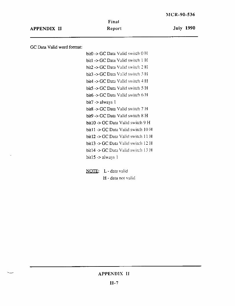
APPENDIX II
Final
Report
MCR-90-536
July 1990
GC Data Valid word format:
Valid switch 0 H
Valid switch 1 H
Valid switch 2 H
Valid switch 3 H
Valid switch 4 H
Valid switch 5 H
Valid switch 6 H
bit0 -> GC Data
bit1 -> GC Data
bit2 -> GC Data
bit3 -> GC Data
bit4 -> GC Data
bit5 -> GC Data
bit6 -> GC Data
bit7 -> always 1
bit8 -> GC Data Valid sv,,itch 7 H
bit9 -> GC Data Valid switch 8 H
bitl0 -> GC Data Valid switch 9 H
bitl 1 -> GC Data Valid switch 10 H
bitl2 -> GC Data Valid switch 1 1 H
bitl3 -> GC Data Valid switch 12 H
bitl4-> GC Data Valid switch 13 H
bitl5 -> always 1
NOTE: L - data valid
H - data no_ valid
APPENDIX II
II-7

APPENDIX II
Final
Report
MCR-90-536
July 1990
Sensorword Format:
bit0 -> sensor data bit 4
bitl -> sensor data bit 5
bit2 -> sensor data bit 6
bit3 -> sensor data bit 7
bit4 -> don't care
bit5 -> don't care
bit6 -> don't care
bit7 -> always 1
bit8 -> sensor data bit 0
bit9 -> sensor data bit 1
bitl0 -> sensor data bit 2
bitl 1 -> sensor data bit 3
bitl2 -> don't care
bitl 3 -> don't care
bitl4 -> don't care
bitl5 -> always 1
A current/voltage sensorword_set consists of 9 sensorwords of the above
format for a given current/voltage sensor. The 9 sensorwords will be of the following
order:
V rms
I rms
V offset
I offset
V instantaneous
I instantaneous
P instantaneous
P real
frequency
APPENDIX II
II-8
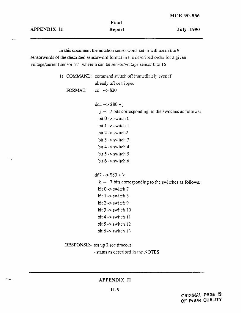
APPENDIX II
Final
Report
MCR-90-536
July 1990
In this document the notation sensorword set n will mean the 9
sensorwords of the described sensorword format in the described order for a given
voltage/current sensor "n" where n can be sensor/voltage sensor 0 to 15
1) COMMAND:
FORMAT:
command switch off immediately even if
already off or nipped
cc --> $20
ddl
J
bit 0 ->
bit 1 ->
bit 2 ->
bit 3 ->
bit 4 ->
bit 5 ->
bit 6 ->
--> $80 + j
-- 7 bits corresponding
switch 0
switch t
switch2
switch 3
switch 4
switch 5
switch 6
to the switches as follows:
dd2 --> $80 + k
k -- 7 bits corresponding to the switches as follows:
bit 0 ->
bit 1 ->
bit 2
bit 3
bit 4
bit 5
bit 6
switch 7
switch 8
-> switch 9
-> switch 10
-> switch 11
-> switch 12
-> switch 13
RESPONSE:- set up 2 sec timeout
- status as described in the NOTES
APPENDIX II
1I-9
PAGE 12
QUALITY

APPENDIX II
Final
Report
MCR-90-536
July 1990
2) COMMAND:
FORMAT:
command switch on immediately even if already
on or tripped
cc --> $21
ddl --> $80 +j (j is defined in (1))
dd2 --> $80 + k (k is defined in (1))
RESPONSE: - set up 2 sec timeout
- status as described in the NOTES
APPENDIX II
II.10

APPENDIX II
Final
Report
MCR-90-536
July 1990
3) COMMAND:
FORMAT:
reset switch
cc --> $22
ddl --> $80 + j
dd2 --> $80 + k
(j is defined in (1))
(k is defined in (1))
RESPONSE: - set up 2 sec timeout
- status as described in the NOTES
APPENDIX II
II-11

APPENDIX II
MCR-90-536
Final
Report July 1990
4) COMMAI_ D:
FORMAT:
RESPONSE:
select GC (all GC select codes will be set to zero)
cc --> $23
ddl --> $86
dd2 --> $85
- set up 2 sec timeout
- status as described in the NOTES
APPENDIX II
II-12

APPENDIX II
MCR-90-536
t, inal
Report July 1990
5) COMMAND:
FORMAT:
RESPONSE:
execute SIC fire, ware reset (does not reset actual set
configuration)
cc --> $24
ddl --> $80
dd2 --> $80
- set up 2 sec timeout
- four bytes of data plus the status as described in
the NOTES where the first two bytes give the
following data:
bit 0 -> 0 ifGC0 connected, 1 if not
bit 1 -> 0 if GC1 connected, 1 if not
bit 2 -> 0 if GC2 connected, 1 if not
bit 3 -> 0 if GC3 connected, 1 if not
bit 4 -> 0 if GC4 connected, 1 if not
bit 5 -> 0 if GC5 connected, 1 if not
bit 6 -> 0 ifGC6 connected, I if not
bit 7 -> always 1
bit 8 -> 0 if GC7 connected, 1 if not
bit 9 -> 0 if GC8 connected, 1 if not
bit 10 -> 0 ifGC9 connected, 1 if not
bit 11 -> 0ifGC10connected, 1 if not
bit 12 -> 0 ifGC11 connected, 1 if not
bit 13 -> 0ifGC12 connected, 1 if not
bit 14 -> 0ifGC13 connected, 1 if not
bit 15 -> always 1
APPENDIX II
II-13

APPENDIX IIFinal
Report
MCR-90-536
July 1990
the third byte gives the following data:
bit 0
bit 1
bit 2
bit 3
bit 4
bit 5
bit 6
bit 7
-> current SIC switch0 setting
-> current SIC switch1 setting
-> current SIC switch2 setting
-> current SIC switch3 setting
-> 0 if A/D connected, 1 if not
-> don't care
-> don't care
-> always 1
the fourth byte gives the following data:
bit 0 -> don't care
bit 1 -> don't care
bit 2 -> don't care
bit 3 -> don't care
bit 4 -> don't care
bit 5 -> don't care
bit 6 -> don't care
bit 7-> always 1
L_
APPENDIX II
11.14

APPENDIX lIFinal
Report
MCR-90.536
July 1990
6) COMMAND:
FORMAT:
RESPONSE:
reset continuous buffer
cc --> $25
ddl --> $80
dd2 --> $80
- set up 2 sec timeout
- status as described in the NOTES
APPENDIX II
II-15

APPENDIX II
MCR-90-536
Final
Report July 1990
7) COMMAND: fill continuous buffer (First use reset continous buffer
then use this command to download code that is to be
continuously executed. Code will start executing as
soon as the download is started. Up to 80 of these
commands may be concatenated before the buffer space
is overrun.)
FORMAT:
RESPONSE:
cc --> $26
eel --> $80 + q
ee2 --> $80 + r
(q is defined as higher 4 bits of
8-bit code(see sensorword))
(r is defined as lower 4 bits of
8-bit code (see sensorword))
At the end of the command is appended a $26
until the last command, then a SOD is appended.
- set up 2 sec timeout
- status as described in the NOTES
APPENDIX
11-16
II

APPENDIX II
MCR-90-536
Final
Report July 1990
8) COMMAND:
FORMAT:
fill once buffer (This command is used to download
code that is to be executed only once. Code execution is
started by the trigger once buffer command. Up to 80 of
these commands may be concatenated before the buffer
space is overrun.)
cc --> $27
eel --> $80 + q (q is defined as (13))
ee2 --> $80 + r (r is defined in (13))
ee3 --> as defined in (13)
RESPONSE:
At the end of the of the command or commands is
appended a SOD.
- set up 2 sec timeout
- status as described in the NOTES
APPENDIX II
11-17

APPENDIX IIFinal
Report
MCR-90-536
July 1990
J
9) COMMAND:
FORMAT:
RESPONSE:
-->
get buffered data
cc --> $29
ddl --> $80 + v
(v is defined as:
bit0
bitl
bit2
bit3
bit4
bit5
bit6
dd2 --> $80
-> buffer0
-> buffer 1
-> buffer2
-> buffer3
-> don't care
-> don't care
-> don't care)
- set up 2 sec timeout
- data of the following format and status as described in
NOTES
HEADER- $20
$ssssss - three bytes of status
$8F - dip switch setting for SIC card
(if not $8F, SIC card not
installed)
$nnnn - position in loop counter
$kk - times through loop counter
$mm - breakpoint
$22 - start of data
14 switchwords plus 1 GC Data Valid word
APPENDIX II
II-18

APPENDIX IIFinal
Report
MCR-90-536
July 1990
NOTE: TM is temperature
multiplexed, TC is
temperature common
(TM is not useful)
temperature sensorwords 0TM,
0TC, 1TM, 1TC, 2TM,
2TC, 3TM, 3TC
frequency sensorword 0
sensor_word_set_0
frequency sensorword 1
sensor_word set 1
frequency sensorword 2
sensor_word set 2
frequency sensorword 3
sensor_word set 3
$22 - end of buffer
repeat arrowed sections for sensors
4 to 7, 8 to ll, and 12to15
APPENDIX II
11-19

APPENDIX II
Final
Report
MCR-90-536
July 1990
10) COMMAND:
FORMAT:
RESPONSE:
trigger once buffer
cc --> $2A
ddl --> $80
dd2 --> $80
- set up 2 sec fimeout
- status as described in the NOTES
APPENDIX II
11-20

APPENDIX II
MCR-90-536
Final
Report July 1990
11) COMMAND: get power factor and sign (To calculate the power factor
use pfl=[Pavgl/[Vrmsl*Irmsl]. Use the same
calculation to determine pf2 using Pavg2, Vrms2, and
Irms2; if pf2 < pfl denotes capacitive loading; if
pf2>=pfl denotes'ind uctive loading; ie, voltage leading
current)
FORMAT: cc --> $2B
ddl --> $80 + j
dd2 --> $80
(j is defined as 0 to $F depending
on sensor pair used)
RESPONSE: - set up 2 sec timeout
- data defined as six sensor words for the specified in the
following order plus status as described in the
NOTES.
V mas 1
I rmsl
P reall
V rms2
I rms2
P real2
APPENDIX II
II-21

APPENDIX II
MCR-90-536Final
Report July 1990
12) COMMAND:
FORMAT:
RESPONSE:
get data for one specified switch a specified
number of times
cc --> $2C
ddl --> $80 + j (j is defined as 1 to $7F depending
on the number of times data
is specified to be taken -- input
buffer must be taken into account)
dd2 --> $80 + k (k is defined as 0 to $D depending
on the switch specified)
-set up 2 sec timeout
- data defined as:
j number of 16-bit switchwords plus the status as
described in the notes
_.,u,,_p ¢
APPENDIX II
II-22
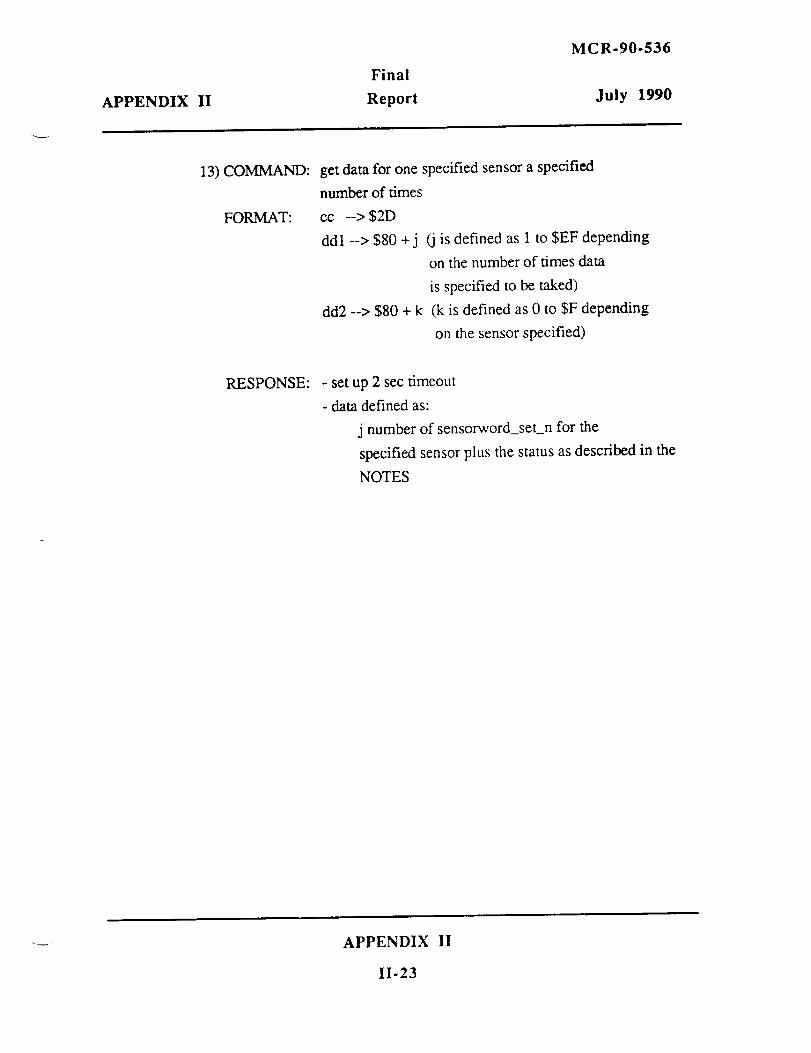
APPENDIX II
Final
Report
MCR-90-536
July 1990
13) COMMAND:
FORMAT:
RESPONSE:
get data for one specified sensor a specified
number of times
cc --> $2D
ddl --> $80 + j
dd2 --> $80 + k
(j is defined as 1 to $EF depending
on the number of times data
is specified to be taked)
(k is defined as 0 to $F depending
on the sensor specified)
- set up 2 sec timeout
- data defined as:
j number of sensorword set n for the
specified sensor plus the status as described in the
NOTES
APPENDIX II
11-23
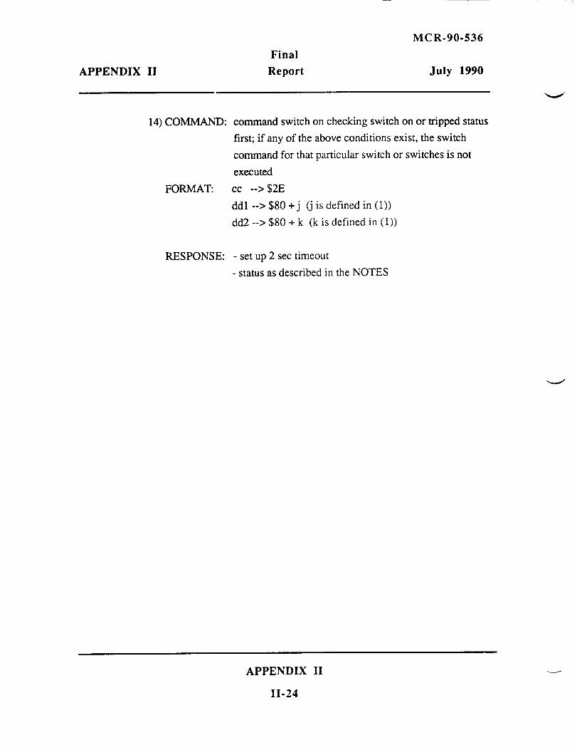
APPENDIX II
MCR.90-536
Final
Report July 1990
14) COMMAND:
FORMAT:
command switch on checking switch on or tripped status
first; if any of the above conditions exist, the switch
command for that particular switch or switches is not
executed
cc --> $2E
ddl --> $80 +j (j is defined in (1))
dd2 --> $80 + k (k is defined in (1))
RESPONSE: - set up 2 sec timeout
- status as described in the NOTES
APPENDIX II
11-24
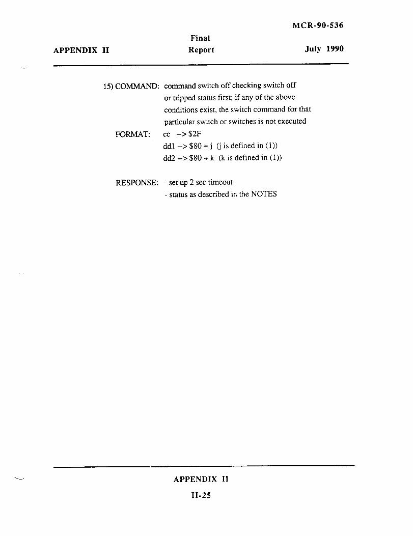
APPENDIX II
Final
Report
MCR-90-536
July 1990
15) COMMAND:
FORMAT:
command switch off checking switch off
or tripped status first; if any of the above
conditions exist, the switch command for that
particular switch or switches is not executed
cc --> $2F
ddl --> $80 +j (j is defined in (1))
dd2 --> $80 + k (k is defined in (1))
RESPONSE: - set up 2 sec timeout
- status as described in the NOTES
APPENDIX II
II-25

APPENDIX II
MCR-90-536
Final
Report July 1990
16) COMMAND: get data for all fourteen switches a specified number of
times.
FORMAT: cc --> $30
ddl --> $80 + j
dd2 --> $80
(j is defined as 1 to $7F depending on
the number of times data is specified to
be taken, input buffer size must be
taken into account)
RESPONSE: - set up 2 sec timeout
- data defined as:
(j times ( fourteen switchwords plus
GC Data Validword set)) plus the
status as described in the NOTES
APPENDIX II
II-26

APPENDIX IIFinal
Report
MCR-90-536
July 1990
17) COMMAND:
FORMAT:
RESPONSE:
get data for all sixteen sensors one time
cc --> $31
ddl --> $80
dd2 --> $80
- set up 2 sec timeout
- data defined as:
sixteen sensorword set n plus status
as described in the NOTES
APPENDIX
II-27
II
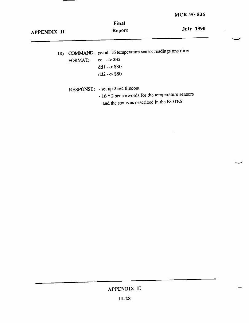
APPENDIX II
Final
Report
MCR-90-536
July 1990
18) COMMAND:
FORMAT:
RESPONSE:
get all 16 temperature sensor readings one time
cc --> $32
ddl --> $80
dd2 --> $80
- set up 2 sec timeout
- 16 * 2 sensorwords for the temperature sensors
and the status as described in the NOTES
APPENDIX II
II-28
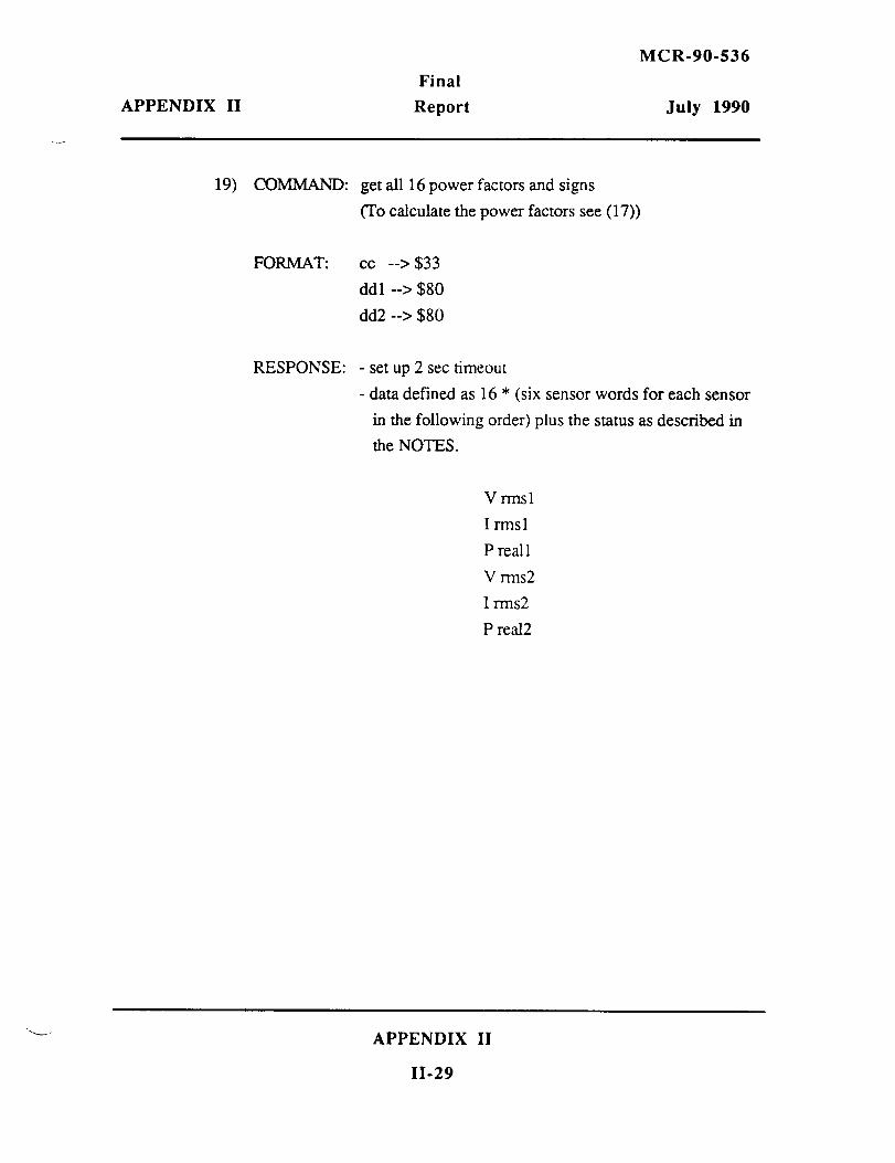
APPENDIX IIFinal
Report
MCR-90-536
July 1990
19) COMMAND:
FORMAT:
RESPONSE:
get all 16 power factors and signs
(To calculate the power factors see (17))
cc --> $33
ddl--> $80
dd2--> $80
- set up 2 sec fimeout
- data defined as 16 * (six sensor words for each sensor
in the following order) plus the status as described in
the NOTES.
V rmsl
I rmsl
P real1
V rms2
I rms2
P real2
APPENDIX II
II-29


MCR-90-536Final
APPENDIX III Report JuLY 1990
APPENDIX 1II
20 kHz AC Remote Power Controller Equipment Specification Document
This equipment specification document describing the operation of a 20 kHz AC Remote
Power Controller was prepared for reference use only by Martin Marietta and does not specifically
refer to the breadboard units developed for the SSM/PMAD.
APPENDIX III
I:I:1--I

..._,J

REVISIONS
DESCRIPTION OATE
(APeR
!
!
i
OF._" ,_GE IS
OF PO_._,'<QUALITy
OATIE
9-13-86
PAOJE:CT
,i-_
CON _r Igl AC lr _0..
,L_
__ _.L_J__ _ __J__ __J_____.MARTIN MARIETTA CORPORATION
DENVER AEROSPACE. POST OFFICE 8DE 179. DENVER. COLORJ_X)
KHZ AC" REHOTE PONER CONTROLLER
REV s'rA
OF _"4 E E
80201
SfZE "F $C _.1 ,'_O.
A 04236
sc"_c.II3:- 2 j
OwG NO
I_S.R ,' ^875CR 215950 I
S_EET


SYM PAGE
REVISIONS
DF_CRIPTION DATE APPROVED
CHG
SIZE
SCALE
COOE IDENT NO.
PAGE
MARTIN MARIETTA CORP.
NSR/A875CR215950
SHEET!
.zzT-_


TABLE OF CONTf-INTS
Page No.
L.O
l.l
t.2
2.0
2.1
2.1.t
2.l.2
2.1.3
3.0
3.1
3.2
3.2.1
3.2.2
3.2.3
3.2.4
3.2.5
3.2.6
3.3
3.3.1
3.3.2
3.3.3
3.3.4
3.3.5
3.3.b
3.3.7
3.3.8
3.3.9
3.3.1.1.
3.3.1`2
3.3.13
3.4
SCOPE ................................................. 4
Ge nera i ............................................... 4
Class£ficacion ........................................ 4
APPL[CASLE DOCUMENTS .................................. 5
Gene ra 1 .̀.............................................. 5
Spec _ f Lcac ions ........................................ 5Standards ............................................. b
Ocher Publicac ions ..................................... 7
REQUIREMENTS .......................................... 8
teem DeEiniCion ........................................
Characteristics .......................................
Performance Characteristics ........................... 8
Physical Characteristics .............................. 1`3
Reliabi1`icy ........................................... 13
Ha_nCainabi1.iCy ....................................... 1.4
Env_rorumenCa1. Requirements ............................ 14
Transporcabi1.iCy ...................................... 26
Design and Construction ............................... 2b
Parts, Materials, and Processes ....................... 2b
E1.eccromagneCic InCer£erence (EHI) .................... 2bNamep1.aces and Produce Harkings ....................... 28
Workmanship. 28
Incerchangeab_1.icy and Replaceab_1.icy ................. 28
Safety ................................................ 29
Human Performance�Human Enginering .................... 29
Structural Integrity .................................. 29Pos it ive-locking Devices .............................. 30
D_mens_on_ng and To1`eranc_ng .......................... 30Produce C1.eanliness ................................... 30
Design for Test ....................................... 31.
Supplier Documentation ................................ 32
0[52b FSCH NSRS _75CR215950
0_23o Sheet 2 Rev [
!I]I-H

-._,¢
v

4.0
4.t
4.1.1
4.L.2
4.1.3
4.1.4
4.2
4.2.L
4.2.2
4.2.3
4.3
4.3.L
4.3.2
4.3.3
4.3.4
5.0
b.O
tAbLE OF CONTENTS (cont'd)
QUALITY ASSURANCE PROVISIONS ..........................
l'a_e No.
33
General. 33
ResponsibiLity for Ver[EicacLon ....................... 33
QuaLity Assurance ..................................... 33Not[f[caCLon of Tests ................................. 33
Test Program ControLs ................................. 33
QuaL[cy Conformance VerifLcat:_on ...................... 34
Ver£f£caC£on Methods .................................. 34
Test Category DeEin[C[ons ............................. 34
Test Types ............................................ 35
Test Requirements ...................................... 35
Development Tests ..................................... 35
Acceptance Tests ...................................... 36Qual£ficat£on Tests ................................... 3_Certification ......................................... 40
PREPARATION FOR DELIVERY .............................. 41
NOTES ................................................. 43
TABLES ................................................ 45
FIGURES ................................................ 47
0L52b FSCM NSRS o75CR215950
O423_ Sheet 3 Rev L

-,,wl

; . 0 SCOPF.
[.l General Thi._ Drawing establishes tile design, construction, per(ormance,
a.d veci/icacion requirements for Remote Pouer ControLler. liereina[cer _he
Remote Power Controller is re_erred co as the RPC.
L.2 Classification The RPC shall be designated by ConCrol[ing SpecificationNumber(s) as _ol[ows:
DASH NUHBER
_15CR215950
NOMENCLATURE
20 Khz AC Remote Power ControLLer
.'; t,,_ %,_
OF POOR QUALITY
OlS2b FSCM
O_23b
NSRS _75CR2[59S0
Sheet & Rev t


2.0 APf' 1. [CAlll.['i [)OCUNH N'FS
2.1 General The following documents of the exact issue shown shall form partof this drawing to the extent specified herein. When an exact issue is not
specified, the applicable issue sl_ll he as required In the Procurement
Agreement. In case of conflict between the requirements of this draw_ns and
any referenced document, the requirements of this drawing shall govern.
2.1.1 Specifications
2.1. i.i Federal
2.1.1.2 Milltary
MIL-B-5087B
15 Oct 64
Int Amend 3
24 Dec 84
Amend 2
31 Aug 70
Bonding, Electrical and Lightning
Protection for Aerospace Systems
HIL-P-9024G
06 Jun 72Packaging, Handling and TransportabilityIn System/Equipment Acquisition
MIL-A-21180D
05 Nov 84Aluminum Alloy Casclngs, High Strength
3.1.1.3 Other
SP-R-O0 22A
9 Sept 74
MSFC-STD-512A
Ol Dec 76
NASA RP-I024
July 1978
JSC 30000
MSC S-M-O003
SS-SRD-O001
Vacuum Stability Requirements of Polymeric
Macerlals for Spacecraft Applications.
Man/System Requirements for
We lghtless Envtroments
Ant hropometrlc Sourcebook
Space Station Program Deginf.t_onand gequi remenCs
Design Requlrements/Mauned Spacecraft
and Related Flight Crew Equipment
Markings, Labllng and Color
OF POOR QUALrl'y
0152b FSCM
0_ 2 36
NSRS 87 5CR21 59 50
Shoet 5 Rev I
.III-7

,_u _-
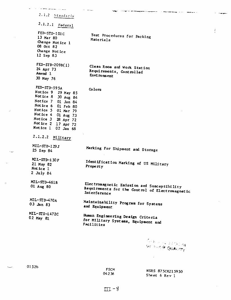
2. 1.2 ._tan,l_r,:s
2.1.2.1 Fedenal
FED-STD-1 O1 C
13 Mar 80
Change Notice 108 Oct 82
Orange Not ice12 Sep 83
FED-STD-209B(I)
24 Apr 73Amend 1
30 May 76
FED-STD-59 5A
Notice 9 29 May 85
Notice 8 30 Aug 84
Notice 7 01 Jan 84
Notice 6 01 Feb 80
Notice 5 01 Mar 79
Notlce 4 01 Aug 73
Notice 3 28 Apr 72
Notice 2 17 Apt 72Notlce 1 02 Jan 68
2.1.2.2 MiL_tar 7
MIL-STD-129J
25 Sep 84
MIL-STD-130 F
21 May 82
Notice 1
2 July
MIL-STIY-461B
01 Aug 80
MIL-STD--470A
03 Jan 83
MIL- STD-1472C
0 2 May 81
Test Procedures for Packing
Mate rta is
Clean Room and Work Station
Re qul reme nt s, Co nt rol ledEnvi ronm ent
Colors
Marking For Shipment and. Storage
Identification Marking of US Military
Prope rt y
Electromagnetic Emission and Susceptibility
Requirements for the Control of Electromagnetic
Interference
Maintainability Program for Systems
and Equipment
Human Engltmering Design Criteria
for Mllitary Systems, Equipment andFacilities
0152b FSCM
04236
NSRS 875CR21 59 50
Sheet 6 Rev I


.....
T
,MI/.-STD-1522A
28 May 84
Not ice 1
21 Dec 84
Standard Cenecal Requtcements For
Safe Design and Operation of
Pressurized Mtsslle and Space
Systems
MS33540G
09 Feb 73
Safety Wlrlng, and Cotter Plnnlng,General Practices for
2.1.2.3 Indu st ry
ANSI YI4.5H
1982
Dimensioning and Toleranclng
ANSI Y32.2
1975Graphic Symbols for Electrical and
Electronics Diagrams
ANSI %'32.16
1975
Reference Designations for Electrical
and Electronics Parts and Equipment
2.1.2._ Occupat Ional
2.1.3 Other Publications
2.1.3.1 Manuals
2.1.3.2 Re_ulatlons
2.1.3.3 Handbooks
1
/
MIL-HDBK-5 D
I Juu 83
Vol 1
Not ice i
i Jan 84
Vol 2
Not Ice 2
i Jan 84
Metallic Materials and Elements for
Aerospace Vehicle Structures
NHB 6000. iC Requirements for Packaging, Handling and
Tr_nsportatlon for Aeronautical and Space
Systems Equipment and Associated Components
2.1.3.4 Martin Marietta Denver Aerospace
M-67-45
Revision 3
Dec 83
Test Methods and Controls
Components
SSP-MMC-O00 20
WP-01
Vol i
Systems Test and VerificationPlan
-v 0152b FSCH
042 36
NSRS 87 5CR2159 50
Sheet 7 Rev I

3. [ [te,n Definitio,I. A RPC is a solid scare remote power controller a,,d a
circuit monitoring and protection device. This specification defines the
requirements of solid scare RPC for use in proCecCing Cl_e 20d Vac, 20 KHz
electrical distribution system from overloads and faults. The RPC covered bychis specification will be used fo_ proCeccion of BUS feeders as well as the
wiring Co individual loads. Coordination between RPC's of differing racing is
required. RPC operation shall be trip free. RPC shall be capable of GroundFault interrupt ion.
3.2 Characteristics The R.PC shall be SPST and shall be designed co actuate
by means of logic level signal applied co the on and off control J.npucs. The
RPC control inputs will also have a inhibit and data enable descri.bed herein.
These inputs will be from open collector sou.rces wlch a maximum 36V off scare
voltage, sinking capability of 10 mA in che low scare and a maximum leakage
current of lO0 uA in the high scare. A tripped device shall be reset by
removing and reappl I Che control signal.
The RPC capab 'ng a latching type load
isolation relay which will electrically isolate the load by switching the
relay off after the R.PC has turned off. Similarly, the RPC shall turn the
relay on prior Co _niciacing iCs normal turn on function. Two RPCs shall be
compatible in forming a break-before-make SPDT switch. The control circuit
shatl be electrically isolated from the power circuits _ol circuitry
will receive power from the primary line.
3.2.1 Performance Characteristics. The performance characteristics of the
RPC shall be as specified in the (_ollowing paragraphs.
3.2.l.I Power
3.2.1.I.i Power input. The P,PC shall meeC the requirements of this drawing
when operating on input power with the following characteristics:
0 t52b FSC._
0423o
NSRS d75CR215750
Sheer 8 Rev [

.:,___T • ,
SC.'t_on and I'_.aC_ot'.t
Frequency
Vo l Cage
20 KHz +/- . 5% Ilz
Load Power Factor
20e_ Vrms +/- 2.5Z ac Modules and
ac¢ached payloads
0.9 Min
Total Harmonic 3%
Distortion
3.2.t.l.l.l
Maximum amplitude: 3cd
harmonic 30 db below
fundamental. 5Oh harmonic
(TBS) db below fundamental
Power Consumption
Switch Currents 3ma ac 20_ Vac 20 Khz
(switch off with raced load connected)
Supply Current
(100% rated load)
Load current +3mA
aC 208 Vac 20 KHz
(
Ot52b FSCM
0423b
NSRS 675CR215950
Sheet 9 Rev [
.Ill-it

,\) Switch Form
IS) Trip Characteristics
C) Switch Ratings
D) Overload Trip
E) Fault Trip
F) Peak Lec-thru current
C) Rupture Current
H) On-sCare voltage drop
I) Power Dissipation*
J) Turn-on/turn-off delayK) Turn-on
L) Turn-off
H) Initial Turn-on or restart
current limit
N) Initial Turn-on or restart
time delay
SPST
Figure 1.
Table b
l.l x Rating
(Figure l)
&.3 x racing (r_ix) w_thin 5ms.
4.3 x racing <max)
UnLimlted (current Limited)
L.lS Vac (max)
IX of VA rating (max)
2.5 ms (Hax)
wit:hin 2uS of zeco
within 2uS of zero current
2.25+ .25 x rating
50+ 5 msec to 5+ .5 sec
seTectabte
* A design goal is to minimize the power dissipation in the RPC power stage.
3.2.L.3. Trip Characteristics (Figure 1)
3.2. L.3.L Overload The RPC shall automatically attempt a second start-up any
time the toad current exceeds the time/current envelope of Figure l.
3.2.L.3.2 Initial Turn-On The RPC shall lim_c the inrush curent to 225Z+ 25X
of its racing for a fixed time delay during initial turn-on or re-start. The
fixed time delay shall be adjustable from a minimum of 50 milliseconds to 5
seconds maximum. An external capacitor may be used Co set the rime delay. An
external resistive element may also be used in order co minimize the heat
dissipation internal Co the RPC in the current limit mode.
3.2.t.3.3 Load Faults The RPC shall provide load fault verification and fuse
backup in the event that the trip circuit fa_Ls to operare.
3.2. L.3.4 Reset
O_F then ON.
A tripped RPC shall be reset by cycling the control signals
3.2.l.3.5 Ground Fault A common mode current on the input power Lines
exceeding 50 mA £or 60 mS shall cause the RPC to trip off.
3.2.l.3.b Power Supply Surges A power supply surge that results in a current
surge that exceeds the trip curve of Figure I shall result in the RPC
automatically restarting its turn-on sequence.
f
Rs_, _ p._,_S ISOF POOR QUALITY
0 L52b FSCH
042 3 o
NSRS _5CR21595{}
Sheet 10 Rev l
2!I-)2-

_.'!. L. I. 1 i',,_,.'r ,t[_j_L_' l_t.Lcka, lt ,\ I._,._" supply Chat dr,_p_ below LSO voL_._[¢Jr .u_v.: th:l=l 2.3 vniLL_seconds six:nil ¢a,,._,: the RPC to switch off at the
sul_seq,,e_lt zero cucrcoC cross{n g. When the power supply returns to ,1oriel,
el... RPC shnt| auto_t{catly restart _cs turf_-ou sequence.
3.2.[.4 Coatrot Circuits
3.2.'L.4.l Logic Levels Logic levels shall be as noted in the following cable:
Logic State Logic Level Logic VoLtase.
Low 0
High l
-0.5 to +2.5 Vdc
+3.5 to +3b Vdc
Output circuits shall be of the "open collector" type capable of sinking -LO
mA in the LOW state and having a maximum Leakage current of -LO0 uA _n the
HIGH state (with 36 Vdc applied through a 3bOO ohm resistor). Input circuits
shall be capable of interfacing with TTL, C_OS or open cotLecco_ circuits.
For open collector inputs, the in_ernal pull-up circuit shall be capable of
supplying at Least lO0 uA _n che HIGH state. The LOW scare sink current shall
not exceed lO n_.
3.2.L _.2 ON/OFF Control Inputs The RPC shall have separate ON and OFF
_npuCs _hac control _he RPC_s power switch as described in _he following cable:
/
ON ¢nput OFF Input RPC Status
0 0 ON
0 1 ON
l 0 OFF
l 1 NO CHANGE
Each input shall be capable o_ accepting either a continuous or a pulsed togLc
LOW _npu_. For a pulsed input, the minimum pulse width shal_ be 10
m{lL_seconds w_th a r_se and fall cLme of less Chat l m_ll_second.
3.2.1.4.3 INHIBIT _npuc The INHIBET input shall turn off the RPC's power
switch but shall not change the state of the Lncernal Latch set by the ON/OFF
_npu_s.
[nhLbic Inpu_ RPC Response
LOW Scare
HIGH Sta_e
Power Switch _nhibited
Power Switch Enabled
3.2.1.4.4 DATA ENABLE The RPC shall generate a serial da_a output as
described _n paragraph 3.2.L5.2 in response to the DATA ENABLE and CLOCK
inputs. Refer to F_.gure 5.
Data Enable Input RPC Response
LOW Scare
HIGH ScaCe
Data Latched (I)
Data Unlatched, R_PC reset (2)
O t 52b FSCH
04230
NSRS _75CR215950
Sheet L l Rev 1
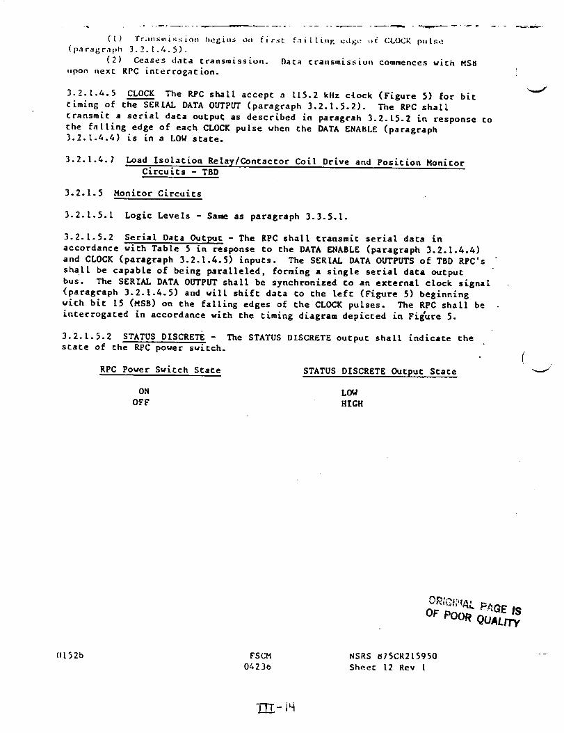
. . . ...... ° ....... _ .....
(L) Tr.,._,.[._sLo. l_gi,,s o. fi¢'_c faiLL[.g cd_e -{ CL.OC_ put._e
(p._ragraph 3.2. t./0.5).(2) Ceases data transm_.ssLoll. _ata Crallsm[ssiui1 Commences w[ch MSB
,,pon next RPC interrogation.
3.2.t.4.5 CLOCK The P.PC shall accept a tlS.2 kHz clock (Figure .5) for bit
timing of the SERIAL DATA OUTPUT (paragraph 3.2. t.5.2). The RPC shall
transmit a serial data output, as described in paragcah 3.2.l.5.2 in response to
the falling edge of" each CLOCK pulse when the DATA ENAI_LE (paragraph
3.2.t.4.&) is in a LOW star.e.
3.Z.l.4.7 Load Isolation Rela_/Concactor Co_l Dc_ve and PositLon MonitorC_rcu_Cs - TBD
3.2. L.5 Monitor Circuits
3.2.L.5.1 Logic Levels - Same as paragraph 3.3.5.1.
3.2.L.5.2 Serial Data Output - The RPC shall transmit serlal data _n
accordance w_th Table 5 _n response to the DATA ENABLE (paragraph 3.2. L.4.4)and CLOCK (paragraph 3.2.l.4.5) inputs. The SERIAL DATA OUTPUTS of TBD RPC's
shall be capable of being paralleled, forming a s_ngle serial data output
bus. The SERIAL DATA OUTPUT shall be synchronized to an external clock signal
(paragraph 3.2.1.4.5) and will sh_ft data Co the Left (Figure 5) beginning
w[Ch b_c L5 (MSB) on the falling edges of the CLOCK pulses. The RPC shall be
Lnterrogaced _n accordance with the C[m£ng d_agram depfcced in Figure 5.
3.2.1.5.2 STATUS DISCRET_ - The STATUS DISCRETE output shall indicate the
scare of the RPC power switch.
RPC Power Switch State STATUS DISCRETE Output State
ON LOW
OFF HIGH
/
OF POOR QUAL/Ty
O [52 b FS CM
042]0
NSRS o/SCR2L5950
Sheet L2 Rev I
-jr
u! i .X :
I.
2.
3.
/.,.
Ri'(] L,),l,d._ - "l'JI,L" I,:l'l; sh.ll ] I),' L:,li).e!,[." ,,! p(J_,',*r=,l_ r_l ,_, ',.,)[ [_)wi.,ig [o;l..I
I,l,,SiSt:iw_" loads
[n(hJctive Loads
20 kllz transformers
Off=Line ))ridge rectifLers (Figure _,)
3.2.2 Ph)tsica l Characteristics
3.2.2. L Size and ConfiFuuratLon The size, configuration and mount:ing
dimensions shall be in accordance with r.he requiremenr.s of figure TBO (see
3.3.L1 herein - dimensioning and toLerancing).
3.2.2.2 Weight The RPC shall be designed co a minimum weight buC shall not
exceed .b Lb. for a L5 amp RPC.
3.2.2.3 Hountinp_ The RPC shall operate as specified herein when mounted in
any orientar_ ion.
3.2.2.4 ELectrical [nterface. The electrical interface diagram for the RPC
is shown in Figure 2.
3.2.3 Reliability
3.2.3.1 DesJ._n RecluJ.remencs Reliability requirements:and cr£teri.a shall be
established and incorporated into the design. The effective implementation of
these requirements shall be accomplJ.shed as specified herein.
3.2.3.2 Supplier Reliability Program. The supplier shall establish a
reliability program that meets Ehe requirements of JSC 30000, Section 9,
paragraph 3.0. The reliability program shall be an integral part of the
supplier's design, development, test and operational activities.
3.2.3.3 Field Reliability The RPC shall achieve a meantime between failures
(MTBF) of at Least TBS hours. The MTBF shall be based on an operating time of
TBS hours per year and a non-operating (standby) time of TBS hours per year.
If redundancy is required Co achieve the specified reliability it shall be
subject to Martin Marietta approval.
_._ ' _-_ ,_-_
Ot5"2b FSC_t NSRS _75CR215050
Sh,.,.: 13 R,:v I

3.2.3.4 Fa[ lure To ' e rance N/A
3.2.3.5 Failure Propagation The RPC destgn shall he such Clot one failuredoes noc cause additional falluces.
3.2.3.6 Service Life The RPC shall remain operational 10 years hefoce
replacement ls needed.
3.2.4 Maintainability Design for maintainability shall be in accordance wtchJSC 30000, Section 3, Part (TBD), (SSP-MMC-4TBD Matncainabllicy Implemencacton
Plan) and ($SP-MMC-4TBD Maintainability Design Guide). Design for
maintainability includes buc is noc limited co requirements for access,
mea_Ime Co repair (MTTR), fasteners, mousing interface and malncalnablllcy
veriflcaclon.
3.2.4.1 Malncenance Concept The maintenance concept Is specified in JSC30000, $ecclon 4, Part 4,
3.2.5 Environmental RequlremenCs
3.2.5.1 Ground storage, transportation and handling environments The
assembly shall meet the requirements specified herein after exposure In a
packaged (unless otherwise specified), non-operating condition to the
following envtronments.
3.2.5. I.i Temperature -55 ° to 65°C (-67°F to 149°F).
3.2.5.1.2 Pressure 20.6 kPa to ii0 kPa (3 psla to 16 psla)./
3.2.5.1.3 Relative Humidity 0 - 100%.
3.2.5.1.4 Salt fog 1% NaCl by weight, as defined In MIL-STD-810, method509.2, Procedure I.
3.2.5.1.5 _gus As identified in MIL-STD-810, method 508.3.
3.2.5.1.6 Ozone i0 parts per billlon by _lume.
3.2.5.1.7 l_necmal Radlatlon As defined tn MIL-STD-810, Method 505.2,
pcocedure I.
3.2.5.1.8 Sand and Dust TBD
3.2.5.1,9 Slnusoldal Vibration As defined in Marshall TM86538 Section VI,
Transpor_atlon and Handling Criteria and Procedures.
3.2.5.1.10 Acceleration (covered under 3.2.5.1.9 and 3.2.5.1.10.1).
015 2b F$CM
04 236
13:-
NSRS 875CR215950
Sheet 14 Rev 1
ORIGh_JAL P,_GE IS
OF P,_OR QOALn'Y
l
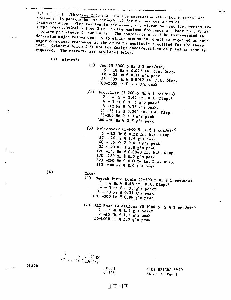
].2. 5. ]. ]O.i Vlbratlon Criteria The transportation v[b_atlon criteria are
presented In pa_'agraphs (,a) through (d) _or the various modes of
tt-ansporCaCion. When testing Is perfozlued, the vibration test frequencies areswept logarithmically from 5 llz. to the maxlm,,_ frequency and back to 5 llz at
I octave per minute In each axis. The components should be Instrumented to
determine major resonances. A 15 m£nute stnuso£dal dwell is requlred at each
major component resonance at the crlterla amplltude speclfled for the sweep
test. Criteria below 5 Ha ace for design consLderatlons only and no test ts
required. The criteria are tabulated below:
(a) Aircraft
(1) Jet (5-2000-5 Hz @ 1 oct/m£n)
5 -i0 Hz @ 0.022 In. D.A. Dlsp.
10 - 35 Hz @ 0.11 g's peak
35 -200 Hz @ 0.0017 In. D.A. Dlsp.
200-2000 Hz @ 3.5 O's peak
(2) Propeller (5-700-5 Hz @ 1 oct/m£n)
2 -4 Hz @ 0.42 In. D.A. Dlsp.*
4 - 5 Hz @ 0.35 g's peak*
5 -12 Hz @ 0.35 g's peak.
12 -55 Hz @ 0.045 In. D.A. D£sp.
55-300 Hz @ 7.0 g's peak
300-700 ttz _ 3.5 g's peak
(3) Hellcopl:er (5-600-5 Hz (_ 1 oct./rain)"
5 -12 Hz @ 0.22 in. D.A. Dlsp.
12 - 40 Hz @ 1.6 g's peak40 -55 Hz @ 0.019 g's peak
55 -120 Hz @ 3.0 g's peak
120 -170 Hz @ 0.0040 in. D.A. Dlsp.
170 -220 Hz @ 6.0 g's peak
220 -260 Hz @ 0.0024 in. D.A. Dlsp.
260 -600 Hz @ 8.0 g's peak
(b) Truck
(1) Smooth Paved Roads (5-300-5 Hz @ 1 oct/rain)
1 -4 Hz @ 0.43 in. D.A. Disp.*
4 - 5 Hz @ 0.35 g's peak*
5 -150 Ha @ 0.35 g's peak
150 -300 Rz @ 0.06 g's peak
(2) All Road Condttions (5-1000-5 Hz @ 1 oct/mln)
1 - 7 Hz @ 1.7 g's peak*
7 -15 Hz _ 1.7 g's peak
15-1000 Hz @ 1.7 g's peak
0152b FSCM
06 236
NSRS 875CR215950
Sheet 15 Rev I
/311-I-7

(c) ]'rains
(I) Normal Railroad operations (5-2000-5 llz _ I oct/rain)
2 - 3 Hz @ 2.6 tn.D.A. Disp.*
3 - 6 llz @ 1.2 g's peak*
6 - 130 Hz @ 1.2 g's peak
130 - 185 Hz @ 0.0014 in. D.A. D_sp.
185 - 2000 Hz _ 2.5 g's peak
(d) Ships
(I) Normal Shipping Operations (5-300-5 Hz @ 1 oct/mln)
0.1 - 0.3 Hz @ 0.35 g's peak _
0.3 - 1.5 ltz @ 0.35 g's peak t1.5 -4.0 Hz @ 0.i0 g'a peak*
4.0 - 5.0 Hz @ 0.12 in. D.A. D£sp.
5.0 - ii Hz @ 0.12 in. D.A. D£sp.
Ii - 300 Hz @ 0.75 g's peak
* Design criteria only, no test required.
3.2.5. I.Ii Shock As defined in Marshall TM86538 Section VI Transportation and
Handling Criteria and Procedure.
3.2.5.1.11.1 Shock Criterla r Transportatlon When shock testing is required
because of tall shipment the test should be conducted by applying five shocks
in each of three mutually perpendicular axes (15 shocks total). Any shock
pulse that results in a response spectrum (Q- i0) as severe as that presented
below will be acceptable.
Railroad Car [lumping Conditions (5 shocks per axis)
20 -160 ltz @ +6 dB/oct
160 - 340 liz @ 500 G's peak340 -400 l_ @ -6 dB/oct
3.2.5. i. II. 1 Transporcatlou Shock Handling Criteria and Procedures Handlingcrlterta are required to account for typical conditions that occur during
loading or unloading operations. Tests for these conditions consist ofnumerous container drops from various orientations of the container. Nhere
equipment design allows, equipment will be subjected to a transit drop test as
described below. If normal equipment deslgn does not allow this type testing,
the procedures and required protection in handling are to be submltted to the
appropriate MSFC program manager for approval.
3.2.5.1.11.2 Test Conditions The transit drop test should be used for
equipment in its transit or combination case as prepared for field use to
determine if the equiment is capable of withstanding the shocks normally
induced by loading ard unloading of equipment.
For equipment weighing I000 pounds or less, the floor or barrier receiving the
impact shall be of solid 2-in. thick plywood backed by either concrete or a
rigid steel frame. For equipment weighing over I000 pounds, the floor or
barrier shall be concrete or its equivalent.
O152b FSCM
O_ 236
EI-i8
NSRS 875CR215950
Sheet 16 Rev I
O^I_:,A,_ F;._3E'.IS
OF POOR QUALITY

_.2.5. I. 1t..: 'i','._t ;',_rfor_:u,:_ce Subject tl_ test ttem to the numl_r and_lgbt._ of ,Irop as tndlcated in Table 3.2.5.1.11./4-1. Prior to proceeding
with any of the test methods, the test Item shall be operated under standardambient conditions and a record made of all data necessary to determine
compliance with required performance. These data shall provide the criteria
for checking satisfactory performance of the test item, either during or at
the conclusion of the test, or both, as required.
Thale 3.2. 5.1.11.4-1
Welght and Test] Item and Case
] (pounds)'[ Under i00 lb.
Man-Packed and
Man-Po rtable
Largest He lght of
Dimensions Drop
(inches) Notes (inches)Under 36 A 48
36 & ore r A 30
Number of drops
I00 to 200 lb Under 36 A 30
Inclusive 36 & over A 24
Drop on each face, edge,and corner.
Total of 26 drops.
Drop or, each corner.
Over 200 to Under 36 A 24
i000 Ib 36 to 60 B 36 Total of 8 drops.
Inclusl ve Over 60 B 24
/
Over I000 No limit C 18 4 edgewise drop.
2 cornerwlse drops.
/Note A. Drops shall be made from a qulck-release hook or drop tester as made
by the L.A.B. Corporation, Skaneateles, New York, or equal. The test item
shall be oriented so that upon impact a llne from the struck corner or edge to
the center of gravity of the case and contents is perpendicular to the impactsurface.
Note B. Wlth the longest dimension parallel to the floor, the transit or
comb£naclon case with the test Item within shall be supported at the corner of
one end by a block 5 In. high and at the other corner or edge of the same end
by a block 12 in. high. The opposite end of the case shall then be raised to
the specLfled height at the lowest unsupported corner and allowed to fall
ftee ly.
Note C. While in the normal transit position, the case and contents shall be
subjected to the edgewise and cornerwise drop test as follows (if normal
transit position is unknown, the case shall he oriented such that the two
longest dimensions are parallel to the "floor').
Edgewise drop test. One edge of the base shall be supported on a sill 5 to 6
In. high. The oposlte edge shall be raised to the specified height and
allo_d to fall freely. The test shall be applied once to each edge of the
base of the case (total of four drops).
Ol 526 UP" _._(._q¢ t ,U.t!A,j_¢ r sc
04 2 36
NSRS 87 5CR21 59 50
Sheet 17 Rev 1
ZIE -lq

Cocnec_f.se drop test:: One corner of the base of the case sl_l[1 he_ support:ed
on a block approxlmacely 5 In. high. A block normally 12 In. high shall be
placed under th_ other corner of the same end. The opposite end of che case
shall be ra_sed to the speclfled helght at the lowest unsupported corner and
allo_d co fall freely. Thls test shall be applied once co each of two
diagonally opposlce corners of the base (coral of two cornerwlse drops). When
the proportions of wldch and height of the case ace such as to cause
inscab£1lty In the cornerwise drop test, edgewise drops shall be subsclcuced.
In such Instances two more edgewise drops on each end shall be performed (four
addltlonal edgewise drops for a coral of eight edgewise drops).
(b) Upon completion of the transit drop test, the test item shall be operated
and the results compared to data obtained prior co testing In accordance with
the following procedures. Prior co proceeding with any of the test mehtods,
the test Item shall e operated under standard ambient conditions and a recordmade of all data necessary co determine compliance with required performance.
These dar.a shall provide the criteria for checking saClsfactory performance of
the rest Item du_Ing tesclng or at the cbnclusion of the test or both, as
required. CErtlflcaclon by signature and data block is requlred.
(c) The test Item shall then be visually inspected and a record made of any
damage/deterloratlon resulting from the_ test. If a test chamber Is used for
the test, perform a vlsual inspection of the test Item w_chln the chamber at
test condlClons when possible. Upon completion of the test, vis_ally inspect
the test item again after the test item has been returned Co standard ambientcondltlons. Deterlorat_on, corrosion, or change In tolerance limits or any
internal or external parts which could in any manner prevent the test item
from meeting operational service or matntennance requirements shall be reason
to consider the test leer _s having failed to withstand the condltlo_s of thetest.
0152b FSCM
04 236
NSRS 87 5CR2159 50
Sheet: 18 Rev I
I-20OR[Gs;_'.;_oLPs_GE IS
OF POOR QUALITY

3.2.5.2 l.._..c' environment._ The assembly shall meet tl_ requirements of this
spectflcacion during and after exposuce co the {olLowtng launch env_ror_ents.
3.2.5.2.1 Module Interior
3.2.5.2.1.1. Tempecature +15.6 ° to 32.2°C (60°F co 90°F)
3.2.5.2.1.2 Pressure 100 to 013 kPa (14.5 to14.9 psia)
3.2.5.2.1.3 Humidity 1.7°C to 2_t°C dew points (35°F co 70°F)
3.2.5.2.1.4 Alrbocn NaC1 TBD
3.2.5.2.1.5 Fungus i000 coony forming units (CFU)/m 3.
3.2.5.2.1.6 Ozone 6 parts per billion by volume.
3.2.5.2.1.7 Sand and Dust TBD
3.2.5.2.1.8 Random Vibration See Figure 3.2.5.2.1.8-I through 3.2.5.2.1.8-2
for Input random vibration levels at attach polnc and for _he response load
factors as a function of fundamental frequency for design.
3.2.5.2.1.9 Acceleration Covered in 3.2.5.2.1.8 and 3.2.5.2.1.11.
3.2.5.2.1.10 Acoustics See Table 3.2.5.2.1.10-1.
. _ _._ _ "_
0152b FSCM
04236
NSRS 875CR215950
Sheet 19 Rev 1
-F I-21

i'".
Table 3.2.5.2.1.10-1
1/30c cave
Center Frequency(Hz)31.540
5063
80
100125
160200
250
320z.O0
500
630
800
1000
1250
1600
2000250032004000500063008000
10000OAL
Band Level (dB ce 2 x I0 -5N/n2)
111.0113.0116.0118.5120.0122.0124.0125.0126.5127.0127.0127.0
126.0
123.5
120.5
115.5
113.5
112.0
109.0
106.5
103.0i00.5
97.5
95.091.0
89.0136.0
TEST TIME: T_
ORIGIi_A{.PA_E ISOF PO_ QUAL/T'Y
0152b FSCM
04236
NSRS 87 5CR215950Sheet: 20 Rev 1
ZZZ-2_
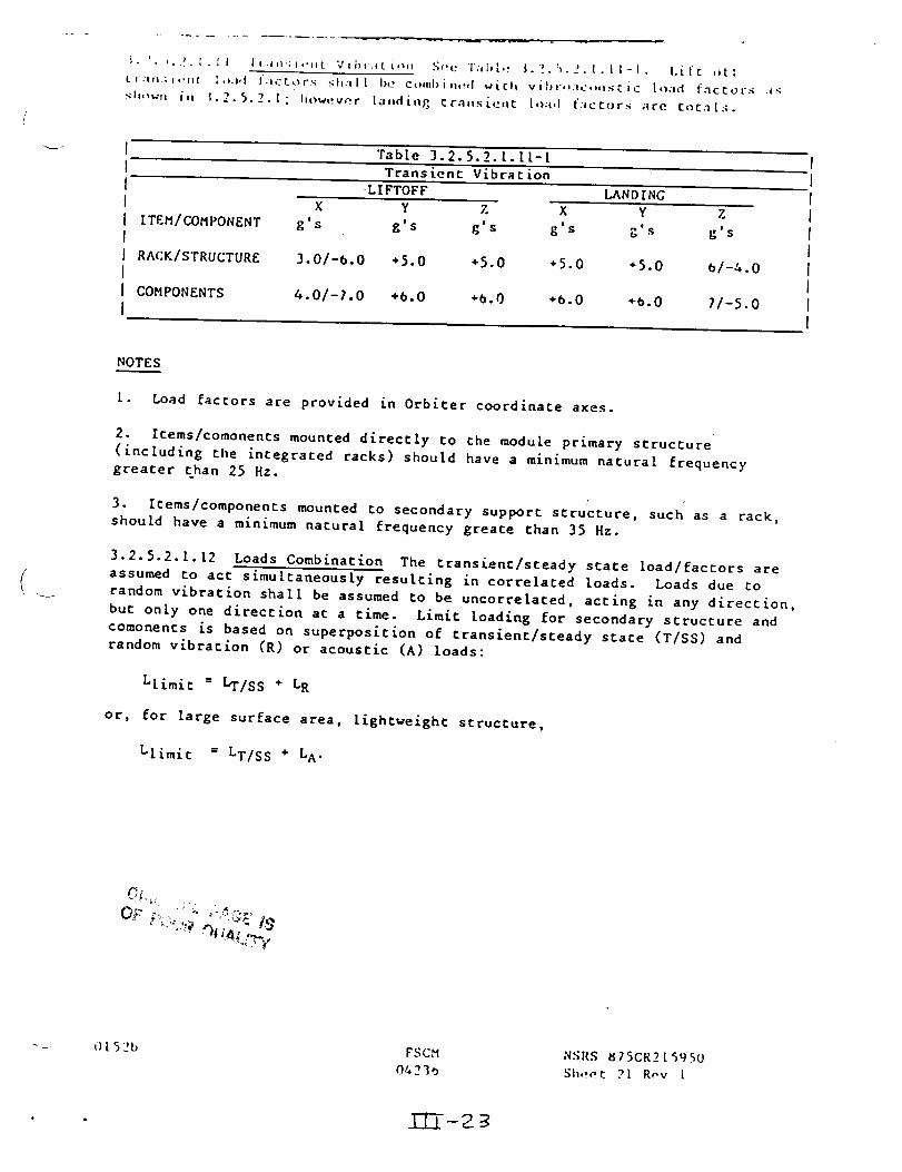
i. '. ,.2.:.l I I r.l,l:i,'Jll_ ?thr:ll.,.,_. S,r'e l'.Jh,[o" I.i._.:_,.!.l.|l-l. I.i.f[ ,_,1::
Lr.,.;i,.nl l,,.vl f.,c[ors sh.,ll I),.. c_..l_i._.l _ith vi,_r,,.,c,,-_ti¢ l_lad fnccot's ,,s
nl,,,w, i,, i.+_ ....5. + I" l,owt:vor la.cli.+ tr._ns[+;nt l,ta,l factors are [:neat:;.
Table 3.2.5.2.l.[I-I
Trans i.ent Vi.brar ion
L[FTOFF LANDING
X Y Z X Y Z
ITEM/COMPONENT g's g's g's g's g's g's
RACK/STRUCTURE 3.0/-6.0 +5.0 +5.0 ÷5.0 +5.0 b/-&.0
COMPONENTS 4.0/-7.0 +6.0 +6.0 ÷6.0 +b.O 7/-5.0
NOTES
I. Load factors are provided in Orbiter coocd[nar.e axes.
2. [cems/comonencs mounted directly ro Che module primary scrucr-ure
(_.ncluding the [ncegrared racks) should have a minimum natural frequency
grearer t_han 25 Hz.
3. [cems/componencs mounted Co secondary support, sr,rucr.ure, such as a rack,
should have a minimum nar,ura] frequency grear-e t:han 35 Hz.
3.2.5.2.[.[2 Loads Comb_nar,£on The r.ransienr,/sr-eady sCar,e toad/factors are
assumed co act simulr,aneousLy resul{:ing in correlar,ed loads. Loads due co
random vibrar,ion shall be assumed r,o be uncorre[ar,ed, acring in any direction,
bur- only one direct,ion at, a r-line. Limit, loading for secondary structure and
comonenr,s is based on superposiCion of transient/sr.eady st,ace (T/SS) and
random vibrat:ion (R) or acoustic (A) loads:
Llimir, = LT/SS + L R
or, for large surface area, lighr,weighC scrucr,ure,
L[imi c = LT/SS + LA.
Op
OLS2b NSRS 575CR215950
Sh,tc't 21 Roy [

Random Vibration Criteria
20 Hz20 - I00 Hz
100 - 200 Hz200 - 300 Hz
300 -1000 Hz
I000 -2000 Hz
2000 Hz
.006 g2/Hz3 dB/oc Cave
.03 g2/pz
-3 dB/oc Cave
.02 g2/Xz
-9 dB/oc rave
.0025 g2/Hz
Composite -5.3 grms
Random Vibration Load Factors
/ #
v
Figure 3.2.5.2.1.8-I Zone Cl+-l Common Module Cylinder
Wall Ring Frame/Longeron Junctions
0152b FSCM
04 236
NSRS 875CR215950
Sheet 22 Rev 1

Random Vtbcacton Crtterfa
20 liz .002 g2/Hz
20 - I00 Hz +5 dB/ocCave
100 - 600 Hz .03 g2/Hz600 -2000 Hz -6 dB/octave
2000 Hz .O028 g2/Hz
Composite = 5.34 g rms
Random v£brat£on Load Factors
f
Figure 3.2.5.2.1.8-2: Zone CH-2 CommoQ Hodul_ Cone SecC£ons
0152b FSCH
04236
NSRS 875CR215950
Sheet 23 Rev 1
III-Z

.... 7= - -- ....... ...r__
Table 3.2.5.2.2.6-L
Orblcer Cargo Bay CombLned Lifcoff/Boosc Acoustic Spectrum C1/3 Octave Band Sound Pressure Level (riB) -_..I
..Ce,nter Pcequency (Hz) Ref. 2 x 10⁻⁵___
20.0 118.0
25.0 120.0
31.5 122.0
40.0 124.0
50.0 125.5
63.0 127.080.0 ,- 128.0
I00.0 128.5
125.0 129.0
160.0 129.5200.0 129.0
250.0 129.0
315.0 128.5
400.0 127.5
500.0 125.0
630.0 123.0
800.0 121.0
1000.0 119.0
1250.0 117.5
1600.0 116.0
2000.0 114.0
2500.0 112.0
3150.0 110.54000.0 108.5
5000.0 106.5
6300.0 105.0
8000.0 103.0I0000.0 101.0
(Y4EIUtLL SPL 139.0
3.2.5.3 Orbital Operatlonal Envlror_encs The assembly shall meet the
iequlremencs specifled herein during and after exposure to the followim_
envl torment s.
3.2.5.3.1 Orbital Internal Environments
3.2.5.3.1.1 Temperature 18°C co 24°C (65°F Co 75°F) nominal:15.6°C to 29°C (60°F 1:o 85OF) 28 day degraded; 19.6°C to 32.2°C
_60°f Co 90°F) emergency; TI_ during emergency deconCaminaCion.
0152b FSCM
04 236
Ill-Z6
NSRS 875CR215950
Sheet 24 Rev i
ORIC._i'_;_,LPAGE IS
OF POOR QUALITY

<
T . ÷ o . _ _-u.-it
1.2.5.3.1.2 Pressure [00 to [(13 kPa ([4.3 to 14.9 psia) noml,_al; 1.3 x[0 -8 kPa (lO-[Otorr) during emergency decontamination.
3.2.5.3.1.3 llumldlty 4°C to I0°C dew_olnts (40°F to 50°F) nominal;
1.7°C to 32'}C dewpoints (35°F to 70°F) 28 clay degraded.
3.2.5.3.1.4 Rand_ Vibration 15-1000 @ .003 g/Hz1000-2000 @ 6 dB/oet.
3.2.5.3.1.5 Acoustics All areas for hearing conservation purposes shall not
exceed: LEQ I00 dB. Noise peaks, regadless of duratlon, cannot exceed 30 d8
over the baseline noise speclflcaclon.
3.2.5.3.1.6 Acceleration
3.2.5.3.1.7 Radiation TBD.
3.2.5.3.1.8 Transient Vlbratlon 0-20 Hz @ 0.26 g/0 peak.
3.2.5.3.1.9 Loads Combination See 3.2.5.3.1.12.
3.2.5.3.2 Orbital External Environments
3.2.5.3.2.1 Thermal Radiation
3.2.5.3.2.1.1 Solar Radiation 1371 +/-5W/m 2.
3.2.5.3.2.1.2 Earth Albedo 30%.
3.2.5.3...1.3 Earth Emitted Radiation 237 W/m 2.
3.2.5.3.2.1.4 Space Sink Temperature 3K (-270°C).
3.2.5.3.2.2 Ezternal Pressure
torr to 1 x I0 -_u torr).
2 X 10 -7 Co 1.3 x 10 -8 kPa (1.5 x 10 -9
3.2.5.3.2.3 Random Vibration TBD.
3.2.5.3.2.4 Acceleration TBD.
3.2.5.3.2.5 Particle Radiation
3.2.5.3.2.5.1 Ionosphere Plasma TBD.
3.2.5.3.2.5.2 ,Trapped Radiation T_.
3.2.5.3.2.5.3 Solar Cosmic Rays TBD.
3.2.5.3.2.5.4 Galactic Cosmic Ra_s TBD.
0152b _- .... _ _ FSCM
f_: ,_::(>(_ C_ i I -- 04 236
NSRS 875CR215950
Sheet 25 Rev 1
]IL-z7

1.2.5,L, _)rbit_t] Op,;ral:ioo i.:uvirot_neul:,_ T!-: _;l_ sl_l [ meet the reqtl[ccm_I1t._
._peciftc, I herein durtny) and after exposure to l:he folto_rtng environments.
3.2.5.4.1 Orbital Internal Enviror_ent._
3.2.5.4.1.I Temperature 18°C to 24° (65°F to 75°F) nominal; 15.6°C
to 29°C (60°F to 85°F) 28 day degraded; 19.6oc to 32.,2oc (60°F to
90°F) emergency; TBD during emergency decontamlnalon.
3.2.5.4.1.2 Pressure I00 to 013 kPa (14.5 to 14.9 psia) nominal; 1.3 x
10 -8 kPa (I0 -iO tort) during emergency decontamination.
3.2.5.4.1.3 llumldity 4°C to 10°C dewpoints (40°F to 50°F) nominal;1.7°C to 21°C dewpo£nts (35°F to 70°F) 28 day degraded.
3.2.5.4.1.4 Random Vibration 15-1000 @ .003 g2/Hz.1000-2000 @ -6 dE i oct.
The structure shall be capable of operaclng without structure damage under
these levels for 30 years.
3.2.5.4.1.5 Acoustics Component acoustic output cannot exceed
Leq (24) 70
Leq (24) 50m
dBA hearing conservation areas
dBA speech colmunlcatlon areas
Isolation provided if an impulsive sound exceed i0 dB above the baseline
specificatlon. No sound Bay exceed 30 dB above the baseline specification
levels regardless of duration.
If acceptance level acoustic or vibration is performed to a minlmu_ level
which exceeds 6 dB dow_ from the flight enveloped levels, the qualification
levels must exceed the accewptauce levels by 6 dB.
3.2.6 Transportability The RPC shall comply with NHB 6000.
3.3 ,Design and Construction
3.3.1 Parts, Materials, and Processes Parts, Baterlals, and processes shallbe selected and controlled in accordance with JSC 30233.
3.3.1.i Electrical Connections Connections between wires shall be by
positive, mechanically secure means such as crimped conductor splices,
connectors, or terminal boards.
3.3.2 Electromagnetic Interference (EMI) The RPC shall meet the F_MI
requtrmeuts for Class A2 equipment specified in MIL-ST_-461B.
3.3.2.1 Electrical Bonding Bonding shall be in accordance with HIL-B-5087.
0152b FSCH04236
NSRS 875CR215950
Sheet 26 Rev 1
C=,_'_'_; p,r-_,GEIS
OF POOR QUALITY

.. °
3.2.5 Environmental Requirements The folZoutng structU,L-al and environmentaldynamics cequlrements mus£ be met for all components mounted tnCecnally to
space scatlon modules.
I) C. Ernsberger, "Guidelines for space station modules strut,rural loads
analysis', NASA MSFC memo ED22-8S-40, 5 April 1986
2) NASA components analysis branch, "Deslgn and verlflcaClon guidelines for
vibrocousclc and transient environments', NASA TM--86538, March Z986.
3) NASA/MSFC space station projects office, "Space Station Program Definition
and Requirements" SS-SRD-0001, Sec. 30, 31 3uly 1986.
/
/
v
0152b FSCM
04236
NSRS 875CR215950
Sheet _t7 Rev 1
XII- 2q

3.3.2.5 Electroraasnetlc Envtro_Qent The RPC _IL_[I fuuction normally dnrin_,and after exposure co electroraagnetlc environment for class A2 equipment.
3.3.3 Nameplates and Product Markings
3.3.3.1 Identification Identification and marking of the RPC, Its
components, and parts shall be In accordance wlth MIL-STD-130. Nameplates
shall be used, where appllcable. Components _rlthln the RPC shall be
identified by a part number and serial number assigned by the Supplier.
Nameplates on the RPC shall Include at least the following infnrmatlon:
Manufacturer's part number
Approved nomenclature - (from I. i)
Controlling specification number - (from 1.2)
Manufacturer's name or trademark
Serial number - (Assigned by the Supplier as follows: _he serial
number shall consist of seven digits. The flrst three
digits may be any combination of letters and digits
provided the same combination is used for all part
numbers. The last four digits shall be numeric and
shall be assigned consecutively beginning wlth 0001.
Serial numbers shall be non-repetltlve.)
Contract number - (as specified In the P_ocurement Agreement)
3.3.3.1.1 Test Particles All Development RPC shall ibe permanently marked"Not for Operational Use - Development Only'. All Operational type RPC which
are subjected to quallflcatlon testing shall be permanently marked "Not for
Operational Use - Qualification Only".
3.3.3.1.2 Equipment Labels Labels shall be engraved or chemically etched on
the TED surface, or engraved staked metal places may be used. Paper decals
and rubber scamping shall not be used. Idenclflcatlou sleeving may be used on
electrical cables.
3.3.3.2 Electrical and Electronic Reference Designations ElecCrlcal and
eleccronlc reference deslguaclons for external electrical connectors shall be
affixed co the RPC in accordance with the cequlrements of ANSI Y32.16 as
modified by the Procurement Agreement.
3.3.4 Workmanship The gPC shall be fabricated and finished In a thoroughlyworkmanlike manner. Particular attention shall be given to freedom from
blemishes, defects, burrs, and sharp edges; accuracy of dimensions; radii of
fillets; marking of parts; thoroughness of cleaning; quality of brazins,welding, riveting, painting and wiring; alignment of parts; and tightness and
torqulng of fasteners.
3.3.5 Interchangeablllty and Replaceablllcy Assemblies, components, and
parts having identical part numbers shall, meet the requirements for an
Interchangeable item as defined in 6.1.4 herein. Where interchangeabilicy Is
not practicable, the requirements for a replacement Item as defined in 6.1.5
herein shall apply.
(
0152b FSCM
04236
_[l-gO
NSRS 87 5CR215950Sheet 28 Rev 1
O_,c,_,v_--.'-',-:" _-_ ISOF POOR QUALITY
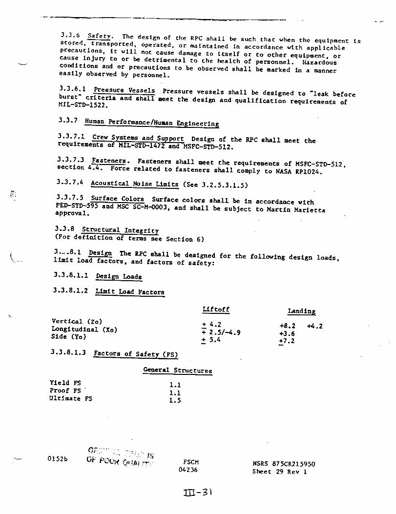
3.3.6 Safety. The deslgn of else RPC shall be such chat when the equlpment Ls
scored, transported, operated, or maintained In accordance vlch applicable
precauclons, it will noc cause damage co Itself or Co ocher equipment, or
cause Injury co or be detrimental co rhe health of personnel. Hazardous
conditions and or precautions co be observed shall be marked in a manner
easily observed by personnel.
3.3.6.1 Pressure Vessels Pressure vessels shall be designed to "leak before
burst" cr£cet-la and shall meet the design and qualification requirements ofMIL-STD-1522.
3.3.7 Human Performance/Human En_Ineerln _
3.3.7.1 Crew Systems and Support Design of the RPC shall meet therequirements of MIL-STD-1472 and MSFC-STD-512.
3.3.7.3 Fasteners. Fasteners shall meet the requirements of MSFC-STD-512,
section &.4. Force related co fasteners shall comply to NASA RPI024.
3.3.7._ Acoustical Noise Limits (See 3.2.5.3.1.5)
3.3.7.5 Surface Colors Surface colors shall be in accordance with
FED-STD-595 and MSC SC-M-O003, and shall be subject to Martin Marletca
approval.
3.3.8 Structural Inte_rity(For definition of terms see Sect£on 6)
3.-.8.1 Design The RPC shall be designed for the following design loads,
limit load factors, and factors of safety:
3.3.8.1.1 Design Loads
3.3.8.1.2 Limit Load Factors
L£ftoff Landin_
Vertical (Zo) + 4.2 +8.2 4_.2
Longitudinal (Xo) _ 2.5/-_.9 +3.6
Side (Yo) + 5.4 +7.2
3.3.8.1.3 Factors of Safetg.(FS)
General Structures
Yield FS i.I
Proof FS I.I
Ultimate FS 1.5
0152b FSCM
04236
NSRS 875CR215950
Sheet 29 Rev 1

].].8.'2 ".1.1rt_tu.q of Safety ,\it ._trucCur,_.q s!,ntt me,:t [:lie r_:qutreme,q[ for ;:_ro
or po._lclve m,_rglns of safety cnlculated In accordance with SS-SRD-O00! £e(:.3.0, i>rocedu_res.
3.3.8.3 Allowable Stresses The RPC shall he deslgned for material allowable
stresses obtained as follows:
a. MIL-HDBK-5
b. Approprlate tests or sources approved by Martln Marietta.
The effects of temperature shall he accounted for In defining allowable
material strength and properties.
3.3.8.4 Allowable Deflections The deflections of the RPC shall be designed
such that there are no permanent defocmatio_s during normal operations.
3.3.9 Posltlve-locking Devlces Positlve-locklng screw-type hardware shall
be used on the RPC where practicable. Safety wiring shall he In accordance
with MS33540.
3.3.11 Dlmensionln_ and Tolerancin_ For figures hereln dlmenslons are in
millimeters. Dimensioning and toleranclng are per ANSI Y14.5. Unless
otherwise specified, tolerances on mechanical features shall be as specifiedbelow:
/
Linear X.XX + .25
Angles + 30 Minutes X.X • .75X 3 +i
X 3 +2.5
3.3.12 Product Cleanliness Surfaces of hardware shall be free of all visible
contaminatlon, such as fingerprints, particles, corrosion products, metal
chips, scale, oli, grease, preservatives, adhesives and any other foreign
matter. Vlsual inspection shall be accomplished without magnification under
good lighting conditions. Wipe tests, waterbreak tests, ultraviolet light
inspection, special lights and mirrors, are considered aids to visual
inspection.
Cleaned hardware shall be maintained In a clean area to prevent
recontamInatlou until such time that It is packaged In clean double bags for
shipment.
External and internal surfaces shall meet the visually clean requirementsdescribed above. [Internal surfaces of fluid systems, I.e. valves, orifices,
etc. are to be cleaned and verified to the Individual requirements detafled bythe deslL_n.]
The hardware shall be fabricated from materials that meet the material
constraints of SP-R-0022A and cleaning procedures adequate to insure the
removal of any process consumables used in the manufacture of the hardware
shall be established.
0152b FSCM
04236
311-3Z
NSRS 875CR215950
Sheet 30 Rev I
OF POOR QUALITY
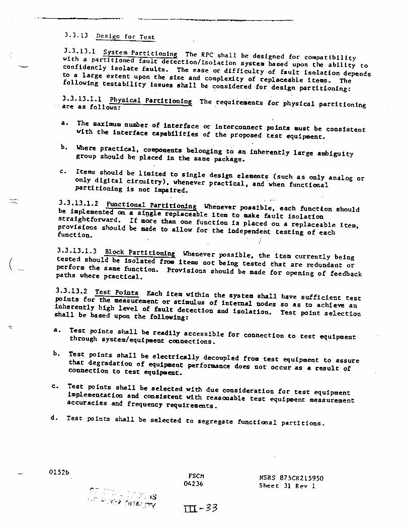
3.3. t3 Destgn for Test
3.3.13.1 System Partltlonln_ The RPC shall be designed for compatibility
wlch a partitioned fault detectlon/lsolarlon system based upon the ab£1lty to
confldencly isolate faults. The ease or difficulty of fault lsolaclon depends
to a large extent upon the size and complexity of replaceable items. The
following testability issues shall be considered for design parClcLoning:
3.3.13.1.1 Physical ParCltlonlng The .requlremenCs _or physlcal partitioningare as follows:
a. The maximum number of Interface or interconnect points must be consistent
WlCh the interface capabilities of the proposed rest equipment.
b. _here pracclcal, components belonging cO an inherently large ambiguity
group should be placed in the same package.
c. teems should be IImlced Co single design elements (such as only analog or
only digital circuitry), whenever practical, andwhen functional
partitioning is not impaired.
3.3.13.1.2 Functional PartlCion/n_ Whenever possible, each function shouldbe implemented on a sl.ngle replaceable item to make fault isolation
stralghcforward. If mote than one funcClon is place d on a replaceable item,
provisions should be made to allow for the Independehc cesclng of each
func t i on. /
3.3.13.1.3 Block Partltlonln_ Whenever possible, the Item currently being
tested should be isolated from items not being tested chat are redundant or
perform the same function. Provisions should be made for opening of feedback
paths where p-tactical.
3.3.13.2 Test Points Each item wifl_in the system shall have su£flclent test
points for the measurement or stimulus of internal nodes so as to achie_ an
inherently high level of fault detection and isolation. Test point selection
shall be based upon the following:
a. Test poluts shall be readily accessible for connection to test equipment
through syscem/equlpment connections.
b$ Test points shall be electrically decoupled from cesC equipment Co assure
that degradation of equipment performance does not occur as a result of
connection to test equipment.
Co Test points shall be selected with due consideration for test equipment
£mplementatic_ and consistent with reasonable test equipment measurement
accuracies and frequency requirements.
d. Test points shall be selected Co segregate funcclonal partitions.
0152b FSCM
04236
II-33
NSRS 875CR215950
Sheet 31 Rev 1
eo Test polncs shall be chosen such that hlgh voltage and current
measurements are conslscenc wlch safety cequlremenCs and are physLcally
isolated from low logic level signals.
f. Test point measurements shall relate Co a common equipment ground.
3.3.13.6.1 Concurrent Concurrent (continuous) fault detection techniques
(utilizing hardware redundancy) are used for monitoring chose functions which
are mission critical or affect safety and where protection must be provided
against the propagation of errors through the system.
3.3.13.6.2 Periodic Periodic testing Is used for monitoring those functionswhich provide backup or standby capabillcles or are hoe =/_ston crlttcal.
3.3.13.6.3 On-demand On-demand cesclng 1_ .used for monltoring those
functions vhlch require operator 'interaction, sensor simulation, or which are
noC easily, safely, or cost-effectively initiated automatically.
3.3.13.6.4 Malncenance Capability For each level of maintenance,
Bullt-ln-cest (BIT)/ off-llne automatic test_and manual test capabilities
shall be integrated to provide a consistent and complete maintenancecapability. The degree of test automation shall be consistent with the
proposed personnel skill levels and corrective and preventive malnCenancerequirementS. _
/
3.4 Supplier Documentation The Supplier shall furnish documentation in
accordance wlth the Procurement Agreement.
0152b FSCH
04236
.Z!-3q
NSRS 875CR215950
Sheet 32 Rev 1
OF POOR QUALITY

(
,;. u L_IIAI. ; TY "'"" .... [ SA._ ._,;RAN(.E PROV [ c.);',,'.q
/..[ General This section describes the requirements for the verification of
the Section 3 requirements during design and fabrication, and acceptance andqualificarton test programs.
4.1.I Responsibility for Verification The Supplier slhall perform all or any
part of the verlflcacgou activities of thls drawing when so ¢equlced by Martin
Marietta in the Procurement Agreement. In the event Martin Marietta elects to
perform any part or all of the tests identified, or have them performed by
others, the Supplier shall either write the test procedures or comment and
mutually agree upon the test procedures. The dlrectlon for either originating
or approving these test procedures will be in the Procurement Agreement. The
Supplier shall either provide technleal dlrectlon or shall have represencatlon
present for any part or all of the tests when required by the Procurement
Agreement. The Supplier may monitor these tasks at his option and shall
accept _he results of any tests which have been performed In accordance with
procedures approved by the Supplier. The Supplier shall accept the results
whether Martln Marletta or the Supplier contracts fo¢ the testing.._
4.1.2 Quality Assurance Requirements A Quality Assurance Program shall be
conducted at the suppller's facilities In accordance with the quality
assurance requirements defl_ed in the Procurement Agreement.
_.i.3 Notification of Tests The Martin Marietta buyer shall be notified i0
days prior co the time tests are to be conducted. In addition, Martin
Marietta reserves the right to witness all tests.
4.1.4 Test Program Controls The Suppller shall incorporate the following
test program controls.
4.1.4.1 Facilities and Equipment Facility and equipment requirements shall
be as specified in M-67-_5 Sections _ and 5. In addition, still and video
photographs shall be required to the extent defined in the Procurement
Agreement.
_.i._.2 Non-conformance Reporting Non-conformance reporting shall be asspecified in M-67-45 Seetlon 9..
4.1.4.3 Test Documentation Test documentation shall be pre_ared inaccordance wlth M-67...,45 Sectlon 6.
4.1.4.4 Test Methods and Conditions Implementation of the test requirementsherein shall be in accordance with the detailed test methods and conditions
specified in M-67-45. Requests for any deviations from M-67-45 deemed
necessary shall be approved by Martin Marietta. The test procedure shall be
prepared by the Supplier and approved by Martin Marietta in writing prior to
the start of any tests.
0152b
OE _ _c__ Qu_Ltyy
FSCH
04236
ORIGINAL PAGE ISOF POOR QUALITY
NSRS 875CR215950Sheet 33 Rev I
_- gS"

4.2 ,._H', icy Conforn_lnce Verification - The r{-luir_tm.'nt.q n[ Section 3 I.,rei;_
:;h.tll he verified by combination nf Inspection, demonstration, analysts and
t,'_cinp,. Table [ defines the verification requirements that shall be used tosatisfy the cequtrements specified In Section 3. In addition, functional and{_..rformance tests shall be conducted In the testing sequence (Tables [[ and
£II) to evaluate the effects of testing.
4.2.1 VerlflcaCiOn Methods The following methods shall be used:
al Inspecclon InspectI,_. [_ a ,aetlLod of verification constsClng of
Investigation, without the use of special laboratory appliances orprocedures, ¢o determine compliance wtch requirements. Inspection Is
nondestructive and Includes (but is not li=ited to) visual examination,
simple physical manlpu!atlon, gauging, and measurement.
be
C=
Demonstration Demonstratlon Is a method of verification that is limited
to readily observable functional operation to determine compliance with
requirements. This method may not require the use of special equlpment or
sophl st£caced Inst rumentation.
Analysts Analysis ls a method of verlficat£on caking the form of the
processing of accumulated results and conclusions, inCencLed to provide
proof tha¢ ver£fEcat£on of a requirement or requirements has been
accomplished. The analytlcal results may be based on engLneerlng study,
compilation or incerpretaClou of existing Informatlon, similarity to
previously verified requlrements, or derived fro= lower level
exam_natlons, tests, demonstrations, or analyses. Submittal of analysls
data shall be as required in the Procure=eriC Agreement.
dq, Tes.._t Test ts a method of verlficat£on Chat employs technlcal means
Including (but not limited to) the evaluation of functional
characterlsc1cs by use of special equipment or Instrumentaclon, slmulatlon
cechn(ques, and the application of established principles and procedures
Co determine compliance with requirements.
4.2.1.1 Qualification by Similarity When qualification by similarity to a
previously qualified Item is proposed by the supplier such quallflcatlons
shall be subject ¢o Martin MarletCa approval and shall meet the requirements
specified in the Procurement Agreement.
4.2.2 Test Cate6or 7 Definitions
a= Development Tests Development testing is a test or series of testsconducced co evaluate and confirm the feaslbillty of the design approach
and provide confidence £n the ability of the hardware to meet
quallflcaclon and acceptance requlremencs. Tests shall be performed
primarily to acquire data to support the design and development process.
The development hardware should be representative of, but noc necessarily
Identlcal to, production hardware.
0152b FSCM
04236
NSR S 875CR215950
Sheet 3_ Rev ]
OF_{g!;_AL PP_GE IS
OF POOR QUALITY

Accept.ince Tc..qts Acceptance tests ,are the requited fo.'_m;il tests condo:tied
to demonstrate acceptahtltty of an Item for delivery. Acceptance testsmay consist of performance, functional and acceptance lev_l envtronmentat
tests. This testing is conducted to detect manufacturing flaws and
defects that may not be detected by other Inspection techniques.
Acceptance tests shall he performed on each production and qualificationun£t.
Co Qualfficatlon Tests Qualification (certification) tests are focmal
contractual demonstrations that the design, Implementation, and
manufacturlng methods have resulted in hardware conforming ¢o
specLflcatlon requirements. The qualification tests are usually conducted
at levels and for durations that assure the production items will perform
satls_actorily in t_ use environments with sufflcler¢ margin.
QuaiLElcatlon hardwarels fabricated to production equipment drawings
using specified materials and production methods and shall be
representative of deliverable production hardware. Qualification testing
shall be conducted as part of the total verification process of the design
and fabrlcatlon compliance.
4.2.3 Test Type
a. Performance Test The operating test that verifies all functions and
circuits are operating as required by tie unit design specification. All
performance tests may be conducted at laboratory ambient conditions.Performance tests shall be conducted at the sta_ and concl_slon of the
acceptance and quaiLflcation test program.
b. Funet/onal Test The operating test that is no_aally a subset of the
performance test requiring minimal operation to verify proper operation of
the unit under test. These tests shall be conducted before, during, and
after each envlronmental test as defined herein. Functional tests shall
be perfomed at laboratory ambient conditions or the environmental
exposure conditions when specified.
4.3 Test Requirements
4.3.1 Development Tests Development testing shall be performed only when
specified In the procurement agreement. Any development testing that is not
specLfled In the Procurement Agceement shall be the sole responslblllty of the
Supplier. The results of such tests will not _,_ accepted by Martin Harlecca
for design verification purposes. The results of any development tests
specified in the Procurement Agreement shall be documented and submltted co
r'5-;,_::,:_L :'"_:_.e1S
O152b FSCH
04236
NSRS 87 5CR215950
Sheet 35 Rev 1
.lit-37
!2
";._rtlu :.1;_r_,.tt_i for Engln,,,'rlng ¢oneurr,:uce. In the ,_vent such :;perilLed
,!evelol_nent test results are Intended to he used as part of the verification
process, the test sl_ll be predeclared and the test controls specified In theProcurement ARreement shall he applied.
4.3.2 .Ac..ceptance Tests - Acceptance tests as spectfled in Tables I and IIshall be conducted on each production unit and each qualification test unit.
Performance and acceptance testing of items requiring computer control shall
be performed with validated computer control software or a Martin Marlettaapproved simulatlon thereof.: Operation with co=purer control acceptable to
Martin Marletta shall be a c0ndlclon of acceptance testing.
4.3.2.1 Performance Tests Tests shall be conducted to verify or support
verif/cation with Paragraphs 3.2, 3.2.6, and 3.3. The sequence of testing
shall be as listed in Table II In accordance with paragraph 4.2.3, herein.
4.3.2.2 FuncCIonal Tests Functional tests shall be perfor_d to demonstrate
compliance with paragraphs 3.2 and 3.3. The order of cesclng the functional
parameters shall be as listed in Table II. These tests shall be conductedbefore, [during], and after each envlrorusental test as defined in 4.3.2.3 and
subpa rag raphs... . ...
,%
4.3.2.3 Environmental Tests Performance test, as deflned in 4.2:3 shall be
conducted Prior to the £1rst env_ron=encal eest and after completi0n of allenvironmental tests. [PD _rlter; List all the acceptance envlrouaeutal tests
that are required to be performed In sequence, i.e., examples below: Ifsequence is a problem, consult the System Test Group.'] Tests shall be
performed in the sequence shown tn Table If.
4.3.2.3.1 Acceptance Thermal Vacuum Test Components (subassemblles)
identified as sensitive to a vacuum environment shall be tested in accordance
with Paragraph 8.3 of M-67-45, wlth the temperature llmlts and durations notedbelow.
4.3.2.3.1.I Acceptance Temperature Limits The 10°C quallficatlon margin
shall be subtracted from the maxlmum and mlnimum quallflca_ion limits defined
in para. 3.2.5.1.1 herein..
4.3.2.3.1.2 Acceptance Test Duration - A =£ni=um of 8 thermal vacuum cycles
are requited. The dwell times at maximum ard minimum temperatures shall be a
minimum of 2 hours after temperature stabilization except Chat a 12 hour dwell
after Cempecature stabillzat£on with a cold start shall be requlced in the
first cycle and a 12 hour hot dwell after temperature stabilization wlth a hot
start shall be required in the last cycle.
4.3.2.3.1.3 Stabilization of Test Temperature The test uD/t a.d
baseplace/chamber temperatures shall be stabilized prior to the star_ of the
test. Temperature stabilization shall be considered established when the
readings of all central temperature sensing devices are within 1.7°C (3°F)
of the specified temperature for 3 consecutlve readings taken 5 minutes
/
O152b FSCM
O4 236
I11- 8
NSRS 875CR215950
.Sheet 36 Rev I
OF POOR QUALITY

L
•_pqrt. ._',,r tL.st -.LL_ [._r,,.er tlL_,_ [3._ k_. (30 i)ou.,l:;), ._tabillz;tc[on ._lkall i_co_s[,lered established when .3 consecutive reJitl[ngs t:lken 5 minutes apart are
within 2.R')C (._°F) of the speclf[,:d temperature. During thermal cycling,
chamber temperatures shall be measured u._tn_ a minimum of two temperature
senslnR devices located In the free alrflow, within 12.7 cm of opposite sldes
of the test unit. Baseplate temperatures shall be measured using a mlnlmum of
2 temperature sensing devices located at opposite sides of the thermal
Interface. Temperature of the test unit shall be measured using a minimum of
2 temperature sensing devices located as near as possible co the mass center
of the test unlt. During thermal vacuum testing, temperature sensing devices
stroll be placed on all chamber walls and doors as well as the baseplace co
verify stabIllzaclon. Application of temperature sCabillzatlon shall be in
accordance wlth Paragraph 8.3 (thermal vacuum) and 8.4 (thermal cycling) ofM-67-45.
4.3.2.3.2 Acceptance Thermal Cycle Test The RPC shall be tested in
accordance with Paragraph 8.4 of M-62-45 wlch the temperature limit and
duration exception noted below. Functional testing shall be limited co a pre
and post test funcCloual test plus periodic abbreviated funcclonal tests
during the _hermal cycling test to verify performance.
4.3.2.3.2.1 Temperature Limits The 10°C qualification margin shall be
subtracted from the maxlmum and minimum qualification limits defined in
para.3.2.5.1.1 herein. The stabilization requirements of paragraph
4.3.2.3.1.3 also apply co this test. /
4.3.2.3.2.2 Test Duration A minimum of 8 thermal cycles are required on
components not thermal vacuum tested. For component level acceptance tests,
thermal vacuum or thermal cycle tests are required, but noc both. For thermal
cycle tests the dwell times at maxlmum and minimum temperatures shall be a
minimum of 2 hours after temperature stabilization except that a 12 hour cold
dwell after temperature stabilization with a cold start shall be requlred in
the first cycle and a 12 hour hot dwell after temperature stabilization with a
hot start shall be required in the last cycle.
4.3.2.3.4 Acceptance Random Vibration The RPC shall be tested in accordancewith Paragraph 8.2_I of M-67-45 except Chat the test levels shall he those
specified by Martin MarletCa. The duration of the acceptance random vibration
test shall consist of a 1.0 mlnute exposure in each of the three orChogonal
axis. A functional test shall be performed prior to and after completlon of
cestlng in all three axes. Power spec=r_l density plots of the Input
acceleratlon and cross-axes response shall be provided.
4.3.2.3.5 Acceptance Pressure/Leak Test The RPC shall be acceptance testedfor pressure and leakage in accordance with the respective Paragraphs 8.12 and8.11 of M-67-45. Batteries shall be tested at the cell level only.
4.3.2.3.6 Acceptance Weight Measurement After completion of the acceptancelevel environmental tests, a weight measurement test shall be performed on the
unit. The weight of the unlt shall be measured In a condition nearly
equivalent co the launch manifest configuration. The equipment status at the
clme of measurement shall be logged and shall become a part of the records and
welghC report.
0152b FSCH
0_236
EiZ.-3ct
NSRS 875CR215950
Sheet 37 Rev I
t-,,_;,',r_,."_, PAGE iS
OF _';;..::i"i',_r_ll_ tTY

4.3.2.3.7 Acceptance Run-ln-Test Hechanlcal and eLectromechantcal components
and subassemblLes shall be mechantcaLiy cycled in accordance with Paragraph8.37 of H-67-_5.
4.3.3 Quallficatlon Tests - Quallflcatlon tests shall be performed on each
test unit as specified in Tables I and III. Test artZcles shall be the same
configuration as the production hardware. Successful completion of
inspections and acceptance tests of Section 4 shall he a pce requls£ce to each
test unit entering quallflcaClon test.
4.3.3.1 Performance Tests The same test conditions specified in paragraph
4.3.2.1 shall apply using the test sequence listed In Table III. With Martin
Marietta approval, the fZnal acceptance performance test may serve as the
pre-quallflcatlon performance test.
4.3.3.2 Functional Tests Functional cesta shall be performed to demonstrate
compliance wlth paragraphs 3.2.1, and 3.3.2. The order of testing the
functional parameters shall be as l[s.ted In Tables I and III. These tests
shall be conducted before, [durLng], and after each environmental test as
defined in 4.3.3.3 and subparagraphs.
4.3.3.3 Environmental tests Environmental tesCs shall be performed In the
sequence shown in Table III.
/4.3.3.3.1 Quallficaclon Thermal Vacuum Test Components Identified as
sensitive Co a vacuum environment shall be tested in' accordance with Paragraph
8.3 of M-67-45. With the temperature limits and durations noted below.
4.3.3.3.1.1 Qualification Test Temperature Limits Test temperature limitsare determined by the type of thermal control system employed.
a. Passive Thermal Control The maximum predicted plus 21°C and the mZnlmum
predicted minus 21°C.
b. Active Thermal Control (applicable to coldplate mounted items) Themaximum predicted plus II°C and the minimum predicted minus lO°C.
4.3.3.3.1.2 _ualiflcatlon Test DuracZons A minimum of 8 thermal vacuumcycles are required on vacuum senslt£ve components. The dwell times at
maximum and m£,,_uum temperatures shall be a minimum of 2 hours after
temperature stabilization except that a 12 hour cold dwell after temperature
stabilization with a cold start shall be required in the first cycle and a 12
hour hot dwell after temperature scabZl_zatton with a hot start shall be
required in the last cycle.
/
0152b FSCM
04236
EIX.-40
NSRS 875CR215950
Sheet 38 Rev I
ORIC3iNAL PAGE IS
OF POOR QUALITY

4.3.3.3.l.3 Stabilization of Qualification Test Temperature The test unitand haseplate/chamber temperature shall be stahtllzed prior to the start ofthe test. Temperature stahitlzatton shall be considered established when the
readings of all central temperature sensing devices are within 1.7°C (3°F)
of the specified temperature for 3 consecutive readings taken 5 minutes
apart. For test units larger than 13.6 kg (30 pounds), stabilization shall beconsidered established when 3 consecutive readings taken 5 minutes apart are
within 2.8°C (5°F) of the specified temperature. During thermal cycling,
chamber temperatures shall be measured using a minimum of two temperaturesensing devices iocaced In the free airflow, within 12.7 cm of opposite sides
of the test unit. Baseplate temperatures shall be measured using a minimum of
2 temperature sensing devices located at opposite sides of the thermal
interface. Temperature of the test unit shall be measured using a minimum of
2 temperature sensing devices located as :near as possible to the mass center
of the test unit. During thermal vacuum testing,, temperature sensing devicesshall be placed on all chamber walls and doors as well as the baseplate to
verify stabilization. Application of temperature stabilization shall be in
accordance wlth Paragraph 8.3 (thermal vacuum) and 8.4 (thermal cycling) ofM-6 7-4 5. _
4.3.3.3.2 Qualification Thermal Cycle Test Components shall be tested in
accordance wlth Paragraph 8.4 of M-67-45 with the temperature limits and
durations noted below. Periodic abbreviated functional testing shall be
performed during thermal cycling test to verify performance.!
4.3.3.3.2.1 Oualiflcatlon Temperature Limits Same as for thermal vacuum in
Paragraph 4.3.3.3.1.1 herein.
4.3.3.3.2.2 Qualification Test Durations
4.3.3.3.2.2.1 Vacuum Sensitive Components Components which have been thermal
vacuum tested will not be thermal cycled.
4.3.3.3.2.2.2 Components Hot Vacuum Sensitive Components that are notthermal vacuum tested will be exposed to 8 thermal cycles. The dwell times at
maximum and minimum temperatures shall be a minimum of 2 hours after
temperature stablllzatton except that a 12 hour cold dwell after temperature
stabilization with a cold start shall be required in the first cycle and a 12
hour hot dwell after temperature s_ablllzatlon with a hot start shall be
required in the last cycle.
4.3.3.3.3 Qualification Random Vibration Components (subassemblies) shall be
tested in accordance with Paragraph 8.21 of M-67-45. The test levels shall be
specified by Martin Marietta. The duration of the random vibration test shall
consist of 3.0 minute exposure In each of the three orthogonal axis. During
the test, the components shall be attached co a rigid test fixture
representative of its mounting. A functional test shall be performed prior to
and after completion of testing in all three axes. Power spectral density
plots of the input acceleration and cross-axls response shall be provided.
0152b FSCM
04236
33=L-
NSRS fI75CR215950
Sheet 39 Rev I
CF P;..-'.'©:_Q',._ALIT'Y

4.3.3.3.4 Qualiftcacton Accelratlon Test
4.3.3.3.5 QualtfLcation Pressure/Leak Test As applicable, components shall
be tested in accordance with Paragraphs 8.12 and 8.11 of M-67-_5 for pressure _._J
and leak tests respectively. Batteries shall be tested at the cell level only.
4.3.3.3.6 Qualification KMC Test The electromagnetic interference :
characteristics (emission and susceptibility) of the components
(subassemblies) shall be tested in accordaace with Paragcaph 8.35 0f M-67-_5.
• / _ - t ? " -L ;
4.3.3.3.7 Life Test Life testlng shall-be as specified in Paragraph 8.36 of
4.3.3.3.8 .Toxlclty Tests The RPC shall be tested as specified In TBS.
4.3#3.3.9 Audible Noise Measurements The RPC shall be tested for emitted
audible noise as specified in TBS. .,
4.3.4 Certification The hardware represented by this document shall be
certified relati_ to the Section 3.0 requirements herein. The supplier shall
provide documentation to support certification as specified' in the" Procurement
Agreement.
0152b FSCM
0_236
NSRS 875CR215950
Sheet 40 Rev 1

......mm,_, _ ...... 4-- _ -
5.0 PREPARATION FOR D£1.IVERY
5.1 General Preparaclon for delivery shall be _n accordance wlch the terms
of the Procurement Agreement.
.5.2 Markln_ For Shipment Marking for shlpment shall be In accordance withMIL-STD-129.
l
(
ORIGI[_!AL PAGE IS
OF POOR QUALITY
0152b FSCM
04236
NSRS 875CR215950
Sheet 41 Rev 1
IIl-

,_.O rh JTiLq
6.[ Definitions
6.1.t SupplierAgreement.
The Supplier [s the organization a_arded the Procurement
6.1.2 Procurin_ A_ency The Procuring Agency is NarCln Marietta Denver
Aerospace or as designated In the Procurement Agreement.
6.1.3 Procurement A_reement The Procurement Agreement is the written
purchase order, subcontract, or other Instmament of purchase or intent to
purchase, as agreed by Martin Marietta and the Supplier, including any written
negocia_ed changes or revisions thereto. The Procurement Agreement will
supplement the following paragraphs of this Drawing.
2.1
3.3.3 .I
3.3.3.2
3.4
4.1.1
4.1.2
4.1.4 .i
4.2.1.c
4.2.1.i
4.3.1
5.i
Applicable Document Revision Letter or DaCeIdentification
E1ectrLcal and electronic reference des_nations
Supplier Doeumentatlon
Responsibility for Tests
Quality Assurance Requirements
Facilities and Equipment
Analysis
Qualification by Similarity
Development Tests
Preparation for Delivery
6.1.4 Interchangeable Items When two or more items possess such functional
and physical characteristics as to be equivalent in performance and durability
and are capable of being exchanged one for the other without alteration of the
items themselves or of adjoining items except for adjustment, and without
selectlon for fit or performance, the items are interchangeable.
Interchangeable items are manufactured with the aid of controlled tooling and
require only the application of attaching means for their installation.
6.1.5 Replaceable Item An item which is functio**ally interchangeable with
another item, but which differs physically from the original part in that the
installation of the replaceable part requires operations such as drilling,
reaming, cutting, filing, shimming, etc., in addltton co the normal
appllca_ions and methods of attachment, is known as a replaceable item.
Replaceable i_ems are manufactured with the ald of controlled tooling and
require al_eratlon of the items in addition to normal methods of attachment.
6.1.6 Part One piece or two or more pieces Joined together which are not
normally subject to disassemblywithout destruction of designed use.
6.1.7 Component A combination of parts, devices and structures, usually
self-concalned, which performs a distinctive function in the operation of the
overall equipment, e.g., a "black box'.
/
0152b FSCM
04236
NSRS 875CR215950
Sheet 42 Rev I

_ -v.--.
6.1.R OperatIng Failure Rate Tl.z operating failure rate represents a
mathematical combination of failure rates associa_ed with a part's failure
modes which might occur In an operational sequence. The operatin E failure
rate is analytically determined.
6.1.9 Launch Hanifest Configuration TBS.
6.1.10 Limit Factors A load factor is a raClo by which the mass of an
assembly or an external load, is multlplied in order to obtain the limit load
action on the structure or a part thereof.J.
6.1.11 Limit' Load _ Limit load is the .maximum load or force expected In
service for a particular design coQdltio, and Includes the effects of dyuamlcs.
6.1.12 Yield Load The yleld load Is equal to. the llmlt load multlplled by
the yield factor of 'safety. The yield load is that load at or below which
general yielding of the structure must not occur.
6.1.13 Ultimate Load The ultimate load is equal'to the llmlt load multlplled
by the ultimate factor of safety. Rupture or complete structural collapse
shall not occur at or below ultimate load.
6.1.14 Proof Load The proof load Is equal to _he'li_lt load multiplied by
the proof safety factor. The proof load shall be of sufficient magnitude to
assure that the part can sustain limit load conditions, as required,throughout its service llfe. • l
6.1.15 Factor of Safety The factor of safety £s an arbitrary factor Intendedto account for slight variation from item to Item in fabrlcatlcm quality and
details, Internal load dlstrlbutlou wlthln the structure and possible
degradation In s_rength. ;'
6.1.15.1 Yield Factor of Safety The yleld factor of safety is the ratio of
_.eld to limit load. '
6.1.15.2 Ultimate Factor of Safety The ultimate factor of safety is theratio of ultlma_e load to llmlt load.
6.1.15.3 Proof Factor of Safetz The proof factor of safe_y is the ratio of
proof load to limit load.
6.1.16 Yield Strength Yield strength (stress) is the stress at which a
structural material exhlb£ns a 0.2 percent permanent deformation.
6.1.17 Ultlmate Strength Ultimate strength (stress) Is the maximum stresswhich a structural material exhibits prior to material rupture or other
failure mechanism of the material.
6.1.18 Orbital Replaceable Uait (ORU) Orbital Replaceable ualr.s are hardwareelements whose design enables Remote Au_omatlc fault detectlon/fault
isolation, removal, replacement and checkout by organizational maintenance.
0152b FSCH
04236
NSRS 875CR215950
Sheet 43 Rev 1
OR:_INAL pAGE ISGF pC,OR QUAL_Y

6.1.19 Circuit Isolation The tncecctrcuit Isolation requirement appliesbetween functional electrical ctccutcs which interface between two
equipments. The requfremenc applies over the operating frequency range of the (Ci rCu J. tS. \
6.1.20 Electrical Circult Reference Connection For the purpose of the
circuit to reference connection requirement, an electrical clrcu£t ts defined
as a functlonal electrical connection between two equlPments. :
6.1.21 Electrical Reference All conductive parts Which are not part of
functional electrical circuits are bonded together to form an electrical
reference. The electrical ,reference is not used for the conduction of
functional current, except for ,vehicle _I Ightlng.:_
6.2 Abbreviations and Acronyms Unless othersr£se deflaed, abbrev£acloas are
in accordance w£th.,MIL-STD-12 and acronyms are as follows: '"y. 7_
EM - Electromagnetic
EMI - Electromagnetic Interference
EHT - EZect co=agne tlc Pulse
FS - Factor of Safety,
HTBF - Mean Time Between Failure
HTTR - Mean Time To Repalr
ORU - Orbit ReplaceabZe. Onlt :.
PM&P -Parts, Materials, and Processes
RFP - Request For Proposal I
TBD - To Be .Determined by SupplierTBS - To Be Supplied by Martin Marietta / :
6.3 Deviations Deviations to this Dratrlng trillbe allowed only be written
authorization from Martin Marietta followed by a revision to this Drawing.
6.4 Authorized Representative No representative of Martin MarletCa otherthan the assigned buyer or his superiors will be empowered to make anycommitments for Martin Marietta.
6.5 Correspondence and Data All correspondence regarding requirements setforth herein is to be addressed to Martin Marietta, attention of the assigned
buyer. All data is to be slaLlarly addressed.
(
0152b FSCH
04236
NSRS 875CR215950
Sheet 44 ReD 1

SERIAL DATA FORMAT
BIT SWITCHED ON SWITCHED TRIPPED
15 (MSB) SWITCH ON (3) SWITCH ON (3)
14 SELF-TEST (2) SELF-TEST (2)
13 SEQ. DATA 2 (4) SPARE
12 SEQ. DATA I (4) SPARE
Ll OVER-TERPERATURE (present) OVER-TEMPERATURE (prsent)
I0 SPARE SPARE
9 SPARE SPARE
CURENT OVER-RANGE OVER TERPERATURE (I' acch)
? CURRENT (MSB) TRIPPED/GROUND FAULT
b CURRENT TRIPPED/UNDERVOLTAGE
5 CURRENT TRIPPED/OVERCURRENT
4 CURRENT SPARE
3 CURRENT SPARE
2 CURRENT SPARE
I CURRENT (LSB) SPARE
0 (LSB) PARITY (ODD) PARITY (ODD)
NOTES: (I) Sec co "I" when current is 100Z.
(2) Sec co "t" when switch fails i'--ncernat serf-test.
(3) Set to "I" when switch is not Gripped.
TABLE 5
Ot52b FSCM
04236
NSRS U?SCR2[5950
Sheet AS Rev [

1"l:em
L
2
3
4
RPC RATINGS
2.5A
5A
L5 A
25 A
Overload (L)
Trtp (Mtn)
2.75A
5.5 A
1b.5 A
27.5 X
iFault (2) I In/tEal
Trip (Max)l Turn-OnI GurrenC
IL0.75A I 5.b2+.625 A
i -2L.5 A lii.25+1.25 a
I -_.5 A 133.75+3.?5 A
I[07.5 A 15o.25+6.25 A
j -
Max On-SCa_ePower DLss.
5 w
LO W
30 W
50 W
(
, .,°,
(1) Refer co Fig. l(2) SMS Max.
TABLE 6
OL52b FSCM
0423b
NSRS 875CR215950
Sheet 4b Rev I

TABLE I
VERIFICATION REQUIREMENTS CHECK LIST
VERIFICATION METHOD
DESIGN REQUIREMENTS
NOTE: PARAGRAPH REFERENCE
INCLUDES SUBPARAGRAPHS.
3 REQUIREMENTS
3.1 ITEM DEFINITIONi| =.
3.2 CHARACTERISTICSi ,
3.2.1 PERFORMANCE CHAR.S
3.2.1.1 POWER
3.2.1.1.1 POWER INPUT
3.2.1.1.1.1 POWER CONSUMPTION
3.2.1.2 POWER SWITCH
3.2.1.3 TRIP CHARACTERISTICS
3.2.1.3.1 OVERLOAD
3.2.1.3.2 INITIAL TURN-ON
3.2.1.3.3 LOAD FAULTSii
3.2.1.3.4 RESET
3.2.1.3.5 GROUND FAULT
3.2.1.3.6 POWER SUPPLY SURGES
3.2.1.3.7 POWER SUPPLY BLACKOUT
3.2.i.4 CONTROL.CIRCUITS
3.2.1.4.1 LOGIC LEVELS
3.2.1.4.1 ON�OFF CONTROL INPUT
3.2.1.4.4 DATA ENABLE
3.2.1.4.5 CLOCK
3.2.1.4.6 SMART CONTACTOR ENABLE
3.2.1.4.7 LOAD ISOLATION/CONTACT
OR COIL DRIVE AND POSITION
3.2.1.5 MONITOR CIRCUITS
0106B
Z tu z _t_Lu (Jkuo -- t-.. < I-.
X
X
X X
X
X
X• =l i
X X
X X
X k X
,i
X X
FSCM
04236
TEST REQUIREMENTS
NOTE: PARAGRAPH
F_FERENCE INCLUDES
SUBPARAGRAPHS
TITLE
NO VERIFICATION ITEM
4._11B r v ,-4.3.2; 4.3.3
4._.2. 4.3.3
4.:_.2 "
TITLE
4.3.2
4.2.1b, 4.3.2
4.2.1b, 4.3.2
4.2.1b, 4.3.2
4.2.1b. 4.3.2
NSRA875CR215950
SHEET 47 REV1
_qZ[- 4q

TABLE I
VERIFICATION REQUIREMENTS CHECK LIST
VERIFICATION METHOD
DESIGN REQUIREMENTS
NOTE: PARAGRAPH REFERENCE
INCLUOES SUBPARAGRAPHS.
3.2.1.5.1 LOGIC LEVELS
3.2.1.5.2 STATUS DISCRETE
3.2.1.6 RPC LOADS
3.2.2 PYSICAL CHARACTERISTICS
3.2.3 RELIABILITY
3.2.4 MAINTAINABILITY
3.2.5 ENVIRONMENTS REQUIREMENT
3.2.5.1 GROUND STORAGE
TRANSPORTATION AND HANDLING
3.2.5.2 GROUND OPERATION ENVIR.
3.2.5.3 LAUNCH AND DESCENT ENVIR.
3.2.5.4 ORBITAL OPERATION ENVIR.
3.2.6 TRANSPORTABILITY
3.3 DESIGN AND CONSTRUCTION
3.3.2 ELECTROMAGNETIC
INTERFERENCE (EMI).
3.3.3 NAMEPLATES AND PRODUCT
MARKINGS
3.3.4 WORKMANSHIP
3.3.5 INTERCHANGEABILITY AND
REPLACEABLILITY
3.3.6 SAFETY
3.3.7 HUMAND PERFORMANCE/'
HUMAN ENGINEERING
.3.3.8 STRUCTURAL INTEGRITY
03
03>-
,<Z<:
Zo_I--,,<n-l--03Z0
UJQ
X
003 <03o_ ouJ :Dtu-- < k-' O _-
X
X
X
XI
I'-
X X
x x
X X X
X
X
TEST REQUIREMENTS
NOTE: PARAGRAPH I
REFERENCE INCLUDESSUBPARAGRAPHS
4.2.1b, 4.:3.2
4.2.1a
4.2.1a
4.2.1a -.
4.2.1ao 4.3.2
4.2. la, 4.3.2
4.2.1b ,4.3.1, 4.3.3
4.2.1b
4.2.1b
01068 FSCM
04236NSRA875CR215950
SHEET 48 REV1

TABLE I
VERIFICATION REQUIREMENTS CHECK LIST
VERIFICATION METHOD
DESIGN REQUIREMENTS
NOTE: PARAGRAPH REFERENCE
INCLUDES SUBPARAGRAPHS.
3.319 POSITIVE- LOCKING DEVICES
3.3.11 DIMENSIONING AND TOLERANCE
3.3.12 PRODUCT CLEANLINESS
3.3.13 DESIGN FOR TEST
o
_
r
TEST REQUIREMENTS
NOTE: PARAGRAPH
REFERENCE INCLUDES
SUBPARAGRAPHS
0152b FSCM
04236
I]3.-5"1
NSRA875CR215950
SHEET 49 REV 1

_ . _ .... , . , ..
m c m _0_o z -- m"I"I , b'_ O00 - .-I- o__. Z --I C
> m mz m > m0 O0 O_ mm "_ C
m
mZ
-13CZ0
0Z
p-
::_ "1"I ..-{ "1"I::p, C::: "r Cz z m z
0 _ _ -_
.< Z c" Z
co r- _, r-::o o> c'-{ C:o zZ
m m "oz c m
z _0o -,i0Z --
0 _0m zZ >__ r- Z
m
K_
K_
-om*n
m
mo
mo_
m0
mzom
>
m m0 --
z 0
m"0-H
Zc_ t->m mo
0z
_mo_
io_
0
3o
oo
v
0152b PSQVl04236
..1Zf.-_;_
NSRS 875CR215950SHEET 50 REV I

- • _ • _ m'_ L _L - -- " "...... • _ " _ " "_"
_ _ _ _ q Z 0 Z 0 Z 0 Z Z Z m z 0 __ 0 _ 0 o m 0 o 0 _ 0 m _,
m _ m z
g
"m
o 0C
0 >z
_ _ _ _ m Z
..._.!
\
I__
,-,I
0zo
z
i1"1
v
0106B FSCM04235
..I3E--
NSRS 875CR215950
SHEET 51 REV 1

L ^3hl ZSJ.BBHS
O_6S I.Z_IC)S/.8SIdSN 890L0
l/)
I
o
o
F-
_ _ .
>O
l'}
en
_ g
g _
_"r
" _,-,onrz ...I[_,,,,( ILl
.._./
14"*

u-J(}_o/
0
b
1 ) ;] I ILL]"Tq _,"Z_)._ Jl
TRIP LIMITSFAST & SLOWO3MPOg_
dl,elJ_.e.aI
ii'3,_,_rNI--'.
r_ md_[';'",'-"_ "I"I'LI ] 1111
0.t
I'_e_ *l'I ? • e "" Tel::
t..'._"- t .'3-
I'"
_0
I!'
.fl
3.o!
"I_i'-"'r _; :Ir,._,__ _ t 1 Ill
• :_'._=
°°.
.°.
.._
1.0;
1t
i:,
_lil _"
::t :,I|l| 11]
ill "':
:::! :::"" i!-,o.1,-ol
,..1 ,.-
,--.1 o-,_.1,..1 o.,
IO
TIM E (SC-,C_"qI:::),S)
FIGURE 1. Rf'C TRiP CHaR;,(.IERISTICS
OF_:C;;"-".L P;_.GE ISOF pOOR QUALITY
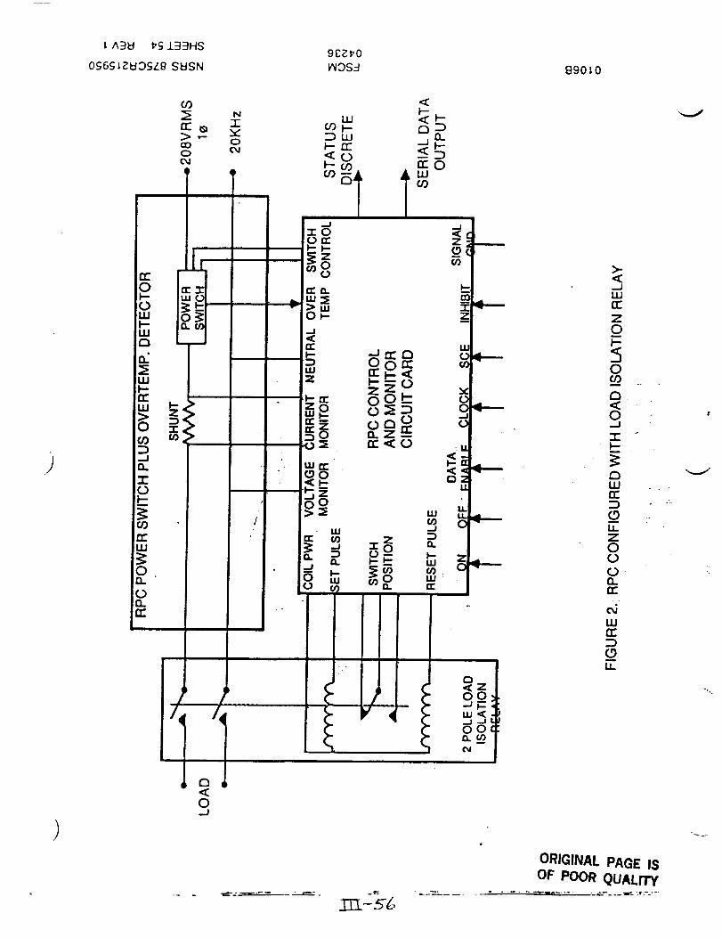
^3_ 17S133HS9C_0
0569 ;ZHOSL8 SI:ISN I_IOS_-I 890 L0
,,=,o_11.
L
(Do.¢r
J
j_lii
uJ <_-cop.. O_
t..- rr<0
°On"
_§ _>w0_- zI rr
g
uO rr col"p:_.< _ 0P'--O
i_ ONDo_ _ o
)0 ,,
0.. I-- _-" w r, 6--.--
_o _ o
•., ,/ L
_Jo_
Wn-
u_
¢7 •<0_J
- • o
ORIGINAL PAGE ISOF POOR QUALITY
. , ,. , ,,.,e."" _" "," . "--__--i.. _- "Ar .'-' ""
.._j
"%.

\
-;k
4k--"""""'----
T20KHz
208VRMS
10RPC
fy-yy'y-y_i
L0AD
FIGURE 4. OFFLINE BRIDGE LOADING OF RPC
1
\.i"-0106B FSCM
04236
EIZ-57
NSRS 875CR215950
SHEET 55 REV 1
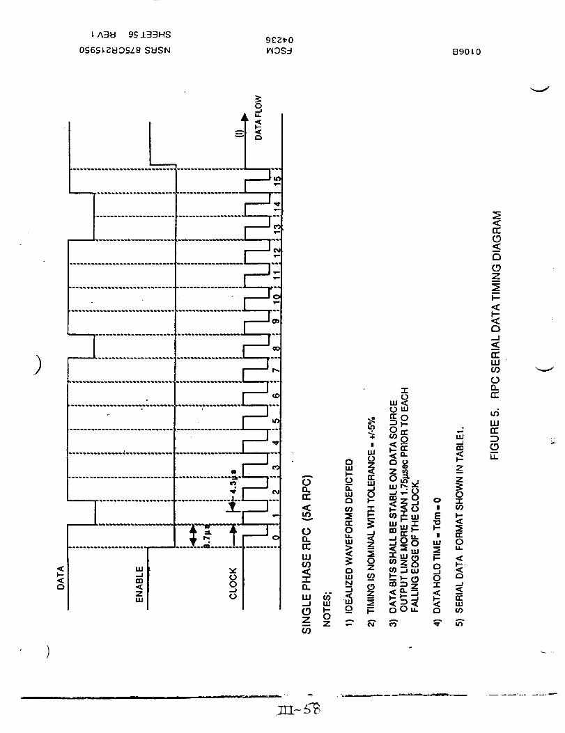
LABel 9S J.33HS
0S6.9I,_C)S/. 8 SUSN 890L0
.o=
.°o #,(l.
o < .oOo _=_ _
Z_ rr-u" |
o _ _OotU
_ o ,,,__.8_ _<,__ _ <
s _'"<-- Z _ _ _" _"O3
<rvrD,<o
Z
I--<F-<0-J
<
rrW00
0nrr
uiUJrr
(.9It.

Final
APPENDIX IV Report
MCR-90-536
July 1990
APPENDIX IV
10 kW DC Remote Controlled Circ!ait Bre_ker fRCCB) Product Control Drawing
This product control drawing was developed for Martin Marietta by Teledyne Solid State
Products. This document provides basic specifications for the DC RCCB power stage.
APPENDIX IV

OO NOT SCALE I'tRAWING

T

Y
.
\,__j-
-o'/
%,'.'.
i:#/

Y
REMOTE POWER CONTROLLER
OUTPUT CURREN.T MS TIME TO TRIP
i
t "1 ! I
• o . . .
. _•. ,
0. 2
0.1
It_ 8_SMOe G RA P_IC:$ / AC_uPRE._S
REO_OEA NO _3_3_t0
300%
i
I
1 ° • .i •
" " . I
; ) i : * i _ " • ; _ I
I i I i | : I t | i | • ! * *
, I I t I I a _ I ' :
i200% "-100%
i
" I • •i t ' .
i I
PERCENT OF RATED CURRENT
FIGURE 1 -:. :-".. : :_'..:', - ." : .....":. .... _"%.";:: . . .- ." . ". :. ....." ; . . ." .. " . r.--. . :
:.-.-,..- . .,.-,,. - ii,. _ • • .
• • t.
• _iOR;C_F'_L
OF POOR QUALITY

FIGURE 2
. : . -. ,; • - •
.... '_:" ' ' " " ' _:,;i • :':'-:.... "- -,'_:.-.. ."._" ...... _ .... ." ,i.., ,
• •:...: . . . •
._.'.'_, "_,.... ..... : -. __-... _. - _. - _ .,. • ., -; .-_..- . :-_.:/:.--. :::. ",-'" ..: .:-"
.o

V
To conduct rated current,-. _....'
all four of the indicated
terminals are required.
. ?. o •
• FIGURE 3 ...
• • " , . ." . , : ... ,_ - . -:" - : , ".--: ,:,_e-,._:._p _ a_ .
FSCM NO.
•63745 I0 - 09C7
ORIGINAL .PAGE IST'q'-'? OF POOR QUALITY
_,_. _;-c. ._, ;: • " :._ - ", . -._ o. _ •..
--'.'. : , ..-'-. : ,-,.L- . "." ." "'.
:::!!i:::

'V'
,i,].50 V o
5V BIASo
I
•L - "" _ ' _"'" " "" "-- " INPUT CONTROL
o o . -
TO TTL LOGIC _.,STATUS
....; ."-..'...;,"_. ._•-
: • ....•.
. ... ,." .. - .:...; .. ._ "_'.," .
., . . .... ._,.....:_.- . • • ._- . ...:. . . .-.. ,..-,-._,..., i,. ..... .... ...
• . , . • .. . # •., • • $ ..%, °., .o•. . : .:...-• . /.." ._ :'. • ...-......:.-._-_.._
, ., ; .-,. ,. _._,...,'.,. :, . ._-._ -. , : .. - . .:. . . - ._,_.._'.';.'.
"Cv" . _ ._" . -...'".'_i'-''_ :, .-... _',.'.._ _...
,k..
CV
_•
• .. ..... . ......
..".".:" :_:_-;-:¢" .':..- ;_...--': :, .-- " • :'." :_ :vG - .; :_'.._:_%".._.4 " ...... "", _ _ . ;o.,.? .- _.. . :.-'-._,%,.._._._. ".•-:.-;_:_.,_":.'"..:.,""_' :'._;.ZL':?'.-u -..,. ...,_. 24 - : ..... ,.-:,.. _,_..._.-:,-,,
• -. :,.',:.'.-_'_ " "_.'.',. .'-. . " .- ,..,-..'._-,_. . , ." .- ." .-v- ,. o .,"
• . .... - ..... .:-. I GND .,...,:_:.a:_" • " _I- .- ",:" .'.:-_. v, - ""'-" "''-*-." -; T ] |
I"_.'._ ':"" ..." ":.':_-_,,': I . . . •
_3;I -"
'......."':.... ILOI'--AO'• "_" , .i "._" _" _ " I .:._'" I
" _:'_";'."i" '" ":""-"',; :.k; ,'- ." i- ..-:
........ •:. .............. "..... ...L-" ., .:,_..,-_. n.-,:.., _. ..... .,.,............ . • ............ _ ......... . ........... "''" • .,_.._.;.._ .-_ ", .- ...- .
_...::- . :'.:. ;,_ -,. ",., - :_ .:. . '. ""., " _. :, :_ . ,..... I50V' RETURN • ''_' _""_ -_""":.":'-..-._''':" " "
O
• .o, •.
FIGURE :;,,.,' " ....::.;:: -: ..
TYPICAL WIRING DIAGRAM ".""
• -o... . . .
°• , ..,•. • .
_':'•:L_',- "
:-,.._, .o . . . - .
NOTE: To conduct rated current, four terminals at output
must be tied together.
oo;o- . o
"..':.-. _ ....... ,.. ...... ., . ._..-.. _.,;-". o . ......... '., . % /. ..
-,&, I_EOROER NO• A;X_70
• j.
;. .., •
• " "-'."- ;"._..- .:- "-'.,--'4.'." 7:. _'. ;. •
.-'.L,._ , ' .... ,' ..'.:.._.--" .. _ : _.._ "'. " ".. .
-. . .... ." - .... .... . -. . ., ?... ...... ,... ._,,_ ,." ..
,%- - • .. ,
SIZEi FSCM NO. IOWG NO.
AI 63745 I IC;O01O - C ] Isc OF
:]3;;C-LP.. ORIGINAL PAGE ISOF POOR QLJAL/'rY

APPENDIX V
Final
Report
MCR-90-536
July 1990
APPENDIX V
DC-400 Hz Load Converter Re_t_rt
This report was produced as part of the previously deleted task of designing and
breadboarding a DC-400 Hz load converter power supply.
APPENDIX V

NETWORK TOPOLOGY
LOAD CONVERTER,
BREADBOARD
TEST REPORT
PREPARED BY

TABLE OF CONTENTS
Equipment List ................................................................................................. 2
Scope "_°I°°=°°°°==_°_°°°°°°°°°°°=oooo=o=o°°_°°°°o°°oOIo=_°°=oIo===o°°°_°°°oo_=_=_==O*=o=oo_°°_°I_°o=_==°°=°_°_toeog 4
Functional Description ................................................................................. 5
Recomendations ............................................................................................... 7
Applicable Documents .................................................................................. 9
Breadboard Goals .......................................................................................... 10
Summary ........................................................................................................... 11
Efficiency and Regulation data ................................................................. 13
Conducted Emmisions data ...................................................................... 14
Output Voltage Ripple data ...................................................................... 17
Open Loop Phase and Gain data ............................................................... 18
Output Voltage Frequency data .............................................................. 21
Output Voltage and Current Waveform .............................................. 24
Appendix .......................................................................................................... 25

EQUIPMENT UST
EQUIPMENT TYPE
Power supply 6227BHewlett Packard
Power supply LR 602Lambda
Power supply LPD 421Lambda
Function generator 3325AHewlett Packard
Oscilloscope 2465Tektron=x
Oscilloscope 2430ATektronix
Current probe A6302Tektronix
Current probe A6302Tektronix
Probe amplifier AM503Tektronix
Probe amplifier AM503Tektronix
Power module TM501
Tektronix
Power module TM501
Tektronix
Freq. response analyzerVenable Ind. 5060
Digital multimeter 193
Kiethley
I.D. NUMBER
541 812
529233
542232
551204
550365
556079
547332
152730
550731
536395
547330
540396
555474
552442
CAL DUE DATE
Ref. only
Ref. only
Ref. only
1 -21 -90
9-23-90
2-18-90
2-25-90
3-18-90
2-18-90
5-6-90
Ref, only
Ref. only
Ref. only
10-8-89

EQUIPMENT LIST (cont.)
EQUIPMENT TYPE
Network analyzer 3577aHewlett Packard
Digital multimeter 87
I.D. NUMBER
561 848
153474
CAL DUE DATE
Ref. only
12-10-89

SCOPE
This report is intended to describe and assess the Network Topology ProgramLoad Converter Breadboard test effort as it applies to proving the concept of the_'-4
topology selected for the Load Converter. Also test data is presented with theintent of verifying compliance with Load Converter Design Goals (Ref. TEO-89-0251) on a down-scaled basis. Additional test data are given which do notneccessarily relate to specific design goals but are of interest with respect topower converters in general. Following the test data presentation asummary/conclusion is given and finally recommendations for improvement ofthe design are given. An appendix is included which provides engineeringdrawings, parts list, and data sheets.

FUCTIONAL DESCRIPTION
The Load Converter breadboard produces regulated sinusoidal AC output power
from unregulated DC input power. The circuit consists of five functional blocks:
pulse width modulator, drive stage, power stage, output stage, and feedback.
The pulse width modulator consists of an SG1524 PWM control chip. This
chip contains a +5V reference, sawtooth oscillator, pulse width modulator with
pulse metering and steering logic, and two complimentary open collector outputdrivers. A current limit circuit is also contained in the chip which is not used
on the breadboard. Implementation of this function would be relatively
fundamental and also desireable.
An external sinusoidal 400 Hz reference is fed into the error amplifier
through a differential amplifier buffer. This signal and the power output
voltage waveform are integrated through the error amplifier and the resultantsignal is fed directly to the PWM. In the PWM chip the error signal is compared
to the internally generated sawtooth oscillator signal. The result of thiscomparison is a pulse width modulated 400Hz sine wave. This signal is fed
within the PWM chip to the output drivers.
The output drivers of the PWM chip are wire OR'ed to allow a duty cycle range
of 0 to 100 per cent. A 74LS04 Hex Inverter chip is then utilized to produce
complimentary full range (0 to 100%) signals. These complimentary signals are
then fed to the gate drive stage of the circuit.
The gate drive stage of the breadboard consists of a DS0056 dual CMOS clock
driver chip. This chip is designed to distribute high frequency clock signals to
a large number of CMOS devices and is therefore ideal for driving a capacitive
load such as a Power MOSFET gate. The output of the driver chip is connected to
the gate of the MOSFET through a 10 ohm resistor. The resistor limits currentto and from the MOSFET gate and damps resonant LC circuit effects. The
DS0056 driver greatly simplifies the gate drive design and helps keep the parts
count low.
The power stage is composed of two power MOSFETs switching in
complimentary fashion, and a power transformer with center tapped primary.
The MOSFETs and power transformer are connected in a two-switch forward
configuration as opposed to push-pull. Snubbers are utilized across eachMOSFETs drain and source to minimize voltage spikes on the MOSFET drain with
respect to ground. Pulse metering logic within the PWM chip assures a certain
dead time is present between the two complimentary switching waveforms.
This prevents both MOSFETs from turning on simultaneously which would
effectively short the input power line to ground.
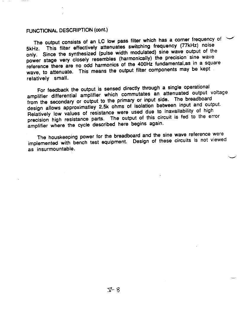
FUNCTIONAL DESCRIPTION (cont.)
The output consists of an LC low pass filter which has a corner frequency of "---"5kHz. This filter effectively attenuates switching frequency (77kHz) noiseonly. Since the synthesized (pulse width modulated) sine wave output of thepower stage very closely resembles (harmonically) the precision sine wavereference there are no odd harmonics of the 400Hz fundamental,as in a squarewave, to attenuate. This means the output filter components may be keptrelatively small.
For feedback the output is sensed directly through a single operationalamplifier differential amplifier which commutates an attenuated output voltagefrom the secondary or output to the primary or input side. The breadboarddesign allows approximatley 2.5k ohms of isolation between input and output.Relatively low values of resistance were used due to inavailability of highprecision high resistance parts. The output of this circuit is fed to the erroramplifier where the cycle described here begins again.
The houskeeping power for the breadboard and the sine wave reference wereimplemented with bench test equipment. Design of these circuits is not viewedas insurmountable.

R_MENDATIONS
Upon completion of Load Converter breadboard test a list of recommendationshas been compiled. The following is a digest of that information. Along witheach recommendation is given the reason or rationale for the recommendedchange.
The addition of a DC servo loop to keep the power transformer balanced must
be investigated. This idea formulated when it was noticed that distortion ofthe output voltage waveform increased when the frequency response analyzerwas inserted in the control loop. Further investigation revealed a switchingcurrent imbalance between the two MOSFET switches. It was determined that a
slight adjustment of the DC offset of the sine wave reference remedied theproblem. The DC servo loop recommended would sense the transformer voltageand feed an error signal to the sine wave reference thus making the systemmore robust and immune to adverse effects of test equipment such as frequency
response analyzers.
A UC1707 gate drive I.C. should be icncorporated to replace the present twochip gate drive comprised of the 74LS04 and DS0056. Although the DS0056greatly simplifies the gate drive design the UC1707 goes one step further byproviding inverting and non inverting inputs. This means the use of the 74LS04to produce comlimentary waveforms is no longer neccessary.
The use of METGLAS core material will improve efficiency of the converter.This recommendation is based upon computer analysis done on the LoadConverter transformer in which several materials such as Permalloy 80,Supermendur, and METGLAS were compared. The METGLAS material was foundto be much more efficient than others due to its ability to support a high fluxdensity level thus making the transformer less massive.
An input LC filter should be incorporated to reduce conducted emissions. Thisfilter must be designed to attenuate conducted emissions at 400Hz. This meansthe filter may be fairly large for single phase output application. Three phaseapplications would not require as large a filter due to higher frequency.
A precision sawtooth wave generator would reduce distortion of the outputwaveform. Although the breadboard exhibited low output distortion under mostoperating conditions harmonic distortion did become noticable under low inputvoltage and maximum load conditions. This meant that the sinusoidal errorsignal was nearly the same amplitude as the sawtooth wave. Non linearitiesnear the peaks and valleys of the sawtooth wave caused distortion of the output.A precision sawtooth wave without or with less non linearity would notcontribute to the distortion of the output.
RECOMMENDATIONS (cont.)
A current limit function should be incorporated, as mentioned in the
Functional Description the current limit function of the PWM chip is not used.
This would be a relatively trivial function to incorporate and is seen as a must
in order for the converter to possess the ability to start a motor. Current
programming of the power stage is an attractive option when considering this
function due to the inherant current limiting of this approach. Other benefit are
to be had with the current program approach as well: simplified control loopdesign due to single pole filter response for example.
The direct sense feedback amplifier must be redesigned using higher value
resistors. This would improve isolation between input and output affordinghigher common mode voltage rejection in the system.

APPUCABLE DOCUMENTS
Technical discussion
from change order #16
Engineering Procedures Directive
Operations Directive
Enclosure 2 toTE0-89-0251
EPD 849MWT
203627-100-20

BREADBOARD C_)AI_S
The goal of the Load Converter breadboard is to prove the concept of a two
switch forward converter with a sine wave reference producing sinusoidal
output power.
This is a key milestone in the development of such a converter since this had
never been done at MMAG. Secondary goals consisted of verifying parts stress
levels and circuit performance with the idea that this data would drive design
nuances previously unrecognized. These refinements are difficult to to identify
and quantify through even the most rigorous analysis. Proof of the concept of
the converter is believed to be a success and design refinements are given in
the Recommendations section of this report.

SUMMARY
The Load Converter breadboard successfully produces well regulated, low
distortion AC output power from unregulated DC input power. In conjunctionwith the recommended design changes discussed here it would be a simplematter of scaling up the basic design to achieve the original power level (175W)intended for the Load Converter. An on board sine wave reference is most likely
the most significant task remaining. This along with on board housekeepingpower capability would yield a fully self contained unit.

TEST DATA SECTION

EFFICIENCYAND REGULATION
EFFICIENCY
Min. line (10V) max. load ( 1 ohm) ............................................................................ 21.1%
Nom. line (15V) max load ( 1 ohm) ........................................................................... 18.6%
Max. line (20V) max. load ( 1 ohm) .......................................................................... 16.8%
Note: There are two main contributors to the low efficiency of the breadboard:
1) Low output power level by design. 2) Output filter voltage drop; in a DC
output converter this paramemter is negligible however with a 400Hz output
the inductive reactance of the filter drops the output voltage seen at the load.
Further investigation is required in this area to optimize filter characteristics.
REGULATION
Min. line (10V) max. load ( 1 ohm) ......................................................... Vout = 3.97 Vp-p
Max. line (20V) may load ( 1 ohm) ......................................................... Vout = 4.06 Vp-p
Line regulation .......................................................................................................... 2.2°1o
Load regulation from 10 ohms to 1 ohm (resistive) was less than one per
cent including power factor excursion of 0.9 leading to 0.7 lagging.

CHlgnd_
I
CHI
I I , I I I , I i
LINE CURRENT (CONDUCTED EMISSIONS)Vin = 10 VDC (rain. line)
max. load ( 1 ohm)Verticle ,, 0.5A / div.
Horizontal = 1ms / div.

CHlgnd_
- ii!i
I I
i
iiiiiii!ii,i_ i i i!.i!i!iiii_i_-;!..._!_ !i _E "_:._.:: i i: 5" _: _
-_ ..,r _! if! I]_!ii_i"_i iii "..'l':.'-'[ii"i!11it -:]i__i!i_i!i!1_'liii,_iiiilL;i! I :: r. i "1 " I I L: "4 _l i'l _1 !_1 I ': I;: t '.-.-'1
I I I I
I
i !" i !
": ,:_ii ii- !i 11ii
i ! i H :i
"iil i!iiii IilNL
il: I
i!ii_7!Ii
iiii ! i',i _] i i_! 17 " "
ii ii ....!'_i!i! i:_
!ti!iiii...,i il i.- _,_! i
: : : ::: :: : :: :
t'i ii iii i!iiiiii!. _, -i:.:" _ E_ !ii iE!iill :, i i::i!ii7............L:,: _li E!_:.E! i .: ::: .r: :::::::: .': :. :: = :
_,__:_ : i_/:.-, ili !i iii_ii_ii!i_ii ii.r:..,ii-_-_
i! il ......... 't I i__i_:_-_
I 1 I I
CH!
LINE CURRENT (CONDUCTED EMISSIONS)
Vin = 15 VDC (nom. line)
max. load ( 1 ohm)
Verticle = 0.5A / div.
Horizontal = 1ms / div.
{t-,_/;7:_i_ PAGE IS
OF POC't! Q!J_LI._f'

I • I I I _ I I I |
I I I I I I I I
CHI
LINE CURRENT (CONDUCTED EMISSIONS)
Vin z 20 VDC (max. line)
max. load ( 1 ohm)Verticle - 0.5A / div.
Horizontal z 1ms / div.

CHZgnd_
I 1 I I I I I I
, , I , ,il, t t , , I r , _ , I i , , ," , , , f J , I , I I I J t I I t!i J I I _ , I I I
.... I I i I i fill i i i I I I I i 1 t I I I I I 1 i I i I i i I I i t I I I il:l I I 1 i I I /...... •......•..... -'.."i i.'.:_:..'-'-'.-'-'...-'-'-.-:............-..,...... " !ii: .."....
• _'! ¥_"';':".***" :._.._ ..:.-. ......
I I I I 1 I 1 I
CH2
OUTPUT VOLTAGE RIPPLE
Vin -- 20 VDC (max. line)
MAXIMUM LOAD ( 1 ohm)Verticle = 0.2V / div.
Horizontal ,, 2us / div.

| v • I IIIII I I I I IIIIi
::i :
OPEN LOOP PHASE GAIN MEASUREMENT
MIN. LINE (10V) MAX. LOAD (1 ohm)
_3T--2D
ORtGII_,_AL PAC_ IS
OF POOR Q_JALITY

I • I IIII I I I IIII;
OPEN LOOP PHASE GAIN MEASUREMENT
NOM. LINE (15V) MAX. LOAD ( 1 ohm)
ORIGINAL PAGE ISOF POOR QUAI.FI'Y

l I I i lill:i • • I_IiI
OPEN LOOP PHASE GAIN MEASUREMENT
MAX. LINE (20V) MAX. LOAD ( 1 ohm)
_-2ZORIO_NALPACEOF POOR Q(,/ALtl"y

REF LEVEL
-60.O00dBm/DZV10.O00dB
MARKER 400.O00HzMAG (R) -69322dBm
r
• .-?
STARTANPTD
f
L
R
I
100. OOOHz-_O. OdBm
STOP 2
'_"_v't'_J_I '1
,!1i
J i_OIO.O00H;
OUTPUT VOLTAGE FREQUENCY SPECTRUM
MIN. LINE (10V) MAX LOAD ( 1 ohm)
"-'Z.3
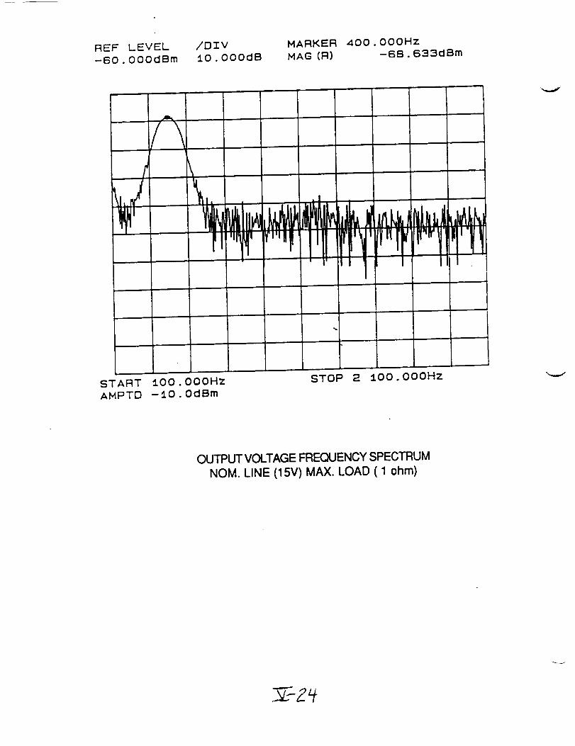
REF LEVEL-BO.OOOdBm
/OIV10.O00dB
MARKER 400.O00HzNAG (R) -68.633_Bm
FI
J
I
STARTANPTO
A
i i J
m
lO0.O00Hz-lO.OdBm
qRIII _'J_:
STOP 2 lO0.O00Hz
OUTPUT VOLTAGE FREQUENCY SPECTRUM
NOM. LINE (15V) MAX. LOAD ( 1 ohm)

REF LEVEL--60.O00dBm
/\
!
/DIVlO.O00dB
l'V
MARKER 400.O00HzMAG (R) -58.825dBm
li IMI.
IVl r 'plOw'"r
START _O0.O00HzANPTD -_O.OdBm
STOP 2 _O0.O00Hz
OUTPUT VOLTAGE FREQUENCY SPECTRUM
MAX. LINE (20V) MAX. LOAD ( 1 ohm)
._'2E.... o _ .

CHlgnd--, , , , I i i t v:l * i I i 1 I i J , I _, ,
e"
I I I l
.." ".._
"_:.
/ -+
, , , J J I , , ,.r:l , I , , I , t , I I ++, , ,
.p"
+,:
7 "+
.+P v: --
/
• "..+ ._o I.++'*;
J 1 I , I •
CH1
OUTPUT VOLTAGEWAVEFORM
NOM. LINE (15V) MAX. LOAD (1 ohm)Verticle = lv/div.
Horizontal = 500us/div.
___-_ (_+++;+_++:+_.PAGE ISOF POOR QUALITY

APPENDIXENGINEERING DRAWINGS
AND DATA SHEETS
Z-27

_'_
I
"7
----._
I>
0
0
©
J
J
CP..!_;NAL PAGE !S
OF POOR QUALITY
v

: 2, ?Op
+/2v
LIo.'/ b,_:"_.
f
ORIG_;_L PAGE ISOF POOR QUALITY

4,,.4
L- _ ,
;{
SILICONGENERALr
LINEAR iNTEGRATED CmCUITS
SG I 524/SG2524/SG3524
REGULATING PULSE WIDTH MODULATOR
DESCRIPTION
Th_s n'_ Wtie_'aled _ oonUdlls all the (:ofltrol ck'cuitry for a
regulatinO pov_ suplW mvecw or sw_chktO regu_t_. Indudedin a 16-
i_n dual-kl..MwI paOcago is the _ reference, ecror amplifier, oscillator,
_tse w,dm n_u_to¢, pulse stee_g flip-_p, du_ de,_UnO output
swtch_ and current liming and rJ_ut-do_ _. Th_ devCe can be
used for iwitch_ regulato_ ot eiltmr I_larity. transicmw coup_ DC toPC conveners. _anslc_nedesa vo.aoe doublersand _ conveners.
as wee as olt_r power applications. The SG 1524 is specifw_l Io¢ol_fation
over the full military amC_r_ temperature range of -55"C to +125"C. _e
SG2524 for -25"C to 45"C. and U_e SG3524 is ¢k)_twKI Io¢ commercial
a_mations of O'C to +70"C.
FEATURES
• IIV to ,10V ol_ndton• 5V eMee_moe
• Rofefence line Md load regulation of 0.4%
• Rof_mce lempe_tum coefficient < 2 1%
• lOOHz to 300KHz o_dllato¢ range
• Excellent exlemal sync ¢ml_bllNy• Dual SOmA output tmmdstocs
• Cummt limit ¢trc_n/
• Complete PWM power control clrcuit_f• Sl¢_le ended or i_al,-i_lt
• Total supply currant less than lOmA
HIGH REUABILrTY FEATURES . SG1S24
• Available to MIL-STD..883B and DESC SMO• MIL-M-38510/12601BEA - JAN1524J
• Radiation data ava,ilabla
• $G laval *'$*' p¢ocesMng avallabla
BLOCK DIAGRAM
VI N RI[F(R(NC_ +SV TO ALLR_GUt.arO_ - = INTERNAL CIRC;. '_Y
._L.OSCILLATOR
OuTPuT
(A
+5V I +5V
'NV. 'NPUT _ O__ . ¢j[Nrrj_
'" "'-r_, 1968
ORIGINAL PAGE IS
OF POOR QUALITY
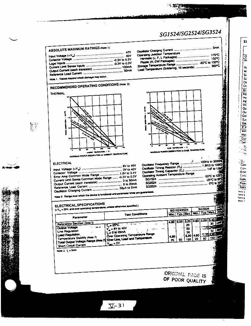
SG1524/SG2524/SG3524
ABSOLUTE MAXIMUM RATINGS INom1)
Im_ vo_Qe I+v,,,).......................................................... 42vColk¢1_ vo0_ ..............................................................4orLogic inputs ....................................................... .0.3V to 5.5VCu_rm_tL.imil,SenseInputs ................................ -0.3V to 0.3V
Cum_ (eac_ _rar,_) ....................... _0on_Ref_'qmceLoad Gumrent............................................ S0q_A
O-_Ua_ C,mmnQ Cum_ .............................................. SmAop_a_o Junc_onT_r=umHernw_c (J. F. L Packages)....................................._7S*C
(N. 0W PaO_Oes) ........................................_so-cTemperatureRange ....................... -65"C to 150"C
Lead T_om'ature (Soldedng.10 seconds) ................ 300'C
RECOMMENDED OPERATING CONOfrlONS INoN 2)
THERMAL&S
12 x,,
ELECTRICAL
In_ vo_e (,,v,,,) ................................................ ev to _ovCollector Voltage .................................................... OV Io 40VErrorAmp Common Mode Range ...................... 1.SV_o3.4VCurrent _ Sense Common MoOeRange ....... -0.3V to 0,3VOutput Current (each transisto() .......................... 0 to 50mAReference Load Cum'ent....................................... 0 tO20mAOscihtor Charging Current ............................. 30_ 1o2mA
|
osc_ _ Range ............ /.......... _OOHztoOsddk_ Tm_O Rem_x (P_) ...................... _.SK_ to
T_ni_ _ (C_) ........................ArrX_ Te,'np_'_ Range
SG1S24 ...................................................SG2_24 ......... . .................... , ...... _ ......... ..o.
SG3S24 ........................................................ 0"CIo
ELECTRICAL.SPECIFICATIONS
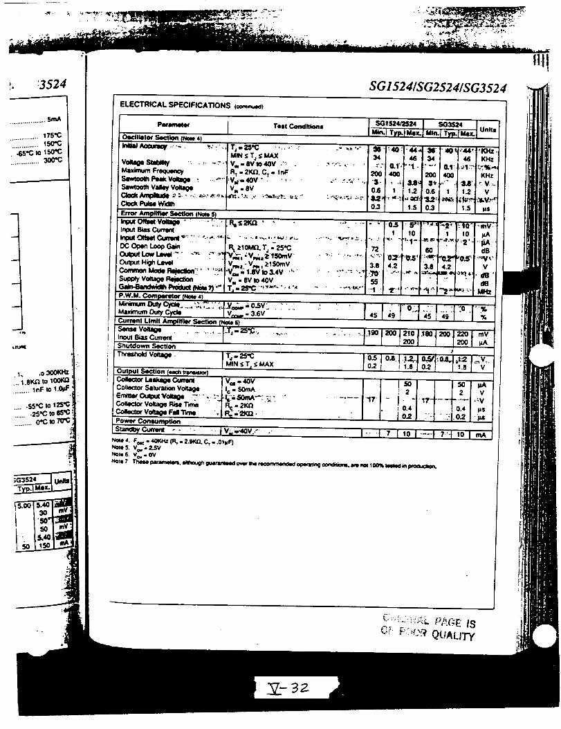
_. 3524 SG I 524/SG2524/SG3524
................... _fT_
;G3524 _ i
_1T " •
ELECTRICAL SPECIFICATIONS |com,_u.d)
Pmrame(_r Test C<)¢Klitk_ts
OscmetorSection[Nom4)IniUlAOmnW ...+. _.=: .•,
Maximum Frequency
Smmx_'tPuk VoUge : ......Sawmo_V_ VoUgeClock J_/IqpiBXle z_3. • =+_+:,r._.- J: +!,_4cIo_ Pu_ w'mm
• Sr_ Amp,W S_,o. 1No*.S__n_ O_ V_ ........
MIN <_Tj _ MAX
+4.- IIVto 40V .'_: . :' ""= ,. :R1 - 2KJQ,CT - tnF
'Yi'- 40V "*, +,, .,' _!,_" ' ,,V., - 8V
} sG_sz*azsz4 I' _3s:4 !• _ I UnitsPAin.! T]tp._ MaL I MIn. I Typ.] MaL|
InputB_s_
OCO_m Coo_G_OulputLowt.evel_"" _ "_'""Ou¢_ H_h Le_
Supp_VOaag*_
P.W.M.Compm_or I,o_ __,w,_ D,_ Cym.... 0,7:: ',..Mm,murnOu_ CX_Current Limit Ampl.ifl_ Section {I
:iS =40 ,44, 3S _0q;44,. "KHx.34 46 34 [46 KHz
:+-- 0.1",+°1 • '"" 0.1" ._1::'!;_1_ ,'_
2001 400 200 400 KHz
"$- ,:._ _1.8_ :1_ • _A:_ _,V:_.0.6 1 1.2 0.6 1 1.2 V
0.3 t.S 0.3 1.51 I_s
RuS2f(D ....... ....r . • . ,
R_ 'V,,_,ZS55mV ...... "......""+ <';+Vm, - V m _ZlS0mV 3.8
"V_, - 1.0V tO 3.4V "+"_: "'.' :.?0'
_Ym - BV to 40V 55
'T_- ;_"C"_'_"'i"'"+' .... ....."_'":"_
.V_ =O.SV- .... ._ I -vm... 3.sV " , 4s+
_,,sI
0.5 • 5+'_r_''."_2-" _'I0.....mY:t lO 1 1o I_A
P
I......I'1 ":'_'='_+'' =2.... _:60 dB
• _11_" ,r'=V _"l 0:Z' "O..S'": ._' v0._:4.2 3.8 4.2 V
,,_ .... ,-+ J, ,51 l'+ _-',_ :A+,MIJl_ _*
+,+To-..II+:++.o.r+l
! InDu1 Bias Cun'e_
ShutdoWn Sectio_
Thmsh_dVoUge
.... ........ _T,- 2S'_-, ,,_....
Output Section (_c_ Inm_or_Coaec_rL,m Cum_Collector Saturation1 Voltage
em_Ou_Vo_e :-+ ..D:Collects"VoltageRise T_mo
Colec_ Voltage Fal The .
l o.s ._.2_o.,.I°"! o+ii _.+I v
155 i soi 2 2 V
.... _--- 17" I" -'17 ....... ':V0.4 0.4 ps
: lo= "- " ::.-o_+ "_
I _0 i---f 7'-1 "10 I mA.Power Conwamptkm
V_,. 40V
Ic - 50mA
.I,:--SOMA"::_ - "
s_,_ _ . - .-- :;-.lv...,,ov...-.... I-- 1 7Pim, i. F_,=. _*(Hz Oct,= 2.W(O. C, • .01_F)Nozi S. V_,. 2__VNOle6. V_, - 0VNote/+ These _. a/moug_guarameed o,qwm* .x=omme_ 0Om'a_ng¢ondi_ons.am no( 100_ mm_i kHam4u¢la_
0_: P:::_OR QUALITY

t
_r SG 1524/SG2524/SG3524
_ J
,Or .OZ
I=_GU_E t. OUTPUt' I11'_II 01_01rua_ vs. C,
.n_ 4A
Note Iha! for buckragulal_rtopo6ogies, the Iwo ou_ut_ can beu_re-ORed _o_an _MaMI 0-90% duty c'_ tango. Wcth_'_sconnectS, me _ frequencyis me same -,_ me osc_w_lu_"y. Fc_pus_p_ _akae_ns, _e ou_u_s _re useclse_rme_: e_ene-no_ r,e_ meclmycyclerange ._ e_cn cx4_u_m o-45%, and me _ mv_:t_g fmquoncy at me nn__s _,2 tmnoseaumr e_mcy.
I/i_is clesJ_ tos_ me SG: 524 _oanexlomal ctock,a_s_uve pu_4_may be apl_ _o me ck)ck _n. The o_mrs_u_ _e m)_nv.ed w_ R, and C_ va_es ma_ aue _ m/me.run m__X, 0_ me oxten_ Wnc frequeecy. A sync puleew_tha max_mJmIo_¢ 0 of .0.3 vowsand a mi_num iogk: 1 o_,+2.4 volts_ to Pin 3 wWIlock Ihe oscilbll_ to b',teextem_
_e,_r,_ne. Th_ c_x_ pies_ulcl nov_wbo ar_m morn n_Fuh_,
/ CUFIRENTLIMI_'_
I Tho cu.en! i_m_JngC_rcBy malc_r_ It_ I:_assum_a neg_e
C,L Thres_. v,-2c
_ miscirc_ _cneg_g_ lemi_rat_m,
The mosf im_orlant ovo/tage_m_o: ,0.3 vo_,n the groundOrmtUm k_st_jk_ b_ _._..4nfonol b_,megraem_circuit ovenc_arr_diode ll Pin S rnaachieve _s.
A_ factor to COnsks_ow. The Current_rr__.,C, andOl,msu/bn
h
•_,..__,s_,.;.;oT.
,- ahase COmloeflsa
OF POOR QUAL

can beW_t_ mis
oscilUllOCare used
me tfanl-
,os_tor
_au_e _to
_nc pu_e
e_m_al
_0 nanos-
, ,ec_red
• nega__enom_l-25% over
Ire<:lUenCY.
Tf:_n$IO the_oc__n o_.. _ sync
gel'nee.
SG I 524/SG2524/SG3524
APPLICATION NOTES (conlinued)
CURRENT UMITING
The curren! limiting cin:uitry of Ihe SG I $24 is shown in F'_me 3.
By matching _ base-emitter voltages o_ O1 and 02. and
assun_ng a negligee voltage drop across Rt:
C.L. Thtestm¢l = Vm(Q1) + I,'R, - Vm(O2) = I,'R=- 200mY
Although this _ Ixovides • _lSChNDly¢_ _ _ a
neg_lil_ele_ c_ lhecea_e soe_ le_moes Io
its use becau_ o_ _ siml_i_.
The most i_umt of _ is me limited __
vot_ge ra_e: _0.3 _ amued greund. TI_ _ui_es _ee_ng
in me Oround o¢ return line _ me powe¢ sul_/. Also Wecau_nsshould be Ud_n to rm uxn on the paras_ submnm diode o_ the
int_raled circuit, even _ lrln_eN conditions. A S¢_oMk'y
c_mp cliode _t Pin 5 may be rmquin_l in some con60u_ations |oachieve It_.
A second fac_r m eonmd_r m mat a_e rem_nm, tim_ i_ m4a_ive_y
stow. The current _ _ is intem_ly __ by
R,. C,. and 01, resulting in a ro_-olf po_ alap_ximate_y 300
ERRO_
AUPLIFI[R
HZ.
pins. A oo_4ant cun'_nl ol _owo_rnal_ 1501zA 0ow_ out o_Pin
4, and a vlmd_ currm_ wilh a range ol 0-150_A flov_r,out of PinS _ a ruuIL _ _ souse i_(la_e aen I_ _
Current sense i_ns should be less than 50 ohms to keep Ihemmshold emir less Chin 5%.
S_c. U,4 _in o4 tins cin:uit _ ro_aMdy k_w (42 dO), mere Is a
transition region m me cun_nt limit ampr_er takes over pulse
wiam oon_ tram me enot wnpifw. For tmmng puq_m,
t_eshold is deSned as the k_ul voilage requimd to get 2.5% duly
cycle (.2 vows .* me erro_ amprme_ output) with meampler _ondno maximum d_ cl, de.
APPLICA TION NOTE: ll ltm cutrenl lkwil _ _ not _ed on
the SG_524. _e ¢ommee-mode _ range m_icboe re*
_ t_e_ cunw_ seese pim _o ae gmueC_L
• . ,._ bI
i
I
3 - ¢u_Nsl_r kwrlrmO _U_YMV O_ _ SO_
:----4,,, : 1 ;
'. m,s conventional stogie-ended regulatm' cin:uit. Ihe two out-Outs of the SG 1524 ate connected in parallel Io_effective 0 - 90%
_uty-cycle modulation. The use of an output inductm' rm:lmres
a_ R-C _ compensatmn network ira" loop stabmty.
4
•I,,,, I --
-'0
Push-m_ll ou_outs are used in this nnskx_mcoulded DC-DC
mguiati_ ¢onvecte_. Note Ihat Ihe osdllat_ mu= be let at I_e
me cles_recloutput fr_luency as the SGt524"s internal nip.flopdivicles Ihe Ireclmmcy by 2 as il s_O'_l Ihe P.W.M. signal Irom
one oum_ to me omer. Cum_ imi_g is clone here in Ihe
Wima_y so that me ix_e wklm .4 be rKluced should mms-foml_r s_uribon oc_Jr.
ORtC,,_.tIL PAGE ISOF POOR QUALITY
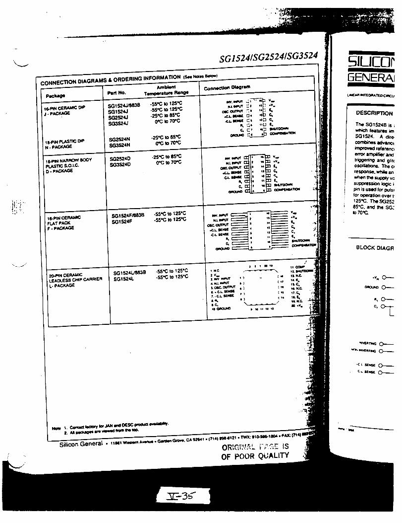
o._
SG1524/SG25241SG3 524
Peck_
CONNECTION DIAGRAMS & ORDERING INFORMATION |See N_es Sex)w)
Port No. Connectkm Dtogmm
I(FPIN C.EI_IdM_ DiPJ. PACKAGE
16-PtN PLASTIC OIPN - PACKAGE
16.PIN NARROW BOOY
PI.ASI')C S.O.LC,
[ 0 - PACVJ_3E
lr,-PtN CERAMICFLAT PACKF - PACKAGE
20-PIN CERAMICLEAOLESS CHiP CARReER1. PACKAGE
Tempe'am Renge
SG152¢I/8838 -$5"C to 125"CSG1524J .55"C to 12S*C
SG2524J .25"C to 85"C
SG3524J 0*C to 70"C
SG2S24N -25"C to 8S"C
SC_1524N 0"C to 70"C
SG2524D -25"C to 85"CSG3524D 0"C to 70"C
SGI524F/883B .55"C to 125"C
SGI524F -55"C to 125"C
SG1524U883B -55"C Io 125"CSGI524L -55"C to 125"C
I NIC
2 Vw] INV IM_UT
S 0_¢, OIJfl_'f
7. - ¢_. SCd_[
t.¢_
_._ wrEo_,TED CmCu
DESCRIPTION
The SG/S24B is
wh_ lea_ures/m
5G1524. A dire,
conches ao_u__l_:w_l referenc,
error am_/fk_r and
tnggehng and g_(oso_. The o
response0 wh_e an
_ is used for _._
for c_oerabon Over I_
_25"C.TheSG252BS"C. and _ SG:Io 70'_
BLOCK DIAGR
.v. C>---
Nine _. Om,u_ordANan_DESC_m,*_.='. Aa _ wl, m,,,_l ¢mmme t_.
J

¢t
u)
ORIGINAL PJ
OF POOR Qt
National MOS Memory Interface CircuitsSemnconductorDS0026, DS0056 5 MHz Two Phase MOS Clock DriversGeneral Description
DS0026/OS0056 _e low cost monolithic high sidled
two I=hm MOS dock drivers and interface circuits,
Un_clue cirmit d_tF) I_rov/d_ both very hig_
Oll_rltiOn and the abiliW to drive large capacitive loads.
The device acceDu standard TTL/DTL output=
corwe_l$ the_ to MO$ Io_ levelL They may be driven
from standard 54/74 _ies and 5451745 series gate=
and flil_flo_s or from drivers such as the DS8830 or
DM7440. The DS0026 and DS0056 are inler_ld .for
aOl_ications in which the output pulse width is logically
controlled; i.e.. the output pulse width is equal to the
input putN width.
The 0S00261DS0056 are designed to fulfill a w_e
variety of MOS interfltx, requirement=. As a MOS clock
driver for Ion 9 silicon-gem shift registers, a single device
can drive over 1Ok bits at S MHz. Six devices provide
input address and _'echerge drive for a 81( by |_bit
f 103 RAM memory system. Information on the oDrrect
usage of the 0S0026 in these as well es+other systems isincJuo_d in the _ication note AN-76A.
The DS0026 er_d O_0OrJ6 are id_mtical except _aeh
driver in the O,.R0056 _l provided with e Vee connecrion
to _ul_lv a higher voltage to the output stage. This aids
in Dulling up the output when it is in the h_ state. An
external resistor tied hetween these extra pins and a
_I_Y higJler t_lm V ÷ will ¢auN the output to pull uPto (V + - 0,fV) in the off' state,
For DS0056 a_ications, it is reQu/rad that an external
resistor be used to I)re_nt damage to the device when
the driver switches low. A typic&l Vie connection is
shown on the next page.
These devices are available in 8-lead TO-S. one
copt_r lead frame 8-pin mini-DIP, and one and a half
watt ceramic DIP, and TO-8 packa_s.
Features
• Fast rise and fill times--20 ns with 1000 pF load
• High ouq=ut ¢wing-20V
• High output current d,rive--_l.§ amiss
• TTL/DTL ¢orrq_tible inlets
• High _ _lte-5 to, 10 MHz depending on power
di_l=etion ............
• Low power Conmml0ti0n in MO$ "'0" state--2 mW _
I Drwet to 0.4V of GND for RAM address drive
Connection Diagrams (TopViews}
TO-S Pa4kSlle IC)u_4_-Lme P_kale
" l' I' I' ':_4 meeemew_ I¢ m& V" roll
1"04 P_ka_
v"
GE ISIALITY "-' *"--
N_ OSOOMI4
S4e NS Psckqle HO_C
TO4 P_ka_
(w4
' I' I' 1'limit. Ill& _/" IIIIIII
Q_I_
_ p,,,,,_,_ .
If' I¢ III_I II III
I¢ I_ IlVl I_ IIII_ III
Ik_ NS Pmkm FI4A
=¢ K
!lec
v_u
I_e 4
117- ,',e
-3b

3ircuits
Drivers
t is in tt_ high Still. An
these extra pins and a
;e the outPUt to pull up
equired that an external
_lKle to the device whim
)¢al Voe connection is
8-1eKI TO-5, on_ watt
lIP. and one in¢l • half
:kages.
ns with 1000 pF Iold
: 1.6 amps
• ::. ..... _
4z depending o_ power
• MO$ "0"'rote-2
or RAM addreSS drive
'IITI l¢ ml ,l¢
NS PIklll Flibk
,solute Maximum Ratings (Note I)r*- V- Differential Voltage 22V
inPU I Current 100 mA
_out Voltage (V, N - V'l 5.5V
Outl_J t Current 1.5A
rical Characteristics ¢Notes2and3)
Operating Temperature Range
DS0026. DS0056
OS0026C. DS0056C
Storage Teml_erature Range
Lead Temperature (Soldering. 10 seconds)
R,ll Time
Fill Time
rPARAMETER CONDITIONS
LO9,¢ "t" I_l Voltixle V" • OV
I,_ LOtp¢ "1" In_! C_Jrrent V m - V" " 2.4V
V_L Loel¢ "0" I_put Voltage V ° " 0V
IK LooN: "0" Ir_Jt CurrenI Vw, - V" - OV
¥,,_ LoeK "1" Oulpu! VOaIIIW Vl_ - V" o 2.4V
Vo_ Lc_l¢ "(T" Ou tllUt V_ la_ V,_ - V- " 0.4V, Veal > V_ 4" 1.0V ! 0S0026- 0S_056
_'_,_., "ON" Cur,_l V + - V" - 20V - V" - 2.4V DS0026S_X_V V_
lNose 6l io,_ s6d. _) DSO056
_'_'_j_ _, F" V' - V- - 70°CPeOF Supl_V C.rrem 2OV.
VtN -V- - 0V 125°C
Characteristics (T, - 2S'C)INot. Sand7)PARAMETER CONDITIONS
Turn.in Dtlav {Fqure I/• i
• fFifum 2}
Turnmff Ocdiv {F_e _,1
: (Fap.,m 2/ "
{Fqwm t/. el, - SO0 pF .
fNom 51 C_, • 1000 pF
(FqpJm 2_, C_ r = 500 pF
(Note SI Ct. " 1000 pF
{FillU_ l,/, C_. = _ pF
(No= SI C_ " tO00 pF
-55°C to +125°C
0=C to *70"C
-65°C to +lS0°C
300°C
MIN TYP MAX UNITS
2 15 v
t0 tS mA
0.6 0.4 V
-3 -I0 .A
V'_0.7 V'tl.0 V
V"-t.O V°-0.7 V
V°-0.3 V*-0. I V
30 40 m_
12 30 mA
I0 tOO uA
10 _0 MA
I TY_ MAX I UNITS
i
!: ;_ t2 --i
I 11 _,i
12 1S ns
13 n$
IS 18 n$
20 35 n_
:30 40 ns
36 50 n_
12 16 ns
17 2S m
28 35 , m
MIN
§• -
{F._n 2/. C b - 500 pF J(Noll SI Ct. " 1000 pF j 3t 4o .,
i
I; "'AbIOlUN MalCmrl_Wl Relmgl" _ _ vlllull _ i_h_h Ihe Ilfet¥ of _ ¢klv_ll Ial=_Ot be g_ranNNl_. EXCalOI for *'Ol_flltin_i
Raleq_ "° _ _ I_Ot ffllll_t IO _l_y _ _ ¢_ li_o_l(I I_1 _fl|ll_ II I_ IIl_tlB. The tiOkl of "*Ele¢lr_=ll C_l_rll_ll_rlllld_*"
2: Thell Ig_l¢it_¢alllOnl Ibl_ly |or V + - V- - tOV IO _f, C L " t000 OF. _ _ _l_l¢lWllR ¢lk_gl of _JS"C Io • t2S'C I_" me C_OO2_,
• 70"C to,' _ DSOOE. DSOOS_C.
2; All IL_rrlfftl_l inIo _ I_l_l _ II I_lS_tl_t. _t Of _ I_nS i negatn_l, all _ta_l ralll_lfl¢ll¢l tO _r_/nd unllll O_4N_eall et<lll¢l,
i_ valulS ShO_ i m&ll i_ mm on albloIuII Vllkdll b_l_.
All t¥@ICalJ viluel for _ _A = 2_'C.
R011 al_l talll Im_ alee l_li'i tcr MOS lOl_C levlN; i.e. rill llml i Ifal_l_lim,i from _ _ to _ "t" wrt_clh ill vo41111 IIII.
iilil I_ O$008_ iS m_mzm_a_V (VBI I - V--ilt i_l |ira _ _le| _ m_t il IOw.
7: The kil_ _¢ wmNim {m _ "u l.liAI _ Ike _ el the _sm_li _mll V- Mid dwell I1_ eillml wmtm
etal hills mle m I_ll lille m ill_l_' i Illtl_ II Im fill ml=,_t. I f Ill• alileh_d imlmralo,lAl_.-Imll lexd f fires Ihe Ik.im_a ckmudt tm
Iottl. Or has illsitmt dc fliltm_t, iS m luiCem flrll_ lie sw*t_hmtl nm_lmm.
VBB Connection DSOOS_
_o*lm
r • -i_
OF POOR
(/)
Q
o')
3E Is
-37

¢ •
)
IL
mK.I
cOIt)
r_
r_
Typical Pertormance Characteristics
InPut Cun_ml _ Inlml Vollml_
Ill _-- ------I ----_
..-- [
-' ,-_ ...., -_-
-IJI4J I U 11 1.$ I1 IJ_
$41k_UTVOLT&G|_
_o_rqml _ To_qmrstul_
]l_lhrtYCLE-_...J.._.__ --
t-tldlk I
-N -M -IS II N M N III IH
TIl_f.l_t IU ('a
T_ md i'vrn_
w Tewwermure
|4 ---_--- ,--,-
Rim 11me _ ¢Jml
,i iII
|
e MII _l Ill ,hi _eM (_
Cdl_iC.Ct_CCl'MClf _;
r.em Xlme w _
!- II
14
G INIq Im
_tlll
| ,-8 m
mm
i'.
11,
IN
lU
_M
m
111
m
I
_M m _ M8 MIOM _ M_
f
N • M 41 M _ N III
_*_,_,._-,,- PAGE IS
.OF POOR QUALITY
Turn-On _ Tv_ff
I,i Teel_ewMw'e
!
n
I _°n
:
!
: _
-I -n | _ N
1' agtCmT
_D
T OP °
L __..,,j
am 10111 8m
,ce Iol;I
N m U
ernatic Diagrams
IlYlllnL_C,,,
vii
in osoo_
in DSOOS6
(/)
(n
(31
"_- 3q

I
i
l
.3,
"T.
Gl
¢d"
AC Test Circuits and Switching Time Waveforms
,.L,.. -- LI-J Z
FIGURE 1.
±
3TT
FIGURE 2.
Typical Applications
J¢ ce,li_4 MOI Cllli D,Iv_
i'=11_
C
i,:. OSO0
:¢. The c
m4!Nl_
.,.;, ,o, ,,vOIll9
-- provic
qnPuts
__ suppl;
the s_
clesigr
_' " probi_'
• - L,ne r
freque
the cl_
.v,,
o
Drk_ lPldtl__ o,w)
,MIIv
OD;p-m,'='_ PAGE IS
OF POOR QUALITY
VR
could I:
_'O| tlcJe
Vss -#re tie(
turning
m_rgin
it _S e4
time ca
Contro(
b,emaus(
_r_ng.
In this
tin be
minimi;
Olm_in
_ies
Since al
¢_ock s
much f
rE_llStOf
minimu,
bec._K_$e
reSisTor
the _)¢lu
OOhmu_
k

\
r----i
-J,
=M,lw
Application Hints
DRIVING THE MM5262 WITH THE
DS0056 CLOCK DRIVER
The clock signals for the MM5262 have three require-
ments which have the potential of generating problems
toq the user. These requirements, high sc_.d, large
voltage swing and large cepacitive loads, confine to
IxOVKle ample ol_ormniW for inductive ringing on dock
lines, coupding dock signals to oth_ clocks and/or
inputs and outputs and generating no_se on the power
sul:q_ies. All of these proolems have the potential of
causing the memory system to malfunction. Recognizing
the source and potential of these problems eidy in the
deign of a memory system is the most criticJ_ step.
The oOjact here is to point out the source of these
prot_ems and give a quantitative feel for their magnitude.
Line ringing comes from the fact that at a high enough
frequency any line must be considered M a tr_mission
line with distributed inductance and clpacitince. To
see how much rin_ng cen be tolerated we must examine
me clock vestige sOacifi¢at0on. F/_/nP 6 shmvs the clock
Vu*l
"I'mvl.!
vm ;%-_
Vile o s
_. imlm / ilmlm
FIGURE i. Clm:k Wweeemm
specification, in di_Flm form, w_th idealized ringing
sketched in. The ringing of the dock about the Vss level
ts particularly critical. If the Vss - 1 Veil is not mean-
rained, at all times, the information stored in the memory
could be elteced. Referring to F_Tunt 1. if _e threshold
voltage of • transistor were -l.3V, the clock going to
Vss - I would mean that all the devices, whose gates
are t/ed to that dock. would be only 300 mV ITem
turning on. The internal circuitry needs this no_se
margin Ind from the functional description of the RAM
it is easy to see that turning a clock on at the wrongtime can have di[.estrous results.
Controlling the dock ring_n e is porticulwy difficult
because of the relative magnitude of the allowable
rin_ng, co_q_Ired to the magnitude of the trens;t_n.
In this _ it is IV out of 20V or only 5*&_. Ringing
can be controlled by darning the clock driver land
minimiaing the line inductance.
Daml_ng the dock driver by placing a ras_tan_ in
set/as with its output is effective, but thc_re is I limit
since it Jim slows down the rise and fall time of the
clock signal. 6acause the typical dock drive" can be
much lister than the worst case driver, the dialing
resistor ser_es the useful function of limiting the
minimum rise and fail tim. This is very important
beceu_ the faster the rise Ind fail times, the wor_ the
ringing prob4em becomes. The size of the dlmt_ng
resistor vuias because it is dependent on the details of
the ICtull RDplicetk)n. It must be determined mnpiricillv.
In i_ractice a resistance of 10 ohms to 20 ohms is usually
optimum.
Limiting the inductance of the clock lines can be
accomolished by minimizing their length and by laving
OUt the lines such that the return current is closely
co_ed to the clock lines. When minimizing the length
of dock lines it iS imporUmt to minimize the distance
from the clock driver output to the furthest point
being d_an. Because of this, memory boards are
usually designed with clock drivers in the center of
the memocy array, rather than o_ one side, reducing the
maximum distince by i factor of 2.
Using multilayer printed c_rcuit boards with dock lines
sandw_sed between the Voo and Vss power plains
minimizes the inductance of the dock lines. It also
serves the function of I)revanting the clocks f_om coup/ing
noise into input and output lines. Unfortunately multi-
laver _'inted circuit boards are more expensive than
two sided boards. The user must make the decision as
to the necessity of multilayer boards. Suffice it to say
here. that fallible memory boards can be designed using
two r_led wintacl cimuit boards.
The recommended dock driver for use wim the M M4262/
MM5262 is the 0S0056/DS0056C dull dock driver.
This device is designed s@ecifically for use with dynamic
circuits using a substrate. Vs, . sul:q)ly. Typically it will
drive a 1000 pF load with 20 ns rise and fall times.
F_/r_ 7 shows a schematic of a single driver.
FIGUI_E 7. Selmmm_c e41/2
In the r..Ise of the MMS2_2. V + is I +§V ind Vie is
+8.SV. Via mould be connected to 1he V N pin
lh,gwn in Fi_ 7 through a 1 k_ rel4stor. This allows
trlns_stos 04 to setUrlN, pulling the output to w_thin i
Vcl (_T) of the V + suRgly. This is critical because as
shown before, the Vss - 1.0V clock level must not
be exceeded at any time. Without the Vee pull up on
the bese of Q4 me output at best will be 0.6V below
the V* suPl)ly and can be IV below the V + "PP_V
rKluc;ng the no*se maflgln or this line to zero.
UKIGINAL PAGEOF
t_(/)
!,P_
801
IS
:ZT_-Ltl

Application Hints tCon_,n._
0ecause of the amount of current me! (he clock dr*ver
must l_Jpl)ly to its cal0dlCitive |Oad, lhe dislr_t_tion of
power to the clock driver must be considered, Figure 8
gives the idealized voltage and current waveforms for a
ClOck driver driving a 1000 pF caoaCitor wJch 20 ns
rise and fall ttme.
_v ':/
vll _,
FIGURE S. Clock Cou_
With a clock transition of 20V the magnitude of the.
voltage generated across C L is:f
V 20V x Cc 20V • 0.35V _;C_ +C c _ .
OF POOR QUALITY
DS3MO
Gen_The O[
amplifi_
bility
Cor_mo:
TRI.ST
both T ;
states a_
InDut C_
changes
prngran-
the pr_
UncOnn_
300_A ,,
and set
Din to tt
Conn
Order

Data Sheet No. PD-9.376C
. ,r ,
----O '=05
I
G
K
OOIC
Bins
HEXFET ®TRANSISTORS. IRF840
N-CHANNEL
POWER MOSFETsIRF841IRF842
IRF843i
500 Volt, 0.85 Ohm HEXFETTO-220AB Plastic Package
Features:
• Compact Plastic PackageThe HEXFEP technology is the key to International
Rectifier's advlmcald line of power MOSFET ttansis-
tom. The efficient geometry and unique processing
of the HEXFET design _chieve very low on-state
resistance combined w_m high transconductance
and great device mggednes'¢
The HEXFET transistors also feature all of the well
established advantages of MOSFETs such as volt-
age control, freedom from seconc ;:akdown, very
fast switching, ease of paralleling, a,,d temperature
stability of the electrical parameters.
They are well suited for applications such as switch-
ing oower supplies, motor controls, inverters" chop-
0ers, audio ampifl'mr,_ snd high energy pulse circuits.
• Fast Switching• Low Drive Current• Ease of Paralleling• No Second Breakdown• Excellent Temperature Stability
Product Summary
Pan Number Vos Roslmtl ID
mFS40 S00v 0.eS_ 8.0_IRF841 450V 0.85_ B.OA
mF842 1.to_ 7.0AIRF843
500V
450V 1.101"_ 7.0A
I I I I
CASE STYLE AND DIMENSIONS , J- _ - ,,,_I #= II]1 _1014(eiHO) Dl4_'lel'|eAII .
Ihtltl_l_m'm J \"_ "-I'TTI(IJ
__L I n,-x_ ="1 ",J
10.$4 (0.41SI _e4_ tiuj. _,,cl
; I |"' --,-
tS.o.q(O.SS#I __--TTTI-_--T T i =""_'-.h..J L-
W MAX. : I I I I I I,'_d_m II I .'_i_,= [ _ i-
i II II I Ira,_'_ If f _-.,-"-,...it. tJ tJ tJ..-.J- gl _-I_r-#-_
13.97 IO.SSO) I , I ss,,,_.t.! "
_ TO-12_A4
I I I I
OF POOR QUALITY
IRF840,IRF841, IRF842,IRF843Devices
AbsoluteMaximumRatingsIRF|40 IIW041 _F842
4_ SO0
4S0 SO0
0.O 7,0
$.O 4.0
32 28
Unles
Electrical Characteristics @TC = 25"C (Unless Otherwise Specified)
Thermal Resistance
i +ORIGINAL PAGE IS
OF POOR QUALITY
• _..-.t. ;<._'-__f'
VJ
w
W'K
A
_,====,.=._-=
°C
,-u-=-
==.=.=.=,._
IRF840, IRF841, IRF842, IRF843 Devices
;FiT
_me
ew
w
-- il _I l_)Jil I)111. --.. If
Iv
j _i--vr_*lv
/" !/" l
: [
II Z 4 II I
FiO. 3 -- Typlr.M S4Swlt_e Ck_r_--terill_
IN
sd
ls
i II --
O_
............ *_,. -_l_O,m-- t I,I_P_M&I *. . • , • +,o,_ * _.-+_lr," +_
__ etmj_, lO_, w __. .. +..___ _-._.. _l
I I I $ II _ St 101 _11 4jO0
WOS Oqlm 10 SOuI_! VoLIrlGI ivoL1rSl
Fig. 4--Ma-lmumSafeO_ri_Arlm, + . : ++_ _': :,
Ck_-+"-JL.'RQUAL_T'Y
IRF840, IRF841, IRF842, IRF843 Devices
001
lJ_l
s N_ ! $ _r4 z t _ z s vr_ i $ IJ
_1. SOtPASI[ w_v( FULM OUllArtOtl _¢OllOSi
Fig. $ - M_x_mm Effectivo Tran_ent Them41 Im(_ldence. Junct_rl4o.Cau Vs. Pule Ouroticm
II

S* IOV ....• 4,$A
tRF840, IRF841, IRF842, IRF843 Devices
C_ • CO.C w CtsNon[10 I i
+_,. - c,, vcs.,v__ + 'C £ £P £1e *, I v., : i
_. • c,.-c,, p ;
_0t00 t-
,i
i i . . .$ |0 ts _ ZS )0 _r5 40 45 _Q
V0S- On&tq TO SQUNC[YOLTAG( IVQLTSI
Fig. 10 - Typicli CSl_Cltance Vs. Orain.to-Source Volta94
)tI I 1 i I
n0$1ilsI M(A_un|o WITH CUnII(NT PIULS[0P3.0/*IOUnATION INITIA/. Tj • _1_4_ INEATIIIG
30 -|IrF|CT OF |J _ IqJLS£ISMINIMAL.] _ --
- i. I'S
g _o ; :- _ I #" w.s • _v
I0 S 1O _S _ 3S 30
I0. onA_N ¢Unn£NT IAMPEn(Sl
FIg. 12 - Typ_.al On-Resistance Vi. Drain Current
/9
)o
,m._-_
_" I I I
/ I!1l0 * Iti_
•' fort T|ST ¢IIICUIT_[ _lGUn[ II
?0 10
_OTAL G_1'£Cx_nG! i_o
N
Fig: 1 1 - Typical Gate Chafle Vs. Gete-te-Source Voltage
'° I I I+ 1: it + ! I
- t" _
._ t __ 1
| , ,n _g xl
-_ I ,Nx'
0;s _0 _ :go |_S :SO
Vc CASi T|m, qn41"uN! _C;
F;9. 13 -- Maximum Drain Cummt Vs. Case Temperature
tN
,c lie
,: mw]¢
N
\\
\
\
44 I0 I10 tam
_c. CAS£_Itm[I_IUn|IeC)
\\
\\
Ill _141
Fig. 14 - Power Vs. Temperature Oerat_nll Curve ORIGIt_AL PAGE IS
OF POOR QUALITY i+
i
_-_'7