c66x corepac user's guide (rev. c) - analog, embedded … · · 2013-06-28contents...
TRANSCRIPT

TMS320C66x DSP
Literature Number: SPRUGW0CJuly 2013
CorePac
User Guide
ø-ii TMS320C66x DSP CorePac User Guide SPRUGW0C—July 2013
www.ti.com
Submit Documentation Feedback
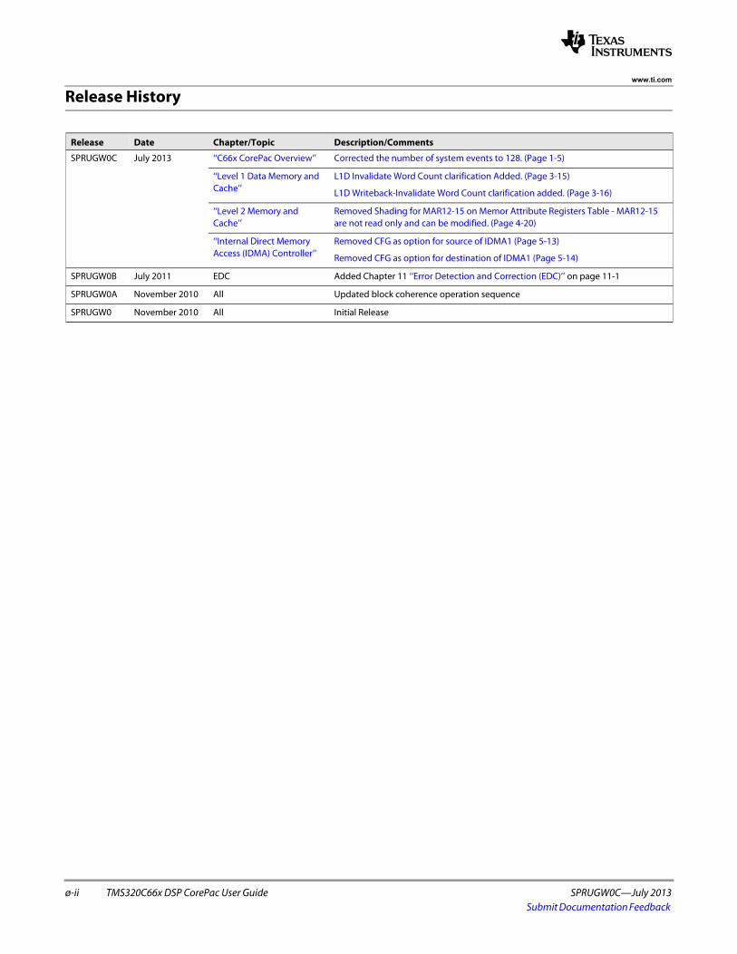
Release History
Release Date Chapter/Topic Description/Comments
SPRUGW0C July 2013 ‘‘C66x CorePac Overview’’ Corrected the number of system events to 128. (Page 1-5)
‘‘Level 1 Data Memory and Cache’’
L1D Invalidate Word Count clarification Added. (Page 3-15)
L1D Writeback-Invalidate Word Count clarification added. (Page 3-16)
‘‘Level 2 Memory and Cache’’
Removed Shading for MAR12-15 on Memor Attribute Registers Table - MAR12-15 are not read only and can be modified. (Page 4-20)
‘‘Internal Direct Memory Access (IDMA) Controller’’
Removed CFG as option for source of IDMA1 (Page 5-13)
Removed CFG as option for destination of IDMA1 (Page 5-14)
SPRUGW0B July 2011 EDC Added Chapter 11 ‘‘Error Detection and Correction (EDC)’’ on page 11-1
SPRUGW0A November 2010 All Updated block coherence operation sequence
SPRUGW0 November 2010 All Initial Release
Contents
SPRUGW0C—July 2013 TMS320C66x DSP CorePac User Guide ø-iiiSubmit Documentation Feedback
www.ti.com
ContentsRelease History. . . . . . . . . . . . . . . . . . . . . . . . . . . . . . . . . . . . . . . . . . . . . . . . . . . . . . . . . . . . . . . . . . . . . . . . . . . . . . . . . . . . . . . . . . . . . . . . . . . . . . . ø-iiList of Tables . . . . . . . . . . . . . . . . . . . . . . . . . . . . . . . . . . . . . . . . . . . . . . . . . . . . . . . . . . . . . . . . . . . . . . . . . . . . . . . . . . . . . . . . . . . . . . . . . . . . . . . . . .ø-xList of Figures . . . . . . . . . . . . . . . . . . . . . . . . . . . . . . . . . . . . . . . . . . . . . . . . . . . . . . . . . . . . . . . . . . . . . . . . . . . . . . . . . . . . . . . . . . . . . . . . . . . . . . . ø-xivList of Examples. . . . . . . . . . . . . . . . . . . . . . . . . . . . . . . . . . . . . . . . . . . . . . . . . . . . . . . . . . . . . . . . . . . . . . . . . . . . . . . . . . . . . . . . . . . . . . . . . . . .ø-xviii
Preface ø-xixAbout This Manual . . . . . . . . . . . . . . . . . . . . . . . . . . . . . . . . . . . . . . . . . . . . . . . . . . . . . . . . . . . . . . . . . . . . . . . . . . . . . . . ø-xixNotational Conventions . . . . . . . . . . . . . . . . . . . . . . . . . . . . . . . . . . . . . . . . . . . . . . . . . . . . . . . . . . . . . . . . . . . . . . . . . . ø-xixRelated Documentation from Texas Instruments . . . . . . . . . . . . . . . . . . . . . . . . . . . . . . . . . . . . . . . . . . . . . . . . . . . ø-xxTrademarks . . . . . . . . . . . . . . . . . . . . . . . . . . . . . . . . . . . . . . . . . . . . . . . . . . . . . . . . . . . . . . . . . . . . . . . . . . . . . . . . . . . . . . . ø-xx
Chapter 1
C66x CorePac Overview 1-11.1 Introduction . . . . . . . . . . . . . . . . . . . . . . . . . . . . . . . . . . . . . . . . . . . . . . . . . . . . . . . . . . . . . . . . . . . . . . . . . . . . . . . . . . . 1-21.2 C66x CorePac Overview . . . . . . . . . . . . . . . . . . . . . . . . . . . . . . . . . . . . . . . . . . . . . . . . . . . . . . . . . . . . . . . . . . . . . . . . 1-3
1.2.1 C66x DSP . . . . . . . . . . . . . . . . . . . . . . . . . . . . . . . . . . . . . . . . . . . . . . . . . . . . . . . . . . . . . . . . . . . . . . . . . . . . . . . . . . . . . . . . . . . 1-31.2.2 Level 1 Program (L1P) Memory Controller. . . . . . . . . . . . . . . . . . . . . . . . . . . . . . . . . . . . . . . . . . . . . . . . . . . . . . . . . . . . 1-31.2.3 Level 1 Data (L1D) Memory Controller . . . . . . . . . . . . . . . . . . . . . . . . . . . . . . . . . . . . . . . . . . . . . . . . . . . . . . . . . . . . . . . 1-31.2.4 Level 2 (L2) Memory Controller . . . . . . . . . . . . . . . . . . . . . . . . . . . . . . . . . . . . . . . . . . . . . . . . . . . . . . . . . . . . . . . . . . . . . . 1-31.2.5 Internal DMA (IDMA) . . . . . . . . . . . . . . . . . . . . . . . . . . . . . . . . . . . . . . . . . . . . . . . . . . . . . . . . . . . . . . . . . . . . . . . . . . . . . . . . 1-41.2.6 External Memory Controller (EMC) . . . . . . . . . . . . . . . . . . . . . . . . . . . . . . . . . . . . . . . . . . . . . . . . . . . . . . . . . . . . . . . . . . . 1-41.2.7 Extended Memory Controller (XMC) . . . . . . . . . . . . . . . . . . . . . . . . . . . . . . . . . . . . . . . . . . . . . . . . . . . . . . . . . . . . . . . . . 1-41.2.8 Bandwidth Management (BWM). . . . . . . . . . . . . . . . . . . . . . . . . . . . . . . . . . . . . . . . . . . . . . . . . . . . . . . . . . . . . . . . . . . . . 1-51.2.9 Interrupt Controller (INTC). . . . . . . . . . . . . . . . . . . . . . . . . . . . . . . . . . . . . . . . . . . . . . . . . . . . . . . . . . . . . . . . . . . . . . . . . . . 1-51.2.10 Memory Protection Architecture (MPA) . . . . . . . . . . . . . . . . . . . . . . . . . . . . . . . . . . . . . . . . . . . . . . . . . . . . . . . . . . . . . 1-61.2.11 Power-Down Controller (PDC). . . . . . . . . . . . . . . . . . . . . . . . . . . . . . . . . . . . . . . . . . . . . . . . . . . . . . . . . . . . . . . . . . . . . . 1-6
Chapter 2
Level 1 Program Memory and Cache 2-12.1 Introduction . . . . . . . . . . . . . . . . . . . . . . . . . . . . . . . . . . . . . . . . . . . . . . . . . . . . . . . . . . . . . . . . . . . . . . . . . . . . . . . . . . . 2-2
2.1.1 Purpose of the Level 1 Program (L1P) Memory and Cache . . . . . . . . . . . . . . . . . . . . . . . . . . . . . . . . . . . . . . . . . . . . 2-22.1.2 Features . . . . . . . . . . . . . . . . . . . . . . . . . . . . . . . . . . . . . . . . . . . . . . . . . . . . . . . . . . . . . . . . . . . . . . . . . . . . . . . . . . . . . . . . . . . . 2-22.1.3 Terms and Definitions . . . . . . . . . . . . . . . . . . . . . . . . . . . . . . . . . . . . . . . . . . . . . . . . . . . . . . . . . . . . . . . . . . . . . . . . . . . . . . . 2-2
2.2 L1 Program Memory Architecture . . . . . . . . . . . . . . . . . . . . . . . . . . . . . . . . . . . . . . . . . . . . . . . . . . . . . . . . . . . . . . 2-22.2.1 L1P Memory . . . . . . . . . . . . . . . . . . . . . . . . . . . . . . . . . . . . . . . . . . . . . . . . . . . . . . . . . . . . . . . . . . . . . . . . . . . . . . . . . . . . . . . . 2-2
2.2.1.1 L1P Access . . . . . . . . . . . . . . . . . . . . . . . . . . . . . . . . . . . . . . . . . . . . . . . . . . . . . . . . . . . . . . . . . . . . . . . . . . . . . . . . . . . 2-22.2.1.2 L1P Wait States . . . . . . . . . . . . . . . . . . . . . . . . . . . . . . . . . . . . . . . . . . . . . . . . . . . . . . . . . . . . . . . . . . . . . . . . . . . . . . . 2-2
2.3 L1P Cache . . . . . . . . . . . . . . . . . . . . . . . . . . . . . . . . . . . . . . . . . . . . . . . . . . . . . . . . . . . . . . . . . . . . . . . . . . . . . . . . . . . . . 2-32.3.1 L1P Cache Architecture. . . . . . . . . . . . . . . . . . . . . . . . . . . . . . . . . . . . . . . . . . . . . . . . . . . . . . . . . . . . . . . . . . . . . . . . . . . . . . 2-32.3.2 Replacement and Allocation Strategy . . . . . . . . . . . . . . . . . . . . . . . . . . . . . . . . . . . . . . . . . . . . . . . . . . . . . . . . . . . . . . . 2-42.3.3 L1P Mode Change Operations . . . . . . . . . . . . . . . . . . . . . . . . . . . . . . . . . . . . . . . . . . . . . . . . . . . . . . . . . . . . . . . . . . . . . . . 2-42.3.4 L1P Freeze Mode . . . . . . . . . . . . . . . . . . . . . . . . . . . . . . . . . . . . . . . . . . . . . . . . . . . . . . . . . . . . . . . . . . . . . . . . . . . . . . . . . . . 2-5
2.4 Program Initiated Coherence Operations . . . . . . . . . . . . . . . . . . . . . . . . . . . . . . . . . . . . . . . . . . . . . . . . . . . . . . . 2-72.4.1 Global Coherence Operation . . . . . . . . . . . . . . . . . . . . . . . . . . . . . . . . . . . . . . . . . . . . . . . . . . . . . . . . . . . . . . . . . . . . . . . . 2-72.4.2 Block Coherence Operation . . . . . . . . . . . . . . . . . . . . . . . . . . . . . . . . . . . . . . . . . . . . . . . . . . . . . . . . . . . . . . . . . . . . . . . . . 2-7
2.5 L1P Cache Control Registers. . . . . . . . . . . . . . . . . . . . . . . . . . . . . . . . . . . . . . . . . . . . . . . . . . . . . . . . . . . . . . . . . . . . 2-92.5.1 Memory Mapped Cache Control Register Overview . . . . . . . . . . . . . . . . . . . . . . . . . . . . . . . . . . . . . . . . . . . . . . . . . . 2-92.5.2 L1P Cache Configuration Registers . . . . . . . . . . . . . . . . . . . . . . . . . . . . . . . . . . . . . . . . . . . . . . . . . . . . . . . . . . . . . . . . . . 2-9
2.5.2.1 L1P Configuration Register (L1PCFG) . . . . . . . . . . . . . . . . . . . . . . . . . . . . . . . . . . . . . . . . . . . . . . . . . . . . . . . . . . 2-92.5.2.2 L1P Cache Control Register (L1PCC) . . . . . . . . . . . . . . . . . . . . . . . . . . . . . . . . . . . . . . . . . . . . . . . . . . . . . . . . . .2-102.5.2.3 L1P Invalidate Base Address Register (L1PIBAR) . . . . . . . . . . . . . . . . . . . . . . . . . . . . . . . . . . . . . . . . . . . . . .2-10
Contents
ø-iv TMS320C66x DSP CorePac User Guide SPRUGW0C—July 2013Submit Documentation Feedback
www.ti.com
2.5.2.4 L1P Invalidate Word Count (L1PIWC) . . . . . . . . . . . . . . . . . . . . . . . . . . . . . . . . . . . . . . . . . . . . . . . . . . . . . . . . .2-112.5.2.5 L1P Invalidate Register (L1PINV). . . . . . . . . . . . . . . . . . . . . . . . . . . . . . . . . . . . . . . . . . . . . . . . . . . . . . . . . . . . . .2-11
2.5.3 Privilege and Cache Control Operations . . . . . . . . . . . . . . . . . . . . . . . . . . . . . . . . . . . . . . . . . . . . . . . . . . . . . . . . . . . .2-122.6 L1P Performance. . . . . . . . . . . . . . . . . . . . . . . . . . . . . . . . . . . . . . . . . . . . . . . . . . . . . . . . . . . . . . . . . . . . . . . . . . . . . .2-13
2.6.1 L1P Miss Penalty . . . . . . . . . . . . . . . . . . . . . . . . . . . . . . . . . . . . . . . . . . . . . . . . . . . . . . . . . . . . . . . . . . . . . . . . . . . . . . . . . . .2-132.6.2 L1P Miss Pipelining . . . . . . . . . . . . . . . . . . . . . . . . . . . . . . . . . . . . . . . . . . . . . . . . . . . . . . . . . . . . . . . . . . . . . . . . . . . . . . . .2-13
2.7 L1P Power-Down Support . . . . . . . . . . . . . . . . . . . . . . . . . . . . . . . . . . . . . . . . . . . . . . . . . . . . . . . . . . . . . . . . . . . . .2-152.7.1 Static Power-Down. . . . . . . . . . . . . . . . . . . . . . . . . . . . . . . . . . . . . . . . . . . . . . . . . . . . . . . . . . . . . . . . . . . . . . . . . . . . . . . . .2-152.7.2 Dynamic Power-Down . . . . . . . . . . . . . . . . . . . . . . . . . . . . . . . . . . . . . . . . . . . . . . . . . . . . . . . . . . . . . . . . . . . . . . . . . . . . .2-152.7.3 Feature-Oriented Power-Down . . . . . . . . . . . . . . . . . . . . . . . . . . . . . . . . . . . . . . . . . . . . . . . . . . . . . . . . . . . . . . . . . . . . .2-15
2.8 L1P Memory Protection . . . . . . . . . . . . . . . . . . . . . . . . . . . . . . . . . . . . . . . . . . . . . . . . . . . . . . . . . . . . . . . . . . . . . . .2-162.8.1 Protection Checks on L1P Accesses . . . . . . . . . . . . . . . . . . . . . . . . . . . . . . . . . . . . . . . . . . . . . . . . . . . . . . . . . . . . . . . . .2-16
2.8.1.1 Protection Checks on DSP Program Fetches . . . . . . . . . . . . . . . . . . . . . . . . . . . . . . . . . . . . . . . . . . . . . . . . . .2-162.8.1.2 Protection Checks on DSP Data Accesses . . . . . . . . . . . . . . . . . . . . . . . . . . . . . . . . . . . . . . . . . . . . . . . . . . . . .2-162.8.1.3 Protection Checks on DMA/IDMA Accesses . . . . . . . . . . . . . . . . . . . . . . . . . . . . . . . . . . . . . . . . . . . . . . . . . .2-16
2.8.2 Memory Protection Registers . . . . . . . . . . . . . . . . . . . . . . . . . . . . . . . . . . . . . . . . . . . . . . . . . . . . . . . . . . . . . . . . . . . . . . .2-172.8.2.1 Memory Page Protection Attribute Registers . . . . . . . . . . . . . . . . . . . . . . . . . . . . . . . . . . . . . . . . . . . . . . . . .2-172.8.2.2 Memory Protection Lock Registers . . . . . . . . . . . . . . . . . . . . . . . . . . . . . . . . . . . . . . . . . . . . . . . . . . . . . . . . . . .2-192.8.2.3 Memory Protection Fault Registers . . . . . . . . . . . . . . . . . . . . . . . . . . . . . . . . . . . . . . . . . . . . . . . . . . . . . . . . . . .2-20
Chapter 3
Level 1 Data Memory and Cache 3-13.1 Introduction . . . . . . . . . . . . . . . . . . . . . . . . . . . . . . . . . . . . . . . . . . . . . . . . . . . . . . . . . . . . . . . . . . . . . . . . . . . . . . . . . . . 3-2
3.1.1 Purpose of the Level 1 Data (L1D) Memory and Cache . . . . . . . . . . . . . . . . . . . . . . . . . . . . . . . . . . . . . . . . . . . . . . . . 3-23.1.2 Features . . . . . . . . . . . . . . . . . . . . . . . . . . . . . . . . . . . . . . . . . . . . . . . . . . . . . . . . . . . . . . . . . . . . . . . . . . . . . . . . . . . . . . . . . . . . 3-23.1.3 Terms and Definitions . . . . . . . . . . . . . . . . . . . . . . . . . . . . . . . . . . . . . . . . . . . . . . . . . . . . . . . . . . . . . . . . . . . . . . . . . . . . . . . 3-2
3.2 L1D Memory Architecture . . . . . . . . . . . . . . . . . . . . . . . . . . . . . . . . . . . . . . . . . . . . . . . . . . . . . . . . . . . . . . . . . . . . . . 3-23.2.1 L1D Memory . . . . . . . . . . . . . . . . . . . . . . . . . . . . . . . . . . . . . . . . . . . . . . . . . . . . . . . . . . . . . . . . . . . . . . . . . . . . . . . . . . . . . . . . 3-2
3.3 L1D Cache . . . . . . . . . . . . . . . . . . . . . . . . . . . . . . . . . . . . . . . . . . . . . . . . . . . . . . . . . . . . . . . . . . . . . . . . . . . . . . . . . . . . . 3-23.3.1 L1D Cache Architecture . . . . . . . . . . . . . . . . . . . . . . . . . . . . . . . . . . . . . . . . . . . . . . . . . . . . . . . . . . . . . . . . . . . . . . . . . . . . . 3-33.3.2 Replacement and Allocation Strategy . . . . . . . . . . . . . . . . . . . . . . . . . . . . . . . . . . . . . . . . . . . . . . . . . . . . . . . . . . . . . . . 3-43.3.3 L1D Mode Change Operations. . . . . . . . . . . . . . . . . . . . . . . . . . . . . . . . . . . . . . . . . . . . . . . . . . . . . . . . . . . . . . . . . . . . . . . 3-43.3.4 L1D Freeze Mode . . . . . . . . . . . . . . . . . . . . . . . . . . . . . . . . . . . . . . . . . . . . . . . . . . . . . . . . . . . . . . . . . . . . . . . . . . . . . . . . . . . 3-53.3.5 Program-Initiated Cache Coherence Operations . . . . . . . . . . . . . . . . . . . . . . . . . . . . . . . . . . . . . . . . . . . . . . . . . . . . . 3-8
3.3.5.1 Global Coherence Operations . . . . . . . . . . . . . . . . . . . . . . . . . . . . . . . . . . . . . . . . . . . . . . . . . . . . . . . . . . . . . . . . . 3-83.3.5.2 Block Coherence Operations . . . . . . . . . . . . . . . . . . . . . . . . . . . . . . . . . . . . . . . . . . . . . . . . . . . . . . . . . . . . . . . . . . 3-9
3.3.6 Cache Coherence Protocol . . . . . . . . . . . . . . . . . . . . . . . . . . . . . . . . . . . . . . . . . . . . . . . . . . . . . . . . . . . . . . . . . . . . . . . . .3-103.3.6.1 L2 to L1D Cache Coherence Protocol . . . . . . . . . . . . . . . . . . . . . . . . . . . . . . . . . . . . . . . . . . . . . . . . . . . . . . . .3-113.3.6.2 L1D to L2 Cache Coherence Protocol . . . . . . . . . . . . . . . . . . . . . . . . . . . . . . . . . . . . . . . . . . . . . . . . . . . . . . . .3-11
3.4 L1D Cache Control Registers . . . . . . . . . . . . . . . . . . . . . . . . . . . . . . . . . . . . . . . . . . . . . . . . . . . . . . . . . . . . . . . . . .3-123.4.1 Memory Mapped L1D Cache Control Register Overview . . . . . . . . . . . . . . . . . . . . . . . . . . . . . . . . . . . . . . . . . . . . .3-123.4.2 L1D Cache Configuration Registers . . . . . . . . . . . . . . . . . . . . . . . . . . . . . . . . . . . . . . . . . . . . . . . . . . . . . . . . . . . . . . . . .3-12
3.4.2.1 L1D Cache Configuration (L1DCFG) Register. . . . . . . . . . . . . . . . . . . . . . . . . . . . . . . . . . . . . . . . . . . . . . . . . .3-123.4.2.2 L1D Cache Control (L1DCC) Register . . . . . . . . . . . . . . . . . . . . . . . . . . . . . . . . . . . . . . . . . . . . . . . . . . . . . . . . .3-13
3.4.3 L1D Cache Coherence Operation Registers. . . . . . . . . . . . . . . . . . . . . . . . . . . . . . . . . . . . . . . . . . . . . . . . . . . . . . . . . .3-143.4.3.1 Global Coherence Operation Registers . . . . . . . . . . . . . . . . . . . . . . . . . . . . . . . . . . . . . . . . . . . . . . . . . . . . . . .3-143.4.3.2 Block Coherence Operation Registers . . . . . . . . . . . . . . . . . . . . . . . . . . . . . . . . . . . . . . . . . . . . . . . . . . . . . . . .3-15
3.4.4 Privilege and Cache Control Operations . . . . . . . . . . . . . . . . . . . . . . . . . . . . . . . . . . . . . . . . . . . . . . . . . . . . . . . . . . . .3-163.5 L1D Memory Performance . . . . . . . . . . . . . . . . . . . . . . . . . . . . . . . . . . . . . . . . . . . . . . . . . . . . . . . . . . . . . . . . . . . .3-18
3.5.1 L1D Memory Banking . . . . . . . . . . . . . . . . . . . . . . . . . . . . . . . . . . . . . . . . . . . . . . . . . . . . . . . . . . . . . . . . . . . . . . . . . . . . . .3-183.5.2 L1D Miss Penalty . . . . . . . . . . . . . . . . . . . . . . . . . . . . . . . . . . . . . . . . . . . . . . . . . . . . . . . . . . . . . . . . . . . . . . . . . . . . . . . . . . .3-193.5.3 L1D Write Buffer . . . . . . . . . . . . . . . . . . . . . . . . . . . . . . . . . . . . . . . . . . . . . . . . . . . . . . . . . . . . . . . . . . . . . . . . . . . . . . . . . . .3-203.5.4 L1D Miss Pipelining . . . . . . . . . . . . . . . . . . . . . . . . . . . . . . . . . . . . . . . . . . . . . . . . . . . . . . . . . . . . . . . . . . . . . . . . . . . . . . . .3-21
3.6 L1D Power-Down Support . . . . . . . . . . . . . . . . . . . . . . . . . . . . . . . . . . . . . . . . . . . . . . . . . . . . . . . . . . . . . . . . . . . .3-223.7 L1D Memory Protection . . . . . . . . . . . . . . . . . . . . . . . . . . . . . . . . . . . . . . . . . . . . . . . . . . . . . . . . . . . . . . . . . . . . . . .3-23
3.7.1 Protection Checks on L1D Accesses. . . . . . . . . . . . . . . . . . . . . . . . . . . . . . . . . . . . . . . . . . . . . . . . . . . . . . . . . . . . . . . . .3-23

Contents
SPRUGW0C—July 2013 TMS320C66x DSP CorePac User Guide ø-vSubmit Documentation Feedback
www.ti.com
3.7.1.1 Protection Checks on DSP, IDMA and Other System Master Accesses . . . . . . . . . . . . . . . . . . . . . . . . . .3-233.7.1.2 Additional Protection Checks on Program Initiated Cache Coherence Operations. . . . . . . . . . . . . .3-23
3.7.2 L1D Memory Protection Registers . . . . . . . . . . . . . . . . . . . . . . . . . . . . . . . . . . . . . . . . . . . . . . . . . . . . . . . . . . . . . . . . . .3-233.7.2.1 Memory Protection Attribute Registers . . . . . . . . . . . . . . . . . . . . . . . . . . . . . . . . . . . . . . . . . . . . . . . . . . . . . . .3-243.7.2.2 Memory Protection Lock Registers . . . . . . . . . . . . . . . . . . . . . . . . . . . . . . . . . . . . . . . . . . . . . . . . . . . . . . . . . . .3-263.7.2.3 Memory Protection Fault Registers . . . . . . . . . . . . . . . . . . . . . . . . . . . . . . . . . . . . . . . . . . . . . . . . . . . . . . . . . . .3-26
3.7.3 Protection Checks on Accesses to Memory Protection Registers . . . . . . . . . . . . . . . . . . . . . . . . . . . . . . . . . . . . .3-28
Chapter 4
Level 2 Memory and Cache 4-14.1 Introduction . . . . . . . . . . . . . . . . . . . . . . . . . . . . . . . . . . . . . . . . . . . . . . . . . . . . . . . . . . . . . . . . . . . . . . . . . . . . . . . . . . . 4-2
4.1.1 Purpose of the Level 2 (L2) Memory and Cache. . . . . . . . . . . . . . . . . . . . . . . . . . . . . . . . . . . . . . . . . . . . . . . . . . . . . . . 4-24.1.2 Features . . . . . . . . . . . . . . . . . . . . . . . . . . . . . . . . . . . . . . . . . . . . . . . . . . . . . . . . . . . . . . . . . . . . . . . . . . . . . . . . . . . . . . . . . . . . 4-24.1.3 Terms and Definitions . . . . . . . . . . . . . . . . . . . . . . . . . . . . . . . . . . . . . . . . . . . . . . . . . . . . . . . . . . . . . . . . . . . . . . . . . . . . . . . 4-2
4.2 Level 2 Memory Architecture . . . . . . . . . . . . . . . . . . . . . . . . . . . . . . . . . . . . . . . . . . . . . . . . . . . . . . . . . . . . . . . . . . . 4-34.2.1 L2 Memory . . . . . . . . . . . . . . . . . . . . . . . . . . . . . . . . . . . . . . . . . . . . . . . . . . . . . . . . . . . . . . . . . . . . . . . . . . . . . . . . . . . . . . . . . 4-3
4.2.1.1 L2 Memory Port . . . . . . . . . . . . . . . . . . . . . . . . . . . . . . . . . . . . . . . . . . . . . . . . . . . . . . . . . . . . . . . . . . . . . . . . . . . . . . 4-34.2.1.2 L2 Memory Sizes . . . . . . . . . . . . . . . . . . . . . . . . . . . . . . . . . . . . . . . . . . . . . . . . . . . . . . . . . . . . . . . . . . . . . . . . . . . . . 4-34.2.1.3 Level 2 Memory Architecture L2 Memory Banking . . . . . . . . . . . . . . . . . . . . . . . . . . . . . . . . . . . . . . . . . . . . . 4-34.2.1.4 Simultaneous Accesses to L2 Memory . . . . . . . . . . . . . . . . . . . . . . . . . . . . . . . . . . . . . . . . . . . . . . . . . . . . . . . . 4-4
4.3 L2 Cache . . . . . . . . . . . . . . . . . . . . . . . . . . . . . . . . . . . . . . . . . . . . . . . . . . . . . . . . . . . . . . . . . . . . . . . . . . . . . . . . . . . . . . 4-44.3.1 L2 Cache Architecture . . . . . . . . . . . . . . . . . . . . . . . . . . . . . . . . . . . . . . . . . . . . . . . . . . . . . . . . . . . . . . . . . . . . . . . . . . . . . . 4-44.3.2 Replacement and Allocation Strategy . . . . . . . . . . . . . . . . . . . . . . . . . . . . . . . . . . . . . . . . . . . . . . . . . . . . . . . . . . . . . . . 4-54.3.3 Reset Behavior . . . . . . . . . . . . . . . . . . . . . . . . . . . . . . . . . . . . . . . . . . . . . . . . . . . . . . . . . . . . . . . . . . . . . . . . . . . . . . . . . . . . . . 4-54.3.4 L2 Mode Change Operations . . . . . . . . . . . . . . . . . . . . . . . . . . . . . . . . . . . . . . . . . . . . . . . . . . . . . . . . . . . . . . . . . . . . . . . . 4-64.3.5 L2 Freeze Mode . . . . . . . . . . . . . . . . . . . . . . . . . . . . . . . . . . . . . . . . . . . . . . . . . . . . . . . . . . . . . . . . . . . . . . . . . . . . . . . . . . . . . 4-74.3.6 Program Initiated Cache Coherence Operations. . . . . . . . . . . . . . . . . . . . . . . . . . . . . . . . . . . . . . . . . . . . . . . . . . . . . . 4-7
4.3.6.1 Global Coherence Operations . . . . . . . . . . . . . . . . . . . . . . . . . . . . . . . . . . . . . . . . . . . . . . . . . . . . . . . . . . . . . . . . 4-84.3.6.2 Block Coherence Operations . . . . . . . . . . . . . . . . . . . . . . . . . . . . . . . . . . . . . . . . . . . . . . . . . . . . . . . . . . . . . . . . . . 4-8
4.3.7 Cacheability Controls . . . . . . . . . . . . . . . . . . . . . . . . . . . . . . . . . . . . . . . . . . . . . . . . . . . . . . . . . . . . . . . . . . . . . . . . . . . . . .4-104.3.7.1 MAR Functions . . . . . . . . . . . . . . . . . . . . . . . . . . . . . . . . . . . . . . . . . . . . . . . . . . . . . . . . . . . . . . . . . . . . . . . . . . . . . .4-104.3.7.2 Special MAR Registers . . . . . . . . . . . . . . . . . . . . . . . . . . . . . . . . . . . . . . . . . . . . . . . . . . . . . . . . . . . . . . . . . . . . . . .4-104.3.7.3 Requirements for updating MAR registers at runtime . . . . . . . . . . . . . . . . . . . . . . . . . . . . . . . . . . . . . . . . .4-114.3.7.4 L1 Interaction . . . . . . . . . . . . . . . . . . . . . . . . . . . . . . . . . . . . . . . . . . . . . . . . . . . . . . . . . . . . . . . . . . . . . . . . . . . . . . .4-11
4.3.8 L1-L2 Coherence Support . . . . . . . . . . . . . . . . . . . . . . . . . . . . . . . . . . . . . . . . . . . . . . . . . . . . . . . . . . . . . . . . . . . . . . . . . .4-114.3.8.1 Cache Coherence Protocol . . . . . . . . . . . . . . . . . . . . . . . . . . . . . . . . . . . . . . . . . . . . . . . . . . . . . . . . . . . . . . . . . . .4-124.3.8.2 L2 Cache Evictions . . . . . . . . . . . . . . . . . . . . . . . . . . . . . . . . . . . . . . . . . . . . . . . . . . . . . . . . . . . . . . . . . . . . . . . . . .4-124.3.8.3 Policy Relative to L1D Victims . . . . . . . . . . . . . . . . . . . . . . . . . . . . . . . . . . . . . . . . . . . . . . . . . . . . . . . . . . . . . . .4-124.3.8.4 DMA/IDMA Write Interaction . . . . . . . . . . . . . . . . . . . . . . . . . . . . . . . . . . . . . . . . . . . . . . . . . . . . . . . . . . . . . . . .4-134.3.8.5 DMA/IDMA Read Interaction . . . . . . . . . . . . . . . . . . . . . . . . . . . . . . . . . . . . . . . . . . . . . . . . . . . . . . . . . . . . . . . . .4-13
4.4 L2 Cache Control Registers . . . . . . . . . . . . . . . . . . . . . . . . . . . . . . . . . . . . . . . . . . . . . . . . . . . . . . . . . . . . . . . . . . . .4-144.4.1 Memory Mapped L2 Cache Control Registers Overview. . . . . . . . . . . . . . . . . . . . . . . . . . . . . . . . . . . . . . . . . . . . . .4-144.4.2 L2 Configuration Register (L2CFG) . . . . . . . . . . . . . . . . . . . . . . . . . . . . . . . . . . . . . . . . . . . . . . . . . . . . . . . . . . . . . . . . . .4-144.4.3 L2 Cache Coherence Operation Registers . . . . . . . . . . . . . . . . . . . . . . . . . . . . . . . . . . . . . . . . . . . . . . . . . . . . . . . . . . .4-15
4.4.3.1 Block Coherence Operation Registers . . . . . . . . . . . . . . . . . . . . . . . . . . . . . . . . . . . . . . . . . . . . . . . . . . . . . . . .4-154.4.3.2 Global Coherence Operation Registers . . . . . . . . . . . . . . . . . . . . . . . . . . . . . . . . . . . . . . . . . . . . . . . . . . . . . . .4-18
4.4.4 Memory Attribute Registers (MARn) . . . . . . . . . . . . . . . . . . . . . . . . . . . . . . . . . . . . . . . . . . . . . . . . . . . . . . . . . . . . . . . .4-194.4.5 Memory Attribute Register (MARn) Definition . . . . . . . . . . . . . . . . . . . . . . . . . . . . . . . . . . . . . . . . . . . . . . . . . . . . . . .4-264.4.6 XMC Prefetch Support . . . . . . . . . . . . . . . . . . . . . . . . . . . . . . . . . . . . . . . . . . . . . . . . . . . . . . . . . . . . . . . . . . . . . . . . . . . . .4-264.4.7 Privilege and Cache Control Registers. . . . . . . . . . . . . . . . . . . . . . . . . . . . . . . . . . . . . . . . . . . . . . . . . . . . . . . . . . . . . . .4-27
4.5 L2 Power-Down. . . . . . . . . . . . . . . . . . . . . . . . . . . . . . . . . . . . . . . . . . . . . . . . . . . . . . . . . . . . . . . . . . . . . . . . . . . . . . .4-284.5.1 L2 Memory Static Power-Down . . . . . . . . . . . . . . . . . . . . . . . . . . . . . . . . . . . . . . . . . . . . . . . . . . . . . . . . . . . . . . . . . . . .4-284.5.2 L2 Memory Dynamic Power-Down . . . . . . . . . . . . . . . . . . . . . . . . . . . . . . . . . . . . . . . . . . . . . . . . . . . . . . . . . . . . . . . . .4-28
4.6 L2 Memory Protection . . . . . . . . . . . . . . . . . . . . . . . . . . . . . . . . . . . . . . . . . . . . . . . . . . . . . . . . . . . . . . . . . . . . . . . .4-294.6.1 Protection Checks on DSP, IDMA and Other System Master Accesses. . . . . . . . . . . . . . . . . . . . . . . . . . . . . . . . .4-294.6.2 L2 Memory Protection Registers . . . . . . . . . . . . . . . . . . . . . . . . . . . . . . . . . . . . . . . . . . . . . . . . . . . . . . . . . . . . . . . . . . . .4-29
4.6.2.1 L2 Memory Protection Registers . . . . . . . . . . . . . . . . . . . . . . . . . . . . . . . . . . . . . . . . . . . . . . . . . . . . . . . . . . . . .4-30
Contents
ø-vi TMS320C66x DSP CorePac User Guide SPRUGW0C—July 2013Submit Documentation Feedback
www.ti.com
4.6.2.2 Memory Protection Page Attribute Registers (L2MPPAxx) . . . . . . . . . . . . . . . . . . . . . . . . . . . . . . . . . . . . .4-304.6.2.3 Memory Protection Lock Registers . . . . . . . . . . . . . . . . . . . . . . . . . . . . . . . . . . . . . . . . . . . . . . . . . . . . . . . . . . .4-324.6.2.4 Memory Protection Fault Registers . . . . . . . . . . . . . . . . . . . . . . . . . . . . . . . . . . . . . . . . . . . . . . . . . . . . . . . . . . .4-33
4.6.3 Protection Checks on Accesses to Memory Protection Registers . . . . . . . . . . . . . . . . . . . . . . . . . . . . . . . . . . . . .4-354.7 MDMA Bus Error Reporting. . . . . . . . . . . . . . . . . . . . . . . . . . . . . . . . . . . . . . . . . . . . . . . . . . . . . . . . . . . . . . . . . . . .4-36
4.7.1 MDMA Bus Error Register (MDMAERR) . . . . . . . . . . . . . . . . . . . . . . . . . . . . . . . . . . . . . . . . . . . . . . . . . . . . . . . . . . . . . .4-364.7.2 MDMA Bus Error Clear Register (MDMAERRCLR) . . . . . . . . . . . . . . . . . . . . . . . . . . . . . . . . . . . . . . . . . . . . . . . . . . . . .4-37
Chapter 5
Internal Direct Memory Access (IDMA) Controller 5-15.1 Introduction . . . . . . . . . . . . . . . . . . . . . . . . . . . . . . . . . . . . . . . . . . . . . . . . . . . . . . . . . . . . . . . . . . . . . . . . . . . . . . . . . . . 5-2
5.1.1 Purpose of the Internal Direct Memory Access (IDMA) Controller . . . . . . . . . . . . . . . . . . . . . . . . . . . . . . . . . . . . . 5-25.1.2 Features . . . . . . . . . . . . . . . . . . . . . . . . . . . . . . . . . . . . . . . . . . . . . . . . . . . . . . . . . . . . . . . . . . . . . . . . . . . . . . . . . . . . . . . . . . . . 5-2
5.2 Terms and Definitions. . . . . . . . . . . . . . . . . . . . . . . . . . . . . . . . . . . . . . . . . . . . . . . . . . . . . . . . . . . . . . . . . . . . . . . . . . 5-35.3 IDMA Architecture . . . . . . . . . . . . . . . . . . . . . . . . . . . . . . . . . . . . . . . . . . . . . . . . . . . . . . . . . . . . . . . . . . . . . . . . . . . . . 5-3
5.3.1 IDMA Channel 0 . . . . . . . . . . . . . . . . . . . . . . . . . . . . . . . . . . . . . . . . . . . . . . . . . . . . . . . . . . . . . . . . . . . . . . . . . . . . . . . . . . . . 5-35.3.1.1 IDMA Channel 0 Operation . . . . . . . . . . . . . . . . . . . . . . . . . . . . . . . . . . . . . . . . . . . . . . . . . . . . . . . . . . . . . . . . . . . 5-35.3.1.2 IDMA Channel 0 Exception. . . . . . . . . . . . . . . . . . . . . . . . . . . . . . . . . . . . . . . . . . . . . . . . . . . . . . . . . . . . . . . . . . . . 5-45.3.1.3 Programming IDMA Channel 0 . . . . . . . . . . . . . . . . . . . . . . . . . . . . . . . . . . . . . . . . . . . . . . . . . . . . . . . . . . . . . . . 5-4
5.3.2 IDMA Channel 1. . . . . . . . . . . . . . . . . . . . . . . . . . . . . . . . . . . . . . . . . . . . . . . . . . . . . . . . . . . . . . . . . . . . . . . . . . . . . . . . . . . . . 5-55.3.2.1 IDMA Channel 1 Operation . . . . . . . . . . . . . . . . . . . . . . . . . . . . . . . . . . . . . . . . . . . . . . . . . . . . . . . . . . . . . . . . . . . 5-55.3.2.2 Programming IDMA Channel 1 . . . . . . . . . . . . . . . . . . . . . . . . . . . . . . . . . . . . . . . . . . . . . . . . . . . . . . . . . . . . . . . . 5-6
5.4 IDMA Registers . . . . . . . . . . . . . . . . . . . . . . . . . . . . . . . . . . . . . . . . . . . . . . . . . . . . . . . . . . . . . . . . . . . . . . . . . . . . . . . . 5-85.4.1 IDMA Channel 0 Status Register (IDMA0_STAT) . . . . . . . . . . . . . . . . . . . . . . . . . . . . . . . . . . . . . . . . . . . . . . . . . . . . . . 5-85.4.2 IDMA Channel 0 Mask Register (IDMA0_MASK). . . . . . . . . . . . . . . . . . . . . . . . . . . . . . . . . . . . . . . . . . . . . . . . . . . . . . . 5-95.4.3 IDMA Channel 0 Source Address Register (IDMA0_SOURCE) . . . . . . . . . . . . . . . . . . . . . . . . . . . . . . . . . . . . . . . . . . 5-95.4.4 IDMA Channel 0 Destination Address Register (IDMA0_DEST) . . . . . . . . . . . . . . . . . . . . . . . . . . . . . . . . . . . . . . .5-105.4.5 IDMA Channel 0 Count Register (IDMA0_COUNT) . . . . . . . . . . . . . . . . . . . . . . . . . . . . . . . . . . . . . . . . . . . . . . . . . . .5-115.4.6 IDMA Channel 1 Status Register (IDMA1_STAT) . . . . . . . . . . . . . . . . . . . . . . . . . . . . . . . . . . . . . . . . . . . . . . . . . . . . .5-125.4.7 IDMA Channel 1 Source Address Register (IDMA1_SOURCE) . . . . . . . . . . . . . . . . . . . . . . . . . . . . . . . . . . . . . . . . .5-125.4.8 IDMA Channel 1 Destination Address Register (IDMA1_DEST) . . . . . . . . . . . . . . . . . . . . . . . . . . . . . . . . . . . . . . .5-135.4.9 IDMA Channel 1 Count Register (IDMA1_COUNT) . . . . . . . . . . . . . . . . . . . . . . . . . . . . . . . . . . . . . . . . . . . . . . . . . . .5-14
5.5 Privilege Levels and IDMA Operation . . . . . . . . . . . . . . . . . . . . . . . . . . . . . . . . . . . . . . . . . . . . . . . . . . . . . . . . . .5-15
Chapter 6
External Memory Controller (EMC) 6-16.1 Introduction . . . . . . . . . . . . . . . . . . . . . . . . . . . . . . . . . . . . . . . . . . . . . . . . . . . . . . . . . . . . . . . . . . . . . . . . . . . . . . . . . . . 6-26.2 PrivID to AID Remap Table . . . . . . . . . . . . . . . . . . . . . . . . . . . . . . . . . . . . . . . . . . . . . . . . . . . . . . . . . . . . . . . . . . . . . 6-26.3 PrivID to AID Mapping . . . . . . . . . . . . . . . . . . . . . . . . . . . . . . . . . . . . . . . . . . . . . . . . . . . . . . . . . . . . . . . . . . . . . . . . . 6-36.4 CFG Bus Error Reporting. . . . . . . . . . . . . . . . . . . . . . . . . . . . . . . . . . . . . . . . . . . . . . . . . . . . . . . . . . . . . . . . . . . . . . . . 6-3
6.4.1 CFG Bus Error Register (ECFGERR). . . . . . . . . . . . . . . . . . . . . . . . . . . . . . . . . . . . . . . . . . . . . . . . . . . . . . . . . . . . . . . . . . . . 6-36.4.2 CFG Bus Error Clear Register (ECFGERRCLR) . . . . . . . . . . . . . . . . . . . . . . . . . . . . . . . . . . . . . . . . . . . . . . . . . . . . . . . . . . 6-4
Chapter 7
Extended Memory Controller (XMC) 7-17.1 Introduction . . . . . . . . . . . . . . . . . . . . . . . . . . . . . . . . . . . . . . . . . . . . . . . . . . . . . . . . . . . . . . . . . . . . . . . . . . . . . . . . . . . 7-27.2 Memory Mapped Register Summary. . . . . . . . . . . . . . . . . . . . . . . . . . . . . . . . . . . . . . . . . . . . . . . . . . . . . . . . . . . . 7-2
7.2.1 XMC Memory Mapped Register Summary. . . . . . . . . . . . . . . . . . . . . . . . . . . . . . . . . . . . . . . . . . . . . . . . . . . . . . . . . . . . 7-27.3 XMC Memory Protection and Address eXtension (MPAX) . . . . . . . . . . . . . . . . . . . . . . . . . . . . . . . . . . . . . . . . 7-5
7.3.1 XMC MPAX Segment Registers . . . . . . . . . . . . . . . . . . . . . . . . . . . . . . . . . . . . . . . . . . . . . . . . . . . . . . . . . . . . . . . . . . . . . . 7-57.3.1.1 Segment Register Layout . . . . . . . . . . . . . . . . . . . . . . . . . . . . . . . . . . . . . . . . . . . . . . . . . . . . . . . . . . . . . . . . . . . . . 7-57.3.1.2 MPAX Segment Register Memory Map . . . . . . . . . . . . . . . . . . . . . . . . . . . . . . . . . . . . . . . . . . . . . . . . . . . . . . . . 7-67.3.1.3 MPAX Register Reset Defaults . . . . . . . . . . . . . . . . . . . . . . . . . . . . . . . . . . . . . . . . . . . . . . . . . . . . . . . . . . . . . . . . . 7-7
7.3.2 Memory Protection and Address Extension Process . . . . . . . . . . . . . . . . . . . . . . . . . . . . . . . . . . . . . . . . . . . . . . . . . . 7-8

Contents
SPRUGW0C—July 2013 TMS320C66x DSP CorePac User Guide ø-viiSubmit Documentation Feedback
www.ti.com
7.3.2.1 Address Range Lookup . . . . . . . . . . . . . . . . . . . . . . . . . . . . . . . . . . . . . . . . . . . . . . . . . . . . . . . . . . . . . . . . . . . . . . . 7-87.3.2.2 Address Extension . . . . . . . . . . . . . . . . . . . . . . . . . . . . . . . . . . . . . . . . . . . . . . . . . . . . . . . . . . . . . . . . . . . . . . . . . . .7-11
7.4 XMC Memory Protection Architecture Support. . . . . . . . . . . . . . . . . . . . . . . . . . . . . . . . . . . . . . . . . . . . . . . . .7-137.4.1 Memory Protection Fault Reporting Registers . . . . . . . . . . . . . . . . . . . . . . . . . . . . . . . . . . . . . . . . . . . . . . . . . . . . . . .7-13
7.5 Prefetch Buffers . . . . . . . . . . . . . . . . . . . . . . . . . . . . . . . . . . . . . . . . . . . . . . . . . . . . . . . . . . . . . . . . . . . . . . . . . . . . . . .7-147.5.1 Data Prefetch Buffer. . . . . . . . . . . . . . . . . . . . . . . . . . . . . . . . . . . . . . . . . . . . . . . . . . . . . . . . . . . . . . . . . . . . . . . . . . . . . . . .7-14
7.5.1.1 Capacity. . . . . . . . . . . . . . . . . . . . . . . . . . . . . . . . . . . . . . . . . . . . . . . . . . . . . . . . . . . . . . . . . . . . . . . . . . . . . . . . . . . . .7-147.5.1.2 Allocation Policy. . . . . . . . . . . . . . . . . . . . . . . . . . . . . . . . . . . . . . . . . . . . . . . . . . . . . . . . . . . . . . . . . . . . . . . . . . . . .7-147.5.1.3 Stream Detection Filter (Candidate Buffer). . . . . . . . . . . . . . . . . . . . . . . . . . . . . . . . . . . . . . . . . . . . . . . . . . . .7-14
7.5.2 Program Prefetch Buffer. . . . . . . . . . . . . . . . . . . . . . . . . . . . . . . . . . . . . . . . . . . . . . . . . . . . . . . . . . . . . . . . . . . . . . . . . . . .7-157.5.2.1 Capacity. . . . . . . . . . . . . . . . . . . . . . . . . . . . . . . . . . . . . . . . . . . . . . . . . . . . . . . . . . . . . . . . . . . . . . . . . . . . . . . . . . . . .7-157.5.2.2 Allocation Policy. . . . . . . . . . . . . . . . . . . . . . . . . . . . . . . . . . . . . . . . . . . . . . . . . . . . . . . . . . . . . . . . . . . . . . . . . . . . .7-15
7.5.3 Prefetch Coherence Issues—Example. . . . . . . . . . . . . . . . . . . . . . . . . . . . . . . . . . . . . . . . . . . . . . . . . . . . . . . . . . . . . . .7-167.6 Prefetch Buffer Memory Mapped Registers . . . . . . . . . . . . . . . . . . . . . . . . . . . . . . . . . . . . . . . . . . . . . . . . . . . .7-17
7.6.1 Prefetch Buffer Command Register: XPFCMD. . . . . . . . . . . . . . . . . . . . . . . . . . . . . . . . . . . . . . . . . . . . . . . . . . . . . . . .7-177.6.2 Prefetch Buffer Performance Analysis Registers . . . . . . . . . . . . . . . . . . . . . . . . . . . . . . . . . . . . . . . . . . . . . . . . . . . . .7-17
7.6.2.1 Analysis Counter Overview . . . . . . . . . . . . . . . . . . . . . . . . . . . . . . . . . . . . . . . . . . . . . . . . . . . . . . . . . . . . . . . . . .7-187.6.2.2 Counting Modes. . . . . . . . . . . . . . . . . . . . . . . . . . . . . . . . . . . . . . . . . . . . . . . . . . . . . . . . . . . . . . . . . . . . . . . . . . . . .7-197.6.2.3 Interpreting Analysis Counters . . . . . . . . . . . . . . . . . . . . . . . . . . . . . . . . . . . . . . . . . . . . . . . . . . . . . . . . . . . . . . .7-19
7.6.3 Data Prefetch Buffer Address Visibility Register: XPFADDR . . . . . . . . . . . . . . . . . . . . . . . . . . . . . . . . . . . . . . . . . . .7-207.6.4 Prefetch Priority Register . . . . . . . . . . . . . . . . . . . . . . . . . . . . . . . . . . . . . . . . . . . . . . . . . . . . . . . . . . . . . . . . . . . . . . . . . . .7-20
Chapter 8
Bandwidth Management Architecture 8-18.1 Introduction . . . . . . . . . . . . . . . . . . . . . . . . . . . . . . . . . . . . . . . . . . . . . . . . . . . . . . . . . . . . . . . . . . . . . . . . . . . . . . . . . . . 8-2
8.1.1 Purpose of the Bandwidth Management . . . . . . . . . . . . . . . . . . . . . . . . . . . . . . . . . . . . . . . . . . . . . . . . . . . . . . . . . . . . . 8-28.1.2 Resource Bandwidth Protected by Bandwidth Management. . . . . . . . . . . . . . . . . . . . . . . . . . . . . . . . . . . . . . . . . . 8-28.1.3 Requestors Managed by Bandwidth Management . . . . . . . . . . . . . . . . . . . . . . . . . . . . . . . . . . . . . . . . . . . . . . . . . . . 8-28.1.4 Terms and Definitions . . . . . . . . . . . . . . . . . . . . . . . . . . . . . . . . . . . . . . . . . . . . . . . . . . . . . . . . . . . . . . . . . . . . . . . . . . . . . . . 8-2
8.2 Bandwidth Management Architecture . . . . . . . . . . . . . . . . . . . . . . . . . . . . . . . . . . . . . . . . . . . . . . . . . . . . . . . . . . 8-38.2.1 Bandwidth Arbitration via Priority Levels. . . . . . . . . . . . . . . . . . . . . . . . . . . . . . . . . . . . . . . . . . . . . . . . . . . . . . . . . . . . . 8-38.2.2 Priority Level: -1 . . . . . . . . . . . . . . . . . . . . . . . . . . . . . . . . . . . . . . . . . . . . . . . . . . . . . . . . . . . . . . . . . . . . . . . . . . . . . . . . . . . . . 8-38.2.3 Priority Declaration . . . . . . . . . . . . . . . . . . . . . . . . . . . . . . . . . . . . . . . . . . . . . . . . . . . . . . . . . . . . . . . . . . . . . . . . . . . . . . . . . 8-3
8.3 Bandwidth Management Registers . . . . . . . . . . . . . . . . . . . . . . . . . . . . . . . . . . . . . . . . . . . . . . . . . . . . . . . . . . . . . 8-48.3.1 DSP Arbitration Control Register (CPUARBD, CPUARBU, CPUARBE) . . . . . . . . . . . . . . . . . . . . . . . . . . . . . . . . . . . . 8-58.3.2 User Coherence Arbitration Control Register (UCARBD, UCARBU) . . . . . . . . . . . . . . . . . . . . . . . . . . . . . . . . . . . . . 8-68.3.3 IDMA Arbitration Control Register (IDMAARBD, IDMAARBU, IDMAARBE) . . . . . . . . . . . . . . . . . . . . . . . . . . . . . . 8-78.3.4 Slave DMA Arbitration Control Register (SDMAARBD, SDMAARBU, SDMAARBE) . . . . . . . . . . . . . . . . . . . . . . . 8-88.3.5 Master DMA Arbitration Control Register (MDMAARBU) . . . . . . . . . . . . . . . . . . . . . . . . . . . . . . . . . . . . . . . . . . . . . . 8-98.3.6 CFG Arbitration Control Register (ECFGARBE) . . . . . . . . . . . . . . . . . . . . . . . . . . . . . . . . . . . . . . . . . . . . . . . . . . . . . . .8-11
8.4 Privilege and Bandwidth Management Registers . . . . . . . . . . . . . . . . . . . . . . . . . . . . . . . . . . . . . . . . . . . . . . .8-12
Chapter 9
Interrupt Controller 9-19.1 Introduction . . . . . . . . . . . . . . . . . . . . . . . . . . . . . . . . . . . . . . . . . . . . . . . . . . . . . . . . . . . . . . . . . . . . . . . . . . . . . . . . . . . 9-2
9.1.1 Purpose of the C66x CorePac Interrupt Controller (INTC) . . . . . . . . . . . . . . . . . . . . . . . . . . . . . . . . . . . . . . . . . . . . . 9-29.1.2 Features . . . . . . . . . . . . . . . . . . . . . . . . . . . . . . . . . . . . . . . . . . . . . . . . . . . . . . . . . . . . . . . . . . . . . . . . . . . . . . . . . . . . . . . . . . . . 9-29.1.3 Functional Block Diagram . . . . . . . . . . . . . . . . . . . . . . . . . . . . . . . . . . . . . . . . . . . . . . . . . . . . . . . . . . . . . . . . . . . . . . . . . . . 9-39.1.4 Terms and Definitions . . . . . . . . . . . . . . . . . . . . . . . . . . . . . . . . . . . . . . . . . . . . . . . . . . . . . . . . . . . . . . . . . . . . . . . . . . . . . . . 9-3
9.2 Interrupt Controller Architecture . . . . . . . . . . . . . . . . . . . . . . . . . . . . . . . . . . . . . . . . . . . . . . . . . . . . . . . . . . . . . . . 9-49.2.1 Event Registers . . . . . . . . . . . . . . . . . . . . . . . . . . . . . . . . . . . . . . . . . . . . . . . . . . . . . . . . . . . . . . . . . . . . . . . . . . . . . . . . . . . . . 9-49.2.2 Event Combiner. . . . . . . . . . . . . . . . . . . . . . . . . . . . . . . . . . . . . . . . . . . . . . . . . . . . . . . . . . . . . . . . . . . . . . . . . . . . . . . . . . . . . 9-69.2.3 Interrupt Selector . . . . . . . . . . . . . . . . . . . . . . . . . . . . . . . . . . . . . . . . . . . . . . . . . . . . . . . . . . . . . . . . . . . . . . . . . . . . . . . . . . . 9-9
9.2.3.1 Interrupt Selector Operation . . . . . . . . . . . . . . . . . . . . . . . . . . . . . . . . . . . . . . . . . . . . . . . . . . . . . . . . . . . . . . . . . . 9-99.2.3.2 Interrupt Error Event. . . . . . . . . . . . . . . . . . . . . . . . . . . . . . . . . . . . . . . . . . . . . . . . . . . . . . . . . . . . . . . . . . . . . . . . .9-10

Contents
ø-viii TMS320C66x DSP CorePac User Guide SPRUGW0C—July 2013Submit Documentation Feedback
www.ti.com
9.2.4 Exception Combiner . . . . . . . . . . . . . . . . . . . . . . . . . . . . . . . . . . . . . . . . . . . . . . . . . . . . . . . . . . . . . . . . . . . . . . . . . . . . . . .9-119.3 C66x CorePac Events . . . . . . . . . . . . . . . . . . . . . . . . . . . . . . . . . . . . . . . . . . . . . . . . . . . . . . . . . . . . . . . . . . . . . . . . . .9-149.4 Interrupt Controller - DSP Interaction . . . . . . . . . . . . . . . . . . . . . . . . . . . . . . . . . . . . . . . . . . . . . . . . . . . . . . . . . .9-15
9.4.1 DSP - Interrupt Controller Interface . . . . . . . . . . . . . . . . . . . . . . . . . . . . . . . . . . . . . . . . . . . . . . . . . . . . . . . . . . . . . . . . .9-159.4.2 DSP Servicing of Interrupt Events . . . . . . . . . . . . . . . . . . . . . . . . . . . . . . . . . . . . . . . . . . . . . . . . . . . . . . . . . . . . . . . . . . .9-16
9.5 Registers . . . . . . . . . . . . . . . . . . . . . . . . . . . . . . . . . . . . . . . . . . . . . . . . . . . . . . . . . . . . . . . . . . . . . . . . . . . . . . . . . . . . .9-179.5.1 Event Registers . . . . . . . . . . . . . . . . . . . . . . . . . . . . . . . . . . . . . . . . . . . . . . . . . . . . . . . . . . . . . . . . . . . . . . . . . . . . . . . . . . . .9-18
9.5.1.1 Event Flag Registers (EVTFLAGn) . . . . . . . . . . . . . . . . . . . . . . . . . . . . . . . . . . . . . . . . . . . . . . . . . . . . . . . . . . . . .9-189.5.1.2 Event Set Registers (EVTSETn) . . . . . . . . . . . . . . . . . . . . . . . . . . . . . . . . . . . . . . . . . . . . . . . . . . . . . . . . . . . . . . . .9-199.5.1.3 Event Clear Registers (EVTCLRn). . . . . . . . . . . . . . . . . . . . . . . . . . . . . . . . . . . . . . . . . . . . . . . . . . . . . . . . . . . . . .9-20
9.5.2 Event Combiner Registers . . . . . . . . . . . . . . . . . . . . . . . . . . . . . . . . . . . . . . . . . . . . . . . . . . . . . . . . . . . . . . . . . . . . . . . . . .9-219.5.2.1 Event Mask Registers (EVTMASKn) . . . . . . . . . . . . . . . . . . . . . . . . . . . . . . . . . . . . . . . . . . . . . . . . . . . . . . . . . . .9-229.5.2.2 Masked Event Flag Registers (MEVTFLAGn) . . . . . . . . . . . . . . . . . . . . . . . . . . . . . . . . . . . . . . . . . . . . . . . . . . .9-23
9.5.3 DSP Interrupt Selector Registers . . . . . . . . . . . . . . . . . . . . . . . . . . . . . . . . . . . . . . . . . . . . . . . . . . . . . . . . . . . . . . . . . . . .9-259.5.3.1 Interrupt Mux Registers (INTMUXn) . . . . . . . . . . . . . . . . . . . . . . . . . . . . . . . . . . . . . . . . . . . . . . . . . . . . . . . . . .9-259.5.3.2 Interrupt Exception Status Register (INTXSTAT) . . . . . . . . . . . . . . . . . . . . . . . . . . . . . . . . . . . . . . . . . . . . . . .9-269.5.3.3 Interrupt Exception Clear Register (INTXCLR) . . . . . . . . . . . . . . . . . . . . . . . . . . . . . . . . . . . . . . . . . . . . . . . . .9-269.5.3.4 Dropped Interrupt Mask Register (INTDMASK) . . . . . . . . . . . . . . . . . . . . . . . . . . . . . . . . . . . . . . . . . . . . . . . .9-27
9.5.4 DSP Exception Registers. . . . . . . . . . . . . . . . . . . . . . . . . . . . . . . . . . . . . . . . . . . . . . . . . . . . . . . . . . . . . . . . . . . . . . . . . . . .9-279.5.4.1 DSP Exception Combiner Mask Registers (EXPMASKn) . . . . . . . . . . . . . . . . . . . . . . . . . . . . . . . . . . . . . . . .9-279.5.4.2 Masked Exception Flag Registers (MEXPFLAGn). . . . . . . . . . . . . . . . . . . . . . . . . . . . . . . . . . . . . . . . . . . . . . .9-29
9.5.5 Advanced Event Generator Mux Registers (AEGMUXn) . . . . . . . . . . . . . . . . . . . . . . . . . . . . . . . . . . . . . . . . . . . . . .9-319.5.6 Privilege and Interrupt Controller Registers . . . . . . . . . . . . . . . . . . . . . . . . . . . . . . . . . . . . . . . . . . . . . . . . . . . . . . . . .9-33
Chapter 10
Memory Protection 10-110.1 Introduction. . . . . . . . . . . . . . . . . . . . . . . . . . . . . . . . . . . . . . . . . . . . . . . . . . . . . . . . . . . . . . . . . . . . . . . . . . . . . . . . .10-2
10.1.1 Purpose of the Memory Protection . . . . . . . . . . . . . . . . . . . . . . . . . . . . . . . . . . . . . . . . . . . . . . . . . . . . . . . . . . . . . . . .10-210.1.2 Privilege Levels . . . . . . . . . . . . . . . . . . . . . . . . . . . . . . . . . . . . . . . . . . . . . . . . . . . . . . . . . . . . . . . . . . . . . . . . . . . . . . . . . . .10-210.1.3 Terms and Definitions. . . . . . . . . . . . . . . . . . . . . . . . . . . . . . . . . . . . . . . . . . . . . . . . . . . . . . . . . . . . . . . . . . . . . . . . . . . . .10-2
10.2 Memory Protection Architecture . . . . . . . . . . . . . . . . . . . . . . . . . . . . . . . . . . . . . . . . . . . . . . . . . . . . . . . . . . . . .10-310.2.1 Memory Protection Pages. . . . . . . . . . . . . . . . . . . . . . . . . . . . . . . . . . . . . . . . . . . . . . . . . . . . . . . . . . . . . . . . . . . . . . . . .10-310.2.2 Permission Structure . . . . . . . . . . . . . . . . . . . . . . . . . . . . . . . . . . . . . . . . . . . . . . . . . . . . . . . . . . . . . . . . . . . . . . . . . . . . . .10-3
10.2.2.1 Requestor-ID Based Access Controls . . . . . . . . . . . . . . . . . . . . . . . . . . . . . . . . . . . . . . . . . . . . . . . . . . . . . . . .10-310.2.2.2 Request-Type Based Permissions . . . . . . . . . . . . . . . . . . . . . . . . . . . . . . . . . . . . . . . . . . . . . . . . . . . . . . . . . . .10-4
10.2.3 Invalid Accesses and Exceptions . . . . . . . . . . . . . . . . . . . . . . . . . . . . . . . . . . . . . . . . . . . . . . . . . . . . . . . . . . . . . . . . . .10-410.2.3.1 Handling Invalid Accesses . . . . . . . . . . . . . . . . . . . . . . . . . . . . . . . . . . . . . . . . . . . . . . . . . . . . . . . . . . . . . . . . . .10-510.2.3.2 Exception Generation . . . . . . . . . . . . . . . . . . . . . . . . . . . . . . . . . . . . . . . . . . . . . . . . . . . . . . . . . . . . . . . . . . . . . .10-5
10.3 Memory Protection Registers . . . . . . . . . . . . . . . . . . . . . . . . . . . . . . . . . . . . . . . . . . . . . . . . . . . . . . . . . . . . . . . .10-510.3.1 Memory Protection Page Attribute (MPPA) Registers . . . . . . . . . . . . . . . . . . . . . . . . . . . . . . . . . . . . . . . . . . . . . . .10-510.3.2 Memory Protection Fault Registers (MPFAR, MPFSR, MPFCR) . . . . . . . . . . . . . . . . . . . . . . . . . . . . . . . . . . . . . . .10-6
10.3.2.1 Memory Access Protection Fault Registers . . . . . . . . . . . . . . . . . . . . . . . . . . . . . . . . . . . . . . . . . . . . . . . . . .10-610.3.3 Memory Protection Lock Registers (MPLKn). . . . . . . . . . . . . . . . . . . . . . . . . . . . . . . . . . . . . . . . . . . . . . . . . . . . . . . .10-9
10.3.3.1 Memory Protection Lock Command Register (MPLKCMD). . . . . . . . . . . . . . . . . . . . . . . . . . . . . . . . . . 10-1010.3.3.2 Memory Protection Lock Status Register (MPLKSTAT) . . . . . . . . . . . . . . . . . . . . . . . . . . . . . . . . . . . . . . 10-10
10.3.4 Keys Shorter than 128 Bits. . . . . . . . . . . . . . . . . . . . . . . . . . . . . . . . . . . . . . . . . . . . . . . . . . . . . . . . . . . . . . . . . . . . . . . 10-1110.4 Permission Checks on Accesses to Memory Protection Registers . . . . . . . . . . . . . . . . . . . . . . . . . . . . 10-12
Chapter 11
Error Detection and Correction (EDC) 11-111.1 Overview . . . . . . . . . . . . . . . . . . . . . . . . . . . . . . . . . . . . . . . . . . . . . . . . . . . . . . . . . . . . . . . . . . . . . . . . . . . . . . . . . . . .11-211.2 L1P Error Detection . . . . . . . . . . . . . . . . . . . . . . . . . . . . . . . . . . . . . . . . . . . . . . . . . . . . . . . . . . . . . . . . . . . . . . . . . .11-2
11.2.1 L1P Error Detection Control Registers. . . . . . . . . . . . . . . . . . . . . . . . . . . . . . . . . . . . . . . . . . . . . . . . . . . . . . . . . . . . . .11-311.2.1.1 L1P Error Detection Status Register (L1PEDSTAT) . . . . . . . . . . . . . . . . . . . . . . . . . . . . . . . . . . . . . . . . . . . .11-311.2.1.2 L1P Error Detection Command Register(L1PEDCMD) . . . . . . . . . . . . . . . . . . . . . . . . . . . . . . . . . . . . . . . .11-3
Contents
SPRUGW0C—July 2013 TMS320C66x DSP CorePac User Guide ø-ixSubmit Documentation Feedback
www.ti.com
11.2.1.3 L1P Error Detection Address Register(L1PEDADDR) . . . . . . . . . . . . . . . . . . . . . . . . . . . . . . . . . . . . . . . . .11-411.2.2 L1P Error Detection Logic Operation. . . . . . . . . . . . . . . . . . . . . . . . . . . . . . . . . . . . . . . . . . . . . . . . . . . . . . . . . . . . . . .11-511.2.3 L1P Error Exception/Interrupt . . . . . . . . . . . . . . . . . . . . . . . . . . . . . . . . . . . . . . . . . . . . . . . . . . . . . . . . . . . . . . . . . . . . .11-511.2.4 L1P Cache Error Recovery Upon Error Detection . . . . . . . . . . . . . . . . . . . . . . . . . . . . . . . . . . . . . . . . . . . . . . . . . . .11-5
11.3 L2 Error Detection and Correction . . . . . . . . . . . . . . . . . . . . . . . . . . . . . . . . . . . . . . . . . . . . . . . . . . . . . . . . . . . .11-611.3.1 L2 Error Detection Control Registers . . . . . . . . . . . . . . . . . . . . . . . . . . . . . . . . . . . . . . . . . . . . . . . . . . . . . . . . . . . . . .11-7
11.3.1.1 L2 Error Detection Status Register(L2EDSTAT) . . . . . . . . . . . . . . . . . . . . . . . . . . . . . . . . . . . . . . . . . . . . . . .11-711.3.1.2 L2 Error Detection Command Register(L2EDCMD) . . . . . . . . . . . . . . . . . . . . . . . . . . . . . . . . . . . . . . . . . . .11-811.3.1.3 L2 Error Detection and Correction Enable Register (L2EDCEN). . . . . . . . . . . . . . . . . . . . . . . . . . . . . . . .11-911.3.1.4 L2 Error Detection Address Register(L2EDADDR) . . . . . . . . . . . . . . . . . . . . . . . . . . . . . . . . . . . . . . . . . . 11-1011.3.1.5 L2 Error Detection Event Counter Registers (L2EDCPEC, L2EDNPEC) . . . . . . . . . . . . . . . . . . . . . . . . 11-10
11.3.2 L2 EDC Logic Operation . . . . . . . . . . . . . . . . . . . . . . . . . . . . . . . . . . . . . . . . . . . . . . . . . . . . . . . . . . . . . . . . . . . . . . . . . 11-1111.3.3 Memory Scrubbing Technique . . . . . . . . . . . . . . . . . . . . . . . . . . . . . . . . . . . . . . . . . . . . . . . . . . . . . . . . . . . . . . . . . . 11-1211.3.4 L2 EDC Exception/Interrupt . . . . . . . . . . . . . . . . . . . . . . . . . . . . . . . . . . . . . . . . . . . . . . . . . . . . . . . . . . . . . . . . . . . . . 11-12
Chapter 12
Power-Down Controller 12-112.1 Introduction. . . . . . . . . . . . . . . . . . . . . . . . . . . . . . . . . . . . . . . . . . . . . . . . . . . . . . . . . . . . . . . . . . . . . . . . . . . . . . . . .12-2
12.1.1 C66x CorePac Power-Down Management . . . . . . . . . . . . . . . . . . . . . . . . . . . . . . . . . . . . . . . . . . . . . . . . . . . . . . . . .12-212.1.2 Power-Down Capabilities Overview . . . . . . . . . . . . . . . . . . . . . . . . . . . . . . . . . . . . . . . . . . . . . . . . . . . . . . . . . . . . . . .12-2
12.2 Power-Down Features . . . . . . . . . . . . . . . . . . . . . . . . . . . . . . . . . . . . . . . . . . . . . . . . . . . . . . . . . . . . . . . . . . . . . . .12-212.2.1 L1P Memory . . . . . . . . . . . . . . . . . . . . . . . . . . . . . . . . . . . . . . . . . . . . . . . . . . . . . . . . . . . . . . . . . . . . . . . . . . . . . . . . . . . . . .12-212.2.2 L2 Memory . . . . . . . . . . . . . . . . . . . . . . . . . . . . . . . . . . . . . . . . . . . . . . . . . . . . . . . . . . . . . . . . . . . . . . . . . . . . . . . . . . . . . . .12-212.2.3 Cache Power-Down Modes . . . . . . . . . . . . . . . . . . . . . . . . . . . . . . . . . . . . . . . . . . . . . . . . . . . . . . . . . . . . . . . . . . . . . . .12-312.2.4 DSP Power-Down . . . . . . . . . . . . . . . . . . . . . . . . . . . . . . . . . . . . . . . . . . . . . . . . . . . . . . . . . . . . . . . . . . . . . . . . . . . . . . . . .12-312.2.5 C66x CorePac Powerdown . . . . . . . . . . . . . . . . . . . . . . . . . . . . . . . . . . . . . . . . . . . . . . . . . . . . . . . . . . . . . . . . . . . . . . . .12-312.2.6 Miscellaneous Power-Down . . . . . . . . . . . . . . . . . . . . . . . . . . . . . . . . . . . . . . . . . . . . . . . . . . . . . . . . . . . . . . . . . . . . . . .12-3
12.2.6.1 Externally-Requested Power-Down . . . . . . . . . . . . . . . . . . . . . . . . . . . . . . . . . . . . . . . . . . . . . . . . . . . . . . . . .12-312.2.6.2 C62x/C64x/C67x DSP Power-Down Modes . . . . . . . . . . . . . . . . . . . . . . . . . . . . . . . . . . . . . . . . . . . . . . . . . .12-4
12.3 Power-Down Controller Command Register (PDCCMD) . . . . . . . . . . . . . . . . . . . . . . . . . . . . . . . . . . . . . . .12-4
Chapter 13
Miscellaneous 13-113.1 Introduction. . . . . . . . . . . . . . . . . . . . . . . . . . . . . . . . . . . . . . . . . . . . . . . . . . . . . . . . . . . . . . . . . . . . . . . . . . . . . . . . .13-213.2 C66x CorePac Revision ID Register (MM_REVID) . . . . . . . . . . . . . . . . . . . . . . . . . . . . . . . . . . . . . . . . . . . . . .13-2
Appendix A
General Terms and Definitions A-1
Appendix B
Cache Terms and Definitions B-1
Index IX-1
List of Tables
ø-x TMS320C66x DSP CorePac User Guide SPRUGW0C—July 2013Submit Documentation Feedback
www.ti.com
List of Tables
Table 2-1 L1P Cache Registers Summary . . . . . . . . . . . . . . . . . . . . . . . . . . . . . . . . . . . . . . . . . . . . . . . . . . . . . . . . . . . . . . . . . . . . . . . . . . . . . . . . . . . 2-3Table 2-2 Cache Size Specified by the L1PMODE bit in the L1PCFG Register . . . . . . . . . . . . . . . . . . . . . . . . . . . . . . . . . . . . . . . . . . . . . . . . . 2-4Table 2-3 Switching L1P Modes. . . . . . . . . . . . . . . . . . . . . . . . . . . . . . . . . . . . . . . . . . . . . . . . . . . . . . . . . . . . . . . . . . . . . . . . . . . . . . . . . . . . . . . . . . . . 2-5Table 2-4 L1P Global Coherence Operations . . . . . . . . . . . . . . . . . . . . . . . . . . . . . . . . . . . . . . . . . . . . . . . . . . . . . . . . . . . . . . . . . . . . . . . . . . . . . . . 2-7Table 2-5 L1P Block Cache Operations . . . . . . . . . . . . . . . . . . . . . . . . . . . . . . . . . . . . . . . . . . . . . . . . . . . . . . . . . . . . . . . . . . . . . . . . . . . . . . . . . . . . . 2-8Table 2-6 L1P Specific Cache Control Operations Registers . . . . . . . . . . . . . . . . . . . . . . . . . . . . . . . . . . . . . . . . . . . . . . . . . . . . . . . . . . . . . . . . . 2-9Table 2-7 L1P Configuration Register (L1PCFG) Field Descriptions. . . . . . . . . . . . . . . . . . . . . . . . . . . . . . . . . . . . . . . . . . . . . . . . . . . . . . . . . . 2-10Table 2-8 L1P Cache Control Register (L1PCC) Field Descriptions. . . . . . . . . . . . . . . . . . . . . . . . . . . . . . . . . . . . . . . . . . . . . . . . . . . . . . . . . . . 2-10Table 2-9 L1P Invalidate Base Address Register (L1PIBAR) Field Descriptions . . . . . . . . . . . . . . . . . . . . . . . . . . . . . . . . . . . . . . . . . . . . . . . 2-11Table 2-10 L1P Invalidate Word Count Register (L1PIWC) Field Descriptions . . . . . . . . . . . . . . . . . . . . . . . . . . . . . . . . . . . . . . . . . . . . . . . . . 2-11Table 2-11 L1P Invalidate Register (L1PINV) Field Descriptions . . . . . . . . . . . . . . . . . . . . . . . . . . . . . . . . . . . . . . . . . . . . . . . . . . . . . . . . . . . . . . 2-12Table 2-12 Permissions for L1P Cache Control Registers. . . . . . . . . . . . . . . . . . . . . . . . . . . . . . . . . . . . . . . . . . . . . . . . . . . . . . . . . . . . . . . . . . . . . 2-12Table 2-13 L1P Miss Pipelining Performance (Average Number of Stalls per Execute Packet) (TBD) . . . . . . . . . . . . . . . . . . . . . . . . . . . 2-14Table 2-14 Permission Bits Examined With Each Fetch . . . . . . . . . . . . . . . . . . . . . . . . . . . . . . . . . . . . . . . . . . . . . . . . . . . . . . . . . . . . . . . . . . . . . . 2-16Table 2-15 Memory Protection Registers . . . . . . . . . . . . . . . . . . . . . . . . . . . . . . . . . . . . . . . . . . . . . . . . . . . . . . . . . . . . . . . . . . . . . . . . . . . . . . . . . . . 2-17Table 2-16 Memory Page Protection Attribute Registers . . . . . . . . . . . . . . . . . . . . . . . . . . . . . . . . . . . . . . . . . . . . . . . . . . . . . . . . . . . . . . . . . . . . 2-17Table 2-17 Memory Page Protection Attribute. . . . . . . . . . . . . . . . . . . . . . . . . . . . . . . . . . . . . . . . . . . . . . . . . . . . . . . . . . . . . . . . . . . . . . . . . . . . . . 2-18Table 2-18 Memory Protection Fault Registers . . . . . . . . . . . . . . . . . . . . . . . . . . . . . . . . . . . . . . . . . . . . . . . . . . . . . . . . . . . . . . . . . . . . . . . . . . . . . 2-20Table 2-19 L1P Memory Protection Fault Address Register (L1PMPFAR) Field Descriptions . . . . . . . . . . . . . . . . . . . . . . . . . . . . . . . . . . . 2-20Table 2-20 L1P Memory Protection Fault Set Register (L1PMPFSR) Field Descriptions . . . . . . . . . . . . . . . . . . . . . . . . . . . . . . . . . . . . . . . . 2-20Table 2-21 L1P Memory Protection Fault Clear Register (L1PMPFCLR) Field Descriptions . . . . . . . . . . . . . . . . . . . . . . . . . . . . . . . . . . . . . 2-21Table 2-22 Permissions for L1P Memory Protection Registers . . . . . . . . . . . . . . . . . . . . . . . . . . . . . . . . . . . . . . . . . . . . . . . . . . . . . . . . . . . . . . . 2-22Table 3-1 Data Access Address Set Field Width . . . . . . . . . . . . . . . . . . . . . . . . . . . . . . . . . . . . . . . . . . . . . . . . . . . . . . . . . . . . . . . . . . . . . . . . . . . . . 3-3Table 3-2 Cache Size Specified by the L1DMODE in the L1DCFG . . . . . . . . . . . . . . . . . . . . . . . . . . . . . . . . . . . . . . . . . . . . . . . . . . . . . . . . . . . . 3-4Table 3-3 Switching L1D Modes . . . . . . . . . . . . . . . . . . . . . . . . . . . . . . . . . . . . . . . . . . . . . . . . . . . . . . . . . . . . . . . . . . . . . . . . . . . . . . . . . . . . . . . . . . . 3-5Table 3-4 Global Coherence Operations. . . . . . . . . . . . . . . . . . . . . . . . . . . . . . . . . . . . . . . . . . . . . . . . . . . . . . . . . . . . . . . . . . . . . . . . . . . . . . . . . . . . 3-8Table 3-5 Block Cache Operations . . . . . . . . . . . . . . . . . . . . . . . . . . . . . . . . . . . . . . . . . . . . . . . . . . . . . . . . . . . . . . . . . . . . . . . . . . . . . . . . . . . . . . . . 3-10Table 3-6 L1D Specific Cache Control Operations. . . . . . . . . . . . . . . . . . . . . . . . . . . . . . . . . . . . . . . . . . . . . . . . . . . . . . . . . . . . . . . . . . . . . . . . . . 3-12Table 3-7 L1D Cache Configuration Register (L1DCFG) Field Descriptions . . . . . . . . . . . . . . . . . . . . . . . . . . . . . . . . . . . . . . . . . . . . . . . . . . 3-13Table 3-8 L1D Cache Control Register (L1DCC) Field Descriptions . . . . . . . . . . . . . . . . . . . . . . . . . . . . . . . . . . . . . . . . . . . . . . . . . . . . . . . . . . 3-13Table 3-9 L1D Invalidate Register (L1DINV) Field Descriptions. . . . . . . . . . . . . . . . . . . . . . . . . . . . . . . . . . . . . . . . . . . . . . . . . . . . . . . . . . . . . . 3-14Table 3-10 L1D Writeback Register (L1DWB) Field Descriptions . . . . . . . . . . . . . . . . . . . . . . . . . . . . . . . . . . . . . . . . . . . . . . . . . . . . . . . . . . . . . 3-14Table 3-11 L1D Writeback-Invalidate Register (L1DWBINV) Field Descriptions . . . . . . . . . . . . . . . . . . . . . . . . . . . . . . . . . . . . . . . . . . . . . . . 3-15Table 3-12 L1D Invalidate Base Address Register (L1DIBAR) Field Descriptions . . . . . . . . . . . . . . . . . . . . . . . . . . . . . . . . . . . . . . . . . . . . . . . 3-15Table 3-13 L1D Invalidate Word Count Register (L1DIWC) Field Descriptions . . . . . . . . . . . . . . . . . . . . . . . . . . . . . . . . . . . . . . . . . . . . . . . . 3-15Table 3-14 L1D Writeback Base Address Register (L1DWBAR) Field Descriptions . . . . . . . . . . . . . . . . . . . . . . . . . . . . . . . . . . . . . . . . . . . . . 3-16Table 3-15 L1D Writeback-Invalidate Word Count Register (L1DWIWC) Field Descriptions. . . . . . . . . . . . . . . . . . . . . . . . . . . . . . . . . . . . 3-16Table 3-16 Permissions for L1D Cache Control Registers . . . . . . . . . . . . . . . . . . . . . . . . . . . . . . . . . . . . . . . . . . . . . . . . . . . . . . . . . . . . . . . . . . . . 3-17Table 3-17 L1D Performance Summary (TBD) . . . . . . . . . . . . . . . . . . . . . . . . . . . . . . . . . . . . . . . . . . . . . . . . . . . . . . . . . . . . . . . . . . . . . . . . . . . . . . . 3-21Table 3-18 Memory Protection Registers . . . . . . . . . . . . . . . . . . . . . . . . . . . . . . . . . . . . . . . . . . . . . . . . . . . . . . . . . . . . . . . . . . . . . . . . . . . . . . . . . . . 3-24Table 3-19 L1D Memory Protection Attribute Register Addresses . . . . . . . . . . . . . . . . . . . . . . . . . . . . . . . . . . . . . . . . . . . . . . . . . . . . . . . . . . . 3-24Table 3-20 Memory Protection Register (MPPAxx) Field Descriptions . . . . . . . . . . . . . . . . . . . . . . . . . . . . . . . . . . . . . . . . . . . . . . . . . . . . . . . . 3-25Table 3-21 Memory Protection Defaults . . . . . . . . . . . . . . . . . . . . . . . . . . . . . . . . . . . . . . . . . . . . . . . . . . . . . . . . . . . . . . . . . . . . . . . . . . . . . . . . . . . . 3-26Table 3-22 Memory Protection Fault Address Register (L1DMPFAR) Field Descriptions . . . . . . . . . . . . . . . . . . . . . . . . . . . . . . . . . . . . . . . 3-26Table 3-23 Memory Protection Fault Set Register (L1DMPFSR) Field Descriptions . . . . . . . . . . . . . . . . . . . . . . . . . . . . . . . . . . . . . . . . . . . . 3-27Table 3-24 Memory Protection Fault Clear Register (L1DMPFCR) Field Descriptions . . . . . . . . . . . . . . . . . . . . . . . . . . . . . . . . . . . . . . . . . 3-28Table 3-25 Permissions for L1D Memory Protection Registers . . . . . . . . . . . . . . . . . . . . . . . . . . . . . . . . . . . . . . . . . . . . . . . . . . . . . . . . . . . . . . . 3-28Table 4-1 Cache Registers Summary . . . . . . . . . . . . . . . . . . . . . . . . . . . . . . . . . . . . . . . . . . . . . . . . . . . . . . . . . . . . . . . . . . . . . . . . . . . . . . . . . . . . . . . 4-4Table 4-2 L2MODE Description . . . . . . . . . . . . . . . . . . . . . . . . . . . . . . . . . . . . . . . . . . . . . . . . . . . . . . . . . . . . . . . . . . . . . . . . . . . . . . . . . . . . . . . . . . . . 4-5Table 4-3 Cache Size Specified by L2CFG.L2MODE . . . . . . . . . . . . . . . . . . . . . . . . . . . . . . . . . . . . . . . . . . . . . . . . . . . . . . . . . . . . . . . . . . . . . . . . . 4-6Table 4-4 Switching L2 Modes . . . . . . . . . . . . . . . . . . . . . . . . . . . . . . . . . . . . . . . . . . . . . . . . . . . . . . . . . . . . . . . . . . . . . . . . . . . . . . . . . . . . . . . . . . . . 4-6Table 4-5 Freeze Mode Summary . . . . . . . . . . . . . . . . . . . . . . . . . . . . . . . . . . . . . . . . . . . . . . . . . . . . . . . . . . . . . . . . . . . . . . . . . . . . . . . . . . . . . . . . . . 4-7
List of Tables
SPRUGW0C—July 2013 TMS320C66x DSP CorePac User Guide ø-xiSubmit Documentation Feedback
www.ti.com
Table 4-6 Global Coherence Operations . . . . . . . . . . . . . . . . . . . . . . . . . . . . . . . . . . . . . . . . . . . . . . . . . . . . . . . . . . . . . . . . . . . . . . . . . . . . . . . . . . . 4-8Table 4-7 Block Cache Operations . . . . . . . . . . . . . . . . . . . . . . . . . . . . . . . . . . . . . . . . . . . . . . . . . . . . . . . . . . . . . . . . . . . . . . . . . . . . . . . . . . . . . . . . . 4-9Table 4-8 L2 to L1D Coherence Commands . . . . . . . . . . . . . . . . . . . . . . . . . . . . . . . . . . . . . . . . . . . . . . . . . . . . . . . . . . . . . . . . . . . . . . . . . . . . . . . 4-12Table 4-9 Cache Control Registers . . . . . . . . . . . . . . . . . . . . . . . . . . . . . . . . . . . . . . . . . . . . . . . . . . . . . . . . . . . . . . . . . . . . . . . . . . . . . . . . . . . . . . . . 4-14Table 4-10 L2 Configuration Register (L2CFG) Field Descriptions . . . . . . . . . . . . . . . . . . . . . . . . . . . . . . . . . . . . . . . . . . . . . . . . . . . . . . . . . . . . 4-15Table 4-11 L2 Writeback Base Address Register (L2WBAR) Field Descriptions . . . . . . . . . . . . . . . . . . . . . . . . . . . . . . . . . . . . . . . . . . . . . . . . 4-15Table 4-12 L2 Writeback Word Count Register (L2WWC) Field Descriptions . . . . . . . . . . . . . . . . . . . . . . . . . . . . . . . . . . . . . . . . . . . . . . . . . . 4-16Table 4-13 L2 Writeback-Invalidate Base Address Register (L2WIBAR) Field Descriptions . . . . . . . . . . . . . . . . . . . . . . . . . . . . . . . . . . . . . 4-16Table 4-14 L2 Writeback-Invalidate Word Count Register (L2WIWC) Field Descriptions . . . . . . . . . . . . . . . . . . . . . . . . . . . . . . . . . . . . . . . 4-17Table 4-15 L2 Invalidate Base Address Register (L2IBAR) Field Descriptions . . . . . . . . . . . . . . . . . . . . . . . . . . . . . . . . . . . . . . . . . . . . . . . . . . 4-17Table 4-16 Invalidate Word Count Register (L2IWC) Field Descriptions. . . . . . . . . . . . . . . . . . . . . . . . . . . . . . . . . . . . . . . . . . . . . . . . . . . . . . . 4-18Table 4-17 L2 Writeback Register (L2WB) Field Descriptions. . . . . . . . . . . . . . . . . . . . . . . . . . . . . . . . . . . . . . . . . . . . . . . . . . . . . . . . . . . . . . . . . 4-18Table 4-18 L2 Writeback-Invalidate Register (L2WBINV) Field Descriptions. . . . . . . . . . . . . . . . . . . . . . . . . . . . . . . . . . . . . . . . . . . . . . . . . . . 4-19Table 4-19 L2 Invalidate Register (L2INV) Field Descriptions . . . . . . . . . . . . . . . . . . . . . . . . . . . . . . . . . . . . . . . . . . . . . . . . . . . . . . . . . . . . . . . . . 4-19Table 4-20 Memory Attribute Registers. . . . . . . . . . . . . . . . . . . . . . . . . . . . . . . . . . . . . . . . . . . . . . . . . . . . . . . . . . . . . . . . . . . . . . . . . . . . . . . . . . . . . 4-20Table 4-21 Memory Attribute Register (MARn) Field Descriptions . . . . . . . . . . . . . . . . . . . . . . . . . . . . . . . . . . . . . . . . . . . . . . . . . . . . . . . . . . . 4-26Table 4-22 Reset and Accessibility State of MAR bitfields. . . . . . . . . . . . . . . . . . . . . . . . . . . . . . . . . . . . . . . . . . . . . . . . . . . . . . . . . . . . . . . . . . . . 4-26Table 4-23 Permissions for L2 Cache Control Registers . . . . . . . . . . . . . . . . . . . . . . . . . . . . . . . . . . . . . . . . . . . . . . . . . . . . . . . . . . . . . . . . . . . . . . 4-27Table 4-24 L2 Memory Protection Registers . . . . . . . . . . . . . . . . . . . . . . . . . . . . . . . . . . . . . . . . . . . . . . . . . . . . . . . . . . . . . . . . . . . . . . . . . . . . . . . . 4-30Table 4-25 Level 2 Memory Protection Page Attribute Registers . . . . . . . . . . . . . . . . . . . . . . . . . . . . . . . . . . . . . . . . . . . . . . . . . . . . . . . . . . . . . 4-30Table 4-26 Memory Protection Page Attribute Registers (MPPAn) Field Descriptions . . . . . . . . . . . . . . . . . . . . . . . . . . . . . . . . . . . . . . . . . 4-31Table 4-27 Default Page Attribute Fields . . . . . . . . . . . . . . . . . . . . . . . . . . . . . . . . . . . . . . . . . . . . . . . . . . . . . . . . . . . . . . . . . . . . . . . . . . . . . . . . . . . 4-32Table 4-28 Memory Protection Fault Registers. . . . . . . . . . . . . . . . . . . . . . . . . . . . . . . . . . . . . . . . . . . . . . . . . . . . . . . . . . . . . . . . . . . . . . . . . . . . . . 4-33Table 4-29 Level 2 Memory Protection Fault Address Register (L2MPFAR) Field Descriptions . . . . . . . . . . . . . . . . . . . . . . . . . . . . . . . . . 4-33Table 4-30 Level 2 Memory Protection Fault Set Register (L2MPFSR) Field Descriptions . . . . . . . . . . . . . . . . . . . . . . . . . . . . . . . . . . . . . . 4-34Table 4-31 Level 2 Memory Protection Fault Clear Register (L2MPFCLR) Field Descriptions . . . . . . . . . . . . . . . . . . . . . . . . . . . . . . . . . . . 4-34Table 4-32 Permissions for L2 Memory Protection Registers . . . . . . . . . . . . . . . . . . . . . . . . . . . . . . . . . . . . . . . . . . . . . . . . . . . . . . . . . . . . . . . . 4-35Table 4-33 MDMA Bus Error Registers . . . . . . . . . . . . . . . . . . . . . . . . . . . . . . . . . . . . . . . . . . . . . . . . . . . . . . . . . . . . . . . . . . . . . . . . . . . . . . . . . . . . . . 4-36Table 4-34 MDMA Bus Error Register (MDMAERR) Field Descriptions . . . . . . . . . . . . . . . . . . . . . . . . . . . . . . . . . . . . . . . . . . . . . . . . . . . . . . . . 4-37Table 4-35 MDMA Bus Error Clear Register (MDMAERRCLR) Field Descriptions . . . . . . . . . . . . . . . . . . . . . . . . . . . . . . . . . . . . . . . . . . . . . . . 4-37Table 5-1 IDMA Register Description . . . . . . . . . . . . . . . . . . . . . . . . . . . . . . . . . . . . . . . . . . . . . . . . . . . . . . . . . . . . . . . . . . . . . . . . . . . . . . . . . . . . . . 5-3Table 5-2 Internal Direct Memory Access (IDMA) Registers . . . . . . . . . . . . . . . . . . . . . . . . . . . . . . . . . . . . . . . . . . . . . . . . . . . . . . . . . . . . . . . . . 5-8Table 5-3 IDMA Channel 0 Status Register (IDMA0_STAT) Field Descriptions. . . . . . . . . . . . . . . . . . . . . . . . . . . . . . . . . . . . . . . . . . . . . . . . . 5-9Table 5-4 IDMA Channel 0 Mask Register (IDMA0_MASK) Field Descriptions . . . . . . . . . . . . . . . . . . . . . . . . . . . . . . . . . . . . . . . . . . . . . . . . . 5-9Table 5-5 IDMA Channel 0 Source Address Register (IDMA0_SOURCE) Field Descriptions . . . . . . . . . . . . . . . . . . . . . . . . . . . . . . . . . . . 5-10Table 5-6 IDMA Channel 0 Destination Address Register (IDMA0_DEST) Field Descriptions. . . . . . . . . . . . . . . . . . . . . . . . . . . . . . . . . . 5-10Table 5-7 IDMA Channel 0 Count Register (IDMA0_COUNT) Field Descriptions . . . . . . . . . . . . . . . . . . . . . . . . . . . . . . . . . . . . . . . . . . . . . 5-11Table 5-8 IDMA Channel 1 Status Register (IDMA1_STAT) Field Descriptions. . . . . . . . . . . . . . . . . . . . . . . . . . . . . . . . . . . . . . . . . . . . . . . . 5-12Table 5-9 IDMA Channel 1 Source Address Register (IDMA1_SOURCE) Field Descriptions . . . . . . . . . . . . . . . . . . . . . . . . . . . . . . . . . . . 5-13Table 5-10 IDMA Channel 1 Destination Address Register (IDMA1_DEST) Field Descriptions. . . . . . . . . . . . . . . . . . . . . . . . . . . . . . . . . . 5-13Table 5-11 IDMA Channel 1 Count Register (IDMA1_COUNT) Field Descriptions . . . . . . . . . . . . . . . . . . . . . . . . . . . . . . . . . . . . . . . . . . . . . 5-14Table 5-12 Permissions for IDMA Registers . . . . . . . . . . . . . . . . . . . . . . . . . . . . . . . . . . . . . . . . . . . . . . . . . . . . . . . . . . . . . . . . . . . . . . . . . . . . . . . . . 5-15Table 6-1 PrivID to AID Mapping (PAMAP) Registers) . . . . . . . . . . . . . . . . . . . . . . . . . . . . . . . . . . . . . . . . . . . . . . . . . . . . . . . . . . . . . . . . . . . . . . . 6-2Table 6-2 PrivID to AID Mapping Encoding . . . . . . . . . . . . . . . . . . . . . . . . . . . . . . . . . . . . . . . . . . . . . . . . . . . . . . . . . . . . . . . . . . . . . . . . . . . . . . . . . 6-3Table 6-3 CFG Bus Error Registers . . . . . . . . . . . . . . . . . . . . . . . . . . . . . . . . . . . . . . . . . . . . . . . . . . . . . . . . . . . . . . . . . . . . . . . . . . . . . . . . . . . . . . . . . . 6-3Table 6-4 CFG Bus Error Register (ECFGERR) Field Descriptions . . . . . . . . . . . . . . . . . . . . . . . . . . . . . . . . . . . . . . . . . . . . . . . . . . . . . . . . . . . . . . 6-4Table 6-5 CFG Bus Error Clear Register (ECFGERRCLR) Field Descriptions . . . . . . . . . . . . . . . . . . . . . . . . . . . . . . . . . . . . . . . . . . . . . . . . . . . . 6-4Table 7-1 Summary of XMC Memory Mapped Registers. . . . . . . . . . . . . . . . . . . . . . . . . . . . . . . . . . . . . . . . . . . . . . . . . . . . . . . . . . . . . . . . . . . . . 7-2Table 7-2 MPAXH/MPAXL Register Field Descriptions. . . . . . . . . . . . . . . . . . . . . . . . . . . . . . . . . . . . . . . . . . . . . . . . . . . . . . . . . . . . . . . . . . . . . . . 7-5Table 7-3 Summary of Permission Bits in MPAXL.PERM . . . . . . . . . . . . . . . . . . . . . . . . . . . . . . . . . . . . . . . . . . . . . . . . . . . . . . . . . . . . . . . . . . . . . 7-6Table 7-4 MPAXH.SEGSZ Segment Size Encoding. . . . . . . . . . . . . . . . . . . . . . . . . . . . . . . . . . . . . . . . . . . . . . . . . . . . . . . . . . . . . . . . . . . . . . . . . . . 7-6Table 7-5 MPAXH/L Address Map . . . . . . . . . . . . . . . . . . . . . . . . . . . . . . . . . . . . . . . . . . . . . . . . . . . . . . . . . . . . . . . . . . . . . . . . . . . . . . . . . . . . . . . . . . 7-6Table 7-6 MSMC RAM Aliasing Scenarios . . . . . . . . . . . . . . . . . . . . . . . . . . . . . . . . . . . . . . . . . . . . . . . . . . . . . . . . . . . . . . . . . . . . . . . . . . . . . . . . . . 7-11Table 7-7 XPFCMD Register Fields . . . . . . . . . . . . . . . . . . . . . . . . . . . . . . . . . . . . . . . . . . . . . . . . . . . . . . . . . . . . . . . . . . . . . . . . . . . . . . . . . . . . . . . . 7-17
List of Tables
ø-xii TMS320C66x DSP CorePac User Guide SPRUGW0C—July 2013Submit Documentation Feedback
www.ti.com
Table 7-8 Prefetch Analysis Counter Descriptions. . . . . . . . . . . . . . . . . . . . . . . . . . . . . . . . . . . . . . . . . . . . . . . . . . . . . . . . . . . . . . . . . . . . . . . . . . 7-18Table 7-9 Analysis Event Descriptions . . . . . . . . . . . . . . . . . . . . . . . . . . . . . . . . . . . . . . . . . . . . . . . . . . . . . . . . . . . . . . . . . . . . . . . . . . . . . . . . . . . . . 7-19Table 7-10 Analysis Counter Enable Modes (XPFACS.ACEN) . . . . . . . . . . . . . . . . . . . . . . . . . . . . . . . . . . . . . . . . . . . . . . . . . . . . . . . . . . . . . . . . . 7-19Table 7-11 Values Derivable from Prefetch Analysis Counters . . . . . . . . . . . . . . . . . . . . . . . . . . . . . . . . . . . . . . . . . . . . . . . . . . . . . . . . . . . . . . . 7-19Table 7-12 XPFADDR Field Description . . . . . . . . . . . . . . . . . . . . . . . . . . . . . . . . . . . . . . . . . . . . . . . . . . . . . . . . . . . . . . . . . . . . . . . . . . . . . . . . . . . . . 7-20Table 7-13 XPFADDR Address Map . . . . . . . . . . . . . . . . . . . . . . . . . . . . . . . . . . . . . . . . . . . . . . . . . . . . . . . . . . . . . . . . . . . . . . . . . . . . . . . . . . . . . . . . . 7-20Table 7-14 XMC MDMA Arbitration Control Register (MDMAARBX) Field Descriptions. . . . . . . . . . . . . . . . . . . . . . . . . . . . . . . . . . . . . . . . 7-21Table 8-1 Priority Declaration Methods . . . . . . . . . . . . . . . . . . . . . . . . . . . . . . . . . . . . . . . . . . . . . . . . . . . . . . . . . . . . . . . . . . . . . . . . . . . . . . . . . . . . 8-3Table 8-2 Arbitration Registers. . . . . . . . . . . . . . . . . . . . . . . . . . . . . . . . . . . . . . . . . . . . . . . . . . . . . . . . . . . . . . . . . . . . . . . . . . . . . . . . . . . . . . . . . . . . . 8-4Table 8-3 Arbitration Register Default Values . . . . . . . . . . . . . . . . . . . . . . . . . . . . . . . . . . . . . . . . . . . . . . . . . . . . . . . . . . . . . . . . . . . . . . . . . . . . . . 8-4Table 8-4 DSP Arbitration Control Register (CPUARBD, CPUARBU, CPUARBE) . . . . . . . . . . . . . . . . . . . . . . . . . . . . . . . . . . . . . . . . . . . . . . . . 8-6Table 8-5 User Coherence Arbitration Control Register (UCARBD, UCARBU) Field Descriptions . . . . . . . . . . . . . . . . . . . . . . . . . . . . . . . 8-7Table 8-6 IDMA Arbitration Control Register (IDMAARBD, IDMAARBU, IDMAARBE) Field Descriptions . . . . . . . . . . . . . . . . . . . . . . . . 8-8Table 8-7 Slave DMA Arbitration Control Register ((SDMAARBD, SDMAARBU, SDMARBE) Field Descriptions . . . . . . . . . . . . . . . . . . 8-9Table 8-8 Master DMA Arbitration Control Register (MDMAARBU) Field Descriptions . . . . . . . . . . . . . . . . . . . . . . . . . . . . . . . . . . . . . . . 8-10Table 8-9 CFG Arbitration Control Register (ECFGARBE) Field Descriptions . . . . . . . . . . . . . . . . . . . . . . . . . . . . . . . . . . . . . . . . . . . . . . . . . 8-11Table 8-10 Permissions for Bandwidth Management Registers . . . . . . . . . . . . . . . . . . . . . . . . . . . . . . . . . . . . . . . . . . . . . . . . . . . . . . . . . . . . . . 8-12Table 9-1 Interrupt Controller Registers . . . . . . . . . . . . . . . . . . . . . . . . . . . . . . . . . . . . . . . . . . . . . . . . . . . . . . . . . . . . . . . . . . . . . . . . . . . . . . . . . . . 9-4Table 9-2 System Event Mapping . . . . . . . . . . . . . . . . . . . . . . . . . . . . . . . . . . . . . . . . . . . . . . . . . . . . . . . . . . . . . . . . . . . . . . . . . . . . . . . . . . . . . . . . . 9-14Table 9-3 Interrupt Controller Registers . . . . . . . . . . . . . . . . . . . . . . . . . . . . . . . . . . . . . . . . . . . . . . . . . . . . . . . . . . . . . . . . . . . . . . . . . . . . . . . . . . . 9-17Table 9-4 Event Flag Registers (EVTFLAGn) Field Descriptions. . . . . . . . . . . . . . . . . . . . . . . . . . . . . . . . . . . . . . . . . . . . . . . . . . . . . . . . . . . . . . 9-19Table 9-5 Event Flag Registers (EVTSETn) Field Descriptions . . . . . . . . . . . . . . . . . . . . . . . . . . . . . . . . . . . . . . . . . . . . . . . . . . . . . . . . . . . . . . . 9-20Table 9-6 Event Flag Registers (EVTCLRn) Field Descriptions . . . . . . . . . . . . . . . . . . . . . . . . . . . . . . . . . . . . . . . . . . . . . . . . . . . . . . . . . . . . . . . 9-21Table 9-7 Event Flag Registers (EVTMASKn) Field Descriptions . . . . . . . . . . . . . . . . . . . . . . . . . . . . . . . . . . . . . . . . . . . . . . . . . . . . . . . . . . . . . 9-23Table 9-8 Masked Event Flag Registers (MEVTFLAGn) Field Descriptions. . . . . . . . . . . . . . . . . . . . . . . . . . . . . . . . . . . . . . . . . . . . . . . . . . . . 9-24Table 9-9 Interrupt Mux Registers (INTMUXn) Field Descriptions . . . . . . . . . . . . . . . . . . . . . . . . . . . . . . . . . . . . . . . . . . . . . . . . . . . . . . . . . . . 9-25Table 9-10 Interrupt Exception Status Register (INTXSTAT) Field Descriptions. . . . . . . . . . . . . . . . . . . . . . . . . . . . . . . . . . . . . . . . . . . . . . . . 9-26Table 9-11 Interrupt Exception Clear Register (INTXCLR) Field Descriptions . . . . . . . . . . . . . . . . . . . . . . . . . . . . . . . . . . . . . . . . . . . . . . . . . . 9-27Table 9-12 Dropped Interrupt Mask Register (INTDMASK) Field Descriptions . . . . . . . . . . . . . . . . . . . . . . . . . . . . . . . . . . . . . . . . . . . . . . . . 9-27Table 9-13 Exception Combiner Mask Registers (EXPMASKn) Field Descriptions . . . . . . . . . . . . . . . . . . . . . . . . . . . . . . . . . . . . . . . . . . . . . 9-29Table 9-14 Masked Exception Flag Registers (MEXPFLAGn) Field Descriptions . . . . . . . . . . . . . . . . . . . . . . . . . . . . . . . . . . . . . . . . . . . . . . . 9-31Table 9-15 Advanced Event Generator Mux Registers (AEGMUXn) Field Descriptions . . . . . . . . . . . . . . . . . . . . . . . . . . . . . . . . . . . . . . . . 9-32Table 9-16 Permissions for Interrupt Controller Registers . . . . . . . . . . . . . . . . . . . . . . . . . . . . . . . . . . . . . . . . . . . . . . . . . . . . . . . . . . . . . . . . . . . 9-33Table 10-1 Allowed IDs Bit Field Descriptions . . . . . . . . . . . . . . . . . . . . . . . . . . . . . . . . . . . . . . . . . . . . . . . . . . . . . . . . . . . . . . . . . . . . . . . . . . . . . . . 10-4Table 10-2 Request Type Access Controls . . . . . . . . . . . . . . . . . . . . . . . . . . . . . . . . . . . . . . . . . . . . . . . . . . . . . . . . . . . . . . . . . . . . . . . . . . . . . . . . . . 10-4Table 10-3 Memory Protection Architecture Registers . . . . . . . . . . . . . . . . . . . . . . . . . . . . . . . . . . . . . . . . . . . . . . . . . . . . . . . . . . . . . . . . . . . . . . 10-5Table 10-4 Memory Protection Fault Address Register (MPFAR) Field Descriptions . . . . . . . . . . . . . . . . . . . . . . . . . . . . . . . . . . . . . . . . . . . 10-6Table 10-5 Memory Protection Fault Status Register (MPFSR) Field Descriptions . . . . . . . . . . . . . . . . . . . . . . . . . . . . . . . . . . . . . . . . . . . . . 10-7Table 10-6 Memory Protection Fault Command Register (MPFCR) Field Descriptions. . . . . . . . . . . . . . . . . . . . . . . . . . . . . . . . . . . . . . . . . 10-7Table 10-7 Interpretation of MPFSR Access Type Field . . . . . . . . . . . . . . . . . . . . . . . . . . . . . . . . . . . . . . . . . . . . . . . . . . . . . . . . . . . . . . . . . . . . . . 10-8Table 10-8 Memory Protection Lock Registers . . . . . . . . . . . . . . . . . . . . . . . . . . . . . . . . . . . . . . . . . . . . . . . . . . . . . . . . . . . . . . . . . . . . . . . . . . . . . . 10-9Table 10-9 Memory Protection Lock Command Register (MPLKCMD) Field Descriptions . . . . . . . . . . . . . . . . . . . . . . . . . . . . . . . . . . . .10-10Table 10-10 Memory Protection Lock Status Register (MPLKSTAT) Field Descriptions. . . . . . . . . . . . . . . . . . . . . . . . . . . . . . . . . . . . . . . . .10-11Table 10-11 Allowed Accesses to Memory Protection Registers. . . . . . . . . . . . . . . . . . . . . . . . . . . . . . . . . . . . . . . . . . . . . . . . . . . . . . . . . . . . . .10-12Table 11-1 L1P Error Detection Registers Summary . . . . . . . . . . . . . . . . . . . . . . . . . . . . . . . . . . . . . . . . . . . . . . . . . . . . . . . . . . . . . . . . . . . . . . . . . 11-3Table 11-2 L1PEDSTAT Register Bit Descriptions . . . . . . . . . . . . . . . . . . . . . . . . . . . . . . . . . . . . . . . . . . . . . . . . . . . . . . . . . . . . . . . . . . . . . . . . . . . . 11-3Table 11-3 L1PEDCMD Register Bit Descriptions . . . . . . . . . . . . . . . . . . . . . . . . . . . . . . . . . . . . . . . . . . . . . . . . . . . . . . . . . . . . . . . . . . . . . . . . . . . . 11-4Table 11-4 L1PEDADDR Register Bit Descriptions . . . . . . . . . . . . . . . . . . . . . . . . . . . . . . . . . . . . . . . . . . . . . . . . . . . . . . . . . . . . . . . . . . . . . . . . . . 11-5Table 11-5 L2 Error Detection and Correction Registers Summary . . . . . . . . . . . . . . . . . . . . . . . . . . . . . . . . . . . . . . . . . . . . . . . . . . . . . . . . . . . 11-7Table 11-6 L2EDSTAT Register Bit Descriptions . . . . . . . . . . . . . . . . . . . . . . . . . . . . . . . . . . . . . . . . . . . . . . . . . . . . . . . . . . . . . . . . . . . . . . . . . . . . . 11-7Table 11-7 L2EDCMD register Bit Descriptions . . . . . . . . . . . . . . . . . . . . . . . . . . . . . . . . . . . . . . . . . . . . . . . . . . . . . . . . . . . . . . . . . . . . . . . . . . . . . . 11-8Table 11-8 L2EDCEN register Bit Descriptions. . . . . . . . . . . . . . . . . . . . . . . . . . . . . . . . . . . . . . . . . . . . . . . . . . . . . . . . . . . . . . . . . . . . . . . . . . . . . . . 11-9Table 11-9 L2EDADDR Register Bit Descriptions . . . . . . . . . . . . . . . . . . . . . . . . . . . . . . . . . . . . . . . . . . . . . . . . . . . . . . . . . . . . . . . . . . . . . . . . . . .11-10Table 12-1 C66x CorePac Power-Down Features . . . . . . . . . . . . . . . . . . . . . . . . . . . . . . . . . . . . . . . . . . . . . . . . . . . . . . . . . . . . . . . . . . . . . . . . . . . . 12-2
List of Tables
SPRUGW0C—July 2013 TMS320C66x DSP CorePac User Guide ø-xiiiSubmit Documentation Feedback
www.ti.com
Table 12-2 Power-Down Controller Command Register (PDCCMD) Field Descriptions. . . . . . . . . . . . . . . . . . . . . . . . . . . . . . . . . . . . . . . . 12-4Table 12-3 Permissions for PDC Command Register . . . . . . . . . . . . . . . . . . . . . . . . . . . . . . . . . . . . . . . . . . . . . . . . . . . . . . . . . . . . . . . . . . . . . . . . 12-4Table 13-1 Miscellaneous Registers . . . . . . . . . . . . . . . . . . . . . . . . . . . . . . . . . . . . . . . . . . . . . . . . . . . . . . . . . . . . . . . . . . . . . . . . . . . . . . . . . . . . . . . . 13-2Table 13-2 C66x CorePac Revision ID Register (MM_REVID) Field Descriptions . . . . . . . . . . . . . . . . . . . . . . . . . . . . . . . . . . . . . . . . . . . . . . . 13-2Table A-1 List of General Terms and Definitions . . . . . . . . . . . . . . . . . . . . . . . . . . . . . . . . . . . . . . . . . . . . . . . . . . . . . . . . . . . . . . . . . . . . . . . . . . . . A-1Table B-1 List of Cache-Related Terms and Definitions . . . . . . . . . . . . . . . . . . . . . . . . . . . . . . . . . . . . . . . . . . . . . . . . . . . . . . . . . . . . . . . . . . . . . . B-1
List of Figures
ø-xiv TMS320C66x DSP CorePac User Guide SPRUGW0C—July 2013Submit Documentation Feedback
www.ti.com
List of Figures
Figure 1-1 C66x CorePac Block Diagram . . . . . . . . . . . . . . . . . . . . . . . . . . . . . . . . . . . . . . . . . . . . . . . . . . . . . . . . . . . . . . . . . . . . . . . . . . . . . . . . . . . . 1-2Figure 2-1 Data Access Address Organization . . . . . . . . . . . . . . . . . . . . . . . . . . . . . . . . . . . . . . . . . . . . . . . . . . . . . . . . . . . . . . . . . . . . . . . . . . . . . . . 2-3Figure 2-2 L1P Configuration Register (L1PCFG) . . . . . . . . . . . . . . . . . . . . . . . . . . . . . . . . . . . . . . . . . . . . . . . . . . . . . . . . . . . . . . . . . . . . . . . . . . . . . 2-9Figure 2-3 L1P Cache Control Register (L1PCC) . . . . . . . . . . . . . . . . . . . . . . . . . . . . . . . . . . . . . . . . . . . . . . . . . . . . . . . . . . . . . . . . . . . . . . . . . . . . . 2-10Figure 2-4 L1P Invalidate Base Address Register (L1PIBAR) . . . . . . . . . . . . . . . . . . . . . . . . . . . . . . . . . . . . . . . . . . . . . . . . . . . . . . . . . . . . . . . . . . 2-11Figure 2-5 L1P Invalidate Word Count Register (L1PIWC) . . . . . . . . . . . . . . . . . . . . . . . . . . . . . . . . . . . . . . . . . . . . . . . . . . . . . . . . . . . . . . . . . . . 2-11Figure 2-6 L1P Invalidate Register (L1PINV) . . . . . . . . . . . . . . . . . . . . . . . . . . . . . . . . . . . . . . . . . . . . . . . . . . . . . . . . . . . . . . . . . . . . . . . . . . . . . . . . 2-11Figure 2-7 Memory Page Protection Attribute Registers (L1PMPPAx). . . . . . . . . . . . . . . . . . . . . . . . . . . . . . . . . . . . . . . . . . . . . . . . . . . . . . . . 2-18Figure 2-8 L1P Memory Protection Fault Address Register (L1PMPFAR) . . . . . . . . . . . . . . . . . . . . . . . . . . . . . . . . . . . . . . . . . . . . . . . . . . . . . 2-20Figure 2-9 L1P Memory Protection Fault Set Register (L1PMPFSR). . . . . . . . . . . . . . . . . . . . . . . . . . . . . . . . . . . . . . . . . . . . . . . . . . . . . . . . . . . 2-20Figure 2-10 L1P Memory Protection Fault Clear Register (L1PMPFCLR) . . . . . . . . . . . . . . . . . . . . . . . . . . . . . . . . . . . . . . . . . . . . . . . . . . . . . . . 2-21Figure 3-1 Data Access Address Organization . . . . . . . . . . . . . . . . . . . . . . . . . . . . . . . . . . . . . . . . . . . . . . . . . . . . . . . . . . . . . . . . . . . . . . . . . . . . . . . 3-3Figure 3-2 L1D Cache Configuration Register (L1DCFG). . . . . . . . . . . . . . . . . . . . . . . . . . . . . . . . . . . . . . . . . . . . . . . . . . . . . . . . . . . . . . . . . . . . . 3-12Figure 3-3 L1D Cache Control Register (L1DCC) . . . . . . . . . . . . . . . . . . . . . . . . . . . . . . . . . . . . . . . . . . . . . . . . . . . . . . . . . . . . . . . . . . . . . . . . . . . . 3-13Figure 3-4 L1D Invalidate Register (L1DINV) . . . . . . . . . . . . . . . . . . . . . . . . . . . . . . . . . . . . . . . . . . . . . . . . . . . . . . . . . . . . . . . . . . . . . . . . . . . . . . . . 3-14Figure 3-5 L1P Writeback Register (L1DWB) . . . . . . . . . . . . . . . . . . . . . . . . . . . . . . . . . . . . . . . . . . . . . . . . . . . . . . . . . . . . . . . . . . . . . . . . . . . . . . . . 3-14Figure 3-6 L1D Writeback-Invalidate Register (L1DWBINV) . . . . . . . . . . . . . . . . . . . . . . . . . . . . . . . . . . . . . . . . . . . . . . . . . . . . . . . . . . . . . . . . . . 3-14Figure 3-7 L1D Invalidate Base Address Register (L1DIBAR) . . . . . . . . . . . . . . . . . . . . . . . . . . . . . . . . . . . . . . . . . . . . . . . . . . . . . . . . . . . . . . . . . 3-15Figure 3-8 L1D Invalidate Word Count Register (L1DIWC) . . . . . . . . . . . . . . . . . . . . . . . . . . . . . . . . . . . . . . . . . . . . . . . . . . . . . . . . . . . . . . . . . . . 3-15Figure 3-9 L1D Writeback Base Address Register (L1DWBAR) . . . . . . . . . . . . . . . . . . . . . . . . . . . . . . . . . . . . . . . . . . . . . . . . . . . . . . . . . . . . . . . 3-16Figure 3-10 L1D Writeback-Invalidate Word Count Register (L1DWIWC) . . . . . . . . . . . . . . . . . . . . . . . . . . . . . . . . . . . . . . . . . . . . . . . . . . . . . . 3-16Figure 3-11 Address to Bank Number Mapping. . . . . . . . . . . . . . . . . . . . . . . . . . . . . . . . . . . . . . . . . . . . . . . . . . . . . . . . . . . . . . . . . . . . . . . . . . . . . . 3-18Figure 3-12 Potentially Conflicting Memory Accesses . . . . . . . . . . . . . . . . . . . . . . . . . . . . . . . . . . . . . . . . . . . . . . . . . . . . . . . . . . . . . . . . . . . . . . . . 3-19Figure 3-13 Memory Protection Register (MPPAxx) . . . . . . . . . . . . . . . . . . . . . . . . . . . . . . . . . . . . . . . . . . . . . . . . . . . . . . . . . . . . . . . . . . . . . . . . . . 3-25Figure 3-14 Memory Protection Fault Address Register (L1DMPFAR) . . . . . . . . . . . . . . . . . . . . . . . . . . . . . . . . . . . . . . . . . . . . . . . . . . . . . . . . . 3-26Figure 3-15 Memory Protection Fault Set Register (L1DMPFSR) . . . . . . . . . . . . . . . . . . . . . . . . . . . . . . . . . . . . . . . . . . . . . . . . . . . . . . . . . . . . . . 3-27Figure 3-16 Memory Protection Fault Clear Register (L1DMPFCR) . . . . . . . . . . . . . . . . . . . . . . . . . . . . . . . . . . . . . . . . . . . . . . . . . . . . . . . . . . . . 3-28Figure 4-1 L2 Memory Banking Structure . . . . . . . . . . . . . . . . . . . . . . . . . . . . . . . . . . . . . . . . . . . . . . . . . . . . . . . . . . . . . . . . . . . . . . . . . . . . . . . . . . . 4-3Figure 4-2 L2 Cache Address Organization . . . . . . . . . . . . . . . . . . . . . . . . . . . . . . . . . . . . . . . . . . . . . . . . . . . . . . . . . . . . . . . . . . . . . . . . . . . . . . . . . . 4-4Figure 4-3 L2 Configuration Register (L2CFG) . . . . . . . . . . . . . . . . . . . . . . . . . . . . . . . . . . . . . . . . . . . . . . . . . . . . . . . . . . . . . . . . . . . . . . . . . . . . . . 4-14Figure 4-4 L2 Writeback Base Address Register (L2WBAR). . . . . . . . . . . . . . . . . . . . . . . . . . . . . . . . . . . . . . . . . . . . . . . . . . . . . . . . . . . . . . . . . . . 4-15Figure 4-5 L2 Writeback Word Count Register (L2WWC) . . . . . . . . . . . . . . . . . . . . . . . . . . . . . . . . . . . . . . . . . . . . . . . . . . . . . . . . . . . . . . . . . . . . 4-16Figure 4-6 L2 Writeback-Invalidate Base Address Register (L2WIBAR) . . . . . . . . . . . . . . . . . . . . . . . . . . . . . . . . . . . . . . . . . . . . . . . . . . . . . . . 4-16Figure 4-7 L2 Writeback-Invalidate Word Count Register (L2WIWC) . . . . . . . . . . . . . . . . . . . . . . . . . . . . . . . . . . . . . . . . . . . . . . . . . . . . . . . . . 4-17Figure 4-8 L2 Invalidate Base Address Register (L2IBAR) . . . . . . . . . . . . . . . . . . . . . . . . . . . . . . . . . . . . . . . . . . . . . . . . . . . . . . . . . . . . . . . . . . . . 4-17Figure 4-9 L2 Invalidate Word Count Register (L2IWC) . . . . . . . . . . . . . . . . . . . . . . . . . . . . . . . . . . . . . . . . . . . . . . . . . . . . . . . . . . . . . . . . . . . . . . 4-18Figure 4-10 L2 Writeback Register (L2WB) . . . . . . . . . . . . . . . . . . . . . . . . . . . . . . . . . . . . . . . . . . . . . . . . . . . . . . . . . . . . . . . . . . . . . . . . . . . . . . . . . . . 4-18Figure 4-11 L2 Writeback-Invalidate Register (L2WBINV) . . . . . . . . . . . . . . . . . . . . . . . . . . . . . . . . . . . . . . . . . . . . . . . . . . . . . . . . . . . . . . . . . . . . . 4-19Figure 4-12 L2 Invalidate Register (L2INV) . . . . . . . . . . . . . . . . . . . . . . . . . . . . . . . . . . . . . . . . . . . . . . . . . . . . . . . . . . . . . . . . . . . . . . . . . . . . . . . . . . . 4-19Figure 4-13 Memory Attribute Register (MARn). . . . . . . . . . . . . . . . . . . . . . . . . . . . . . . . . . . . . . . . . . . . . . . . . . . . . . . . . . . . . . . . . . . . . . . . . . . . . . 4-26Figure 4-14 L2 Memory Protection Page Attribute Registers (L2MPPAn) . . . . . . . . . . . . . . . . . . . . . . . . . . . . . . . . . . . . . . . . . . . . . . . . . . . . . . 4-31Figure 4-15 Level 2 Memory Protection Fault Address Register (L2MPFAR) . . . . . . . . . . . . . . . . . . . . . . . . . . . . . . . . . . . . . . . . . . . . . . . . . . . 4-33Figure 4-16 Level 2 Memory Protection Fault Set Register (L2MPFSR) . . . . . . . . . . . . . . . . . . . . . . . . . . . . . . . . . . . . . . . . . . . . . . . . . . . . . . . . 4-33Figure 4-17 Level 2 Memory Protection Fault Clear Register (L2MPFCLR) . . . . . . . . . . . . . . . . . . . . . . . . . . . . . . . . . . . . . . . . . . . . . . . . . . . . . 4-34Figure 4-18 MDMA Bus Error Register (MDMAERR). . . . . . . . . . . . . . . . . . . . . . . . . . . . . . . . . . . . . . . . . . . . . . . . . . . . . . . . . . . . . . . . . . . . . . . . . . . 4-36Figure 4-19 MDMA Bus Error Clear Register (MDMAERRCLR) . . . . . . . . . . . . . . . . . . . . . . . . . . . . . . . . . . . . . . . . . . . . . . . . . . . . . . . . . . . . . . . . . 4-37Figure 5-1 IDMA Channel 0 Transaction . . . . . . . . . . . . . . . . . . . . . . . . . . . . . . . . . . . . . . . . . . . . . . . . . . . . . . . . . . . . . . . . . . . . . . . . . . . . . . . . . . . . . 5-4Figure 5-2 IDMA Channel 1 Transaction . . . . . . . . . . . . . . . . . . . . . . . . . . . . . . . . . . . . . . . . . . . . . . . . . . . . . . . . . . . . . . . . . . . . . . . . . . . . . . . . . . . . 5-6Figure 5-3 Example of IDMA Channel 1 . . . . . . . . . . . . . . . . . . . . . . . . . . . . . . . . . . . . . . . . . . . . . . . . . . . . . . . . . . . . . . . . . . . . . . . . . . . . . . . . . . . . . 5-7Figure 5-4 IDMA Channel 0 Status Register (IDMA0_STAT) . . . . . . . . . . . . . . . . . . . . . . . . . . . . . . . . . . . . . . . . . . . . . . . . . . . . . . . . . . . . . . . . . . . 5-8Figure 5-5 IDMA Channel 0 Mask Register (IDMA0_MASK) . . . . . . . . . . . . . . . . . . . . . . . . . . . . . . . . . . . . . . . . . . . . . . . . . . . . . . . . . . . . . . . . . . . 5-9Figure 5-6 IDMA Channel 0 Source Address Register (IDMA0_SOURCE) . . . . . . . . . . . . . . . . . . . . . . . . . . . . . . . . . . . . . . . . . . . . . . . . . . . . . 5-10
List of Figures
SPRUGW0C—July 2013 TMS320C66x DSP CorePac User Guide ø-xvSubmit Documentation Feedback
www.ti.com
Figure 5-7 IDMA Channel 0 Destination Address Register (IDMA0_DEST) . . . . . . . . . . . . . . . . . . . . . . . . . . . . . . . . . . . . . . . . . . . . . . . . . . . . 5-10Figure 5-8 IDMA Channel 0 Count Register (IDMA0_COUNT). . . . . . . . . . . . . . . . . . . . . . . . . . . . . . . . . . . . . . . . . . . . . . . . . . . . . . . . . . . . . . . . 5-11Figure 5-9 IDMA Channel 1 Status Register (IDMA1_STAT) . . . . . . . . . . . . . . . . . . . . . . . . . . . . . . . . . . . . . . . . . . . . . . . . . . . . . . . . . . . . . . . . . . 5-12Figure 5-10 IDMA Channel 1 Source Address Register (IDMA1_SOURCE) . . . . . . . . . . . . . . . . . . . . . . . . . . . . . . . . . . . . . . . . . . . . . . . . . . . . . 5-13Figure 5-11 IDMA Channel 1 Destination Address Register (IDMA1_DEST) . . . . . . . . . . . . . . . . . . . . . . . . . . . . . . . . . . . . . . . . . . . . . . . . . . . . 5-13Figure 5-12 IDMA Channel 1 Count Register (IDMA1_COUNT). . . . . . . . . . . . . . . . . . . . . . . . . . . . . . . . . . . . . . . . . . . . . . . . . . . . . . . . . . . . . . . . 5-14Figure 6-1 CFG Bus Error Register (ECFGERR) . . . . . . . . . . . . . . . . . . . . . . . . . . . . . . . . . . . . . . . . . . . . . . . . . . . . . . . . . . . . . . . . . . . . . . . . . . . . . . . . 6-3Figure 6-2 CFG Bus Error Clear Register (ECFGERRCLR). . . . . . . . . . . . . . . . . . . . . . . . . . . . . . . . . . . . . . . . . . . . . . . . . . . . . . . . . . . . . . . . . . . . . . . 6-4Figure 7-1 XMPAXH [15:2] Register Layout—0800_00xx . . . . . . . . . . . . . . . . . . . . . . . . . . . . . . . . . . . . . . . . . . . . . . . . . . . . . . . . . . . . . . . . . . . . . 7-5Figure 7-2 XMPAXL[15:2] Register Layout—0800_00xx . . . . . . . . . . . . . . . . . . . . . . . . . . . . . . . . . . . . . . . . . . . . . . . . . . . . . . . . . . . . . . . . . . . . . . 7-5Figure 7-3 MPAXL.PERM Subfield Layout. . . . . . . . . . . . . . . . . . . . . . . . . . . . . . . . . . . . . . . . . . . . . . . . . . . . . . . . . . . . . . . . . . . . . . . . . . . . . . . . . . . . 7-6Figure 7-4 MPAXH [15:2] Reset Values—0800_00xx . . . . . . . . . . . . . . . . . . . . . . . . . . . . . . . . . . . . . . . . . . . . . . . . . . . . . . . . . . . . . . . . . . . . . . . . . 7-7Figure 7-5 MPAXL[15:2] Reset Values—0800_00xx . . . . . . . . . . . . . . . . . . . . . . . . . . . . . . . . . . . . . . . . . . . . . . . . . . . . . . . . . . . . . . . . . . . . . . . . . . 7-7Figure 7-6 MPAXH0 Reset Values—0800_00xx . . . . . . . . . . . . . . . . . . . . . . . . . . . . . . . . . . . . . . . . . . . . . . . . . . . . . . . . . . . . . . . . . . . . . . . . . . . . . . 7-7Figure 7-7 MPAXH1 Reset Values—0800_00xx . . . . . . . . . . . . . . . . . . . . . . . . . . . . . . . . . . . . . . . . . . . . . . . . . . . . . . . . . . . . . . . . . . . . . . . . . . . . . . 7-7Figure 7-8 MPAXL0 Reset Values—0800_00xx. . . . . . . . . . . . . . . . . . . . . . . . . . . . . . . . . . . . . . . . . . . . . . . . . . . . . . . . . . . . . . . . . . . . . . . . . . . . . . . 7-7Figure 7-9 MPAXL1 Reset Values—0800_00xx. . . . . . . . . . . . . . . . . . . . . . . . . . . . . . . . . . . . . . . . . . . . . . . . . . . . . . . . . . . . . . . . . . . . . . . . . . . . . . . 7-7Figure 7-10 Memory Map Reset Status . . . . . . . . . . . . . . . . . . . . . . . . . . . . . . . . . . . . . . . . . . . . . . . . . . . . . . . . . . . . . . . . . . . . . . . . . . . . . . . . . . . . . . . 7-8Figure 7-11 MPAX Address Range Comparison Process . . . . . . . . . . . . . . . . . . . . . . . . . . . . . . . . . . . . . . . . . . . . . . . . . . . . . . . . . . . . . . . . . . . . . . . 7-9Figure 7-12 MPAX Segment Priority Example. . . . . . . . . . . . . . . . . . . . . . . . . . . . . . . . . . . . . . . . . . . . . . . . . . . . . . . . . . . . . . . . . . . . . . . . . . . . . . . . 7-10Figure 7-13 Applying Multiple Semantics to MSMC RAM with Aliases . . . . . . . . . . . . . . . . . . . . . . . . . . . . . . . . . . . . . . . . . . . . . . . . . . . . . . . . 7-12Figure 7-14 Memory Protection Fault Status and Command Registers—(XMPFAR: 0800_0200). . . . . . . . . . . . . . . . . . . . . . . . . . . . . . . . 7-13Figure 7-15 Memory Protection Fault Status and Command Registers—(XMPFSR 0800_0204) . . . . . . . . . . . . . . . . . . . . . . . . . . . . . . . . 7-13Figure 7-16 Memory Protection Fault Status and Command Registers—(XMPFCR 0800_0208) . . . . . . . . . . . . . . . . . . . . . . . . . . . . . . . . 7-13Figure 7-17 XPFCMD Register (0800_0300) . . . . . . . . . . . . . . . . . . . . . . . . . . . . . . . . . . . . . . . . . . . . . . . . . . . . . . . . . . . . . . . . . . . . . . . . . . . . . . . . . . 7-17Figure 7-18 XMC PreFetch Analysis Counter Status—XPFACS (0800_0304) . . . . . . . . . . . . . . . . . . . . . . . . . . . . . . . . . . . . . . . . . . . . . . . . . . . 7-18Figure 7-19 XMC PreFetch Analysis Counter—XPFAC0 (0800_0310). . . . . . . . . . . . . . . . . . . . . . . . . . . . . . . . . . . . . . . . . . . . . . . . . . . . . . . . . . 7-18Figure 7-20 XMC PreFetch Analysis Counter—XPFAC1 (0800_0314). . . . . . . . . . . . . . . . . . . . . . . . . . . . . . . . . . . . . . . . . . . . . . . . . . . . . . . . . . 7-18Figure 7-21 XMC PreFetch Analysis Counter—XPFAC2 (0800_0318). . . . . . . . . . . . . . . . . . . . . . . . . . . . . . . . . . . . . . . . . . . . . . . . . . . . . . . . . . 7-18Figure 7-22 XMC PreFetch Analysis Counter—XPFAC3 (0800_031C). . . . . . . . . . . . . . . . . . . . . . . . . . . . . . . . . . . . . . . . . . . . . . . . . . . . . . . . . . 7-18Figure 7-23 Prefetch Buffer Address Visibility Register Layout—XPFADDRn (0800_04xx) . . . . . . . . . . . . . . . . . . . . . . . . . . . . . . . . . . . . . . 7-20Figure 7-24 MDMAARBX Register Layout (0800_0280) . . . . . . . . . . . . . . . . . . . . . . . . . . . . . . . . . . . . . . . . . . . . . . . . . . . . . . . . . . . . . . . . . . . . . . . 7-20Figure 8-1 DSP Arbitration Control Register (CPUARBD, CPUARBU, CPUARBE) . . . . . . . . . . . . . . . . . . . . . . . . . . . . . . . . . . . . . . . . . . . . . . . . 8-5Figure 8-2 User Coherence Arbitration Control Register (UCARBD, UCARBU) . . . . . . . . . . . . . . . . . . . . . . . . . . . . . . . . . . . . . . . . . . . . . . . . . 8-7Figure 8-3 IDMA Arbitration Control Register (IDMAARBD, IDMAARBU, IDMAARBE). . . . . . . . . . . . . . . . . . . . . . . . . . . . . . . . . . . . . . . . . . . 8-8Figure 8-4 Slave DMA Arbitration Control Register (SDMAARBD, SDMAARBU, SDMAARBE). . . . . . . . . . . . . . . . . . . . . . . . . . . . . . . . . . . . 8-9Figure 8-5 Master DMA Arbitration Control Register (MDMAARBU) . . . . . . . . . . . . . . . . . . . . . . . . . . . . . . . . . . . . . . . . . . . . . . . . . . . . . . . . . . 8-9Figure 8-6 CFG Arbitration Control Register (ECFGARBE). . . . . . . . . . . . . . . . . . . . . . . . . . . . . . . . . . . . . . . . . . . . . . . . . . . . . . . . . . . . . . . . . . . . 8-11Figure 9-1 C66x CorePac Interrupt Controller Block Diagram. . . . . . . . . . . . . . . . . . . . . . . . . . . . . . . . . . . . . . . . . . . . . . . . . . . . . . . . . . . . . . . . . 9-3Figure 9-2 Event Flag Register Structure . . . . . . . . . . . . . . . . . . . . . . . . . . . . . . . . . . . . . . . . . . . . . . . . . . . . . . . . . . . . . . . . . . . . . . . . . . . . . . . . . . . . 9-4Figure 9-3 Event Clear Register Structure . . . . . . . . . . . . . . . . . . . . . . . . . . . . . . . . . . . . . . . . . . . . . . . . . . . . . . . . . . . . . . . . . . . . . . . . . . . . . . . . . . . 9-5Figure 9-4 Event Set Register Structure . . . . . . . . . . . . . . . . . . . . . . . . . . . . . . . . . . . . . . . . . . . . . . . . . . . . . . . . . . . . . . . . . . . . . . . . . . . . . . . . . . . . . 9-5Figure 9-5 Event Combiner . . . . . . . . . . . . . . . . . . . . . . . . . . . . . . . . . . . . . . . . . . . . . . . . . . . . . . . . . . . . . . . . . . . . . . . . . . . . . . . . . . . . . . . . . . . . . . . . 9-6Figure 9-6 Event Mask Register Structure . . . . . . . . . . . . . . . . . . . . . . . . . . . . . . . . . . . . . . . . . . . . . . . . . . . . . . . . . . . . . . . . . . . . . . . . . . . . . . . . . . . 9-6Figure 9-7 32-Masked Event Flag Register Structure . . . . . . . . . . . . . . . . . . . . . . . . . . . . . . . . . . . . . . . . . . . . . . . . . . . . . . . . . . . . . . . . . . . . . . . . . 9-7Figure 9-8 Interrupt Selector Block Diagram. . . . . . . . . . . . . . . . . . . . . . . . . . . . . . . . . . . . . . . . . . . . . . . . . . . . . . . . . . . . . . . . . . . . . . . . . . . . . . . . . 9-9Figure 9-9 DSP Interrupt Routing Diagram . . . . . . . . . . . . . . . . . . . . . . . . . . . . . . . . . . . . . . . . . . . . . . . . . . . . . . . . . . . . . . . . . . . . . . . . . . . . . . . . . . 9-9Figure 9-10 Interrupt Exception Event Block Diagram. . . . . . . . . . . . . . . . . . . . . . . . . . . . . . . . . . . . . . . . . . . . . . . . . . . . . . . . . . . . . . . . . . . . . . . . 9-10Figure 9-11 System Exception Routing Diagram . . . . . . . . . . . . . . . . . . . . . . . . . . . . . . . . . . . . . . . . . . . . . . . . . . . . . . . . . . . . . . . . . . . . . . . . . . . . . 9-11Figure 9-12 Exception Mask Register Structure . . . . . . . . . . . . . . . . . . . . . . . . . . . . . . . . . . . . . . . . . . . . . . . . . . . . . . . . . . . . . . . . . . . . . . . . . . . . . . 9-12Figure 9-13 Masked Exception Flag Register Structure . . . . . . . . . . . . . . . . . . . . . . . . . . . . . . . . . . . . . . . . . . . . . . . . . . . . . . . . . . . . . . . . . . . . . . . 9-12Figure 9-14 DSP Event Routing Diagram . . . . . . . . . . . . . . . . . . . . . . . . . . . . . . . . . . . . . . . . . . . . . . . . . . . . . . . . . . . . . . . . . . . . . . . . . . . . . . . . . . . . 9-15Figure 9-15 Event Flag Register 0 (EVTFLAG0) . . . . . . . . . . . . . . . . . . . . . . . . . . . . . . . . . . . . . . . . . . . . . . . . . . . . . . . . . . . . . . . . . . . . . . . . . . . . . . . 9-18Figure 9-16 Event Flag Register 1 (EVTFLAG1) . . . . . . . . . . . . . . . . . . . . . . . . . . . . . . . . . . . . . . . . . . . . . . . . . . . . . . . . . . . . . . . . . . . . . . . . . . . . . . . 9-18

List of Figures
ø-xvi TMS320C66x DSP CorePac User Guide SPRUGW0C—July 2013Submit Documentation Feedback
www.ti.com
Figure 9-17 Event Flag Register 2 (EVTFLAG2) . . . . . . . . . . . . . . . . . . . . . . . . . . . . . . . . . . . . . . . . . . . . . . . . . . . . . . . . . . . . . . . . . . . . . . . . . . . . . . . 9-18Figure 9-18 Event Flag Register 3 (EVTFLAG3) . . . . . . . . . . . . . . . . . . . . . . . . . . . . . . . . . . . . . . . . . . . . . . . . . . . . . . . . . . . . . . . . . . . . . . . . . . . . . . . 9-19Figure 9-19 Event Set Register 0 (EVTSET0) . . . . . . . . . . . . . . . . . . . . . . . . . . . . . . . . . . . . . . . . . . . . . . . . . . . . . . . . . . . . . . . . . . . . . . . . . . . . . . . . . . 9-19Figure 9-20 Event Set Register 1 (EVTSET1) . . . . . . . . . . . . . . . . . . . . . . . . . . . . . . . . . . . . . . . . . . . . . . . . . . . . . . . . . . . . . . . . . . . . . . . . . . . . . . . . . . 9-19Figure 9-21 Event Set Register 2 (EVTSET2) . . . . . . . . . . . . . . . . . . . . . . . . . . . . . . . . . . . . . . . . . . . . . . . . . . . . . . . . . . . . . . . . . . . . . . . . . . . . . . . . . . 9-20Figure 9-22 Event Set Register 3 (EVTSET3) . . . . . . . . . . . . . . . . . . . . . . . . . . . . . . . . . . . . . . . . . . . . . . . . . . . . . . . . . . . . . . . . . . . . . . . . . . . . . . . . . . 9-20Figure 9-23 Event Clear Register 0 (EVTCLR0) . . . . . . . . . . . . . . . . . . . . . . . . . . . . . . . . . . . . . . . . . . . . . . . . . . . . . . . . . . . . . . . . . . . . . . . . . . . . . . . . 9-20Figure 9-24 Event Clear Register 1 (EVTCLR1) . . . . . . . . . . . . . . . . . . . . . . . . . . . . . . . . . . . . . . . . . . . . . . . . . . . . . . . . . . . . . . . . . . . . . . . . . . . . . . . . 9-21Figure 9-25 Event Clear Register 2 (EVTCLR2) . . . . . . . . . . . . . . . . . . . . . . . . . . . . . . . . . . . . . . . . . . . . . . . . . . . . . . . . . . . . . . . . . . . . . . . . . . . . . . . . 9-21Figure 9-26 Event Clear Register 3 (EVTCLR3) . . . . . . . . . . . . . . . . . . . . . . . . . . . . . . . . . . . . . . . . . . . . . . . . . . . . . . . . . . . . . . . . . . . . . . . . . . . . . . . . 9-21Figure 9-27 Event Mask Register 0 (EVTMASK0). . . . . . . . . . . . . . . . . . . . . . . . . . . . . . . . . . . . . . . . . . . . . . . . . . . . . . . . . . . . . . . . . . . . . . . . . . . . . . 9-22Figure 9-28 Event Mask Register 1 (EVTMASK1). . . . . . . . . . . . . . . . . . . . . . . . . . . . . . . . . . . . . . . . . . . . . . . . . . . . . . . . . . . . . . . . . . . . . . . . . . . . . . 9-22Figure 9-29 Event Mask Register 2 (EVTMASK2). . . . . . . . . . . . . . . . . . . . . . . . . . . . . . . . . . . . . . . . . . . . . . . . . . . . . . . . . . . . . . . . . . . . . . . . . . . . . . 9-22Figure 9-30 Event Mask Register 3 (EVTMASK3). . . . . . . . . . . . . . . . . . . . . . . . . . . . . . . . . . . . . . . . . . . . . . . . . . . . . . . . . . . . . . . . . . . . . . . . . . . . . . 9-23Figure 9-31 Masked Event Flag Register 0 (MEVTFLAG0) . . . . . . . . . . . . . . . . . . . . . . . . . . . . . . . . . . . . . . . . . . . . . . . . . . . . . . . . . . . . . . . . . . . . . 9-23Figure 9-32 Masked Event Flag Register 1 (MEVTFLAG1) . . . . . . . . . . . . . . . . . . . . . . . . . . . . . . . . . . . . . . . . . . . . . . . . . . . . . . . . . . . . . . . . . . . . . 9-23Figure 9-33 Masked Event Flag Register 2 (MEVTFLAG2) . . . . . . . . . . . . . . . . . . . . . . . . . . . . . . . . . . . . . . . . . . . . . . . . . . . . . . . . . . . . . . . . . . . . . 9-24Figure 9-34 Masked Event Flag Register 3 (MEVTFLAG3) . . . . . . . . . . . . . . . . . . . . . . . . . . . . . . . . . . . . . . . . . . . . . . . . . . . . . . . . . . . . . . . . . . . . . 9-24Figure 9-35 Interrupt Mux Register 1 (INTMUX1). . . . . . . . . . . . . . . . . . . . . . . . . . . . . . . . . . . . . . . . . . . . . . . . . . . . . . . . . . . . . . . . . . . . . . . . . . . . . 9-25Figure 9-36 Interrupt Mux Register 2 (INTMUX2). . . . . . . . . . . . . . . . . . . . . . . . . . . . . . . . . . . . . . . . . . . . . . . . . . . . . . . . . . . . . . . . . . . . . . . . . . . . . 9-25Figure 9-37 Interrupt Mux Register 3 (INTMUX3). . . . . . . . . . . . . . . . . . . . . . . . . . . . . . . . . . . . . . . . . . . . . . . . . . . . . . . . . . . . . . . . . . . . . . . . . . . . . 9-25Figure 9-38 Interrupt Exception Status Register (INTXSTAT) . . . . . . . . . . . . . . . . . . . . . . . . . . . . . . . . . . . . . . . . . . . . . . . . . . . . . . . . . . . . . . . . . . 9-26Figure 9-39 Interrupt Exception Clear Register (INTXCLR) . . . . . . . . . . . . . . . . . . . . . . . . . . . . . . . . . . . . . . . . . . . . . . . . . . . . . . . . . . . . . . . . . . . . 9-26Figure 9-40 Dropped Interrupt Mask Register (INTDMASK) . . . . . . . . . . . . . . . . . . . . . . . . . . . . . . . . . . . . . . . . . . . . . . . . . . . . . . . . . . . . . . . . . . . 9-27Figure 9-41 Exception Combiner Mask Register 0 (EXPMASK0) . . . . . . . . . . . . . . . . . . . . . . . . . . . . . . . . . . . . . . . . . . . . . . . . . . . . . . . . . . . . . . . 9-28Figure 9-42 Exception Combiner Mask Register 1 (EXPMASK1) . . . . . . . . . . . . . . . . . . . . . . . . . . . . . . . . . . . . . . . . . . . . . . . . . . . . . . . . . . . . . . . 9-28Figure 9-43 Exception Combiner Mask Register 2 (EXPMASK2) . . . . . . . . . . . . . . . . . . . . . . . . . . . . . . . . . . . . . . . . . . . . . . . . . . . . . . . . . . . . . . . 9-28Figure 9-44 Exception Combiner Mask Register 3 (EXPMASK3) . . . . . . . . . . . . . . . . . . . . . . . . . . . . . . . . . . . . . . . . . . . . . . . . . . . . . . . . . . . . . . . 9-28Figure 9-45 Masked Exception Flag Register 0 (MEXPFLAG0) . . . . . . . . . . . . . . . . . . . . . . . . . . . . . . . . . . . . . . . . . . . . . . . . . . . . . . . . . . . . . . . . . 9-29Figure 9-46 Masked Exception Flag Register 1 (MEXPFLAG1) . . . . . . . . . . . . . . . . . . . . . . . . . . . . . . . . . . . . . . . . . . . . . . . . . . . . . . . . . . . . . . . . . 9-30Figure 9-47 Masked Exception Flag Register 2 (MEXPFLAG2) . . . . . . . . . . . . . . . . . . . . . . . . . . . . . . . . . . . . . . . . . . . . . . . . . . . . . . . . . . . . . . . . . 9-30Figure 9-48 Masked Exception Flag Register 3 (MEXPFLAG3) . . . . . . . . . . . . . . . . . . . . . . . . . . . . . . . . . . . . . . . . . . . . . . . . . . . . . . . . . . . . . . . . . 9-31Figure 9-49 Advanced Event Generator Mux Register 0 (AEGMUX0) . . . . . . . . . . . . . . . . . . . . . . . . . . . . . . . . . . . . . . . . . . . . . . . . . . . . . . . . . . 9-32Figure 9-50 Advanced Event Generator Mux Register 1 (AEGMUX1) . . . . . . . . . . . . . . . . . . . . . . . . . . . . . . . . . . . . . . . . . . . . . . . . . . . . . . . . . . 9-32Figure 10-1 Permission Fields . . . . . . . . . . . . . . . . . . . . . . . . . . . . . . . . . . . . . . . . . . . . . . . . . . . . . . . . . . . . . . . . . . . . . . . . . . . . . . . . . . . . . . . . . . . . . . . 10-3Figure 10-2 Allowed IDs Bit Fields . . . . . . . . . . . . . . . . . . . . . . . . . . . . . . . . . . . . . . . . . . . . . . . . . . . . . . . . . . . . . . . . . . . . . . . . . . . . . . . . . . . . . . . . . . 10-3Figure 10-3 Memory Protection Fault Address Register (MPFAR) . . . . . . . . . . . . . . . . . . . . . . . . . . . . . . . . . . . . . . . . . . . . . . . . . . . . . . . . . . . . . 10-6Figure 10-4 Memory Protection Fault Status Register (MPFSR) . . . . . . . . . . . . . . . . . . . . . . . . . . . . . . . . . . . . . . . . . . . . . . . . . . . . . . . . . . . . . . . 10-7Figure 10-5 Memory Protection Fault Command Register (MPFCR) . . . . . . . . . . . . . . . . . . . . . . . . . . . . . . . . . . . . . . . . . . . . . . . . . . . . . . . . . . . 10-7Figure 10-6 Memory Protection Lock Register (MPLK0) . . . . . . . . . . . . . . . . . . . . . . . . . . . . . . . . . . . . . . . . . . . . . . . . . . . . . . . . . . . . . . . . . . . . . . 10-9Figure 10-7 Memory Protection Lock Register (MPLK1) . . . . . . . . . . . . . . . . . . . . . . . . . . . . . . . . . . . . . . . . . . . . . . . . . . . . . . . . . . . . . . . . . . . . . . 10-9Figure 10-8 Memory Protection Lock Register (MPLK2) . . . . . . . . . . . . . . . . . . . . . . . . . . . . . . . . . . . . . . . . . . . . . . . . . . . . . . . . . . . . . . . . . . . . . . 10-9Figure 10-9 Memory Protection Lock Register (MPLK3) . . . . . . . . . . . . . . . . . . . . . . . . . . . . . . . . . . . . . . . . . . . . . . . . . . . . . . . . . . . . . . . . . . . . .10-10Figure 10-10 Memory Protection Lock Command Register (MPLKCMD). . . . . . . . . . . . . . . . . . . . . . . . . . . . . . . . . . . . . . . . . . . . . . . . . . . . . . .10-10Figure 10-11 Memory Protection Lock Status Register (MPLKSTAT) . . . . . . . . . . . . . . . . . . . . . . . . . . . . . . . . . . . . . . . . . . . . . . . . . . . . . . . . . . .10-10Figure 11-1 L1P Parity Checking Logic . . . . . . . . . . . . . . . . . . . . . . . . . . . . . . . . . . . . . . . . . . . . . . . . . . . . . . . . . . . . . . . . . . . . . . . . . . . . . . . . . . . . . . 11-2Figure 11-2 L1P Error Detection Status Register (L1PEDSTAT) . . . . . . . . . . . . . . . . . . . . . . . . . . . . . . . . . . . . . . . . . . . . . . . . . . . . . . . . . . . . . . . . 11-3Figure 11-3 L1P Error Detection Command Register (L1PEDCMD) . . . . . . . . . . . . . . . . . . . . . . . . . . . . . . . . . . . . . . . . . . . . . . . . . . . . . . . . . . . 11-4Figure 11-4 L1P Error Detection Address Register (L1PEDADDR) . . . . . . . . . . . . . . . . . . . . . . . . . . . . . . . . . . . . . . . . . . . . . . . . . . . . . . . . . . . . . 11-4Figure 11-5 L2 Error Detection and Correction Logic. . . . . . . . . . . . . . . . . . . . . . . . . . . . . . . . . . . . . . . . . . . . . . . . . . . . . . . . . . . . . . . . . . . . . . . . . 11-6Figure 11-6 L2 Error Detection Status Register(L2EDSTAT) . . . . . . . . . . . . . . . . . . . . . . . . . . . . . . . . . . . . . . . . . . . . . . . . . . . . . . . . . . . . . . . . . . . 11-7Figure 11-7 L2 Error Detection Command Register(L2EDCMD) . . . . . . . . . . . . . . . . . . . . . . . . . . . . . . . . . . . . . . . . . . . . . . . . . . . . . . . . . . . . . . 11-8Figure 11-8 L2 Error Detection and Correction Enable Register(L2EDCEN) . . . . . . . . . . . . . . . . . . . . . . . . . . . . . . . . . . . . . . . . . . . . . . . . . . . . 11-9Figure 11-9 L2 Error Detection Address Register(L2EDADDR) . . . . . . . . . . . . . . . . . . . . . . . . . . . . . . . . . . . . . . . . . . . . . . . . . . . . . . . . . . . . . . .11-10

List of Figures
SPRUGW0C—July 2013 TMS320C66x DSP CorePac User Guide ø-xviiSubmit Documentation Feedback
www.ti.com
Figure 11-10 L2 Error Detection Correctable Parity Error Counter Register (L2EDCPEC) . . . . . . . . . . . . . . . . . . . . . . . . . . . . . . . . . . . . . . . .11-10Figure 11-11 L2 Error Detection Non-correctable Parity Error Counter Register (L2EDNPEC) . . . . . . . . . . . . . . . . . . . . . . . . . . . . . . . . . . .11-10Figure 12-1 Power-Down Controller Command Register (PDCCMD) (0181 0000h) . . . . . . . . . . . . . . . . . . . . . . . . . . . . . . . . . . . . . . . . . . . . 12-4Figure 13-1 C66x CorePac Revision ID Register (MM_REVID) . . . . . . . . . . . . . . . . . . . . . . . . . . . . . . . . . . . . . . . . . . . . . . . . . . . . . . . . . . . . . . . . . 13-2

List of Examples
ø-xviii TMS320C66x DSP CorePac User Guide SPRUGW0C—July 2013Submit Documentation Feedback
www.ti.com
List of Examples
Example 2-1 L1P Quick Freeze Example Code Sequence . . . . . . . . . . . . . . . . . . . . . . . . . . . . . . . . . . . . . . . . . . . . . . . . . . . . . . . . . . . . . . . . . . . . . . 2-6Example 2-2 Restore Example Code Sequence for the OPER bit in the L1PCC . . . . . . . . . . . . . . . . . . . . . . . . . . . . . . . . . . . . . . . . . . . . . . . . . . 2-6Example 2-3 Example Code Sequence for Freezing L1D and L1P Simultaneously . . . . . . . . . . . . . . . . . . . . . . . . . . . . . . . . . . . . . . . . . . . . . . 2-7Example 3-1 L1D Quick Freeze Example Code Sequence. . . . . . . . . . . . . . . . . . . . . . . . . . . . . . . . . . . . . . . . . . . . . . . . . . . . . . . . . . . . . . . . . . . . . . 3-6Example 3-2 L1DCC.OPER Restore Example Code Sequence . . . . . . . . . . . . . . . . . . . . . . . . . . . . . . . . . . . . . . . . . . . . . . . . . . . . . . . . . . . . . . . . . . 3-6Example 3-3 Example Code Sequence for Freezing L1P and L1D Simultaneously . . . . . . . . . . . . . . . . . . . . . . . . . . . . . . . . . . . . . . . . . . . . . . 3-7Example 4-1 Global Coherence Operation Example . . . . . . . . . . . . . . . . . . . . . . . . . . . . . . . . . . . . . . . . . . . . . . . . . . . . . . . . . . . . . . . . . . . . . . . . . . 4-8Example 4-2 Block Coherence Operation Example. . . . . . . . . . . . . . . . . . . . . . . . . . . . . . . . . . . . . . . . . . . . . . . . . . . . . . . . . . . . . . . . . . . . . . . . . . . . 4-9Example 5-1 Update to Configuration Registers using IDMA Channel 0 . . . . . . . . . . . . . . . . . . . . . . . . . . . . . . . . . . . . . . . . . . . . . . . . . . . . . . . 5-5Example 5-2 Update to 32 QDMAs using IDMA Channel 0 . . . . . . . . . . . . . . . . . . . . . . . . . . . . . . . . . . . . . . . . . . . . . . . . . . . . . . . . . . . . . . . . . . . . 5-5Example 5-3 Paging In New Data and Paging Out Old Data Using IDMA Channel 1 . . . . . . . . . . . . . . . . . . . . . . . . . . . . . . . . . . . . . . . . . . . . 5-6Example 9-1 Event Mask. . . . . . . . . . . . . . . . . . . . . . . . . . . . . . . . . . . . . . . . . . . . . . . . . . . . . . . . . . . . . . . . . . . . . . . . . . . . . . . . . . . . . . . . . . . . . . . . . . . . . 9-7Example 9-2 Event Flag. . . . . . . . . . . . . . . . . . . . . . . . . . . . . . . . . . . . . . . . . . . . . . . . . . . . . . . . . . . . . . . . . . . . . . . . . . . . . . . . . . . . . . . . . . . . . . . . . . . . . . 9-8

SPRUGW0C—July 2013 TMS320C66x DSP CorePac User Guide ø-xixSubmit Documentation Feedback
Preface
About This ManualC66x CorePac is the name used to designate the hardware that includes the following components: C66x DSP, Level 1 program (L1P) memory controller, Level 1 data (L1D) memory controller, Level 2 (L2) memory controller, Internal DMA (IDMA), external memory controller (EMC), extended memory controller (XMC), bandwidth management (BWM), interrupt controller (INTC), and powerdown controller (PDC).
Notational ConventionsThis document uses the following conventions:
• Commands and keywords are in boldface font.• Arguments for which you supply values are in italic font.• Terminal sessions and information the system displays are in screen font.• Information you must enter is in boldface screen font.• Elements in square brackets ([ ]) are optional.
Notes use the following conventions:
Note—Means reader take note. Notes contain helpful suggestions or references to material not covered in the publication.
The information in a caution or a warning is provided for your protection. Please read each caution and warning carefully.
CAUTION—Indicates the possibility of service interruption if precautions are not taken.
WARNING—Indicates the possibility of damage to equipment if precautions are not taken.
ø-xx TMS320C66x DSP CorePac User Guide SPRUGW0C—July 2013Submit Documentation Feedback
Preface www.ti.com
Related Documentation from Texas Instruments
TrademarksTMS320C66x and C66x are trademarks of Texas Instruments Incorporated.
All other brand names and trademarks mentioned in this document are the property of Texas Instruments Incorporated or their respective owners, as applicable.
C66x DSP CPU and Instruction Set Reference Guide SPRUGH7
DDR3 Memory Controller for KeyStone Devices User Guide SPRUGV8
Enhanced Direct Memory Access 3 (EDMA3) for KeyStone Devices User Guide SPRUGS5
Interrupt Controller (INTC) for KeyStone Devices User Guide SPRUGW4
Multicore Shared Memory Controller (MSMC) for KeyStone Devices User Guide SPRUGW7
SPRUGW0C—July 2013 TMS320C66x DSP CorePac User Guide 1-1Submit Documentation Feedback
Chapter 1
C66x CorePac Overview
The following sections provide an overview of the main components and features of the C66x CorePac.
1.1 "Introduction" on page 1-2 1.2 "C66x CorePac Overview" on page 1-3
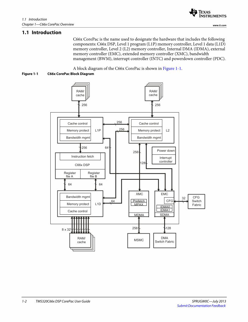
1.1 Introduction
1-2 TMS320C66x DSP CorePac User Guide SPRUGW0C—July 2013Submit Documentation Feedback
Chapter 1—C66x CorePac Overview www.ti.com
1.1 IntroductionC66x CorePac is the name used to designate the hardware that includes the following components: C66x DSP, Level 1 program (L1P) memory controller, Level 1 data (L1D) memory controller, Level 2 (L2) memory controller, Internal DMA (IDMA), external memory controller (EMC), extended memory controller (XMC), bandwidth management (BWM), interrupt controller (INTC) and powerdown controller (PDC).
A block diagram of the C66x CorePac is shown in Figure 1-1.Figure 1-1 C66x CorePac Block Diagram
Cache control
Memory protect
Bandwidth mgmt
L1P
RAM/cache
256
Bandwidth mgmt
Memory protect
Cache control
256
L2
RAM/cache
256
Instruction fetch
file A file B
C66x DSP
256
Cache control
Memory protect
Bandwidth mgmt
L1D
64 64
8 x 32
256
64
64
Power down
Interruptcontroller
CFG
MDMA SDMA
EMC
256
32 CFGSwitch Fabric
256 128
RAM/cache
Register Register
DMASwitch Fabric
XMC
PrefetchMPAX
MSMC
IDMA0IDMA1
128

1.2 C66x CorePac Overview
SPRUGW0C—July 2013 TMS320C66x DSP CorePac User Guide 1-3Submit Documentation Feedback
Chapter 1—C66x CorePac Overviewwww.ti.com
1.2 C66x CorePac OverviewThe following sections provide an overview of the main components and features of the C66x CorePac.
1.2.1 C66x DSPThe C66x DSP is the next-generation fixed-point and floating-point DSP. The new DSP enhances the C674x, which merged the C67x+ floating point and the C64x+ fixed-point instruction set architectures.
The C66x DSP is object-code compatible with the C64x+/C674x DSP.
The C66x DSP is not described further in this document. For more information on the C66x DSP, see the C66x DSP and Instruction Set Reference Guide (SPRUGH7) in ‘‘Related Documentation from Texas Instruments’’ on page ø-xx.
1.2.2 Level 1 Program (L1P) Memory ControllerThe L1P memory controller interfaces the DSP fetch pipeline to L1P memory. You can configure part of the L1P memory as a one-way set-associative cache. Cache sizes of 4KB, 8KB, 16KB, or 32KB are supported.
The L1P provides bandwidth management, memory protection, and power-down support. The L1P memory is always initiated to either all SRAM or maximum cache after reset. The behavior is specific to each C66x device.
For more information on the L1P cache/memory, see Chapter 2 on page 2-1.
1.2.3 Level 1 Data (L1D) Memory ControllerThe L1D memory controller interfaces the DSP data path to L1D memory. Part of the L1D memory can be configured as a two way set-associative cache. Cache sizes of 4KB, 8KB, 16KB, or 32KB are supported.
The L1D provides bandwidth management, memory protection, and power-down support. The L1D memory is always initiated to either all SRAM or maximum cache after reset. The behavior is specific to each device.
For more information on the L1D cache/memory, see Chapter 3 on page 3-1.
1.2.4 Level 2 (L2) Memory ControllerThe L2 memory controller interfaces level 1 memories to higher-level memories. Part of the L2 memory can be configured as a four way set-associative cache. Cache sizes of 32KB, 64KB, 128KB, 256KB, 512KB or 1MB are supported.
The L2 provides bandwidth management, memory protection, and power-down support. The L2 memory is always initiated to all SRAM after reset. If you want to initiate cache modes, you must do so during device run time.
If you configure part of internal memory as cache, the L2 controller provides a means of writing back changes made to its contents, or invalidating the cache's contents altogether. This can be performed on a block or global basis. These actions constitute coherence operations that you specify; that is, they are intended to make the cached information coherent with the original memory location's content. Writebacks and invalidations also occur automatically by virtue of how cache architectures operate.
1.2 C66x CorePac Overview
1-4 TMS320C66x DSP CorePac User Guide SPRUGW0C—July 2013Submit Documentation Feedback
Chapter 1—C66x CorePac Overview www.ti.com
These activities are generally called coherence operations throughout this document. Coherence operations are described in more detail in Chapter 2 on page 2-1, Chapter 3 on page 3-1, and Chapter 4 on page 4-1.
See Chapter 4 on page 4-1 for more information on the L2 cache/memory.
1.2.5 Internal DMA (IDMA)The internal DMA (IDMA) is a DMA local to the CorePac—that is, it provides data move services only within the CorePac (L1P, L1D, L2, and CFG).
There are two IDMA channels (0 and 1):• Channel 0 allows data to transfer between the peripheral configuration space
(CFG) and any local memories (L1P, L1D, and L2). • Channel 1 enables data to transfer between the local memories (L1P, L1D, and
L2).
The IDMA data transfers occur in the background of DSP operation. That is, once a channel transfer is programmed, it happens concurrent with other DSP activity, and without additional DSP intervention.
For more information on the IDMA, see Chapter 5 on page 5-1.
1.2.6 External Memory Controller (EMC)The external memory controller (EMC) is a bridge from the CorePac to the rest of the device. It includes two ports:
• Configuration registers (CFG)—This port provides access to the memory-mapped registers which control various peripherals and resources on C66x devices.
Note—This port does not provide access to those control registers found within the DSP or the CorePac.
• Slave DMA (SDMA)—The slave DMA provides access to resources inside the C66x CorePac to system masters found outside the C66x CorePac such as DMA controllers, SRIO, etc. That is, transfers initiated outside the C66x CorePac where the C66x CorePac is the slave in the transaction.
The CFG bus is always 32 bits wide, and should always be accessed as 32-bit values using 32-bit load /store instructions or the IDMA. The SDMA port is 128 bits wide.
See Chapter 6 on page 6-1 for more information on the EMC.
1.2.7 Extended Memory Controller (XMC)The XMC is responsible for the L2 memory controller’s path to the Multicore Shared Memory Controller (MSMC). The XMC performs various roles as listed below:
• Shared memory access path• Memory protection for addresses outside C66x CorePac—e.g. MSMC RAM or
EMIF • Address extension/translation (32-bit to 36-bit)• Prefetch support
1.2 C66x CorePac Overview
SPRUGW0C—July 2013 TMS320C66x DSP CorePac User Guide 1-5Submit Documentation Feedback
Chapter 1—C66x CorePac Overviewwww.ti.com
Memory protection and address extension are provided together in a new unit called MPAX. The MPAX unit defines 16 segments of runtime-selectable size that project C66x CorePac’s 32-bit logical address space into a larger 36-bit physical address space. In addition, each segment has a corresponding set of permissions to control accesses to that segment. The two together provide a convenient mechanism for multiple DSPs to cooperate in a large shared memory. The memory protection scheme is also designed to coordinate with other memory protection units and firewalls that may be in the system.
Prefetch support in XMC aims to reduce the read miss penalty for streams of data entering C66x CorePac. Hence prefetching helps to reduce stall cycles and thereby improves memory read performance to MSMC RAM and EMIF.
See Chapter 7 on page 7-1 for more information on the XMC.
1.2.8 Bandwidth Management (BWM)The C66x CorePac includes a set of resources (L1P, L1D, L2, and configuration bus) and a set of requestors (DSP, SDMA, IDMA, and coherence operations) that need to use these resources. In order to avoid blocking a requestor from accessing a resource for a long period of time, the C66x CorePac implements a bandwidth management scheme in order to assure some bandwidth to all of the requestors.
See Chapter 8 on page 8-1 for more information on the BWM.
1.2.9 Interrupt Controller (INTC)The C66x DSP provides two types of asynchronous signaling services:
• Interrupts • Exceptions
Interrupts provide the means to redirect normal program flow due to the presence of an external or internal hardware signal. Exceptions are similar in that they also redirect program flow, but they are normally associated with error conditions in the system.
The C66x DSP can receive 12 maskable/configurable interrupts, 1 maskable exception, and 1 unmaskable interrupt/exception. The DSP can also respond to a variety of internal exception conditions, though these are documented in the C66x CPU and Instruction Set Reference Guide (SPRUGH7), since they are wholly contained within the DSP.
The C66x CorePac includes an interrupt controller that allows up to 128 system events to be routed to the DSP interrupt/exception inputs. These 128 events can either be directly connected to the maskable interrupts, or grouped together as interrupts or exceptions. These various routing choices allow a great deal of flexibility in event handling.
An error event is signaled when an interrupt is signaled to the DSP and there is already a flag pending for this interrupt. In addition to routing events, the interrupt controller detects when the DSP misses an interrupt. You can use this error event to notify the DSP when it misses a real time event. The INTC hardware saves the missed interrupt number in a register so that corrective action can be taken.
See Chapter 9 on page 9-1 for more information on the INTC.

1.2 C66x CorePac Overview
1-6 TMS320C66x DSP CorePac User Guide SPRUGW0C—July 2013Submit Documentation Feedback
Chapter 1—C66x CorePac Overview www.ti.com
1.2.10 Memory Protection Architecture (MPA)The C66x CorePac offers memory protection support for its local memories (L1P, L1D, and L2). System level memory protection is device-specific and is not available on all devices. See the device-specific data sheet for more information.
Memory protection is defined globally, but implemented locally. Thus, the overall protection scheme is defined for the entire C66x CorePac, but each resource implements its own protection hardware. This distributed method of memory protection means you only need to learn one memory protection interface, while the C66x remains flexible enough to support future peripherals and memories.
To implement the memory protection scheme, the memory map is divided into “pages” and each page has an associated set of permissions. Invalid accesses are signaled with an exception and reported to the system in memory fault registers. Additionally, MPA supports privilege modes (supervisor and user) and memory locks.
Due to the distributed implementation of the memory protection scheme, the overall definitions are described in Chapter 10 on page 10-1. See each resource's chapter for specific details for MPA implementation.
1.2.11 Power-Down Controller (PDC)The power-down controller allows software-driven power-down management for all of the C66x CorePac components. The DSP can power-down all or part of the C66x CorePac through the power-down controller based on its own execution thread or in response to an external stimulus from a host or global controller.
See Chapter 12 on page 12-1 for more information on the PDC.

SPRUGW0C—July 2013 TMS320C66x DSP CorePac User Guide 2-1Submit Documentation Feedback
Chapter 2
Level 1 Program Memory and Cache
2.1 "Introduction" on page 2-2 2.2 "L1 Program Memory Architecture" on page 2-2 2.3 "L1P Cache" on page 2-3 2.4 "Program Initiated Coherence Operations" on page 2-7 2.5 "L1P Cache Control Registers" on page 2-9 2.6 "L1P Performance" on page 2-13 2.7 "L1P Power-Down Support" on page 2-15 2.8 "L1P Memory Protection" on page 2-16
2.1 Introduction
2-2 TMS320C66x DSP CorePac User Guide SPRUGW0C—July 2013Submit Documentation Feedback
Chapter 2—Level 1 Program Memory and Cache www.ti.com
2.1 Introduction2.1.1 Purpose of the Level 1 Program (L1P) Memory and Cache
The purpose of the Level 1 program (L1P) memory and cache is to maximize performance of the code execution. The configurability of the L1P cache offers the flexibility required in many systems.
2.1.2 FeaturesThe L1P memory and cache provide the memory flexibility that is required in devices that use the C66x CorePac.
• Configurable L1P cache size: 0K, 4K, 8K, 16K, and 32K• Memory protection• Cache block and global coherence operations
2.1.3 Terms and DefinitionsSee Appendix A and Appendix B of this document for detailed definitions of the terms used in this chapter. Appendix A on page A-1 describes general terms used throughout this document and Appendix B on page B-1 defines terms related to the memory and cache architecture.
2.2 L1 Program Memory Architecture2.2.1 L1P Memory
L1P memory supports up to 128 Kbytes of RAM. L1P memory cannot be cached within Level 1 data (L1D) cache, Level 1program (L1P) cache, or Level 2 (L2) cache within the same C66x CorePac.
The L1P memory's base address is constrained to 1 MB boundaries. The total size of L1P memory must be a multiple of 16 Kbytes.
The actual memory configuration is device-specific. See the device-specific data sheet for more information.
2.2.1.1 L1P AccessThe L1P memory can only be written to using EDMA or IDMA accesses; the L1P memory cannot be written to using DSP stores. The L1P memory can be read from using EDMA, IDMA, or DSP accesses.
2.2.1.2 L1P Wait StatesThe maximum number of wait states is 3. The number of wait states is not configurable in software, it is defined when the chip is created. L1P SRAM typically has 0 wait states. See the device-specific data sheet for more information.
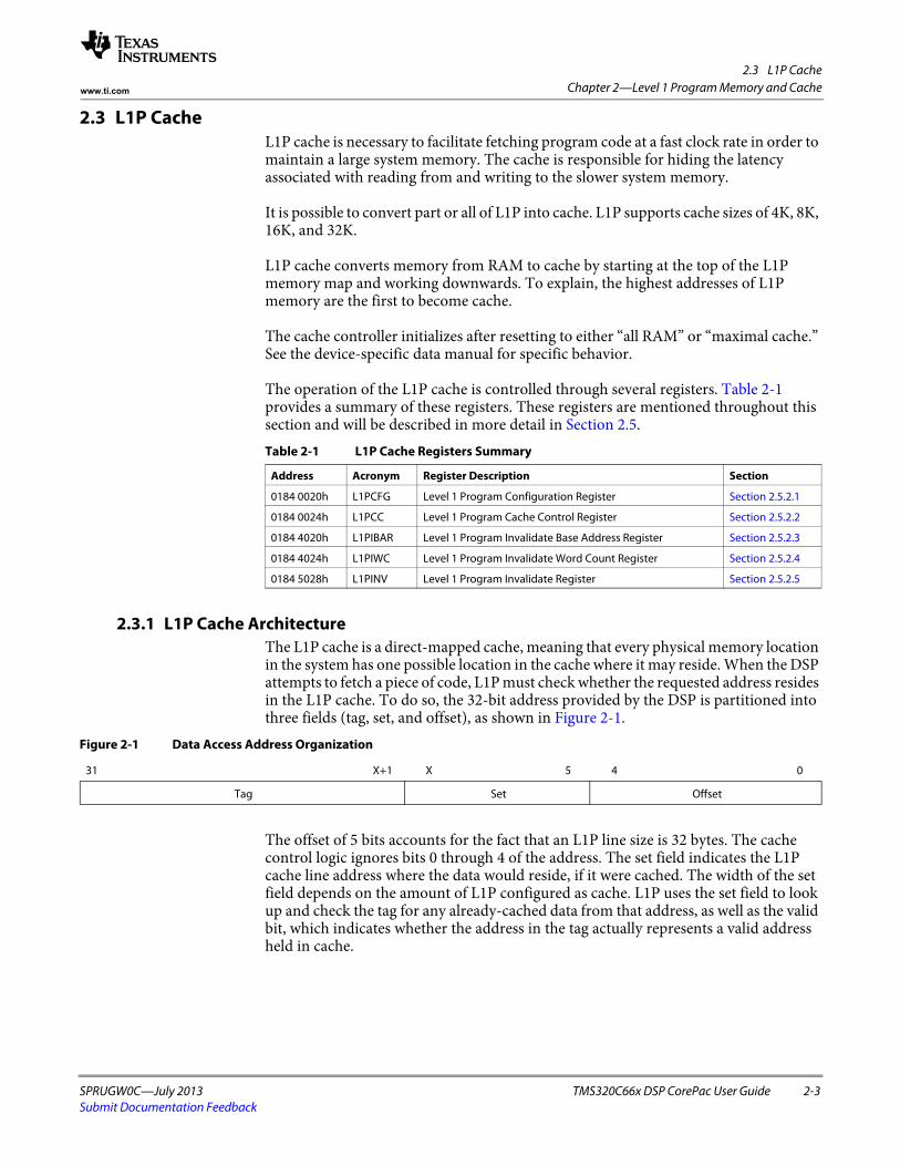
2.3 L1P Cache
SPRUGW0C—July 2013 TMS320C66x DSP CorePac User Guide 2-3Submit Documentation Feedback
Chapter 2—Level 1 Program Memory and Cachewww.ti.com
2.3 L1P CacheL1P cache is necessary to facilitate fetching program code at a fast clock rate in order to maintain a large system memory. The cache is responsible for hiding the latency associated with reading from and writing to the slower system memory.
It is possible to convert part or all of L1P into cache. L1P supports cache sizes of 4K, 8K, 16K, and 32K.
L1P cache converts memory from RAM to cache by starting at the top of the L1P memory map and working downwards. To explain, the highest addresses of L1P memory are the first to become cache.
The cache controller initializes after resetting to either “all RAM” or “maximal cache.” See the device-specific data manual for specific behavior.
The operation of the L1P cache is controlled through several registers. Table 2-1 provides a summary of these registers. These registers are mentioned throughout this section and will be described in more detail in Section 2.5.
2.3.1 L1P Cache ArchitectureThe L1P cache is a direct-mapped cache, meaning that every physical memory location in the system has one possible location in the cache where it may reside. When the DSP attempts to fetch a piece of code, L1P must check whether the requested address resides in the L1P cache. To do so, the 32-bit address provided by the DSP is partitioned into three fields (tag, set, and offset), as shown in Figure 2-1.
The offset of 5 bits accounts for the fact that an L1P line size is 32 bytes. The cache control logic ignores bits 0 through 4 of the address. The set field indicates the L1P cache line address where the data would reside, if it were cached. The width of the set field depends on the amount of L1P configured as cache. L1P uses the set field to look up and check the tag for any already-cached data from that address, as well as the valid bit, which indicates whether the address in the tag actually represents a valid address held in cache.
Table 2-1 L1P Cache Registers Summary
Address Acronym Register Description Section
0184 0020h L1PCFG Level 1 Program Configuration Register Section 2.5.2.1
0184 0024h L1PCC Level 1 Program Cache Control Register Section 2.5.2.2
0184 4020h L1PIBAR Level 1 Program Invalidate Base Address Register Section 2.5.2.3
0184 4024h L1PIWC Level 1 Program Invalidate Word Count Register Section 2.5.2.4
0184 5028h L1PINV Level 1 Program Invalidate Register Section 2.5.2.5
Figure 2-1 Data Access Address Organization
31 X+1 X 5 4 0
Tag Set Offset
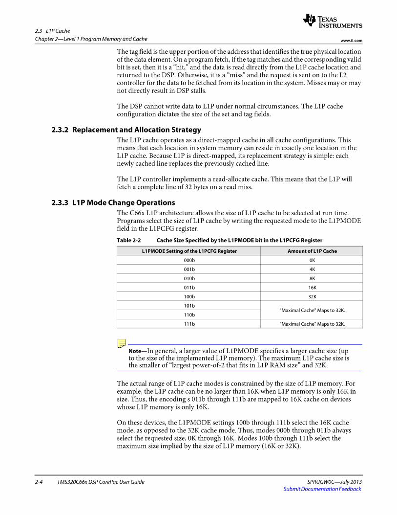
2.3 L1P Cache
2-4 TMS320C66x DSP CorePac User Guide SPRUGW0C—July 2013Submit Documentation Feedback
Chapter 2—Level 1 Program Memory and Cache www.ti.com
The tag field is the upper portion of the address that identifies the true physical location of the data element. On a program fetch, if the tag matches and the corresponding valid bit is set, then it is a “hit,” and the data is read directly from the L1P cache location and returned to the DSP. Otherwise, it is a “miss” and the request is sent on to the L2 controller for the data to be fetched from its location in the system. Misses may or may not directly result in DSP stalls.
The DSP cannot write data to L1P under normal circumstances. The L1P cache configuration dictates the size of the set and tag fields.
2.3.2 Replacement and Allocation Strategy The L1P cache operates as a direct-mapped cache in all cache configurations. This means that each location in system memory can reside in exactly one location in the L1P cache. Because L1P is direct-mapped, its replacement strategy is simple: each newly cached line replaces the previously cached line.
The L1P controller implements a read-allocate cache. This means that the L1P will fetch a complete line of 32 bytes on a read miss.
2.3.3 L1P Mode Change OperationsThe C66x L1P architecture allows the size of L1P cache to be selected at run time. Programs select the size of L1P cache by writing the requested mode to the L1PMODE field in the L1PCFG register.
Note—In general, a larger value of L1PMODE specifies a larger cache size (up to the size of the implemented L1P memory). The maximum L1P cache size is the smaller of “largest power-of-2 that fits in L1P RAM size” and 32K.
The actual range of L1P cache modes is constrained by the size of L1P memory. For example, the L1P cache can be no larger than 16K when L1P memory is only 16K in size. Thus, the encoding s 011b through 111b are mapped to 16K cache on devices whose L1P memory is only 16K.
On these devices, the L1PMODE settings 100b through 111b select the 16K cache mode, as opposed to the 32K cache mode. Thus, modes 000b through 011b always select the requested size, 0K through 16K. Modes 100b through 111b select the maximum size implied by the size of L1P memory (16K or 32K).
Table 2-2 Cache Size Specified by the L1PMODE bit in the L1PCFG Register
L1PMODE Setting of the L1PCFG Register Amount of L1P Cache
000b 0K
001b 4K
010b 8K
011b 16K
100b 32K
101b"Maximal Cache" Maps to 32K.
110b
111b "Maximal Cache" Maps to 32K.
2.3 L1P Cache
SPRUGW0C—July 2013 TMS320C66x DSP CorePac User Guide 2-5Submit Documentation Feedback
Chapter 2—Level 1 Program Memory and Cachewww.ti.com
As a result of this policy, programs wanting no more than a certain amount of cache should program the value corresponding to this upper bound. Programs that want “as much cache as possible” should program 111b into L1PMODE.
When programs initiate a cache mode change, the L1P cache itself invalidates its current contents. This ensures that no false hits occur due to changing interpretation of cache tags.
While the invalidation is necessary to ensure correct cache behavior, it is not sufficient to prevent data loss due to portions of L1P RAM becoming cache. Thus, to safely change L1P cache modes, applications must adhere to the procedure in Table 2-3.
2.3.4 L1P Freeze Mode The L1P cache directly supports a freeze mode of operation for applications. This mode allows applications to prevent DSP data accesses from evicting program code from the cache. This feature is useful in an interrupt context. L1P freeze mode only affects L1P cache. L1P RAM is not affected by freeze mode.
While in freeze mode, the L1P cache will service read hits normally. Read hits return data from the cache. In freeze mode, the L1P cache will not allocate new cache lines on read misses, nor will it cause any existing cache contents to be marked invalid.
The OPER field in the L1PCC register controls whether L1P is frozen or it is operating normally, as shown in Example 2-1.
The DSP places L1P into freeze mode by writing 001b to the OPER field in the L1PCC register. The DSP returns L1P to normal operation by writing 0b to the OPER field in the L1PCC register.
The POPER field in the L1PCC register holds the previous value of the OPER field. The value of the OPER field is copied to the POPER field in the L1PCC register on writes to the L1PCC register. Copying the value of the OPER field to the POPER field alleviates the cycle cost of reading the L1PCC register (in order to save the previous value of the OPER field) before it is written. If the POPER field is not in the L1PCC register, the program must read, write, and then read again to fully freeze the cache while recording its previous operating mode. If the POPER field is in the L1PCC register, this operation reduces to a single write followed by a read.
When you write to the L1PCC register, the following operations occur:1. The OPER field copies to the POPER field in the L1PCC register.2. The POPER field loses its previous value.
Table 2-3 Switching L1P Modes
To switch from. . . To. . . The program must perform the following steps. . .
A mode with no or some L1P cache A mode with more L1P cache 1. DMA, IDMA or copy any needed data out of the affected range of L1P RAM.(If none requires saving, no DMA is necessary).
2. Write the desired cache mode to the L1PMODE field in the L1PCFG register.
3. Read back L1PCFG. This stalls the DSP until the mode change completes.
A mode with some L1P cache A mode with less or no L1P cache 1. Write the desired cache mode to the L1PMODE field in the L1PCFG register.
2. Read back L1PCFG. This stalls the DSP until the mode change completes.
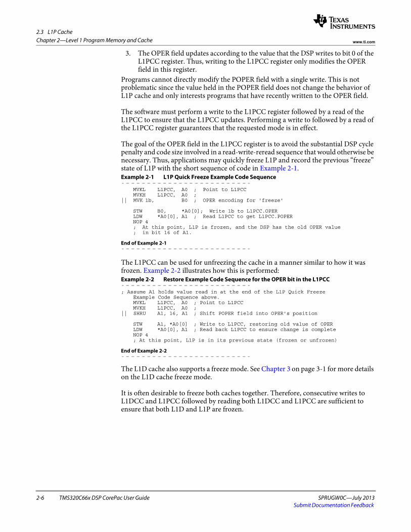
2.3 L1P Cache
2-6 TMS320C66x DSP CorePac User Guide SPRUGW0C—July 2013Submit Documentation Feedback
Chapter 2—Level 1 Program Memory and Cache www.ti.com
3. The OPER field updates according to the value that the DSP writes to bit 0 of the L1PCC register. Thus, writing to the L1PCC register only modifies the OPER field in this register.
Programs cannot directly modify the POPER field with a single write. This is not problematic since the value held in the POPER field does not change the behavior of L1P cache and only interests programs that have recently written to the OPER field.
The software must perform a write to the L1PCC register followed by a read of the L1PCC to ensure that the L1PCC updates. Performing a write to followed by a read of the L1PCC register guarantees that the requested mode is in effect.
The goal of the OPER field in the L1PCC register is to avoid the substantial DSP cycle penalty and code size involved in a read-write-reread sequence that would otherwise be necessary. Thus, applications may quickly freeze L1P and record the previous “freeze” state of L1P with the short sequence of code in Example 2-1. Example 2-1 L1P Quick Freeze Example Code Sequence
MVKL L1PCC, A0 ; Point to L1PCCMVKH L1PCC, A0 ;
|| MVK 1b, B0 ; OPER encoding for 'freeze'
STW B0, *A0[0]; Write 1b to L1PCC.OPERLDW *A0[0], A1 ; Read L1PCC to get L1PCC.POPERNOP 4; At this point, L1P is frozen, and the DSP has the old OPER value ; in bit 16 of A1.
End of Example 2-1
The L1PCC can be used for unfreezing the cache in a manner similar to how it was frozen. Example 2-2 illustrates how this is performed: Example 2-2 Restore Example Code Sequence for the OPER bit in the L1PCC
; Assume A1 holds value read in at the end of the L1P Quick Freeze Example Code Sequence above. MVKL L1PCC, A0 ; Point to L1PCCMVKH L1PCC, A0 ;
|| SHRU A1, 16, A1 ; Shift POPER field into OPER's position
STW A1, *A0[0] ; Write to L1PCC, restoring old value of OPERLDW *A0[0], A1 ; Read back L1PCC to ensure change is completeNOP 4; At this point, L1P is in its previous state (frozen or unfrozen)
End of Example 2-2
The L1D cache also supports a freeze mode. See Chapter 3 on page 3-1 for more details on the L1D cache freeze mode.
It is often desirable to freeze both caches together. Therefore, consecutive writes to L1DCC and L1PCC followed by reading both L1DCC and L1PCC are sufficient to ensure that both L1D and L1P are frozen.

2.4 Program Initiated Coherence Operations
SPRUGW0C—July 2013 TMS320C66x DSP CorePac User Guide 2-7Submit Documentation Feedback
Chapter 2—Level 1 Program Memory and Cachewww.ti.com
Example 2-3 illustrates a sequence that freezes both L1D and L1P. Example 2-3 Example Code Sequence for Freezing L1D and L1P Simultaneously
MVKL L1DCC, A0 ; \|| MVKL L1PCC, B0 ; |__ Generate L1DCC pointer in A0
MVKH L1DCC, A0 ; | and L1PCC pointer in B0|| MVKH L1PCC, B0 ; /|| MVK 1b, A1 ; \___ OPER encoding for 'freeze'|| MVK 1b, B1 ; / in both A1 and B1.
STW A1, *A0 ; Write to L1DCC.OPER|| STW B1, *B0 ; Write to L1PCC.OPER
LDW *A0,A1 ; Get old freeze state into A1 from L1DCC|| LDW *B0,B1 ; Get old freeze state into B1 from L1PCC
NOP 4; At this point, L1D and L1P are frozen. ; The old value of L1DCC.OPER is in bit 16 of A1.; The old value of L1PCC.OPER is in bit 16 of B1.
End of Example 2-3
2.4 Program Initiated Coherence OperationsThe C66x L1P architecture supports program-initiated cache coherence operations. These operations operate either on a block of addresses or on the entire L1P cache.
2.4.1 Global Coherence Operation Global cache operations synchronize L1P with “the system” between major events, such as a task switch, L1P mode change, or change to memory protection settings. Thus, global cache operations are viewed as “synchronous” with respect to other program activity.
You can globally invalidate the L1P cache under software control. The program must write a 1 to the I bit of the L1PINV register in order to initiate a global invalidation operation.
During the global invalidation of the L1P cache, no writeback operation is performed because code is not modified.
The I bit of the L1PINV register resets to 0 upon completion of the global coherence operation. The program can poll this field to detect the completion of the operation. The polling code must be located outside the L1P cache.
Table 2-4 provides a summary of the L1P global coherence operations.
You can also globally invalidate the L1P cache by setting the IP bit in the L2CFG register to 1. The IP bit provides backward compatibility with C66x devices. You should not use the IP bit in new applications; use the L1PINV register for new applications.
2.4.2 Block Coherence Operation Block coherence operations have similar functionality as the global coherence operation; however, they apply only to a defined block of code. This block is defined by the base address and the word size (32-bit) in the associated L1PIBAR and L1PIWC, respectively.
Table 2-4 L1P Global Coherence Operations
Cache Operation Register Used L1P Effect
L1P Invalidate L1PINV All lines invalidated in L1P.
2.4 Program Initiated Coherence Operations
2-8 TMS320C66x DSP CorePac User Guide SPRUGW0C—July 2013Submit Documentation Feedback
Chapter 2—Level 1 Program Memory and Cache www.ti.com
The L1P invalidate word count field of the L1PIWC sets to 0 upon completion of the block coherence operation. The program can poll this field to detect the completion of the operation. The polling code must be located outside of the affected block of the L1P cache.
On the C66x DSP, it is recommended that programs wait for block coherence operations to complete before continuing. To issue a block coherence operation:
1. Write the starting address to the L1PIBAR register.2. Write the word count to the L1PIWC register.3. Wait for completion by one of the following methods:
a. Issue an MFENCE instruction (preferred), orb. Poll the L1PIWC register until the word count field reads as zero.
The MFENCE instruction is new to the C66x DSP. It stalls the DSP until all outstanding memory operations complete. For further information about MFENCE instruction, see the C66x DSP and Instruction Set Reference Guide (SPRUGH7) in ‘‘Related Documentation from Texas Instruments’’ on page ø-xx.
Table 2-5 provides a summary of the L1P block cache operations. Table 2-5 L1P Block Cache Operations
Cache Operation Register Used L1P Effect
L1P Invalidate L1PIBAR
L1PIWC
All lines in range invalidated in L1P.
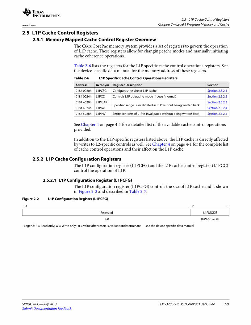
2.5 L1P Cache Control Registers
SPRUGW0C—July 2013 TMS320C66x DSP CorePac User Guide 2-9Submit Documentation Feedback
Chapter 2—Level 1 Program Memory and Cachewww.ti.com
2.5 L1P Cache Control Registers2.5.1 Memory Mapped Cache Control Register Overview
The C66x CorePac memory system provides a set of registers to govern the operation of L1P cache. These registers allow for changing cache modes and manually initiating cache coherence operations.
Table 2-6 lists the registers for the L1P specific cache control operations registers. See the device-specific data manual for the memory address of these registers.
See Chapter 4 on page 4-1 for a detailed list of the available cache control operations provided.
In addition to the L1P-specific registers listed above, the L1P cache is directly affected by writes to L2-specific controls as well. See Chapter 4 on page 4-1 for the complete list of cache control operations and their affect on the L1P cache.
2.5.2 L1P Cache Configuration RegistersThe L1P configuration register (L1PCFG) and the L1P cache control register (L1PCC) control the operation of L1P.
2.5.2.1 L1P Configuration Register (L1PCFG)The L1P configuration register (L1PCFG) controls the size of L1P cache and is shown in Figure 2-2 and described in Table 2-7.
Table 2-6 L1P Specific Cache Control Operations Registers
Address Acronym Register Description Section
0184 0020h L1PCFG Configures the size of L1P cache Section 2.5.2.1
0184 0024h L1PCC Controls L1P operating mode (freeze / normal) Section 2.5.2.2
0184 4020h L1PIBARSpecified range is invalidated in L1P without being written back
Section 2.5.2.3
0184 4024h L1PIWC Section 2.5.2.4
0184 5028h L1PINV Entire contents of L1P is invalidated without being written back Section 2.5.2.5
Figure 2-2 L1P Configuration Register (L1PCFG)
31 3 2 0
Reserved L1PMODE
R-0 R/W-0h or 7h
Legend: R = Read only; W = Write only; -n = value after reset; -x, value is indeterminate — see the device-specific data manual
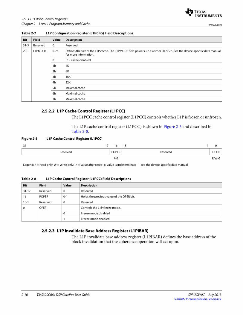
2.5 L1P Cache Control Registers
2-10 TMS320C66x DSP CorePac User Guide SPRUGW0C—July 2013Submit Documentation Feedback
Chapter 2—Level 1 Program Memory and Cache www.ti.com
2.5.2.2 L1P Cache Control Register (L1PCC)The L1PCC cache control register (L1PCC) controls whether L1P is frozen or unfrozen.
The L1P cache control register (L1PCC) is shown in Figure 2-3 and described in Table 2-8.
2.5.2.3 L1P Invalidate Base Address Register (L1PIBAR) The L1P invalidate base address register (L1PIBAR) defines the base address of the block invalidation that the coherence operation will act upon.
Table 2-7 L1P Configuration Register (L1PCFG) Field Descriptions
Bit Field Value Description
31-3 Reserved 0 Reserved
2-0 L1PMODE 0-7h Defines the size of the L1P cache. The L1PMODE field powers-up as either 0h or 7h. See the device-specific data manual for more information.
0 L1P cache disabled
1h 4K
2h 8K
3h 16K
4h 32K
5h Maximal cache
6h Maximal cache
7h Maximal cache
Figure 2-3 L1P Cache Control Register (L1PCC)
31 17 16 15 1 0
Reserved POPER Reserved OPER
R-0 R/W-0
Legend: R = Read only; W = Write only; -n = value after reset; -x, value is indeterminate — see the device-specific data manual
Table 2-8 L1P Cache Control Register (L1PCC) Field Descriptions
Bit Field Value Description
31-17 Reserved 0 Reserved
16 POPER 0-1 Holds the previous value of the OPER bit.
15-1 Reserved 0 Reserved
0 OPER Controls the L1P freeze mode.
0 Freeze mode disabled
1 Freeze mode enabled

2.5 L1P Cache Control Registers
SPRUGW0C—July 2013 TMS320C66x DSP CorePac User Guide 2-11Submit Documentation Feedback
Chapter 2—Level 1 Program Memory and Cachewww.ti.com
The L1P invalidate base address register (L1PIBAR) is shown in Figure 2-4 and described in Table 2-9.
2.5.2.4 L1P Invalidate Word Count (L1PIWC)
The L1P invalidate word count register (L1PIWC) defines the size of the block invalidation that the coherence operation will act upon. The size is defined in 32-bit words.
The L1P invalidate word count register (L1PIWC) is shown in Figure 2-5 and described in Table 2-10.
2.5.2.5 L1P Invalidate Register (L1PINV)The L1P invalidate register (L1PINV) controls the global invalidation of the L1P cache and is shown in Figure 2-6 and described in Table 2-11.
Figure 2-4 L1P Invalidate Base Address Register (L1PIBAR)
31 0
L1P Invalidate Base Address
W-x
Legend: R = Read only; W = Write only; -n = value after reset; -x, value is indeterminate — see the device-specific data manual
Table 2-9 L1P Invalidate Base Address Register (L1PIBAR) Field Descriptions
Bit Field Value Description
31-0 L1PIBAR 0-FFFF FFFFh 32-bit base address for block invalidation.
Figure 2-5 L1P Invalidate Word Count Register (L1PIWC)
31 16 15 0
Reserved L1P Invalidate Word Count
R-0 R/W-0
Legend: R = Read only; W = Write only; -n = value after reset; -x, value is indeterminate — see the device-specific data manual
Table 2-10 L1P Invalidate Word Count Register (L1PIWC) Field Descriptions
Bit Field Value Description
31-16 Reserved 0 Reserved
15-0 L1PIWC 0-FFFFh Word count for block invalidation.
Figure 2-6 L1P Invalidate Register (L1PINV)
31 1 0
Reserved I
R-0 R/W-0
Legend: R = Read only; W = Write only; -n = value after reset; -x, value is indeterminate — see the device-specific data manual
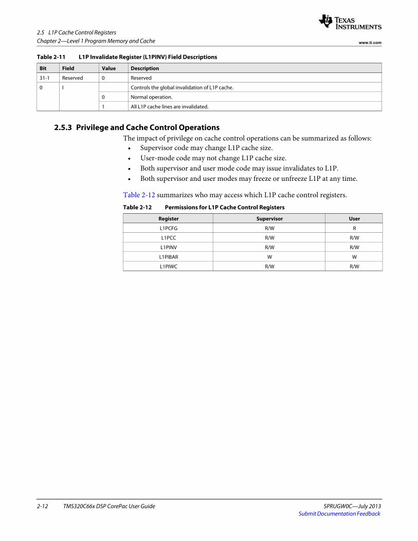
2.5 L1P Cache Control Registers
2-12 TMS320C66x DSP CorePac User Guide SPRUGW0C—July 2013Submit Documentation Feedback
Chapter 2—Level 1 Program Memory and Cache www.ti.com
2.5.3 Privilege and Cache Control OperationsThe impact of privilege on cache control operations can be summarized as follows:
• Supervisor code may change L1P cache size. • User-mode code may not change L1P cache size.• Both supervisor and user mode code may issue invalidates to L1P.• Both supervisor and user modes may freeze or unfreeze L1P at any time.
Table 2-12 summarizes who may access which L1P cache control registers.
Table 2-11 L1P Invalidate Register (L1PINV) Field Descriptions
Bit Field Value Description
31-1 Reserved 0 Reserved
0 I Controls the global invalidation of L1P cache.
0 Normal operation.
1 All L1P cache lines are invalidated.
Table 2-12 Permissions for L1P Cache Control Registers
Register Supervisor User
L1PCFG R/W R
L1PCC R/W R/W
L1PINV R/W R/W
L1PIBAR W W
L1PIWC R/W R/W
2.6 L1P Performance
SPRUGW0C—July 2013 TMS320C66x DSP CorePac User Guide 2-13Submit Documentation Feedback
Chapter 2—Level 1 Program Memory and Cachewww.ti.com
2.6 L1P Performance2.6.1 L1P Miss Penalty
A program fetch which hits L1P completes in a single cycle without stalling the DSP. An L1P miss that hits in L2 may stall the DSP for up to X cycles, depending on the parallelism of the execute packets in the vicinity of the miss. Section 2.6.2 describes this in more detail.
An L1P miss that misses in L2 cache stalls the DSP until the L2 retrieves the data from external memory and transfers the data to the L1P, which then returns the data to the DSP. This delay depends upon the type of external memory used to hold the program, as well as other aspects of system loading.
The C66x DSP allows an execute packet to span two fetch packets. This spanning does not change the penalty for a single miss. However, if both fetch packets are not present in L1P, two cache misses occur.
2.6.2 L1P Miss Pipelining Miss pipelining can hide much of this overhead by overlapping the processing for several cache misses. Additionally, some amount of the cache miss overhead can be overlapped with dispatch stalls that occur in the fetch pipeline.
For L1P miss pipelining to be effective, there must be multiple outstanding cache misses. The C66x DSP fetch pipeline accomplishes this by attempting to fetch one new fetch packet every cycle, as long as there is room in the fetch pipeline. To understand how this works, it is necessary to understand the nature of the fetch pipeline itself.
The fetch and decode pipeline is divided into 6 stages leading up to, but not including the first execution stage, E1. The stages are:
• PG: Program Generate • PS: Program Send • PW: Program Wait • PR: Program Read • DP: Dispatch • DC: Decode
The C6000 DSP instructions are grouped into two groupings: fetch packets and execute packets. The DSP fetches instructions from memory in fixed bundles of 8 instructions, known as fetch packets. The instructions are decoded and separated into bundles of parallel-issue instructions known as execute packets. A single execute packet may contain between 1 and 8 instructions. Thus, a single fetch packet may contain multiple execute packets. An execute packet may also span two fetch packets on the C66x DSP. The program read (PR) stage of the pipeline is responsible for identifying a sequence of execute packets within a sequence of fetch packets. The dispatch (DP) stage is responsible for extracting and dispatching them to functional units.

2.6 L1P Performance
2-14 TMS320C66x DSP CorePac User Guide SPRUGW0C—July 2013Submit Documentation Feedback
Chapter 2—Level 1 Program Memory and Cache www.ti.com
As a result of the disparity between fetch packets and execute packets, the entire fetch pipeline need not advance every cycle. Rather, the PR pipeline stage only allows the program wait (PW) stage to advance its contents into the PR stage when the DP stage has consumed the complete fetch packet held in PR. The stages before PR advance as needed to fill in gaps. Thus, when there are no cache misses, the early stages of the fetch pipeline are stalled while the DP stage pulls the individual execute packets from the current fetch packet. These stalls are referred to as dispatch stalls.
The C66x DSP takes advantage of these dispatch stalls by allowing the earlier stages of the pipeline to advance toward DP while cache misses for those stages are still pending. Cache misses may be pending for the PR, PW, and PS pipeline stages. It is not necessary to expose these cache stalls to the DSP because the DP stage stalls the PR stage with a dispatch stall while it consumes the fetch packets in the PR stage of the pipeline. When a fetch packet is consumed completely; however, the contents of the PW stage must advance into the PR stage. At this point, the DSP stalls if DP requests an execute packet from PR for which there is still an outstanding cache miss.
When a branch is taken, the fetch packet containing the branch target advances through the fetch pipeline every cycle until the branch target reaches the E1 pipeline stage. Branch targets override the dispatch stall described above. As a result, they do not gain as much benefit from miss pipelining as other instructions. However, the fetch packets that immediately follow a branch target do benefit. Although the code in the fetch packets that follows the branch target may not execute immediately, the branch triggers several consecutive fetches for this code. Thus, it pipelines any misses for that code. In addition, no stalls are registered for fetch packets that were requested prior to the branch being taken, but that never made it to the DP pipeline stage.
The miss performance is measured with sustained back-to-back misses in straight-line (non-branching) code incurs an average miss penalty based on the average parallelism of the code. The average miss penalty for a long sequence of sustained misses in straight-line code is summarized in Table 2-13. The code is fetched from L2SRAM. The configuration features 3 wait states for L2SRAM, 8 x 128 bit banks which is made up of two physical banks with four subbanks each. This configuration is available in the KeyStone devices.Table 2-13 L1P Miss Pipelining Performance (Average Number of Stalls per Execute Packet)
(TBD)
L2 Type 3 wait states, 8 x 128-bit banks
Instructions per Execute Packet L2 SRAM L2 Cache
1
2
3
4
5
6
7
8
2.7 L1P Power-Down Support
SPRUGW0C—July 2013 TMS320C66x DSP CorePac User Guide 2-15Submit Documentation Feedback
Chapter 2—Level 1 Program Memory and Cachewww.ti.com
2.7 L1P Power-Down SupportThe L1P memory can be powered-down in several ways in order to save power.
2.7.1 Static Power-DownThe L1P memory is powered down when the entire C66x CorePac is powered down.
The following software sequence is required to power down the C66x CorePac: 1. Enable power-down by setting the MEGPD field in the PDCCMD register to 1.2. Enable the DSP interrupt(s) that you want to wake the C66x CorePac up; disable
all others.3. Execute an IDLE instruction.
The C66x CorePac stays in powered-down mode until the interrupts enabled in step 2 above are awakened.
The power-down controller command register (PDCCMD) is described in Chapter 12 on page 12-1. If a DMA access occurs to the L1D, L1P, or L2 memory while the C66x CorePac is powered-down, the PDC wakes up all three memory controllers. When the DMA access has been serviced, the PDC will power-down the memory controllers again.
Note—Powering-down the C66x CorePac as described here is often called static power-down. This term is used to describe this mode since it is often used for longer periods of time. The use of the term dynamic power-down elsewhere in this chapter implies that they are used for limited periods of time.
2.7.2 Dynamic Power-DownThe L1P memory is automatically powered-down while the DSP executes code from the SPLOOP buffer. For more information about the SPLOOP buffer, see the C66x DSP CPU and Instruction Set Reference Guide (SPRUGH7) in ‘‘Related Documentation from Texas Instruments’’ on page ø-xx.
2.7.3 Feature-Oriented Power-DownWhen the L1P cache is disabled (000b is written to the MODE field of the L1PCFG register) it is in a power-down state to conserve energy further.

2.8 L1P Memory Protection
2-16 TMS320C66x DSP CorePac User Guide SPRUGW0C—July 2013Submit Documentation Feedback
Chapter 2—Level 1 Program Memory and Cache www.ti.com
2.8 L1P Memory ProtectionL1P memory supports memory protection to offer the robustness required in many systems. Several levels of memory protection are available. Not all of the levels are available on all of the devices. See the device-specific data manual for more information. See Chapter 10 on page 10-1 for the details of C66x protection.
2.8.1 Protection Checks on L1P Accesses Unlike the L1D, L1P implements different memory protection rules for DSP program fetches from L1P memory versus DSP DMA and IDMA accesses to L1P memory. The following sections detail those differences.
All three memory controllers feature two exception outputs which are routed to the C66x CorePac interrupt controller. One of these exception outputs indicates that a DSP-triggered (“local”) memory exception occurred. The other indicates that a DMA-triggered (“remote”) exception occurred. Most programs will likely route the DSP-triggered exception input to the DSP’s exception input and the DMA-triggered input to an interrupt input.
2.8.1.1 Protection Checks on DSP Program Fetches L1P performs memory protection checks on all fetches. Each fetch packet has two permission bits associated with it (shown in Table 2-14) that determine the execution privileges associated with the code contained within the cache line or corresponding region of L1P RAM. L1P provides the results of the permission checks for all fetches, regardless of where the fetched data eventually arrives from.
2.8.1.2 Protection Checks on DSP Data AccessesThe DSP cannot directly access L1P RAM via load and store instructions. However, it can attempt to access L1P’s control registers with load and store instructions.
The permissions associated with the registers are checked for reads of its registers. L1P checks writes off of its registers. It will signal a DSP-triggered memory exception in response to disallowed writes. The details of the exception are recorded in L1PMPFAR/L1PMPFSR, and L1P signals a DSP memory protection exception event (L1P_CMPA) to the interrupt controller.
2.8.1.3 Protection Checks on DMA/IDMA Accesses DMA and IDMA access to L1P memory are constrained to L1P RAM. DMA/IDMA cannot access L1P cache. Accesses to the L1P RAM under the L1P cache are governed by protection entries associated with the L1P RAM.
Each DMA/IDMA access is checked against the SR/SW/UR/UW and accessor ID fields for the corresponding memory protection page. DMA/IDMA accesses to L1P memory index into the 16 memory protection pages.
Table 2-14 Permission Bits Examined With Each Fetch
Bit Description
UX User mode may eXecute
SX Supervisor mode may eXecute
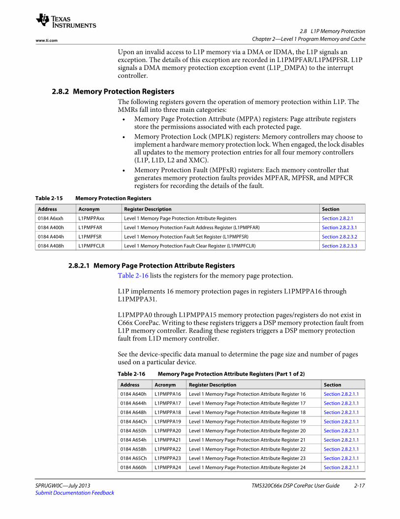
2.8 L1P Memory Protection
SPRUGW0C—July 2013 TMS320C66x DSP CorePac User Guide 2-17Submit Documentation Feedback
Chapter 2—Level 1 Program Memory and Cachewww.ti.com
Upon an invalid access to L1P memory via a DMA or IDMA, the L1P signals an exception. The details of this exception are recorded in L1PMPFAR/L1PMPFSR. L1P signals a DMA memory protection exception event (L1P_DMPA) to the interrupt controller.
2.8.2 Memory Protection RegistersThe following registers govern the operation of memory protection within L1P. The MMRs fall into three main categories:
• Memory Page Protection Attribute (MPPA) registers: Page attribute registers store the permissions associated with each protected page.
• Memory Protection Lock (MPLK) registers: Memory controllers may choose to implement a hardware memory protection lock. When engaged, the lock disables all updates to the memory protection entries for all four memory controllers (L1P, L1D, L2 and XMC).
• Memory Protection Fault (MPFxR) registers: Each memory controller that generates memory protection faults provides MPFAR, MPFSR, and MPFCR registers for recording the details of the fault.
2.8.2.1 Memory Page Protection Attribute RegistersTable 2-16 lists the registers for the memory page protection.
L1P implements 16 memory protection pages in registers L1PMPPA16 through L1PMPPA31.
L1PMPPA0 through L1PMPPA15 memory protection pages/registers do not exist in C66x CorePac. Writing to these registers triggers a DSP memory protection fault from L1P memory controller. Reading these registers triggers a DSP memory protection fault from L1D memory controller.
See the device-specific data manual to determine the page size and number of pages used on a particular device.
Table 2-15 Memory Protection Registers
Address Acronym Register Description Section
0184 A6xxh L1PMPPAxx Level 1 Memory Page Protection Attribute Registers Section 2.8.2.1
0184 A400h L1PMPFAR Level 1 Memory Protection Fault Address Register (L1PMPFAR) Section 2.8.2.3.1
0184 A404h L1PMPFSR Level 1 Memory Protection Fault Set Register (L1PMPFSR) Section 2.8.2.3.2
0184 A408h L1PMPFCLR Level 1 Memory Protection Fault Clear Register (L1PMPFCLR) Section 2.8.2.3.3
Table 2-16 Memory Page Protection Attribute Registers (Part 1 of 2)
Address Acronym Register Description Section
0184 A640h L1PMPPA16 Level 1 Memory Page Protection Attribute Register 16 Section 2.8.2.1.1
0184 A644h L1PMPPA17 Level 1 Memory Page Protection Attribute Register 17 Section 2.8.2.1.1
0184 A648h L1PMPPA18 Level 1 Memory Page Protection Attribute Register 18 Section 2.8.2.1.1
0184 A64Ch L1PMPPA19 Level 1 Memory Page Protection Attribute Register 19 Section 2.8.2.1.1
0184 A650h L1PMPPA20 Level 1 Memory Page Protection Attribute Register 20 Section 2.8.2.1.1
0184 A654h L1PMPPA21 Level 1 Memory Page Protection Attribute Register 21 Section 2.8.2.1.1
0184 A658h L1PMPPA22 Level 1 Memory Page Protection Attribute Register 22 Section 2.8.2.1.1
0184 A65Ch L1PMPPA23 Level 1 Memory Page Protection Attribute Register 23 Section 2.8.2.1.1
0184 A660h L1PMPPA24 Level 1 Memory Page Protection Attribute Register 24 Section 2.8.2.1.1
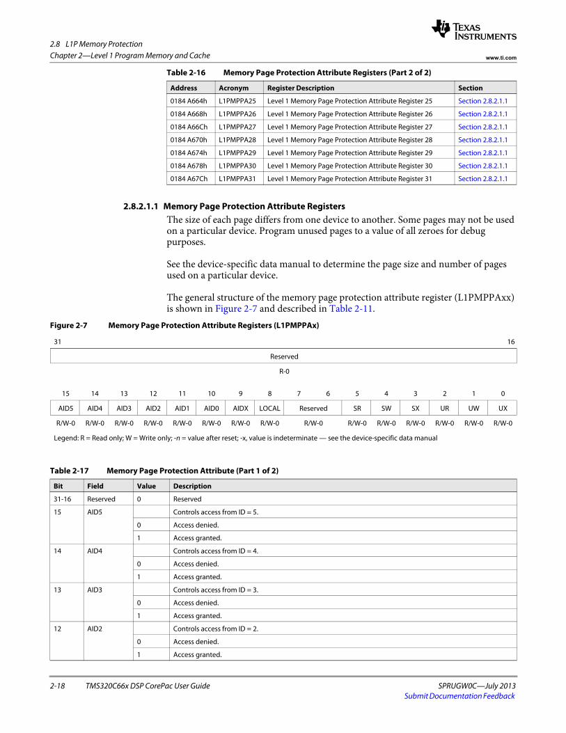
2.8 L1P Memory Protection
2-18 TMS320C66x DSP CorePac User Guide SPRUGW0C—July 2013Submit Documentation Feedback
Chapter 2—Level 1 Program Memory and Cache www.ti.com
2.8.2.1.1 Memory Page Protection Attribute RegistersThe size of each page differs from one device to another. Some pages may not be used on a particular device. Program unused pages to a value of all zeroes for debug purposes.
See the device-specific data manual to determine the page size and number of pages used on a particular device.
The general structure of the memory page protection attribute register (L1PMPPAxx) is shown in Figure 2-7 and described in Table 2-11.
0184 A664h L1PMPPA25 Level 1 Memory Page Protection Attribute Register 25 Section 2.8.2.1.1
0184 A668h L1PMPPA26 Level 1 Memory Page Protection Attribute Register 26 Section 2.8.2.1.1
0184 A66Ch L1PMPPA27 Level 1 Memory Page Protection Attribute Register 27 Section 2.8.2.1.1
0184 A670h L1PMPPA28 Level 1 Memory Page Protection Attribute Register 28 Section 2.8.2.1.1
0184 A674h L1PMPPA29 Level 1 Memory Page Protection Attribute Register 29 Section 2.8.2.1.1
0184 A678h L1PMPPA30 Level 1 Memory Page Protection Attribute Register 30 Section 2.8.2.1.1
0184 A67Ch L1PMPPA31 Level 1 Memory Page Protection Attribute Register 31 Section 2.8.2.1.1
Table 2-16 Memory Page Protection Attribute Registers (Part 2 of 2)
Address Acronym Register Description Section
Figure 2-7 Memory Page Protection Attribute Registers (L1PMPPAx)
31 16
Reserved
R-0
15 14 13 12 11 10 9 8 7 6 5 4 3 2 1 0
AID5 AID4 AID3 AID2 AID1 AID0 AIDX LOCAL Reserved SR SW SX UR UW UX
R/W-0 R/W-0 R/W-0 R/W-0 R/W-0 R/W-0 R/W-0 R/W-0 R/W-0 R/W-0 R/W-0 R/W-0 R/W-0 R/W-0 R/W-0
Legend: R = Read only; W = Write only; -n = value after reset; -x, value is indeterminate — see the device-specific data manual
Table 2-17 Memory Page Protection Attribute (Part 1 of 2)
Bit Field Value Description
31-16 Reserved 0 Reserved
15 AID5 Controls access from ID = 5.
0 Access denied.
1 Access granted.
14 AID4 Controls access from ID = 4.
0 Access denied.
1 Access granted.
13 AID3 Controls access from ID = 3.
0 Access denied.
1 Access granted.
12 AID2 Controls access from ID = 2.
0 Access denied.
1 Access granted.

2.8 L1P Memory Protection
SPRUGW0C—July 2013 TMS320C66x DSP CorePac User Guide 2-19Submit Documentation Feedback
Chapter 2—Level 1 Program Memory and Cachewww.ti.com
2.8.2.2 Memory Protection Lock RegistersIn C66x CorePac, one common set of Memory Protection Lock registers controls the write access to the L1P, L1D and L2 memory protection registers. See Chapter 10 on page 10-9 for information about the Memory Protection Lock registers.
11 AID1 Controls access from ID = 1.
0 Access denied.
1 Access granted.
10 AID0 Controls access from ID = 0.
0 Access denied.
1 Access granted.
9 AIDX Controls access from ID>=6
0 Access denied.
1 Access granted.
8 LOCAL Controls access from PU to local memories (L1/L2)
0 Access denied.
1 Access granted.
7-6 Reserved 0 Reserved.
5 SR Supervisor read access type.
0 Normal operation.
1 Indicates a Supervisor read request.
4 SW Supervisor write access type.
0 Normal operation.
1 Indicates a Supervisor write request.
3 SX Supervisor execute access type.
0 Normal operation.
1 Indicates a Supervisor execute request.
2 UR User read access type.
0 Normal operation.
1 Indicates a User read request.
1 UW User write access type.
0 Normal operation.
1 Indicates a User write request.
0 UX User execute access type.
0 Normal operation.
1 Indicates a User execute request.
Table 2-17 Memory Page Protection Attribute (Part 2 of 2)
Bit Field Value Description

2.8 L1P Memory Protection
2-20 TMS320C66x DSP CorePac User Guide SPRUGW0C—July 2013Submit Documentation Feedback
Chapter 2—Level 1 Program Memory and Cache www.ti.com
2.8.2.3 Memory Protection Fault RegistersTable 2-18 lists the registers for the memory protection fault. See the device-specific data manual for the memory address of these registers.
In order to allow programs to diagnose a memory protection fault after an exception occurs, the L1P implements two registers dedicated to storing information about the fault.
2.8.2.3.1 L1P Memory Protection Fault Address Register (L1PMPFAR)The memory protection fault address register (L1PMPFAR) is shown in Figure 2-8 and described in Table 2-19.
2.8.2.3.2 L1P Memory Protection Fault Set Register (L1PMPFSR)The memory protection fault set register (L1PMPFSR) is shown in Figure 2-9 and described in Table 2-20.
Table 2-18 Memory Protection Fault Registers
Address Acronym Register Description Section
0184 A400h L1PMPFAR Level 1 Program Memory Fault Address Register 2.9.2.3.1
0184 A404h L1PMPFSR Level 1 Program Memory Fault Set Register 2.9.2.3.2
0184 A408h L1PMPFCLR Level 1 Program Memory Fault Clear Register 2.9.2.3.3
Figure 2-8 L1P Memory Protection Fault Address Register (L1PMPFAR)
31 0
Fault Address
R-x
Legend: R = Read only; W = Write only; -n = value after reset; -x, value is indeterminate — see the device-specific data manual
Table 2-19 L1P Memory Protection Fault Address Register (L1PMPFAR) Field Descriptions
Bit Field Value Description
31-0 Fault Address 0-FFFF FFFFh Reserved
Figure 2-9 L1P Memory Protection Fault Set Register (L1PMPFSR)
31 16 15 9 8 7 6 5 4 3 2 1 0
Reserved FID LOCAL Reserved SR SW Reserved UR UW Reserved
R-0 R-0 R-0 R-0 R-0 R-0 R-0 R-0 R-0 R-0
Legend: R = Read only; W = Write only; -n = value after reset; -x, value is indeterminate — see the device-specific data manual
Table 2-20 L1P Memory Protection Fault Set Register (L1PMPFSR) Field Descriptions (Part 1 of 2)
Bit Field Value Description
31-16 Reserved 0 Reserved
15-9 FID 0-7Fh Bit 6:0 of faulting requestor. If ID is narrower than 7 bits, the remaining bits return 0. If ID is wider than 7 bits, the additional bits get truncated. FID =0 if LOCAL =1.
8 LOCAL
0 Normal operation.
1 Access was a "LOCAL" access.
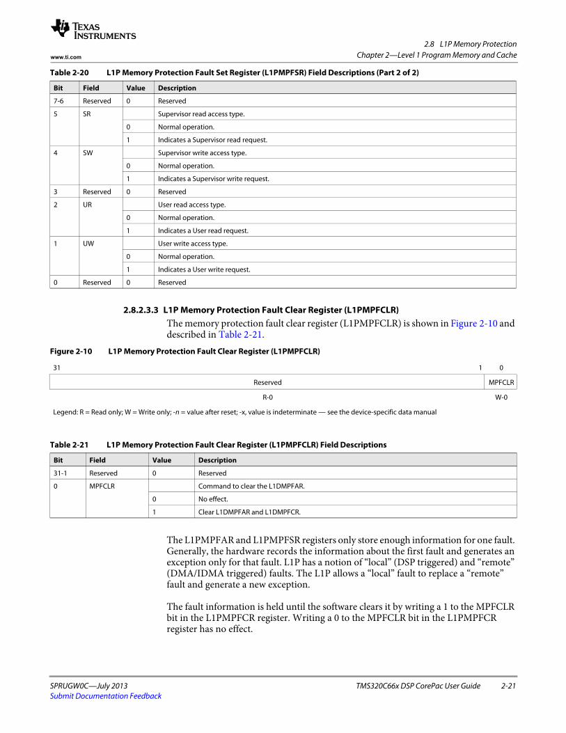
2.8 L1P Memory Protection
SPRUGW0C—July 2013 TMS320C66x DSP CorePac User Guide 2-21Submit Documentation Feedback
Chapter 2—Level 1 Program Memory and Cachewww.ti.com
2.8.2.3.3 L1P Memory Protection Fault Clear Register (L1PMPFCLR)The memory protection fault clear register (L1PMPFCLR) is shown in Figure 2-10 and described in Table 2-21.
The L1PMPFAR and L1PMPFSR registers only store enough information for one fault. Generally, the hardware records the information about the first fault and generates an exception only for that fault. L1P has a notion of “local” (DSP triggered) and “remote” (DMA/IDMA triggered) faults. The L1P allows a “local” fault to replace a “remote” fault and generate a new exception.
The fault information is held until the software clears it by writing a 1 to the MPFCLR bit in the L1PMPFCR register. Writing a 0 to the MPFCLR bit in the L1PMPFCR register has no effect.
7-6 Reserved 0 Reserved
5 SR Supervisor read access type.
0 Normal operation.
1 Indicates a Supervisor read request.
4 SW Supervisor write access type.
0 Normal operation.
1 Indicates a Supervisor write request.
3 Reserved 0 Reserved
2 UR User read access type.
0 Normal operation.
1 Indicates a User read request.
1 UW User write access type.
0 Normal operation.
1 Indicates a User write request.
0 Reserved 0 Reserved
Table 2-20 L1P Memory Protection Fault Set Register (L1PMPFSR) Field Descriptions (Part 2 of 2)
Bit Field Value Description
Figure 2-10 L1P Memory Protection Fault Clear Register (L1PMPFCLR)
31 1 0
Reserved MPFCLR
R-0 W-0
Legend: R = Read only; W = Write only; -n = value after reset; -x, value is indeterminate — see the device-specific data manual
Table 2-21 L1P Memory Protection Fault Clear Register (L1PMPFCLR) Field Descriptions
Bit Field Value Description
31-1 Reserved 0 Reserved
0 MPFCLR Command to clear the L1DMPFAR.
0 No effect.
1 Clear L1DMPFAR and L1DMPFCR.
2.8 L1P Memory Protection
2-22 TMS320C66x DSP CorePac User Guide SPRUGW0C—July 2013Submit Documentation Feedback
Chapter 2—Level 1 Program Memory and Cache www.ti.com
2.8.2.3.4 Protection Checks on Accesses to Memory Protection RegistersL1P implements permission checks on the memory protection registers themselves. The rules are as follows:
• All requestors can read any L1P memory protection (L1PMP) register at any time in all circumstances
• Supervisor can write the register.
Table 2-22 summarizes which L1P memory protection registers are accessible by role and what protection checks are performed in the C66x CorePac. Table 2-22 Permissions for L1P Memory Protection Registers
Register Supervisor User
L1PMPFAR R R
L1PMPFSR R R
L1PMPFCR W /
L1PMPPAxx R/W R
SPRUGW0C—July 2013 TMS320C66x DSP CorePac User Guide 3-1Submit Documentation Feedback
Chapter 3
Level 1 Data Memory and Cache
3.1 "Introduction" on page 3-2 3.2 "L1D Memory Architecture" on page 3-2 3.3 "L1D Cache" on page 3-2 3.4 "L1D Cache Control Registers" on page 3-12 3.5 "L1D Memory Performance " on page 3-18 3.6 "L1D Power-Down Support " on page 3-22 3.7 "L1D Memory Protection" on page 3-23
3.1 Introduction
3-2 TMS320C66x DSP CorePac User Guide SPRUGW0C—July 2013Submit Documentation Feedback
Chapter 3—Level 1 Data Memory and Cache www.ti.com
3.1 Introduction3.1.1 Purpose of the Level 1 Data (L1D) Memory and Cache
The purpose of the L1D memory and cache is to maximize performance of the data processing. The configurability of the L1D memory and cache offers the flexibility to use L1D cache or L1D memory in a system.
3.1.2 FeaturesThe L1D memory and cache provide the following features:
• Configurable L1D cache size: 0K, 4K, 8K, 16K, 32K• Memory protection• Cache block and global coherence operations
3.1.3 Terms and DefinitionsSee Appendix A on page A-1 and Appendix B on page B-1 of this document for detailed definitions of the terms used in this chapter. Appendix A on page A-1 describes general terms used throughout this reference guide and Appendix B on page B-1 defines terms related to the memory and cache architecture.
3.2 L1D Memory Architecture3.2.1 L1D Memory
The L1D memory supports up to 128 Kbytes of memory-mapped RAM. L1D memory cannot be cached within L1D cache, L1P cache, or L2 cache within the same C66x CorePac.
The L1D memory's base address is constrained to 1MB boundaries. The total size of L1D memory must be a multiple of 16K bytes.
The actual memory configuration is device-specific. See the device-specific data sheet for more information.
3.3 L1D CacheThe C66x L1D memory and cache architecture allow converting part or all of L1D into a read-allocate, writeback, two-way set-associative cache. The cache is necessary to facilitate reading and writing data at the full DSP clock rate, while still having a large system memory. It is the cache's responsibility to hide much of the latency associated with reading from and writing to the slower system memory.
The cache controller design supports a range of cache sizes, from 4K through 32K. However, a given device may implement less than 32K of L1D RAM.
The L1D cache converts L1D memory to cache starting at the highest L1D memory address in L1D and working downwards.
The L1D memory is initialized as either “All RAM” or “maximal cache” at reset. See the device-specific data manual for specific behavior.
The operation of the L1D Cache is controlled through several registers. These registers are described in more detail in Section 3.4.

3.3 L1D Cache
SPRUGW0C—July 2013 TMS320C66x DSP CorePac User Guide 3-3Submit Documentation Feedback
Chapter 3—Level 1 Data Memory and Cachewww.ti.com
3.3.1 L1D Cache Architecture L1D cache is a two-way set associative cache, meaning that every physical memory location in the system has two possible locations in the cache where it can reside. When the DSP attempts to access a piece of data, the L1D cache must check whether the requested address resides in either way of the L1D cache. To do so, the 32-bit address provided by the DSP is partitioned into six fields, as shown in Figure 3-1.
The offset of six bits accounts for the fact that an L1D line size is 64 bytes. The cache control logic ignores bits 0 through 5 of the address (the byte, bank, and sub-line fields). Bits 0 through 5 only determine which bank and which bytes within a bank to access; thus, they are irrelevant to the cache's tag compare logic. The set field indicates that the L1D cache line address where the data would reside, if it were cached. The width of the set field depends on the amount of L1D that you configure as cache, as defined in Table 3-1 below. Use the set field to look up and check the tags in each way for any already-cached data from that address as well as the valid bit, which indicates whether the address in the tag actually represents a valid address held in cache.
The tag field is the upper portion of the address that identifies the true physical location of the data element. The cache compares the tag to the stored tags for both ways of the L1D cache.
If one of the tags matches and you set the corresponding valid bit is set on reads, then it is a “hit,” and the data cache returns data to the DSP directly from the L1D cache. Otherwise, the read is a “miss”, and the DSP stalls while the request is sent on to the Level 2 (L2) memory to fetch the data from its location elsewhere in the system.
The DSP can also write data to L1D. When the DSP performs a store, the L1D performs the same tag comparison as it does for reads. If a valid matching tag is found, then the write is a “hit”, and the data is written directly into the L1D cache location. Otherwise, the write is a “miss” and the data is queued in the L1D write buffer. This buffer is used to prevent DSP stalls on write misses. Since the DSP does not wait for data to return on writes, there is no reason to stall during the L2 access.
The L1D cache configuration determines the size of the set and tag fields, as shown in Table 3-1.
Figure 3-1 Data Access Address Organization
31 X+1 X 6 5 4 2 1 0
Tag Set Offset
Sub-line Bank Byte
Legend: R = Read only; W = Write only; -n = value after reset; -x, value is indeterminate — see the device-specific data manual
Table 3-1 Data Access Address Set Field Width (Part 1 of 2)
L1DMODE Setting in the L1DCFG Register Amount of L1D Cache 'X' Bit Position Description
000b 0K N/A L1D is all RAM
001b 4K 10 32 L1D cache lines
010b 8K 11 64 L1D cache lines
011b 16K 12 128 L1D cache lines
100b 32K 13 256 L1D cache lines
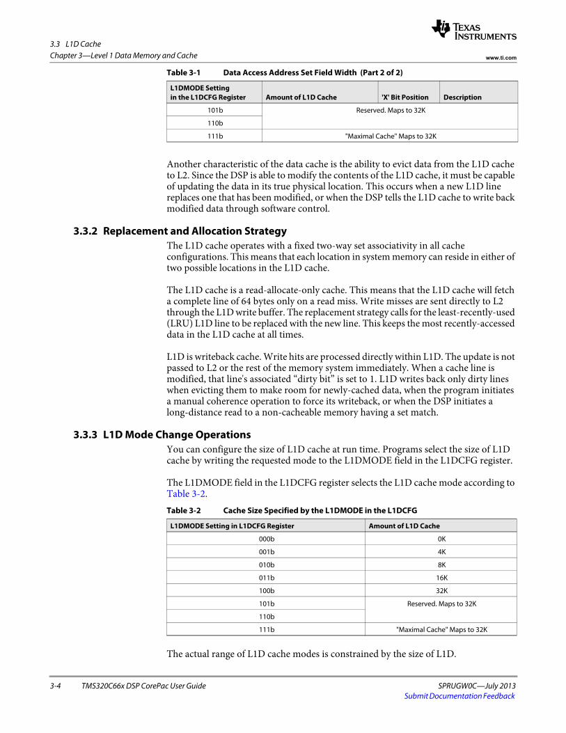
3.3 L1D Cache
3-4 TMS320C66x DSP CorePac User Guide SPRUGW0C—July 2013Submit Documentation Feedback
Chapter 3—Level 1 Data Memory and Cache www.ti.com
Another characteristic of the data cache is the ability to evict data from the L1D cache to L2. Since the DSP is able to modify the contents of the L1D cache, it must be capable of updating the data in its true physical location. This occurs when a new L1D line replaces one that has been modified, or when the DSP tells the L1D cache to write back modified data through software control.
3.3.2 Replacement and Allocation Strategy The L1D cache operates with a fixed two-way set associativity in all cache configurations. This means that each location in system memory can reside in either of two possible locations in the L1D cache.
The L1D cache is a read-allocate-only cache. This means that the L1D cache will fetch a complete line of 64 bytes only on a read miss. Write misses are sent directly to L2 through the L1D write buffer. The replacement strategy calls for the least-recently-used (LRU) L1D line to be replaced with the new line. This keeps the most recently-accessed data in the L1D cache at all times.
L1D is writeback cache. Write hits are processed directly within L1D. The update is not passed to L2 or the rest of the memory system immediately. When a cache line is modified, that line's associated “dirty bit” is set to 1. L1D writes back only dirty lines when evicting them to make room for newly-cached data, when the program initiates a manual coherence operation to force its writeback, or when the DSP initiates a long-distance read to a non-cacheable memory having a set match.
3.3.3 L1D Mode Change OperationsYou can configure the size of L1D cache at run time. Programs select the size of L1D cache by writing the requested mode to the L1DMODE field in the L1DCFG register.
The L1DMODE field in the L1DCFG register selects the L1D cache mode according to Table 3-2.
The actual range of L1D cache modes is constrained by the size of L1D.
101b Reserved. Maps to 32K
110b
111b "Maximal Cache" Maps to 32K
Table 3-1 Data Access Address Set Field Width (Part 2 of 2)
L1DMODE Setting in the L1DCFG Register Amount of L1D Cache 'X' Bit Position Description
Table 3-2 Cache Size Specified by the L1DMODE in the L1DCFG
L1DMODE Setting in L1DCFG Register Amount of L1D Cache
000b 0K
001b 4K
010b 8K
011b 16K
100b 32K
101b Reserved. Maps to 32K
110b
111b "Maximal Cache" Maps to 32K
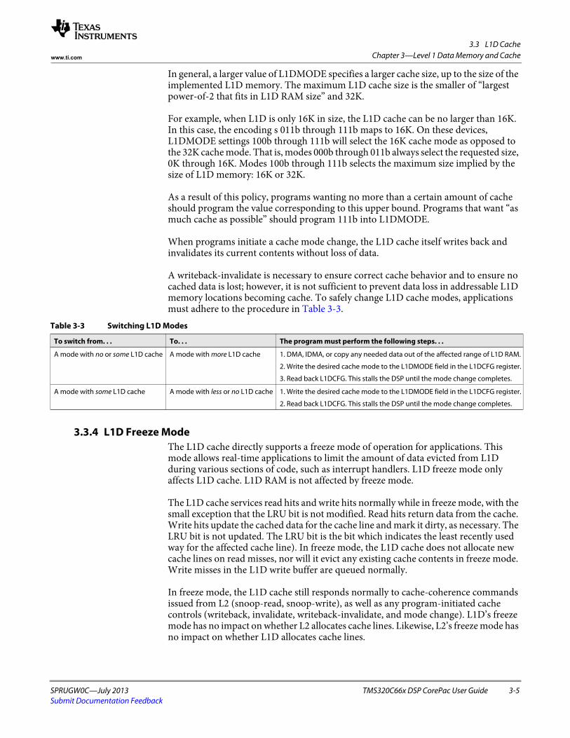
3.3 L1D Cache
SPRUGW0C—July 2013 TMS320C66x DSP CorePac User Guide 3-5Submit Documentation Feedback
Chapter 3—Level 1 Data Memory and Cachewww.ti.com
In general, a larger value of L1DMODE specifies a larger cache size, up to the size of the implemented L1D memory. The maximum L1D cache size is the smaller of “largest power-of-2 that fits in L1D RAM size” and 32K.
For example, when L1D is only 16K in size, the L1D cache can be no larger than 16K. In this case, the encoding s 011b through 111b maps to 16K. On these devices, L1DMODE settings 100b through 111b will select the 16K cache mode as opposed to the 32K cache mode. That is, modes 000b through 011b always select the requested size, 0K through 16K. Modes 100b through 111b selects the maximum size implied by the size of L1D memory: 16K or 32K.
As a result of this policy, programs wanting no more than a certain amount of cache should program the value corresponding to this upper bound. Programs that want “as much cache as possible” should program 111b into L1DMODE.
When programs initiate a cache mode change, the L1D cache itself writes back and invalidates its current contents without loss of data.
A writeback-invalidate is necessary to ensure correct cache behavior and to ensure no cached data is lost; however, it is not sufficient to prevent data loss in addressable L1D memory locations becoming cache. To safely change L1D cache modes, applications must adhere to the procedure in Table 3-3.
3.3.4 L1D Freeze ModeThe L1D cache directly supports a freeze mode of operation for applications. This mode allows real-time applications to limit the amount of data evicted from L1D during various sections of code, such as interrupt handlers. L1D freeze mode only affects L1D cache. L1D RAM is not affected by freeze mode.
The L1D cache services read hits and write hits normally while in freeze mode, with the small exception that the LRU bit is not modified. Read hits return data from the cache. Write hits update the cached data for the cache line and mark it dirty, as necessary. The LRU bit is not updated. The LRU bit is the bit which indicates the least recently used way for the affected cache line). In freeze mode, the L1D cache does not allocate new cache lines on read misses, nor will it evict any existing cache contents in freeze mode. Write misses in the L1D write buffer are queued normally.
In freeze mode, the L1D cache still responds normally to cache-coherence commands issued from L2 (snoop-read, snoop-write), as well as any program-initiated cache controls (writeback, invalidate, writeback-invalidate, and mode change). L1D’s freeze mode has no impact on whether L2 allocates cache lines. Likewise, L2’s freeze mode has no impact on whether L1D allocates cache lines.
Table 3-3 Switching L1D Modes
To switch from. . . To. . . The program must perform the following steps. . .
A mode with no or some L1D cache A mode with more L1D cache 1. DMA, IDMA, or copy any needed data out of the affected range of L1D RAM.
2. Write the desired cache mode to the L1DMODE field in the L1DCFG register.
3. Read back L1DCFG. This stalls the DSP until the mode change completes.
A mode with some L1D cache A mode with less or no L1D cache 1. Write the desired cache mode to the L1DMODE field in the L1DCFG register.
2. Read back L1DCFG. This stalls the DSP until the mode change completes.

3.3 L1D Cache
3-6 TMS320C66x DSP CorePac User Guide SPRUGW0C—July 2013Submit Documentation Feedback
Chapter 3—Level 1 Data Memory and Cache www.ti.com
The OPER field in the L1DCC register controls the L1D freeze mode. The DSP places L1D into freeze mode by writing 1 to the OPER field. The DSP returns L1D to normal operation by writing 0 to the OPER field in the L1DCC register.
The POPER field in the L1DCC register holds the previous value of the OPER field. The value of OPER in the L1DCC register is copied to the POPER field in the L1DCC register on writes to the L1DCC register. This alleviates the cycle cost of reading the L1DCC register (in order to save OPER's previous value) before it is written. If the POPER field is not in the L1DCC register, the program must read, write, and then read again to fully freeze the cache while recording its previous operating mode. If the POPER field is in the L1DCC register, this operation only requires a single write followed by a read.
The following operations occur when you perform a write to the L1DCC register:1. The content of the OPER field copies to the POPER field in the L1DCC register.2. The POPER field loses its previous value.3. The OPER field updates according to the value that the DSP writes to bit 0 of the
L1DCC register. Thus, the write to the L1DCC register only modifies the OPER field in the L1DCC register.
In order to ensure that the L1PCC register updates, the software must perform a write to the L1PCC register followed by a read of the L1PCC register. This guarantees that the requested mode is in effect.
Programs cannot directly modify the POPER field with a single write.
The goal of the OPER and the POPER fields in the L1DCC register is to avoid the DSP cycle penalty and code size involved in a read-write-reread sequence that would otherwise be necessary. Thus, applications may quickly freeze L1D and record the previous “freeze” state of L1D with the short sequence of code in Example 3-1.
Example 3-1 L1D Quick Freeze Example Code Sequence
MVKL L1DCC, A0 ; Point to L1DCCMVKH L1DCC, A0 ;
|| MVK 1, B0 ; OPER encoding for 'freeze'
STW B0, *A0[0] ; Write 1 to L1DCC.OPERLDW *A0[0], A1 ; Read L1DCC to get L1DCC.POPERNOP 4; At this point, L1D is frozen, and the DSP has the old OPER value ; in bit 16 of A1.
End of Example 3-1
You can use the L1DCC register for unfreezing the cache in a manner similar to how it was frozen. Example 3-2 illustrates the code sequence.Example 3-2 L1DCC.OPER Restore Example Code Sequence
MVKL L1DCC, A0 ; Point to L1DCCMVKH L1DCC, A0 ;
|| SHRU A1, 16, A1 ; Shift POPER field into OPER's position
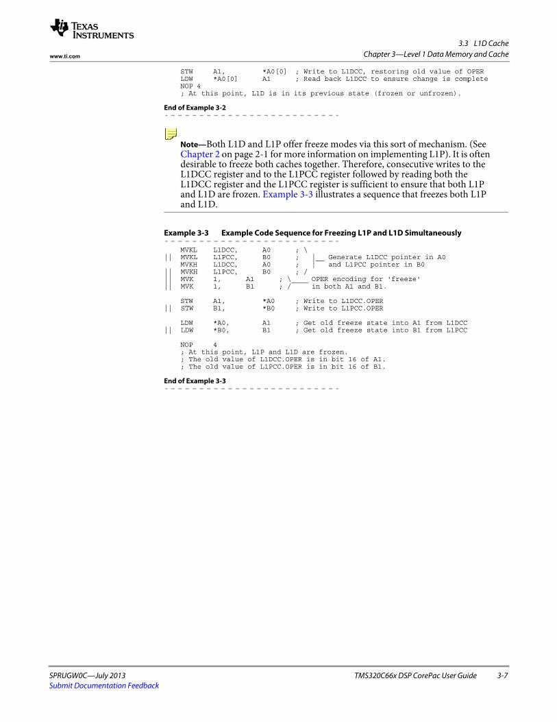
3.3 L1D Cache
SPRUGW0C—July 2013 TMS320C66x DSP CorePac User Guide 3-7Submit Documentation Feedback
Chapter 3—Level 1 Data Memory and Cachewww.ti.com
STW A1, *A0[0] ; Write to L1DCC, restoring old value of OPERLDW *A0[0] A1 ; Read back L1DCC to ensure change is completeNOP 4; At this point, L1D is in its previous state (frozen or unfrozen).
End of Example 3-2
Note—Both L1D and L1P offer freeze modes via this sort of mechanism. (See Chapter 2 on page 2-1 for more information on implementing L1P). It is often desirable to freeze both caches together. Therefore, consecutive writes to the L1DCC register and to the L1PCC register followed by reading both the L1DCC register and the L1PCC register is sufficient to ensure that both L1P and L1D are frozen. Example 3-3 illustrates a sequence that freezes both L1P and L1D.
Example 3-3 Example Code Sequence for Freezing L1P and L1D Simultaneously
MVKL L1DCC, A0 ; \|| MVKL L1PCC, B0 ; |__ Generate L1DCC pointer in A0
MVKH L1DCC, A0 ; | and L1PCC pointer in B0|| MVKH L1PCC, B0 ; /|| MVK 1, A1 ; \____ OPER encoding for 'freeze'|| MVK 1, B1 ; / in both A1 and B1.
STW A1, *A0 ; Write to L1DCC.OPER|| STW B1, *B0 ; Write to L1PCC.OPER
LDW *A0, A1 ; Get old freeze state into A1 from L1DCC|| LDW *B0, B1 ; Get old freeze state into B1 from L1PCC
NOP 4; At this point, L1P and L1D are frozen. ; The old value of L1DCC.OPER is in bit 16 of A1. ; The old value of L1PCC.OPER is in bit 16 of B1.
End of Example 3-3

3.3 L1D Cache
3-8 TMS320C66x DSP CorePac User Guide SPRUGW0C—July 2013Submit Documentation Feedback
Chapter 3—Level 1 Data Memory and Cache www.ti.com
3.3.5 Program-Initiated Cache Coherence OperationsThe C66x L1D cache supports program-initiated cache coherence operations. These operations operate either on a block of addresses, or on the entire L1D cache.
The following cache coherence operations are supported: • Invalidation: Valid cache lines are made invalid. Content of the affected cache
lines is discarded. • Writeback: The content of all dirty cache lines is written to a lower-level memory. • Writeback-invalidation: Writeback operation followed by invalidation. Only the
content of the dirty cache lines is written to lower-level memory, but all of the lines are invalidated.
3.3.5.1 Global Coherence OperationsGlobal cache operations execute on the entire L1D cache. The global coherence operations supported are invalidation, writeback, and writeback-invalidation.
In order to initiate a global invalidation operation, the program must write a 1 to the I bit of the L1DINV register.
Upon completion of the global invalidate operation, the I bit of the L1DINV register resets to 0. The program can poll this bit to detect the completion of the operation.
In order to initiate a global writeback operation, the program needs to write a 1 to the C bit of the L1DWB register.
The C bit of the L1DWB register resets to 0 upon completion. The program can poll this bit to detect the completion of the operation.
The writeback-invalidation operation is controlled in a similar way. In order to initiate a global writeback-invalidation operation, the program must write a 1 to the C bit of the L1DWBINV register.
Table 3-4 provides a summary of the L1D global cache coherence operations.
CAUTION—The L1D global-invalidate causes all updated data in L1D to be discarded, rather than written back to the lower levels of memory. This can cause incorrect operation in programs that expect the updates to be written to the lower levels of memory. Therefore, most programs use either the L1D block writeback-invalidate (described in Section 3.3.5.2) or the global L2 operations, rather than the L1D global-invalidate.
Table 3-4 Global Coherence Operations
Cache Operation Register Used L1D Effect
L1D Writeback L1DWB All updated data written back to L2 / external, but left valid on L1D.
L1D Writeback withInvalidate
L1DWBINV All updated data written back to L2 / external. All lines invalidated within L1D.
L1D Invalidate L1DINV All lines invalidated in L1D. Updated data is dropped.

3.3 L1D Cache
SPRUGW0C—July 2013 TMS320C66x DSP CorePac User Guide 3-9Submit Documentation Feedback
Chapter 3—Level 1 Data Memory and Cachewww.ti.com
You can also globally invalidate the L1D cache by setting the ID bit in the L2CFG register to 1 for legacy reasons. The ID field is provided for backward compatibility with C64x devices, but it should not be used in new applications. New applications should use the L1DINV register.
3.3.5.2 Block Coherence OperationsBlock coherence operations have similar functionality as the global coherence operations; however, they apply only to a defined block of data. This block is defined by the base address and by the word (32-bit) size in the associated memory-mapped registers.
The block coherence operations supported are invalidation, writeback, and writeback-invalidation. Each operation has two registers associated with it. The L1DXXBAR register defines the base address of the block and the L1DXXWC register defines the word size of the block.
Writing a non-zero value to the word count field in the L1DXXWC register initiates a block coherence operation. The word count field sets to 0 upon completion of the block coherence operation. The program can poll this field to detect the completion of the operation.
On the C66x DSP, it is recommended that programs wait for block coherence operations to complete before continuing. To issue a block coherence operation:
1. Write the starting address to the L1DXXBAR register.2. Write the word count to the L1DXXWC register.3. Wait for completion by one of the following methods:
a. Issue an MFENCE instruction (preferred), orb. Poll the L1DXXWC register until the word count field reads as zero.
The MFENCE instruction is new to the C66x DSP. It stalls the DSP until all outstanding memory operations complete. For further information about MFENCE instruction, see the C66x DSP and Instruction Set Reference Guide (SPRUGH7) in ‘‘Related Documentation from Texas Instruments’’ on page ø-xx.
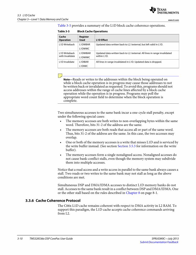
3.3 L1D Cache
3-10 TMS320C66x DSP CorePac User Guide SPRUGW0C—July 2013Submit Documentation Feedback
Chapter 3—Level 1 Data Memory and Cache www.ti.com
Table 3-5 provides a summary of the L1D block cache coherence operations.
Note—Reads or writes to the addresses within the block being operated on while a block cache operation is in progress may cause those addresses to not be written back or invalidated as requested. To avoid this, programs should not access addresses within the range of cache lines affected by a block cache operation while the operation is in progress. Programs may poll the appropriate word count field to determine when the block operation is complete.
Two simultaneous accesses to the same bank incur a one-cycle stall penalty, except under the following special cases:
• The memory accesses are both writes to non-overlapping bytes within the same word. Therefore, bits 31-2 of the address are the same.
• The memory accesses are both reads that access all or part of the same word. Thus, bits 31-2 of the address are the same. In this case, the two accesses may overlap.
• One or both of the memory accesses is a write that misses L1D and is serviced by the write buffer instead. (See section Section 3.5.3 for information on the write buffer).
• The memory accesses form a single nonaligned access. Nonaligned accesses do not cause bank-conflict stalls, even though the memory system may subdivide them into multiple accesses.
Notice that a read access and a write access in parallel to the same bank always causes a stall. Two reads or two writes to the same bank may not stall as long as the above conditions are met.
Simultaneous DSP and DMA/IDMA accesses to distinct L1D memory banks do not stall. Accesses to the same bank result in a conflict between DSP and DMA/IDMA. One or the other stall based on the rules described in Chapter 8 on page 8-1.
3.3.6 Cache Coherence ProtocolThe C66x L1D cache remains coherent with respect to DMA activity in L2 RAM. To support this paradigm, the L1D cache accepts cache coherence commands arriving from L2.
Table 3-5 Block Cache Operations
Cache Operation
Register Used L1D Effect
L1D Writeback L1DWBAR
L1DWWC
Updated data written back to L2 /external, but left valid in L1D.
L1D Writeback with Invalidate
L1DWIBAR
L1DWIWC
Updated data written back to L2 /external. All lines in range invalidated within L1D.
L1D Invalidate L1DIBAR
L1DIWC
All lines in range invalidated in L1D. Updated data is dropped.

3.3 L1D Cache
SPRUGW0C—July 2013 TMS320C66x DSP CorePac User Guide 3-11Submit Documentation Feedback
Chapter 3—Level 1 Data Memory and Cachewww.ti.com
3.3.6.1 L2 to L1D Cache Coherence Protocol To support L1D cache coherence with respect to DMA/IDMA traffic in L2 RAM, the L1D controller supports two cache coherence commands arriving from L2: snoop-read (SNPR) and snoop-write (SNPW). The L2 only sends these snoop commands, when necessary, in response to DMA and IDMA activity in L2 RAM.
Snoop-read is sent to L1D when L2 detects that the L1D cache holds the requested line, and that the line is dirty. L1D responds by returning the requested data.
Snoop-write is sent to L1D when L2 detects that the L1D holds the requested line. It does not matter if the line is modified within L1D. The L1D updates its contents accordingly.
3.3.6.2 L1D to L2 Cache Coherence Protocol In order to reduce excessive snoop traffic to L1D, L2 filters the snoops so that unnecessary snoops are not sent to L1D.
L2 keeps a shadow copy of L1D's tag memory. L2 consults its local copy of the L1D tags to decide whether a snoop command to L1D is warranted.
L2 primarily updates its shadow tags in response to L1D read miss requests, and secondarily in response to L1D victim writebacks. When L1D issues a read request, it also indicates whether or not the line is allocated within L1D; and if so, what way within the set the line is allocated in. L2 can update the corresponding set in its shadow tags from this information.
In addition to tracking which addresses are present in L1D cache, L2 tracks also tracks whether or not those lines are dirty in the C66x DSP.

3.4 L1D Cache Control Registers
3-12 TMS320C66x DSP CorePac User Guide SPRUGW0C—July 2013Submit Documentation Feedback
Chapter 3—Level 1 Data Memory and Cache www.ti.com
3.4 L1D Cache Control Registers3.4.1 Memory Mapped L1D Cache Control Register Overview
The C66x memory system provides a set of registers to govern the operation of L1D cache. These registers allow for changing cache modes and manually initiating cache coherence operations.
Table 3-6 below lists the L1D cache control registers.
In addition to the L1D-specific registers listed above, the L1D cache is directly affected by writes to L2-specific controls as well. See Chapter 4 on page 4-1 for the complete list of cache control operations and their effect on the L1D cache.
3.4.2 L1D Cache Configuration RegistersThe L1DCFG and L1DCC registers control the operation of L1D.
3.4.2.1 L1D Cache Configuration (L1DCFG) RegisterThe L1D cache configuration register (L1DCFG) controls the size of L1D cache and is shown in Figure 3-2 and described in Table 3-7.
Table 3-6 L1D Specific Cache Control Operations
Type of Operation Register Name Address Action Section
Mode Select L1DCFG
L1DCC
0184 0040h
0184 0044h
Configures the size of L1D cache.
Controls L1D operating mode (freeze/normal).
Section 3.4.2.1
Section 3.4.2.2
Block Cache Operation
L1DWIBAR
L1DWIWC
0184 4030h
0184 4034h
Specified range is written back and invalidated within L1D. Section 3.4.3.2
L1DWBAR
L1DWWC
0184 4040h
0184 4044h
Specified range is written back from L1D and left valid.
L1DIBAR
L1DIWC
0184 4048h
0184 404Ch
Specified range is invalidated in L1D without being written back.
Global Cache Operation
L1DWB
L1DWBINV
L1DINV
0184 5040h
0184 5044h
0184 5048h
Entire contents of L1D is written back, but left valid.
Entire contents of L1D is written back and invalidated.
Entire contents of L1D is invalidated without being written back.
Section 3.4.3.1
Figure 3-2 L1D Cache Configuration Register (L1DCFG)
31 3 2 0
Reserved L1DMODE
R-0 R/W-0h or 7h
Legend: R = Read only; W = Write only; -n = value after reset; -x, value is indeterminate — see the device-specific data manual
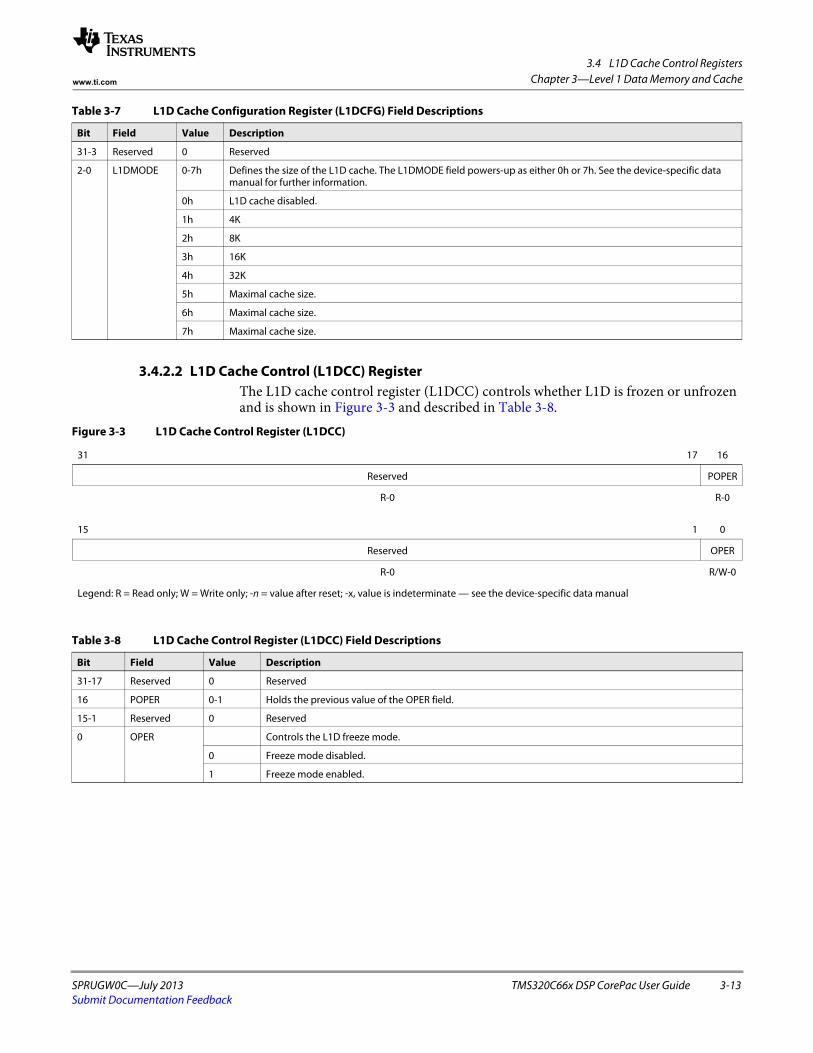
3.4 L1D Cache Control Registers
SPRUGW0C—July 2013 TMS320C66x DSP CorePac User Guide 3-13Submit Documentation Feedback
Chapter 3—Level 1 Data Memory and Cachewww.ti.com
3.4.2.2 L1D Cache Control (L1DCC) RegisterThe L1D cache control register (L1DCC) controls whether L1D is frozen or unfrozen and is shown in Figure 3-3 and described in Table 3-8.
Table 3-7 L1D Cache Configuration Register (L1DCFG) Field Descriptions
Bit Field Value Description
31-3 Reserved 0 Reserved
2-0 L1DMODE 0-7h Defines the size of the L1D cache. The L1DMODE field powers-up as either 0h or 7h. See the device-specific data manual for further information.
0h L1D cache disabled.
1h 4K
2h 8K
3h 16K
4h 32K
5h Maximal cache size.
6h Maximal cache size.
7h Maximal cache size.
Figure 3-3 L1D Cache Control Register (L1DCC)
31 17 16
Reserved POPER
R-0 R-0
15 1 0
Reserved OPER
R-0 R/W-0
Legend: R = Read only; W = Write only; -n = value after reset; -x, value is indeterminate — see the device-specific data manual
Table 3-8 L1D Cache Control Register (L1DCC) Field Descriptions
Bit Field Value Description
31-17 Reserved 0 Reserved
16 POPER 0-1 Holds the previous value of the OPER field.
15-1 Reserved 0 Reserved
0 OPER Controls the L1D freeze mode.
0 Freeze mode disabled.
1 Freeze mode enabled.
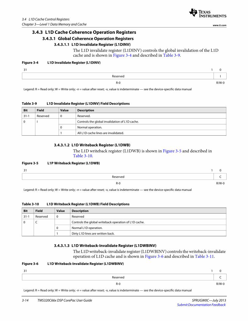
3.4 L1D Cache Control Registers
3-14 TMS320C66x DSP CorePac User Guide SPRUGW0C—July 2013Submit Documentation Feedback
Chapter 3—Level 1 Data Memory and Cache www.ti.com
3.4.3 L1D Cache Coherence Operation Registers3.4.3.1 Global Coherence Operation Registers
3.4.3.1.1 L1D Invalidate Register (L1DINV)The L1D invalidate register (L1DINV) controls the global invalidation of the L1D cache and is shown in Figure 3-4 and described in Table 3-9.
3.4.3.1.2 L1D Writeback Register (L1DWB)The L1D writeback register (L1DWB) is shown in Figure 3-5 and described in Table 3-10.
3.4.3.1.3 L1D Writeback-Invalidate Register (L1DWBINV)The L1D writeback-invalidate register (L1DWBINV) controls the writeback-invalidate operation of L1D cache and is shown in Figure 3-6 and described in Table 3-11.
Figure 3-4 L1D Invalidate Register (L1DINV)
31 1 0
Reserved I
R-0 R/W-0
Legend: R = Read only; W = Write only; -n = value after reset; -x, value is indeterminate — see the device-specific data manual
Table 3-9 L1D Invalidate Register (L1DINV) Field Descriptions
Bit Field Value Description
31-1 Reserved 0 Reserved.
0 I Controls the global invalidation of L1D cache.
0 Normal operation.
1 All L1D cache lines are invalidated.
Figure 3-5 L1P Writeback Register (L1DWB)
31 1 0
Reserved C
R-0 R/W-0
Legend: R = Read only; W = Write only; -n = value after reset; -x, value is indeterminate — see the device-specific data manual
Table 3-10 L1D Writeback Register (L1DWB) Field Descriptions
Bit Field Value Description
31-1 Reserved 0 Reserved
0 C Controls the global writeback operation of L1D cache.
0 Normal L1D operation.
1 Dirty L1D lines are written back.
Figure 3-6 L1D Writeback-Invalidate Register (L1DWBINV)
31 1 0
Reserved C
R-0 R/W-0
Legend: R = Read only; W = Write only; -n = value after reset; -x, value is indeterminate — see the device-specific data manual

3.4 L1D Cache Control Registers
SPRUGW0C—July 2013 TMS320C66x DSP CorePac User Guide 3-15Submit Documentation Feedback
Chapter 3—Level 1 Data Memory and Cachewww.ti.com
3.4.3.2 Block Coherence Operation Registers3.4.3.2.1 L1D Invalidate Base Address Register (L1DIBAR)
The L1D invalidate base address register (L1DIBAR) defines the base address of the block that will be invalidated and is shown in Figure 3-7 and described in Table 3-12.
3.4.3.2.2 L1D Invalidate Word Count Register (L1DIWC) The L1D invalidate word count register (L1DIWC) defines the size of the block that will be invalidated. The size is defined in 32-bit words and is shown in Figure 3-8 and described in Table 3-13. All Cache Lines touched by the combination of the L1DIBAR Address and the L1D1WC word count will be invalidated.
Table 3-11 L1D Writeback-Invalidate Register (L1DWBINV) Field Descriptions
Bit Field Value Description
31-1 Reserved 0 Reserved
0 C Controls the global writeback-invalidate operation of L1D cache.
0 Normal L1D operation.
1 Dirty L1D lines written back, all L1D lines are invalidated.
Figure 3-7 L1D Invalidate Base Address Register (L1DIBAR)
31 0
L1D Invalidate Base Address (L1DIBAR)
W-x
Legend: R = Read only; W = Write only; -n = value after reset; -x, value is indeterminate — see the device-specific data manual
Table 3-12 L1D Invalidate Base Address Register (L1DIBAR) Field Descriptions
Bit Field Value Description
31-0 L1DIBAR 0-FFFF FFFFh Defines the base address for the L1D block invalidate operation.
Figure 3-8 L1D Invalidate Word Count Register (L1DIWC)
31 16
Reserved
R-0
15 0
L1D Invalidate Word Count (L1DIWC)
R/W-0
Legend: R = Read only; W = Write only; -n = value after reset; -x, value is indeterminate — see the device-specific data manual
Table 3-13 L1D Invalidate Word Count Register (L1DIWC) Field Descriptions
Bit Field Value Description
31-16 Reserved 0 Reserved
15-0 L1DIWC 0-FFFFh Word count for block invalidation
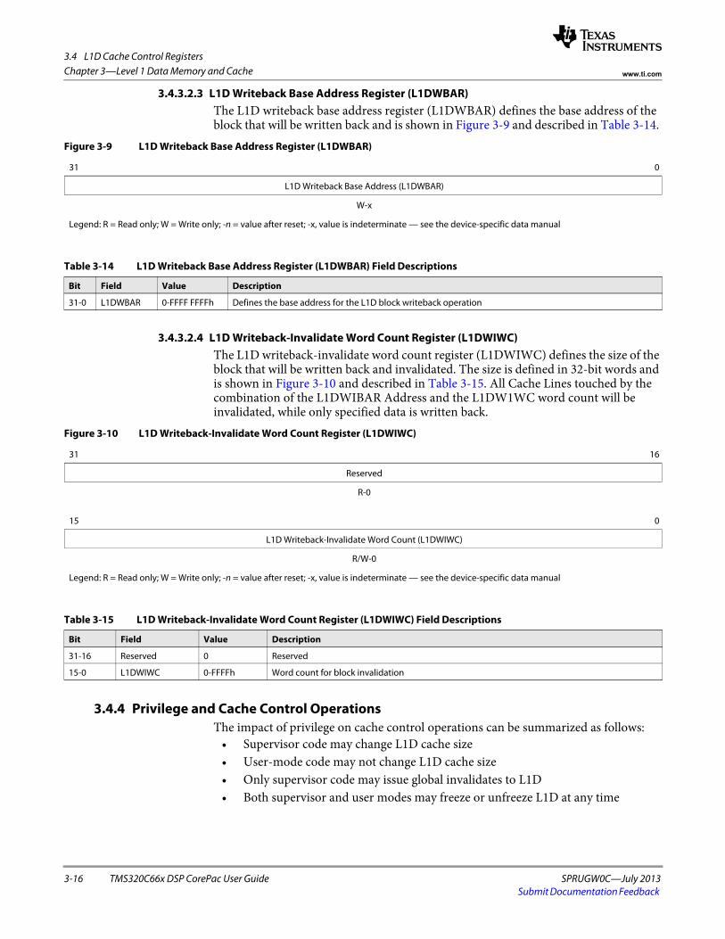
3.4 L1D Cache Control Registers
3-16 TMS320C66x DSP CorePac User Guide SPRUGW0C—July 2013Submit Documentation Feedback
Chapter 3—Level 1 Data Memory and Cache www.ti.com
3.4.3.2.3 L1D Writeback Base Address Register (L1DWBAR)The L1D writeback base address register (L1DWBAR) defines the base address of the block that will be written back and is shown in Figure 3-9 and described in Table 3-14.
3.4.3.2.4 L1D Writeback-Invalidate Word Count Register (L1DWIWC) The L1D writeback-invalidate word count register (L1DWIWC) defines the size of the block that will be written back and invalidated. The size is defined in 32-bit words and is shown in Figure 3-10 and described in Table 3-15. All Cache Lines touched by the combination of the L1DWIBAR Address and the L1DW1WC word count will be invalidated, while only specified data is written back.
3.4.4 Privilege and Cache Control OperationsThe impact of privilege on cache control operations can be summarized as follows:
• Supervisor code may change L1D cache size• User-mode code may not change L1D cache size• Only supervisor code may issue global invalidates to L1D• Both supervisor and user modes may freeze or unfreeze L1D at any time
Figure 3-9 L1D Writeback Base Address Register (L1DWBAR)
31 0
L1D Writeback Base Address (L1DWBAR)
W-x
Legend: R = Read only; W = Write only; -n = value after reset; -x, value is indeterminate — see the device-specific data manual
Table 3-14 L1D Writeback Base Address Register (L1DWBAR) Field Descriptions
Bit Field Value Description
31-0 L1DWBAR 0-FFFF FFFFh Defines the base address for the L1D block writeback operation
Figure 3-10 L1D Writeback-Invalidate Word Count Register (L1DWIWC)
31 16
Reserved
R-0
15 0
L1D Writeback-Invalidate Word Count (L1DWIWC)
R/W-0
Legend: R = Read only; W = Write only; -n = value after reset; -x, value is indeterminate — see the device-specific data manual
Table 3-15 L1D Writeback-Invalidate Word Count Register (L1DWIWC) Field Descriptions
Bit Field Value Description
31-16 Reserved 0 Reserved
15-0 L1DWIWC 0-FFFFh Word count for block invalidation
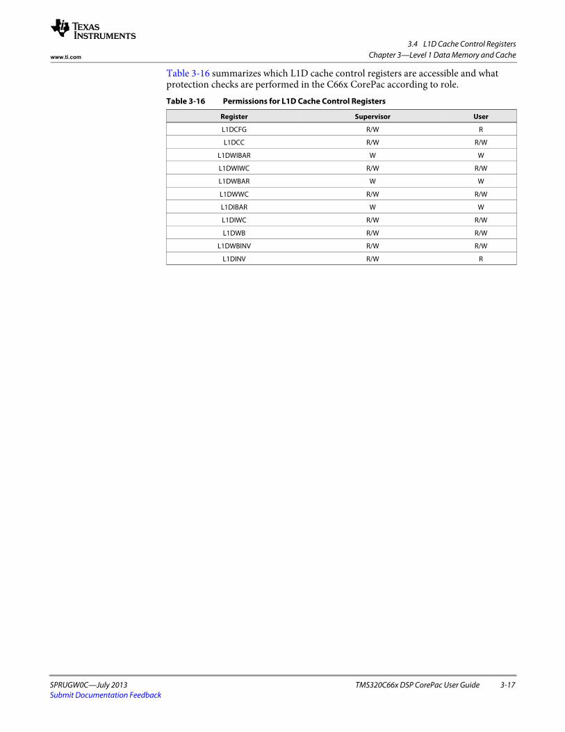
3.4 L1D Cache Control Registers
SPRUGW0C—July 2013 TMS320C66x DSP CorePac User Guide 3-17Submit Documentation Feedback
Chapter 3—Level 1 Data Memory and Cachewww.ti.com
Table 3-16 summarizes which L1D cache control registers are accessible and what protection checks are performed in the C66x CorePac according to role.Table 3-16 Permissions for L1D Cache Control Registers
Register Supervisor User
L1DCFG R/W R
L1DCC R/W R/W
L1DWIBAR W W
L1DWIWC R/W R/W
L1DWBAR W W
L1DWWC R/W R/W
L1DIBAR W W
L1DIWC R/W R/W
L1DWB R/W R/W
L1DWBINV R/W R/W
L1DINV R/W R

3.5 L1D Memory Performance
3-18 TMS320C66x DSP CorePac User Guide SPRUGW0C—July 2013Submit Documentation Feedback
Chapter 3—Level 1 Data Memory and Cache www.ti.com
3.5 L1D Memory Performance The performance of the L1D memory depends on several factors. This section describes the impact of the banking architecture, the write buffer, and the miss pipelining on the performance of the L1D memory.
3.5.1 L1D Memory BankingThe L1D has a least-significant bit (LSB) based memory banking structure that divides memory into eight 32-bit-wide banks. These banks are single-ported, allowing only one access per cycle. L1D RAM and L1D cache both share the same bank structure.
The banks are interleaved based on the low-order bits of the address. Specifically, for aligned memory accesses, address bits [4:2] determine the bank number. The mapping of bits to bank number varies with the device endian mode.
In Figure 3-11, bits 4-2 of the address select the bank and bits 1-0 select the byte within the bank.
The shaded areas in Figure 3-12 show combinations of parallel accesses that may result in bank-conflict stalls according to the LSBs of addresses for the two accesses. Two simultaneous accesses to the same bank incur a one-cycle stall penalty, except under the following special cases:
• The memory accesses are both writes to non-overlapping bytes within the same word. Thus, bits 2 through 31 of the address are the same.
• The memory accesses are both reads that access all or part of the same word. Thus, bits 2 through 31 of the address are the same. In this case, the two accesses may overlap.
• The memory accesses form a single nonaligned access. Nonaligned accesses do not cause bank-conflict stalls, even though the memory system may subdivide them into multiple accesses.
Notice that a read access and a write access in parallel to the same bank always causes a stall. Two reads or two writes to the same bank may not stall as long as the above conditions are met.
DSP and DMA/IDMA accesses to distinct L1D memory banks do not stall. Accesses to the rules same bank results in a conflict between DSP and DMA/IDMA. One or the other stalls based on the rules described in Chapter 8 on page 8-1.
Figure 3-11 Address to Bank Number Mapping
31 16
Upper Address Bits
15 5 4 2 1 0
Upper Address Bits Bank Number Offset
Legend: R = Read only; W = Write only; -n = value after reset; -x, value is indeterminate — see the device-specific data manual

3.5 L1D Memory Performance
SPRUGW0C—July 2013 TMS320C66x DSP CorePac User Guide 3-19Submit Documentation Feedback
Chapter 3—Level 1 Data Memory and Cachewww.ti.com
Figure 3-12 Potentially Conflicting Memory Accesses
3.5.2 L1D Miss PenaltyThe L1D can service up to two data accesses from the DSP every cycle. Accesses that hit L1D complete without stalls, unless a bank conflict occurs as described in Section 3.3.6.1.
Reads that miss L1D stall the DSP while the requested data is fetched. The L1D is a read-allocate cache, and so it will allocate a new line for the requested data.
An L1D read miss that also misses L2 stalls the DSP while the L2 retrieves the data from external memory. Once the data is retrieved, it is stored in L2 and transferred to the L1D. The external miss penalty varies depending on the type and width of external memory used to hold external data, as well as other aspects of system loading.
00000
01
000
10
000
11
000
00
100
11001 1
1 10 0
10
0 0 0
00
010
11001 1
0 01 1
01
0 1 1010 10
1 11 1
1 11 1
0 0 0 0 0 0 0
00
001 1
11
01110
01 1
0 00 0
00
0 1 1010 10
1 10 0
1 10 0
1 1 1 1 1 1 1
0 1010 0
100
101
0 0101 1
0 11 1
11
11 1 1 1 1
11
111
00
000
10
000
00
100
10
100
00
010
10
010
00
110 0
0111
00
001
10
001
00
101
10
101
00
011
10
10
1
00
111
10
111
00
000
00
100
00
010
11
00
0
00
001
00
101
00
011
00
111
00
000
00
10
0
00
001
00
011
Byte Halfword Word DWDA1
000000 0 0 0 10 0 0 1 0
1 10001 0000
0 0 1 0 10 0 1 1 00 0 1 1 10 1 0 0 00 1 0 0 10 1 0 1 00 1 0 1 10 1 1 0 00 1 1 0 10 1 1 1 00 1 1 1 11 0 0 0 0
01 00 11 0 0 01
01 10 11 0 1 0 0
01 01 11 0 1 1 0
01 11 11 1 0 0 0
11 00 11 1 0 1 01 1 0 111 1 1 0 01 1 1 0 11 1 1 1 01 1 1 1 10 0 0 0 0
1 00 0 00 0 1 0 0
100 1 00 001 0
10 0 1 010 1 00
10 1
1 01 0 0 0 0
01 0
1 0
01 0 010111
01 1000
11 0 1 011 01 011 1 1 000 0 0 0
01 00 000 1 0 0
01 1 0001 0 0 0
1 0 01 001 1 0 0
1 1 1 000 00 0 00 01 0 01 000 0
0011 0
Bits4−0
DW
Word
Halfw
ord
Byte
DA
2
3.5 L1D Memory Performance
3-20 TMS320C66x DSP CorePac User Guide SPRUGW0C—July 2013Submit Documentation Feedback
Chapter 3—Level 1 Data Memory and Cache www.ti.com
If there are two read misses to the same line in the same cycle, only one miss penalty is incurred. Similarly, if there are two accesses in succession to the same line and the first one is a miss, the second access does not incur any additional miss penalty.
The process of allocating a line in L1D can result in a victim writeback. Victim writebacks move updated data out of L1D to the lower levels of memory. When updated data is evicted from L1D, the cache moves the data to the victim buffer. Once the data is moved to the victim buffer, the L1D resumes processing of the current read miss. Further processing of the victim writeback occurs in the background. Subsequent read and write misses, however, must wait for the victim writeback to process. If the read misses do not conflict with existing victims, the read misses are pipelined with the victim writebacks in order to reduce the performance penalty.
The L1D pipelines read misses. Consecutive read misses to different lines may overlap, reducing the overall stall penalty.
Write misses do not stall the DSP directly. Write misses are queued in the write buffer that is between L1D and L2. Although the DSP does not always stall for write misses, the write buffer can stall the DSP under various circumstances. Section 3.5.3 describes the effects of the write buffer.
3.5.3 L1D Write BufferThe L1D does not write allocate. Rather, write misses are passed directly to L2 without allocating a line in L1D. A 128-bit wide by 4-entry write buffer exists between the L1D cache and the L2 memory to capture these write misses. The write buffer provides a 128-bit path for writes from L1D to L2 with room for four outstanding write requests.
Writes that miss L1D do not stall the DSP unless the write buffer is full. If the write buffer is full, a write miss can indirectly stall the DSP until there is room in the buffer for the write. The write buffer can also stall the DSP by extending the time for a read miss. Reads that miss L1D are not processed as long as the write buffer is not empty. Once the write buffer empties, the read miss processes. This is necessary as a read miss may overlap an address for which a write is pending in the write buffer.
The L2 can process a new request from the write buffer every L2 cycle (L2 cycle = 2 x DSP cycles), provided that the requested L2 bank is not busy. You can merge multiple elements within a buffer together for a single memory access if they are contiguous in memory to reduce the potential for buffer stalls and DMA contention.
The write buffer allows write requests to merge and merges two write misses into a single transaction, provided that the write request obeys the following rules:
• The new write miss resides within the same 128-bit quad-word as the immediately preceding write miss.
• The two writes are to locations in L2 SRAM (not to locations that may be held in L2 cache)
• The first write has just been placed in the write buffer queue• The second write is presently being placed in the buffer queue• The first write has not yet been presented to the L2 controller• Both writes have the same privilege level
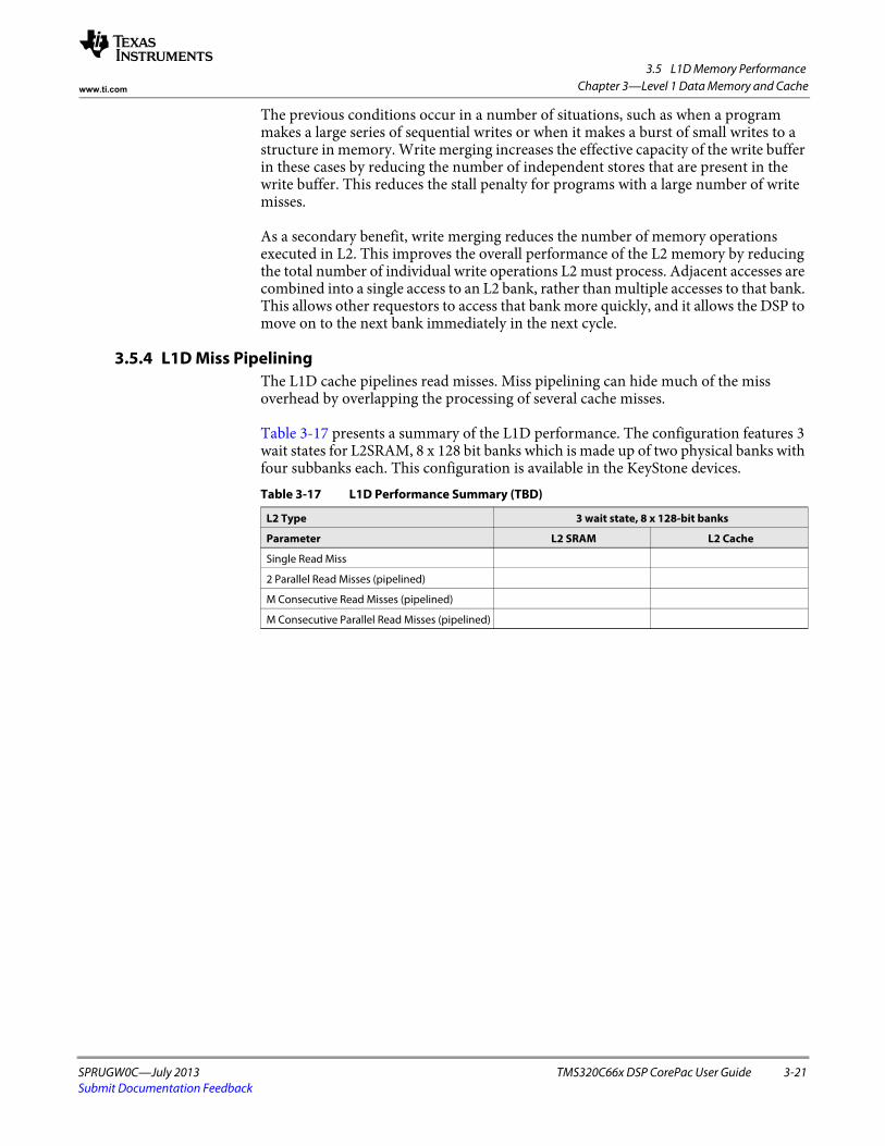
3.5 L1D Memory Performance
SPRUGW0C—July 2013 TMS320C66x DSP CorePac User Guide 3-21Submit Documentation Feedback
Chapter 3—Level 1 Data Memory and Cachewww.ti.com
The previous conditions occur in a number of situations, such as when a program makes a large series of sequential writes or when it makes a burst of small writes to a structure in memory. Write merging increases the effective capacity of the write buffer in these cases by reducing the number of independent stores that are present in the write buffer. This reduces the stall penalty for programs with a large number of write misses.
As a secondary benefit, write merging reduces the number of memory operations executed in L2. This improves the overall performance of the L2 memory by reducing the total number of individual write operations L2 must process. Adjacent accesses are combined into a single access to an L2 bank, rather than multiple accesses to that bank. This allows other requestors to access that bank more quickly, and it allows the DSP to move on to the next bank immediately in the next cycle.
3.5.4 L1D Miss PipeliningThe L1D cache pipelines read misses. Miss pipelining can hide much of the miss overhead by overlapping the processing of several cache misses.
Table 3-17 presents a summary of the L1D performance. The configuration features 3 wait states for L2SRAM, 8 x 128 bit banks which is made up of two physical banks with four subbanks each. This configuration is available in the KeyStone devices.Table 3-17 L1D Performance Summary (TBD)
L2 Type 3 wait state, 8 x 128-bit banks
Parameter L2 SRAM L2 Cache
Single Read Miss
2 Parallel Read Misses (pipelined)
M Consecutive Read Misses (pipelined)
M Consecutive Parallel Read Misses (pipelined)

3.6 L1D Power-Down Support
3-22 TMS320C66x DSP CorePac User Guide SPRUGW0C—July 2013Submit Documentation Feedback
Chapter 3—Level 1 Data Memory and Cache www.ti.com
3.6 L1D Power-Down Support You can set the L1D memory to powered-down mode when the DSP is in idle mode.
The following software sequence is required to power-down the C66x CorePac: 1. Enable power-down by setting the MEGPD field in the PDCCMD register to 1. 2. Enable the DSP interrupt(s) that you want to wake-up the C66x CorePac; disable
all others.3. Execute an IDLE instruction.
The C66x CorePac stays in powered-down mode until the interrupt(s) that you enabled in step 2, above wake them up.
If a DMA access occurs to the L1D, L1P, or L2 memory while the C66x CorePac is powered-down, the power-down controller (PDC) wakes up all three memory controllers. When the DMA access has been serviced, the PDC will power-down the memory controllers again.
See Chapter 12 on page 12-1 for more information about the PDCCMD register and the power-down capabilities of the C66x CorePac.
Note—Powering-down the C66x CorePac as described here is often called static power-down. This term is used to describe this mode since it is often used for longer periods of time.

3.7 L1D Memory Protection
SPRUGW0C—July 2013 TMS320C66x DSP CorePac User Guide 3-23Submit Documentation Feedback
Chapter 3—Level 1 Data Memory and Cachewww.ti.com
3.7 L1D Memory ProtectionL1D memory supports memory protection to offer the robustness required in many systems. Several levels of memory protection are available. Not all the levels are available on all the devices. See the device-specific data manual for more information. Familiarize yourself with Chapter 10 on page 10-1 before you read this section.
3.7.1 Protection Checks on L1D Accesses3.7.1.1 Protection Checks on DSP, IDMA and Other System Master Accesses
Protection checks are performed for all accesses that are serviced directly by the L1D on devices that include memory protection support. This includes accesses from the DSP, IDMA other system master accesses.
The L2 controller determines whether a given DSP request is allowed or disallowed based on the privilege level associated with the request and the permission settings on the address range that the request accesses. The exact rules for these checks are set forth in Chapter 10 on page 10-1.
The L1D memory controllers feature two exception outputs that are routed to the C66x interrupt controller. One of these exception outputs indicates that a DSP-triggered “local” memory exception (L1D_CMPA) occurred. The other indicates that a system master-triggered “remote” exception (L1D_DMPA) occurred.
3.7.1.2 Additional Protection Checks on Program Initiated Cache Coherence OperationsProtection checks are performed on program initiated cache coherence operations to ensure the integrity of the memory protection. Both user and supervisor code may issue manual cache coherence operations.
However, user code cannot globally invalidate L1D cache or change the size of L1D cache. Only supervisor code may initiate a global invalidation or change the amount of memory allocated to cache.
3.7.2 L1D Memory Protection RegistersThe following registers govern the operation of the L1D memory protection. They fall into three main categories:
• Memory Protection Page Attribute Registers (MPPA): These registers store the permissions associated with each protected page.
• Memory Protection Lock Registers (MPLK): Memory Controllers may choose to implement a hardware memory protection lock. When engaged, the lock disables all updates to the memory protection entries for all four memory controllers (L1P, L1D, L2 and XMC).
• Memory Protection Fault Registers (MPFxR): Each memory controller that generates memory protection faults provides the MPFAR, MPFSR, and MPFCR registers with recording the details of the fault.
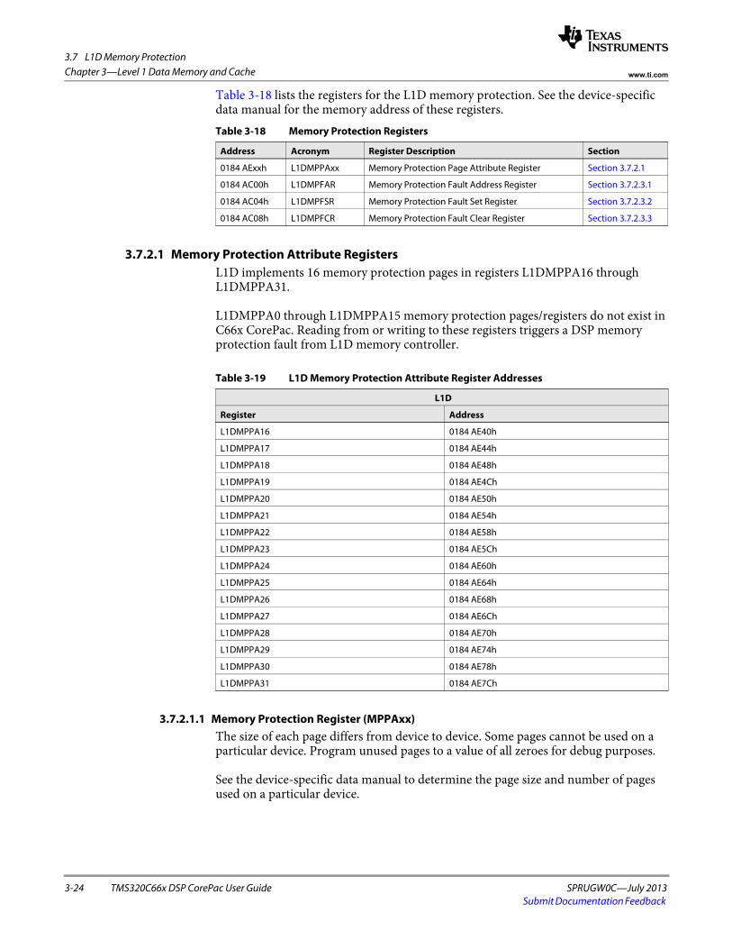
3.7 L1D Memory Protection
3-24 TMS320C66x DSP CorePac User Guide SPRUGW0C—July 2013Submit Documentation Feedback
Chapter 3—Level 1 Data Memory and Cache www.ti.com
Table 3-18 lists the registers for the L1D memory protection. See the device-specific data manual for the memory address of these registers.
3.7.2.1 Memory Protection Attribute RegistersL1D implements 16 memory protection pages in registers L1DMPPA16 through L1DMPPA31.
L1DMPPA0 through L1DMPPA15 memory protection pages/registers do not exist in C66x CorePac. Reading from or writing to these registers triggers a DSP memory protection fault from L1D memory controller.
3.7.2.1.1 Memory Protection Register (MPPAxx)The size of each page differs from device to device. Some pages cannot be used on a particular device. Program unused pages to a value of all zeroes for debug purposes.
See the device-specific data manual to determine the page size and number of pages used on a particular device.
Table 3-18 Memory Protection Registers
Address Acronym Register Description Section
0184 AExxh L1DMPPAxx Memory Protection Page Attribute Register Section 3.7.2.1
0184 AC00h L1DMPFAR Memory Protection Fault Address Register Section 3.7.2.3.1
0184 AC04h L1DMPFSR Memory Protection Fault Set Register Section 3.7.2.3.2
0184 AC08h L1DMPFCR Memory Protection Fault Clear Register Section 3.7.2.3.3
Table 3-19 L1D Memory Protection Attribute Register Addresses
L1D
Register Address
L1DMPPA16 0184 AE40h
L1DMPPA17 0184 AE44h
L1DMPPA18 0184 AE48h
L1DMPPA19 0184 AE4Ch
L1DMPPA20 0184 AE50h
L1DMPPA21 0184 AE54h
L1DMPPA22 0184 AE58h
L1DMPPA23 0184 AE5Ch
L1DMPPA24 0184 AE60h
L1DMPPA25 0184 AE64h
L1DMPPA26 0184 AE68h
L1DMPPA27 0184 AE6Ch
L1DMPPA28 0184 AE70h
L1DMPPA29 0184 AE74h
L1DMPPA30 0184 AE78h
L1DMPPA31 0184 AE7Ch
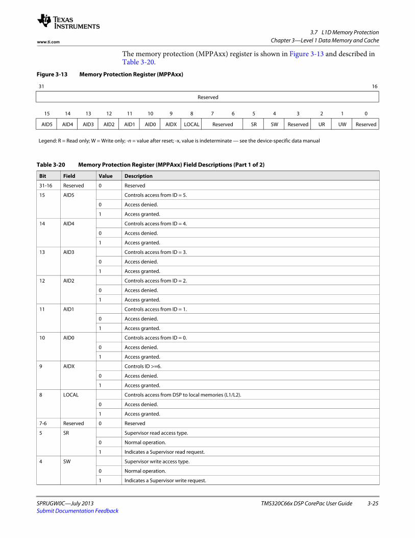
3.7 L1D Memory Protection
SPRUGW0C—July 2013 TMS320C66x DSP CorePac User Guide 3-25Submit Documentation Feedback
Chapter 3—Level 1 Data Memory and Cachewww.ti.com
The memory protection (MPPAxx) register is shown in Figure 3-13 and described in Table 3-20.
Figure 3-13 Memory Protection Register (MPPAxx)
31 16
Reserved
15 14 13 12 11 10 9 8 7 6 5 4 3 2 1 0
AID5 AID4 AID3 AID2 AID1 AID0 AIDX LOCAL Reserved SR SW Reserved UR UW Reserved
Legend: R = Read only; W = Write only; -n = value after reset; -x, value is indeterminate — see the device-specific data manual
Table 3-20 Memory Protection Register (MPPAxx) Field Descriptions (Part 1 of 2)
Bit Field Value Description
31-16 Reserved 0 Reserved
15 AID5 Controls access from ID = 5.
0 Access denied.
1 Access granted.
14 AID4 Controls access from ID = 4.
0 Access denied.
1 Access granted.
13 AID3 Controls access from ID = 3.
0 Access denied.
1 Access granted.
12 AID2 Controls access from ID = 2.
0 Access denied.
1 Access granted.
11 AID1 Controls access from ID = 1.
0 Access denied.
1 Access granted.
10 AID0 Controls access from ID = 0.
0 Access denied.
1 Access granted.
9 AIDX Controls ID >=6.
0 Access denied.
1 Access granted.
8 LOCAL Controls access from DSP to local memories (L1/L2).
0 Access denied.
1 Access granted.
7-6 Reserved 0 Reserved
5 SR Supervisor read access type.
0 Normal operation.
1 Indicates a Supervisor read request.
4 SW Supervisor write access type.
0 Normal operation.
1 Indicates a Supervisor write request.
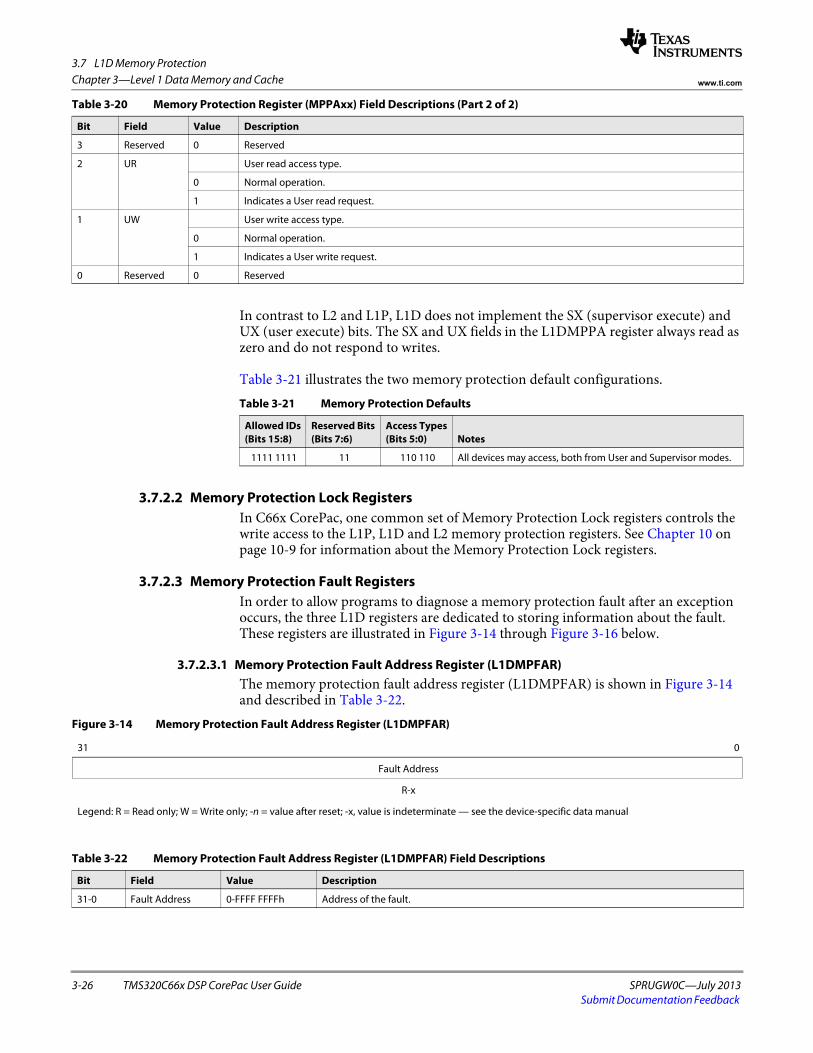
3.7 L1D Memory Protection
3-26 TMS320C66x DSP CorePac User Guide SPRUGW0C—July 2013Submit Documentation Feedback
Chapter 3—Level 1 Data Memory and Cache www.ti.com
In contrast to L2 and L1P, L1D does not implement the SX (supervisor execute) and UX (user execute) bits. The SX and UX fields in the L1DMPPA register always read as zero and do not respond to writes.
Table 3-21 illustrates the two memory protection default configurations.
3.7.2.2 Memory Protection Lock RegistersIn C66x CorePac, one common set of Memory Protection Lock registers controls the write access to the L1P, L1D and L2 memory protection registers. See Chapter 10 on page 10-9 for information about the Memory Protection Lock registers.
3.7.2.3 Memory Protection Fault RegistersIn order to allow programs to diagnose a memory protection fault after an exception occurs, the three L1D registers are dedicated to storing information about the fault. These registers are illustrated in Figure 3-14 through Figure 3-16 below.
3.7.2.3.1 Memory Protection Fault Address Register (L1DMPFAR) The memory protection fault address register (L1DMPFAR) is shown in Figure 3-14 and described in Table 3-22.
3 Reserved 0 Reserved
2 UR User read access type.
0 Normal operation.
1 Indicates a User read request.
1 UW User write access type.
0 Normal operation.
1 Indicates a User write request.
0 Reserved 0 Reserved
Table 3-20 Memory Protection Register (MPPAxx) Field Descriptions (Part 2 of 2)
Bit Field Value Description
Table 3-21 Memory Protection Defaults
Allowed IDs (Bits 15:8)
Reserved Bits (Bits 7:6)
Access Types (Bits 5:0) Notes
1111 1111 11 110 110 All devices may access, both from User and Supervisor modes.
Figure 3-14 Memory Protection Fault Address Register (L1DMPFAR)
31 0
Fault Address
R-x
Legend: R = Read only; W = Write only; -n = value after reset; -x, value is indeterminate — see the device-specific data manual
Table 3-22 Memory Protection Fault Address Register (L1DMPFAR) Field Descriptions
Bit Field Value Description
31-0 Fault Address 0-FFFF FFFFh Address of the fault.
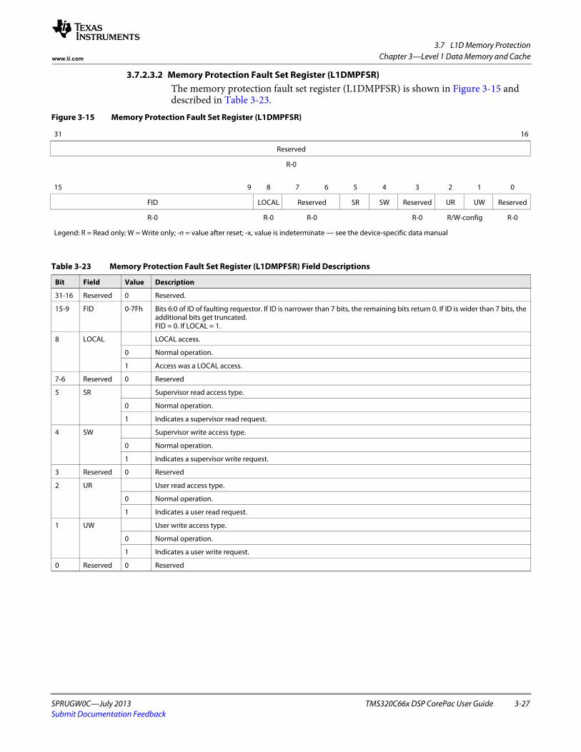
3.7 L1D Memory Protection
SPRUGW0C—July 2013 TMS320C66x DSP CorePac User Guide 3-27Submit Documentation Feedback
Chapter 3—Level 1 Data Memory and Cachewww.ti.com
3.7.2.3.2 Memory Protection Fault Set Register (L1DMPFSR)The memory protection fault set register (L1DMPFSR) is shown in Figure 3-15 and described in Table 3-23.
Figure 3-15 Memory Protection Fault Set Register (L1DMPFSR)
31 16
Reserved
R-0
15 9 8 7 6 5 4 3 2 1 0
FID LOCAL Reserved SR SW Reserved UR UW Reserved
R-0 R-0 R-0 R-0 R/W-config R-0
Legend: R = Read only; W = Write only; -n = value after reset; -x, value is indeterminate — see the device-specific data manual
Table 3-23 Memory Protection Fault Set Register (L1DMPFSR) Field Descriptions
Bit Field Value Description
31-16 Reserved 0 Reserved.
15-9 FID 0-7Fh Bits 6:0 of ID of faulting requestor. If ID is narrower than 7 bits, the remaining bits return 0. If ID is wider than 7 bits, the additional bits get truncated. FID = 0. If LOCAL = 1.
8 LOCAL LOCAL access.
0 Normal operation.
1 Access was a LOCAL access.
7-6 Reserved 0 Reserved
5 SR Supervisor read access type.
0 Normal operation.
1 Indicates a supervisor read request.
4 SW Supervisor write access type.
0 Normal operation.
1 Indicates a supervisor write request.
3 Reserved 0 Reserved
2 UR User read access type.
0 Normal operation.
1 Indicates a user read request.
1 UW User write access type.
0 Normal operation.
1 Indicates a user write request.
0 Reserved 0 Reserved

3.7 L1D Memory Protection
3-28 TMS320C66x DSP CorePac User Guide SPRUGW0C—July 2013Submit Documentation Feedback
Chapter 3—Level 1 Data Memory and Cache www.ti.com
3.7.2.3.3 Memory Protection Fault Clear Register (L1DMPFCR)The memory protection fault clear register (L1DMPFCR) is shown in Figure 3-16 and described in Table 3-24.
Chapter 10 on page 10-1 provides the definition and meanings for these registers.
The L1DMPFAR and L1DMPFSR registers only store enough information for one fault. The hardware records the information about the first fault and generates an exception only for that fault.
The fault information is preserved until software clears it by writing a 1 to the MPFCLR field in the L1DMPFCR register. Writing a 0 to the MPFCLR field in the L1DMPFCR has no effect. L1D ignores the value written to bits 31:1 of the L1DMPFCR register.
3.7.3 Protection Checks on Accesses to Memory Protection RegistersL1D implements permission checks on the memory protection registers themselves. The rules are as follows:
• All requestors may read any L1D memory protection (L1DMP) register at any time in all circumstances.
• Supervisor may write the registers.
Table 3-25 summarizes which L1D memory protection registers are accessible and what protection checks are performed in the C66x CorePac according to role.
Figure 3-16 Memory Protection Fault Clear Register (L1DMPFCR)
31 16
Reserved
R-0
15 0
MPFCLR
W-0
Legend: R = Read only; W = Write only; -n = value after reset; -x, value is indeterminate — see the device-specific data manual
Table 3-24 Memory Protection Fault Clear Register (L1DMPFCR) Field Descriptions
Bit Field Value Description
31-1 Reserved 0 Reserved.
0 MPFCLR Command to clear the L1DMPFAR register.
0 No effect.
1 Clear the L1DMPFAR and the L1DMPFCR registers.
Table 3-25 Permissions for L1D Memory Protection Registers
Register Supervisor User
L1DMPFAR R R
L1DMPFSR R R
L1DMPFCR W /
L1DMPPAxx R/W R

SPRUGW0C—July 2013 TMS320C66x DSP CorePac User Guide 4-1Submit Documentation Feedback
Chapter 4
Level 2 Memory and Cache
4.1 "Introduction" on page 4-2 4.2 "Level 2 Memory Architecture" on page 4-3 4.3 "L2 Cache" on page 4-4 4.4 "L2 Cache Control Registers" on page 4-14 4.5 "L2 Power-Down" on page 4-28 4.6 "L2 Memory Protection" on page 4-29 4.7 "MDMA Bus Error Reporting" on page 4-36

4.1 Introduction
4-2 TMS320C66x DSP CorePac User Guide SPRUGW0C—July 2013Submit Documentation Feedback
Chapter 4—Level 2 Memory and Cache www.ti.com
4.1 Introduction4.1.1 Purpose of the Level 2 (L2) Memory and Cache
The L2 memory controller provides an on-chip memory solution between the faster level 1 memories (L1D, L1P) and slower external memories. It is advantageous in that it supports larger memory sizes than the L1 memories, while providing faster access than external memories.
Similar to the L1 memories, you can configure L2 to provide both cached and non-cached (i.e., addressable) memories.
4.1.2 FeaturesThe L2 memory and cache provides the memory flexibility required in a device using the C66x CorePac:
• Configurable L2 cache size: 32KB, 64KB, 128KB, 256KB, 512KB or 1MB• Memory protection • Supports cache block and global coherence operations
4.1.3 Terms and DefinitionsSee Appendix A on page A-1 and Appendix B on page B-1 of this document for detailed definitions of the terms used in this chapter. Appendix A on page A-1 describes general terms used throughout this reference guide. Appendix B on page B-1 defines terms related to the memory and cache architecture.
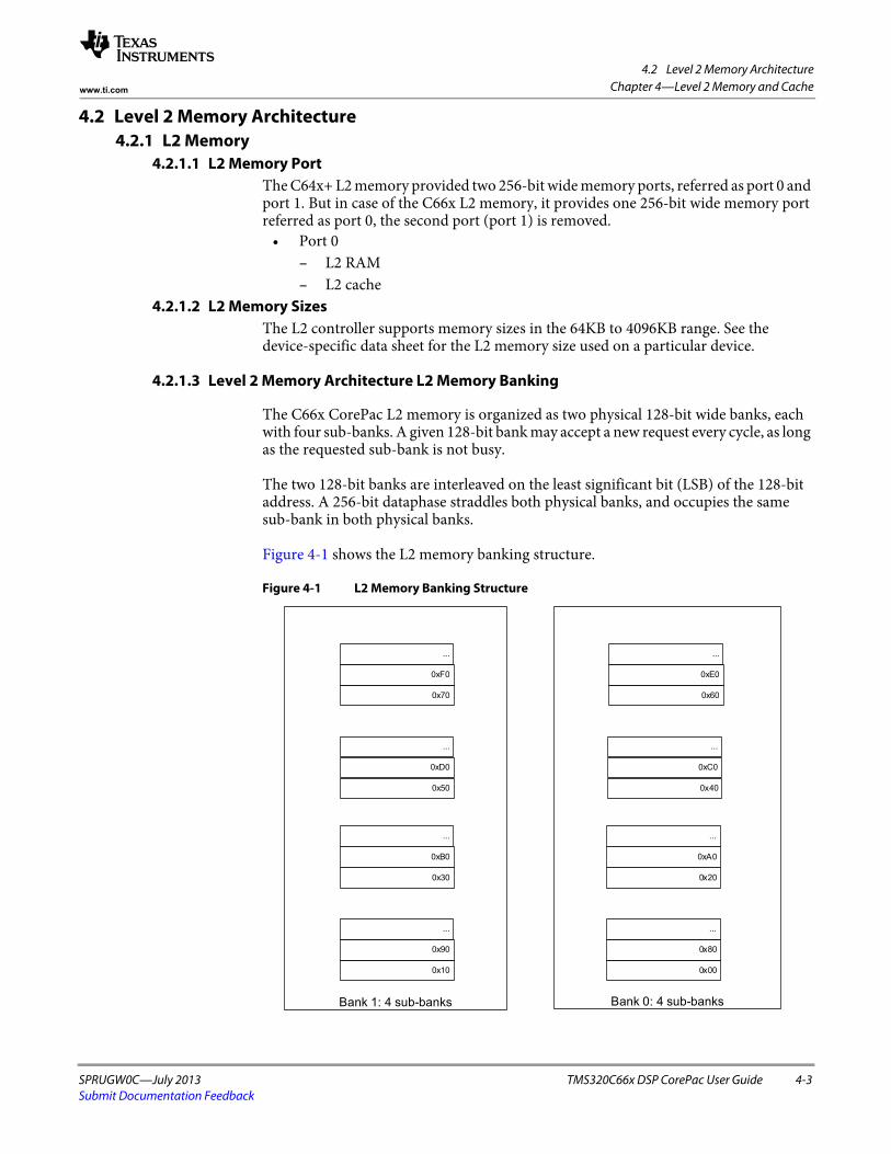
4.2 Level 2 Memory Architecture
SPRUGW0C—July 2013 TMS320C66x DSP CorePac User Guide 4-3Submit Documentation Feedback
Chapter 4—Level 2 Memory and Cachewww.ti.com
4.2 Level 2 Memory Architecture4.2.1 L2 Memory
4.2.1.1 L2 Memory PortThe C64x+ L2 memory provided two 256-bit wide memory ports, referred as port 0 and port 1. But in case of the C66x L2 memory, it provides one 256-bit wide memory port referred as port 0, the second port (port 1) is removed.
• Port 0– L2 RAM– L2 cache
4.2.1.2 L2 Memory Sizes The L2 controller supports memory sizes in the 64KB to 4096KB range. See the device-specific data sheet for the L2 memory size used on a particular device.
4.2.1.3 Level 2 Memory Architecture L2 Memory Banking
The C66x CorePac L2 memory is organized as two physical 128-bit wide banks, each with four sub-banks. A given 128-bit bank may accept a new request every cycle, as long as the requested sub-bank is not busy.
The two 128-bit banks are interleaved on the least significant bit (LSB) of the 128-bit address. A 256-bit dataphase straddles both physical banks, and occupies the same sub-bank in both physical banks.
Figure 4-1 shows the L2 memory banking structure.
Figure 4-1 L2 Memory Banking Structure
Bank 1: 4 sub-banks Bank 0: 4 sub-banks
0x20
0xA0
...
0x40
0xC0
...
0x60
0xE0
...
0x10
0x90
...
0x30
0xB0
...
0x50
0xD0
...
0x70
0xF0
...
0x00
0x80
...
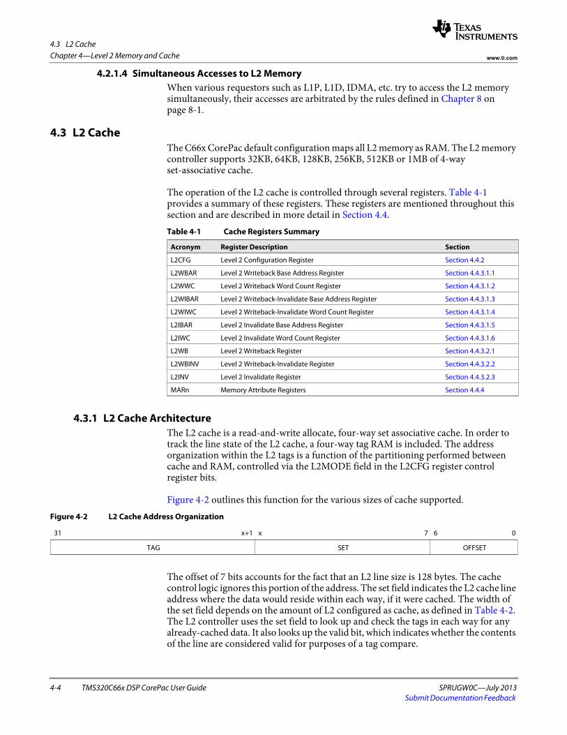
4.3 L2 Cache
4-4 TMS320C66x DSP CorePac User Guide SPRUGW0C—July 2013Submit Documentation Feedback
Chapter 4—Level 2 Memory and Cache www.ti.com
4.2.1.4 Simultaneous Accesses to L2 Memory When various requestors such as L1P, L1D, IDMA, etc. try to access the L2 memory simultaneously, their accesses are arbitrated by the rules defined in Chapter 8 on page 8-1.
4.3 L2 CacheThe C66x CorePac default configuration maps all L2 memory as RAM. The L2 memory controller supports 32KB, 64KB, 128KB, 256KB, 512KB or 1MB of 4-way set-associative cache.
The operation of the L2 cache is controlled through several registers. Table 4-1 provides a summary of these registers. These registers are mentioned throughout this section and are described in more detail in Section 4.4.
4.3.1 L2 Cache Architecture The L2 cache is a read-and-write allocate, four-way set associative cache. In order to track the line state of the L2 cache, a four-way tag RAM is included. The address organization within the L2 tags is a function of the partitioning performed between cache and RAM, controlled via the L2MODE field in the L2CFG register control register bits.
Figure 4-2 outlines this function for the various sizes of cache supported.
The offset of 7 bits accounts for the fact that an L2 line size is 128 bytes. The cache control logic ignores this portion of the address. The set field indicates the L2 cache line address where the data would reside within each way, if it were cached. The width of the set field depends on the amount of L2 configured as cache, as defined in Table 4-2. The L2 controller uses the set field to look up and check the tags in each way for any already-cached data. It also looks up the valid bit, which indicates whether the contents of the line are considered valid for purposes of a tag compare.
Table 4-1 Cache Registers Summary
Acronym Register Description Section
L2CFG Level 2 Configuration Register Section 4.4.2
L2WBAR Level 2 Writeback Base Address Register Section 4.4.3.1.1
L2WWC Level 2 Writeback Word Count Register Section 4.4.3.1.2
L2WIBAR Level 2 Writeback-Invalidate Base Address Register Section 4.4.3.1.3
L2WIWC Level 2 Writeback-Invalidate Word Count Register Section 4.4.3.1.4
L2IBAR Level 2 Invalidate Base Address Register Section 4.4.3.1.5
L2IWC Level 2 Invalidate Word Count Register Section 4.4.3.1.6
L2WB Level 2 Writeback Register Section 4.4.3.2.1
L2WBINV Level 2 Writeback-Invalidate Register Section 4.4.3.2.2
L2INV Level 2 Invalidate Register Section 4.4.3.2.3
MARn Memory Attribute Registers Section 4.4.4
Figure 4-2 L2 Cache Address Organization
31 x+1 x 7 6 0
TAG SET OFFSET
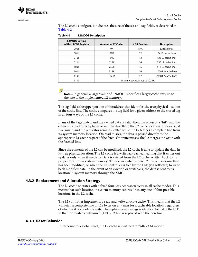
4.3 L2 Cache
SPRUGW0C—July 2013 TMS320C66x DSP CorePac User Guide 4-5Submit Documentation Feedback
Chapter 4—Level 2 Memory and Cachewww.ti.com
The L2 cache configuration dictates the size of the set and tag fields, as described in Table 4-2.
Note—In general, a larger value of L2MODE specifies a larger cache size, up to the size of the implemented L2 memory.
The tag field is the upper portion of the address that identifies the true physical location of the cache line. The cache compares the tag field for a given address to the stored tag in all four ways of the L2 cache.
If any of the tags match and the cached data is valid, then the access is a “hit”, and the element is read directly from or written directly to the L2 cache location. Otherwise, it is a “miss”, and the requestor remains stalled while the L2 fetches a complete line from its system memory location. On read misses, the data is passed directly to the appropriate L1 cache as part of the fetch. On write misses, the L2 merges the write with the fetched line.
Since the contents of the L2 can be modified, the L2 cache is able to update the data in its true physical location. The L2 cache is a writeback cache, meaning that it writes out updates only when it needs to. Data is evicted from the L2 cache, written back to its proper location in system memory. This occurs when a new L2 line replaces one that has been modified, or when the L2 controller is told by the DSP (via software) to write back modified data. In the event of an eviction or writeback, the data is sent to its location in system memory through the XMC.
4.3.2 Replacement and Allocation Strategy The L2 cache operates with a fixed four-way set associativity in all cache modes. This means that each location in system memory can reside in any one of four possible locations in the L2 cache.
The L2 controller implements a read and write-allocate cache. This means that the L2 will fetch a complete line of 128 bytes on any miss for a cacheable location, regardless of whether it is a read or a write. The replacement strategy is identical to that of the L1D, in that the least-recently-used (LRU) L2 line is replaced with the new line.
4.3.3 Reset BehaviorIn response to a global reset, the L2 cache is switched to “All-RAM mode.”
Table 4-2 L2MODE Description
L2MODE Setting of the L2CFG Register Amount of L2 Cache X Bit Position Description
000b 0K N/A L2 is all RAM
001b 32K 12 64 L2 cache lines
010b 64K 13 128 L2 cache lines
011b 128K 14 256 L2 cache lines
100b 256K 15 512 L2 cache lines
101b 512K 16 1024 L2 cache lines
110b 1024K 17 2048 L2 cache lines
111b Maximal cache. Maps to 1024K.
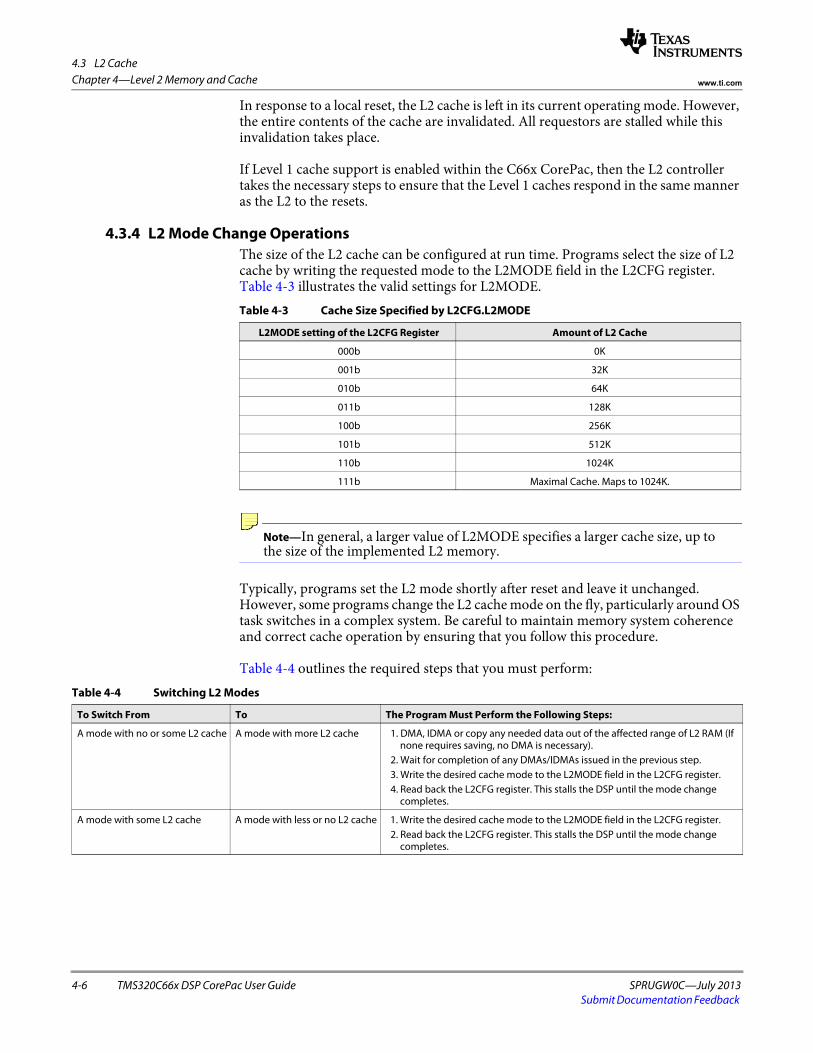
4.3 L2 Cache
4-6 TMS320C66x DSP CorePac User Guide SPRUGW0C—July 2013Submit Documentation Feedback
Chapter 4—Level 2 Memory and Cache www.ti.com
In response to a local reset, the L2 cache is left in its current operating mode. However, the entire contents of the cache are invalidated. All requestors are stalled while this invalidation takes place.
If Level 1 cache support is enabled within the C66x CorePac, then the L2 controller takes the necessary steps to ensure that the Level 1 caches respond in the same manner as the L2 to the resets.
4.3.4 L2 Mode Change OperationsThe size of the L2 cache can be configured at run time. Programs select the size of L2 cache by writing the requested mode to the L2MODE field in the L2CFG register. Table 4-3 illustrates the valid settings for L2MODE.
Note—In general, a larger value of L2MODE specifies a larger cache size, up to the size of the implemented L2 memory.
Typically, programs set the L2 mode shortly after reset and leave it unchanged. However, some programs change the L2 cache mode on the fly, particularly around OS task switches in a complex system. Be careful to maintain memory system coherence and correct cache operation by ensuring that you follow this procedure.
Table 4-4 outlines the required steps that you must perform:
Table 4-3 Cache Size Specified by L2CFG.L2MODE
L2MODE setting of the L2CFG Register Amount of L2 Cache
000b 0K
001b 32K
010b 64K
011b 128K
100b 256K
101b 512K
110b 1024K
111b Maximal Cache. Maps to 1024K.
Table 4-4 Switching L2 Modes
To Switch From To The Program Must Perform the Following Steps:
A mode with no or some L2 cache A mode with more L2 cache 1. DMA, IDMA or copy any needed data out of the affected range of L2 RAM (If none requires saving, no DMA is necessary).
2. Wait for completion of any DMAs/IDMAs issued in the previous step.3. Write the desired cache mode to the L2MODE field in the L2CFG register.4. Read back the L2CFG register. This stalls the DSP until the mode change
completes.
A mode with some L2 cache A mode with less or no L2 cache 1. Write the desired cache mode to the L2MODE field in the L2CFG register.2. Read back the L2CFG register. This stalls the DSP until the mode change
completes.

4.3 L2 Cache
SPRUGW0C—July 2013 TMS320C66x DSP CorePac User Guide 4-7Submit Documentation Feedback
Chapter 4—Level 2 Memory and Cachewww.ti.com
When a program writes a new cache mode to the L2CFG register, the L2 performs the following steps:
• L2 cache is written back and invalidated if it is enabled. • The L2 cache sets to the requested mode.
Note—Changing L2's mode does not affect the contents of either L1 cache.
4.3.5 L2 Freeze ModeThe L2 cache offers a freeze mode. The content of the L2 cache is frozen in this mode (i.e., it will not update as during normal operation). L2 freeze mode allows real-time applications to limit the amount of data evicted from L2 during various sections of code, such as interrupt handlers. Use the L2CC field in the L2CFG register to set this mode.
The freeze mode affects the operation of L2 cache only. L2 RAM is not affected by this mode. L2’s freeze mode has no impact on L1D or L1P caches. Likewise, the L1's freeze modes have no impact on L2 cache.
The L2 cache responds to read and write hits normally when in freeze mode. L2 sends read and write misses directly to external memory, as if L2 cache were not present. The L2 never allocates a new cache line while frozen. Lines may only be evicted from L2 during freeze mode by program-initiated cache coherence operations, as defined in Section 4.3.6.
Table 4-5 provides a summary of the L2 freeze mode, set through the L2CC field in the L2CFG register.
4.3.6 Program Initiated Cache Coherence OperationsThe L2 memory architecture supports a variety of coherence operations that fall into two primary categories: block operations that operate on a specific range of addresses, and global operations which operate on the entire contents of one or more caches.
The following cache coherence operations are supported: • Invalidation: Valid cache lines are made invalid. Content of the affected cache
lines is discarded • Writeback: The content of a valid and dirty cache line is written to a lower-level
memory.• Writeback-invalidation: Writeback operation followed by invalidation. Only the
content of the affected cache lines is written to lower-level memory, but all the lines are invalidated.
Table 4-5 Freeze Mode Summary
L2 Mode L2MODE L2 CacheEnabled L2CC = 0
L2 Cache EnabledL2CC = 0
L2 Cache FreezeL2CC = 1
All RAM 000 No effect, because L2 is all RAM.
Mixed cache and RAMor all cache.
1000 Cache operates normally. Cache frozen. Hits proceed normally. L1D misses are serviced as long-distance accesses for requested bytes only. L1P misses serviced as long-distance fetch for 1 fetch packet. No LRU updates in this mode.
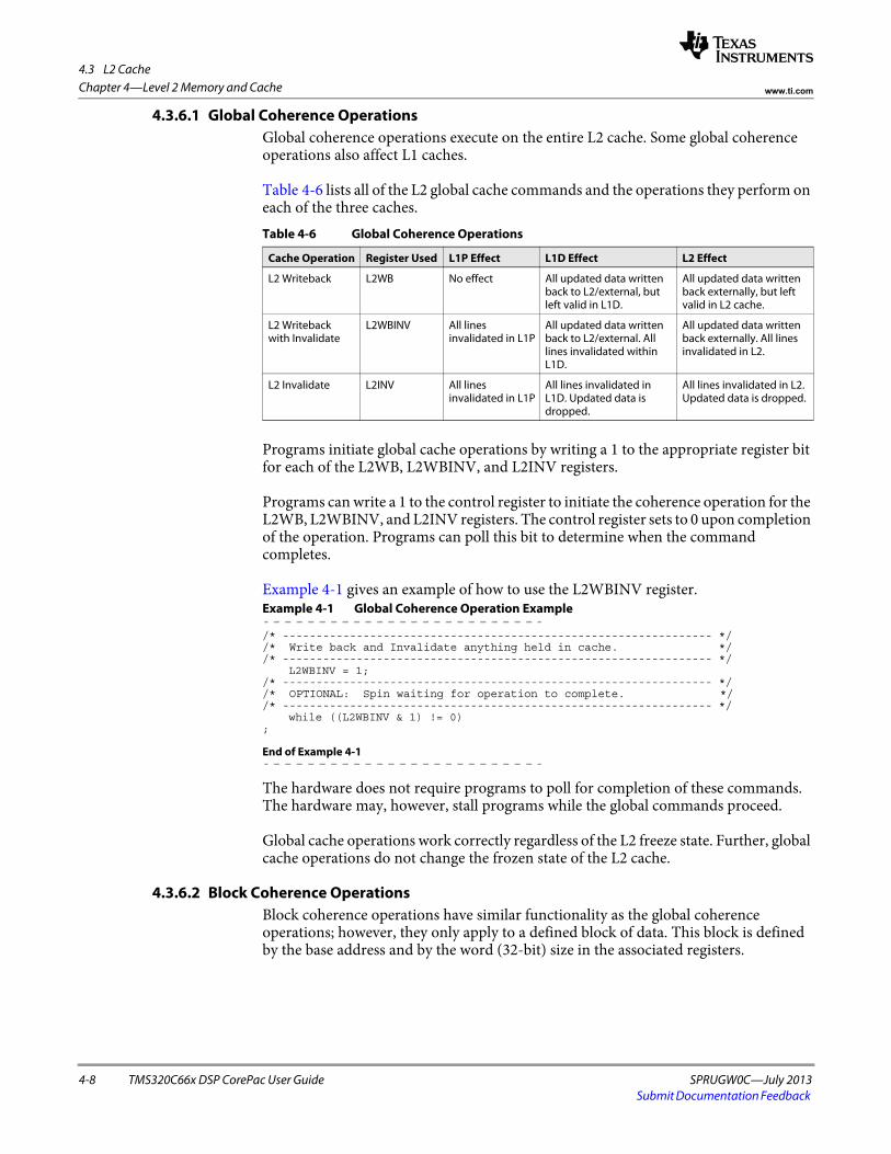
4.3 L2 Cache
4-8 TMS320C66x DSP CorePac User Guide SPRUGW0C—July 2013Submit Documentation Feedback
Chapter 4—Level 2 Memory and Cache www.ti.com
4.3.6.1 Global Coherence Operations Global coherence operations execute on the entire L2 cache. Some global coherence operations also affect L1 caches.
Table 4-6 lists all of the L2 global cache commands and the operations they perform on each of the three caches.
Programs initiate global cache operations by writing a 1 to the appropriate register bit for each of the L2WB, L2WBINV, and L2INV registers.
Programs can write a 1 to the control register to initiate the coherence operation for the L2WB, L2WBINV, and L2INV registers. The control register sets to 0 upon completion of the operation. Programs can poll this bit to determine when the command completes.
Example 4-1 gives an example of how to use the L2WBINV register.Example 4-1 Global Coherence Operation Example
/* ---------------------------------------------------------------- */ /* Write back and Invalidate anything held in cache. *//* ---------------------------------------------------------------- */
L2WBINV = 1; /* ---------------------------------------------------------------- */ /* OPTIONAL: Spin waiting for operation to complete. *//* ---------------------------------------------------------------- */
while ((L2WBINV & 1) != 0) ;
End of Example 4-1
The hardware does not require programs to poll for completion of these commands. The hardware may, however, stall programs while the global commands proceed.
Global cache operations work correctly regardless of the L2 freeze state. Further, global cache operations do not change the frozen state of the L2 cache.
4.3.6.2 Block Coherence OperationsBlock coherence operations have similar functionality as the global coherence operations; however, they only apply to a defined block of data. This block is defined by the base address and by the word (32-bit) size in the associated registers.
Table 4-6 Global Coherence Operations
Cache Operation Register Used L1P Effect L1D Effect L2 Effect
L2 Writeback L2WB No effect All updated data written back to L2/external, but left valid in L1D.
All updated data written back externally, but left valid in L2 cache.
L2 Writeback with Invalidate
L2WBINV All lines invalidated in L1P
All updated data written back to L2/external. All lines invalidated within L1D.
All updated data written back externally. All lines invalidated in L2.
L2 Invalidate L2INV All lines invalidated in L1P
All lines invalidated in L1D. Updated data is dropped.
All lines invalidated in L2. Updated data is dropped.

4.3 L2 Cache
SPRUGW0C—July 2013 TMS320C66x DSP CorePac User Guide 4-9Submit Documentation Feedback
Chapter 4—Level 2 Memory and Cachewww.ti.com
Table 4-7 lists all of the block cache commands and the operation they perform on each of the three caches.
Programs initiate block cache operations by writing a word address to the base address register, and then writing a word count to the word count register. (Writing 1 to WC indicates a length of 4 bytes). If necessary, C66x CorePac enforces one or both of the following:
• Only one program-initiated coherence operation may be in progress at a time.• Writes to either L2XXBAR or L2XXWC stall while another block or global cache
coherence operation is in progress.
The L2XXBAR/L2XXWC mechanism for setting up block cache operations allows you to specify ranges down to word granularity. However, the memory system operates at cache-line granularity. Thus, all cache lines that overlap the range specified are acted upon.
On the C66x DSP, it is recommended that programs wait for block coherence operations to complete before continuing. To issue a block coherence operation:
1. Write the starting address to the L2XXBAR register.2. Write the word count to the L2XXWC register.3. Wait for completion by one of the following methods:
a. Issue an MFENCE instruction (preferred), orb. Poll the L2XXWC register until the word count field reads as zero.
The MFENCE instruction is new to the C66x DSP. It stalls the DSP until all outstanding memory operations complete. For further information about MFENCE instruction, see the C66x DSP and Instruction Set Reference Guide (SPRUGH7) in ‘‘Related Documentation from Texas Instruments’’ on page ø-xx.
Example 4-2 gives the pseudo-code sequence of the block coherence operation.
Example 4-2 Block Coherence Operation Example
/* ---------------------------------------------------------------- *//* Write base address of array to Base Address Register. *//* Then write the length of the array, in words, to the Word *//* Count register. *//* ---------------------------------------------------------------- */
L2WBAR = &array[0];L2WWC = sizeof(array) / sizeof(int);
Table 4-7 Block Cache Operations
Cache Operation Register Used L1P Effect L1D Effect L2 Effect
L2 Writeback L2WBAR
L2WWC
No effect Updated data written back to L2/external, but left valid in L1D
Updated data written back externally, but left valid in L2 cache.
L2 Writeback with Invalidate
L2WIBAR
L2WIWC
All lines in rangeinvalidated in L1P
Updated data written back to L2/external. All lines in range invalidated with L1D.
Updated data written back externally. All lines in range invalidated in L2.
L2 Invalidate L2IBAR
L2IWC
All lines in rangeinvalidated in L1P
All lines in range invalidated in L1D. Updated data is dropped.
All lines in range invalidated in L2. Updated data is dropped.
4.3 L2 Cache
4-10 TMS320C66x DSP CorePac User Guide SPRUGW0C—July 2013Submit Documentation Feedback
Chapter 4—Level 2 Memory and Cache www.ti.com
/* ---------------------------------------------------------------- */ /* Wait for coherence operation to complete. *//* ---------------------------------------------------------------- */
asm (" MFENCE");
End of Example 4-2
Writing to the L2XXBAR register sets up the base address for the next cache coherency operation. Writing a non-zero value to L2XXWC initiates the operation. Programs should not rely on the contents of L2XXBAR after or during a cache control operation; rather, programs should always write a new value to L2XXBAR prior to writing L2XXWC. Reading L2XXWC returns a non-zero value while a block cache operation is in progress, and zero when it is complete. Block cache operations work correctly regardless of the L2 freeze state.
4.3.7 Cacheability ControlsIn some applications, some specific addresses may need to be read from their physical locations each time they are accessed (e.g., a status register within FPGA).
The L2 controller offers registers that control whether certain ranges of memory are cacheable, and whether one or more requestors are actually permitted to access these ranges. The registers are referred to as MARs (memory attribute registers). A complete list of MAR registers is provided in Section 4.4.4.
Note—Using the volatile keyword in the C language does not protect a variable from being cached. If an application uses a memory location periodically updated by external hardware, in order to protect this operation in C code follow these two steps:
• Use the volatile keyword to prevent the code generation tools from incorrectly optimizing the variable.
• You must program the MAR register of the range containing the variable to prevent caching.
4.3.7.1 MAR FunctionsEach MAR register implements two bits - Permit Copies (PC) and Prefetchable Externally (PFX). The PC bit in each MAR register controls whether the cache may hold a copy of the affected address range. If PC = 1, the affected address range is cacheable. If PC = 0, the affected address range is not cacheable. The PFX bit in each MAR register is used to convey to the XMC whether a given address range is prefetchable. If PFX = 1, the affected address range is prefetchable. If PFX = 0, the affected address range is not prefetchable.
4.3.7.2 Special MAR Registers MAR0 through MAR15 represent reserved address ranges in the C66x CorePac, and therefore are treated as follows:
1. MAR0 is implemented as a read-only register. The PC of the MAR0 is always read as 1.
2. MAR1 through MAR11 correspond to internal and external configuration address spaces. Therefore, these registers are read-only, and their PC field reads as 0.
3. MAR12 through MAR15 correspond to MSMC memory. These are read-only registers, the PC always read as 1. This makes the MSMC memory always cacheable within L1D when accessed by its primary address range.
4.3 L2 Cache
SPRUGW0C—July 2013 TMS320C66x DSP CorePac User Guide 4-11Submit Documentation Feedback
Chapter 4—Level 2 Memory and Cachewww.ti.com
Because MAR0 through MAR15 are read-only, the software does not need to manipulate these registers.
4.3.7.3 Requirements for updating MAR registers at runtimeMAR registers are runtime programmable, except as noted in Section 4.3.7.2. All MAR register bits reset to a value of 0, thereby making the entire address space non-cacheable by default (except as noted in Section 4.3.7.2).
Whenever MAR registers are updated dynamically, programs must follow the following sequence to ensure that all future accesses to the particular address range are not cached in L1 and L2 caches.
1. Ensure that all addresses within the affected range are removed from the L1 and L2 caches. This is accomplished in one of the following ways. Any one of the following operations should be sufficient.
a. If L2 cache is enabled, invoke a global writeback-invalidate using L2WBINV. Wait for the C bit in L2WBINV to read as 0. Alternately, invoke a block writeback-invalidate of the affected range using L2WIBAR/L2WIWC. Wait for L2WIWC to read as 0.
b. If L2 is in all SRAM mode, invoke a block writeback-invalidate of the affected range using L1DWIBAR/L1DWIWC. Wait for L1DWIWC to read as 0.
Note that the block-oriented cache controls can only operate on a 256K-byte address range at a time, so multiple block writeback-invalidate operations may be necessary to remove the entire affected address range from the cache.
2. Clear the PC bit in the appropriate MAR to 0.
4.3.7.4 L1 InteractionWhen L1P or L1D makes a request to L2 for an address that is not held in L2 RAM or L2 cache, the L2 controller queries the corresponding MAR register for that address. If the permit copies (PC) bit in the MAR register is 0, the L2 cache controller treats this as a non-cacheable access and initiates a long-distance access. If the access is a long distance read, the DSP stalls until the read data returns and the L1D will write-back dirty data if present in the LRU cache set that matches the non-cacheable memory address.
Concerning L1D long distance requests, the net result of the PC bit in the MAR is to prevent non-cacheable data from being stored in the L2 and L1D caches. Thus, when PC = 0 in a given MAR register, neither the L1D nor the L2 cache retains a copy of data accessed within the address range covered by that MAR.
The MAR registers have no effect on L1P. If L1P is enabled, it will always cache program fetches regardless of MAR configuration.
4.3.8 L1-L2 Coherence Support This section describes the interaction imposed by the coherence rules between the L2 cache and the L1D and L1P caches.
The C66x CorePac maintains the following coherence model: 1. Coherence between the C66x CorePac's L2 RAM segments and L1D cache is
maintained.

4.3 L2 Cache
4-12 TMS320C66x DSP CorePac User Guide SPRUGW0C—July 2013Submit Documentation Feedback
Chapter 4—Level 2 Memory and Cache www.ti.com
2. Coherence between the C66x CorePac's L2 RAM segments and L1P cache is not maintained.
3. Coherence between the external memory and cached copies in L1 or L2 caches is not maintained.
The following sections outline the functions that provide the L2-RAM-to-L1cache coherence.
4.3.8.1 Cache Coherence ProtocolIn order to support coherence between the L1 and L2 caches, snoop-read and snoop-write commands are used.
The cache coherence protocol implements some features which are different from the ones implemented in the C64x devices. In the C64x protocol, coherence is supported between DMAs and L1D in L2, but not between DMAs and L1P. Also, in the C64x memory architecture, L1D cache is kept inclusive within L2, and thus requires snoops in response to L2 cache activity. The C64x+/C66x CorePac removes this inclusiveness, thus limiting snoops to those triggered by DMA activity. L1 and L2 are still coherent with respect to each other, even though L1 is not inclusive within L2.
Cache A is inclusive in cache B, if A's contents are always a subset of B's. If a line is held in A, but not in B, then A is not inclusive in B. A non-cacheable write may hit in L2 if the address was previously cacheable. This can happen if applications dynamically change the settings of the MAR registers.
Table 4-8 lists the coherence commands L2 can issue to L1D on a per-cache-line basis.
Note—These snoop commands represent hardware activity that is transparent. They are included to help you understand the cache operation better.
4.3.8.2 L2 Cache Evictions In the C64x memory architecture, when L2 evicts a line, it snoop-invalidates L1D, thereby keeping L1D inclusive in L2. In the C64x+/C66x architecture, when L2 evicts a line, it writes the victim out if it is dirty, without consulting L1D. It does not invalidate the line in L1D. L2 also does not invalidate lines in L1P when evicting a line. As a result, neither L1D nor L1P is inclusive in L2.
4.3.8.3 Policy Relative to L1D Victims L1D victim writebacks do not trigger line allocations in L2. L1D victims are written directly to external memory if they miss L2.
Table 4-8 L2 to L1D Coherence Commands
Snoop Command Name L1D Action Triggered by
SNPR Snoop Read L1D sends L2 the contents of the requested half-line in L1D. Does not modify the dirty/valid/LRU state for the line.
DMA read from L2 RAM when L1D shadow tags say line is present and modified in L1D.
SNPW Snoop Write Up to 256 bits of new data is sent from L2 to L1D. L1D and L2 both update their respective copies of the data. The dirty and valid bits for the line in L1D do not change.
DMA write to L2 RAM when L1D shadow tags say line is present in L1D. Whether the line is modified in L1D does not matter.
4.3 L2 Cache
SPRUGW0C—July 2013 TMS320C66x DSP CorePac User Guide 4-13Submit Documentation Feedback
Chapter 4—Level 2 Memory and Cachewww.ti.com
L1D victim writebacks also do not update L2’s LRU if they hit in L2. They do update L2’s dirty status as needed.
4.3.8.4 DMA/IDMA Write Interaction When a DMA or IDMA write occurs to L2 RAM, the behavior of L2 depends on whether the data is cached in L1D. The behavior in the C64x+/C66x architecture is different from the behavior in the C64x architecture. In the C64x architecture, snoop-invalidate commands are sent to L1P and L1D. In the C64x+/C66x architecture, DMA/IDMA writes never invalidate lines in L1P. DMA/IDMA writes send snoop-writes to L1D if the address range is present in L1D and otherwise nothing.
4.3.8.5 DMA/IDMA Read InteractionThe L2 memory keeps a shadow copy of L1D tags. This shadow includes both 'dirty' and 'valid' status.
When DMA/IDMA read L2 RAM, the L2 consults the shadow tag. If the given address is marked as 'valid' and 'dirty' in L1D, the L2 sends a snoop-read request for the address to L1D. L1D responds with the requested data.
The snoop-read leaves the data valid in L1D, and does not evict or write back the data to L2. As a consequence, a buffer allocated in L1D is to left allocated in L1D so that algorithms running on the DSP can subsequently refill the buffer without incurring cache miss penalties.

4.4 L2 Cache Control Registers
4-14 TMS320C66x DSP CorePac User Guide SPRUGW0C—July 2013Submit Documentation Feedback
Chapter 4—Level 2 Memory and Cache www.ti.com
4.4 L2 Cache Control RegistersThe C66x memory system provides a set of registers to govern the operation of L2 cache. These registers fall into several categories covered in the following sections:
• Cache Size and Operating Mode Controls. These registers control the size of the cache, and whether the cache is frozen or operating normally. They are described in Section 4.4.2.
• Block-oriented and Global Coherence Operations. These operations allow programs to manually move data out of the cache.
• Cacheability Controls. These registers control whether the cache is permitted to store copies of certain ranges of memory. They are described in Section 4.4.4.
4.4.1 Memory Mapped L2 Cache Control Registers OverviewTable 4-9 below lists the L2 cache registers.
4.4.2 L2 Configuration Register (L2CFG)The L2CFG register controls operating the L2 cache. The L2CFG sets the amount of L2 memory that acts as cache, controls L2 freeze modes, and holds L1D/L1P invalidate bits.
The L2 configuration register (L2CFG) is shown in Figure 4-3 and described in Table 4-10.
Table 4-9 Cache Control Registers
Address Acronym Register Description Section
0184 0000h L2CFG L2 Configuration Register Section 4.4.2
0184 4000h L2WBAR L2 Writeback Base Address Register Section 4.4.3.1.1
0184 4004h L2WWC L2 Writeback Word Count Register Section 4.4.3.1.2
0184 4010h L2WIBAR L2 Writeback-Invalidate Base Address Register Section 4.4.3.1.3
0184 4014h L2WIWC L2 Writeback-Invalidate Word Count Register Section 4.4.3.1.4
0184 4018h L2IBAR L2 Invalidate Base Address Register Section 4.4.3.1.5
0184 401Ch L2IWC L2 Invalidate Word Count Register Section 4.4.3.1.6
0184 5000h L2WB L2 Writeback Register Section 4.4.3.2.1
0184 5004h L2WBINV L2 Writeback-Invalidate Register Section 4.4.3.2.2
0184 5008h L2INV L2 Invalidate Register Section 4.4.3.2.3
Figure 4-3 L2 Configuration Register (L2CFG)
31 28 27 24 23 20 19 16
Reserved NUM MM Reserved MMID
R-0 R-config R-0 R-config
15 10 9 8 7 4 3 2 0
Reserved IP ID Reserved L2CC L2MODE
R-0 W-0 W-0 R-0 R/W-0 R/W-0
Legend: R = Read only; W = Write only; -n = value after reset; -x, value is indeterminate — see the device-specific data manual

4.4 L2 Cache Control Registers
SPRUGW0C—July 2013 TMS320C66x DSP CorePac User Guide 4-15Submit Documentation Feedback
Chapter 4—Level 2 Memory and Cachewww.ti.com
4.4.3 L2 Cache Coherence Operation Registers4.4.3.1 Block Coherence Operation Registers
4.4.3.1.1 L2 Writeback Base Address Register (L2WBAR)The L2 writeback base address register (L2WBAR) is shown in Figure 4-4 and described in Table 4-11.
Table 4-10 L2 Configuration Register (L2CFG) Field Descriptions
Bit Field Value Description
31-28 Reserved 0 Reserved
27-24 NUM MM 0-Fh Number of C66x CorePacs minus 1. Used in multi-processing environment.
23-20 Reserved 0 Reserved
19-16 MMID 0-Fh Contains the C66x CorePac ID number. Used in a multiprocessing environment where several C66x CorePacs are present.
15-10 Reserved 0 Reserved
9 IP L1P global invalidate bit. Provided for backward compatibility, C64x+/C66x devices should use the L1PINV register described in Chapter 2 on page 2-1.
0 Normal L1P operation.
1 All L1P lines are invalidated.
8 ID L1D global invalidate bit. Provided for backward compatibility, C64x+/C66x devices should use the L1DINV register described in Chapter 3 on page 3-1.
0 Normal L1D operation.
1 All L1D lines are invalidated.
7-4 Reserved 0 Reserved
3 L2CC Controls the freeze mode
0 Normal operation
1 L2 cache frozen
2-0 L2MODE 0-7h Defines the size of L2 cache.
0h L2 cache disabled.
1h 32K
2h 64K
3h 128K
4h 256K
5h 512K
6h 1024K
7h Maximum cache
Figure 4-4 L2 Writeback Base Address Register (L2WBAR)
31 0
L2 Writeback Base Address (L2WBAR)
W-x
Legend: R = Read only; W = Write only; -n = value after reset; -x, value is indeterminate — see the device-specific data manual
Table 4-11 L2 Writeback Base Address Register (L2WBAR) Field Descriptions
Bit Field Value Description
31-0 L2WBAR 0-FFFF FFFFh Defines the base address for the L2 block writeback operation.
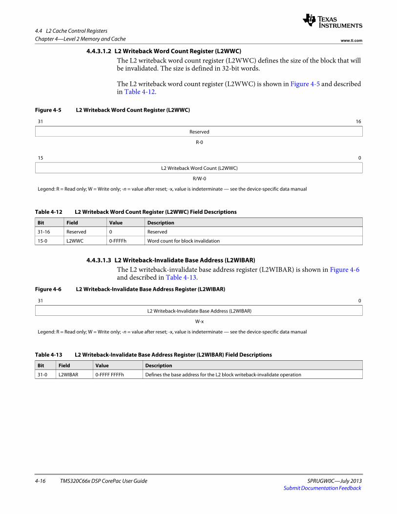
4.4 L2 Cache Control Registers
4-16 TMS320C66x DSP CorePac User Guide SPRUGW0C—July 2013Submit Documentation Feedback
Chapter 4—Level 2 Memory and Cache www.ti.com
4.4.3.1.2 L2 Writeback Word Count Register (L2WWC) The L2 writeback word count register (L2WWC) defines the size of the block that will be invalidated. The size is defined in 32-bit words.
The L2 writeback word count register (L2WWC) is shown in Figure 4-5 and described in Table 4-12.
4.4.3.1.3 L2 Writeback-Invalidate Base Address (L2WIBAR)The L2 writeback-invalidate base address register (L2WIBAR) is shown in Figure 4-6 and described in Table 4-13.
Figure 4-5 L2 Writeback Word Count Register (L2WWC)
31 16
Reserved
R-0
15 0
L2 Writeback Word Count (L2WWC)
R/W-0
Legend: R = Read only; W = Write only; -n = value after reset; -x, value is indeterminate — see the device-specific data manual
Table 4-12 L2 Writeback Word Count Register (L2WWC) Field Descriptions
Bit Field Value Description
31-16 Reserved 0 Reserved
15-0 L2WWC 0-FFFFh Word count for block invalidation
Figure 4-6 L2 Writeback-Invalidate Base Address Register (L2WIBAR)
31 0
L2 Writeback-Invalidate Base Address (L2WIBAR)
W-x
Legend: R = Read only; W = Write only; -n = value after reset; -x, value is indeterminate — see the device-specific data manual
Table 4-13 L2 Writeback-Invalidate Base Address Register (L2WIBAR) Field Descriptions
Bit Field Value Description
31-0 L2WIBAR 0-FFFF FFFFh Defines the base address for the L2 block writeback-invalidate operation

4.4 L2 Cache Control Registers
SPRUGW0C—July 2013 TMS320C66x DSP CorePac User Guide 4-17Submit Documentation Feedback
Chapter 4—Level 2 Memory and Cachewww.ti.com
4.4.3.1.4 L2 Writeback-Invalidate Word Count Register (L2WIWC) The L2 writeback-invalidate word count register (L2WIWC) defines the size of the block that will be invalidated. The size is defined in 32-bit words.
The L2 writeback-invalidate word count register (L2WIWC) is shown in Figure 4-7 and described in Table 4-14.
4.4.3.1.5 L2 Invalidate Base Address Register (L2IBAR)The L2 invalidate base address register (L2IBAR) defines the base address of the block that will be invalidated.
The L2 invalidate base address register (L2IBAR) is shown in Figure 4-8 and described in Table 4-15.
Figure 4-7 L2 Writeback-Invalidate Word Count Register (L2WIWC)
31 16
Reserved
R-0
15 0
L2 Writeback-Invalidate Word Count (L2WIWC)
R/W-0
Legend: R = Read only; W = Write only; -n = value after reset; -x, value is indeterminate — see the device-specific data manual
Table 4-14 L2 Writeback-Invalidate Word Count Register (L2WIWC) Field Descriptions
Bit Field Value Description
31-16 Reserved 0 Reserved
15-0 L2WIWC 0-FFFFh Word count for block invalidation
Figure 4-8 L2 Invalidate Base Address Register (L2IBAR)
31 0
L2 Invalidate Base Address (L2IBAR)
W-x
Legend: R = Read only; W = Write only; -n = value after reset; -x, value is indeterminate — see the device-specific data manual
Table 4-15 L2 Invalidate Base Address Register (L2IBAR) Field Descriptions
Bit Field Value Description
31-0 L2IBAR 0-FFFF FFFFh Defines the base address for the L2 block invalidate operation

4.4 L2 Cache Control Registers
4-18 TMS320C66x DSP CorePac User Guide SPRUGW0C—July 2013Submit Documentation Feedback
Chapter 4—Level 2 Memory and Cache www.ti.com
4.4.3.1.6 L2 Invalidate Word Count Register (L2IWC) The L2 invalidate word count register (L2IWC) defines the size of the block that will be invalidated. The size is defined in 32-bit words.
The L2 invalidate word count register (L2IWC) is shown in Figure 4-9 and described in Table 4-16.
4.4.3.2 Global Coherence Operation Registers4.4.3.2.1 L2 Writeback Register (L2WB)
The L2 writeback register (L2WB) controls the global writeback operation of the L2 cache.
The L2 writeback register (L2WB) is shown in Figure 4-10 and described in Table 4-17.
Figure 4-9 L2 Invalidate Word Count Register (L2IWC)
31 16
Reserved
R-0
15 0
L2 Invalidate Word Count (L2IWC)
R/W-0
Legend: R = Read only; W = Write only; -n = value after reset; -x, value is indeterminate — see the device-specific data manual
Table 4-16 Invalidate Word Count Register (L2IWC) Field Descriptions
Bit Field Value Description
31-16 Reserved 0 Reserved
15-0 L2IWC 0-FFFFh Word count for block invalidation
Figure 4-10 L2 Writeback Register (L2WB)
31 16
Reserved
R-0
15 1 0
Reserved C
R/W-0 R/W-0
Legend: R = Read only; W = Write only; -n = value after reset; -x, value is indeterminate — see the device-specific data manual
Table 4-17 L2 Writeback Register (L2WB) Field Descriptions
Bit Field Value Description
31-1 Reserved 0 Reserved
0 C Controls the global writeback operation of L2 cache as described in Section 4.3.6.1.
0 Normal operation
1 Dirty L2 cache lines are written back
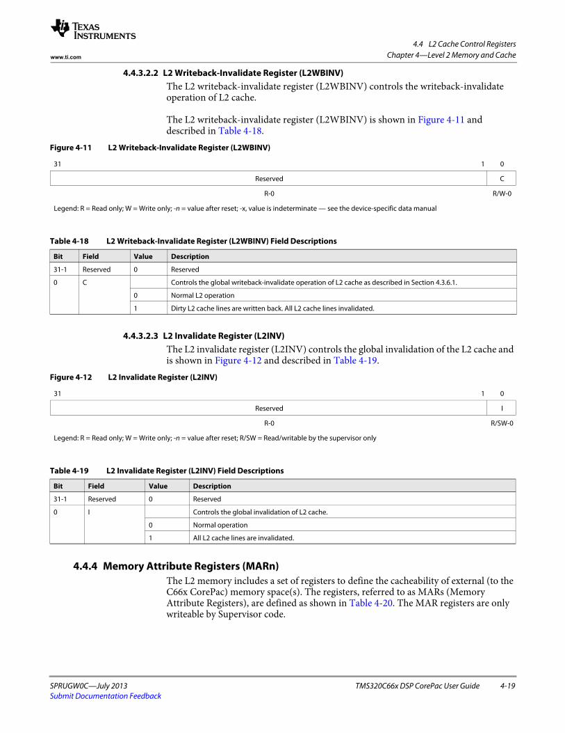
4.4 L2 Cache Control Registers
SPRUGW0C—July 2013 TMS320C66x DSP CorePac User Guide 4-19Submit Documentation Feedback
Chapter 4—Level 2 Memory and Cachewww.ti.com
4.4.3.2.2 L2 Writeback-Invalidate Register (L2WBINV)The L2 writeback-invalidate register (L2WBINV) controls the writeback-invalidate operation of L2 cache.
The L2 writeback-invalidate register (L2WBINV) is shown in Figure 4-11 and described in Table 4-18.
4.4.3.2.3 L2 Invalidate Register (L2INV)The L2 invalidate register (L2INV) controls the global invalidation of the L2 cache and is shown in Figure 4-12 and described in Table 4-19.
4.4.4 Memory Attribute Registers (MARn)The L2 memory includes a set of registers to define the cacheability of external (to the C66x CorePac) memory space(s). The registers, referred to as MARs (Memory Attribute Registers), are defined as shown in Table 4-20. The MAR registers are only writeable by Supervisor code.
Figure 4-11 L2 Writeback-Invalidate Register (L2WBINV)
31 1 0
Reserved C
R-0 R/W-0
Legend: R = Read only; W = Write only; -n = value after reset; -x, value is indeterminate — see the device-specific data manual
Table 4-18 L2 Writeback-Invalidate Register (L2WBINV) Field Descriptions
Bit Field Value Description
31-1 Reserved 0 Reserved
0 C Controls the global writeback-invalidate operation of L2 cache as described in Section 4.3.6.1.
0 Normal L2 operation
1 Dirty L2 cache lines are written back. All L2 cache lines invalidated.
Figure 4-12 L2 Invalidate Register (L2INV)
31 1 0
Reserved I
R-0 R/SW-0
Legend: R = Read only; W = Write only; -n = value after reset; R/SW = Read/writable by the supervisor only
Table 4-19 L2 Invalidate Register (L2INV) Field Descriptions
Bit Field Value Description
31-1 Reserved 0 Reserved
0 I Controls the global invalidation of L2 cache.
0 Normal operation
1 All L2 cache lines are invalidated.

4.4 L2 Cache Control Registers
4-20 TMS320C66x DSP CorePac User Guide SPRUGW0C—July 2013Submit Documentation Feedback
Chapter 4—Level 2 Memory and Cache www.ti.com
Table 4-20 below lists the memory attribute memory mapped control registers. The shaded portion in the table indicates MAR registers that are read-only Table 4-20 Memory Attribute Registers (Part 1 of 6)
Address Acronym Register Description Defines Attributes for. . .
0184 8000h MAR0 Memory Attribute Register 0 Local L2 RAM (fixed)
0184 8004h MAR1 Memory Attribute Register 1 0100 0000h - 01FF FFFFh
0184 8008h MAR2 Memory Attribute Register 2 0200 0000h - 02FF FFFFh
0184 800Ch MAR3 Memory Attribute Register 3 0300 0000h - 03FF FFFFh
0184 8010h MAR4 Memory Attribute Register 4 0400 0000h - 04FF FFFFh
0184 8014h MAR5 Memory Attribute Register 5 0500 0000h - 05FF FFFFh
0184 8018h MAR6 Memory Attribute Register 6 0600 0000h - 06FF FFFFh
0184 801Ch MAR7 Memory Attribute Register 7 0700 0000h - 07FF FFFFh
0184 8020h MAR8 Memory Attribute Register 8 0800 0000h - 08FF FFFFh
0184 8024h MAR9 Memory Attribute Register 9 0900 0000h - 09FF FFFFh
0184 8028h MAR10 Memory Attribute Register 10 0A00 0000h - 0AFF FFFFh
0184 802Ch MAR11 Memory Attribute Register 11 0B00 0000h - 0BFF FFFFh
0184 8030h MAR121 Memory Attribute Register 12 0C00 0000h - 0CFF FFFFh
0184 8034h MAR131 Memory Attribute Register 13 0D00 0000h - 0DFF FFFFh
0184 8038h MAR141 Memory Attribute Register 14 0E00 0000h - 0EFF FFFFh
0184 803Ch MAR151 Memory Attribute Register 15 0F00 0000h - 0FFF FFFFh
0184 8040h MAR16 Memory Attribute Register 16 1000 0000h - 10FF FFFFh
0184 8044h MAR17 Memory Attribute Register 17 1100 0000h - 11FF FFFFh
0184 8048h MAR18 Memory Attribute Register 18 1200 0000h - 12FF FFFFh
0184 804Ch MAR19 Memory Attribute Register 19 1300 0000h - 13FF FFFFh
0184 8050h MAR20 Memory Attribute Register 20 1400 0000h - 14FF FFFFh
0184 8054h MAR21 Memory Attribute Register 21 1500 0000h - 15FF FFFFh
0184 8058h MAR22 Memory Attribute Register 22 1600 0000h - 16FF FFFFh
0184 805Ch MAR23 Memory Attribute Register 23 1700 0000h - 17FF FFFFh
0184 8060h MAR24 Memory Attribute Register 24 1800 0000h - 18FF FFFFh
0184 8064h MAR25 Memory Attribute Register 25 1900 0000h - 19FF FFFFh
0184 8068h MAR26 Memory Attribute Register 26 1A00 0000h - 1AFF FFFFh
0184 806Ch MAR27 Memory Attribute Register 27 1B00 0000h - 1BFF FFFFh
0184 8070h MAR28 Memory Attribute Register 28 1C00 0000h - 1CFF FFFFh
0184 8074h MAR29 Memory Attribute Register 29 1D00 0000h - 1DFF FFFFh
0184 8078h MAR30 Memory Attribute Register 30 1E00 0000h - 1EFF FFFFh
0184 807Ch MAR31 Memory Attribute Register 31 1F00 0000h - 1FFF FFFFh
0184 8080h MAR32 Memory Attribute Register 32 2000 0000h - 20FF FFFFh
0184 8084h MAR33 Memory Attribute Register 33 2100 0000h - 21FF FFFFh
0184 8088h MAR34 Memory Attribute Register 34 2200 0000h - 22FF FFFFh
0184 808Ch MAR35 Memory Attribute Register 35 2300 0000h - 23FF FFFFh
0184 8090h MAR36 Memory Attribute Register 36 2400 0000h - 24FF FFFFh
0184 8094h MAR37 Memory Attribute Register 37 2500 0000h - 25FF FFFFh
0184 8098h MAR38 Memory Attribute Register 38 2600 0000h - 26FF FFFFh
0184 809Ch MAR39 Memory Attribute Register 39 2700 0000h - 27FF FFFFh
0184 80A0h MAR40 Memory Attribute Register 40 2800 0000h - 28FF FFFFh
0184 80A4h MAR41 Memory Attribute Register 41 2900 0000h - 29FF FFFFh
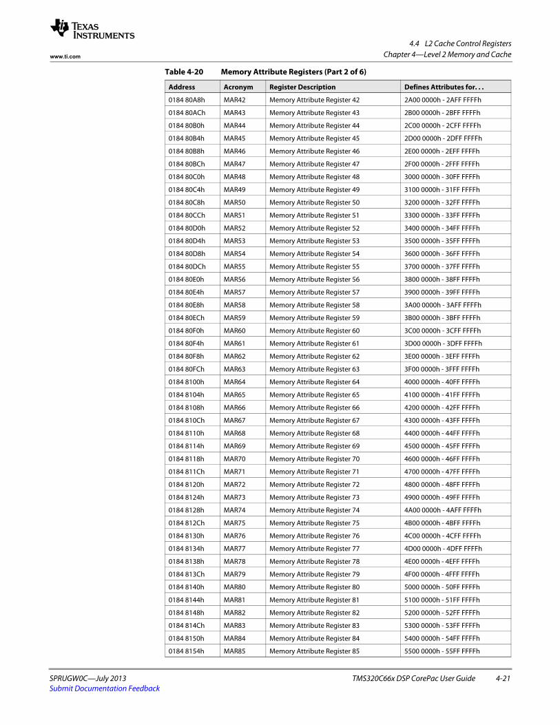
4.4 L2 Cache Control Registers
SPRUGW0C—July 2013 TMS320C66x DSP CorePac User Guide 4-21Submit Documentation Feedback
Chapter 4—Level 2 Memory and Cachewww.ti.com
0184 80A8h MAR42 Memory Attribute Register 42 2A00 0000h - 2AFF FFFFh
0184 80ACh MAR43 Memory Attribute Register 43 2B00 0000h - 2BFF FFFFh
0184 80B0h MAR44 Memory Attribute Register 44 2C00 0000h - 2CFF FFFFh
0184 80B4h MAR45 Memory Attribute Register 45 2D00 0000h - 2DFF FFFFh
0184 80B8h MAR46 Memory Attribute Register 46 2E00 0000h - 2EFF FFFFh
0184 80BCh MAR47 Memory Attribute Register 47 2F00 0000h - 2FFF FFFFh
0184 80C0h MAR48 Memory Attribute Register 48 3000 0000h - 30FF FFFFh
0184 80C4h MAR49 Memory Attribute Register 49 3100 0000h - 31FF FFFFh
0184 80C8h MAR50 Memory Attribute Register 50 3200 0000h - 32FF FFFFh
0184 80CCh MAR51 Memory Attribute Register 51 3300 0000h - 33FF FFFFh
0184 80D0h MAR52 Memory Attribute Register 52 3400 0000h - 34FF FFFFh
0184 80D4h MAR53 Memory Attribute Register 53 3500 0000h - 35FF FFFFh
0184 80D8h MAR54 Memory Attribute Register 54 3600 0000h - 36FF FFFFh
0184 80DCh MAR55 Memory Attribute Register 55 3700 0000h - 37FF FFFFh
0184 80E0h MAR56 Memory Attribute Register 56 3800 0000h - 38FF FFFFh
0184 80E4h MAR57 Memory Attribute Register 57 3900 0000h - 39FF FFFFh
0184 80E8h MAR58 Memory Attribute Register 58 3A00 0000h - 3AFF FFFFh
0184 80ECh MAR59 Memory Attribute Register 59 3B00 0000h - 3BFF FFFFh
0184 80F0h MAR60 Memory Attribute Register 60 3C00 0000h - 3CFF FFFFh
0184 80F4h MAR61 Memory Attribute Register 61 3D00 0000h - 3DFF FFFFh
0184 80F8h MAR62 Memory Attribute Register 62 3E00 0000h - 3EFF FFFFh
0184 80FCh MAR63 Memory Attribute Register 63 3F00 0000h - 3FFF FFFFh
0184 8100h MAR64 Memory Attribute Register 64 4000 0000h - 40FF FFFFh
0184 8104h MAR65 Memory Attribute Register 65 4100 0000h - 41FF FFFFh
0184 8108h MAR66 Memory Attribute Register 66 4200 0000h - 42FF FFFFh
0184 810Ch MAR67 Memory Attribute Register 67 4300 0000h - 43FF FFFFh
0184 8110h MAR68 Memory Attribute Register 68 4400 0000h - 44FF FFFFh
0184 8114h MAR69 Memory Attribute Register 69 4500 0000h - 45FF FFFFh
0184 8118h MAR70 Memory Attribute Register 70 4600 0000h - 46FF FFFFh
0184 811Ch MAR71 Memory Attribute Register 71 4700 0000h - 47FF FFFFh
0184 8120h MAR72 Memory Attribute Register 72 4800 0000h - 48FF FFFFh
0184 8124h MAR73 Memory Attribute Register 73 4900 0000h - 49FF FFFFh
0184 8128h MAR74 Memory Attribute Register 74 4A00 0000h - 4AFF FFFFh
0184 812Ch MAR75 Memory Attribute Register 75 4B00 0000h - 4BFF FFFFh
0184 8130h MAR76 Memory Attribute Register 76 4C00 0000h - 4CFF FFFFh
0184 8134h MAR77 Memory Attribute Register 77 4D00 0000h - 4DFF FFFFh
0184 8138h MAR78 Memory Attribute Register 78 4E00 0000h - 4EFF FFFFh
0184 813Ch MAR79 Memory Attribute Register 79 4F00 0000h - 4FFF FFFFh
0184 8140h MAR80 Memory Attribute Register 80 5000 0000h - 50FF FFFFh
0184 8144h MAR81 Memory Attribute Register 81 5100 0000h - 51FF FFFFh
0184 8148h MAR82 Memory Attribute Register 82 5200 0000h - 52FF FFFFh
0184 814Ch MAR83 Memory Attribute Register 83 5300 0000h - 53FF FFFFh
0184 8150h MAR84 Memory Attribute Register 84 5400 0000h - 54FF FFFFh
0184 8154h MAR85 Memory Attribute Register 85 5500 0000h - 55FF FFFFh
Table 4-20 Memory Attribute Registers (Part 2 of 6)
Address Acronym Register Description Defines Attributes for. . .
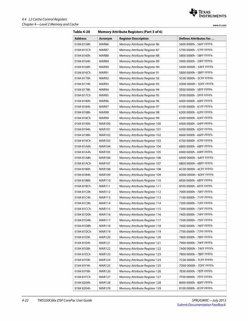
4.4 L2 Cache Control Registers
4-22 TMS320C66x DSP CorePac User Guide SPRUGW0C—July 2013Submit Documentation Feedback
Chapter 4—Level 2 Memory and Cache www.ti.com
0184 8158h MAR86 Memory Attribute Register 86 5600 0000h - 56FF FFFFh
0184 815Ch MAR87 Memory Attribute Register 87 5700 0000h - 57FF FFFFh
0184 8160h MAR88 Memory Attribute Register 88 5800 0000h - 58FF FFFFh
0184 8164h MAR89 Memory Attribute Register 89 5900 0000h - 59FF FFFFh
0184 8168h MAR90 Memory Attribute Register 90 5A00 0000h - 5AFF FFFFh
0184 816Ch MAR91 Memory Attribute Register 91 5B00 0000h - 5BFF FFFFh
0184 8170h MAR92 Memory Attribute Register 92 5C00 0000h - 5CFF FFFFh
0184 8174h MAR93 Memory Attribute Register 93 5D00 0000h - 5DFF FFFFh
0184 8178h MAR94 Memory Attribute Register 94 5E00 0000h - 5EFF FFFFh
0184 817Ch MAR95 Memory Attribute Register 95 5F00 0000h - 5FFF FFFFh
0184 8180h MAR96 Memory Attribute Register 96 6000 0000h - 60FF FFFFh
0184 8184h MAR97 Memory Attribute Register 97 6100 0000h - 61FF FFFFh
0184 8188h MAR98 Memory Attribute Register 98 6200 0000h - 62FF FFFFh
0184 818Ch MAR99 Memory Attribute Register 99 6300 0000h - 63FF FFFFh
0184 8190h MAR100 Memory Attribute Register 100 6400 0000h - 64FF FFFFh
0184 8194h MAR101 Memory Attribute Register 101 6500 0000h - 65FF FFFFh
0184 8198h MAR102 Memory Attribute Register 102 6600 0000h - 66FF FFFFh
0184 819Ch MAR103 Memory Attribute Register 103 6700 0000h - 67FF FFFFh
0184 81A0h MAR104 Memory Attribute Register 104 6800 0000h - 68FF FFFFh
0184 81A4h MAR105 Memory Attribute Register 105 6900 0000h - 69FF FFFFh
0184 81A8h MAR106 Memory Attribute Register 106 6A00 0000h - 6AFF FFFFh
0184 81ACh MAR107 Memory Attribute Register 107 6B00 0000h - 6BFF FFFFh
0184 81B0h MAR108 Memory Attribute Register 108 6C00 0000h - 6CFF FFFFh
0184 81B4h MAR109 Memory Attribute Register 109 6D00 0000h - 6DFF FFFFh
0184 81B8h MAR110 Memory Attribute Register 110 6E00 0000h - 6EFF FFFFh
0184 81BCh MAR111 Memory Attribute Register 111 6F00 0000h - 6FFF FFFFh
0184 81C0h MAR112 Memory Attribute Register 112 7000 0000h - 70FF FFFFh
0184 81C4h MAR113 Memory Attribute Register 113 7100 0000h - 71FF FFFFh
0184 81C8h MAR114 Memory Attribute Register 114 7200 0000h - 72FF FFFFh
0184 81CCh MAR115 Memory Attribute Register 115 7300 0000h - 73FF FFFFh
0184 81D0h MAR116 Memory Attribute Register 116 7400 0000h - 74FF FFFFh
0184 81D4h MAR117 Memory Attribute Register 117 7500 0000h - 75FF FFFFh
0184 81D8h MAR118 Memory Attribute Register 118 7600 0000h - 76FF FFFFh
0184 81DCh MAR119 Memory Attribute Register 119 7700 0000h - 77FF FFFFh
0184 81E0h MAR120 Memory Attribute Register 120 7800 0000h - 78FF FFFFh
0184 81E4h MAR121 Memory Attribute Register 121 7900 0000h - 79FF FFFFh
0184 81E8h MAR122 Memory Attribute Register 122 7A00 0000h - 7AFF FFFFh
0184 81ECh MAR123 Memory Attribute Register 123 7B00 0000h - 7BFF FFFFh
0184 81F0h MAR124 Memory Attribute Register 124 7C00 0000h - 7CFF FFFFh
0184 81F4h MAR125 Memory Attribute Register 125 7D00 0000h - 7DFF FFFFh
0184 81F8h MAR126 Memory Attribute Register 126 7E00 0000h - 7EFF FFFFh
0184 81FCh MAR127 Memory Attribute Register 127 7F00 0000h - 7FFF FFFFh
0184 8200h MAR128 Memory Attribute Register 128 8000 0000h - 80FF FFFFh
0184 8204h MAR129 Memory Attribute Register 129 8100 0000h - 81FF FFFFh
Table 4-20 Memory Attribute Registers (Part 3 of 6)
Address Acronym Register Description Defines Attributes for. . .
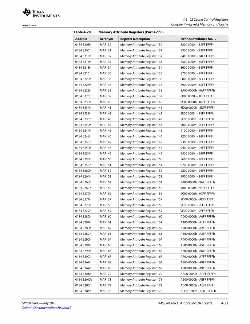
4.4 L2 Cache Control Registers
SPRUGW0C—July 2013 TMS320C66x DSP CorePac User Guide 4-23Submit Documentation Feedback
Chapter 4—Level 2 Memory and Cachewww.ti.com
0184 8208h MAR130 Memory Attribute Register 130 8200 0000h - 82FF FFFFh
0184 820Ch MAR131 Memory Attribute Register 131 8300 0000h - 83FF FFFFh
0184 8210h MAR132 Memory Attribute Register 132 8400 0000h - 84FF FFFFh
0184 8214h MAR133 Memory Attribute Register 133 8500 0000h - 85FF FFFFh
0184 8218h MAR134 Memory Attribute Register 134 8600 0000h - 86FF FFFFh
0184 821Ch MAR135 Memory Attribute Register 135 8700 0000h - 87FF FFFFh
0184 8220h MAR136 Memory Attribute Register 136 8800 0000h - 88FF FFFFh
0184 8224h MAR137 Memory Attribute Register 137 8900 0000h - 89FF FFFFh
0184 8228h MAR138 Memory Attribute Register 138 8A00 0000h - 8AFF FFFFh
0184 822Ch MAR139 Memory Attribute Register 139 8B00 0000h - 8BFF FFFFh
0184 8230h MAR140 Memory Attribute Register 140 8C00 0000h - 8CFF FFFFh
0184 8234h MAR141 Memory Attribute Register 141 8D00 0000h - 8DFF FFFFh
0184 8238h MAR142 Memory Attribute Register 142 8E00 0000h - 8EFF FFFFh
0184 823Ch MAR143 Memory Attribute Register 143 8F00 0000h - 8FFF FFFFh
0184 8240h MAR144 Memory Attribute Register 144 9000 0000h - 90FF FFFFh
0184 8244h MAR145 Memory Attribute Register 145 9100 0000h - 91FF FFFFh
0184 8248h MAR146 Memory Attribute Register 146 9200 0000h - 92FF FFFFh
0184 824Ch MAR147 Memory Attribute Register 147 9300 0000h - 93FF FFFFh
0184 8250h MAR148 Memory Attribute Register 148 9400 0000h - 94FF FFFFh
0184 8254h MAR149 Memory Attribute Register 149 9500 0000h - 95FF FFFFh
0184 8258h MAR150 Memory Attribute Register 150 9600 0000h - 96FF FFFFh
0184 825Ch MAR151 Memory Attribute Register 151 9700 0000h - 97FF FFFFh
0184 8260h MAR152 Memory Attribute Register 152 9800 0000h - 98FF FFFFh
0184 8264h MAR153 Memory Attribute Register 153 9900 0000h - 99FF FFFFh
0184 8268h MAR154 Memory Attribute Register 154 9A00 0000h - 9AFF FFFFh
0184 826Ch MAR155 Memory Attribute Register 155 9B00 0000h - 9BFF FFFFh
0184 8270h MAR156 Memory Attribute Register 156 9C00 0000h - 9CFF FFFFh
0184 8274h MAR157 Memory Attribute Register 157 9D00 0000h - 9DFF FFFFh
0184 8278h MAR158 Memory Attribute Register 158 9E00 0000h - 9EFF FFFFh
0184 827Ch MAR159 Memory Attribute Register 159 9F00 0000h - 9FFF FFFFh
0184 8280h MAR160 Memory Attribute Register 160 A000 0000h - A0FF FFFFh
0184 8284h MAR161 Memory Attribute Register 161 A100 0000h - A1FF FFFFh
0184 8288h MAR162 Memory Attribute Register 162 A200 0000h - A2FF FFFFh
0184 828Ch MAR163 Memory Attribute Register 163 A300 0000h - A3FF FFFFh
0184 8290h MAR164 Memory Attribute Register 164 A400 0000h - A4FF FFFFh
0184 8294h MAR165 Memory Attribute Register 165 A500 0000h - A5FF FFFFh
0184 8298h MAR166 Memory Attribute Register 166 A600 0000h - A6FF FFFFh
0184 829Ch MAR167 Memory Attribute Register 167 A700 0000h - A7FF FFFFh
0184 82A0h MAR168 Memory Attribute Register 168 A800 0000h - A8FF FFFFh
0184 82A4h MAR169 Memory Attribute Register 169 A900 0000h - A9FF FFFFh
0184 82A8h MAR170 Memory Attribute Register 170 AA00 0000h - AAFF FFFFh
0184 82ACh MAR171 Memory Attribute Register 171 AB00 0000h - ABFF FFFFh
0184 82B0h MAR172 Memory Attribute Register 172 AC00 0000h - ACFF FFFFh
0184 82B4h MAR173 Memory Attribute Register 173 AD00 0000h - ADFF FFFFh
Table 4-20 Memory Attribute Registers (Part 4 of 6)
Address Acronym Register Description Defines Attributes for. . .

4.4 L2 Cache Control Registers
4-24 TMS320C66x DSP CorePac User Guide SPRUGW0C—July 2013Submit Documentation Feedback
Chapter 4—Level 2 Memory and Cache www.ti.com
0184 82B8h MAR174 Memory Attribute Register 174 AE00 0000h - AEFF FFFFh
0184 82BCh MAR175 Memory Attribute Register 175 AF00 0000h - AFFF FFFFh
0184 82C0h MAR176 Memory Attribute Register 176 B000 0000h - B0FF FFFFh
0184 82C4h MAR177 Memory Attribute Register 177 B100 0000h - B1FF FFFFh
0184 82C8h MAR178 Memory Attribute Register 178 B200 0000h - B2FF FFFFh
0184 82CCh MAR179 Memory Attribute Register 179 B300 0000h - B3FF FFFFh
0184 82D0h MAR180 Memory Attribute Register 180 B400 0000h - B4FF FFFFh
0184 82D4h MAR181 Memory Attribute Register 181 B500 0000h - B5FF FFFFh
0184 82D8h MAR182 Memory Attribute Register 182 B600 0000h - B6FF FFFFh
0184 82DCh MAR183 Memory Attribute Register 183 B700 0000h - B7FF FFFFh
0184 82E0h MAR184 Memory Attribute Register 184 B800 0000h - B8FF FFFFh
0184 82E4h MAR185 Memory Attribute Register 185 B900 0000h - B9FF FFFFh
0184 82E8h MAR186 Memory Attribute Register 186 BA00 0000h - BAFF FFFFh
0184 82ECh MAR187 Memory Attribute Register 187 BB00 0000h - BBFF FFFFh
0184 82F0h MAR188 Memory Attribute Register 188 BC00 0000h - BCFF FFFFh
0184 82F4h MAR189 Memory Attribute Register 189 BD00 0000h - BDFF FFFFh
0184 82F8h MAR190 Memory Attribute Register 190 BE00 0000h - BEFF FFFFh
0184 82FCh MAR191 Memory Attribute Register 191 BF00 0000h - BFFF FFFFh
0184 8300h MAR192 Memory Attribute Register 192 C000 0000h - C0FF FFFFh
0184 8304h MAR193 Memory Attribute Register 193 C100 0000h - C1FF FFFFh
0184 8308h MAR194 Memory Attribute Register 194 C200 0000h - C2FF FFFFh
0184 830Ch MAR195 Memory Attribute Register 195 C300 0000h - C3FF FFFFh
0184 8310h MAR196 Memory Attribute Register 196 C400 0000h - C4FF FFFFh
0184 8314h MAR197 Memory Attribute Register 197 C500 0000h - C5FF FFFFh
0184 8318h MAR198 Memory Attribute Register 198 C600 0000h - C6FF FFFFh
0184 831Ch MAR199 Memory Attribute Register 199 C700 0000h - C7FF FFFFh
0184 8320h MAR200 Memory Attribute Register 200 C800 0000h - C8FF FFFFh
0184 8324h MAR201 Memory Attribute Register 201 C900 0000h - C9FF FFFFh
0184 8328h MAR202 Memory Attribute Register 202 CA00 0000h - CAFF FFFFh
0184 832Ch MAR203 Memory Attribute Register 203 CB00 0000h - CBFF FFFFh
0184 8330h MAR204 Memory Attribute Register 204 CC00 0000h - CCFF FFFFh
0184 8334h MAR205 Memory Attribute Register 205 CD00 0000h - CDFF FFFFh
0184 8338h MAR206 Memory Attribute Register 206 CE00 0000h - CEFF FFFFh
0184 833Ch MAR207 Memory Attribute Register 207 CF00 0000h - CFFF FFFFh
0184 8340h MAR208 Memory Attribute Register 208 D000 0000h - D0FF FFFFh
0184 8344h MAR209 Memory Attribute Register 209 D100 0000h - D1FF FFFFh
0184 8348h MAR210 Memory Attribute Register 210 D200 0000h - D2FF FFFFh
0184 834Ch MAR211 Memory Attribute Register 211 D300 0000h - D3FF FFFFh
0184 8350h MAR212 Memory Attribute Register 212 D400 0000h - D4FF FFFFh
0184 8354h MAR213 Memory Attribute Register 213 D500 0000h - D5FF FFFFh
0184 8358h MAR214 Memory Attribute Register 214 D600 0000h - D6FF FFFFh
0184 835Ch MAR215 Memory Attribute Register 215 D700 0000h - D7FF FFFFh
0184 8360h MAR216 Memory Attribute Register 216 D800 0000h - D8FF FFFFh
0184 8364h MAR217 Memory Attribute Register 217 D900 0000h - D9FF FFFFh
Table 4-20 Memory Attribute Registers (Part 5 of 6)
Address Acronym Register Description Defines Attributes for. . .
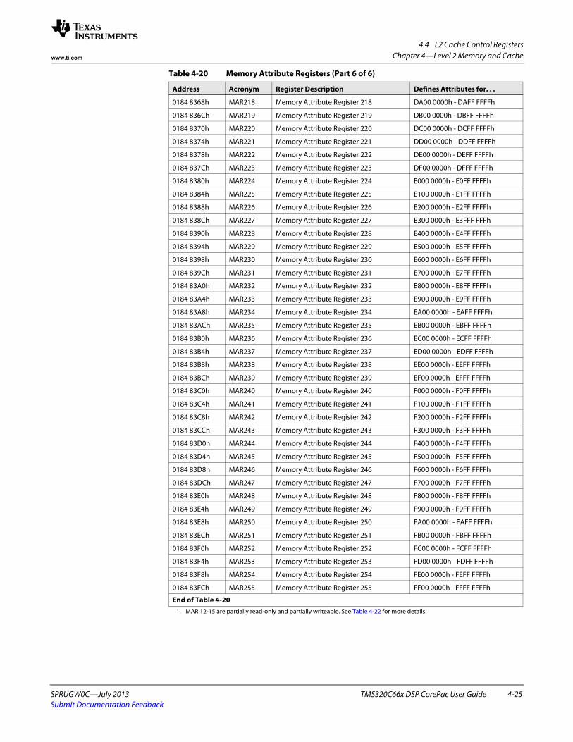
4.4 L2 Cache Control Registers
SPRUGW0C—July 2013 TMS320C66x DSP CorePac User Guide 4-25Submit Documentation Feedback
Chapter 4—Level 2 Memory and Cachewww.ti.com
0184 8368h MAR218 Memory Attribute Register 218 DA00 0000h - DAFF FFFFh
0184 836Ch MAR219 Memory Attribute Register 219 DB00 0000h - DBFF FFFFh
0184 8370h MAR220 Memory Attribute Register 220 DC00 0000h - DCFF FFFFh
0184 8374h MAR221 Memory Attribute Register 221 DD00 0000h - DDFF FFFFh
0184 8378h MAR222 Memory Attribute Register 222 DE00 0000h - DEFF FFFFh
0184 837Ch MAR223 Memory Attribute Register 223 DF00 0000h - DFFF FFFFh
0184 8380h MAR224 Memory Attribute Register 224 E000 0000h - E0FF FFFFh
0184 8384h MAR225 Memory Attribute Register 225 E100 0000h - E1FF FFFFh
0184 8388h MAR226 Memory Attribute Register 226 E200 0000h - E2FF FFFFh
0184 838Ch MAR227 Memory Attribute Register 227 E300 0000h - E3FFF FFFh
0184 8390h MAR228 Memory Attribute Register 228 E400 0000h - E4FF FFFFh
0184 8394h MAR229 Memory Attribute Register 229 E500 0000h - E5FF FFFFh
0184 8398h MAR230 Memory Attribute Register 230 E600 0000h - E6FF FFFFh
0184 839Ch MAR231 Memory Attribute Register 231 E700 0000h - E7FF FFFFh
0184 83A0h MAR232 Memory Attribute Register 232 E800 0000h - E8FF FFFFh
0184 83A4h MAR233 Memory Attribute Register 233 E900 0000h - E9FF FFFFh
0184 83A8h MAR234 Memory Attribute Register 234 EA00 0000h - EAFF FFFFh
0184 83ACh MAR235 Memory Attribute Register 235 EB00 0000h - EBFF FFFFh
0184 83B0h MAR236 Memory Attribute Register 236 EC00 0000h - ECFF FFFFh
0184 83B4h MAR237 Memory Attribute Register 237 ED00 0000h - EDFF FFFFh
0184 83B8h MAR238 Memory Attribute Register 238 EE00 0000h - EEFF FFFFh
0184 83BCh MAR239 Memory Attribute Register 239 EF00 0000h - EFFF FFFFh
0184 83C0h MAR240 Memory Attribute Register 240 F000 0000h - F0FF FFFFh
0184 83C4h MAR241 Memory Attribute Register 241 F100 0000h - F1FF FFFFh
0184 83C8h MAR242 Memory Attribute Register 242 F200 0000h - F2FF FFFFh
0184 83CCh MAR243 Memory Attribute Register 243 F300 0000h - F3FF FFFFh
0184 83D0h MAR244 Memory Attribute Register 244 F400 0000h - F4FF FFFFh
0184 83D4h MAR245 Memory Attribute Register 245 F500 0000h - F5FF FFFFh
0184 83D8h MAR246 Memory Attribute Register 246 F600 0000h - F6FF FFFFh
0184 83DCh MAR247 Memory Attribute Register 247 F700 0000h - F7FF FFFFh
0184 83E0h MAR248 Memory Attribute Register 248 F800 0000h - F8FF FFFFh
0184 83E4h MAR249 Memory Attribute Register 249 F900 0000h - F9FF FFFFh
0184 83E8h MAR250 Memory Attribute Register 250 FA00 0000h - FAFF FFFFh
0184 83ECh MAR251 Memory Attribute Register 251 FB00 0000h - FBFF FFFFh
0184 83F0h MAR252 Memory Attribute Register 252 FC00 0000h - FCFF FFFFh
0184 83F4h MAR253 Memory Attribute Register 253 FD00 0000h - FDFF FFFFh
0184 83F8h MAR254 Memory Attribute Register 254 FE00 0000h - FEFF FFFFh
0184 83FCh MAR255 Memory Attribute Register 255 FF00 0000h - FFFF FFFFh
End of Table 4-201. MAR 12-15 are partially read-only and partially writeable. See Table 4-22 for more details.
Table 4-20 Memory Attribute Registers (Part 6 of 6)
Address Acronym Register Description Defines Attributes for. . .
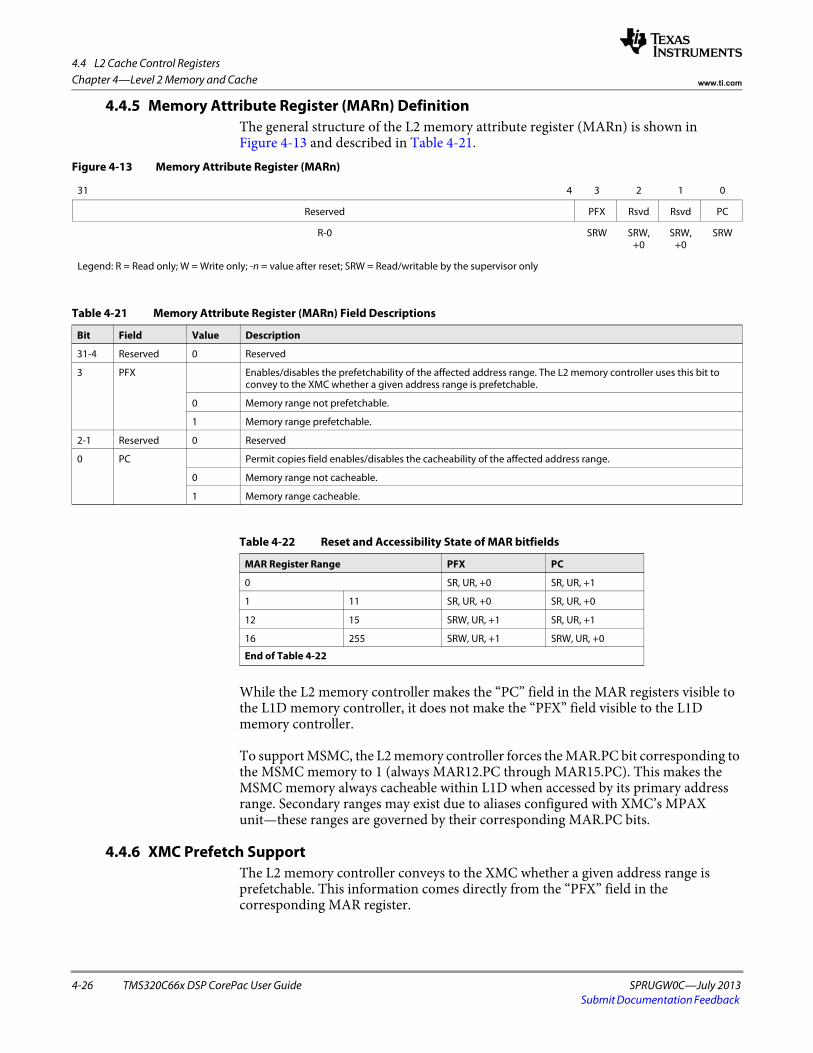
4.4 L2 Cache Control Registers
4-26 TMS320C66x DSP CorePac User Guide SPRUGW0C—July 2013Submit Documentation Feedback
Chapter 4—Level 2 Memory and Cache www.ti.com
4.4.5 Memory Attribute Register (MARn) DefinitionThe general structure of the L2 memory attribute register (MARn) is shown in Figure 4-13 and described in Table 4-21.
While the L2 memory controller makes the “PC” field in the MAR registers visible to the L1D memory controller, it does not make the “PFX” field visible to the L1D memory controller.
To support MSMC, the L2 memory controller forces the MAR.PC bit corresponding to the MSMC memory to 1 (always MAR12.PC through MAR15.PC). This makes the MSMC memory always cacheable within L1D when accessed by its primary address range. Secondary ranges may exist due to aliases configured with XMC’s MPAX unit—these ranges are governed by their corresponding MAR.PC bits.
4.4.6 XMC Prefetch SupportThe L2 memory controller conveys to the XMC whether a given address range is prefetchable. This information comes directly from the “PFX” field in the corresponding MAR register.
Figure 4-13 Memory Attribute Register (MARn)
31 4 3 2 1 0
Reserved PFX Rsvd Rsvd PC
R-0 SRW SRW, +0
SRW, +0
SRW
Legend: R = Read only; W = Write only; -n = value after reset; SRW = Read/writable by the supervisor only
Table 4-21 Memory Attribute Register (MARn) Field Descriptions
Bit Field Value Description
31-4 Reserved 0 Reserved
3 PFX Enables/disables the prefetchability of the affected address range. The L2 memory controller uses this bit to convey to the XMC whether a given address range is prefetchable.
0 Memory range not prefetchable.
1 Memory range prefetchable.
2-1 Reserved 0 Reserved
0 PC Permit copies field enables/disables the cacheability of the affected address range.
0 Memory range not cacheable.
1 Memory range cacheable.
Table 4-22 Reset and Accessibility State of MAR bitfields
MAR Register Range PFX PC
0 SR, UR, +0 SR, UR, +1
1 11 SR, UR, +0 SR, UR, +0
12 15 SRW, UR, +1 SR, UR, +1
16 255 SRW, UR, +1 SRW, UR, +0
End of Table 4-22
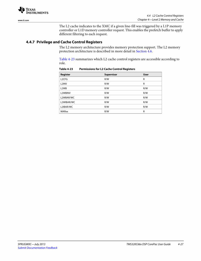
4.4 L2 Cache Control Registers
SPRUGW0C—July 2013 TMS320C66x DSP CorePac User Guide 4-27Submit Documentation Feedback
Chapter 4—Level 2 Memory and Cachewww.ti.com
The L2 cache indicates to the XMC if a given line-fill was triggered by a L1P memory controller or L1D memory controller request. This enables the prefetch buffer to apply different filtering to each request.
4.4.7 Privilege and Cache Control RegistersThe L2 memory architecture provides memory protection support. The L2 memory protection architecture is described in more detail in Section 4.6.
Table 4-23 summarizes which L2 cache control registers are accessible according to role.Table 4-23 Permissions for L2 Cache Control Registers
Register Supervisor User
L2CFG R/W R
L2INV R/W R
L2WB R/W R/W
L2WBINV R/W R/W
L2WBAR/WC R/W R/W
L2WIBAR/WC R/W R/W
L2IBAR/WC R/W R/W
MARxx R/W R

4.5 L2 Power-Down
4-28 TMS320C66x DSP CorePac User Guide SPRUGW0C—July 2013Submit Documentation Feedback
Chapter 4—Level 2 Memory and Cache www.ti.com
4.5 L2 Power-DownThe C66x CorePac architecture provides several power-down features. Some features are transparent. Others are controlled through software. The power-down features can be divided into two groups: dynamic and static. Dynamic power-down features are used at run-time for a limited period of time, whereas static power-down features are used for a longer period of time when the DSP is in idle mode. These power-down features are controlled through registers that are local to the specific module or part of the power-down controller (PDC). Read Chapter 12 on page 12-1 prior to reading this section in order to understand this section better.
4.5.1 L2 Memory Static Power-Down The C66x CorePac provides support for static power-down of L2 memory. The L2 memory can be powered-down when the entire C66x CorePac is powered-down. The following software sequence is required to power-down the C66x CorePac:
1. Set the MEGPD field in the PDCCMD register to 1 to enable power-down mode.2. Enable the DSP interrupt(s) that you want to wake the C66x CorePac up; disable
all others.3. Execute an IDLE instruction.
The C66x CorePac stays in powered-down until awakened by the interrupt(s) enabled in step 2, above.
If a DMA access occurs to the L1D, L1P, or L2 memory while the C66x CorePac is powered-down, the PDC wakes all three memory controllers. When the DMA access has been serviced, the PDC will again power-down the memory controllers.
Note—Powering-down the C66x CorePac as described here is often called static power-down. This term is used to describe this mode since it is often used for longer periods of time.
See Chapter 12 on page 12-1 for more information about the PDCCMD register and the power-down capabilities of the C66x CorePac.
4.5.2 L2 Memory Dynamic Power-Down The C66x CorePac does not support user-controlled dynamic power-down of L2 memory. In KeyStone devices, Retention Until Access (RTA) memories are used as L2 memory. This memory is always in a low leakage mode and wakes up only a block of memory that is accessed and that block is put back into the low leakage mode again. So the L2 memory itself takes care of dynamic page based wakeup automatically.

4.6 L2 Memory Protection
SPRUGW0C—July 2013 TMS320C66x DSP CorePac User Guide 4-29Submit Documentation Feedback
Chapter 4—Level 2 Memory and Cachewww.ti.com
4.6 L2 Memory ProtectionL2 memory supports memory protection to offer the robustness required in many systems. Several levels of memory protection are available. Not all the levels are available on all the devices. See the device-specific data manual for more information. Familiarize yourself with Chapter 10 on page 10-1 before reading this section.
4.6.1 Protection Checks on DSP, IDMA and Other System Master AccessesMemory protection checks are performed for accesses that are serviced directly by the L2 from L1P, L1D, IDMA, and other system masters on devices that include memory protection support.
The L2 memory controller feature two exception outputs that are routed to the C66x CorePac interrupt controller. One of these exception outputs indicates that a DSP-triggered “local” memory exception (L2_CMPA) occurred. The other indicates that a system master-triggered “remote” exception (L2_DMPA) occurred. It is expected that most programs route the DSP-triggered exception input to the DSP’s exception input and the system master triggered input to an interrupt input.
L2 does not perform protection checks on DSP reads that arrive in L2, regardless of whether they hit or miss in L2. Reads ultimately return the access permissions to the requestor, thereby deferring the check to L1D or L1P. In contrast, L2 checks all DSP writes that hit L2, or that miss L2 and subsequently allocate a line in the L2 cache. L2 does not check permissions on non-cacheable writes that miss L2. Therefore, L2 checks all DSP accesses that end at L2, and defers checks for other access to the controller (L1P, L1D, or external peripheral) that ultimately services the access.
All system masters and IDMA accesses (reads and writes) to L2 memory are always checked. System masters and IDMA accesses to addresses held in L2 cache are not checked. L2 (or EMC) performs protection checks before issuing snoop-write commands to L1D for addresses held in L1D cache.
The L2 controller determines whether a given request is allowed or not allowed based on the privilege associated with the request, and the permission settings on the address range that the request accesses. Chapter 10 on page 10-1 sets the exact rules for these checks forth.
L2 asserts an exception and denies the request if a given request has insufficient permission. Reads that are not allowed return garbage and writes that are not allowed are killed before the underlying memory is written. The L2 only permission-checks DSP writes that miss L2 if they are cacheable within L2 or later stages of the memory system if they are not cacheable.
4.6.2 L2 Memory Protection RegistersThe following registers govern the operation of L2 memory protection. The registers fall into three main categories:
• Memory Protection Page Attribute (MPPA) registers. These registers store the permissions associated with each protected page.
• Memory Protection Lock Registers (MPLK): Memory Controllers may choose to implement a hardware memory protection lock. When engaged, the lock disables all updates to the memory protection entries for all four memory controllers (L1P, L1D, L2 and XMC).
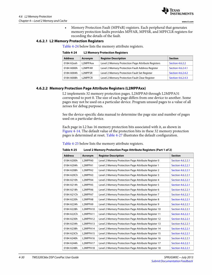
4.6 L2 Memory Protection
4-30 TMS320C66x DSP CorePac User Guide SPRUGW0C—July 2013Submit Documentation Feedback
Chapter 4—Level 2 Memory and Cache www.ti.com
• Memory Protection Fault (MPFxR) registers. Each peripheral that generates memory protection faults provides MPFAR, MPFSR, and MPFCLR registers for recording the details of the fault.
4.6.2.1 L2 Memory Protection RegistersTable 4-24 below lists the memory attribute registers.
4.6.2.2 Memory Protection Page Attribute Registers (L2MPPAxx)L2 implements 32 memory protection pages. L2MPPA0 through L2MPPA31 correspond to port 0. The size of each page differs from one device to another. Some pages may not be used on a particular device. Program unused pages to a value of all zeroes for debug purposes.
See the device-specific data manual to determine the page size and number of pages used on a particular device.
Each page in L2 has 16 memory protection bits associated with it, as shown in Figure 4-14. The default value of the protection bits in these 32 memory protection pages is determined at reset. Table 4-27 illustrates the default configuration.
Table 4-25 below lists the memory attribute registers.
Table 4-24 L2 Memory Protection Registers
Address Acronym Register Description Section
0184 A2xxh L2MPPAxx Level 2 Memory Protection Page Attribute Registers Section 4.6.2.2
0184 A000h L2MPFAR Level 2 Memory Protection Fault Address Register Section 4.6.2.4.1
0184 A004h L2MPFSR Level 2 Memory Protection Fault Set Register Section 4.6.2.4.2
0184 A008h L2MPFCR Level 2 Memory Protection Fault Clear Register Section 4.6.2.4.3
Table 4-25 Level 2 Memory Protection Page Attribute Registers (Part 1 of 2)
Address Acronym Register Description Section
0184 A200h L2MPPA0 Level 2 Memory Protection Page Attribute Register 0 Section 4.6.2.2.1
0184 A204h L2MPPA1 Level 2 Memory Protection Page Attribute Register 1 Section 4.6.2.2.1
0184 A208h L2MPPA2 Level 2 Memory Protection Page Attribute Register 2 Section 4.6.2.2.1
0184 A20Ch L2MPPA3 Level 2 Memory Protection Page Attribute Register 3 Section 4.6.2.2.1
0184 A210h L2MPPA4 Level 2 Memory Protection Page Attribute Register 4 Section 4.6.2.2.1
0184 A214h L2MPPA5 Level 2 Memory Protection Page Attribute Register 5 Section 4.6.2.2.1
0184 A218h L2MPPA6 Level 2 Memory Protection Page Attribute Register 6 Section 4.6.2.2.1
0184 A21Ch L2MPPA7 Level 2 Memory Protection Page Attribute Register 7 Section 4.6.2.2.1
0184 A220h L2MPPA8 Level 2 Memory Protection Page Attribute Register 8 Section 4.6.2.2.1
0184 A224h L2MPPA9 Level 2 Memory Protection Page Attribute Register 9 Section 4.6.2.2.1
0184 A228h L2MPPA10 Level 2 Memory Protection Page Attribute Register 10 Section 4.6.2.2.1
0184 A22Ch L2MPPA11 Level 2 Memory Protection Page Attribute Register 11 Section 4.6.2.2.1
0184 A230h L2MPPA12 Level 2 Memory Protection Page Attribute Register 12 Section 4.6.2.2.1
0184 A234h L2MPPA13 Level 2 Memory Protection Page Attribute Register 13 Section 4.6.2.2.1
0184 A238h L2MPPA14 Level 2 Memory Protection Page Attribute Register 14 Section 4.6.2.2.1
0184 A23Ch L2MPPA15 Level 2 Memory Protection Page Attribute Register 15 Section 4.6.2.2.1
0184 A240h L2MPPA16 Level 2 Memory Protection Page Attribute Register 16 Section 4.6.2.2.1
0184 A244h L2MPPA17 Level 2 Memory Protection Page Attribute Register 17 Section 4.6.2.2.1
0184 A248h L2MPPA18 Level 2 Memory Protection Page Attribute Register 18 Section 4.6.2.2.1

4.6 L2 Memory Protection
SPRUGW0C—July 2013 TMS320C66x DSP CorePac User Guide 4-31Submit Documentation Feedback
Chapter 4—Level 2 Memory and Cachewww.ti.com
4.6.2.2.1 Memory Protection Page Attribute Registers (L2MPPAn)The level 2 memory protection page attribute registers (L2MPPAn) are shown in Figure 4-14 and described in Table 4-26.
0184 A24Ch L2MPPA19 Level 2 Memory Protection Page Attribute Register 19 Section 4.6.2.2.1
0184 A250h L2MPPA20 Level 2 Memory Protection Page Attribute Register 20 Section 4.6.2.2.1
0184 A254h L2MPPA21 Level 2 Memory Protection Page Attribute Register 21 Section 4.6.2.2.1
0184 A258h L2MPPA22 Level 2 Memory Protection Page Attribute Register 22 Section 4.6.2.2.1
0184 A25Ch L2MPPA23 Level 2 Memory Protection Page Attribute Register 23 Section 4.6.2.2.1
0184 A260h L2MPPA24 Level 2 Memory Protection Page Attribute Register 24 Section 4.6.2.2.1
0184 A264h L2MPPA25 Level 2 Memory Protection Page Attribute Register 25 Section 4.6.2.2.1
0184 A268h L2MPPA26 Level 2 Memory Protection Page Attribute Register 26 Section 4.6.2.2.1
0184 A26Ch L2MPPA27 Level 2 Memory Protection Page Attribute Register 27 Section 4.6.2.2.1
0184 A270h L2MPPA28 Level 2 Memory Protection Page Attribute Register 28 Section 4.6.2.2.1
0184 A274h L2MPPA29 Level 2 Memory Protection Page Attribute Register 29 Section 4.6.2.2.1
0184 A278h L2MPPA30 Level 2 Memory Protection Page Attribute Register 30 Section 4.6.2.2.1
0184 A27Ch L2MPPA31 Level 2 Memory Protection Page Attribute Register 31 Section 4.6.2.2.1
Table 4-25 Level 2 Memory Protection Page Attribute Registers (Part 2 of 2)
Address Acronym Register Description Section
Figure 4-14 L2 Memory Protection Page Attribute Registers (L2MPPAn)
31 16
Reserved
R-0
15 14 13 12 11 10 9 8 7 6 5 4 3 2 1 0
AID5 AID4 AID3 AID2 AID1 AID0 AIDX LOCAL Reserved SR SW SX UR UW UX
R/W-config input
Legend: R = Read only; W = Write only; -n = value after reset; -x, value is indeterminate — see the device-specific data manual
Table 4-26 Memory Protection Page Attribute Registers (MPPAn) Field Descriptions (Part 1 of 2)
Bit Field Value Description
31-16 Reserved 0 Reserved
15 AID5 Controls access from ID = 5.
0 Access denied.
1 Access granted.
14 AID4 Controls access from ID = 4.
0 Access denied.
1 Access granted.
13 AID3 Controls access from ID = 3.
0 Access denied.
1 Access granted.
12 AID2 Controls access from ID = 2.
0 Access denied.
1 Access granted.

4.6 L2 Memory Protection
4-32 TMS320C66x DSP CorePac User Guide SPRUGW0C—July 2013Submit Documentation Feedback
Chapter 4—Level 2 Memory and Cache www.ti.com
4.6.2.3 Memory Protection Lock RegistersIn C66x CorePac, one common set of Memory Protection Lock registers controls the write access to the L1P, L1D and L2 memory protection registers. See Chapter 10 on page 10-9 for information about the Memory Protection Lock registers.
11 AID1 Controls access from ID = 1.
0 Access denied.
1 Access granted.
10 AID0 Controls access from ID = 0.
0 Access denied.
1 Access granted.
9 AIDX Controls access from ID >= 6.
0 Access denied.
1 Access granted.
8 LOCAL Controls access from DSP to local memories (L1/L2)
0 Access denied.
1 Access granted.
7-6 Reserved 0 Reserved
5 SR Supervisor read access type.
0 Normal operation.
1 Indicates a supervisor read request.
4 SW Supervisor write access type.
0 Normal operation.
1 Indicates a supervisor write request.
3 SX Supervisor execute access type.
0 Normal operation.
1 Indicates a supervisor execute request.
2 UR User read access type.
0 Normal operation.
1 Indicates a user read request.
1 UW User write access type.
0 Normal operation.
1 Indicates a user write request.
0 UX User execute access type.
0 Normal operation.
1 Indicates a user execute request.
Table 4-26 Memory Protection Page Attribute Registers (MPPAn) Field Descriptions (Part 2 of 2)
Bit Field Value Description
Table 4-27 Default Page Attribute Fields
Allowed IDs (Bits 15:8) Reserved Bits (Bits 7:6) Access Types (Bits 5:0)
1111 1111 11 111 111
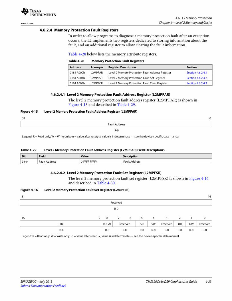
4.6 L2 Memory Protection
SPRUGW0C—July 2013 TMS320C66x DSP CorePac User Guide 4-33Submit Documentation Feedback
Chapter 4—Level 2 Memory and Cachewww.ti.com
4.6.2.4 Memory Protection Fault RegistersIn order to allow programs to diagnose a memory protection fault after an exception occurs, the L2 implements two registers dedicated to storing information about the fault, and an additional register to allow clearing the fault information.
Table 4-28 below lists the memory attribute registers.
4.6.2.4.1 Level 2 Memory Protection Fault Address Register (L2MPFAR) The level 2 memory protection fault address register (L2MPFAR) is shown in Figure 4-15 and described in Table 4-29.
4.6.2.4.2 Level 2 Memory Protection Fault Set Register (L2MPFSR)The level 2 memory protection fault set register (L2MPFSR) is shown in Figure 4-16 and described in Table 4-30.
Table 4-28 Memory Protection Fault Registers
Address Acronym Register Description Section
0184 A000h L2MPFAR Level 2 Memory Protection Fault Address Register Section 4.6.2.4.1
0184 A004h L2MPFSR Level 2 Memory Protection Fault Set Register Section 4.6.2.4.2
0184 A008h L2MPFCR Level 2 Memory Protection Fault Clear Register Section 4.6.2.4.3
Figure 4-15 Level 2 Memory Protection Fault Address Register (L2MPFAR)
31 0
Fault Address
R-0
Legend: R = Read only; W = Write only; -n = value after reset; -x, value is indeterminate — see the device-specific data manual
Table 4-29 Level 2 Memory Protection Fault Address Register (L2MPFAR) Field Descriptions
Bit Field Value Description
31-0 Fault Address 0-FFFF FFFFh Fault Address
Figure 4-16 Level 2 Memory Protection Fault Set Register (L2MPFSR)
31 16
Reserved
R-0
15 9 8 7 6 5 4 3 2 1 0
FID LOCAL Reserved SR SW Reserved UR UW Reserved
R-0 R-0 R-0 R-0 R-0 R-0 R-0 R-0 R-0
Legend: R = Read only; W = Write only; -n = value after reset; -x, value is indeterminate — see the device-specific data manual

4.6 L2 Memory Protection
4-34 TMS320C66x DSP CorePac User Guide SPRUGW0C—July 2013Submit Documentation Feedback
Chapter 4—Level 2 Memory and Cache www.ti.com
4.6.2.4.3 Level 2 Memory Protection Fault Clear Register (L2MPFCLR)The level 2 memory protection fault clear register (L2MPFCLR) is shown in Figure 4-17 and described in Table 4-31.
The memory access protection fault registers in Chapter 10 on page 10-1 defines the definition and meanings of these registers.
Table 4-30 Level 2 Memory Protection Fault Set Register (L2MPFSR) Field Descriptions
Bit Field Value Description
31-16 Reserved 0 Reserved
15-9 FID 0-7Fh Bit 6:0 of ID of faulting requestor. If ID is narrower than 7 bits, the remaining bits return 0. If ID is wider than 7 bits, the additional bits get truncated. FID = 0 if LOCAL = 1.
8 LOCAL 0 Normal operation.
1 Access was a "LOCAL" access
7-6 Reserved 0 Reserved
5 SR Supervisor read access type.
0 Normal operation.
1 Indicates a supervisor read request.
4 SW Supervisor write access type.
0 Normal operation.
1 Indicates a supervisor write request.
3 Reserved 0 Reserved
2 UR User read access type.
0 Normal operation.
1 Indicates a user read request.
1 UW User write access type.
0 Normal operation.
1 Indicates a user write request.
0 Reserved 0 Reserved
Figure 4-17 Level 2 Memory Protection Fault Clear Register (L2MPFCLR)
31 1 0
Reserved MPFCLR
R-0 W-0
Legend: R = Read only; W = Write only; -n = value after reset; -x, value is indeterminate — see the device-specific data manual
Table 4-31 Level 2 Memory Protection Fault Clear Register (L2MPFCLR) Field Descriptions
Bit Field Value Description
31-1 Reserved 0 Reserved
0 MPFCLR Command to clear the L2MPFCR register.
0 No effect.
1 Clear the L2MPFAR and the L2MPFCR registers.
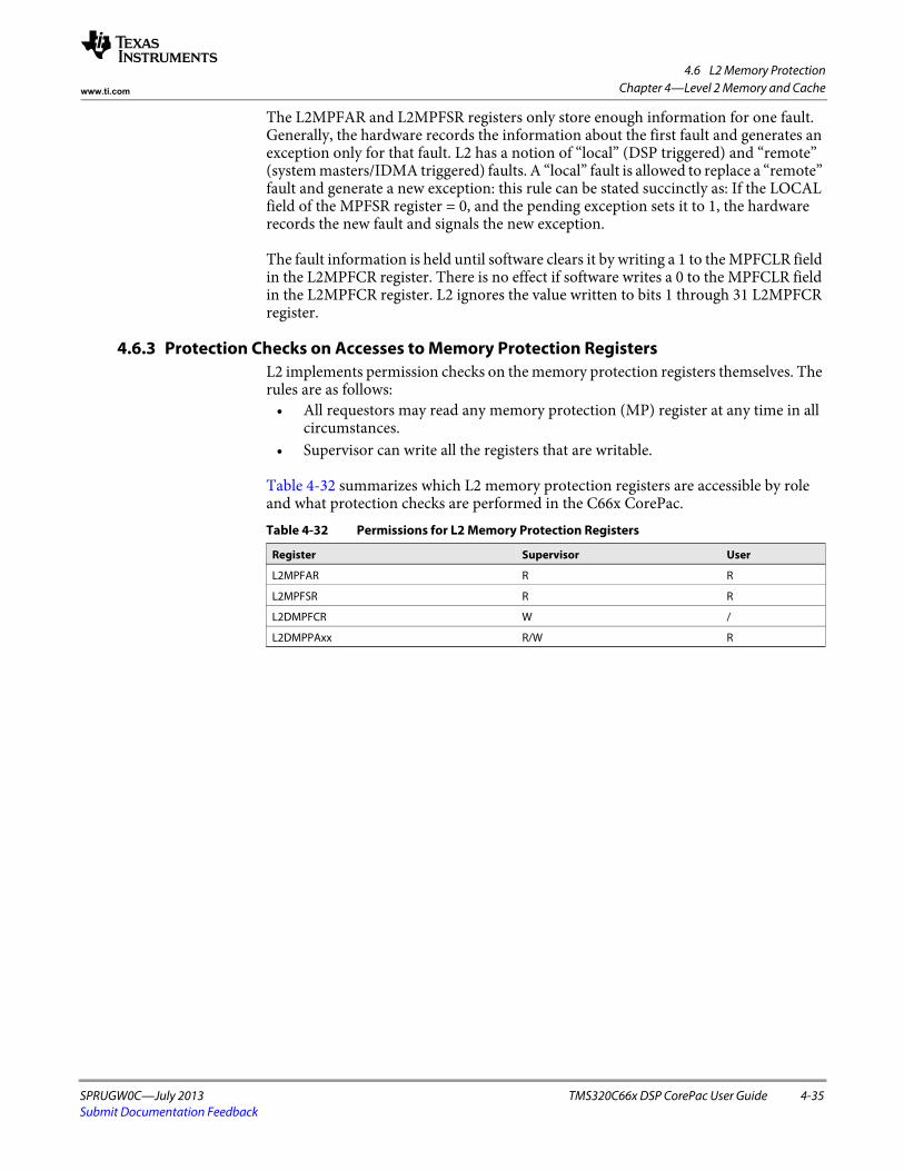
4.6 L2 Memory Protection
SPRUGW0C—July 2013 TMS320C66x DSP CorePac User Guide 4-35Submit Documentation Feedback
Chapter 4—Level 2 Memory and Cachewww.ti.com
The L2MPFAR and L2MPFSR registers only store enough information for one fault. Generally, the hardware records the information about the first fault and generates an exception only for that fault. L2 has a notion of “local” (DSP triggered) and “remote” (system masters/IDMA triggered) faults. A “local” fault is allowed to replace a “remote” fault and generate a new exception: this rule can be stated succinctly as: If the LOCAL field of the MPFSR register = 0, and the pending exception sets it to 1, the hardware records the new fault and signals the new exception.
The fault information is held until software clears it by writing a 1 to the MPFCLR field in the L2MPFCR register. There is no effect if software writes a 0 to the MPFCLR field in the L2MPFCR register. L2 ignores the value written to bits 1 through 31 L2MPFCR register.
4.6.3 Protection Checks on Accesses to Memory Protection RegistersL2 implements permission checks on the memory protection registers themselves. The rules are as follows:
• All requestors may read any memory protection (MP) register at any time in all circumstances.
• Supervisor can write all the registers that are writable.
Table 4-32 summarizes which L2 memory protection registers are accessible by role and what protection checks are performed in the C66x CorePac.Table 4-32 Permissions for L2 Memory Protection Registers
Register Supervisor User
L2MPFAR R R
L2MPFSR R R
L2DMPFCR W /
L2DMPPAxx R/W R
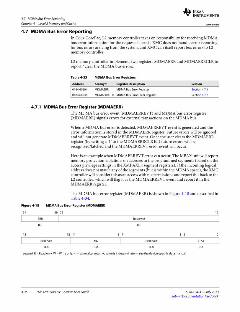
4.7 MDMA Bus Error Reporting
4-36 TMS320C66x DSP CorePac User Guide SPRUGW0C—July 2013Submit Documentation Feedback
Chapter 4—Level 2 Memory and Cache www.ti.com
4.7 MDMA Bus Error ReportingIn C66x CorePac, L2 memory controller takes on responsibility for receiving MDMA bus error information for the requests it sends. XMC does not handle error reporting for bus errors arriving from the system, and XMC can itself report bus errors to L2 memory controller.
L2 memory controller implements two registers MDMAERR and MDMAERRCLR to report / clear the MDMA bus errors.
4.7.1 MDMA Bus Error Register (MDMAERR)The MDMA bus error event (MDMAERREVT) and MDMA bus error register (MDMAERR) signals errors for external transactions on the MDMA bus.
When a MDMA bus error is detected, MDMAERREVT event is generated and the error information is stored in the MDMAERR register. Future errors will be ignored and will not generate MDMAERREVT event. Once the user clears the MDMAERR register (by writing a ‘1’ to the MDMAERRCLR bit) future errors will be recognized/latched and the MDMAERREVT error event will occur.
Here is an example when MDMAERREVT error can occur. The MPAX unit will report memory protection violations on accesses to the programmed segments (based on the access privilege settings in the XMPAXLn segment registers). If the incoming logical address does not match any of the segments (but is within the MDMA space), the XMC controller will consider this as an access with no permissions and report this back to the L2 controller, which will flag it as the MDMAERREVT event and report it in the MDMAERR register.
The MDMA bus error register (MDMAERR) is shown in Figure 4-18 and described in Table 4-34.
Table 4-33 MDMA Bus Error Registers
Address Acronym Register Description Section
0184 6020h MDMAERR MDMA Bus Error Register Section 4.7.1
0184 6024h MDMAERRCLR MDMA Bus Error Clear Register Section 4.7.2
Figure 4-18 MDMA Bus Error Register (MDMAERR)
31 29 28 16
ERR Reserved
R-0 R-0
15 12 11 8 7 3 2 0
Reserved XID Reserved STAT
R-0 R-0 R-0 R-0
Legend: R = Read only; W = Write only; -n = value after reset; -x, value is indeterminate — see the device-specific data manual
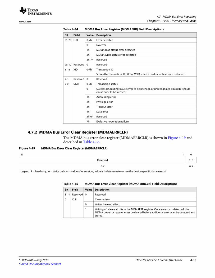
4.7 MDMA Bus Error Reporting
SPRUGW0C—July 2013 TMS320C66x DSP CorePac User Guide 4-37Submit Documentation Feedback
Chapter 4—Level 2 Memory and Cachewww.ti.com
4.7.2 MDMA Bus Error Clear Register (MDMAERRCLR)The MDMA bus error clear register (MDMAERRCLR) is shown in Figure 4-19 and described in Table 4-35.
Table 4-34 MDMA Bus Error Register (MDMAERR) Field Descriptions
Bit Field Value Description
31-29 ERR 0-7h Error detected
0 No error
1h MDMA read status error detected
2h MDMA write status error detected
3h-7h Reserved
28-12 Reserved 0 Reserved
11-8 XID 0-Fh Transaction ID
Stores the transaction ID (RID or WID) when a read or write error is detected.
7-3 Reserved 0 Reserved
2-0 STAT 0-7h Transaction status
0 Success (should not cause error to be latched), or unrecognized RID/WID (should cause error to be latched)
1h Addressing error
2h Privilege error
3h Timeout error
4h Data error
5h-6h Reserved
7h Exclusive - operation failure
Figure 4-19 MDMA Bus Error Clear Register (MDMAERRCLR)
31 1 0
Reserved CLR
R-0 W-0
Legend: R = Read only; W = Write only; -n = value after reset; -x, value is indeterminate — see the device-specific data manual
Table 4-35 MDMA Bus Error Clear Register (MDMAERRCLR) Field Descriptions
Bit Field Value Description
31-1 Reserved 0 Reserved
0 CLR Clear register
0 Writes have no effect
1 Writing a 1 clears all bits in the MDMAERR register. Once an error is detected, the MDMA bus error register must be cleared before additional errors can be detected and stored.
4.7 MDMA Bus Error Reporting
4-38 TMS320C66x DSP CorePac User Guide SPRUGW0C—July 2013Submit Documentation Feedback
Chapter 4—Level 2 Memory and Cache www.ti.com

SPRUGW0C—July 2013 TMS320C66x DSP CorePac User Guide 5-1Submit Documentation Feedback
Chapter 5
Internal Direct Memory Access (IDMA) Controller
5.1 "Introduction" on page 5-2 5.2 "Terms and Definitions" on page 5-3 5.3 "IDMA Architecture" on page 5-3 5.4 "IDMA Registers" on page 5-8 5.5 "Privilege Levels and IDMA Operation" on page 5-15
5.1 Introduction
5-2 TMS320C66x DSP CorePac User Guide SPRUGW0C—July 2013Submit Documentation Feedback
Chapter 5—Internal Direct Memory Access (IDMA) Controller www.ti.com
5.1 IntroductionThis section describes the purpose and features of the IDMA controller.
5.1.1 Purpose of the Internal Direct Memory Access (IDMA) ControllerThe purpose of the IDMA controller is to perform fast block transfers between any two memory locations local to the C66x CorePac. Local memory locations are defined as those in Level 1 program (L1P), Level 1 data (L1D), and Level 2 (L2) memories, or in the external peripheral configuration (CFG) memory. The IDMA cannot transfer data to or from the internal MMR space.
5.1.2 FeaturesThe IDMA controller allows rapid data transfers between all local memories. It provides a fast way to page code and data sections into any memory-mapped RAM local to the C66x CorePac. The key advantage of the IDMA controller is that it allows for transfers between slower (Level 2 - L2) and faster (Level 1 - L1D and L1P) memory. IDMA can provide lower latency than the cache controller since the transfers take place in the background of DSP operation, thereby removing stalls due to cache.
Additionally, the IDMA controller facilitates rapid programming of peripheral configuration registers accessed through the external configuration space (CFG) port of the C66x CorePac. The IDMA controller view of the external configuration space that has a 32-word granularity and allows any register within a 32-word block to be individually accessed.
In summary: • Optimized for burst transfers of memory blocks (contiguous data). • Allows access to and from any local memory (L1P, L1D, L2 (pages 0 and 1), and
external CFG (but, source and destination cannot both be in CFG). CFG is only accessible to channel 0. No CFG to CFG transfers.
• Indicates transfer completion through programmable interrupts to the DSP.
IDMA controller also provides the ability to do a block fill of memory, where the IDMA controller issues a block of writes using a fill value that you program.
5.2 Terms and Definitions
SPRUGW0C—July 2013 TMS320C66x DSP CorePac User Guide 5-3Submit Documentation Feedback
Chapter 5—Internal Direct Memory Access (IDMA) Controllerwww.ti.com
5.2 Terms and DefinitionsSee Appendix B on page B-1 of this document for a detailed definition of the terms used in this chapter. Appendix B on page B-1 describes general terms used throughout this reference guide.
5.3 IDMA ArchitectureThe IDMA controller allows both a means to rapidly transfer data between local memories and to rapidly program configuration registers. To fully support this, the IDMA controller consists of two channels, channel 0 and channel 1. The two channels are fully orthogonal to one another allowing concurrent operation.
The operation of the IDMA is controlled through several registers. Table 5-1 provides a summary of these registers. These registers are mentioned throughout this section and are described in more detail in Section 5.4.
5.3.1 IDMA Channel 0 IDMA channel 0 is intended for quick programming of configuration registers located in the external configuration space (CFG). It transfers data from a local memory (L1P, L1D, and L2) to the external configuration space.
The external configuration space includes the peripheral registers located outside of the C66x CorePac whereas the internal configuration space includes the registers located inside of the C66x CorePac. Any register described in this document belongs to the internal configuration space. For example, the registers that are used to control the level 1 data (L1D) cache are part of the internal configuration space. The internal configuration space is only accessible by the DSP using direct load/store instructions.
IDMA channel 0 can only access the external configuration space. It accesses blocks of 32 contiguous registers at a time. To implement this, IDMA channel 0 has five registers: status, mask, source address, destination address, and block count.
5.3.1.1 IDMA Channel 0 Operation The source and destination addresses that are used for IDMA channel 0 must be 32-byte aligned for proper operation. Figure 5-1 shows one possible transfer using IDMA channel 0.
Table 5-1 IDMA Register Description
Register Description
IDMA0_STAT IDMA0 Status Register
IDMA0_MASK IDMA0 Mask Register
IDMA0_SOURCE IDMA0 Source Address Register
IDMA0_DEST IDMA0 Destination Address Register
IDMA0_COUNT IDMA0 Block Count Register
IDMA1_STAT IDMA1 Status Register
IDMA1_SOURCE IDMA1 Source Address Register
IDMA1_DEST IDMA1 Destination Address Register
IDMA1_COUNT IDMA1 Block Count Register
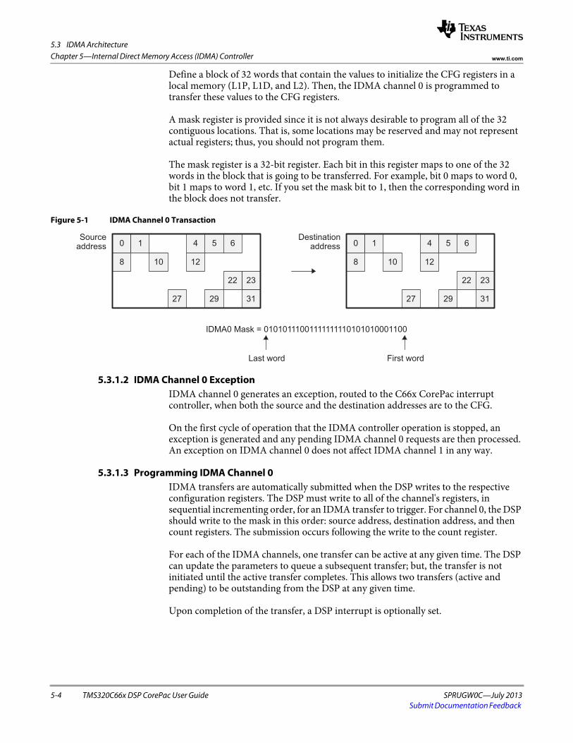
5.3 IDMA Architecture
5-4 TMS320C66x DSP CorePac User Guide SPRUGW0C—July 2013Submit Documentation Feedback
Chapter 5—Internal Direct Memory Access (IDMA) Controller www.ti.com
Define a block of 32 words that contain the values to initialize the CFG registers in a local memory (L1P, L1D, and L2). Then, the IDMA channel 0 is programmed to transfer these values to the CFG registers.
A mask register is provided since it is not always desirable to program all of the 32 contiguous locations. That is, some locations may be reserved and may not represent actual registers; thus, you should not program them.
The mask register is a 32-bit register. Each bit in this register maps to one of the 32 words in the block that is going to be transferred. For example, bit 0 maps to word 0, bit 1 maps to word 1, etc. If you set the mask bit to 1, then the corresponding word in the block does not transfer.
Figure 5-1 IDMA Channel 0 Transaction
5.3.1.2 IDMA Channel 0 ExceptionIDMA channel 0 generates an exception, routed to the C66x CorePac interrupt controller, when both the source and the destination addresses are to the CFG.
On the first cycle of operation that the IDMA controller operation is stopped, an exception is generated and any pending IDMA channel 0 requests are then processed. An exception on IDMA channel 0 does not affect IDMA channel 1 in any way.
5.3.1.3 Programming IDMA Channel 0 IDMA transfers are automatically submitted when the DSP writes to the respective configuration registers. The DSP must write to all of the channel's registers, in sequential incrementing order, for an IDMA transfer to trigger. For channel 0, the DSP should write to the mask in this order: source address, destination address, and then count registers. The submission occurs following the write to the count register.
For each of the IDMA channels, one transfer can be active at any given time. The DSP can update the parameters to queue a subsequent transfer; but, the transfer is not initiated until the active transfer completes. This allows two transfers (active and pending) to be outstanding from the DSP at any given time.
Upon completion of the transfer, a DSP interrupt is optionally set.
0 1
8 10
54 6
12
2322
29 3127
Sourceaddress
22
address 6540 1
8
27 29
1210
Destination
31
23
IDMA0 Mask = 01010111001111111110101010001100
Last word First word

5.3 IDMA Architecture
SPRUGW0C—July 2013 TMS320C66x DSP CorePac User Guide 5-5Submit Documentation Feedback
Chapter 5—Internal Direct Memory Access (IDMA) Controllerwww.ti.com
5.3.1.3.1 IDMA Channel 0 Example 1An example of making an update to configuration registers using IDMA channel 0 is shown in the following pseudo-code in Example 5-1.Example 5-1 Update to Configuration Registers using IDMA Channel 0
IDMA0_MASK = 0x00000F0F; //Set mask for 8 regs -- 11:8, 3:0IDMA0_SOURCE = MMR_ADDRESS; //Set source to config locationIDMA0_DEST = reg_ptr; //Set destination to data memory addressIDMA0_COUNT = 0; //Set mask for 1 block
while (IDMA0_STATUS); //Wait for transfer completion
... update register values ... IDMA0_MASK = 0x00000F0F; //Set mask for 8 regs -- 11:8, 3:0IDMA0_SOURCE = reg_ptr; //Set source to updated value pointer IDMA0_DEST = MMR_ADDRESS; //Set destination to config location IDMA0_COUNT = 0; //Set mask for 1 block
End of Example 5-1
5.3.1.3.2 IDMA Channel 0 Example 2EDMA is a peripheral commonly available on C66x devices. An example of submitting multiple QDMA requests is illustrated in Example 5-2. There are sixteen 8-word locations in configuration space within the EDMA that can correspond to the QDMA. Each QDMA submits a transfer request, as defined by an 8-word parameter entry.
Example 5-2 shows how 32 QDMAs can be issued, modifying only the source address, destination address, and options for each QDMA, as is possible in a video application.
See the EDMA documentation for more information about the QDMA.
Example 5-2 Update to 32 QDMAs using IDMA Channel 0
IDMA0_MASK = 0x4F4F4F4F;//Set mask for 0, 1, 2, 3, 6 for each QDMA IDMA0_SOURCE = &qdma_list[0]; //Set source to transfer listIDMA0_DEST = &QDMA[0]; //Set destination to base address of QDMAsIDMA0_COUNT = 3; //Set mask for 4 blocks (16 QDMAs)
IDMA0_MASK = 0x4F4F4F4F; //Set mask for 0, 1, 2, 3, 6 for each QDMAIDMA0_SOURCE = &qdma_list[16]; //Set source to second half of transfer listIDMA0_DEST = &QDMA[0]; //Set destination to base address of QDMAsIDMA0_COUNT = 3; //Set mask for 4 blocks (16 QDMAs)
while (IDMA0_STATUS); //Wait for transfer completion
End of Example 5-2
5.3.2 IDMA Channel 1IDMA channel 1 is intended for transferring data between local memories. It moves data and program sections in the background without DSP operation to set up processing from fast memory. To allow this, IDMA channel 1 has four registers: status, source address, destination address, and count.
5.3.2.1 IDMA Channel 1 Operation All source and destination addresses increment linearly throughout the transfer. The size (in bytes) of the transfer is set by the COUNT field in the IDMA channel 1 count register (IDMA1_COUNT). Following the transfer, a DSP interrupt is optionally set. Arbitration during any conflicts with the cache or EDMA is based on the priority set in
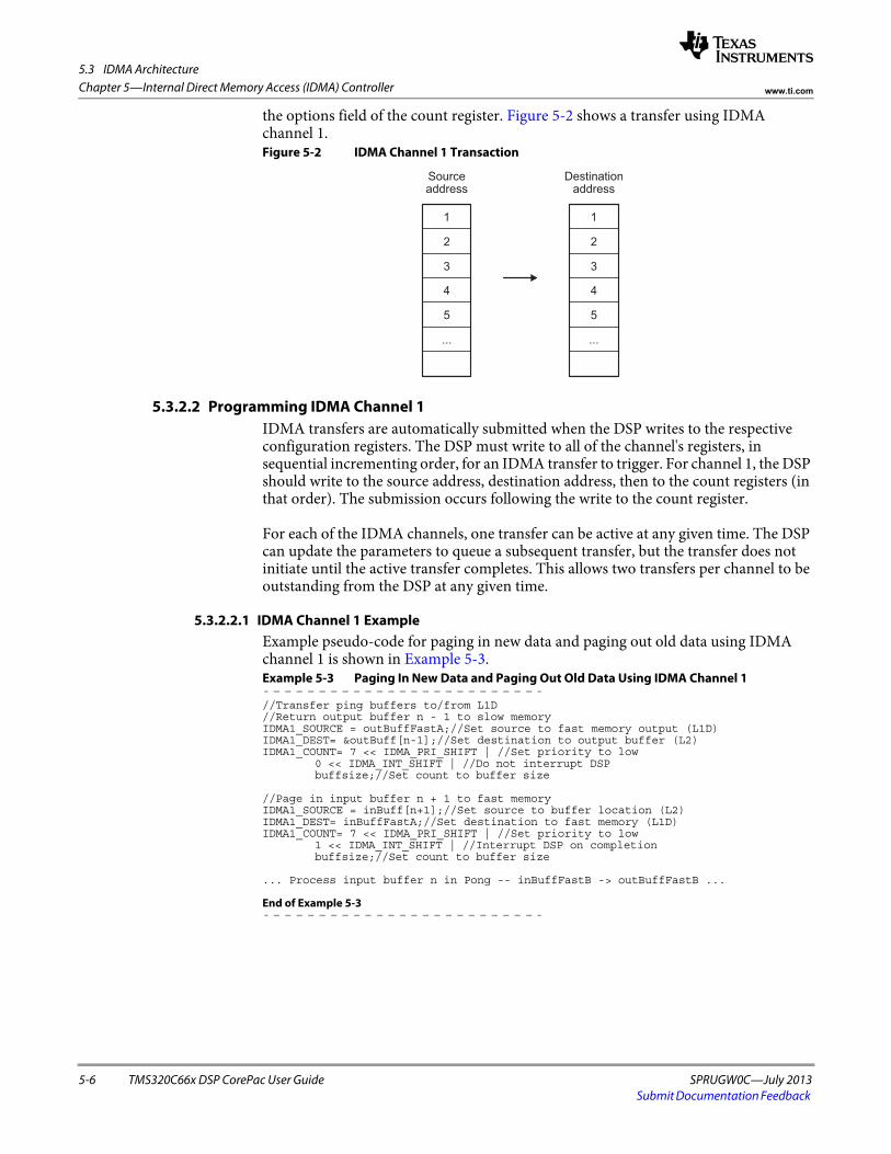
5.3 IDMA Architecture
5-6 TMS320C66x DSP CorePac User Guide SPRUGW0C—July 2013Submit Documentation Feedback
Chapter 5—Internal Direct Memory Access (IDMA) Controller www.ti.com
the options field of the count register. Figure 5-2 shows a transfer using IDMA channel 1.Figure 5-2 IDMA Channel 1 Transaction
5.3.2.2 Programming IDMA Channel 1IDMA transfers are automatically submitted when the DSP writes to the respective configuration registers. The DSP must write to all of the channel's registers, in sequential incrementing order, for an IDMA transfer to trigger. For channel 1, the DSP should write to the source address, destination address, then to the count registers (in that order). The submission occurs following the write to the count register.
For each of the IDMA channels, one transfer can be active at any given time. The DSP can update the parameters to queue a subsequent transfer, but the transfer does not initiate until the active transfer completes. This allows two transfers per channel to be outstanding from the DSP at any given time.
5.3.2.2.1 IDMA Channel 1 Example Example pseudo-code for paging in new data and paging out old data using IDMA channel 1 is shown in Example 5-3. Example 5-3 Paging In New Data and Paging Out Old Data Using IDMA Channel 1
//Transfer ping buffers to/from L1D //Return output buffer n - 1 to slow memory IDMA1_SOURCE = outBuffFastA;//Set source to fast memory output (L1D)IDMA1_DEST= &outBuff[n-1];//Set destination to output buffer (L2)IDMA1_COUNT= 7 << IDMA_PRI_SHIFT | //Set priority to low
0 << IDMA_INT_SHIFT | //Do not interrupt DSPbuffsize;//Set count to buffer size
//Page in input buffer n + 1 to fast memoryIDMA1_SOURCE = inBuff[n+1];//Set source to buffer location (L2)IDMA1_DEST= inBuffFastA;//Set destination to fast memory (L1D)IDMA1_COUNT= 7 << IDMA_PRI_SHIFT | //Set priority to low
1 << IDMA_INT_SHIFT | //Interrupt DSP on completion buffsize;//Set count to buffer size
... Process input buffer n in Pong -- inBuffFastB -> outBuffFastB ...
End of Example 5-3
1
2
4
3
...
5
Sourceaddress
...
5
Destination
4
3
2
address
1
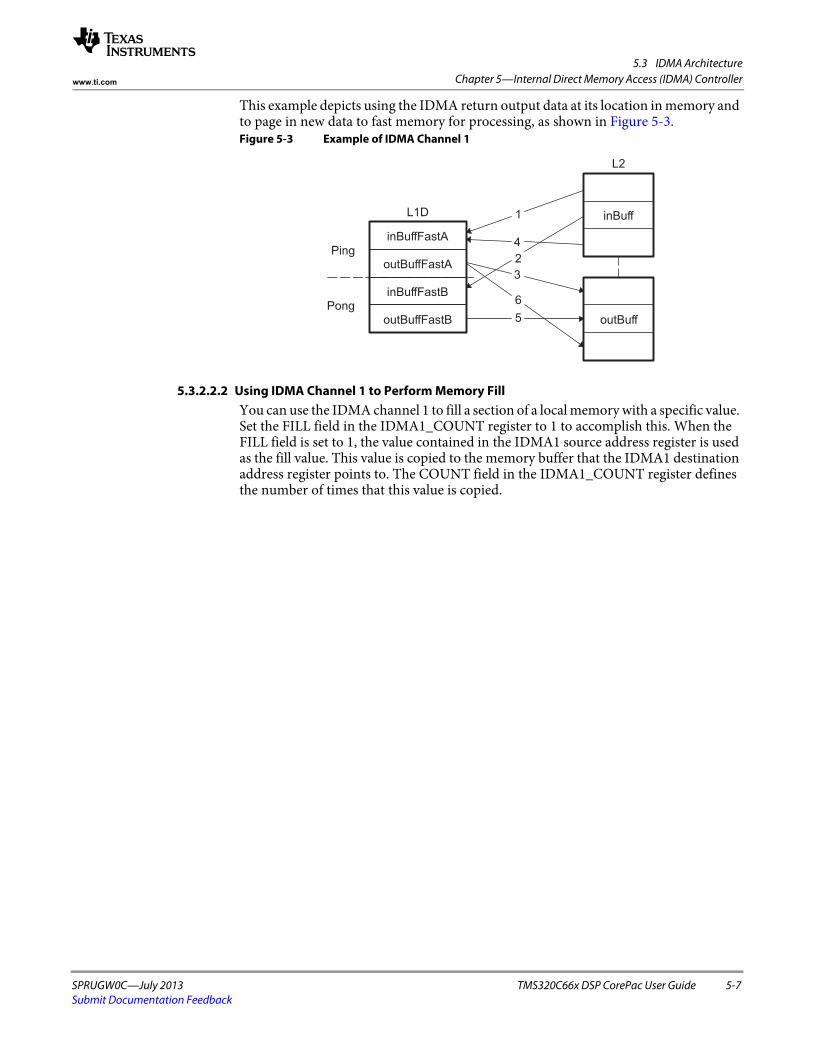
5.3 IDMA Architecture
SPRUGW0C—July 2013 TMS320C66x DSP CorePac User Guide 5-7Submit Documentation Feedback
Chapter 5—Internal Direct Memory Access (IDMA) Controllerwww.ti.com
This example depicts using the IDMA return output data at its location in memory and to page in new data to fast memory for processing, as shown in Figure 5-3. Figure 5-3 Example of IDMA Channel 1
5.3.2.2.2 Using IDMA Channel 1 to Perform Memory FillYou can use the IDMA channel 1 to fill a section of a local memory with a specific value. Set the FILL field in the IDMA1_COUNT register to 1 to accomplish this. When the FILL field is set to 1, the value contained in the IDMA1 source address register is used as the fill value. This value is copied to the memory buffer that the IDMA1 destination address register points to. The COUNT field in the IDMA1_COUNT register defines the number of times that this value is copied.
inBuffFastA
outBuffFastA
outBuffFastB
inBuffFastB
Ping
Pong
L1D inBuff
outBuff
L2
1
4
2
3
6
5

5.4 IDMA Registers
5-8 TMS320C66x DSP CorePac User Guide SPRUGW0C—July 2013Submit Documentation Feedback
Chapter 5—Internal Direct Memory Access (IDMA) Controller www.ti.com
5.4 IDMA RegistersThe IDMA controller is programmed through a set of registers, listed in Table 5-2. See the device-specific data manual for the memory address of these registers.
Each of the registers is accessible for read/write access by the DSP. Access to each of the IDMA registers must be 32-bit aligned. Half word and byte writes to the IDMA registers write the entire register, and thus you should avoid them for proper operation. Nonaligned word and double word accesses result in unpredictable operation, and so you should avoid them as well.
Table 5-1 lists all of the registers in the IDMA.
5.4.1 IDMA Channel 0 Status Register (IDMA0_STAT)The IDMA channel 0 status register (IDMA0_STAT) provides the activity state of the channel. There are two bits to denote whether a transfer is in progress (ACTV) and whether a transfer is pending (PEND). The IDMA channel 0 status register (IDMA0_STAT) is shown in Figure 5-4 and described in Table 5-3.
Table 5-2 Internal Direct Memory Access (IDMA) Registers
Address Acronym Register Description Section
0182 0000h IDMA0_STAT IDMA Channel 0 Status Register Section 5.4.1
0182 0004h IDMA0_MASK IDMA Channel 0 Mask Register Section 5.4.2
0182 0008h IDMA0_SOURCE IDMA Channel 0 Source Address Register Section 5.4.3
0182 000Ch IDMA0_DEST IDMA Channel 0 Destination Address Register Section 5.4.4
0182 0010h IDMA0_COUNT IDMA Channel 0 Block Count Register Section 5.4.5
0182 0100h IDMA1_STAT IDMA Channel 1 Status Register Section 5.4.6
0182 0108h IDMA1_SOURCE IDMA Channel 1 Source Address Register Section 5.4.7
0182 010Ch IDMA1_DEST IDMA Channel 1 Destination Address Register Section 5.4.8
0182 0110h IDMA1_COUNT IDMA Channel 1 Block Count Register Section 5.4.9
Figure 5-4 IDMA Channel 0 Status Register (IDMA0_STAT)
31 16
Reserved
R-0
15 2 1 0
Reserved PEND ACTV
R-0 R-0 R-0
Legend: R = Read only; W = Write only; -n = value after reset; -x, value is indeterminate — see the device-specific data manual

5.4 IDMA Registers
SPRUGW0C—July 2013 TMS320C66x DSP CorePac User Guide 5-9Submit Documentation Feedback
Chapter 5—Internal Direct Memory Access (IDMA) Controllerwww.ti.com
5.4.2 IDMA Channel 0 Mask Register (IDMA0_MASK)The IDMA channel 0 mask register (IDMA0_MASK) allows unwanted registers within the transfer block to be masked. There are 32 bits that allow individual control over the registers within the 32-word memory block identified by the source/destination address registers.
The IDMA channel 0 mask register (IDMA0_MASK) is shown in Figure 5-5 and described in Table 5-4.
5.4.3 IDMA Channel 0 Source Address Register (IDMA0_SOURCE)The IDMA channel 0 source address register (IDMA0_SOURCE) identifies the source address for the IDMA transfer. The source of the transfer must be local to the C66x CorePac, either in L1P, L1D, L2, or CFG. The source address for the transfer must be a local RAM location, if the destination address is to CFG. Conversely, the source address must be to CFG, if the destination address is to a local RAM location. Additionally, the source address must be 32-byte aligned.
Table 5-3 IDMA Channel 0 Status Register (IDMA0_STAT) Field Descriptions
Bit Field Value Description
31-2 Reserved 0 These reserved bit locations are always read as zeros. A value written to this field has no effect.
1 PEND Pending transfer. The PEND bit sets when the DSP writes control registers and an active transfer is already in progress (ACTV = 1). The PEND bit clears when the transfer becomes active.
0 No pending transfer
1 Transfer is pending
0 ACTV Active transfer. The ACTV bit sets when channel 0 begins reading data from the source address register (IDMA0_SOURCE) and clears following the last write to the destination address register (IDMA0_DEST).
0 No active transfer
1 Active transfer
Figure 5-5 IDMA Channel 0 Mask Register (IDMA0_MASK)
31 30 29 28 27 26 25 24 23 22 21 20 19 18 17 16
M31 M30 M29 M28 M27 M26 M25 M24 M23 M22 M21 M20 M19 M18 M17 M16
R/W-0 R/W-0 R/W-0 R/W-0 R/W-0 R/W-0 R/W-0 R/W-0 R/W-0 R/W-0 R/W-0 R/W-0 R/W-0 R/W-0 R/W-0 R/W-0
15 14 13 12 11 10 9 8 7 6 5 4 3 2 1 0
M15 M14 M13 M12 M11 M10 M9 M8 M7 M6 M5 M4 M3 M2 M1 M0
R/W-0 R/W-0 R/W-0 R/W-0 R/W-0 R/W-0 R/W-0 R/W-0 R/W-0 R/W-0 R/W-0 R/W-0 R/W-0 R/W-0 R/W-0 R/W-0
Legend: R = Read only; W = Write only; -n = value after reset; -x, value is indeterminate — see the device-specific data manual
Table 5-4 IDMA Channel 0 Mask Register (IDMA0_MASK) Field Descriptions
Bit Field Value Description
31-0 Mn Register mask bit.
0 Register access permitted (not masked).
1 Register access blocked (masked).
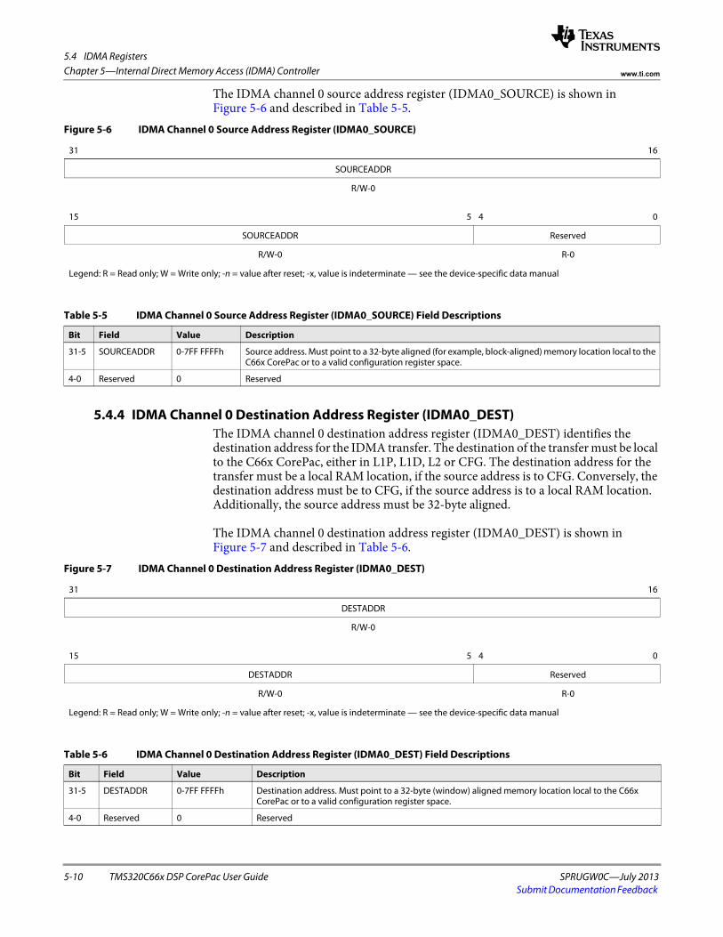
5.4 IDMA Registers
5-10 TMS320C66x DSP CorePac User Guide SPRUGW0C—July 2013Submit Documentation Feedback
Chapter 5—Internal Direct Memory Access (IDMA) Controller www.ti.com
The IDMA channel 0 source address register (IDMA0_SOURCE) is shown in Figure 5-6 and described in Table 5-5.
5.4.4 IDMA Channel 0 Destination Address Register (IDMA0_DEST)The IDMA channel 0 destination address register (IDMA0_DEST) identifies the destination address for the IDMA transfer. The destination of the transfer must be local to the C66x CorePac, either in L1P, L1D, L2 or CFG. The destination address for the transfer must be a local RAM location, if the source address is to CFG. Conversely, the destination address must be to CFG, if the source address is to a local RAM location. Additionally, the source address must be 32-byte aligned.
The IDMA channel 0 destination address register (IDMA0_DEST) is shown in Figure 5-7 and described in Table 5-6.
Figure 5-6 IDMA Channel 0 Source Address Register (IDMA0_SOURCE)
31 16
SOURCEADDR
R/W-0
15 5 4 0
SOURCEADDR Reserved
R/W-0 R-0
Legend: R = Read only; W = Write only; -n = value after reset; -x, value is indeterminate — see the device-specific data manual
Table 5-5 IDMA Channel 0 Source Address Register (IDMA0_SOURCE) Field Descriptions
Bit Field Value Description
31-5 SOURCEADDR 0-7FF FFFFh Source address. Must point to a 32-byte aligned (for example, block-aligned) memory location local to the C66x CorePac or to a valid configuration register space.
4-0 Reserved 0 Reserved
Figure 5-7 IDMA Channel 0 Destination Address Register (IDMA0_DEST)
31 16
DESTADDR
R/W-0
15 5 4 0
DESTADDR Reserved
R/W-0 R-0
Legend: R = Read only; W = Write only; -n = value after reset; -x, value is indeterminate — see the device-specific data manual
Table 5-6 IDMA Channel 0 Destination Address Register (IDMA0_DEST) Field Descriptions
Bit Field Value Description
31-5 DESTADDR 0-7FF FFFFh Destination address. Must point to a 32-byte (window) aligned memory location local to the C66x CorePac or to a valid configuration register space.
4-0 Reserved 0 Reserved
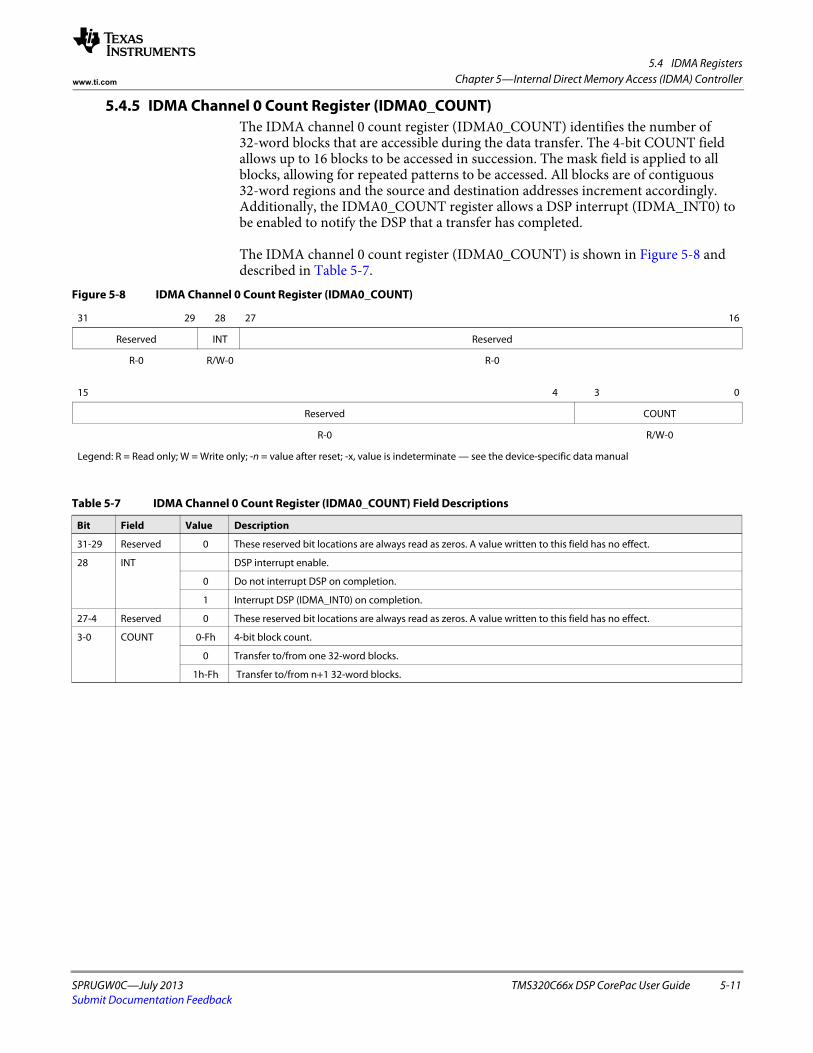
5.4 IDMA Registers
SPRUGW0C—July 2013 TMS320C66x DSP CorePac User Guide 5-11Submit Documentation Feedback
Chapter 5—Internal Direct Memory Access (IDMA) Controllerwww.ti.com
5.4.5 IDMA Channel 0 Count Register (IDMA0_COUNT)The IDMA channel 0 count register (IDMA0_COUNT) identifies the number of 32-word blocks that are accessible during the data transfer. The 4-bit COUNT field allows up to 16 blocks to be accessed in succession. The mask field is applied to all blocks, allowing for repeated patterns to be accessed. All blocks are of contiguous 32-word regions and the source and destination addresses increment accordingly. Additionally, the IDMA0_COUNT register allows a DSP interrupt (IDMA_INT0) to be enabled to notify the DSP that a transfer has completed.
The IDMA channel 0 count register (IDMA0_COUNT) is shown in Figure 5-8 and described in Table 5-7.
Figure 5-8 IDMA Channel 0 Count Register (IDMA0_COUNT)
31 29 28 27 16
Reserved INT Reserved
R-0 R/W-0 R-0
15 4 3 0
Reserved COUNT
R-0 R/W-0
Legend: R = Read only; W = Write only; -n = value after reset; -x, value is indeterminate — see the device-specific data manual
Table 5-7 IDMA Channel 0 Count Register (IDMA0_COUNT) Field Descriptions
Bit Field Value Description
31-29 Reserved 0 These reserved bit locations are always read as zeros. A value written to this field has no effect.
28 INT DSP interrupt enable.
0 Do not interrupt DSP on completion.
1 Interrupt DSP (IDMA_INT0) on completion.
27-4 Reserved 0 These reserved bit locations are always read as zeros. A value written to this field has no effect.
3-0 COUNT 0-Fh 4-bit block count.
0 Transfer to/from one 32-word blocks.
1h-Fh Transfer to/from n+1 32-word blocks.
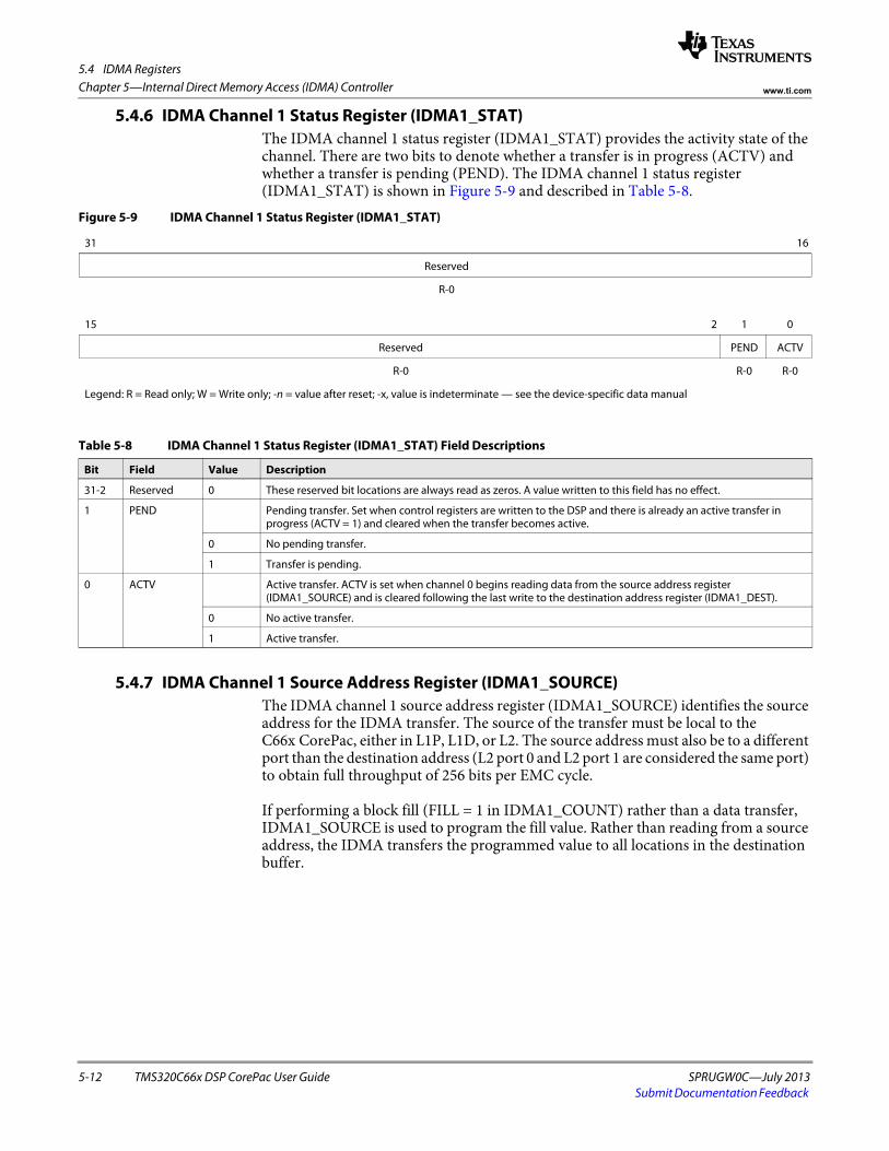
5.4 IDMA Registers
5-12 TMS320C66x DSP CorePac User Guide SPRUGW0C—July 2013Submit Documentation Feedback
Chapter 5—Internal Direct Memory Access (IDMA) Controller www.ti.com
5.4.6 IDMA Channel 1 Status Register (IDMA1_STAT)The IDMA channel 1 status register (IDMA1_STAT) provides the activity state of the channel. There are two bits to denote whether a transfer is in progress (ACTV) and whether a transfer is pending (PEND). The IDMA channel 1 status register (IDMA1_STAT) is shown in Figure 5-9 and described in Table 5-8.
5.4.7 IDMA Channel 1 Source Address Register (IDMA1_SOURCE)The IDMA channel 1 source address register (IDMA1_SOURCE) identifies the source address for the IDMA transfer. The source of the transfer must be local to the C66x CorePac, either in L1P, L1D, or L2. The source address must also be to a different port than the destination address (L2 port 0 and L2 port 1 are considered the same port) to obtain full throughput of 256 bits per EMC cycle.
If performing a block fill (FILL = 1 in IDMA1_COUNT) rather than a data transfer, IDMA1_SOURCE is used to program the fill value. Rather than reading from a source address, the IDMA transfers the programmed value to all locations in the destination buffer.
Figure 5-9 IDMA Channel 1 Status Register (IDMA1_STAT)
31 16
Reserved
R-0
15 2 1 0
Reserved PEND ACTV
R-0 R-0 R-0
Legend: R = Read only; W = Write only; -n = value after reset; -x, value is indeterminate — see the device-specific data manual
Table 5-8 IDMA Channel 1 Status Register (IDMA1_STAT) Field Descriptions
Bit Field Value Description
31-2 Reserved 0 These reserved bit locations are always read as zeros. A value written to this field has no effect.
1 PEND Pending transfer. Set when control registers are written to the DSP and there is already an active transfer in progress (ACTV = 1) and cleared when the transfer becomes active.
0 No pending transfer.
1 Transfer is pending.
0 ACTV Active transfer. ACTV is set when channel 0 begins reading data from the source address register (IDMA1_SOURCE) and is cleared following the last write to the destination address register (IDMA1_DEST).
0 No active transfer.
1 Active transfer.

5.4 IDMA Registers
SPRUGW0C—July 2013 TMS320C66x DSP CorePac User Guide 5-13Submit Documentation Feedback
Chapter 5—Internal Direct Memory Access (IDMA) Controllerwww.ti.com
The IDMA channel 1 source address register (IDMA1_SOURCE) is shown in Figure 5-10 and described in Table 5-9.
5.4.8 IDMA Channel 1 Destination Address Register (IDMA1_DEST)The IDMA channel 1 destination address register (IDMA1_DEST) identifies the destination address for the IDMA transfer. The destination of the transfer must be local to the C66x CorePac, either in L1P, L1D, or L2. The destination address must also be to a different port than the source address (L2 port 0 and L2 port 1 are considered the same port) to obtain full throughput of 256 bits per EMC cycle.
The IDMA channel 1 destination address register (IDMA1_DEST) is shown in Figure 5-11 and described in Table 5-10.
Figure 5-10 IDMA Channel 1 Source Address Register (IDMA1_SOURCE)
31 16
SOURCEADDR
R/W-0
15 0
SOURCEADDR
R/W-0
Legend: R = Read only; W = Write only; -n = value after reset; -x, value is indeterminate — see the device-specific data manual
Table 5-9 IDMA Channel 1 Source Address Register (IDMA1_SOURCE) Field Descriptions
Bit Field Value Description
31-0 SOURCEADDR 0-FFFF FFFFh Source address. Must point to a word-aligned memory location local to the C66x CorePac. When performing a block fill (FILL = 1 in IDMA1_COUNT), the source address is the fill value. Note that when performing a fill mode transfer, all 32-bits of the SOURCEADDR field are used when performing a memory transfer, the two LSBs are implemented as 00b.
Figure 5-11 IDMA Channel 1 Destination Address Register (IDMA1_DEST)
31 16
DESTADDR
R/W-0
15 2 1 0
DESTADDR Reserved
R/W-0 R-0
Legend: R = Read only; W = Write only; -n = value after reset; -x, value is indeterminate — see the device-specific data manual
Table 5-10 IDMA Channel 1 Destination Address Register (IDMA1_DEST) Field Descriptions
Bit Field Value Description
31-2 DESTADDR 0-3FFF FFFFh Destination address. Must point to a word-aligned memory location local to the C66x CorePac
1-0 Reserved 0 Reserved

5.4 IDMA Registers
5-14 TMS320C66x DSP CorePac User Guide SPRUGW0C—July 2013Submit Documentation Feedback
Chapter 5—Internal Direct Memory Access (IDMA) Controller www.ti.com
5.4.9 IDMA Channel 1 Count Register (IDMA1_COUNT)The IDMA channel 1 count register (IDMA1_COUNT) identifies the transfer length in bytes. In addition, IDMA1_COUNT allows a DSP interrupt (IDMA_INT1) to be enabled and identifies the priority level (relative to DSP and other DMA accesses) to be specified.
The IDMA channel 1 count register (IDMA1_COUNT) is shown in Figure 5-12 5 and described in Table 5-11.
A transfer count of zero is a possible programming option. The IDMA engine handles a count of zero by “completing” the transfer immediately (i.e., if the INT bit in the IDMA1_COUNT register asserts IDMA_INT1 to the DSP even though no data actually transfers). If a subsequent transfer is pending, it begins immediately.
Figure 5-12 IDMA Channel 1 Count Register (IDMA1_COUNT)
31 29 28 27 17 16
PRI INT Reserved FILL
R/W-0 R/W-0 R-0 R/W-0
15 0
COUNT
R/W-0
Legend: R = Read only; W = Write only; -n = value after reset; -x, value is indeterminate — see the device-specific data manual
Table 5-11 IDMA Channel 1 Count Register (IDMA1_COUNT) Field Descriptions
Bit Field Value Description
31-29 PRI 0-7h Transfer priority. Used for arbitration between DSP and DMA accesses when there are conflicts. Note that priority can be any value between 0 (highest priority) and 7 (lowest priority).
28 INT DSP interrupt enable.
0 Do not interrupt DSP on completion.
1 Interrupt DSP (IDMA_INT1) on completion.
27-17 Reserved 0 These reserved bit locations are always read as zeros. A value written to this field has no effect.
16 FILL Block fill
0 Block transfer from the source address register (IDMA1_SOURCE) to the destination address register (IDMA1_DEST).
1 Perform a block fill using the source address register (IDMA1_SOURCE) as the fill value to the memory buffer pointed to by the destination address register (IDMA1_DEST).
15-0 COUNT 0-FFh Byte count. A 16-bit count that defines the transfer length in bytes. Must be a multiple of 4 bytes. A transfer count of zero will not transfer any data, but generates an interrupt if requested by the INT bit. For correct operation, the two ISBs must always be 0.

5.5 Privilege Levels and IDMA Operation
SPRUGW0C—July 2013 TMS320C66x DSP CorePac User Guide 5-15Submit Documentation Feedback
Chapter 5—Internal Direct Memory Access (IDMA) Controllerwww.ti.com
5.5 Privilege Levels and IDMA OperationTable 5-12 summarizes which IDMA registers are accessible and what protection checks are performed in the C66x CorePac based on role.Table 5-12 Permissions for IDMA Registers
Register Supervisor User
IDMA0_STAT R R
IDMA0_MASK R/W R/W
IDMA0_SOURCE R/W R/W
IDMA0_DEST R/W R/W
IDMA0_COUNT R/W R/W
IDMA1_STAT R R
IDMA1_SOURCE R/W R/W
IDMA1_DEST R/W R/W
IDMA1_COUNT R/W R/W
5.5 Privilege Levels and IDMA Operation
5-16 TMS320C66x DSP CorePac User Guide SPRUGW0C—July 2013Submit Documentation Feedback
Chapter 5—Internal Direct Memory Access (IDMA) Controller www.ti.com
SPRUGW0C—July 2013 TMS320C66x DSP CorePac User Guide 6-1Submit Documentation Feedback
Chapter 6
External Memory Controller (EMC)
6.1 "Introduction" on page 6-2 6.2 "PrivID to AID Remap Table" on page 6-2 6.3 "PrivID to AID Mapping" on page 6-3 6.4 "CFG Bus Error Reporting" on page 6-3

6.1 Introduction
6-2 TMS320C66x DSP CorePac User Guide SPRUGW0C—July 2013Submit Documentation Feedback
Chapter 6—External Memory Controller (EMC) www.ti.com
6.1 IntroductionThe external memory controller (EMC) is a bridge from the CorePac to the rest of the device. It includes two ports:
• Configuration registers (CFG)—This port provides access to the memory-mapped registers which control various peripherals and resources on C66x devices.
Note—This port does not provide access to those control registers found within the DSP or the CorePac.
• Slave DMA (SDMA)—The slave DMA provides access to resources inside the C66x CorePac to system masters found outside the C66x CorePac such as DMA controllers, SRIO, etc. That is, transfers initiated outside the C66x CorePac where the C66x CorePac is the slave in the transaction.
6.2 PrivID to AID Remap TableThe EMC remaps PrivIDs on inbound accesses to the smaller set of AIDs that C66x CorePac recognizes. EMC contains a small 16 entry by three-bit table, exposed to the programmer as the following table of PrivID to AID Mapping (PAMAP) registers.Table 6-1 PrivID to AID Mapping (PAMAP) Registers)
31 3 2 0
PAMAP0 Reserved AID 0182_0500
PAMAP1 Reserved AID 0182_0504
PAMAP2 Reserved AID 0182_0508
PAMAP3 Reserved AID 0182_050C
PAMAP4 Reserved AID 0182_0510
PAMAP5 Reserved AID 0182_0514
PAMAP6 Reserved AID 0182_0518
PAMAP7 Reserved AID 0182_051C
PAMAP8 Reserved AID 0182_0520
PAMAP9 Reserved AID 0182_0524
PAMAP10 Reserved AID 0182_0528
PAMAP11 Reserved AID 0182_052C
PAMAP12 Reserved AID 0182_0530
PAMAP13 Reserved AID 0182_0534
PAMAP14 Reserved AID 0182_0538
PAMAP15 Reserved AID 0182_053C
R, +0 RW, +default

6.3 PrivID to AID Mapping
SPRUGW0C—July 2013 TMS320C66x DSP CorePac User Guide 6-3Submit Documentation Feedback
Chapter 6—External Memory Controller (EMC)www.ti.com
6.3 PrivID to AID MappingThe EMC remaps each incoming four-bit PrivID to a smaller three-bit ID space. The AID field in each PAMAP register is interpreted as follows:
Encodings 110b and 111b output ID numbers 6 and 7, respectively. The L1D memory controller, L1P memory controller, and L2 memory controller endpoints interpret both as AIDX in the C66x CorePac.
At power up, PAMAP0 through PAMAP7 contain the values 0 through 7, respectively. PAMAP8 through 15 all contain the value 7. This makes C66x CorePac behave identically to C64x+ for PrivIDs >= 6.
6.4 CFG Bus Error ReportingEMC handles error reporting for the configuration bus transactions. EMC implements two registers ECFGERR and ECFGERRCLR to report / clear the configuration bus errors.
6.4.1 CFG Bus Error Register (ECFGERR)The CFG bus error event (EMC_BUSERR) and the CFG bus error register (ECFGERR) signals error for transactions on the external configuration bus.
The CFG bus error register (ECFGERR) is shown in Figure 6-1 and described in Table 6-4.
Table 6-2 PrivID to AID Mapping Encoding
AID field Meaning
000 Map this PrivID to PrivID 0 / AID0 inside CorePac
001 Map this PrivID to PrivID 1 / AID1 inside CorePac
010 Map this PrivID to PrivID 2 / AID2 inside CorePac
011 Map this PrivID to PrivID 3 / AID3 inside CorePac
100 Map this PrivID to PrivID 4 / AID4 inside CorePac
101 Map this PrivID to PrivID 5 / AID5 inside CorePac
110 Map this PrivID to PrivID 6 / AIDX inside CorePac
111 Map this PrivID to PrivID 7 / AIDX inside CorePac
Table 6-3 CFG Bus Error Registers
Address Acronym Register Description Section
0182 0408h ECFGERR CFG Bus Error Register Section 6.4.1
0182 040Ch ECFGERRCLR CFG Bus Error Clear Register Section 6.4.2
Figure 6-1 CFG Bus Error Register (ECFGERR)
31 29 28 16
ERR Reserved
R-0 R-0
15 12 11 8 7 3 2 0
Reserved XID Reserved STAT
R-0 R-0 R-0 R-0
Legend: R = Read only; W = Write only; -n = value after reset; -x, value is indeterminate — see the device-specific data manual

6.4 CFG Bus Error Reporting
6-4 TMS320C66x DSP CorePac User Guide SPRUGW0C—July 2013Submit Documentation Feedback
Chapter 6—External Memory Controller (EMC) www.ti.com
6.4.2 CFG Bus Error Clear Register (ECFGERRCLR)The CFG bus error clear register (ECFGERRCLR) is shown in Figure 6-2 and described in Table 6-5.
Table 6-4 CFG Bus Error Register (ECFGERR) Field Descriptions
Bit Field Value Description
31-29 ERR 0-7h Error detected
0 No error
1h-2h Reserved
3h CFG read status error detected
4h CFG write status error detected
5h-7h Reserved
28-12 Reserved 0 Reserved
11-8 XID 0-Fh Transaction ID
Stores the transaction ID (RID or WID) when a read or write error is detected.
7-3 Reserved 0 Reserved
2-0 STAT 0-7h Transaction status
0 Success (should not cause error to be latched), or unrecognized RID/WID (should cause error to be latched)
1h Addressing error
2h Privilege error
3h Timeout error
4h Data error
5h-6h Reserved
7h Exclusive - operation failure
Figure 6-2 CFG Bus Error Clear Register (ECFGERRCLR)
31 16
Reserved
R-0
15 1 0
Reserved CLR
R-0 W-0
Legend: R = Read only; W = Write only; -n = value after reset; -x, value is indeterminate — see the device-specific data manual
Table 6-5 CFG Bus Error Clear Register (ECFGERRCLR) Field Descriptions
Bit Field Value Description
31-1 Reserved 0 Reserved
0 CLR Clear register
0 Writes have no effect
1 Writing a 1 clears all bits in the ECFGERR register. Once an error is detected, the CFG bus error register must be cleared before additional errors can be detected and stored.

SPRUGW0C—July 2013 TMS320C66x DSP CorePac User Guide 7-1Submit Documentation Feedback
Chapter 7
Extended Memory Controller (XMC)
7.1 "Introduction" on page 7-2 7.2 "Memory Mapped Register Summary" on page 7-2 7.3 "XMC Memory Protection and Address eXtension (MPAX)" on page 7-5 7.4 "XMC Memory Protection Architecture Support" on page 7-13 7.5 "Prefetch Buffers" on page 7-14 7.6 "Prefetch Buffer Memory Mapped Registers" on page 7-17

7.1 Introduction
7-2 TMS320C66x DSP CorePac User Guide SPRUGW0C—July 2013Submit Documentation Feedback
Chapter 7—Extended Memory Controller (XMC) www.ti.com
7.1 IntroductionThe Extended Memory Controller (XMC) serves as the L2 memory controller’s MDMA path to the MSMC. XMC has three additional responsibilities: Memory protection, Address extension, and Prefetch.
The XMC performs the roles listed below:• Shared memory access path• Memory protection for addresses outside C66x CorePac—for example, MSMC,
RAM, or EMIF • Address extension/translation • Prefetch support
Memory protection and address extension are provided together in a unit called MPAX. The MPAX defines 16 segments of runtime-selectable size that project C66x CorePac’s 32-bit address space into a larger 36-bit address space. In addition, each segment has a corresponding set of permissions to control accesses to that segment. The two together provide a convenient mechanism for multiple DSPs to cooperate in a large shared memory. The memory protection scheme is also designed to coordinate with other memory protection units and firewalls that may be in the system.
Prefetch support in XMC aims to reduce the read miss penalty for streams of data entering C66x CorePac. Hence prefetching helps to reduce stall cycles and thereby improves memory read performance to MSMC RAM and EMIF.
7.2 Memory Mapped Register SummaryThe XMC does not provide a separate configuration interface for its memory mapped registers. Rather, it internally decodes addresses in the range 0800_0000 – 0800_FFFF arriving from the L2 memory controller over its L2 memory controller-to-XMC interface as belonging to its internal configuration address space.
The XMC handles all reads and writes in this address range itself and does not present these accesses to the outside world. The XMC also performs all protection checks associated with these accesses, separately of the segment-based protection MPAX provides, although it uses MPAX’s protection fault registers to report faults related to its memory-mapped registers. The XMC reports protection faults (MDMAERREVT event) for invalid accesses to implemented registers as well as accesses to unimplemented address space.
Note—Any access to unimplemented memory mapped register space—read, write, or program fetch—results in a protection fault (MDMAERREVT event).
7.2.1 XMC Memory Mapped Register SummaryTable 7-1 summarizes the memory mapped registers in XMC. See the corresponding section for a complete description of the function offered by that register..
Table 7-1 Summary of XMC Memory Mapped Registers (Part 1 of 3)
Register Description AddressReadable
by... Writeable by... See section...
XMPAXL0 MPAX segment 0 registers 0800_0000 All Emulation, Supervisor ‘‘XMC MPAX Segment Registers’’ on page 7-5
XMPAXH0 0800_0004

7.2 Memory Mapped Register Summary
SPRUGW0C—July 2013 TMS320C66x DSP CorePac User Guide 7-3Submit Documentation Feedback
Chapter 7—Extended Memory Controller (XMC)www.ti.com
XMPAXL1 MPAX segment 1 registers 0800_0008 All Emulation, Supervisor ‘‘XMC MPAX Segment Registers’’ on page 7-5
XMPAXH1 0800_000C
XMPAXL2 MPAX segment 2 registers 0800_0010 All Emulation, Supervisor ‘‘XMC MPAX Segment Registers’’ on page 7-5
XMPAXH2 0800_0014
XMPAXL3 MPAX segment 3 registers 0800_0018 All Emulation, Supervisor ‘‘XMC MPAX Segment Registers’’ on page 7-5
XMPAXH3 0800_001C
XMPAXL4 MPAX segment 4 registers 0800_0020 All Emulation, Supervisor ‘‘XMC MPAX Segment Registers’’ on page 7-5
XMPAXH4 0800_0024
XMPAXL5 MPAX segment 5 registers 0800_0028 All Emulation, Supervisor ‘‘XMC MPAX Segment Registers’’ on page 7-5
XMPAXH5 0800_002C
XMPAXL6 MPAX segment 6 registers 0800_0030 All Emulation, Supervisor ‘‘XMC MPAX Segment Registers’’ on page 7-5
XMPAXH6 0800_0034
XMPAXL7 MPAX segment 7 registers 0800_0038 All Emulation, Supervisor ‘‘XMC MPAX Segment Registers’’ on page 7-5
XMPAXH7 0800_003C
XMPAXL8 MPAX segment 8 registers 0800_0040 All Emulation, Supervisor ‘‘XMC MPAX Segment Registers’’ on page 7-5
XMPAXH8 0800_0044
XMPAXL9 MPAX segment 9 registers 0800_0048 All Emulation, Supervisor ‘‘XMC MPAX Segment Registers’’ on page 7-5
XMPAXH9 0800_004C
XMPAXL10 MPAX segment 10 registers 0800_0050 All Emulation, Supervisor ‘‘XMC MPAX Segment Registers’’ on page 7-5
XMPAXH10 0800_0054
XMPAXL11 MPAX segment 11 registers 0800_0058 All Emulation, Supervisor ‘‘XMC MPAX Segment Registers’’ on page 7-5
XMPAXH11 0800_005C
XMPAXL12 MPAX segment 12 registers 0800_0060 All Emulation, Supervisor ‘‘XMC MPAX Segment Registers’’ on page 7-5
XMPAXH12 0800_0064
XMPAXL13 MPAX segment 13 registers 0800_0068 All Emulation, Supervisor ‘‘XMC MPAX Segment Registers’’ on page 7-5
XMPAXH13 0800_006C
XMPAXL14 MPAX segment 14 registers 0800_0070 All Emulation, Supervisor ‘‘XMC MPAX Segment Registers’’ on page 7-5
XMPAXH14 0800_0074
XMPAXL15 MPAX segment 15 registers 0800_0078 All Emulation, Supervisor ‘‘XMC MPAX Segment Registers’’ on page 7-5
XMPAXH15 0800_007C
XMPFAR Memory Protection Fault Address Register 0800_0200 All None ‘‘Memory Protection Fault Reporting Registers’’ on page 7-13
XMPFSR Memory Protection Fault Status Register 0800_0204 All None
XMPFCR Memory Protection Fault Clear Register 0800_0208 None Emulation, Supervisor
MDMAARBX MDMA Arbitration Priority Register 0800_0280 All Emulation, Supervisor ‘‘Prefetch Priority Register’’ on page 7-20
XPFCMD Prefetch Command 0800_0300 None Emulation, Supervisor, User ‘‘Prefetch Buffer Command Register: XPFCMD’’ on page 7-17
Table 7-1 Summary of XMC Memory Mapped Registers (Part 2 of 3)
Register Description AddressReadable
by... Writeable by... See section...

7.2 Memory Mapped Register Summary
7-4 TMS320C66x DSP CorePac User Guide SPRUGW0C—July 2013Submit Documentation Feedback
Chapter 7—Extended Memory Controller (XMC) www.ti.com
XPFACS Prefetch Analysis Counter Status 0800_0304 All None ‘‘Prefetch Buffer Performance Analysis Registers’’ on page 7-17
XPFAC0 Prefetch Analysis Counter 0 0800_0310 ‘‘Prefetch Buffer Performance Analysis Registers’’ on page 7-17
XPFAC1 Prefetch Analysis Counter 1 0800_0314
XPFAC2 Prefetch Analysis Counter 2 0800_0318
XPFAC3 Prefetch Analysis Counter 3 0800_031C
XPFADDR0 Prefetch Address for Slot 0 0800_0400 All None ‘‘Data Prefetch Buffer Address Visibility Register: XPFADDR’’ on page 7-20
XPFADDR1 Prefetch Address for Slot 1 0800_0404
XPFADDR2 Prefetch Address for Slot 2 0800_0408
XPFADDR3 Prefetch Address for Slot 3 0800_040C
XPFADDR4 Prefetch Address for Slot 4 0800_0410
XPFADDR5 Prefetch Address for Slot 5 0800_0414
XPFADDR6 Prefetch Address for Slot 6 0800_0418
XPFADDR7 Prefetch Address for Slot 7 0800_041C
End of Table 7-1
Table 7-1 Summary of XMC Memory Mapped Registers (Part 3 of 3)
Register Description AddressReadable
by... Writeable by... See section...
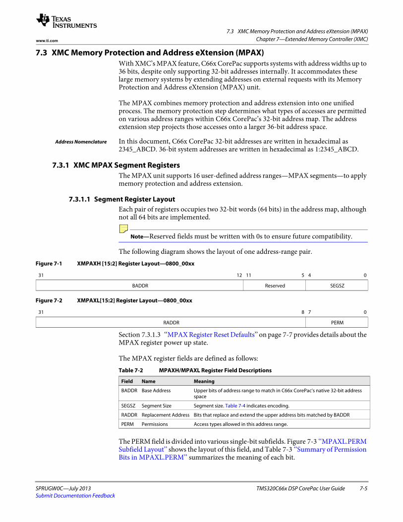
7.3 XMC Memory Protection and Address eXtension (MPAX)
SPRUGW0C—July 2013 TMS320C66x DSP CorePac User Guide 7-5Submit Documentation Feedback
Chapter 7—Extended Memory Controller (XMC)www.ti.com
7.3 XMC Memory Protection and Address eXtension (MPAX)With XMC’s MPAX feature, C66x CorePac supports systems with address widths up to 36 bits, despite only supporting 32-bit addresses internally. It accommodates these large memory systems by extending addresses on external requests with its Memory Protection and Address eXtension (MPAX) unit.
The MPAX combines memory protection and address extension into one unified process. The memory protection step determines what types of accesses are permitted on various address ranges within C66x CorePac’s 32-bit address map. The address extension step projects those accesses onto a larger 36-bit address space.
Address Nomenclature In this document, C66x CorePac 32-bit addresses are written in hexadecimal as 2345_ABCD. 36-bit system addresses are written in hexadecimal as 1:2345_ABCD.
7.3.1 XMC MPAX Segment RegistersThe MPAX unit supports 16 user-defined address ranges—MPAX segments—to apply memory protection and address extension.
7.3.1.1 Segment Register LayoutEach pair of registers occupies two 32-bit words (64 bits) in the address map, although not all 64 bits are implemented.
Note—Reserved fields must be written with 0s to ensure future compatibility.
The following diagram shows the layout of one address-range pair.
Section 7.3.1.3 ‘‘MPAX Register Reset Defaults’’ on page 7-7 provides details about the MPAX register power up state.
The MPAX register fields are defined as follows:
The PERM field is divided into various single-bit subfields. Figure 7-3 ‘‘MPAXL.PERM Subfield Layout’’ shows the layout of this field, and Table 7-3 ‘‘Summary of Permission Bits in MPAXL.PERM’’ summarizes the meaning of each bit.
Figure 7-1 XMPAXH [15:2] Register Layout—0800_00xx
31 12 11 5 4 0
BADDR Reserved SEGSZ
Figure 7-2 XMPAXL[15:2] Register Layout—0800_00xx
31 8 7 0
RADDR PERM
Table 7-2 MPAXH/MPAXL Register Field Descriptions
Field Name Meaning
BADDR Base Address Upper bits of address range to match in C66x CorePac’s native 32-bit address space
SEGSZ Segment Size Segment size. Table 7-4 indicates encoding.
RADDR Replacement Address Bits that replace and extend the upper address bits matched by BADDR
PERM Permissions Access types allowed in this address range.
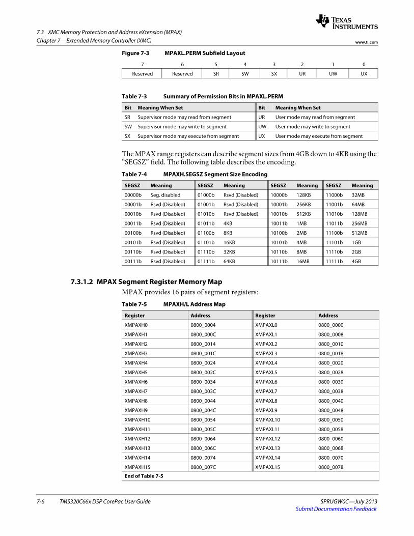
7.3 XMC Memory Protection and Address eXtension (MPAX)
7-6 TMS320C66x DSP CorePac User Guide SPRUGW0C—July 2013Submit Documentation Feedback
Chapter 7—Extended Memory Controller (XMC) www.ti.com
Figure 7-3 MPAXL.PERM Subfield Layout
The MPAX range registers can describe segment sizes from 4GB down to 4KB using the “SEGSZ” field. The following table describes the encoding.
7.3.1.2 MPAX Segment Register Memory MapMPAX provides 16 pairs of segment registers:
7 6 5 4 3 2 1 0
Reserved Reserved SR SW SX UR UW UX
Table 7-3 Summary of Permission Bits in MPAXL.PERM
Bit Meaning When Set Bit Meaning When Set
SR Supervisor mode may read from segment UR User mode may read from segment
SW Supervisor mode may write to segment UW User mode may write to segment
SX Supervisor mode may execute from segment UX User mode may execute from segment
Table 7-4 MPAXH.SEGSZ Segment Size Encoding
SEGSZ Meaning SEGSZ Meaning SEGSZ Meaning SEGSZ Meaning
00000b Seg. disabled 01000b Rsvd (Disabled) 10000b 128KB 11000b 32MB
00001b Rsvd (Disabled) 01001b Rsvd (Disabled) 10001b 256KB 11001b 64MB
00010b Rsvd (Disabled) 01010b Rsvd (Disabled) 10010b 512KB 11010b 128MB
00011b Rsvd (Disabled) 01011b 4KB 10011b 1MB 11011b 256MB
00100b Rsvd (Disabled) 01100b 8KB 10100b 2MB 11100b 512MB
00101b Rsvd (Disabled) 01101b 16KB 10101b 4MB 11101b 1GB
00110b Rsvd (Disabled) 01110b 32KB 10110b 8MB 11110b 2GB
00111b Rsvd (Disabled) 01111b 64KB 10111b 16MB 11111b 4GB
Table 7-5 MPAXH/L Address Map
Register Address Register Address
XMPAXH0 0800_0004 XMPAXL0 0800_0000
XMPAXH1 0800_000C XMPAXL1 0800_0008
XMPAXH2 0800_0014 XMPAXL2 0800_0010
XMPAXH3 0800_001C XMPAXL3 0800_0018
XMPAXH4 0800_0024 XMPAXL4 0800_0020
XMPAXH5 0800_002C XMPAXL5 0800_0028
XMPAXH6 0800_0034 XMPAXL6 0800_0030
XMPAXH7 0800_003C XMPAXL7 0800_0038
XMPAXH8 0800_0044 XMPAXL8 0800_0040
XMPAXH9 0800_004C XMPAXL9 0800_0048
XMPAXH10 0800_0054 XMPAXL10 0800_0050
XMPAXH11 0800_005C XMPAXL11 0800_0058
XMPAXH12 0800_0064 XMPAXL12 0800_0060
XMPAXH13 0800_006C XMPAXL13 0800_0068
XMPAXH14 0800_0074 XMPAXL14 0800_0070
XMPAXH15 0800_007C XMPAXL15 0800_0078
End of Table 7-5
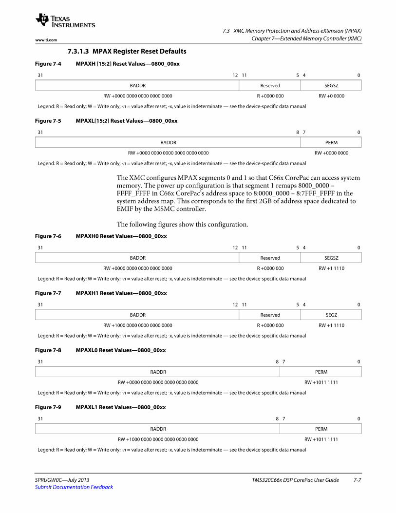
7.3 XMC Memory Protection and Address eXtension (MPAX)
SPRUGW0C—July 2013 TMS320C66x DSP CorePac User Guide 7-7Submit Documentation Feedback
Chapter 7—Extended Memory Controller (XMC)www.ti.com
7.3.1.3 MPAX Register Reset Defaults
The XMC configures MPAX segments 0 and 1 so that C66x CorePac can access system memory. The power up configuration is that segment 1 remaps 8000_0000 – FFFF_FFFF in C66x CorePac’s address space to 8:0000_0000 – 8:7FFF_FFFF in the system address map. This corresponds to the first 2GB of address space dedicated to EMIF by the MSMC controller.
The following figures show this configuration.
Figure 7-4 MPAXH [15:2] Reset Values—0800_00xx
31 12 11 5 4 0
BADDR Reserved SEGSZ
RW +0000 0000 0000 0000 0000 R +0000 000 RW +0 0000
Legend: R = Read only; W = Write only; -n = value after reset; -x, value is indeterminate — see the device-specific data manual
Figure 7-5 MPAXL[15:2] Reset Values—0800_00xx
31 8 7 0
RADDR PERM
RW +0000 0000 0000 0000 0000 0000 RW +0000 0000
Legend: R = Read only; W = Write only; -n = value after reset; -x, value is indeterminate — see the device-specific data manual
Figure 7-6 MPAXH0 Reset Values—0800_00xx
31 12 11 5 4 0
BADDR Reserved SEGSZ
RW +0000 0000 0000 0000 0000 R +0000 000 RW +1 1110
Legend: R = Read only; W = Write only; -n = value after reset; -x, value is indeterminate — see the device-specific data manual
Figure 7-7 MPAXH1 Reset Values—0800_00xx
31 12 11 5 4 0
BADDR Reserved SEGZ
RW +1000 0000 0000 0000 0000 R +0000 000 RW +1 1110
Legend: R = Read only; W = Write only; -n = value after reset; -x, value is indeterminate — see the device-specific data manual
Figure 7-8 MPAXL0 Reset Values—0800_00xx
31 8 7 0
RADDR PERM
RW +0000 0000 0000 0000 0000 0000 RW +1011 1111
Legend: R = Read only; W = Write only; -n = value after reset; -x, value is indeterminate — see the device-specific data manual
Figure 7-9 MPAXL1 Reset Values—0800_00xx
31 8 7 0
RADDR PERM
RW +1000 0000 0000 0000 0000 0000 RW +1011 1111
Legend: R = Read only; W = Write only; -n = value after reset; -x, value is indeterminate — see the device-specific data manual
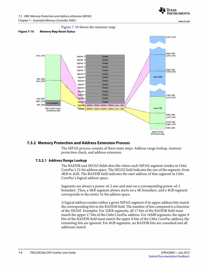
7.3 XMC Memory Protection and Address eXtension (MPAX)
7-8 TMS320C66x DSP CorePac User Guide SPRUGW0C—July 2013Submit Documentation Feedback
Chapter 7—Extended Memory Controller (XMC) www.ti.com
Figure 7-10 shows the memory map.Figure 7-10 Memory Map Reset Status
7.3.2 Memory Protection and Address Extension ProcessThe MPAX process consists of three main steps: Address range lookup, memory protection check, and address extension.
7.3.2.1 Address Range LookupThe BADDR and SEGSZ fields describe where each MPAX segment resides in C66x CorePac’s 32-bit address space. The SEGSZ field indicates the size of the segment, from 4KB to 4GB. The BADDR field indicates the start address of that segment in C66x CorePac’s logical address space.
Segments are always a power-of-2 size and start on a corresponding power-of-2 boundary. Thus, a 4KB segment always starts on a 4K boundary, and a 4GB segment corresponds to the entire 32-bit address space.
A logical address resides within a given MPAX segment if its upper address bits match the corresponding bits in the BADDR field. The number of bits compared is a function of the SEGSZ. Examples: For 32KB segments, all 17 bits of the BADDR field must match the upper 17 bits of the C66x CorePac address. For 16MB segments, the upper 8 bits of the BADDR field must match the upper 8 bits of the C66x CorePac address; the remaining bits are ignored. For 4GB segments, no BADDR bits are consulted and all addresses match.
Segment 1
Segment 0
DisabledSegment 2
DisabledSegment 3
DisabledSegment 4
DisabledSegment 5
DisabledSegment 6
DisabledSegment 7
DisabledSegment 8
DisabledSegment 9
DisabledSegment 10
DisabledSegment 11
DisabledSegment 12
DisabledSegment 13
DisabledSegment 14
DisabledSegment 15
C66x CorePac Logical32-bit Memory Map
Upper 60GB
System Physical36-bit Memory Map
Lower 4GB
0000_0000
7FFF_FFFF8000_0000
FFFF_FFFF
(not remappable )0BFF_FFFF0C00_0000 0:FFFF_FFFF
0:8000_00000:7FFF_FFFF
0:0C00_00000:0BFF_FFFF
0:0000_0000
1:0000_0000
F:FFFF_FFFF
7:FFFF_FFFF8:0000_0000
BADDR = 00000h; RADDR = 000000h; Size = 2GB
BADDR = 80000h; RADDR = 800000h; Size = 2GB
8:8000_00008:7FFF_FFFF
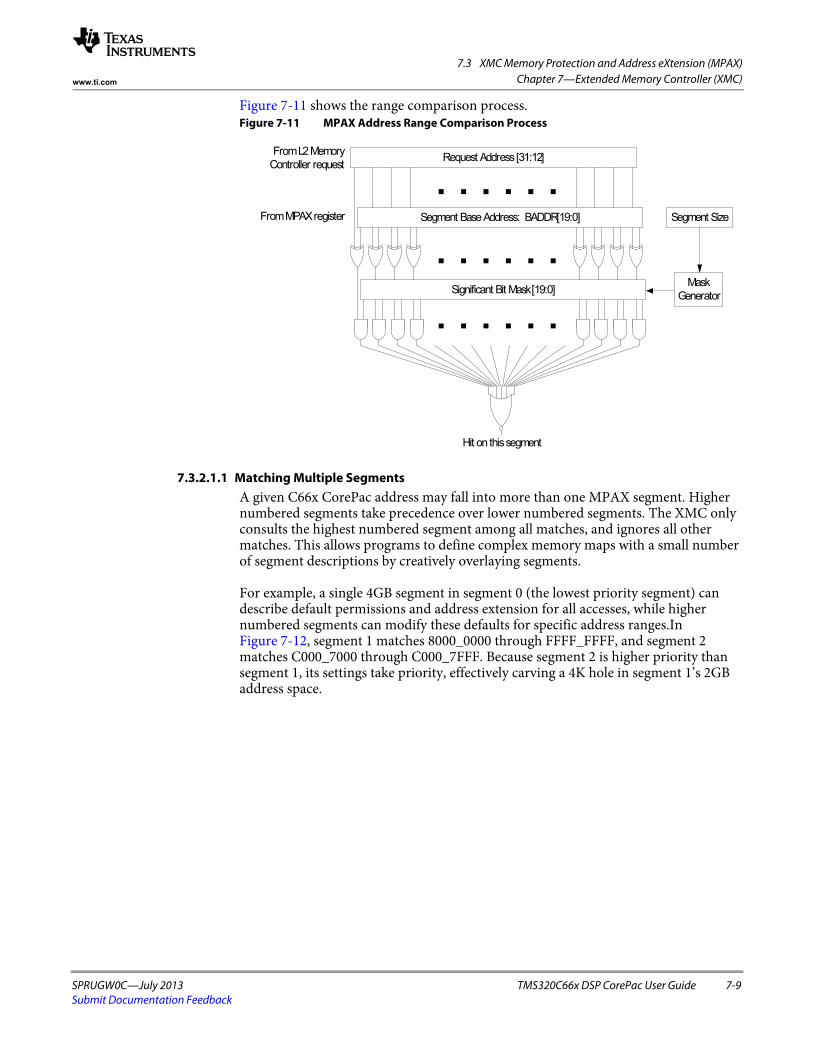
7.3 XMC Memory Protection and Address eXtension (MPAX)
SPRUGW0C—July 2013 TMS320C66x DSP CorePac User Guide 7-9Submit Documentation Feedback
Chapter 7—Extended Memory Controller (XMC)www.ti.com
Figure 7-11 shows the range comparison process.Figure 7-11 MPAX Address Range Comparison Process
7.3.2.1.1 Matching Multiple SegmentsA given C66x CorePac address may fall into more than one MPAX segment. Higher numbered segments take precedence over lower numbered segments. The XMC only consults the highest numbered segment among all matches, and ignores all other matches. This allows programs to define complex memory maps with a small number of segment descriptions by creatively overlaying segments.
For example, a single 4GB segment in segment 0 (the lowest priority segment) can describe default permissions and address extension for all accesses, while higher numbered segments can modify these defaults for specific address ranges.In Figure 7-12, segment 1 matches 8000_0000 through FFFF_FFFF, and segment 2 matches C000_7000 through C000_7FFF. Because segment 2 is higher priority than segment 1, its settings take priority, effectively carving a 4K hole in segment 1’s 2GB address space.
Request Address [31:12]From L2 Memory Controller request
From MPAX register Segment Size
Mask GeneratorSignificant Bit Mask[19:0]
Segment Base Address: BADDR[19:0]
Hit on this segment
. . . . . .
. . . . . .
. . . . . .

7.3 XMC Memory Protection and Address eXtension (MPAX)
7-10 TMS320C66x DSP CorePac User Guide SPRUGW0C—July 2013Submit Documentation Feedback
Chapter 7—Extended Memory Controller (XMC) www.ti.com
Figure 7-12 MPAX Segment Priority Example
7.3.2.1.2 Matching No SegmentsIt is possible that a given logical address matches no MPAX segments. MPAX treats these requests as matching a segment with zero permissions, and will generate a protection fault (MDMAERREVT event).
Note—“Zero permissions” means “all accesses disallowed” and is equivalent to PERM[5:0] = 000000b.
To establish default permissions (and a default address extension) for the entire memory map, use a low numbered segment, such as MPAX segment 0, with a large segment size. Addresses that do not match other segments will “fall through” and match this one.
7.3.2.1.3 Address Ranges Unaffected By MPAX
C66x CorePac does not present all accesses to XMC. Accesses to addresses 0000_0000 to 07FF_FFFF are decoded internally to C66x CorePac and not sent to XMC, and so these accesses never fall into any MPAX segment and are not checked against MPAX segment-based permissions. This address range includes the internal and external configuration busses, as well as the L1D, L1P and L2 memories. Because XMC never receives these requests, it does not include any special logic to handle requests in this address range.
BADDR = 00000h; RADDR = 000000h; Size = 2GB
BADDR = 80000h; RADDR = 080000h; Size = 2GBSegment 1
Segment 0
BADDR = C0007h; RADDR = 050042h; Size = 4KSegment 2
DisabledSegment 3
DisabledSegment 4
DisabledSegment 5
DisabledSegment 6
DisabledSegment 7
DisabledSegment 8
DisabledSegment 9
DisabledSegment 10
DisabledSegment 11
DisabledSegment 12
DisabledSegment 13
DisabledSegment 14
DisabledSegment 15
C66x CorePac 32-bit Memory Map
Upper 60GB
System 36-bit Memory Map
Lower 4GB0000_0000
7FFF_FFFF8000_0000
FFFF_FFFF
(not remappable )0BFF_FFFF0C00_0000
0:FFFF_FFFF
0:8000_00000:7FFF_FFFF
0:0C00_00000:0BFF_FFFF
0:0000_0000
1:0000_0000
F:FFFF_FFFF
0:5004_2xxx
0:C000_7xxx
C000_7xxx

7.3 XMC Memory Protection and Address eXtension (MPAX)
SPRUGW0C—July 2013 TMS320C66x DSP CorePac User Guide 7-11Submit Documentation Feedback
Chapter 7—Extended Memory Controller (XMC)www.ti.com
Furthermore, accesses to 0000_0000 through 0BFF_FFFF are considered accesses to memory mapped control registers. These addresses never match any segment. The MPAX unit does not modify these addresses, nor does it perform a segment-based protection check for accesses in this range, regardless of whether a segment overlaps this range.
Note—The XMC does specific checks on its own memory-mapped registers. This check is not done by the MPAX segment-based protection.
7.3.2.2 Address ExtensionMPAX address extension works by replacing the upper address bits of the logical address with corresponding bits from the replacement address (RADDR). The replacement address field is wider than the field it replaces, thus extending the 32-bit logical address to a 36-bit physical address.
7.3.2.2.1 Direct Accesses to MSMC RAM at its Native AddressIf the logical address for an access is in the local MSMC address range (0C00_0000 – 0CFF_FFFF by default)—then the upper 12 address bits of the 36 bit address are forced to “00C”, so that a C66x CorePac address of the form 0Cxx_xxxx will always result in an output address of the form 0:0Cxx_xxxx.
This allows moving ranges of addresses around within MSMC RAM, but it prohibits moving portions of MSMC RAM address space to different endpoints. C66x CorePac expects accesses in the address range to go to MSMC RAM, and uses this information to place the request on a “Fast RAM” path, eliminating a cycle of latency.
7.3.2.2.2 MSMC RAM Aliasing ScenariosC66x CorePac’s MARs only allows configuring the cacheability of 16MB ranges. It also hardwires the cacheability of certain address ranges, such as the range that corresponds to MSMC RAM. Using MPAX segments, programs can provide multiple aliases of various address ranges in the C66x CorePac’s 32-bit address space. The L2 controller treats accesses to these aliases as cacheable or non-cacheable based on the setting of the corresponding MAR register bits.
Thus, the cacheability of each alias can be controlled independently. This even applies to MSMC RAM: By making an alias of MSMC RAM at some other address, its cacheability becomes controlled by the corresponding MAR bits as well, rather than the default semantic applied to MSMC RAM when accessed at 0C00_0000 – 0C1F_FFFF. Accesses to MSMC RAM via this alias do not use the “Fast RAM” path and incur an additional cycle of latency.
Aliases provide a general mechanism for offering different semantics to a given address range. The following scenarios are applicable:
Table 7-6 MSMC RAM Aliasing Scenarios
Scenario
Cacheable in
Use CaseL1D L1P1 L2
MSMC RAM at native address(0C00_0000 – 0C1F_FFFF)
Yes Yes No Shared program and data (coherency managed by software)
MSMC RAM at alias; MAR.PC set to 1 Yes Yes Yes “Private” program/data in MSMC RAM
MSMC RAM at alias; MAR.PC set to 0 No Yes No “Coherent” shared memory in MSMC RAM (coherent because nothing is cached)1. L1P always caches program fetches when L1PCFG.L1PMODE > 0 and L1PCC.OPER = 0.

7.3 XMC Memory Protection and Address eXtension (MPAX)
7-12 TMS320C66x DSP CorePac User Guide SPRUGW0C—July 2013Submit Documentation Feedback
Chapter 7—Extended Memory Controller (XMC) www.ti.com
7.3.2.2.3 MSMC RAM Aliasing ExampleFigure 7-13 shows using 3 segments to map the MSMC RAM address space into C66x CorePac’s address space as three distinct 2MB ranges. By programming the MARs accordingly, the three ranges each could have different semantics, as detailed previously.
Figure 7-13 Applying Multiple Semantics to MSMC RAM with Aliases
7.3.2.2.4 Using MPAX to Access Low Memory (0:0000_0000 – 0:07FF_FFFF)C66x CorePac decodes logical addresses 0000_0000 – 07FF_FFFF internally, and does not send these to its MDMA port. The system, though, may still map peripherals in the corresponding physical address space 0:0000_0000 – 0:07FF_FFFF.
To access these system addresses, C66x CorePac must configure one or more of its MPAX segments with a RADDR that corresponds to this range. This enables C66x CorePac to access this address range through some other logical address window.
XMC’s own registers at 0800_0000 – 0800_FFFF are not accessible by any alias. XMC captures these accesses before MPAX modifies the address.
BADDR = 0C000h; RADDR = 00C000h; Size = 2MB
BADDR = 20000h; RADDR = 00C000h; Size = 2MB
C66x CorePac 32-bit Memory Map
0000_0000
FFFF_FFFF
(not remappable )0BFF_FFFF0Cxx_xxxx
0:0C1F_FFFF
0:0C00_0000
BADDR = 21000h; RADDR = 00C000h; Size = 2MB
20xx_xxxx21xx_xxxx
“Fast” MSMC RAM
MSMC RAM Alias 1
MSMC RAM Alias 2
MSMC RAM(2MB)

7.4 XMC Memory Protection Architecture Support
SPRUGW0C—July 2013 TMS320C66x DSP CorePac User Guide 7-13Submit Documentation Feedback
Chapter 7—Extended Memory Controller (XMC)www.ti.com
7.4 XMC Memory Protection Architecture SupportXMC’s MPAX unit provides a similar interface to protection fault reporting and controlling access to its own registers as the other blocks in C66x CorePac provide as part of the Memory Protection Architecture. The following subsections describe this support in detail.
7.4.1 Memory Protection Fault Reporting RegistersTo enable programs to diagnose a memory protection fault after an exception occurs, the XMC implements two registers (XMPFAR and XMPFSR) dedicated to storing information about the fault, and a third register (XMPFCR) to allow clearing the fault information. Figure 7-14, Figure 7-15 and Figure 7-16 show these registers.
The XMPFAR and XMPFSR registers store only enough information for one fault. Generally, the hardware records the information about the first fault and generates an exception for that fault only.
The XMC holds the fault information until software clears it by writing to 1 to XMPFCR.MPFCLR. XMC does nothing if software writes 0 to XMPFCR.MPFCLR. The XMC ignores the value written to bits 31:1 of XMPFCR. Programs, however, should write 0s to these bits.
See ‘‘Memory Protection Registers’’ on page 10-5 for more information.
Figure 7-14 Memory Protection Fault Status and Command Registers—(XMPFAR: 0800_0200)
31 0
Fault Address
R +0
Legend: R = Read only; W = Write only; -n = value after reset; -x, value is indeterminate — see the device-specific data manual
Figure 7-15 Memory Protection Fault Status and Command Registers—(XMPFSR 0800_0204)
31 9 8 7 6 5 0
Reserved LOCAL Reserved Access Type
R +0 R +0 R +0 R +0
Legend: R = Read only; W = Write only; -n = value after reset; -x, value is indeterminate — see the device-specific data manual
Figure 7-16 Memory Protection Fault Status and Command Registers—(XMPFCR 0800_0208)
31 1 0
Reserved MPFCLR
R +0 W +0
Legend: R = Read only; W = Write only; -n = value after reset; -x, value is indeterminate — see the device-specific data manual

7.5 Prefetch Buffers
7-14 TMS320C66x DSP CorePac User Guide SPRUGW0C—July 2013Submit Documentation Feedback
Chapter 7—Extended Memory Controller (XMC) www.ti.com
7.5 Prefetch BuffersPrefetch support in XMC aims to reduce the read miss penalty for streams of data entering C66x CorePac. Hence prefetching helps to reduce stall cycles and thereby improves memory read performance to MSMC RAM and EMIF. The XMC contains a multi-stream prefetch buffer. The buffer has 8 128-byte entries for prefetching data streams, in addition to a separate 4 entry by 32-byte program prefetch buffer. Streams are recognized through a simple prefetch filter.
Data requests from L1D and L2 are serviced by the 8 entry data prefetch buffer. Program requests from L1P and L2 are serviced by the 4 entry program prefetch buffer.
7.5.1 Data Prefetch BufferThe data prefetch buffer services read requests from both L1D and L2. L2 requests represent both program and data fetches to addresses that could reside anywhere in the system, including MSMC RAM and EMIF address spaces. The data prefetch buffer only considers data fetches.
The following sections detail how the data prefetch buffer detects streams with its stream detection filter, and generate prefetch requests once streams are detected.
7.5.1.1 CapacityThe data prefetch buffer contains 8 slots, each holding 128 bytes of data. Each slot has two 64-byte half-slots that XMC tracks separately. The entire slot is allocated as a single unit, although prefetch data and hits are tracked separately for the two halves.
In addition to the prefetch buffer, XMC implements stream detection filter built around a 12-address candidate buffer. This filter stores 12 potential stream head addresses as logical addresses, along with a single bit to indicate the predicted stream direction associated with that slot.
7.5.1.2 Allocation PolicyThe prefetch buffer and stream detection filter both use a FIFO allocation order built around a simple count. Each new allocation in the prefetch buffer uses the next slot number indicated by the count. Allocations in the stream detection filter’s candidate buffer do the same.
Thus, in the prefetch buffer, slot #0 gets used first, followed by slot #1, on up to slot #7. The count then wraps back to slot #0. Allocation in the stream detection filter’s candidate buffer proceeds similarly, starting at slot #0, counting to slot #11, and then wrapping back to slot #0.
The data prefetch buffer prevents a busy slot from getting reused until that slot becomes unbusy by stalling the allocation request as long as needed. A slot is busy if there is a hit pending resolution on that slot. This includes a hit that is waiting for a prefetch to return from the system, as well as a hit that is waiting to return its data to CorePac.
7.5.1.3 Stream Detection Filter (Candidate Buffer)The stream detection filter is built around a 12-entry candidate buffer. Entries in the candidate buffer have the potential to become prefetch streams.

7.5 Prefetch Buffers
SPRUGW0C—July 2013 TMS320C66x DSP CorePac User Guide 7-15Submit Documentation Feedback
Chapter 7—Extended Memory Controller (XMC)www.ti.com
7.5.1.3.1 Eligible Request CriteriaThe detection filter considers accesses that meet the following criteria:
• Prefetchable• Cache line fill for data• L1D line or non-critical half of an L2 line• Not already present in the prefetch buffer
Demand fetches that meet this criteria are compared against the existing entries in the candidate buffer. L1D requests are compared at 64 byte granularity, whereas L2 requests are compared at 128 byte granularity. What happens next depends on whether the demand fetch matches an entry in the candidate buffer.
7.5.1.3.2 No Matching Entry FoundThe filter allocates a new filter slot and places the predicted next address and predicted stream direction in this slot. The filter does not protect against redundant entries, as these are only possible when thrashing the cache, and thus should be rare.
7.5.1.3.3 Fetch Matches an Existing EntryIf the request does match an existing entry, the filter allocates a new stream slot in the prefetch buffer for the stream, initializing its address to the next address in that stream according to the direction bit stored with that slot. It also begins generating prefetches for that slot.
All new streams start while crossing a 128 byte (L1D stream) or 256 byte (L2 stream) boundary. This property is most important for L1D streams, as it guarantees that the first two prefetches for the stream always correspond to the two half-slots of a single slot.
7.5.2 Program Prefetch Buffer
The program prefetch buffer is a simple prefetch engine intended to service direct L1P requests and L2 program fetches. This buffer considers all cacheable, prefetchable program fetches as candidates for prefetching. The buffer supports a single program fetch stream.
7.5.2.1 CapacityThe prefetch buffer is organized as 4 slots containing 32 bytes (one fetch packet) each. The program prefetch buffer does not include a stream filter. Instead, it merely assumes programs fetch in the forward direction. It also only tracks one active program stream.
7.5.2.2 Allocation PolicyThe prefetch buffer allocates slots in FIFO order. That is, slot #0 gets allocated first, followed by slot #1, #2 and #3, before wrapping back to slot #0.
Each slot has two 32-byte data buffers associated with it, structured as a form of double-buffer. The prefetch buffer can reallocate a slot immediately if at least one of its two halves is not busy.

7.5 Prefetch Buffers
7-16 TMS320C66x DSP CorePac User Guide SPRUGW0C—July 2013Submit Documentation Feedback
Chapter 7—Extended Memory Controller (XMC) www.ti.com
7.5.3 Prefetch Coherence Issues—ExampleThe prefetch buffer reads ahead (either to higher or lower addresses depending on stream direction) on the various streams it has active. This can cause coherence issues when DSP cooperates with another master in prefetchable shared memory (MSMC or EMIF), since the prefetch buffer may read more data than the DSP requested.
Consider, for example, a double buffer in MSMC. Give it two halves, ping and pong, with pong appearing after ping in memory. DSP0 writes to the buffer and DSP1 reads from it, and the two synchronize via an interrupt. Now consider the following series of events:
1. DSP0 writes 1024 bytes to “ping.”2. DSP0 interrupts DSP1.3. DSP1 reads 1024 bytes from “ping.” This triggers the prefetch buffer to read an
additional 128 bytes beyond “ping” and into “pong.”4. DSP0 writes 1024 bytes to “pong.”5. DSP0 interrupts DSP1.6. DSP1 reads 1024 bytes from “pong.”
What happens in step 6?Depending on how quickly DSP1 reads the buffer in step 3, it could have triggered the prefetch the first part of “pong” before DSP0 filled it. Thus, in step #6, DSP1 could see old data in those first few bytes.
There are two primary solutions to this problem:• Space shared buffers apart so that the prefetch buffer won’t read past the end of
one and into the other.• Use XPFCMD.INV to invalidate the prefetch buffer when handing ownership of
a buffer between DSPs.For more information on XPFCMD.INV, see Section Section 7.6.1 ‘‘Prefetch Buffer Command Register: XPFCMD’’ on page 7-17.
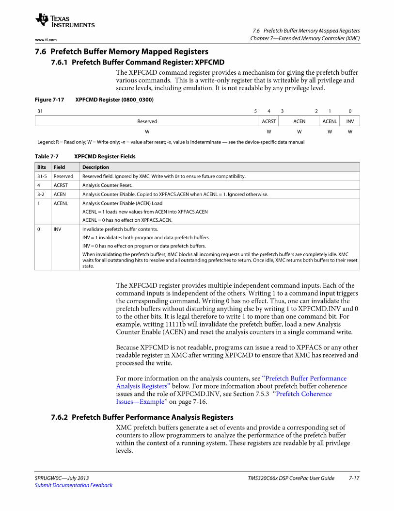
7.6 Prefetch Buffer Memory Mapped Registers
SPRUGW0C—July 2013 TMS320C66x DSP CorePac User Guide 7-17Submit Documentation Feedback
Chapter 7—Extended Memory Controller (XMC)www.ti.com
7.6 Prefetch Buffer Memory Mapped Registers7.6.1 Prefetch Buffer Command Register: XPFCMD
The XPFCMD command register provides a mechanism for giving the prefetch buffer various commands. This is a write-only register that is writeable by all privilege and secure levels, including emulation. It is not readable by any privilege level.
The XPFCMD register provides multiple independent command inputs. Each of the command inputs is independent of the others. Writing 1 to a command input triggers the corresponding command. Writing 0 has no effect. Thus, one can invalidate the prefetch buffers without disturbing anything else by writing 1 to XPFCMD.INV and 0 to the other bits. It is legal therefore to write 1 to more than one command bit. For example, writing 11111b will invalidate the prefetch buffer, load a new Analysis Counter Enable (ACEN) and reset the analysis counters in a single command write.
Because XPFCMD is not readable, programs can issue a read to XPFACS or any other readable register in XMC after writing XPFCMD to ensure that XMC has received and processed the write.
For more information on the analysis counters, see ‘‘Prefetch Buffer Performance Analysis Registers’’ below. For more information about prefetch buffer coherence issues and the role of XPFCMD.INV, see Section 7.5.3 ‘‘Prefetch Coherence Issues—Example’’ on page 7-16.
7.6.2 Prefetch Buffer Performance Analysis RegistersXMC prefetch buffers generate a set of events and provide a corresponding set of counters to allow programmers to analyze the performance of the prefetch buffer within the context of a running system. These registers are readable by all privilege levels.
Figure 7-17 XPFCMD Register (0800_0300)
31 5 4 3 2 1 0
Reserved ACRST ACEN ACENL INV
W W W W W
Legend: R = Read only; W = Write only; -n = value after reset; -x, value is indeterminate — see the device-specific data manual
Table 7-7 XPFCMD Register Fields
Bits Field Description
31-5 Reserved Reserved field. Ignored by XMC. Write with 0s to ensure future compatibility.
4 ACRST Analysis Counter Reset.
3-2 ACEN Analysis Counter ENable. Copied to XPFACS.ACEN when ACENL = 1. Ignored otherwise.
1 ACENL Analysis Counter ENable (ACEN) Load
ACENL = 1 loads new values from ACEN into XPFACS.ACEN
ACENL = 0 has no effect on XPFACS.ACEN.
0 INV Invalidate prefetch buffer contents.
INV = 1 invalidates both program and data prefetch buffers.
INV = 0 has no effect on program or data prefetch buffers.
When invalidating the prefetch buffers, XMC blocks all incoming requests until the prefetch buffers are completely idle. XMC waits for all outstanding hits to resolve and all outstanding prefetches to return. Once idle, XMC returns both buffers to their reset state.

7.6 Prefetch Buffer Memory Mapped Registers
7-18 TMS320C66x DSP CorePac User Guide SPRUGW0C—July 2013Submit Documentation Feedback
Chapter 7—Extended Memory Controller (XMC) www.ti.com
7.6.2.1 Analysis Counter Overview
Table 7-8 Prefetch Analysis Counter Descriptions
Register Name Description
XPFACS XMC PreFetch Analysis Counter Status
XPFAC0 - XPFAC3 XMC PreFetch Analysis Counter 0 through 3.
Figure 7-18 XMC PreFetch Analysis Counter Status—XPFACS (0800_0304)
31 4 3 2 1 0
Reserved ACEN Reserved
R, +0 R, +0 R, +0
Legend: R = Read only; W = Write only; -n = value after reset; -x, value is indeterminate — see the device-specific data manual
Figure 7-19 XMC PreFetch Analysis Counter—XPFAC0 (0800_0310)
31 20 19 0
Reserved SENT
R, +0 R, +0
Legend: R = Read only; W = Write only; -n = value after reset; -x, value is indeterminate — see the device-specific data manual
Figure 7-20 XMC PreFetch Analysis Counter—XPFAC1 (0800_0314)
31 20 19 0
Reserved CANCELED
R, +0 R, +0
Legend: R = Read only; W = Write only; -n = value after reset; -x, value is indeterminate — see the device-specific data manual
Figure 7-21 XMC PreFetch Analysis Counter—XPFAC2 (0800_0318)
31 20 19 0
Reserved HIT
R, +0 R, +0
Legend: R = Read only; W = Write only; -n = value after reset; -x, value is indeterminate — see the device-specific data manual
Figure 7-22 XMC PreFetch Analysis Counter—XPFAC3 (0800_031C)
31 20 19 0
Reserved MISS
R, +0 R, +0
Legend: R = Read only; W = Write only; -n = value after reset; -x, value is indeterminate — see the device-specific data manual
7.6 Prefetch Buffer Memory Mapped Registers
SPRUGW0C—July 2013 TMS320C66x DSP CorePac User Guide 7-19Submit Documentation Feedback
Chapter 7—Extended Memory Controller (XMC)www.ti.com
The data and program prefetch buffers each generate four different events associated with these counters. Each event corresponds to a single 32-byte dataphase of traffic. Therefore, events associated with L1D and L2 requests appear to count by 2s.
7.6.2.2 Counting ModesThe four events from each prefetch buffer get merged together prior to being counted according to the current setting of the analysis counter enable bits in XPFACS.ACEN.
7.6.2.3 Interpreting Analysis CountersThe counters increment based on the number of dataphases associated with each command. This allows program requests (which are a mix of 32-byte and 64-byte requests) to be freely added with data requests (which are all 64-byte requests), while still resulting in a meaningful count.
The counters are each 20 bits wide. This provides for a minimum of 2ms counting interval for a device operating at 1GHz, assuming XMC manages to keep its CLK/2 data interface saturated. All four counters halt when any one of XPFAC0 through XPFAC3 reaches 000F_FFFF. This allows one to determine the relative values of all four events even if the counters were not polled and reset frequently enough.
One can derive a number of useful values from the analysis count totals:
Table 7-9 Analysis Event Descriptions
Event Counter Description
SENT XPFAC0 A generated prefetch is being sent into the system.
CANCELED XPFAC1 A previously sent prefetch returned with a non-zero status or other error.
HIT XPFAC2 Prefetchable demand fetch received its data from a successful prefetch.
MISS XPFAC3 Prefetchable demand fetch is being sent into the system as a demand fetch.
Table 7-10 Analysis Counter Enable Modes (XPFACS.ACEN)
ACEN Event Counting Mode
00b Counters disabled. The counters will retain their value but will not increment.
01b Count program events only.
10b Count data events only.
11b Count both program and data events.
Table 7-11 Values Derivable from Prefetch Analysis Counters
Quantity Corresponding Expression
Total prefetchable demand fetches HIT + MISS
Total valid prefetches SENT - CANCELED
Total bandwidth used SENT - CANCELED + MISS
Wasted bandwidth (unused prefetches) SENT - CANCELED - HIT
Bandwidth amplification (relative %) 100% * ((SENT - CANCELED - HIT) / (HIT + MISS))
Hit rate (%) 100% * (HIT / (HIT + MISS))
Cancel rate (%) 100% * (CANCELED / SENT)

7.6 Prefetch Buffer Memory Mapped Registers
7-20 TMS320C66x DSP CorePac User Guide SPRUGW0C—July 2013Submit Documentation Feedback
Chapter 7—Extended Memory Controller (XMC) www.ti.com
7.6.3 Data Prefetch Buffer Address Visibility Register: XPFADDREight read-only status registers indicate the contents of the data prefetch buffer. These registers are readable by all privilege levels. Writes to these registers generate a protection fault (MDMAERREVT event).
Figure 7-23 shows the layout of these registers. Table 7-12 describes the fields in this register. Table 7-13 lists the address map for these registers.
There is no mechanism to observe the contents of the program prefetch buffer.
7.6.4 Prefetch Priority RegisterXMC adds an additional register, MDMAARBX, for controlling the priority of the prefetches it generates. Never give prefetch requests higher priority than demand requests. MDMAARBX is only writable by supervisor and emulation. This register is laid out as follows:
Figure 7-23 Prefetch Buffer Address Visibility Register Layout—XPFADDRn (0800_04xx)
31 7 6 5 4 3 2 1 0
ADDR DIR DPH DVH AVH DPL DVL AVL
R+0 R+0 R+0 R+0 R+0 R+0 R+0 R+0
Legend: R = Read only; W = Write only; -n = value after reset; -x, value is indeterminate — see the device-specific data manual
Table 7-12 XPFADDR Field Description
Bits Field Description
31-7 ADDR Bits 31:7 of the 32-bit logical address associated with this slot
6 DIR Direction of the stream. DIR = 0 for increasing, DIR = 1 for decreasing
5 DPH Data pending (prefetch sent) for upper 64 bytes of slot1
1. “Upper” and “lower” refer to the higher address half (0x40 - 0x7F) and lower address half (0x00 - 0x3F) of the slot, respectively.
4 DVH Data valid in upper 64 bytes of slot
3 AVH Address valid for upper 64 bytes of slot
2 DPL Data pending (prefetch sent) for lower 64 bytes of slot
1 DVL Data valid in lower 64 bytes of slot
0 AVL Address valid for lower 64 bytes of slot
Table 7-13 XPFADDR Address Map
Register Address Register Address
XPFADDR0 0800_0400 XPFADDR4 0800_0410
XPFADDR1 0800_0404 XPFADDR5 0800_0414
XPFADDR2 0800_0408 XPFADDR6 0800_0418
XPFADDR3 0800_040C XPFADDR7 0800_041C
Figure 7-24 MDMAARBX Register Layout (0800_0280)
31 19 18 16 15 0
Reserved PRI Reserved
R, +0 RW, +7 R, +0
Legend: R = Read only; W = Write only; -n = value after reset; -x, value is indeterminate — see the device-specific data manual

7.6 Prefetch Buffer Memory Mapped Registers
SPRUGW0C—July 2013 TMS320C66x DSP CorePac User Guide 7-21Submit Documentation Feedback
Chapter 7—Extended Memory Controller (XMC)www.ti.com
Table 7-14 XMC MDMA Arbitration Control Register (MDMAARBX) Field Descriptions
Bit Field Value Description
31-19 Reserved 0 Reserved
18-16 PRI 0-7h Priority field
0 Priority 0 (highest)
1h Priority 1
2h Priority 2
3h Priority 3
4h Priority 4
5h Priority 5
6h Priority 6
7h Priority 7 (lowest)
15-0 Reserved 0 Reserved
7.6 Prefetch Buffer Memory Mapped Registers
7-22 TMS320C66x DSP CorePac User Guide SPRUGW0C—July 2013Submit Documentation Feedback
Chapter 7—Extended Memory Controller (XMC) www.ti.com
SPRUGW0C—July 2013 TMS320C66x DSP CorePac User Guide 8-1Submit Documentation Feedback
Chapter 8
Bandwidth Management Architecture
8.1 "Introduction" on page 8-2 8.2 "Bandwidth Management Architecture" on page 8-3 8.3 "Bandwidth Management Registers" on page 8-4 8.4 "Privilege and Bandwidth Management Registers" on page 8-12
8.1 Introduction
8-2 TMS320C66x DSP CorePac User Guide SPRUGW0C—July 2013Submit Documentation Feedback
Chapter 8—Bandwidth Management Architecture www.ti.com
8.1 Introduction8.1.1 Purpose of the Bandwidth Management
The purpose of the bandwidth management is to assure that some of the requestors do not block the resources that are available in the C66x CorePac for extended periods of time.
Similar to the memory protection capability of the C66x DSP, bandwidth management (BWM) is defined globally (for the entire C66x CorePac), but implemented locally by each C66x CorePac resource. To this end, initializing bandwidth management consists of programming a common set of registers found in each of the C66x CorePac's resources.
8.1.2 Resource Bandwidth Protected by Bandwidth ManagementThe BWM control hardware manages the following four resources:
• Level 1 program (L1P) SRAM/cache • Level 1 data (L1D) SRAM/cache• Level 2 (L2) SRAM/cache• Memory-mapped registers configuration bus
8.1.3 Requestors Managed by Bandwidth ManagementEach of the following are potential requestors for the C66x CorePac resources listed in Section 8.1.2:
• DSP-initiated transfers: – Data access (for example, load/store)– Program access
• Programmable cache coherency operations (for example, writeback): – Block-based – Global
• Internal DMA (IDMA)-initiated transfers (and resulting coherency operations) • Externally-initiated slave DMA (SDMA) transfers (and resulting coherency
operations) 8.1.4 Terms and Definitions
See Appendix A on page A-1 for the terms and definitions used in this chapter.
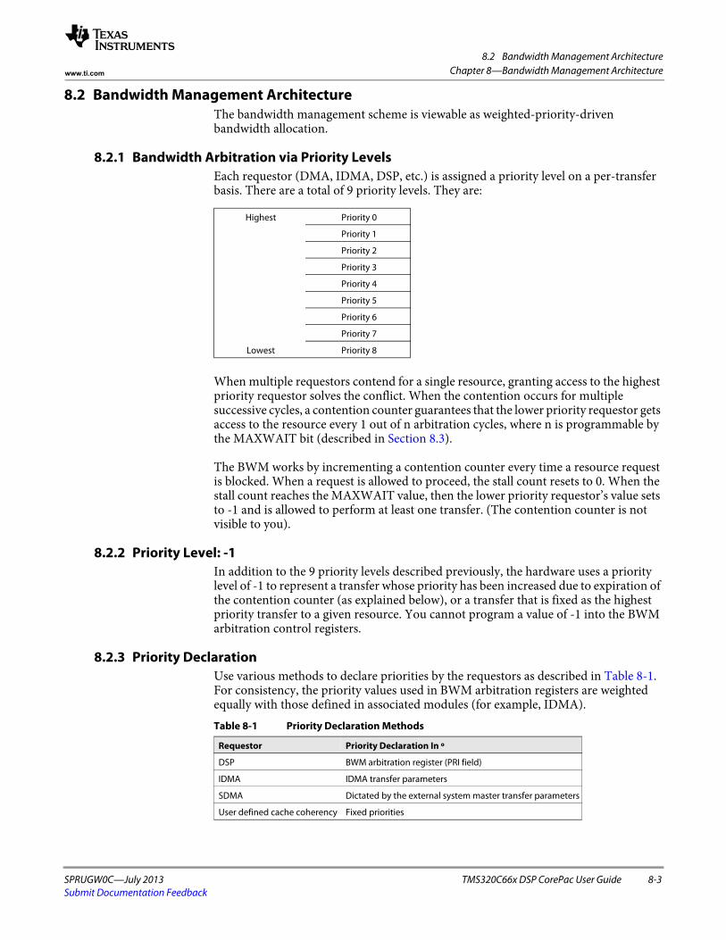
8.2 Bandwidth Management Architecture
SPRUGW0C—July 2013 TMS320C66x DSP CorePac User Guide 8-3Submit Documentation Feedback
Chapter 8—Bandwidth Management Architecturewww.ti.com
8.2 Bandwidth Management ArchitectureThe bandwidth management scheme is viewable as weighted-priority-driven bandwidth allocation.
8.2.1 Bandwidth Arbitration via Priority LevelsEach requestor (DMA, IDMA, DSP, etc.) is assigned a priority level on a per-transfer basis. There are a total of 9 priority levels. They are:
When multiple requestors contend for a single resource, granting access to the highest priority requestor solves the conflict. When the contention occurs for multiple successive cycles, a contention counter guarantees that the lower priority requestor gets access to the resource every 1 out of n arbitration cycles, where n is programmable by the MAXWAIT bit (described in Section 8.3).
The BWM works by incrementing a contention counter every time a resource request is blocked. When a request is allowed to proceed, the stall count resets to 0. When the stall count reaches the MAXWAIT value, then the lower priority requestor’s value sets to -1 and is allowed to perform at least one transfer. (The contention counter is not visible to you).
8.2.2 Priority Level: -1In addition to the 9 priority levels described previously, the hardware uses a priority level of -1 to represent a transfer whose priority has been increased due to expiration of the contention counter (as explained below), or a transfer that is fixed as the highest priority transfer to a given resource. You cannot program a value of -1 into the BWM arbitration control registers.
8.2.3 Priority DeclarationUse various methods to declare priorities by the requestors as described in Table 8-1. For consistency, the priority values used in BWM arbitration registers are weighted equally with those defined in associated modules (for example, IDMA).
Highest Priority 0
Priority 1
Priority 2
Priority 3
Priority 4
Priority 5
Priority 6
Priority 7
Lowest Priority 8
Table 8-1 Priority Declaration Methods
Requestor Priority Declaration In º
DSP BWM arbitration register (PRI field)
IDMA IDMA transfer parameters
SDMA Dictated by the external system master transfer parameters
User defined cache coherency Fixed priorities
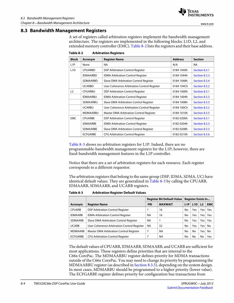
8.3 Bandwidth Management Registers
8-4 TMS320C66x DSP CorePac User Guide SPRUGW0C—July 2013Submit Documentation Feedback
Chapter 8—Bandwidth Management Architecture www.ti.com
8.3 Bandwidth Management RegistersA set of registers called arbitration registers implement the bandwidth management architecture. The registers are implemented in the following blocks: L1D, L2, and extended memory controller (EMC). Table 8-2 lists the registers and their base address.
Table 8-3 shows no arbitration registers for L1P. Indeed, there are no programmable-bandwidth management registers for the L1P; however, there are fixed-bandwidth management features in the L1P controller.
Notice that there are a set of arbitration registers for each resource. Each register corresponds to a different requestor.
The arbitration registers that belong to the same group (DSP, IDMA, SDMA, UC) have identical default values. They are generalized in Table 8-3 by calling the CPUARB, IDMAARB, SDMAARB, and UCARB registers.
The default values of CPUARB, IDMAARB, SDMAARB, and UCARB are sufficient for most applications. These registers define priorities that are internal to the C66x CorePac. The MDMAARBU register defines priority for MDMA transactions outside of the C66x CorePac. You may need to change its priority by programming the MDMAARBU register (as described in Section 8.3.5), depending on the system design. In most cases, MDMARBU should be programmed to a higher priority (lower value). The ECFGARBE register defines priority for configuration bus transactions from
Table 8-2 Arbitration Registers
Block Acronym Register Name Address Section
L1P None NA N/A NA
L1D CPUARBD DSP Arbitration Control Register 0184 1040h Section 8.3.1
IDMAARBD IDMA Arbitration Control Register 0184 1044h Section 8.3.3
SDMAARBD Slave DMA Arbitration Control Register 0184 1048h Section 8.3.4
UCARBD User Coherence Arbitration Control Register 0184 104Ch Section 8.3.2
L2 CPUARBU DSP Arbitration Control Register 0184 1000h Section 8.3.1
IDMAARBU IDMA Arbitration Control Register 0184 1004h Section 8.3.3
SDMAARBU Slave DMA Arbitration Control Register 0184 1008h Section 8.3.3
UCARBU User Coherence Arbitration Control Register 0184 100Ch Section 8.3.2
MDMAARBU Master DMA Arbitration Control Register 0184 1010h Section 8.3.5
EMC CPUARBE DSP Arbitration Control Register 0182 0200h Section 8.3.1
IDMAARBE IDMA Arbitration Control Register 0182 0204h Section 8.3.3
SDMAARBE Slave DMA Arbitration Control Register 0182 0208h Section 8.3.3
ECFGARBE CFG Arbitration Control Register 0182 0210h Section 8.3.6
Table 8-3 Arbitration Register Default Values
Acronym Register Name
Register Bit Default Value Register Exists In...
PRI MAXWAIT L1P L1D L2 EMC
CPUARB DSP Arbitration Control Register 1 16 No Yes Yes Yes
IDMAARB IDMA Arbitration Control Register NA 16 No Yes Yes Yes
SDMAARB Slave DMA Arbitration Control Register NA 1 No Yes Yes Yes
UCARB User Coherence Arbitration Control Register NA 32 No Yes Yes No
MDMAARB Master DMA Arbitration Control Register 7 NA No No Yes No
ECFGARBE CFG Arbitration Control Register 7 NA No No No Yes

8.3 Bandwidth Management Registers
SPRUGW0C—July 2013 TMS320C66x DSP CorePac User Guide 8-5Submit Documentation Feedback
Chapter 8—Bandwidth Management Architecturewww.ti.com
EMC.
8.3.1 DSP Arbitration Control Register (CPUARBD, CPUARBU, CPUARBE)The DSP arbitration control register (CPUARBD, CPUARBU, and CPUARBE) controls the bandwidth management of the DSP operations. The CPUARB register is shown in Figure 8-1 and described in Table 8-4. DSP-initiated transfers consist of two components:
1. The DSP issues program fetch transfers to the L1P controller, and the resulting L1P cache coherency operations (such as alloc/evict).
2. The DSP issues data/load store transfers to the L1D controller. The resulting L1D cache coherency operations (such as alloc/evict/long distance accesses) are in turn issued to the L2 controller.
Both program and data requests use CPUARB values to define the maximum wait time (MAXWAIT) and priority (PRI). CPUARB values do not only have an affect local to L1P or L1D. The priority/maximum wait time applied to L1D/L1P cache transactions is programmed at each block. These values are used to control arbitration at each relevant access within the C66x CorePac.
Similar to L1D/L1P (via CPUARBD), memory accesses made directly in L2 and EMC blocks (via the CPUARBU and CPUARBE registers, respectively) use the PRI and MAXWAIT field values locally for those blocks, and any further transactions resulting from these requests.
The default value of PRI is set so that the DSP transactions are the second to highest in the system. This should be a relatively typical value used in most systems, resulting in the DSP receiving highest priority most of the time, but, a short-real time deadline peripheral, such as a high speed serial port (that is typically programmed as the highest-priority transfer for SDMA requests) can interrupt the DSP transfers on a nearly immediate basis.
The DSP priority is run-time programmable, although you are expected to initialize the CPUARB registers at system initialization or accept the default values and leave them unchanged thereafter.
Figure 8-1 DSP Arbitration Control Register (CPUARBD, CPUARBU, CPUARBE)
31 19 18 16
Reserved PRI
R-0 R/W-1h
15 6 5 0
Reserved MAXWAIT
R-0 R/W-10h
Legend: R = Read only; W = Write only; -n = value after reset; -x, value is indeterminate — see the device-specific data manual
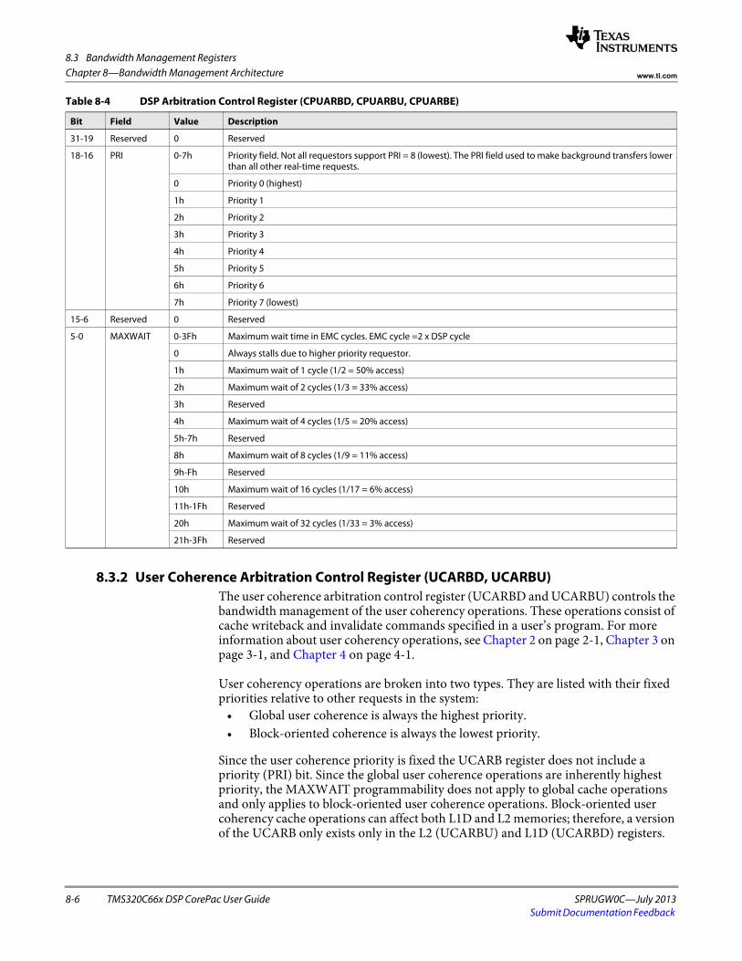
8.3 Bandwidth Management Registers
8-6 TMS320C66x DSP CorePac User Guide SPRUGW0C—July 2013Submit Documentation Feedback
Chapter 8—Bandwidth Management Architecture www.ti.com
8.3.2 User Coherence Arbitration Control Register (UCARBD, UCARBU)The user coherence arbitration control register (UCARBD and UCARBU) controls the bandwidth management of the user coherency operations. These operations consist of cache writeback and invalidate commands specified in a user’s program. For more information about user coherency operations, see Chapter 2 on page 2-1, Chapter 3 on page 3-1, and Chapter 4 on page 4-1.
User coherency operations are broken into two types. They are listed with their fixed priorities relative to other requests in the system:
• Global user coherence is always the highest priority.• Block-oriented coherence is always the lowest priority.
Since the user coherence priority is fixed the UCARB register does not include a priority (PRI) bit. Since the global user coherence operations are inherently highest priority, the MAXWAIT programmability does not apply to global cache operations and only applies to block-oriented user coherence operations. Block-oriented user coherency cache operations can affect both L1D and L2 memories; therefore, a version of the UCARB only exists only in the L2 (UCARBU) and L1D (UCARBD) registers.
Table 8-4 DSP Arbitration Control Register (CPUARBD, CPUARBU, CPUARBE)
Bit Field Value Description
31-19 Reserved 0 Reserved
18-16 PRI 0-7h Priority field. Not all requestors support PRI = 8 (lowest). The PRI field used to make background transfers lower than all other real-time requests.
0 Priority 0 (highest)
1h Priority 1
2h Priority 2
3h Priority 3
4h Priority 4
5h Priority 5
6h Priority 6
7h Priority 7 (lowest)
15-6 Reserved 0 Reserved
5-0 MAXWAIT 0-3Fh Maximum wait time in EMC cycles. EMC cycle =2 x DSP cycle
0 Always stalls due to higher priority requestor.
1h Maximum wait of 1 cycle (1/2 = 50% access)
2h Maximum wait of 2 cycles (1/3 = 33% access)
3h Reserved
4h Maximum wait of 4 cycles (1/5 = 20% access)
5h-7h Reserved
8h Maximum wait of 8 cycles (1/9 = 11% access)
9h-Fh Reserved
10h Maximum wait of 16 cycles (1/17 = 6% access)
11h-1Fh Reserved
20h Maximum wait of 32 cycles (1/33 = 3% access)
21h-3Fh Reserved
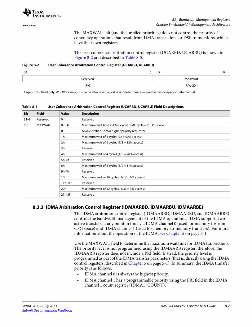
8.3 Bandwidth Management Registers
SPRUGW0C—July 2013 TMS320C66x DSP CorePac User Guide 8-7Submit Documentation Feedback
Chapter 8—Bandwidth Management Architecturewww.ti.com
The MAXWAIT bit (and the implied priorities) does not control the priority of coherency operations that result from DMA transactions or DSP transactions, which have their own registers.
The user coherence arbitration control register (UCARBD, UCARBU) is shown in Figure 8-2 and described in Table 8-5.
8.3.3 IDMA Arbitration Control Register (IDMAARBD, IDMAARBU, IDMAARBE)The IDMA arbitration control register (IDMAARBD, IDMAARBU, and IDMAARBE) controls the bandwidth management of the IDMA operations. IDMA supports two active transfers at any point in time via IDMA channel 0 (used for memory to/from CFG space) and IDMA channel 1 (used for memory-to-memory transfers). For more information about the operation of the IDMA, see Chapter 5 on page 5-1.
Use the MAXWAIT field to determine the maximum wait time for IDMA transactions. The priority level is not programmed using the IDMAARB register; therefore, the IDMAARB register does not include a PRI field. Instead, the priority level is programmed as part of the IDMA transfer parameters (that is, directly using the IDMA control registers, described in Chapter 5 on page 5-1). In summary, the IDMA transfer priority is as follows:
• IDMA channel 0 is always the highest priority. • IDMA channel 1 has a programmable priority using the PRI field in the IDMA
channel 1 count register (IDMA1_COUNT).
Figure 8-2 User Coherence Arbitration Control Register (UCARBD, UCARBU)
31 6 5 0
Reserved MAXWAIT
R-0 R/W-20h
Legend: R = Read only; W = Write only; -n = value after reset; -x, value is indeterminate — see the device-specific data manual
Table 8-5 User Coherence Arbitration Control Register (UCARBD, UCARBU) Field Descriptions
Bit Field Value Description
31-6 Reserved 0 Reserved
5-0 MAXWAIT 0-3Fh Maximum wait time in EMC cycles. EMC cycle = 2 DSP cycle.
0 Always stalls due to a higher priority requestor
1h Maximum wait of 1 cycle (1/2 = 50% access)
2h Maximum wait of 2 cycles (1/3 = 33% access)
3h Reserved
4h Maximum wait of 4 cycles (1/5 = 20% access)
5h-7h Reserved
8h Maximum wait of 8 cycles (1/9 = 11% access)
9h-Fh Reserved
10h Maximum wait of 16 cycles (1/17 = 6% access)
11h-1Fh Reserved
20h Maximum wait of 32 cycles (1/33 = 3% access)
21h-3Fh Reserved
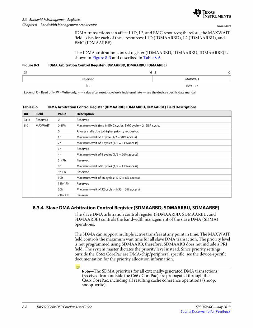
8.3 Bandwidth Management Registers
8-8 TMS320C66x DSP CorePac User Guide SPRUGW0C—July 2013Submit Documentation Feedback
Chapter 8—Bandwidth Management Architecture www.ti.com
IDMA transactions can affect L1D, L2, and EMC resources; therefore, the MAXWAIT field exists for each of these resources: L1D (IDMAARBD), L2 (IDMAARBU), and EMC (IDMAARBE).
The IDMA arbitration control register (IDMAARBD, IDMAARBU, IDMAARBE) is shown in Figure 8-3 and described in Table 8-6.
8.3.4 Slave DMA Arbitration Control Register (SDMAARBD, SDMAARBU, SDMAARBE)The slave DMA arbitration control register (SDMAARBD, SDMAARBU, and SDMAARBE) controls the bandwidth management of the slave DMA (SDMA) operations.
The SDMA can support multiple active transfers at any point in time. The MAXWAIT field controls the maximum wait time for all slave DMA transaction. The priority level is not programmed using SDMAARB; therefore, SDMAARB does not include a PRI field. The system master dictates the priority level instead. Since priority settings outside the C66x CorePac are DMA/chip/peripheral specific, see the device-specific documentation for the priority allocation information.
Note—The SDMA priorities for all externally-generated DMA transactions (received from outside the C66x CorePac) are propagated through the C66x CorePac, including all resulting cache coherence operations (snoop, snoop-write).
Figure 8-3 IDMA Arbitration Control Register (IDMAARBD, IDMAARBU, IDMAARBE)
31 6 5 0
Reserved MAXWAIT
R-0 R/W-10h
Legend: R = Read only; W = Write only; -n = value after reset; -x, value is indeterminate — see the device-specific data manual
Table 8-6 IDMA Arbitration Control Register (IDMAARBD, IDMAARBU, IDMAARBE) Field Descriptions
Bit Field Value Description
31-6 Reserved 0 Reserved
5-0 MAXWAIT 0-3Fh Maximum wait time in EMC cycles. EMC cycle = 2 DSP cycle.
0 Always stalls due to higher priority requestor.
1h Maximum wait of 1 cycle (1/2 = 50% access)
2h Maximum wait of 2 cycles (1/3 = 33% access)
3h Reserved
4h Maximum wait of 4 cycles (1/5 = 20% access)
5h-7h Reserved
8h Maximum wait of 8 cycles (1/9 = 11% access)
9h-Fh Reserved
10h Maximum wait of 16 cycles (1/17 = 6% access)
11h-1Fh Reserved
20h Maximum wait of 32 cycles (1/33 = 3% access)
21h-3Fh Reserved

8.3 Bandwidth Management Registers
SPRUGW0C—July 2013 TMS320C66x DSP CorePac User Guide 8-9Submit Documentation Feedback
Chapter 8—Bandwidth Management Architecturewww.ti.com
SDMA transactions can affect L1D, L2, and EMC resources; therefore, the MAXWAIT field exists for L1D (SDMAARBD), L2 (SDMAARBU), and EMC (SDMAARBE).
The slave DMA arbitration control register (SDMAARBD, SDMAARBU, SDMARBE) is shown in Figure 8-4 and described in Table 8-7.
8.3.5 Master DMA Arbitration Control Register (MDMAARBU)The master DMA arbitration control register (MDMAARBU) controls the priority levels of MDMA requests going out of CorePac. It controls the priority levels used by the L2 memory controller when sending requests to XMC.
The master DMA arbitration control register (MDMAARBU) is shown in Figure 8-5 and described in Table 8-8.
Figure 8-4 Slave DMA Arbitration Control Register (SDMAARBD, SDMAARBU, SDMAARBE)
31 6 5 0
Reserved MAXWAIT
R-0 R/W-01h
Legend: R = Read only; W = Write only; -n = value after reset; -x, value is indeterminate — see the device-specific data manual
Table 8-7 Slave DMA Arbitration Control Register ((SDMAARBD, SDMAARBU, SDMARBE) Field Descriptions
Bit Field Value Description
31-6 Reserved 0 Reserved
5-0 MAXWAIT 0-3Fh Maximum wait time in EMC cycles. EMC cycle = 2 DSP cycle.
0 Always stalls due to higher priority requestor
1h Maximum wait of 1 cycle (1/2 = 50% access)
2h Maximum wait of 2 cycles (1/3 = 33% access)
3h Reserved
4h Maximum wait of 4 cycles (1/5 = 20% access)
5h-7h Reserved
8h Maximum wait of 8 cycles (1/9 = 11% access)
9h-Fh Reserved
10h Maximum wait of 16 cycles (1/17 = 6% access)
11h-1Fh Reserved
20h Maximum wait of 32 cycles (1/33 = 3% access)
21h-3Fh Reserved
Figure 8-5 Master DMA Arbitration Control Register (MDMAARBU)
31 27 26 24 23 19 18 16
Reserved UPRI Reserved PRI
R-0 R/W-6h R-0 R/W-7h
15 0
Reserved
R-0
Legend: R = Read only; W = Write only; -n = value after reset; -x, value is indeterminate — see the device-specific data manual

8.3 Bandwidth Management Registers
8-10 TMS320C66x DSP CorePac User Guide SPRUGW0C—July 2013Submit Documentation Feedback
Chapter 8—Bandwidth Management Architecture www.ti.com
Note—It is a requirement to have urgent-priority (UPRI) field less than or equal to normal-priority (PRI) field. To ensure that, incorrect writes to MDMAARBU register where the numerical value of MDMAARBU.PRI is greater than MDMAARBU.UPRI will be dropped and will trigger a DSP memory protection fault from L2 memory controller. The values of priority fields will not be auto-corrected by L2 memory controller. The old value of MDMAARBU register will be retained.
When sending requests external to CorePac, L2 memory controller picks one of two priority values to send to XMC. For normal-priority requests, it uses the value of MDMAARBU.PRI. For urgent-priority requests, it uses the value of MDMAARBU.UPRI. Most L2 memory controller requests to XMC are not urgent. Only the following request types are urgent requests:
• L1D read miss• L1P fetch for a branch target• Critical subline of an L2 allocate
Table 8-8 Master DMA Arbitration Control Register (MDMAARBU) Field Descriptions
Bit Field Value Description
31-27 Reserved 0 Reserved
26-24 UPRI 0-7h Urgent priority field. This field must be either equal or lesser than PRI field.
0 Priority 0 (highest)
1h Priority 1
2h Priority 2
3h Priority 3
4h Priority 4
5h Priority 5
6h Priority 6
7h Priority 7 (lowest)
23-19 Reserved 0 Reserved
18-16 PRI 0-7h Normal priority field. This field must be either equal or greater than UPRI field.
Not all requestors support PRI = 8 (lowest), this is used to make background transfers lower than all other real-time requests.
0 Priority 0 (highest)
1h Priority 1
2h Priority 2
3h Priority 3
4h Priority 4
5h Priority 5
6h Priority 6
7h Priority 7 (lowest)
15-0 Reserved 0 Reserved

8.3 Bandwidth Management Registers
SPRUGW0C—July 2013 TMS320C66x DSP CorePac User Guide 8-11Submit Documentation Feedback
Chapter 8—Bandwidth Management Architecturewww.ti.com
8.3.6 CFG Arbitration Control Register (ECFGARBE)The CFG arbitration control register (ECFGARBE) controls the priority for the configuration bus transactions from EMC.
The CFG arbitration control register (ECFGARBE) is shown in Figure 8-5 and described in Table 8-8.
Figure 8-6 CFG Arbitration Control Register (ECFGARBE)
31 19 18 16
Reserved PRI
R-0 R/W-7h
15 0
Reserved
R-0
Legend: R = Read only; W = Write only; -n = value after reset; -x, value is indeterminate — see the device-specific data manual
Table 8-9 CFG Arbitration Control Register (ECFGARBE) Field Descriptions
Bit Field Value Description
31-19 Reserved 0 Reserved
18-16 PRI 0-7h Priority field: Not all requestors support PRI = 8 (lowest), this is used to make background transfers lower than all other real-time requests.
0 Priority 0 (highest)
1h Priority 1
2h Priority 2
3h Priority 3
4h Priority 4
5h Priority 5
6h Priority 6
7h Priority 7 (lowest)
15-0 Reserved 0 Reserved

8.4 Privilege and Bandwidth Management Registers
8-12 TMS320C66x DSP CorePac User Guide SPRUGW0C—July 2013Submit Documentation Feedback
Chapter 8—Bandwidth Management Architecture www.ti.com
8.4 Privilege and Bandwidth Management RegistersTable 8-10 summarizes which bandwidth management registers are accessible according to a person's role (supervisor or user).Table 8-10 Permissions for Bandwidth Management Registers
Register Supervisor User
CPUARBD R/W R
IDMAARBD R/W R
SDMAARBD R/W R
UCARBD R/W R
CPUARBU R/W R
IDMAARBU R/W R
SDMAARBU R/W R
UCARBU R/W R
MDMAARBU R/W R
CPUARBE R/W R
IDMAARBE R/W R
SDMAARBE R/W R
ECFGARBE R/W R

SPRUGW0C—July 2013 TMS320C66x DSP CorePac User Guide 9-1Submit Documentation Feedback
Chapter 9
Interrupt Controller
9.1 "Introduction" on page 9-2 9.2 "Interrupt Controller Architecture" on page 9-4 9.3 "C66x CorePac Events" on page 9-14 9.4 "Interrupt Controller - DSP Interaction" on page 9-15 9.5 "Registers" on page 9-17
9.1 Introduction
9-2 TMS320C66x DSP CorePac User Guide SPRUGW0C—July 2013Submit Documentation Feedback
Chapter 9—Interrupt Controller www.ti.com
9.1 IntroductionThis section describes the purpose and features of the interrupt controller.
9.1.1 Purpose of the C66x CorePac Interrupt Controller (INTC)The C66x CorePac provides a large assortment of system events. The interrupt controller provides a way to select the necessary events and route them to the appropriate DSP interrupt and exception inputs.
While you can use many of these same system events to drive other peripherals, such as the EDMA, the C66x CorePac’s interrupt controller is dedicated to managing the DSP.
9.1.2 Features
Note—The nonmaskable interrupt (NMI) is not supported on all C6000 devices, see your device-specific data manual for more information.
The interrupt controller interfaces the system events to the DSP’s interrupt and exceptions inputs. The interrupt controller supports up to 128 system events.
There are 128 system events that act as inputs to the interrupt controller. They consist of both internally-generated events (within the C66x CorePac) and chip-level events. The list of events are enumerated later in Section 9.3. In addition to these 128 events, the INTC register also receives the non-maskable and reset events and routes straight through to the DSP.
The interrupt controller outputs various signals to the C66x DSP from these event inputs:
• One maskable, hardware exception (EXCEP)• Twelve maskable hardware interrupts (INT4 through INT15) • One non-maskable signal that you can use as either an interrupt or an exception
(NMI) • One reset signal (RESET)
For more information on these DSP interrupt/exception signals, see the C66x DSP and Instruction Set Reference Guide (SPRUGH7) in ‘‘Related Documentation from Texas Instruments’’ on page ø-xx.
The interrupt controller includes the following modules to facilitate the routing of events to interrupts and exceptions:
• Interrupt Selector - routes any of the system events to the 12 maskable interrupts• Event Combiner - reduces the large number of system events down to four • Exception Combiner - lets any of the system events be grouped together for the
single hardware exception input

9.1 Introduction
SPRUGW0C—July 2013 TMS320C66x DSP CorePac User Guide 9-3Submit Documentation Feedback
Chapter 9—Interrupt Controllerwww.ti.com
9.1.3 Functional Block DiagramFigure 9-1 C66x CorePac Interrupt Controller Block Diagram
9.1.4 Terms and DefinitionsTerms of specific importance in this chapter are:
• System Event: any signal that generates internally or externally that is intended to notify the DSP that some activity has occurred and/or requires a response.
• Interrupts: provide the means to redirect normal program flow due to the presence of an external or internal hardware signal (event).
Exceptions are similar to interrupts in that they also redirect program flow, but exceptions are normally associated with error conditions in the system.
See Appendix A on page A-1 and Appendix B on page B-1 of this document for additional definitions of the terms used in this chapter. Appendix A on page A-1 describes general terms used throughout this reference guide and Appendix B on page B-1 defines terms related to the memory and cache architecture.
Exceptioncombiner
combinerEvent
Interruptselector
flagsEvent
RESET
NMEVT
EVT[3:0]
EVT[127:4]
RESET
EXCEP
NMI
INT[15:4]
IDROPmask
IDROP[15:4]INTERR
Interrupt controller CPU
AEG event
selector
IACK
INUM[4:0]
(AdvancedAEG
Generator)Event

9.2 Interrupt Controller Architecture
9-4 TMS320C66x DSP CorePac User Guide SPRUGW0C—July 2013Submit Documentation Feedback
Chapter 9—Interrupt Controller www.ti.com
9.2 Interrupt Controller ArchitectureThe C66x CorePac interrupt controller is designed to provide flexible management of system events. This functionality is implemented using the set of registers listed in Table 9-1. These registers are mentioned throughout this chapter. Detailed descriptions for these registers are provided in Section 9.5.
9.2.1 Event Registers The interrupt controller contains a set of registers to manage the status of the system events received by the controller. The registers can be grouped as follows:
• Event flag registers (EVTFLAGx) • Clear flag registers (EVTCLRx)• Set flag registers (EVTSETx)
The event flag registers capture all system events that are received by the Interrupt Controller. There are four 32-bit registers to cover the 124 system event inputs. Each system event is mapped to a specific flag bit (EFxx) in one of the event flag registers.
The generic event flag register structure is shown in Figure 9-2.
All 124 system events are individually mapped to a bit of the four 32-bit EVTFLAGx registers. This leaves the least significant four bits of EVTFLAG0 (EF03:EF00) not associated with a system event. These four bits are reserved and always zero. That is, there are no system event inputs that correspond to these fields. Instead, the system
Table 9-1 Interrupt Controller Registers
Register Description Type
EVTFLAG [3:0] Event Flag Registers Status
EVTCLR [3:0] Event Clear Registers Command
EVTSET [3:0] Event Set Registers Command
EVTMASK [3:0] Event Mask Registers Control
MEVTFLAG [3:0] Masked Event Flag Registers Status
EXPMASK [3:0] Exception Mask Registers Control
MEXPFLAG [3:0] Masked Exception Flag Registers Status
INTMUX [3:1] Interrupt Mux Registers Control
AEGMUX [1:0] Advanced Event Generator Mux Registers Control
INTXSTAT Interrupt Exception Status Register Status
INTXCLR Interrupt Exception Clear Register Command
INTDMASK Dropped Interrupt Mask Register Control
Figure 9-2 Event Flag Register Structure
31 30 29 28 27 26 25 24 23 22 21 20 19 18 17 16
EF EF EF EF EF EF EF EF EF EF EF EF EF EF EF EF
R-0 R-0 R-0 R-0 R-0 R-0 R-0 R-0 R-0 R-0 R-0 R-0 R-0 R-0 R-0 R-0
15 14 13 12 11 10 9 8 7 6 5 4 3 2 1 0
EF EF EF EF EF EF EF EF EF EF EF EF EF EF EF EF
R-0 R-0 R-0 R-0 R-0 R-0 R-0 R-0 R-0 R-0 R-0 R-0 R-0 R-0 R-0 R-0
Legend: R = Read only; W = Write only; -n = value after reset; -x, value is indeterminate — see the device-specific data manual

9.2 Interrupt Controller Architecture
SPRUGW0C—July 2013 TMS320C66x DSP CorePac User Guide 9-5Submit Documentation Feedback
Chapter 9—Interrupt Controllerwww.ti.com
events associated with events 00 through 03 are generated internal (to the Interrupt Controller) by the Event Combiner, which are routed to the Interrupt Selector, as shown in Figure 9-1.
The event flags (EFxx) are latched register bits; that is, they retain the value of 1 for any event received. The EVTFLAGx registers are read-only and must be cleared through the write-only Event Clear registers EVTCLR[3:0].
Use the event clear registers to clear the event flag registers. There are four 32-bit event clear registers. The fields of these registers map one-to-one with the fields of the event flag registers. Writing a 1 to a specific field in an event clear register causes the corresponding event flag register field to clear.
The event clear register structure is shown in Figure 9-3.
The event set registers are conceptually similar to the event clear registers. Use the event set registers to manually set any bit(s) within the event flag registers (e.g., it may be beneficial to use the event set registers to generate interrupts when testing interrupt service routines). There are four 32-bit event set registers whose fields map one-to-one to the fields of the event flag registers. Writing a 1 to a specific field in an event set register causes the corresponding event flag register to set to 1.
The event set register structure is shown in Figure 9-4.
The interrupt controller uses the event clear and event set registers, rather than writing directly to the event flag registers to prevent potential race conditions. Without these additional registers, the DSP might have otherwise accidentally cleared event flags set during a read-modify-write operation of the flag bits.
Figure 9-3 Event Clear Register Structure
31 30 29 28 27 26 25 24 23 22 21 20 19 18 17 16
EC EC EC EC EC EC EC EC EC EC EC EC EC EC EC EC
W-0 W-0 W-0 W-0 W-0 W-0 W-0 W-0 W-0 W-0 W-0 W-0 W-0 W-0 W-0 W-0
15 14 13 12 11 10 9 8 7 6 5 4 3 2 1 0
EC EC EC EC EC EC EC EC EC EC EC EC EC EC EC EC
W-0 W-0 W-0 W-0 W-0 W-0 W-0 W-0 W-0 W-0 W-0 W-0 W-0 W-0 W-0 W-0
Legend: R = Read only; W = Write only; -n = value after reset; -x, value is indeterminate — see the device-specific data manual
Figure 9-4 Event Set Register Structure
31 30 29 28 27 26 25 24 23 22 21 20 19 18 17 16
ES ES ES ES ES ES ES ES ES ES ES ES ES ES ES ES
W-0 W-0 W-0 W-0 W-0 W-0 W-0 W-0 W-0 W-0 W-0 W-0 W-0 W-0 W-0 W-0
15 14 13 12 11 10 9 8 7 6 5 4 3 2 1 0
ES ES ES ES ES ES ES ES ES ES ES ES ES ES ES ES
W-0 W-0 W-0 W-0 W-0 W-0 W-0 W-0 W-0 W-0 W-0 W-0 W-0 W-0 W-0 W-0
Legend: R = Read only; W = Write only; -n = value after reset; -x, value is indeterminate — see the device-specific data manual

9.2 Interrupt Controller Architecture
9-6 TMS320C66x DSP CorePac User Guide SPRUGW0C—July 2013Submit Documentation Feedback
Chapter 9—Interrupt Controller www.ti.com
If a new event is received during the same cycle, a clear is specified via an EVTCLRx register, the new event input takes precedence as an additional precaution against missing events.
9.2.2 Event CombinerThe event combiner (Figure 9-5) allows multiple system events to be combined into a single event. The combined events are routed to the interrupt selector. This allows the DSP to service all available system events even though the DSP only has twelve available interrupts. Figure 9-5 Event Combiner
The basic concept of the event combiner is to perform an OR operation on a subset of the system event flags (described in Table 9-2). The results of the OR operation are provided as a new “combined” event).
The event combiner divides the 124 system events into four groups. The first group includes events 4 through 31, the second group includes events 32 through 63, the third group includes events 64 through 95, and the fourth group includes events 96 through 127. You can combine events within each group to provide a new “combined” event. These new events are designated EVT0, EVT1, EVT2, and EVT3. These events are routed to the interrupt selector along with the original 124 system events for a combined total of 128 events.
For each group there is an event mask register.
The general structure of the event mask register is shown in Figure 9-6.
EVT MASK
− EVT0
EVT4 −
MEVT FLAG
− EVT1
EVT31 −EVT32 −
EMxx MEFxx
EVT63 −
EMxx MEFxx
− EVT2
EVT64 −
EVT95 −
EMxx MEFxx
− EVT3
EVT96 −
EVT127 −
EMxxx MEFxxx
Figure 9-6 Event Mask Register Structure
31 30 29 28 27 26 25 24 23 22 21 20 19 18 17 16
EM EM EM EM EM EM EM EM EM EM EM EM EM EM EM EM
R/W-0 R/W-0 R/W-0 R/W-0 R/W-0 R/W-0 R/W-0 R/W-0 R/W-0 R/W-0 R/W-0 R/W-0 R/W-0 R/W-0 R/W-0 R/W-0
15 14 13 12 11 10 9 8 7 6 5 4 3 2 1 0
EM EM EM EM EM EM EM EM EM EM EM EM EM EM EM EM
R/W-0 R/W-0 R/W-0 R/W-0 R/W-0 R/W-0 R/W-0 R/W-0 R/W-0 R/W-0 R/W-0 R/W-0 R/W-0 R/W-0 R/W-0 R/W-0
Legend: R = Read only; W = Write only; -n = value after reset; -x, value is indeterminate — see the device-specific data manual
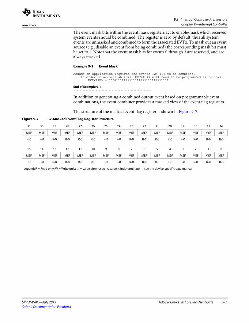
9.2 Interrupt Controller Architecture
SPRUGW0C—July 2013 TMS320C66x DSP CorePac User Guide 9-7Submit Documentation Feedback
Chapter 9—Interrupt Controllerwww.ti.com
The event mask bits within the event mask registers act to enable/mask which received system events should be combined. The register is zero by default, thus all system events are unmasked and combined to form the associated EVTx. To mask out an event source (e.g., disable an event from being combined) the corresponding mask bit must be set to 1. Note that the event mask bits for events 0 through 3 are reserved, and are always masked.
Example 9-1 Event Mask
Assume an application requires the events 124-127 to be combined. In order to accomplish this, EVTMASK3 will need to be programmed as follows:
EVTMASK3 = 00001111111111111111111111111111
End of Example 9-1
In addition to generating a combined output event based on programmable event combinations, the event combiner provides a masked view of the event flag registers.
The structure of the masked event flag register is shown in Figure 9-7. Figure 9-7 32-Masked Event Flag Register Structure
31 30 29 28 27 26 25 24 23 22 21 20 19 18 17 16
MEF MEF MEF MEF MEF MEF MEF MEF MEF MEF MEF MEF MEF MEF MEF MEF
R-0 R-0 R-0 R-0 R-0 R-0 R-0 R-0 R-0 R-0 R-0 R-0 R-0 R-0 R-0 R-0
15 14 13 12 11 10 9 8 7 6 5 4 3 2 1 0
MEF MEF MEF MEF MEF MEF MEF MEF MEF MEF MEF MEF MEF MEF MEF MEF
R-0 R-0 R-0 R-0 R-0 R-0 R-0 R-0 R-0 R-0 R-0 R-0 R-0 R-0 R-0 R-0
Legend: R = Read only; W = Write only; -n = value after reset; -x, value is indeterminate — see the device-specific data manual
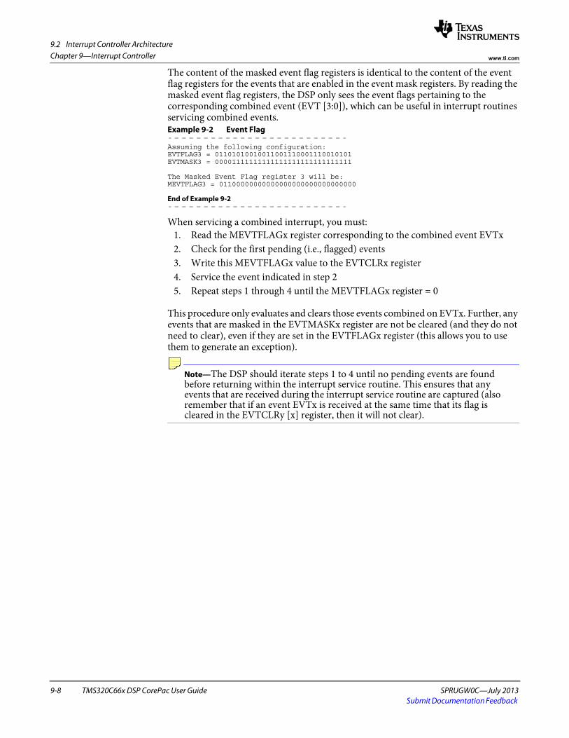
9.2 Interrupt Controller Architecture
9-8 TMS320C66x DSP CorePac User Guide SPRUGW0C—July 2013Submit Documentation Feedback
Chapter 9—Interrupt Controller www.ti.com
The content of the masked event flag registers is identical to the content of the event flag registers for the events that are enabled in the event mask registers. By reading the masked event flag registers, the DSP only sees the event flags pertaining to the corresponding combined event (EVT [3:0]), which can be useful in interrupt routines servicing combined events.Example 9-2 Event Flag
Assuming the following configuration:EVTFLAG3 = 01101010010011001110001110010101EVTMASK3 = 00001111111111111111111111111111
The Masked Event Flag register 3 will be:MEVTFLAG3 = 01100000000000000000000000000000
End of Example 9-2
When servicing a combined interrupt, you must: 1. Read the MEVTFLAGx register corresponding to the combined event EVTx2. Check for the first pending (i.e., flagged) events 3. Write this MEVTFLAGx value to the EVTCLRx register 4. Service the event indicated in step 2 5. Repeat steps 1 through 4 until the MEVTFLAGx register = 0
This procedure only evaluates and clears those events combined on EVTx. Further, any events that are masked in the EVTMASKx register are not be cleared (and they do not need to clear), even if they are set in the EVTFLAGx register (this allows you to use them to generate an exception).
Note—The DSP should iterate steps 1 to 4 until no pending events are found before returning within the interrupt service routine. This ensures that any events that are received during the interrupt service routine are captured (also remember that if an event EVTx is received at the same time that its flag is cleared in the EVTCLRy [x] register, then it will not clear).
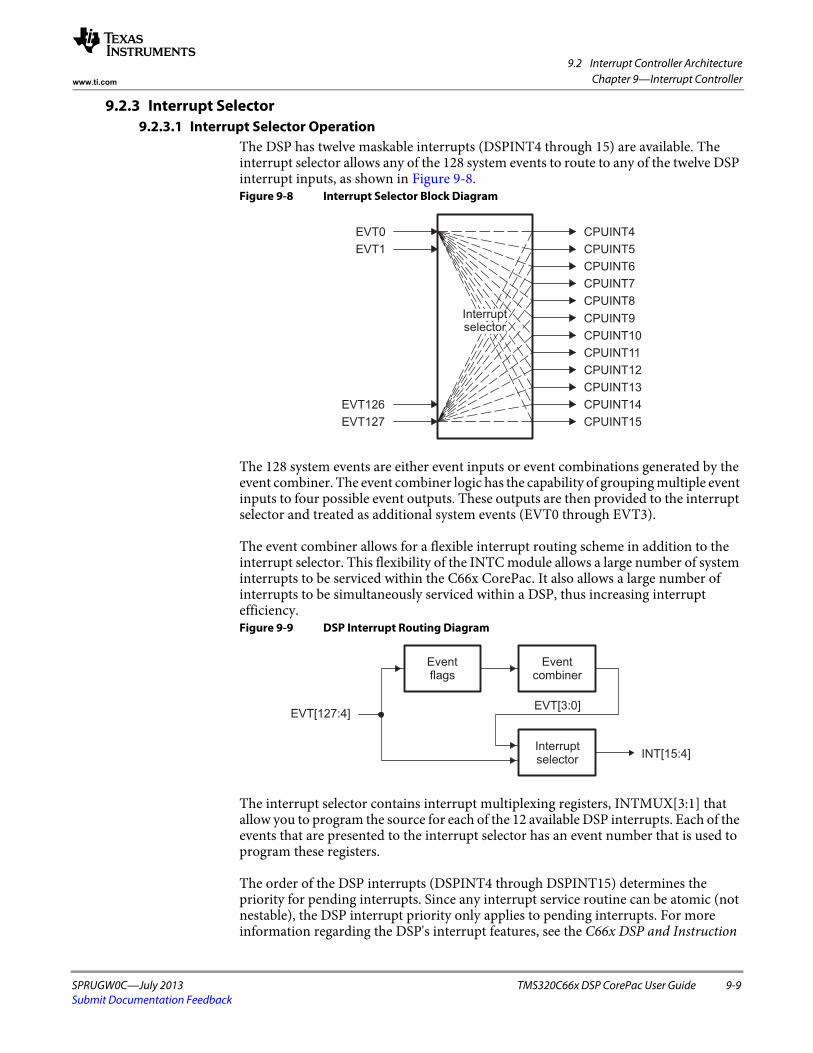
9.2 Interrupt Controller Architecture
SPRUGW0C—July 2013 TMS320C66x DSP CorePac User Guide 9-9Submit Documentation Feedback
Chapter 9—Interrupt Controllerwww.ti.com
9.2.3 Interrupt Selector9.2.3.1 Interrupt Selector Operation
The DSP has twelve maskable interrupts (DSPINT4 through 15) are available. The interrupt selector allows any of the 128 system events to route to any of the twelve DSP interrupt inputs, as shown in Figure 9-8. Figure 9-8 Interrupt Selector Block Diagram
The 128 system events are either event inputs or event combinations generated by the event combiner. The event combiner logic has the capability of grouping multiple event inputs to four possible event outputs. These outputs are then provided to the interrupt selector and treated as additional system events (EVT0 through EVT3).
The event combiner allows for a flexible interrupt routing scheme in addition to the interrupt selector. This flexibility of the INTC module allows a large number of system interrupts to be serviced within the C66x CorePac. It also allows a large number of interrupts to be simultaneously serviced within a DSP, thus increasing interrupt efficiency. Figure 9-9 DSP Interrupt Routing Diagram
The interrupt selector contains interrupt multiplexing registers, INTMUX[3:1] that allow you to program the source for each of the 12 available DSP interrupts. Each of the events that are presented to the interrupt selector has an event number that is used to program these registers.
The order of the DSP interrupts (DSPINT4 through DSPINT15) determines the priority for pending interrupts. Since any interrupt service routine can be atomic (not nestable), the DSP interrupt priority only applies to pending interrupts. For more information regarding the DSP's interrupt features, see the C66x DSP and Instruction
CPUINT4
CPUINT5
CPUINT7
CPUINT6
CPUINT10
CPUINT11
CPUINT9
CPUINT8
CPUINT12
CPUINT13
CPUINT15
CPUINT14
EVT0
EVT1
EVT126
EVT127
Interruptselector
Eventcombiner
EVT[3:0]
selectorInterrupt
flagsEvent
EVT[127:4]
INT[15:4]
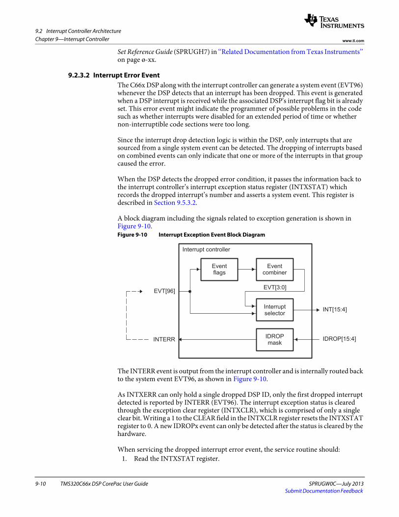
9.2 Interrupt Controller Architecture
9-10 TMS320C66x DSP CorePac User Guide SPRUGW0C—July 2013Submit Documentation Feedback
Chapter 9—Interrupt Controller www.ti.com
Set Reference Guide (SPRUGH7) in ‘‘Related Documentation from Texas Instruments’’ on page ø-xx.
9.2.3.2 Interrupt Error EventThe C66x DSP along with the interrupt controller can generate a system event (EVT96) whenever the DSP detects that an interrupt has been dropped. This event is generated when a DSP interrupt is received while the associated DSP's interrupt flag bit is already set. This error event might indicate the programmer of possible problems in the code such as whether interrupts were disabled for an extended period of time or whether non-interruptible code sections were too long.
Since the interrupt drop detection logic is within the DSP, only interrupts that are sourced from a single system event can be detected. The dropping of interrupts based on combined events can only indicate that one or more of the interrupts in that group caused the error.
When the DSP detects the dropped error condition, it passes the information back to the interrupt controller’s interrupt exception status register (INTXSTAT) which records the dropped interrupt’s number and asserts a system event. This register is described in Section 9.5.3.2.
A block diagram including the signals related to exception generation is shown in Figure 9-10. Figure 9-10 Interrupt Exception Event Block Diagram
The INTERR event is output from the interrupt controller and is internally routed back to the system event EVT96, as shown in Figure 9-10.
As INTXERR can only hold a single dropped DSP ID, only the first dropped interrupt detected is reported by INTERR (EVT96). The interrupt exception status is cleared through the exception clear register (INTXCLR), which is comprised of only a single clear bit. Writing a 1 to the CLEAR field in the INTXCLR register resets the INTXSTAT register to 0. A new IDROPx event can only be detected after the status is cleared by the hardware.
When servicing the dropped interrupt error event, the service routine should:1. Read the INTXSTAT register.
Eventcombiner
EVT[3:0]
selectorInterrupt
flagsEvent
EVT[96]
INT[15:4]
IDROPmask
Interrupt controller
INTERR IDROP[15:4]
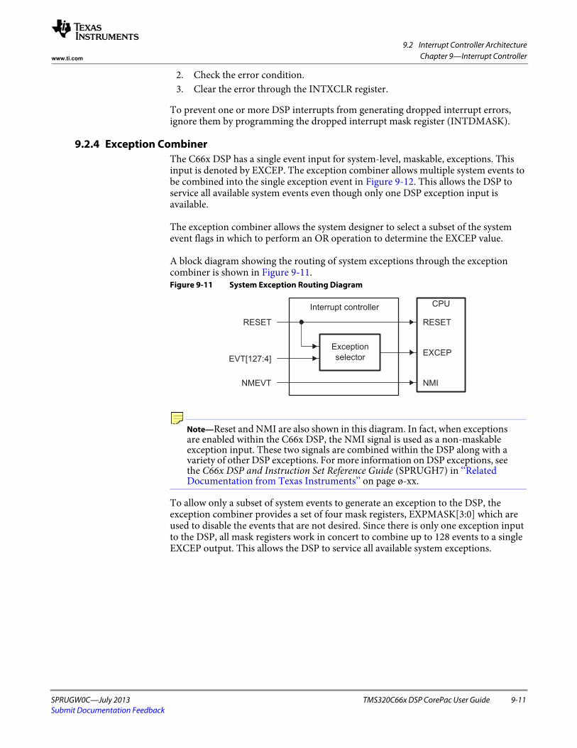
9.2 Interrupt Controller Architecture
SPRUGW0C—July 2013 TMS320C66x DSP CorePac User Guide 9-11Submit Documentation Feedback
Chapter 9—Interrupt Controllerwww.ti.com
2. Check the error condition. 3. Clear the error through the INTXCLR register.
To prevent one or more DSP interrupts from generating dropped interrupt errors, ignore them by programming the dropped interrupt mask register (INTDMASK).
9.2.4 Exception CombinerThe C66x DSP has a single event input for system-level, maskable, exceptions. This input is denoted by EXCEP. The exception combiner allows multiple system events to be combined into the single exception event in Figure 9-12. This allows the DSP to service all available system events even though only one DSP exception input is available.
The exception combiner allows the system designer to select a subset of the system event flags in which to perform an OR operation to determine the EXCEP value.
A block diagram showing the routing of system exceptions through the exception combiner is shown in Figure 9-11. Figure 9-11 System Exception Routing Diagram
Note—Reset and NMI are also shown in this diagram. In fact, when exceptions are enabled within the C66x DSP, the NMI signal is used as a non-maskable exception input. These two signals are combined within the DSP along with a variety of other DSP exceptions. For more information on DSP exceptions, see the C66x DSP and Instruction Set Reference Guide (SPRUGH7) in ‘‘Related Documentation from Texas Instruments’’ on page ø-xx.
To allow only a subset of system events to generate an exception to the DSP, the exception combiner provides a set of four mask registers, EXPMASK[3:0] which are used to disable the events that are not desired. Since there is only one exception input to the DSP, all mask registers work in concert to combine up to 128 events to a single EXCEP output. This allows the DSP to service all available system exceptions.
Exception
selector
RESET
EXCEP
NMI
Interrupt controller CPU
RESET
EVT[127:4]
NMEVT
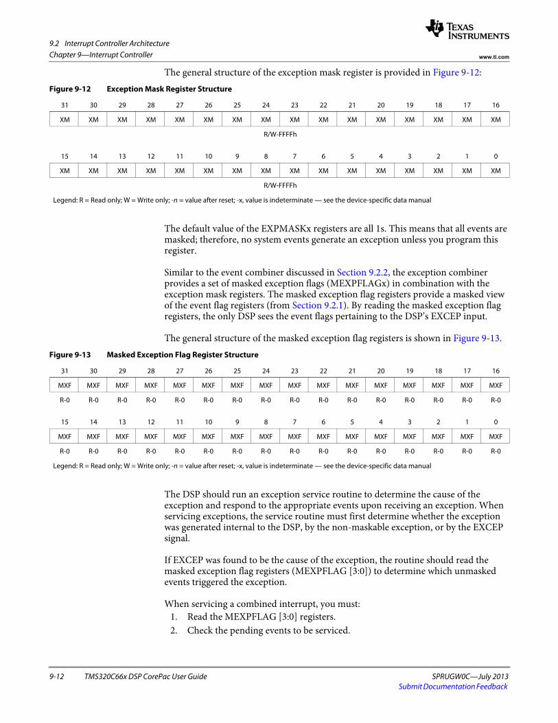
9.2 Interrupt Controller Architecture
9-12 TMS320C66x DSP CorePac User Guide SPRUGW0C—July 2013Submit Documentation Feedback
Chapter 9—Interrupt Controller www.ti.com
The general structure of the exception mask register is provided in Figure 9-12:
The default value of the EXPMASKx registers are all 1s. This means that all events are masked; therefore, no system events generate an exception unless you program this register.
Similar to the event combiner discussed in Section 9.2.2, the exception combiner provides a set of masked exception flags (MEXPFLAGx) in combination with the exception mask registers. The masked exception flag registers provide a masked view of the event flag registers (from Section 9.2.1). By reading the masked exception flag registers, the only DSP sees the event flags pertaining to the DSP’s EXCEP input.
The general structure of the masked exception flag registers is shown in Figure 9-13.
The DSP should run an exception service routine to determine the cause of the exception and respond to the appropriate events upon receiving an exception. When servicing exceptions, the service routine must first determine whether the exception was generated internal to the DSP, by the non-maskable exception, or by the EXCEP signal.
If EXCEP was found to be the cause of the exception, the routine should read the masked exception flag registers (MEXPFLAG [3:0]) to determine which unmasked events triggered the exception.
When servicing a combined interrupt, you must: 1. Read the MEXPFLAG [3:0] registers.2. Check the pending events to be serviced.
Figure 9-12 Exception Mask Register Structure
31 30 29 28 27 26 25 24 23 22 21 20 19 18 17 16
XM XM XM XM XM XM XM XM XM XM XM XM XM XM XM XM
R/W-FFFFh
15 14 13 12 11 10 9 8 7 6 5 4 3 2 1 0
XM XM XM XM XM XM XM XM XM XM XM XM XM XM XM XM
R/W-FFFFh
Legend: R = Read only; W = Write only; -n = value after reset; -x, value is indeterminate — see the device-specific data manual
Figure 9-13 Masked Exception Flag Register Structure
31 30 29 28 27 26 25 24 23 22 21 20 19 18 17 16
MXF MXF MXF MXF MXF MXF MXF MXF MXF MXF MXF MXF MXF MXF MXF MXF
R-0 R-0 R-0 R-0 R-0 R-0 R-0 R-0 R-0 R-0 R-0 R-0 R-0 R-0 R-0 R-0
15 14 13 12 11 10 9 8 7 6 5 4 3 2 1 0
MXF MXF MXF MXF MXF MXF MXF MXF MXF MXF MXF MXF MXF MXF MXF MXF
R-0 R-0 R-0 R-0 R-0 R-0 R-0 R-0 R-0 R-0 R-0 R-0 R-0 R-0 R-0 R-0
Legend: R = Read only; W = Write only; -n = value after reset; -x, value is indeterminate — see the device-specific data manual

9.2 Interrupt Controller Architecture
SPRUGW0C—July 2013 TMS320C66x DSP CorePac User Guide 9-13Submit Documentation Feedback
Chapter 9—Interrupt Controllerwww.ti.com
3. Write the MEXPFLAG [3:0] values to the EVTCLR [3:0] registers. Using the MEXPFLAGx values with the EVTCLRx registers only clears those events that were combined to generate EXCEP. Any events that are masked in EXPMASKx would not need to be cleared, even if set in the EVTFLAGx register; this allows them to be used to generate a combined interrupt event.
4. The DSP should iterate on steps 1 to 3 until no pending events are found before returning from the exception service routine. This ensures that any events received during the exception service routine are captured.
Note—Step 4 is critical if the DSP is required to respond to any new exceptions.
Two facts indicate why this is the case: 1. The output of the exception combiner is active when any unmasked event flag
inputs are active.2. The DSP recognizes an exception request as a 0 to 1 transition.
Therefore, all unmasked event flags must clear before the DSP can recognize a new low to high transition on EXCEP.

9.3 C66x CorePac Events
9-14 TMS320C66x DSP CorePac User Guide SPRUGW0C—July 2013Submit Documentation Feedback
Chapter 9—Interrupt Controller www.ti.com
9.3 C66x CorePac EventsThere are a number of events that the various components of the C66x CorePac generates. These events are routed to the interrupt controller so that when asserted, they can be serviced by the DSP. These events are listed in Table 9-2, along with their event mapping.
Note—The events that are shown as available events are to the C66x CorePac for chip-level events. Therefore, each new C66x device can use these event inputs as necessary. See the device-specific data manual for more information about how these available events are used.
Table 9-2 System Event Mapping
EVT Number Event From Description
0 EVT0 INT controller Output of event combiner 0, for events 1 through 31.
1 EVT1 INT controller Output of event combiner 1, for events 32 through 63.
2 EVT2 INT controller Output of event combiner 2, for events 64 through 95.
3 EVT3 INT controller Output of event combiner 3, for events 96 through 127.
4-8 Available events.
9 Reserved
10 Available events.
11-12 Reserved
13 IDMAINT0 EMC IDMA channel 0 interrupt
14 IDMAINT1 EMC IDMA channel 1 interrupt
15-95 Available events.
96 INTERR INT controller Dropped DSP interrupt event
97 EMC_IDMAERR EMC Invalid IDMA parameters
98 Reserved
99 Available events.
100-101 Reserved
102-109 Available events.
110 MDMAERREVT L2 MDMA bus error event
111 Reserved
112 Available events.
113 L1P_ED L1P Single bit error detected during DMA read
114-115 Available events.
116 L2_ED1 L2 Corrected bit error detected
117 L2_ED2 L2 Uncorrected bit error detected
118 PDC_INT PDC PDC sleep interrupt
119 SYS_CMPA SYS DSP memory protection fault
120 L1P_CMPA L1P DSP memory protection fault
121 L1P_DMPA L1P DMA memory protection fault
122 L1D_CMPA L1D DSP memory protection fault
123 L1D_DMPA L1D DMA memory protection fault
124 L2_CMPA L2 DSP memory protection fault
125 L2_DMPA L2 DMA memory protection fault
126 EMC_CMPA EMC DSP memory protection fault
127 EMC_BUSERR EMC CFG bus error event

9.4 Interrupt Controller - DSP Interaction
SPRUGW0C—July 2013 TMS320C66x DSP CorePac User Guide 9-15Submit Documentation Feedback
Chapter 9—Interrupt Controllerwww.ti.com
9.4 Interrupt Controller - DSP Interaction9.4.1 DSP - Interrupt Controller Interface
The interrupt controller’s outputs, as produced by the exception combiner and the interrupt selector, are provided to the C66x DSP.
The twelve interrupt signals are reflected in the DSP’s interrupt flag register (IFR), as shown in Figure 9-14.
Figure 9-14 DSP Event Routing Diagram
You must enable interrupts in order for the DSP to recognize them. The DSP requires individual enables via the interrupt enable register (IER) and via the global interrupt enable field in the interrupt task register (ITSR.GIE).
Also note that the exception signal (EXCEP) is recorded in the DSP’s exception flag register (EFR) in Figure 9-15. You must enable exception before the exception flag registers (EFR) shown can be recognized. Exception recognition is disabled after device reset for ease of system design and for backward compatibility. You can turn on exceptions by setting the global exceptions enable field (GEE) in the ITSR register (ITSR). You should enable exceptions prior to enabling any interrupts to ensure that an NMI is not received while its mode (exception vs. interrupt) is changing.
When system exceptions are not enabled in the DSP, the non-maskable interrupt (NMI) acts as an interrupt and when received will post a flag to the BIT1 field in the IFR register. When system exceptions are enabled in the DSP; however, this flag is not set. Rather, the exception source is identified in the exception flag register (EFR) to denote whether the source is NMI, EXCEP, an internal exception, or a software exception (SWE/SWENR).
IF15 14
IF13IF IF
12 11IF IF
10 8IFIF
9 6IFIF
7IF5
IF4
Reserved
31 16 15 14 13 12 11 10 9 8 7 6 5 4 3 2 1 0
IF3 1
IFIF2
IF0
INT4
INT5
INT6
INT7
INT8
INT9
INT10
INT11
INT12
INT13
INT14
INT15
NXF EXF IXF SXF
31 30 29 2 1 0
Reserved
Interruptselector
Eventcombinerflags
Event
NMI
combinerException Software excep
Internalexcep
EFR
EXCEP
IFR
CPU
NMEVT
EVT4
EVT5
EVT6
EVT126
EVT127

9.4 Interrupt Controller - DSP Interaction
9-16 TMS320C66x DSP CorePac User Guide SPRUGW0C—July 2013Submit Documentation Feedback
Chapter 9—Interrupt Controller www.ti.com
All NMI processing shares the NMI interrupt vector, regardless of whether you are using it as an interrupt or it represents an exception. The DSP only uses its REP register as a vector as opposed to the NMI vector in the case where the SWENR generates an exception rather than SWE instruction.
For more detailed information, see the C66x DSP and Instruction Set Reference Guide (SPRUGH7) in ‘‘Related Documentation from Texas Instruments’’ on page ø-xx.
9.4.2 DSP Servicing of Interrupt EventsFor the case where the DSP services single-event interrupts (where system events are specified directly in the Interrupt Selector), there is no need to read or clear the Event Flag (EVTFLAGx) registers in the Interrupt Controller.
However, you must use event flags within an interrupt service routine or an exception service routine when servicing combined system events. These flags are used to determine the event(s) that initiated an interrupt or exception. In other words, the DSP’s interrupt flag register (or exception flag register) tell the DSP a combined event has occurred, then the service routine must use the event flag register to determine the exact cause(s).
It is also important to note that within the service routine, the appropriate event flag register bits must be cleared by software in order to receive a subsequent event. If the event flag(s) does not clear, then a new system event will not be recognized. The new system event cannot be recognized as a dropped interrupt. This is because the DSP dropped interrupt logic applies to the DSP interrupt input (not the interrupt controller event input). Since the events are combined in the Interrupt Controller, the DSP has no visibility here.
In many systems, it may be tempting to have the service routine read, then clear the entire event flag register (EVTFLAGx). While this can work fine for some systems, you must take care that some of the event flags are not being polled by any of the system’s code. If a particular event must be polled (read occasionally by some code within the system rather than allowing that event to interrupt the DSP), then indiscriminately clearing all of the event flag bits may cause unexpected results.
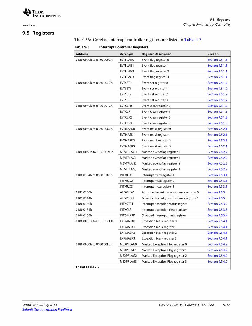
9.5 Registers
SPRUGW0C—July 2013 TMS320C66x DSP CorePac User Guide 9-17Submit Documentation Feedback
Chapter 9—Interrupt Controllerwww.ti.com
9.5 RegistersThe C66x CorePac interrupt controller registers are listed in Table 9-3.Table 9-3 Interrupt Controller Registers
Address Acronym Register Description Section
0180 0000h to 0180 000Ch EVTFLAG0 Event flag register 0 Section 9.5.1.1
EVTFLAG1 Event flag register 1 Section 9.5.1.1
EVTFLAG2 Event flag register 2 Section 9.5.1.1
EVTFLAG3 Event flag register 3 Section 9.5.1.1
0180 0020h to 0180 002Ch EVTSET0 Event set register 0 Section 9.5.1.2
EVTSET1 Event set register 1 Section 9.5.1.2
EVTSET2 Event set register 2 Section 9.5.1.2
EVTSET3 Event set register 3 Section 9.5.1.2
0180 0040h to 0180 004Ch EVTCLR0 Event clear register 0 Section 9.5.1.3
EVTCLR1 Event clear register 1 Section 9.5.1.3
EVTCLR2 Event clear register 2 Section 9.5.1.3
EVTCLR3 Event clear register 3 Section 9.5.1.3
0180 0080h to 0180 008Ch EVTMASK0 Event mask register 0 Section 9.5.2.1
EVTMASK1 Event mask register 1 Section 9.5.2.1
EVTMASK2 Event mask register 2 Section 9.5.2.1
EVTMASK3 Event mask register 3 Section 9.5.2.1
0180 00A0h to 0180 00ACh MEVTFLAG0 Masked event flag register 0 Section 9.5.2.2
MEVTFLAG1 Masked event flag register 1 Section 9.5.2.2
MEVTFLAG2 Masked event flag register 2 Section 9.5.2.2
MEVTFLAG3 Masked event flag register 3 Section 9.5.2.2
0180 0104h to 0180 010Ch INTMUX1 Interrupt mux register 1 Section 9.5.3.1
INTMUX2 Interrupt mux register 2 Section 9.5.3.1
INTMUX3 Interrupt mux register 3 Section 9.5.3.1
0181 0140h AEGMUX0 Advanced event generator mux register 0 Section 9.5.5
0181 0144h AEGMUX1 Advanced event generator mux register 1 Section 9.5.5
0180 0180h INTXSTAT Interrupt exception status register Section 9.5.3.2
0180 0184h INTXCLR Interrupt exception clear register Section 9.5.3.3
0180 0188h INTDMASK Dropped interrupt mask register Section 9.5.3.4
0180 00C0h to 0180 00CCh EXPMASK0 Exception Mask register 0 Section 9.5.4.1
EXPMASK1 Exception Mask register 1 Section 9.5.4.1
EXPMASK2 Exception Mask register 2 Section 9.5.4.1
EXPMASK3 Exception Mask register 3 Section 9.5.4.1
0180 00E0h to 0180 00ECh MEXPFLAG0 Masked Exception Flag register 0 Section 9.5.4.2
MEXPFLAG1 Masked Exception Flag register 1 Section 9.5.4.2
MEXPFLAG2 Masked Exception Flag register 2 Section 9.5.4.2
MEXPFLAG3 Masked Exception Flag register 3 Section 9.5.4.2
End of Table 9-3
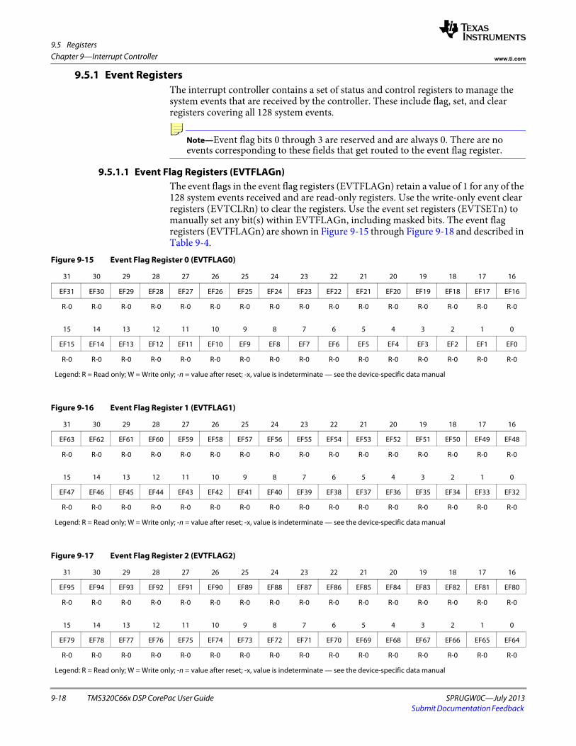
9.5 Registers
9-18 TMS320C66x DSP CorePac User Guide SPRUGW0C—July 2013Submit Documentation Feedback
Chapter 9—Interrupt Controller www.ti.com
9.5.1 Event RegistersThe interrupt controller contains a set of status and control registers to manage the system events that are received by the controller. These include flag, set, and clear registers covering all 128 system events.
Note—Event flag bits 0 through 3 are reserved and are always 0. There are no events corresponding to these fields that get routed to the event flag register.
9.5.1.1 Event Flag Registers (EVTFLAGn) The event flags in the event flag registers (EVTFLAGn) retain a value of 1 for any of the 128 system events received and are read-only registers. Use the write-only event clear registers (EVTCLRn) to clear the registers. Use the event set registers (EVTSETn) to manually set any bit(s) within EVTFLAGn, including masked bits. The event flag registers (EVTFLAGn) are shown in Figure 9-15 through Figure 9-18 and described in Table 9-4.
Figure 9-15 Event Flag Register 0 (EVTFLAG0)
31 30 29 28 27 26 25 24 23 22 21 20 19 18 17 16
EF31 EF30 EF29 EF28 EF27 EF26 EF25 EF24 EF23 EF22 EF21 EF20 EF19 EF18 EF17 EF16
R-0 R-0 R-0 R-0 R-0 R-0 R-0 R-0 R-0 R-0 R-0 R-0 R-0 R-0 R-0 R-0
15 14 13 12 11 10 9 8 7 6 5 4 3 2 1 0
EF15 EF14 EF13 EF12 EF11 EF10 EF9 EF8 EF7 EF6 EF5 EF4 EF3 EF2 EF1 EF0
R-0 R-0 R-0 R-0 R-0 R-0 R-0 R-0 R-0 R-0 R-0 R-0 R-0 R-0 R-0 R-0
Legend: R = Read only; W = Write only; -n = value after reset; -x, value is indeterminate — see the device-specific data manual
Figure 9-16 Event Flag Register 1 (EVTFLAG1)
31 30 29 28 27 26 25 24 23 22 21 20 19 18 17 16
EF63 EF62 EF61 EF60 EF59 EF58 EF57 EF56 EF55 EF54 EF53 EF52 EF51 EF50 EF49 EF48
R-0 R-0 R-0 R-0 R-0 R-0 R-0 R-0 R-0 R-0 R-0 R-0 R-0 R-0 R-0 R-0
15 14 13 12 11 10 9 8 7 6 5 4 3 2 1 0
EF47 EF46 EF45 EF44 EF43 EF42 EF41 EF40 EF39 EF38 EF37 EF36 EF35 EF34 EF33 EF32
R-0 R-0 R-0 R-0 R-0 R-0 R-0 R-0 R-0 R-0 R-0 R-0 R-0 R-0 R-0 R-0
Legend: R = Read only; W = Write only; -n = value after reset; -x, value is indeterminate — see the device-specific data manual
Figure 9-17 Event Flag Register 2 (EVTFLAG2)
31 30 29 28 27 26 25 24 23 22 21 20 19 18 17 16
EF95 EF94 EF93 EF92 EF91 EF90 EF89 EF88 EF87 EF86 EF85 EF84 EF83 EF82 EF81 EF80
R-0 R-0 R-0 R-0 R-0 R-0 R-0 R-0 R-0 R-0 R-0 R-0 R-0 R-0 R-0 R-0
15 14 13 12 11 10 9 8 7 6 5 4 3 2 1 0
EF79 EF78 EF77 EF76 EF75 EF74 EF73 EF72 EF71 EF70 EF69 EF68 EF67 EF66 EF65 EF64
R-0 R-0 R-0 R-0 R-0 R-0 R-0 R-0 R-0 R-0 R-0 R-0 R-0 R-0 R-0 R-0
Legend: R = Read only; W = Write only; -n = value after reset; -x, value is indeterminate — see the device-specific data manual
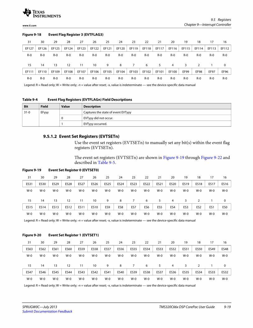
9.5 Registers
SPRUGW0C—July 2013 TMS320C66x DSP CorePac User Guide 9-19Submit Documentation Feedback
Chapter 9—Interrupt Controllerwww.ti.com
9.5.1.2 Event Set Registers (EVTSETn)Use the event set registers (EVTSETn) to manually set any bit(s) within the event flag registers (EVTSETn).
The event set registers (EVTSETn) are shown in Figure 9-19 through Figure 9-22 and described in Table 9-5.
Figure 9-18 Event Flag Register 3 (EVTFLAG3)
31 30 29 28 27 26 25 24 23 22 21 20 19 18 17 16
EF127 EF126 EF125 EF124 EF123 EF122 EF121 EF120 EF119 EF118 EF117 EF116 EF115 EF114 EF113 EF112
R-0 R-0 R-0 R-0 R-0 R-0 R-0 R-0 R-0 R-0 R-0 R-0 R-0 R-0 R-0 R-0
15 14 13 12 11 10 9 8 7 6 5 4 3 2 1 0
EF111 EF110 EF109 EF108 EF107 EF106 EF105 EF104 EF103 EF102 EF101 EF100 EF99 EF98 EF97 EF96
R-0 R-0 R-0 R-0 R-0 R-0 R-0 R-0 R-0 R-0 R-0 R-0 R-0 R-0 R-0 R-0
Legend: R = Read only; W = Write only; -n = value after reset; -x, value is indeterminate — see the device-specific data manual
Table 9-4 Event Flag Registers (EVTFLAGn) Field Descriptions
Bit Field Value Description
31-0 EFyyy Captures the state of event EVTyyy
0 EVTyyy did not occur.
1 EVTyyy occurred.
Figure 9-19 Event Set Register 0 (EVTSET0)
31 30 29 28 27 26 25 24 23 22 21 20 19 18 17 16
ES31 ES30 ES29 ES28 ES27 ES26 ES25 ES24 ES23 ES22 ES21 ES20 ES19 ES18 ES17 ES16
W-0 W-0 W-0 W-0 W-0 W-0 W-0 W-0 W-0 W-0 W-0 W-0 W-0 W-0 W-0 W-0
15 14 13 12 11 10 9 8 7 6 5 4 3 2 1 0
ES15 ES14 ES13 ES12 ES11 ES10 ES9 ES8 ES7 ES6 ES5 ES4 ES3 ES2 ES1 ES0
W-0 W-0 W-0 W-0 W-0 W-0 W-0 W-0 W-0 W-0 W-0 W-0 W-0 W-0 W-0 W-0
Legend: R = Read only; W = Write only; -n = value after reset; -x, value is indeterminate — see the device-specific data manual
Figure 9-20 Event Set Register 1 (EVTSET1)
31 30 29 28 27 26 25 24 23 22 21 20 19 18 17 16
ES63 ES62 ES61 ES60 ES59 ES58 ES57 ES56 ES55 ES54 ES53 ES52 ES51 ES50 ES49 ES48
W-0 W-0 W-0 W-0 W-0 W-0 W-0 W-0 W-0 W-0 W-0 W-0 W-0 W-0 W-0 W-0
15 14 13 12 11 10 9 8 7 6 5 4 3 2 1 0
ES47 ES46 ES45 ES44 ES43 ES42 ES41 ES40 ES39 ES38 ES37 ES36 ES35 ES34 ES33 ES32
W-0 W-0 W-0 W-0 W-0 W-0 W-0 W-0 W-0 W-0 W-0 W-0 W-0 W-0 W-0 W-0
Legend: R = Read only; W = Write only; -n = value after reset; -x, value is indeterminate — see the device-specific data manual
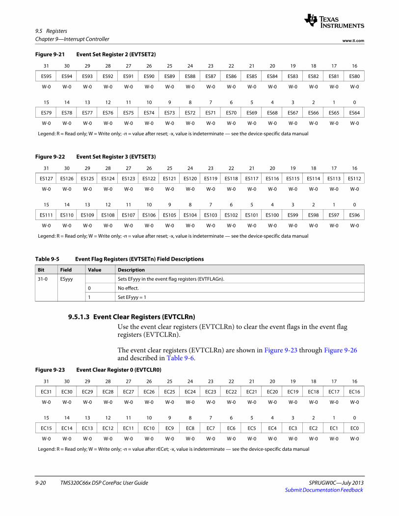
9.5 Registers
9-20 TMS320C66x DSP CorePac User Guide SPRUGW0C—July 2013Submit Documentation Feedback
Chapter 9—Interrupt Controller www.ti.com
9.5.1.3 Event Clear Registers (EVTCLRn)Use the event clear registers (EVTCLRn) to clear the event flags in the event flag registers (EVTCLRn).
The event clear registers (EVTCLRn) are shown in Figure 9-23 through Figure 9-26 and described in Table 9-6.
Figure 9-21 Event Set Register 2 (EVTSET2)
31 30 29 28 27 26 25 24 23 22 21 20 19 18 17 16
ES95 ES94 ES93 ES92 ES91 ES90 ES89 ES88 ES87 ES86 ES85 ES84 ES83 ES82 ES81 ES80
W-0 W-0 W-0 W-0 W-0 W-0 W-0 W-0 W-0 W-0 W-0 W-0 W-0 W-0 W-0 W-0
15 14 13 12 11 10 9 8 7 6 5 4 3 2 1 0
ES79 ES78 ES77 ES76 ES75 ES74 ES73 ES72 ES71 ES70 ES69 ES68 ES67 ES66 ES65 ES64
W-0 W-0 W-0 W-0 W-0 W-0 W-0 W-0 W-0 W-0 W-0 W-0 W-0 W-0 W-0 W-0
Legend: R = Read only; W = Write only; -n = value after reset; -x, value is indeterminate — see the device-specific data manual
Figure 9-22 Event Set Register 3 (EVTSET3)
31 30 29 28 27 26 25 24 23 22 21 20 19 18 17 16
ES127 ES126 ES125 ES124 ES123 ES122 ES121 ES120 ES119 ES118 ES117 ES116 ES115 ES114 ES113 ES112
W-0 W-0 W-0 W-0 W-0 W-0 W-0 W-0 W-0 W-0 W-0 W-0 W-0 W-0 W-0 W-0
15 14 13 12 11 10 9 8 7 6 5 4 3 2 1 0
ES111 ES110 ES109 ES108 ES107 ES106 ES105 ES104 ES103 ES102 ES101 ES100 ES99 ES98 ES97 ES96
W-0 W-0 W-0 W-0 W-0 W-0 W-0 W-0 W-0 W-0 W-0 W-0 W-0 W-0 W-0 W-0
Legend: R = Read only; W = Write only; -n = value after reset; -x, value is indeterminate — see the device-specific data manual
Table 9-5 Event Flag Registers (EVTSETn) Field Descriptions
Bit Field Value Description
31-0 ESyyy Sets EFyyy in the event flag registers (EVTFLAGn).
0 No effect.
1 Set EFyyy = 1
Figure 9-23 Event Clear Register 0 (EVTCLR0)
31 30 29 28 27 26 25 24 23 22 21 20 19 18 17 16
EC31 EC30 EC29 EC28 EC27 EC26 EC25 EC24 EC23 EC22 EC21 EC20 EC19 EC18 EC17 EC16
W-0 W-0 W-0 W-0 W-0 W-0 W-0 W-0 W-0 W-0 W-0 W-0 W-0 W-0 W-0 W-0
15 14 13 12 11 10 9 8 7 6 5 4 3 2 1 0
EC15 EC14 EC13 EC12 EC11 EC10 EC9 EC8 EC7 EC6 EC5 EC4 EC3 EC2 EC1 EC0
W-0 W-0 W-0 W-0 W-0 W-0 W-0 W-0 W-0 W-0 W-0 W-0 W-0 W-0 W-0 W-0
Legend: R = Read only; W = Write only; -n = value after rECet; -x, value is indeterminate — see the device-specific data manual

9.5 Registers
SPRUGW0C—July 2013 TMS320C66x DSP CorePac User Guide 9-21Submit Documentation Feedback
Chapter 9—Interrupt Controllerwww.ti.com
9.5.2 Event Combiner RegistersThere are a set of event mask registers (EVTMASK [3:0]) to program the event combiner. These registers allow up to 32 events to be combined into a single combined event which can then be used by the interrupt selector. The event mask bits within the EVTMASK [3:0] registers act to mask (or enable) the received system events. There are four event signals presented to the interrupt selector (EVT [3:0]).
Figure 9-24 Event Clear Register 1 (EVTCLR1)
31 30 29 28 27 26 25 24 23 22 21 20 19 18 17 16
EC63 EC62 EC61 EC60 EC59 EC58 EC57 EC56 EC55 EC54 EC53 EC52 EC51 EC50 EC49 EC48
W-0 W-0 W-0 W-0 W-0 W-0 W-0 W-0 W-0 W-0 W-0 W-0 W-0 W-0 W-0 W-0
15 14 13 12 11 10 9 8 7 6 5 4 3 2 1 0
EC47 EC46 EC45 EC44 EC43 EC42 EC41 EC40 EC39 EC38 EC37 EC36 EC35 EC34 EC33 EC32
W-0 W-0 W-0 W-0 W-0 W-0 W-0 W-0 W-0 W-0 W-0 W-0 W-0 W-0 W-0 W-0
Legend: R = Read only; W = Write only; -n = value after reset; -x, value is indeterminate — see the device-specific data manual
Figure 9-25 Event Clear Register 2 (EVTCLR2)
31 30 29 28 27 26 25 24 23 22 21 20 19 18 17 16
EC95 EC94 EC93 EC92 EC91 EC90 EC89 EC88 EC87 EC86 EC85 EC84 EC83 EC82 EC81 EC80
W-0 W-0 W-0 W-0 W-0 W-0 W-0 W-0 W-0 W-0 W-0 W-0 W-0 W-0 W-0 W-0
15 14 13 12 11 10 9 8 7 6 5 4 3 2 1 0
EC79 EC78 EC77 EC76 EC75 EC74 EC73 EC72 EC71 EC70 EC69 EC68 EC67 EC66 EC65 EC64
W-0 W-0 W-0 W-0 W-0 W-0 W-0 W-0 W-0 W-0 W-0 W-0 W-0 W-0 W-0 W-0
Legend: R = Read only; W = Write only; -n = value after reset; -x, value is indeterminate — see the device-specific data manual
Figure 9-26 Event Clear Register 3 (EVTCLR3)
31 30 29 28 27 26 25 24 23 22 21 20 19 18 17 16
EC127 EC126 EC125 EC124 EC123 EC122 EC121 EC120 EC119 EC118 EC117 EC116 EC115 EC114 EC113 EC112
W-0 W-0 W-0 W-0 W-0 W-0 W-0 W-0 W-0 W-0 W-0 W-0 W-0 W-0 W-0 W-0
15 14 13 12 11 10 9 8 7 6 5 4 3 2 1 0
EC111 EC110 EC109 EC108 EC107 EC106 EC105 EC104 EC103 EC102 EC101 EC100 EC99 EC98 EC97 EC96
W-0 W-0 W-0 W-0 W-0 W-0 W-0 W-0 W-0 W-0 W-0 W-0 W-0 W-0 W-0 W-0
Legend: R = Read only; W = Write only; -n = value after reset; -x, value is indeterminate — see the device-specific data manual
Table 9-6 Event Flag Registers (EVTCLRn) Field Descriptions
Bit Field Value Description
31-0 ECyyy Clears EFyyy in the event flag registers (EVTFLAGn).
0 No effect.
1 Set EFyyy = 0.

9.5 Registers
9-22 TMS320C66x DSP CorePac User Guide SPRUGW0C—July 2013Submit Documentation Feedback
Chapter 9—Interrupt Controller www.ti.com
The event mask registers are shown below (Bits EM [3:0] are unused).
9.5.2.1 Event Mask Registers (EVTMASKn) There are a set of event mask registers (EVTMASK0 through EVTMASK3) to program the event combiner. These registers allow up to 32 events to be combined into a single event output that is used as a single DSP interrupt or AET event. The event mask bits within the EVTMASKn register act as enablers for the received system events to be combined on the event outputs. There are four event outputs to the event and AET event selectors (EVT [3:0]).
The event mask registers (EVTMASKn) are shown in Figure 9-27 through Figure 9-30 and described in Table 9-7.
Figure 9-27 Event Mask Register 0 (EVTMASK0)
31 30 29 28 27 26 25 24 23 22 21 20 19 18 17 16
EM31 EM30 EM29 EM28 EM27 EM26 EM25 EM24 EM23 EM22 EM21 EM20 EM19 EM18 EM17 EM16
R/W-0 R/W-0 R/W-0 R/W-0 R/W-0 R/W-0 R/W-0 R/W-0 R/W-0 R/W-0 R/W-0 R/W-0 R/W-0 R/W-0 R/W-0 R/W-0
15 14 13 12 11 10 9 8 7 6 5 4 3 2 1 0
EM15 EM14 EM13 EM12 EM11 EM10 EM9 EM8 EM7 EM6 EM5 EM4 EM3 EM2 EM1 EM0
R/W-0 R/W-0 R/W-0 R/W-0 R/W-0 R/W-0 R/W-0 R/W-0 R/W-0 R/W-0 R/W-0 R/W-0 R-1 R-1 R-1 R-1
Legend: R = Read only; W = Write only; -n = value after rECet; -x, value is indeterminate — see the device-specific data manual
Figure 9-28 Event Mask Register 1 (EVTMASK1)
31 30 29 28 27 26 25 24 23 22 21 20 19 18 17 16
EM63 EM62 EM61 EM60 EM59 EM58 EM57 EM56 EM55 EM54 EM53 EM52 EM51 EM50 EM49 EM48
R/W-0 R/W-0 R/W-0 R/W-0 R/W-0 R/W-0 R/W-0 R/W-0 R/W-0 R/W-0 R/W-0 R/W-0 R/W-0 R/W-0 R/W-0 R/W-0
15 14 13 12 11 10 9 8 7 6 5 4 3 2 1 0
EM47 EM46 EM45 EM44 EM43 EM42 EM41 EM40 EM39 EM38 EM37 EM36 EM35 EM34 EM33 EM32
R/W-0 R/W-0 R/W-0 R/W-0 R/W-0 R/W-0 R/W-0 R/W-0 R/W-0 R/W-0 R/W-0 R/W-0 R/W-0 R/W-0 R/W-0 R/W-0
Legend: R = Read only; W = Write only; -n = value after reset; -x, value is indeterminate — see the device-specific data manual
Figure 9-29 Event Mask Register 2 (EVTMASK2)
31 30 29 28 27 26 25 24 23 22 21 20 19 18 17 16
EM95 EM94 EM93 EM92 EM91 EM90 EM89 EM88 EM87 EM86 EM85 EM84 EM83 EM82 EM81 EM80
R/W-0 R/W-0 R/W-0 R/W-0 R/W-0 R/W-0 R/W-0 R/W-0 R/W-0 R/W-0 R/W-0 R/W-0 R/W-0 R/W-0 R/W-0 R/W-0
15 14 13 12 11 10 9 8 7 6 5 4 3 2 1 0
EM79 EM78 EM77 EM76 EM75 EM74 EM73 EM72 EM71 EM70 EM69 EM68 EM67 EM66 EM65 EM64
R/W-0 R/W-0 R/W-0 R/W-0 R/W-0 R/W-0 R/W-0 R/W-0 R/W-0 R/W-0 R/W-0 R/W-0 R/W-0 R/W-0 R/W-0 R/W-0
Legend: R = Read only; W = Write only; -n = value after reset; -x, value is indeterminate — see the device-specific data manual
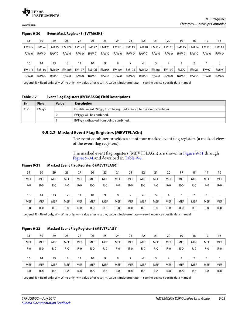
9.5 Registers
SPRUGW0C—July 2013 TMS320C66x DSP CorePac User Guide 9-23Submit Documentation Feedback
Chapter 9—Interrupt Controllerwww.ti.com
9.5.2.2 Masked Event Flag Registers (MEVTFLAGn)The event combiner provides a set of four masked event flag registers (a masked view of the event flag registers).
The masked event flag registers (MEVTFLAGn) are shown in Figure 9-31 through Figure 9-34 and described in Table 9-8.
Figure 9-30 Event Mask Register 3 (EVTMASK3)
31 30 29 28 27 26 25 24 23 22 21 20 19 18 17 16
EM127 EM126 EM125 EM124 EM123 EM122 EM121 EM120 EM119 EM118 EM117 EM116 EM115 EM114 EM113 EM112
R/W-0 R/W-0 R/W-0 R/W-0 R/W-0 R/W-0 R/W-0 R/W-0 R/W-0 R/W-0 R/W-0 R/W-0 R/W-0 R/W-0 R/W-0 R/W-0
15 14 13 12 11 10 9 8 7 6 5 4 3 2 1 0
EM111 EM110 EM109 EM108 EM107 EM106 EM105 EM104 EM103 EM102 EM101 EM100 EM99 EM98 EM97 EM96
R/W-0 R/W-0 R/W-0 R/W-0 R/W-0 R/W-0 R/W-0 R/W-0 R/W-0 R/W-0 R/W-0 R/W-0 R/W-0 R/W-0 R/W-0 R/W-0
Legend: R = Read only; W = Write only; -n = value after reset; -x, value is indeterminate — see the device-specific data manual
Table 9-7 Event Flag Registers (EVTMASKn) Field Descriptions
Bit Field Value Description
31-0 EMyyy Disables event EVTyyy from being used as input to the event combiner.
0 EVTyyy will be combined.
1 EVTyyy is disabled from being combined.
Figure 9-31 Masked Event Flag Register 0 (MEVTFLAG0)
31 30 29 28 27 26 25 24 23 22 21 20 19 18 17 16
MEF MEF MEF MEF MEF MEF MEF MEF MEF MEF MEF MEF MEF MEF MEF MEF
R-0 R-0 R-0 R-0 R-0 R-0 R-0 R-0 R-0 R-0 R-0 R-0 R-0 R-0 R-0 R-0
15 14 13 12 11 10 9 8 7 6 5 4 3 2 1 0
MEF MEF MEF MEF MEF MEF MEF MEF MEF MEF MEF MEF MEF MEF MEF MEF
R-0 R-0 R-0 R-0 R-0 R-0 R-0 R-0 R-0 R-0 R-0 R-0 R-0 R-0 R-0 R-0
Legend: R = Read only; W = Write only; -n = value after reset; -x, value is indeterminate — see the device-specific data manual
Figure 9-32 Masked Event Flag Register 1 (MEVTFLAG1)
31 30 29 28 27 26 25 24 23 22 21 20 19 18 17 16
MEF MEF MEF MEF MEF MEF MEF MEF MEF MEF MEF MEF MEF MEF MEF MEF
R-0 R-0 R-0 R-0 R-0 R-0 R-0 R-0 R-0 R-0 R-0 R-0 R-0 R-0 R-0 R-0
15 14 13 12 11 10 9 8 7 6 5 4 3 2 1 0
MEF MEF MEF MEF MEF MEF MEF MEF MEF MEF MEF MEF MEF MEF MEF MEF
R-0 R-0 R-0 R-0 R-0 R-0 R-0 R-0 R-0 R-0 R-0 R-0 R-0 R-0 R-0 R-0
Legend: R = Read only; W = Write only; -n = value after reset; -x, value is indeterminate — see the device-specific data manual

9.5 Registers
9-24 TMS320C66x DSP CorePac User Guide SPRUGW0C—July 2013Submit Documentation Feedback
Chapter 9—Interrupt Controller www.ti.com
Figure 9-33 Masked Event Flag Register 2 (MEVTFLAG2)
31 30 29 28 27 26 25 24 23 22 21 20 19 18 17 16
MEF MEF MEF MEF MEF MEF MEF MEF MEF MEF MEF MEF MEF MEF MEF MEF
R-0 R-0 R-0 R-0 R-0 R-0 R-0 R-0 R-0 R-0 R-0 R-0 R-0 R-0 R-0 R-0
15 14 13 12 11 10 9 8 7 6 5 4 3 2 1 0
MEF MEF MEF MEF MEF MEF MEF MEF MEF MEF MEF MEF MEF MEF MEF MEF
R-0 R-0 R-0 R-0 R-0 R-0 R-0 R-0 R-0 R-0 R-0 R-0 R-0 R-0 R-0 R-0
Legend: R = Read only; W = Write only; -n = value after reset; -x, value is indeterminate — see the device-specific data manual
Figure 9-34 Masked Event Flag Register 3 (MEVTFLAG3)
31 30 29 28 27 26 25 24 23 22 21 20 19 18 17 16
MEF MEF MEF MEF MEF MEF MEF MEF MEF MEF MEF MEF MEF MEF MEF MEF
R-0 R-0 R-0 R-0 R-0 R-0 R-0 R-0 R-0 R-0 R-0 R-0 R-0 R-0 R-0 R-0
15 14 13 12 11 10 9 8 7 6 5 4 3 2 1 0
MEF MEF MEF MEF MEF MEF MEF MEF MEF MEF MEF MEF MEF MEF MEF MEF
R-0 R-0 R-0 R-0 R-0 R-0 R-0 R-0 R-0 R-0 R-0 R-0 R-0 R-0 R-0 R-0
Legend: R = Read only; W = Write only; -n = value after reset; -x, value is indeterminate — see the device-specific data manual
Table 9-8 Masked Event Flag Registers (MEVTFLAGn) Field Descriptions
Bit Field Value Description
31-0 MEFyyy 0-FFFF FFFFh Displays content of EFyyy when EMyyy = 0 in the event mask registers (EVTMASKn).
If (EMyyy = 0) MEFyyy = EFyyy ElseMEFyyy = 0

9.5 Registers
SPRUGW0C—July 2013 TMS320C66x DSP CorePac User Guide 9-25Submit Documentation Feedback
Chapter 9—Interrupt Controllerwww.ti.com
9.5.3 DSP Interrupt Selector Registers9.5.3.1 Interrupt Mux Registers (INTMUXn)
The interrupt selector contains interrupt mux registers that allow you to program the source for each of the 12 available DSP interrupts.
The interrupt mux registers are shown in Figure 9-35 through Figure 9-37 and described in Table 9-9.
Figure 9-35 Interrupt Mux Register 1 (INTMUX1)
31 30 24 23 22 16
Reserved INTSEL7 Reserved INTSEL6
R-0 R/W-7h R-0 R/W-6h
15 14 8 7 6 0
Reserved INTSEL5 Reserved INTSEL4
R-0 R/W-5h R-0 R/W-4h
Legend: R = Read only; W = Write only; -n = value after reset; -x, value is indeterminate — see the device-specific data manual
Figure 9-36 Interrupt Mux Register 2 (INTMUX2)
31 30 24 23 22 16
Reserved INTSEL11 Reserved INTSEL10
R-0 R/W-Bh R-0 R/W-Ah
15 14 8 7 6 0
Reserved INTSEL9 Reserved INTSEL8
R-0 R/W-9h R-0 R/W-8h
Legend: R = Read only; W = Write only; -n = value after reset; -x, value is indeterminate — see the device-specific data manual
Figure 9-37 Interrupt Mux Register 3 (INTMUX3)
31 30 24 23 22 16
Reserved INTSEL15 Reserved INTSEL14
R-0 R/W-Fh R-0 R/W-Eh
15 14 8 7 6 0
Reserved INTSEL13 Reserved INTSEL12
R-0 R/W-Dh R-0 R/W-Ch
Legend: R = Read only; W = Write only; -n = value after reset; -x, value is indeterminate — see the device-specific data manual
Table 9-9 Interrupt Mux Registers (INTMUXn) Field Descriptions
Field Value Description
INTSELnn 0-7Fh Contains the number of the event that maps to DSPINTnn.

9.5 Registers
9-26 TMS320C66x DSP CorePac User Guide SPRUGW0C—July 2013Submit Documentation Feedback
Chapter 9—Interrupt Controller www.ti.com
9.5.3.2 Interrupt Exception Status Register (INTXSTAT)The interrupt exception status register (INTXSTAT) provides information to determine what caused the exception that was generated. The INTXSTAT register holds the DSP interrupt and the system event number of the dropped event.
The interrupt exception status register (INTXSTAT) is shown in Figure 9-38 and described in Table 9-10.
9.5.3.3 Interrupt Exception Clear Register (INTXCLR)The interrupt exception status is cleared through the exception clear register, which is essentially a single clear bit, as shown below. A new IDROPx event can only be detected by the hardware after the status clears.
The interrupt exception clear register is shown in Figure 9-39 and described in Table 9-11.
Figure 9-38 Interrupt Exception Status Register (INTXSTAT)
31 24 23 16
SYSINT DSPINT
R-0 R-0
15 1 0
Reserved DROP
R-0 R-0
Legend: R = Read only; W = Write only; -n = value after reset; -x, value is indeterminate — see the device-specific data manual
Table 9-10 Interrupt Exception Status Register (INTXSTAT) Field Descriptions
Bit Field Value Description
31-24 SYSINT 0-FFh System Event number
0-7Fh EVT0 to EVT128
80h-FFh Reserved
23-16 DSPINT 0-FFh DSP interrupt number
0-Fh DSPINT0 to DSPINT15
10h-FFh Reserved
15-1 Reserved 0 Reserved
0 DROP Dropped event flag
0 No events dropped
1 Event was dropped by the DSP
Figure 9-39 Interrupt Exception Clear Register (INTXCLR)
31 1 0
Reserved CLEAR
R-0 W-0
Legend: R = Read only; W = Write only; -n = value after reset; -x, value is indeterminate — see the device-specific data manual
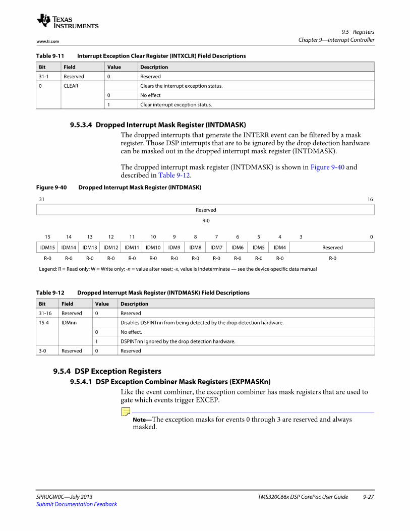
9.5 Registers
SPRUGW0C—July 2013 TMS320C66x DSP CorePac User Guide 9-27Submit Documentation Feedback
Chapter 9—Interrupt Controllerwww.ti.com
9.5.3.4 Dropped Interrupt Mask Register (INTDMASK)The dropped interrupts that generate the INTERR event can be filtered by a mask register. Those DSP interrupts that are to be ignored by the drop detection hardware can be masked out in the dropped interrupt mask register (INTDMASK).
The dropped interrupt mask register (INTDMASK) is shown in Figure 9-40 and described in Table 9-12.
9.5.4 DSP Exception Registers9.5.4.1 DSP Exception Combiner Mask Registers (EXPMASKn)
Like the event combiner, the exception combiner has mask registers that are used to gate which events trigger EXCEP.
Note—The exception masks for events 0 through 3 are reserved and always masked.
Table 9-11 Interrupt Exception Clear Register (INTXCLR) Field Descriptions
Bit Field Value Description
31-1 Reserved 0 Reserved
0 CLEAR Clears the interrupt exception status.
0 No effect
1 Clear interrupt exception status.
Figure 9-40 Dropped Interrupt Mask Register (INTDMASK)
31 16
Reserved
R-0
15 14 13 12 11 10 9 8 7 6 5 4 3 0
IDM15 IDM14 IDM13 IDM12 IDM11 IDM10 IDM9 IDM8 IDM7 IDM6 IDM5 IDM4 Reserved
R-0 R-0 R-0 R-0 R-0 R-0 R-0 R-0 R-0 R-0 R-0 R-0 R-0
Legend: R = Read only; W = Write only; -n = value after reset; -x, value is indeterminate — see the device-specific data manual
Table 9-12 Dropped Interrupt Mask Register (INTDMASK) Field Descriptions
Bit Field Value Description
31-16 Reserved 0 Reserved
15-4 IDMnn Disables DSPINTnn from being detected by the drop detection hardware.
0 No effect.
1 DSPINTnn ignored by the drop detection hardware.
3-0 Reserved 0 Reserved
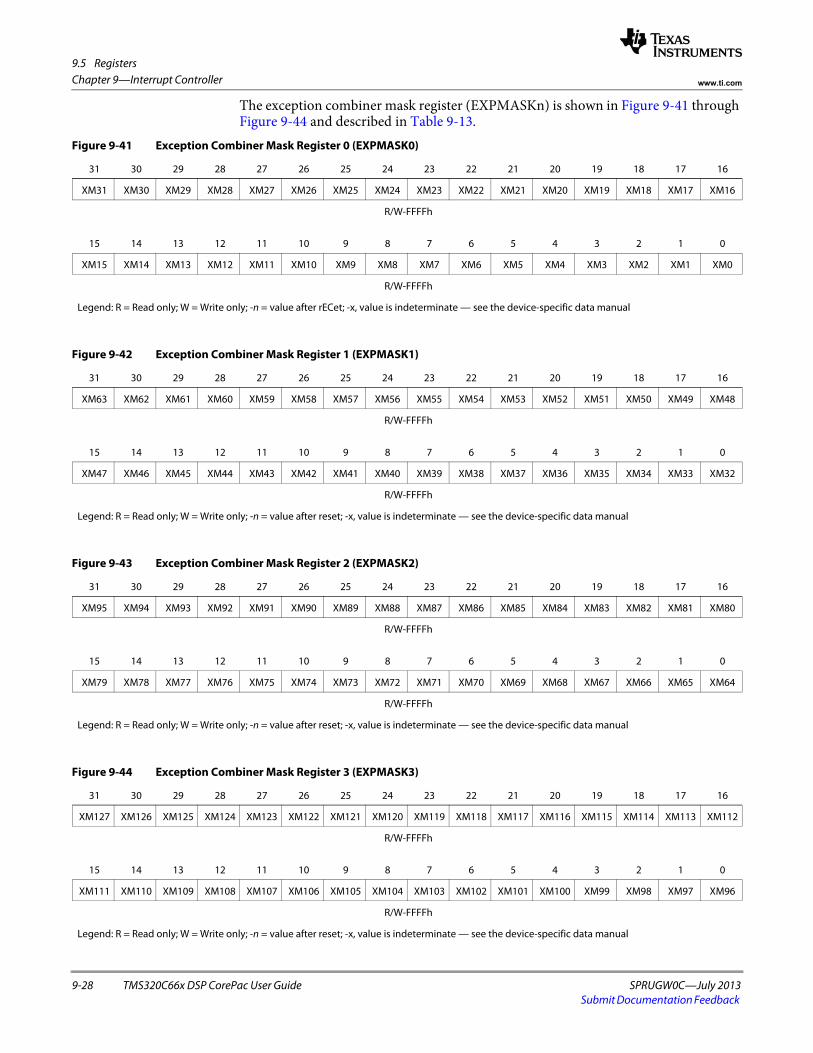
9.5 Registers
9-28 TMS320C66x DSP CorePac User Guide SPRUGW0C—July 2013Submit Documentation Feedback
Chapter 9—Interrupt Controller www.ti.com
The exception combiner mask register (EXPMASKn) is shown in Figure 9-41 through Figure 9-44 and described in Table 9-13.
Figure 9-41 Exception Combiner Mask Register 0 (EXPMASK0)
31 30 29 28 27 26 25 24 23 22 21 20 19 18 17 16
XM31 XM30 XM29 XM28 XM27 XM26 XM25 XM24 XM23 XM22 XM21 XM20 XM19 XM18 XM17 XM16
R/W-FFFFh
15 14 13 12 11 10 9 8 7 6 5 4 3 2 1 0
XM15 XM14 XM13 XM12 XM11 XM10 XM9 XM8 XM7 XM6 XM5 XM4 XM3 XM2 XM1 XM0
R/W-FFFFh
Legend: R = Read only; W = Write only; -n = value after rECet; -x, value is indeterminate — see the device-specific data manual
Figure 9-42 Exception Combiner Mask Register 1 (EXPMASK1)
31 30 29 28 27 26 25 24 23 22 21 20 19 18 17 16
XM63 XM62 XM61 XM60 XM59 XM58 XM57 XM56 XM55 XM54 XM53 XM52 XM51 XM50 XM49 XM48
R/W-FFFFh
15 14 13 12 11 10 9 8 7 6 5 4 3 2 1 0
XM47 XM46 XM45 XM44 XM43 XM42 XM41 XM40 XM39 XM38 XM37 XM36 XM35 XM34 XM33 XM32
R/W-FFFFh
Legend: R = Read only; W = Write only; -n = value after reset; -x, value is indeterminate — see the device-specific data manual
Figure 9-43 Exception Combiner Mask Register 2 (EXPMASK2)
31 30 29 28 27 26 25 24 23 22 21 20 19 18 17 16
XM95 XM94 XM93 XM92 XM91 XM90 XM89 XM88 XM87 XM86 XM85 XM84 XM83 XM82 XM81 XM80
R/W-FFFFh
15 14 13 12 11 10 9 8 7 6 5 4 3 2 1 0
XM79 XM78 XM77 XM76 XM75 XM74 XM73 XM72 XM71 XM70 XM69 XM68 XM67 XM66 XM65 XM64
R/W-FFFFh
Legend: R = Read only; W = Write only; -n = value after reset; -x, value is indeterminate — see the device-specific data manual
Figure 9-44 Exception Combiner Mask Register 3 (EXPMASK3)
31 30 29 28 27 26 25 24 23 22 21 20 19 18 17 16
XM127 XM126 XM125 XM124 XM123 XM122 XM121 XM120 XM119 XM118 XM117 XM116 XM115 XM114 XM113 XM112
R/W-FFFFh
15 14 13 12 11 10 9 8 7 6 5 4 3 2 1 0
XM111 XM110 XM109 XM108 XM107 XM106 XM105 XM104 XM103 XM102 XM101 XM100 XM99 XM98 XM97 XM96
R/W-FFFFh
Legend: R = Read only; W = Write only; -n = value after reset; -x, value is indeterminate — see the device-specific data manual
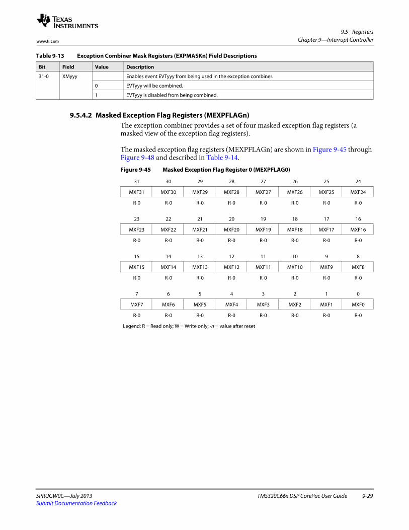
9.5 Registers
SPRUGW0C—July 2013 TMS320C66x DSP CorePac User Guide 9-29Submit Documentation Feedback
Chapter 9—Interrupt Controllerwww.ti.com
9.5.4.2 Masked Exception Flag Registers (MEXPFLAGn)The exception combiner provides a set of four masked exception flag registers (a masked view of the exception flag registers).
The masked exception flag registers (MEXPFLAGn) are shown in Figure 9-45 through Figure 9-48 and described in Table 9-14.
Table 9-13 Exception Combiner Mask Registers (EXPMASKn) Field Descriptions
Bit Field Value Description
31-0 XMyyy Enables event EVTyyy from being used in the exception combiner.
0 EVTyyy will be combined.
1 EVTyyy is disabled from being combined.
Figure 9-45 Masked Exception Flag Register 0 (MEXPFLAG0)
31 30 29 28 27 26 25 24
MXF31 MXF30 MXF29 MXF28 MXF27 MXF26 MXF25 MXF24
R-0 R-0 R-0 R-0 R-0 R-0 R-0 R-0
23 22 21 20 19 18 17 16
MXF23 MXF22 MXF21 MXF20 MXF19 MXF18 MXF17 MXF16
R-0 R-0 R-0 R-0 R-0 R-0 R-0 R-0
15 14 13 12 11 10 9 8
MXF15 MXF14 MXF13 MXF12 MXF11 MXF10 MXF9 MXF8
R-0 R-0 R-0 R-0 R-0 R-0 R-0 R-0
7 6 5 4 3 2 1 0
MXF7 MXF6 MXF5 MXF4 MXF3 MXF2 MXF1 MXF0
R-0 R-0 R-0 R-0 R-0 R-0 R-0 R-0
Legend: R = Read only; W = Write only; -n = value after reset
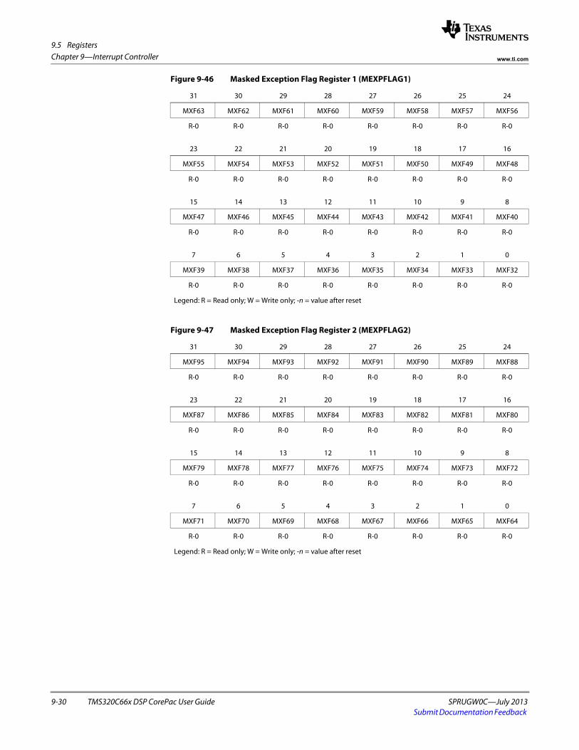
9.5 Registers
9-30 TMS320C66x DSP CorePac User Guide SPRUGW0C—July 2013Submit Documentation Feedback
Chapter 9—Interrupt Controller www.ti.com
Figure 9-46 Masked Exception Flag Register 1 (MEXPFLAG1)
31 30 29 28 27 26 25 24
MXF63 MXF62 MXF61 MXF60 MXF59 MXF58 MXF57 MXF56
R-0 R-0 R-0 R-0 R-0 R-0 R-0 R-0
23 22 21 20 19 18 17 16
MXF55 MXF54 MXF53 MXF52 MXF51 MXF50 MXF49 MXF48
R-0 R-0 R-0 R-0 R-0 R-0 R-0 R-0
15 14 13 12 11 10 9 8
MXF47 MXF46 MXF45 MXF44 MXF43 MXF42 MXF41 MXF40
R-0 R-0 R-0 R-0 R-0 R-0 R-0 R-0
7 6 5 4 3 2 1 0
MXF39 MXF38 MXF37 MXF36 MXF35 MXF34 MXF33 MXF32
R-0 R-0 R-0 R-0 R-0 R-0 R-0 R-0
Legend: R = Read only; W = Write only; -n = value after reset
Figure 9-47 Masked Exception Flag Register 2 (MEXPFLAG2)
31 30 29 28 27 26 25 24
MXF95 MXF94 MXF93 MXF92 MXF91 MXF90 MXF89 MXF88
R-0 R-0 R-0 R-0 R-0 R-0 R-0 R-0
23 22 21 20 19 18 17 16
MXF87 MXF86 MXF85 MXF84 MXF83 MXF82 MXF81 MXF80
R-0 R-0 R-0 R-0 R-0 R-0 R-0 R-0
15 14 13 12 11 10 9 8
MXF79 MXF78 MXF77 MXF76 MXF75 MXF74 MXF73 MXF72
R-0 R-0 R-0 R-0 R-0 R-0 R-0 R-0
7 6 5 4 3 2 1 0
MXF71 MXF70 MXF69 MXF68 MXF67 MXF66 MXF65 MXF64
R-0 R-0 R-0 R-0 R-0 R-0 R-0 R-0
Legend: R = Read only; W = Write only; -n = value after reset

9.5 Registers
SPRUGW0C—July 2013 TMS320C66x DSP CorePac User Guide 9-31Submit Documentation Feedback
Chapter 9—Interrupt Controllerwww.ti.com
9.5.5 Advanced Event Generator Mux Registers (AEGMUXn)The Advanced Event Generator (AEG) allows any event to act as emulation triggers. The events that are sent to the AEG block are configured in the AEG mux registers (AEGMUX0 and AEGMUX1).
The AEGMUX registers are similar to the interrupt selector registers, in that the event to be passed on is simply encoded into a selector bitfield. The encoded value selects between the available system events (EVT[127:4], combined system events (EVT[3:0], the DSP interrupts (DSPINT[15:4], any interrupt acknowledge (IACK), and exception acknowledge (EACK). The combined events (EVT[3:0] are available and are set as the default events.
Note—The AEGMUX0 and AEGMUX1 registers are supported on AET enabled devices only. Refer to your device-specific datasheet to determine if your device supports AET.
Figure 9-48 Masked Exception Flag Register 3 (MEXPFLAG3)
31 30 29 28 27 26 25 24
MXF127 MXF126 MXF125 MXF124 MXF123 MXF122 MXF121 MXF120
R-0 R-0 R-0 R-0 R-0 R-0 R-0 R-0
23 22 21 20 19 18 17 16
MXF119 MXF118 MXF117 MXF116 MXF115 MXF114 MXF113 MXF112
R-0 R-0 R-0 R-0 R-0 R-0 R-0 R-0
15 14 13 12 11 10 9 8
MXF111 MXF110 MXF109 MXF108 MXF107 MXF106 MXF105 MXF104
R-0 R-0 R-0 R-0 R-0 R-0 R-0 R-0
7 6 5 4 3 2 1 0
MXF103 MXF102 MXF101 MXF100 MXF99 MXF98 MXF97 MXF96
R-0 R-0 R-0 R-0 R-0 R-0 R-0 R-0
Legend: R = Read only; W = Write only; -n = value after reset
Table 9-14 Masked Exception Flag Registers (MEXPFLAGn) Field Descriptions
Bit Field Value Description
31-0 MXFyyy 0-FFFF FFFFh Displays content of EFyyy when XMyyy = 0 in the exception mask registers (EXPMASKn).
If (XMyyy = 0) MXFyyy = EFyyy elseMXFyyy = 0

9.5 Registers
9-32 TMS320C66x DSP CorePac User Guide SPRUGW0C—July 2013Submit Documentation Feedback
Chapter 9—Interrupt Controller www.ti.com
The advanced event generator mux registers are shown in Figure 9-49 through Figure 9-50 and described in Table 9-15.
Figure 9-49 Advanced Event Generator Mux Register 0 (AEGMUX0)
31 24 23 16
AEGSEL3 AEGSEL2
R/W-3h R/W-2h
15 8 7 0
AEGSEL1 AEGSEL0
R/W-1h R/W-0h
Legend: R = Read only; W = Write only; -n = value after reset; -x, value is indeterminate — see the device-specific data manual
Figure 9-50 Advanced Event Generator Mux Register 1 (AEGMUX1)
31 24 23 16
AEGSEL7 AEGSEL6
R/W-7h R/W-6h
15 8 7 0
AEGSEL5 AEGSEL4
R/W-5h R/W-4h
Legend: R = Read only; W = Write only; -n = value after reset; -x, value is indeterminate — see the device-specific data manual
Table 9-15 Advanced Event Generator Mux Registers (AEGMUXn) Field Descriptions
Bit Field Value Description
31-0 AEGSELn 0-FFh Advanced event generator (AEG) select.
0-7Fh EVT [127:0]: System events 0 to 127
80-BFh Reserved
C0h EXCEP: DSP Exception
C1h NMI: Non-maskable DSP interrupt
C2-C3h Reserved
C4-CFh DSPINT [15:4]: DSP interrupts
D0-DFh Reserved
E0h IACK: Interrupt acknowledge (for any interrupt)
E1h EACK: Exception acknowledge
E2-E3h Reserved
E4-EFh IACK [15:4]: Interrupt acknowledge for specific DSP interrupts
F0-FFh Reserved
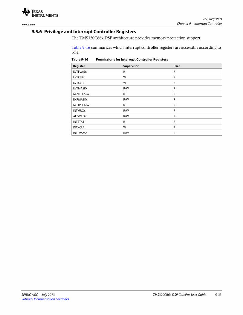
9.5 Registers
SPRUGW0C—July 2013 TMS320C66x DSP CorePac User Guide 9-33Submit Documentation Feedback
Chapter 9—Interrupt Controllerwww.ti.com
9.5.6 Privilege and Interrupt Controller RegistersThe TMS320C66x DSP architecture provides memory protection support.
Table 9-16 summarizes which interrupt controller registers are accessible according to role.Table 9-16 Permissions for Interrupt Controller Registers
Register Supervisor User
EVTFLAGx R R
EVTCLRx W R
EVTSETx W R
EVTMASKx R/W R
MEVTFLAGx R R
EXPMASKx R/W R
MEXPFLAGx R R
INTMUXx R/W R
AEGMUXx R/W R
INTSTAT R R
INTXCLR W R
INTDMASK R/W R

9.5 Registers
9-34 TMS320C66x DSP CorePac User Guide SPRUGW0C—July 2013Submit Documentation Feedback
Chapter 9—Interrupt Controller www.ti.com

SPRUGW0C—July 2013 TMS320C66x DSP CorePac User Guide 10-1Submit Documentation Feedback
Chapter 10
Memory Protection
10.1 "Introduction" on page 10-2 10.2 "Memory Protection Architecture" on page 10-3 10.3 "Memory Protection Registers" on page 10-5 10.4 "Permission Checks on Accesses to Memory Protection Registers" on page 10-12

10.1 Introduction
10-2 TMS320C66x DSP CorePac User Guide SPRUGW0C—July 2013Submit Documentation Feedback
Chapter 10—Memory Protection www.ti.com
10.1 Introduction10.1.1 Purpose of the Memory Protection
Memory protection provides many benefits to a system. Memory protection functionality can:
• Protect operating system data structures from poorly behaving code.• Aid in debugging by providing greater information about illegal memory
accesses.• Allow the operating system to enforce clearly defined boundaries between
supervisor and user mode accesses, leading to greater system robustness.
The C66x CorePac memory protection architecture provides these benefits through a combination of DSP privilege levels and a memory system permission structure.
10.1.2 Privilege Levels The privilege of a thread determines what level of permissions that thread might have.
Code running on the DSP executes in one of two privilege modes: supervisor mode or user mode. Supervisor code is considered more trusted than user code. Examples of supervisor threads include operating system kernels and hardware device drivers. Examples of user threads include vocoders and end applications.
Supervisor mode is generally granted access to peripheral registers and the memory protection configuration. User mode is generally confined to the memory spaces that the OS specifically designates for its use.
DSP accesses as well as internal DMA and other accesses have a privilege level associated with them. The DSP privilege level is determined as described above. The Internal DMA accesses that are initiated by the DSP inherit the DSP's privilege level at the time they are initiated.
10.1.3 Terms and DefinitionsSee Appendix A on page A-1 of this document for a detailed definition of the terms that are used in this chapter.

10.2 Memory Protection Architecture
SPRUGW0C—July 2013 TMS320C66x DSP CorePac User Guide 10-3Submit Documentation Feedback
Chapter 10—Memory Protectionwww.ti.com
10.2 Memory Protection Architecture10.2.1 Memory Protection Pages
The C66x memory protection architecture divides the DSP internal memory (L1P, L1D, L2) into pages. Each page has an associated set of permissions. Section 10.2.2 and its subsections describe the permission sets.
Memories typically have power-of-2 page sizes. The sizes of the L1 and the L2 memory pages are specific to the device. See the device-specific data sheet for more information.
10.2.2 Permission StructureThe memory protection architecture defines a per-page permission structure with two permission fields in a 16-bit permission entry. Figure 10-1 shows the structure of a permission entry.
10.2.2.1 Requestor-ID Based Access Controls Each requestor on the device has an N-bit code associated with it that identifies it for privilege purposes. This ID accompanies all memory accesses and IDMAs made on behalf of that requestor. That is, when a requestor triggers an IDMA transfer directly by writing to IDMA registers, the IDMA engine will provide that ID alongside the transfer. Each DSP and every mastering peripheral (RapidIO, HPI, and EMAC) has an ID. Multiple system masters may share an ID in the same device. Each memory protection entry has an allowed ID field associated with it that indicates which requestors may access the given page. The memory protection hardware maps the IDs of all the possible requestors to bits in the allowed IDs field in the memory protection entries. The allowed IDs field discriminates between various DSPs, non-DSP requestors, and a given DSP's accesses to its own local memories.
• AID0 through AID5 map small-numbered IDs to allowed ID bits. • An additional allowed ID bit, AIDX, captures access made by higher-numbered
PrivIDs.• The LOCAL bit provides special treatment to DSP accesses to its local L1s and L2.
Figure 10-2 illustrates and Table 10-1 describes the allowed IDs bit field.
Figure 10-1 Permission Fields
31 16
Reserved
15 14 13 12 11 10 9 8 7 6 5 4 3 2 1 0
Allowed IDs Reserved Access Types
AID5 AID4 AID3 AID2 AID1 AID0 AIDX LOCAL SR SW SX UR UW UX
Figure 10-2 Allowed IDs Bit Fields
15 14 13 12 11 10 9 8
AID5 AID4 AID3 AID2 AID1 AID0 AIDX LOCAL

10.2 Memory Protection Architecture
10-4 TMS320C66x DSP CorePac User Guide SPRUGW0C—July 2013Submit Documentation Feedback
Chapter 10—Memory Protection www.ti.com
The above ID assignments for bits AID0 through AID5 apply to all IDMA and DSP memory accesses other than to the DSP's local L1 and L2 memories. The LOCAL bit governs DSP accesses to its own local L1 and L2 memories. The AIDX bit maps to IDs that do not have dedicated AID bits associated with them.
10.2.2.2 Request-Type Based PermissionsThe memory protection model defines three fundamental functional access types: read, write, and execute. Read and write refer to data accesses— accesses originating via the load/store units on the DSP or via the IDMA engine. Execute refers to accesses associated with program fetch.
The memory protection model allows controlling read, write, and execute permissions independently for both user and supervisor mode. This results in 6 permission bits, shown in Table 10-2.
For each bit, a 1 permits the access type, and a 0 denies it. Thus UX = 1 means that User Mode may execute from the given page. The memory protection architecture allows you to specify all six of these bits separately. 64 different encodings are permitted altogether, although programs might not use all of them.
10.2.3 Invalid Accesses and Exceptions When it encounters an invalid access, the memory protection hardware has two distinct duties:
• Prevent the access from occurring. • Report the error to the operating environment.
Invalid accesses are those memory accesses which require greater permissions than those specified for the page or register involved. The following sections cover the behavior of the memory protection in the presence of invalid accesses.
Table 10-1 Allowed IDs Bit Field Descriptions
Bit Field Description
15 AID5 Allow accesses from ID = 5
14 AID4 Allow accesses from ID = 4
13 AID3 Allow accesses from ID = 3
12 AID2 Allow accesses from ID = 2
11 AID1 Allow accesses from ID = 1
10 AID0 Allow accesses from ID = 0
9 AIDX Allow accesses from ID > = 6
8 LOCAL Allow access from DSP to its local memories (L1/L2 only)
Table 10-2 Request Type Access Controls
Bit Field Description
5 SR Supervisor may read
4 SW Supervisor may write
3 SX Supervisor may execute
2 UR User may read
1 UW User may write
0 UX User may execute

10.3 Memory Protection Registers
SPRUGW0C—July 2013 TMS320C66x DSP CorePac User Guide 10-5Submit Documentation Feedback
Chapter 10—Memory Protectionwww.ti.com
10.2.3.1 Handling Invalid Accesses When presented with an invalid access, the memory protection prevents the requestor from making the access and will make sure that the memory being protected does not change its state due to the invalid access.
10.2.3.2 Exception Generation Upon detecting an invalid access, the memory protection hardware reports the error to the operating environment.
10.3 Memory Protection RegistersThe memory protection architecture defines several sets of memory-mapped registers (MMRs). Each hardware block that implements memory protection architecture (MPA), implements these MMRs as part of its own register set. As a result, these MMRs reside within its configuration register address space.
The peripherals that implement the MMRs govern accesses to those MMRs. The MMRs fall into three main categories:
• Memory Protection Page Attribute (MPPA) Registers: These registers store the permissions associated with each protected page. These are defined in Section 10.3.1.
• Memory Protection Fault (MPFxR) Registers: Each peripheral that generates memory protection faults provides MPFAR, MPFSR, and MPFCR registers for recording the details of the fault. These are defined in Section 10.3.2 and Section 10.3.2.1.
• Memory Protection Lock (MPLK) Registers: When engaged, the lock disables all updates to the memory protection entries for that peripheral. The MPLK register is defined in Section 10.3.3.
• Because each memory implements its own memory protection registers, see the device-specific data manual for more information about the memory map.
Table 10-3 lists the memory-mapped registers for the memory protection architecture. See the device-specific data manual for the memory address of these registers.
10.3.1 Memory Protection Page Attribute (MPPA) RegistersEach memory that implements a notion of configurable memory protection pages provides a set of memory protection page attribute (MPPA) registers. One MPPA register covers each page that the peripheral implements. These registers typically appear in a contiguous block within the memory's MMR memory map.
Each MPPA register occupies 32 bits in the memory map, but only 16 of these bits are used. Section 10.2.2 describes the layout and definition of the MPPA register fields.
The reset value of the MPPA register is device-dependant.
Table 10-3 Memory Protection Architecture Registers
Acronym Register Description Section
MPPA Memory Protection Page Attribute Section 10.3.1
MPFAR Memory Protection Fault Address Register Section 10.3.2
MPFSR Memory Protection Fault Status Register Section 10.3.2
MPFCR Memory Protection Fault Command Register Section 10.3.2
MPLK Memory Protection Lock Registers Section 10.3.3
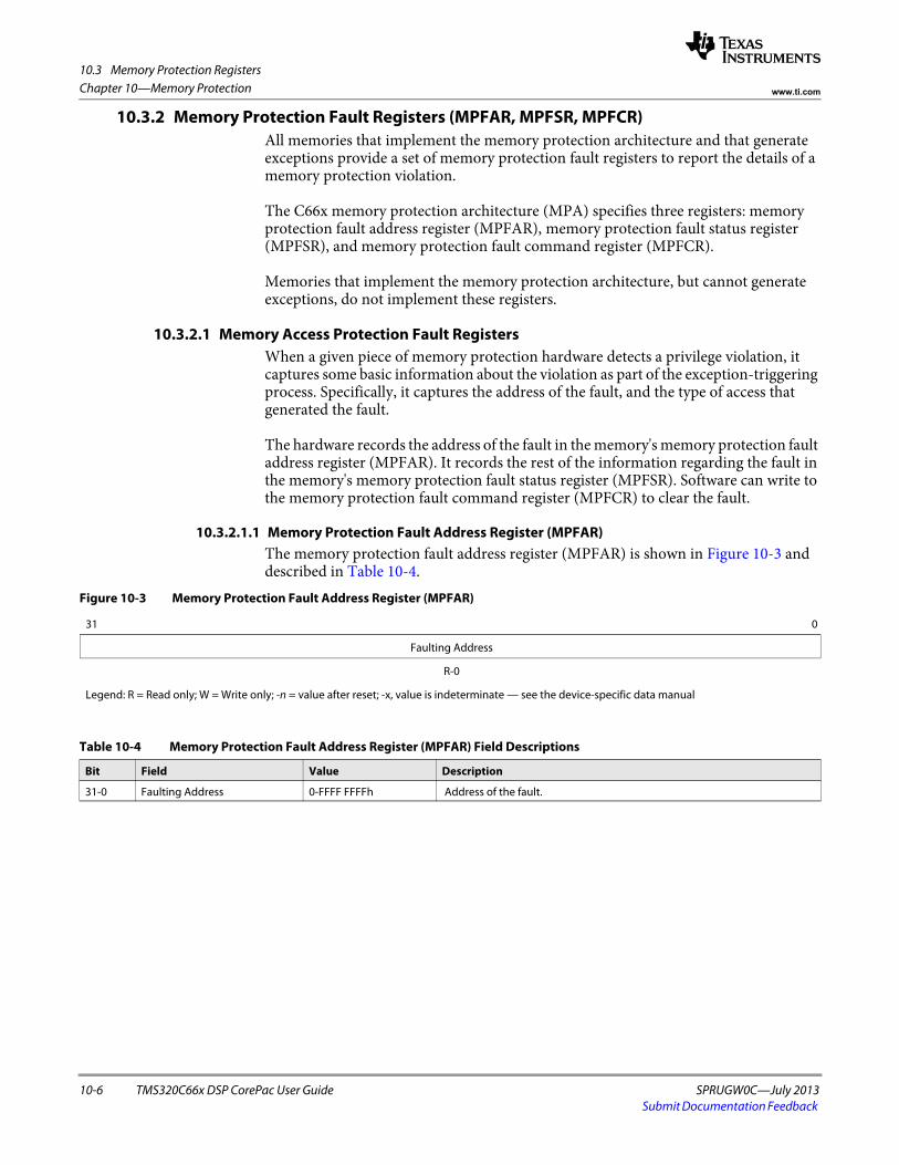
10.3 Memory Protection Registers
10-6 TMS320C66x DSP CorePac User Guide SPRUGW0C—July 2013Submit Documentation Feedback
Chapter 10—Memory Protection www.ti.com
10.3.2 Memory Protection Fault Registers (MPFAR, MPFSR, MPFCR) All memories that implement the memory protection architecture and that generate exceptions provide a set of memory protection fault registers to report the details of a memory protection violation.
The C66x memory protection architecture (MPA) specifies three registers: memory protection fault address register (MPFAR), memory protection fault status register (MPFSR), and memory protection fault command register (MPFCR).
Memories that implement the memory protection architecture, but cannot generate exceptions, do not implement these registers.
10.3.2.1 Memory Access Protection Fault Registers When a given piece of memory protection hardware detects a privilege violation, it captures some basic information about the violation as part of the exception-triggering process. Specifically, it captures the address of the fault, and the type of access that generated the fault.
The hardware records the address of the fault in the memory's memory protection fault address register (MPFAR). It records the rest of the information regarding the fault in the memory's memory protection fault status register (MPFSR). Software can write to the memory protection fault command register (MPFCR) to clear the fault.
10.3.2.1.1 Memory Protection Fault Address Register (MPFAR) The memory protection fault address register (MPFAR) is shown in Figure 10-3 and described in Table 10-4.
Figure 10-3 Memory Protection Fault Address Register (MPFAR)
31 0
Faulting Address
R-0
Legend: R = Read only; W = Write only; -n = value after reset; -x, value is indeterminate — see the device-specific data manual
Table 10-4 Memory Protection Fault Address Register (MPFAR) Field Descriptions
Bit Field Value Description
31-0 Faulting Address 0-FFFF FFFFh Address of the fault.
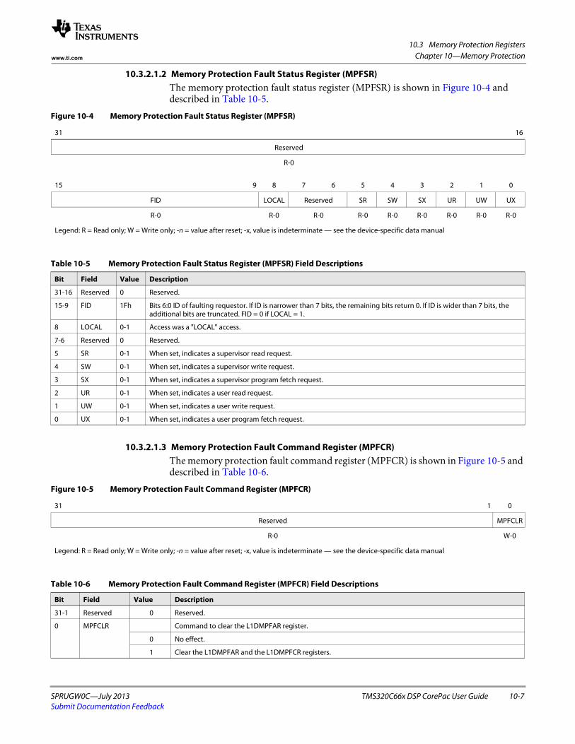
10.3 Memory Protection Registers
SPRUGW0C—July 2013 TMS320C66x DSP CorePac User Guide 10-7Submit Documentation Feedback
Chapter 10—Memory Protectionwww.ti.com
10.3.2.1.2 Memory Protection Fault Status Register (MPFSR)The memory protection fault status register (MPFSR) is shown in Figure 10-4 and described in Table 10-5.
10.3.2.1.3 Memory Protection Fault Command Register (MPFCR)The memory protection fault command register (MPFCR) is shown in Figure 10-5 and described in Table 10-6.
Figure 10-4 Memory Protection Fault Status Register (MPFSR)
31 16
Reserved
R-0
15 9 8 7 6 5 4 3 2 1 0
FID LOCAL Reserved SR SW SX UR UW UX
R-0 R-0 R-0 R-0 R-0 R-0 R-0 R-0 R-0
Legend: R = Read only; W = Write only; -n = value after reset; -x, value is indeterminate — see the device-specific data manual
Table 10-5 Memory Protection Fault Status Register (MPFSR) Field Descriptions
Bit Field Value Description
31-16 Reserved 0 Reserved.
15-9 FID 1Fh Bits 6:0 ID of faulting requestor. If ID is narrower than 7 bits, the remaining bits return 0. If ID is wider than 7 bits, the additional bits are truncated. FID = 0 if LOCAL = 1.
8 LOCAL 0-1 Access was a "LOCAL" access.
7-6 Reserved 0 Reserved.
5 SR 0-1 When set, indicates a supervisor read request.
4 SW 0-1 When set, indicates a supervisor write request.
3 SX 0-1 When set, indicates a supervisor program fetch request.
2 UR 0-1 When set, indicates a user read request.
1 UW 0-1 When set, indicates a user write request.
0 UX 0-1 When set, indicates a user program fetch request.
Figure 10-5 Memory Protection Fault Command Register (MPFCR)
31 1 0
Reserved MPFCLR
R-0 W-0
Legend: R = Read only; W = Write only; -n = value after reset; -x, value is indeterminate — see the device-specific data manual
Table 10-6 Memory Protection Fault Command Register (MPFCR) Field Descriptions
Bit Field Value Description
31-1 Reserved 0 Reserved.
0 MPFCLR Command to clear the L1DMPFAR register.
0 No effect.
1 Clear the L1DMPFAR and the L1DMPFCR registers.
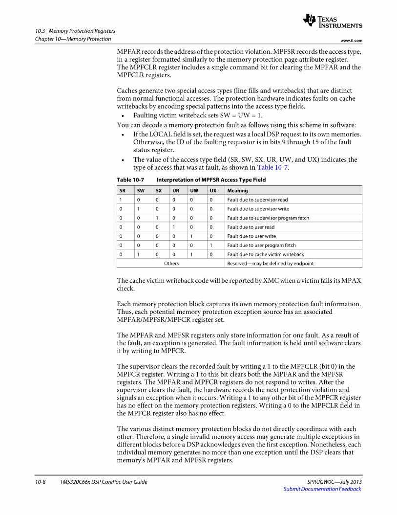
10.3 Memory Protection Registers
10-8 TMS320C66x DSP CorePac User Guide SPRUGW0C—July 2013Submit Documentation Feedback
Chapter 10—Memory Protection www.ti.com
MPFAR records the address of the protection violation. MPFSR records the access type, in a register formatted similarly to the memory protection page attribute register. The MPFCLR register includes a single command bit for clearing the MPFAR and the MPFCLR registers.
Caches generate two special access types (line fills and writebacks) that are distinct from normal functional accesses. The protection hardware indicates faults on cache writebacks by encoding special patterns into the access type fields.
• Faulting victim writeback sets SW = UW = 1. You can decode a memory protection fault as follows using this scheme in software:
• If the LOCAL field is set, the request was a local DSP request to its own memories. Otherwise, the ID of the faulting requestor is in bits 9 through 15 of the fault status register.
• The value of the access type field (SR, SW, SX, UR, UW, and UX) indicates the type of access that was at fault, as shown in Table 10-7.
The cache victim writeback code will be reported by XMC when a victim fails its MPAX check.
Each memory protection block captures its own memory protection fault information. Thus, each potential memory protection exception source has an associated MPFAR/MPFSR/MPFCR register set.
The MPFAR and MPFSR registers only store information for one fault. As a result of the fault, an exception is generated. The fault information is held until software clears it by writing to MPFCR.
The supervisor clears the recorded fault by writing a 1 to the MPFCLR (bit 0) in the MPFCR register. Writing a 1 to this bit clears both the MPFAR and the MPFSR registers. The MPFAR and MPFCR registers do not respond to writes. After the supervisor clears the fault, the hardware records the next protection violation and signals an exception when it occurs. Writing a 1 to any other bit of the MPFCR register has no effect on the memory protection registers. Writing a 0 to the MPFCLR field in the MPFCR register also has no effect.
The various distinct memory protection blocks do not directly coordinate with each other. Therefore, a single invalid memory access may generate multiple exceptions in different blocks before a DSP acknowledges even the first exception. Nonetheless, each individual memory generates no more than one exception until the DSP clears that memory's MPFAR and MPFSR registers.
Table 10-7 Interpretation of MPFSR Access Type Field
SR SW SX UR UW UX Meaning
1 0 0 0 0 0 Fault due to supervisor read
0 1 0 0 0 0 Fault due to supervisor write
0 0 1 0 0 0 Fault due to supervisor program fetch
0 0 0 1 0 0 Fault due to user read
0 0 0 0 1 0 Fault due to user write
0 0 0 0 0 1 Fault due to user program fetch
0 1 0 0 1 0 Fault due to cache victim writeback
Others Reserved—may be defined by endpoint
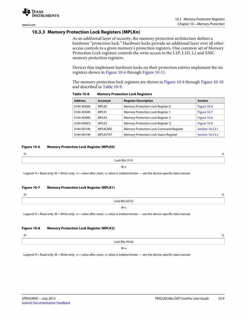
10.3 Memory Protection Registers
SPRUGW0C—July 2013 TMS320C66x DSP CorePac User Guide 10-9Submit Documentation Feedback
Chapter 10—Memory Protectionwww.ti.com
10.3.3 Memory Protection Lock Registers (MPLKn)As an additional layer of security, the memory protection architecture defines a hardware “protection lock.” Hardware locks provide an additional layer over all other access controls to a given memory's protection registers. One common set of Memory Protection Lock registers controls the write access to the L1P, L1D, L2 and XMC memory protection registers.
Devices that implement hardware locks on their protection entries implement the six registers shown in Figure 10-6 through Figure 10-11.
The memory protection lock registers are shown in Figure 10-6 through Figure 10-10 and described in Table 10-9. Table 10-8 Memory Protection Lock Registers
Address Acronym Register Description Section
0184 AD00h MPLK0 Memory Protection Lock Register 0 Figure 10-6
0184 AD04h MPLK1 Memory Protection Lock Register 1 Figure 10-7
0184 AD08h MPLK2 Memory Protection Lock Register 2 Figure 10-8
0184 AD0Ch MPLK3 Memory Protection Lock Register 3 Figure 10-9
0184 AD10h MPLKCMD Memory Protection Lock Command Register Section 10.3.3.1
0184 AD14h MPLKSTAT Memory Protection Lock Status Register Section 10.3.3.2
Figure 10-6 Memory Protection Lock Register (MPLK0)
31 0
Lock Bits 31:0
W-x
Legend: R = Read only; W = Write only; -n = value after reset; -x, value is indeterminate — see the device-specific data manual
Figure 10-7 Memory Protection Lock Register (MPLK1)
31 0
Lock Bits 63:32
W-x
Legend: R = Read only; W = Write only; -n = value after reset; -x, value is indeterminate — see the device-specific data manual
Figure 10-8 Memory Protection Lock Register (MPLK2)
31 0
Lock Bits 95:64
W-x
Legend: R = Read only; W = Write only; -n = value after reset; -x, value is indeterminate — see the device-specific data manual

10.3 Memory Protection Registers
10-10 TMS320C66x DSP CorePac User Guide SPRUGW0C—July 2013Submit Documentation Feedback
Chapter 10—Memory Protection www.ti.com
10.3.3.1 Memory Protection Lock Command Register (MPLKCMD)The memory protection lock command register (MPLKCMD) is shown in Figure 10-10 and described in Table 10-9.
10.3.3.2 Memory Protection Lock Status Register (MPLKSTAT)The memory protection lock status register (MPLKSTAT) is shown in Figure 10-11 and described in Table 10-10.
Figure 10-9 Memory Protection Lock Register (MPLK3)
31 0
Lock Bits 127:96
W-x
Legend: R = Read only; W = Write only; -n = value after reset; -x, value is indeterminate — see the device-specific data manual
Figure 10-10 Memory Protection Lock Command Register (MPLKCMD)
31 3 2 1 0
Reserved KEYR LOCK UNLOCK
R-0 W-0 W-0 W-0
Legend: R = Read only; W = Write only; -n = value after reset; -x, value is indeterminate — see the device-specific data manual
Table 10-9 Memory Protection Lock Command Register (MPLKCMD) Field Descriptions
Bit Field Value Description
31-3 Reserved 0 Reserved.
2 KEYR Reset status.
0 No effect.
1 Reset status.
1 LOCK Interface to complete a lock sequence.
0 No effect.
1 Locks the lock provided that the software executed the sequence correctly.
0 UNLOCK Interface to complete an unlock sequence.
0 No effect.
1 Unlocks the lock provided that software executed the sequence correctly.
Figure 10-11 Memory Protection Lock Status Register (MPLKSTAT)
31 1 0
Reserved LK
R-0 R-0
Legend: R = Read only; W = Write only; -n = value after reset; -x, value is indeterminate — see the device-specific data manual
10.3 Memory Protection Registers
SPRUGW0C—July 2013 TMS320C66x DSP CorePac User Guide 10-11Submit Documentation Feedback
Chapter 10—Memory Protectionwww.ti.com
The lock may exist in one of two states: locked or unlocked. Reset places the lock in the unlocked state via the LK field in the MPLKSTAT register.
Software may engage the lock as long as the lock is currently unlocked. To engage the lock, the application must perform the following steps exactly:
1. Write a 1 to the KEYR field of the MPLKCMD register. This resets the internal status for the MPLK0 through MPLK3 registers.
2. Write the key to MPLK0 through MPLK3. All four registers must be written exactly once. They may be written in any order.
3. Write a 1 to the LOCK field of the MPLKCMD register. This engages the lock.
If programs follow this sequence, the memory protection hardware engages the lock. The hardware performs the following actions when it engages the lock:
• Sets the LK field of the MPLKSTAT register to 1.• Establishes the written key (or some subset) as the “unlock” key • Blocks future writes to all MPPA and MPCFG registers for this memory
The hardware signals an exception if it detects an incorrect lock sequence. The hardware reports the address of the MPLK register written at the point of failure as the exception address in the MPFAR register.
Software executes a sequence similar to the locking sequence to unlock the peripheral's protection registers when they are currently locked:
1. Write a 1 to the KEYR field in the MPLKCMD register. This resets some internal status for the MPLK0 through the MPLK3 registers.
2. Write the unlock key to MPLK0 through the MPLK3 registers. The hardware compares the written value with the stored key value. Software must write to all four registers exactly once. The writes can arrive in any order.
3. Write a 1 to the UNLOCK field in the MPLKCMD register. If the key written in step 2 matches the stored key, the hardware disengages the lock. If the key written in step 2 does not match, the hardware signals an exception. The hardware reports the fault address as the address of the MPLKCMD register.
10.3.4 Keys Shorter than 128 BitsIn some devices, memories may implement keys shorter than 128 bits. In this case, applications that manipulate the lock should write the full 128 bit key when locking and unlocking the lock, even if the hardware does not take the full 128 bits into account.
Table 10-10 Memory Protection Lock Status Register (MPLKSTAT) Field Descriptions
Bit Field Value Description
31-1 Reserved 0 Reserved
0 LK Indicates the lock's current status.
0 Lock is disengaged.
1 Lock is engaged.

10.4 Permission Checks on Accesses to Memory Protection Registers
10-12 TMS320C66x DSP CorePac User Guide SPRUGW0C—July 2013Submit Documentation Feedback
Chapter 10—Memory Protection www.ti.com
10.4 Permission Checks on Accesses to Memory Protection RegistersMemories implementing the memory protection architecture implement permission checks on the memory protection registers. Table 10-11 summarizes these checks:Table 10-11 Allowed Accesses to Memory Protection Registers
Register Set
Supervisor User
Read Write Read Write
MPPAx Always Unlocked Always Never
MPFAR, MPFSR Always Never Always Never
MPFCR Never Always Never Always
MPLK0-MPLK3 Never During lock/unlock sequence Never Never
MPLKSTAT Always Never Always Never
MPLKCMD Never Start/end of lock/unlock Never Never
SPRUGW0C—July 2013 TMS320C66x DSP CorePac User Guide 11-1Submit Documentation Feedback
Chapter 11
Error Detection and Correction (EDC)
11.1 "Overview" on page 11-2 11.2 "L1P Error Detection" on page 11-2 11.3 "L2 Error Detection and Correction" on page 11-6
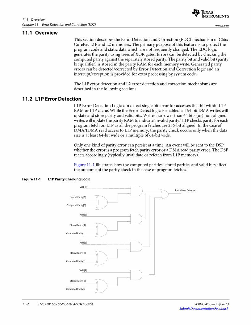
11.1 Overview
11-2 TMS320C66x DSP CorePac User Guide SPRUGW0C—July 2013Submit Documentation Feedback
Chapter 11—Error Detection and Correction (EDC) www.ti.com
11.1 OverviewThis section describes the Error Detection and Correction (EDC) mechanism of C66x CorePac L1P and L2 memories. The primary purpose of this feature is to protect the program code and static data which are not frequently changed. The EDC logic generates the parity using trees of XOR gates. Errors can be detected by checking the computed parity against the separately stored parity. The parity bit and valid bit (parity bit qualifier) is stored in the parity RAM for each memory write. Generated parity errors can be detected/corrected by Error Detection and Correction logic and an interrupt/exception is provided for extra processing by system code.
The L1P error detection and L2 error detection and correction mechanisms are described in the following sections.
11.2 L1P Error DetectionL1P Error Detection Logic can detect single bit error for accesses that hit within L1P RAM or L1P cache. While the Error Detect logic is enabled, all 64-bit DMA writes will update and store parity and valid bits. Writes narrower than 64 bits (or) non-aligned writes will update the parity RAM to indicate ‘invalid parity.’ L1P checks parity for each program fetch on L1P as all the program fetches are 256-bit aligned. In the case of DMA/IDMA read access to L1P memory, the parity check occurs only when the data size is at least 64-bit wide or a multiple of 64-bit wide.
Only one kind of parity error can persist at a time. An event will be sent to the DSP whether the error is a program fetch parity error or a DMA read parity error. The DSP reacts accordingly (typically invalidate or refetch from L1P memory).
Figure 11-1 illustrates how the computed parities, stored parities and valid bits affect the outcome of the parity check in the case of program fetches.
Figure 11-1 L1P Parity Checking Logic
Stored Parity [0]
Computed Parity [0]
Valid [0]
Stored Parity [1]
Computed Parity [1]
Valid [1]
Stored Parity [2]
Computed Parity [2]
Valid [2]
Stored Parity [3]
Computed Parity [3]
Valid [3]
Parity Error Detected
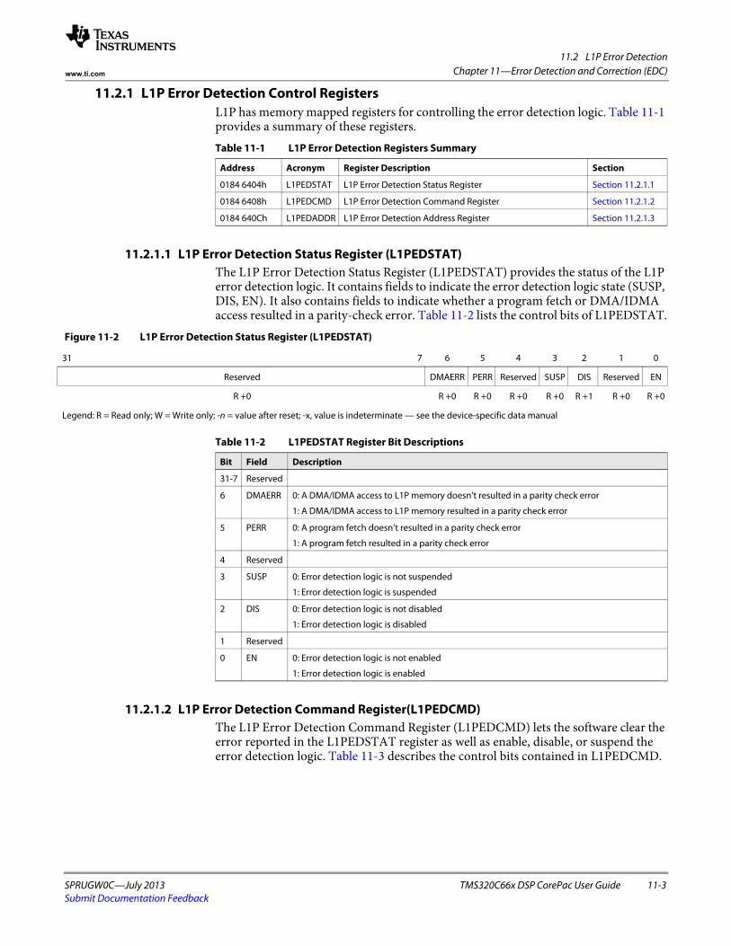
11.2 L1P Error Detection
SPRUGW0C—July 2013 TMS320C66x DSP CorePac User Guide 11-3Submit Documentation Feedback
Chapter 11—Error Detection and Correction (EDC)www.ti.com
11.2.1 L1P Error Detection Control RegistersL1P has memory mapped registers for controlling the error detection logic. Table 11-1 provides a summary of these registers.
11.2.1.1 L1P Error Detection Status Register (L1PEDSTAT)The L1P Error Detection Status Register (L1PEDSTAT) provides the status of the L1P error detection logic. It contains fields to indicate the error detection logic state (SUSP, DIS, EN). It also contains fields to indicate whether a program fetch or DMA/IDMA access resulted in a parity-check error. Table 11-2 lists the control bits of L1PEDSTAT.
11.2.1.2 L1P Error Detection Command Register(L1PEDCMD)The L1P Error Detection Command Register (L1PEDCMD) lets the software clear the error reported in the L1PEDSTAT register as well as enable, disable, or suspend the error detection logic. Table 11-3 describes the control bits contained in L1PEDCMD.
Table 11-1 L1P Error Detection Registers Summary
Address Acronym Register Description Section
0184 6404h L1PEDSTAT L1P Error Detection Status Register Section 11.2.1.1
0184 6408h L1PEDCMD L1P Error Detection Command Register Section 11.2.1.2
0184 640Ch L1PEDADDR L1P Error Detection Address Register Section 11.2.1.3
Figure 11-2 L1P Error Detection Status Register (L1PEDSTAT)
31 7 6 5 4 3 2 1 0
Reserved DMAERR PERR Reserved SUSP DIS Reserved EN
R +0 R +0 R +0 R +0 R +0 R +1 R +0 R +0
Legend: R = Read only; W = Write only; -n = value after reset; -x, value is indeterminate — see the device-specific data manual
Table 11-2 L1PEDSTAT Register Bit Descriptions
Bit Field Description
31-7 Reserved
6 DMAERR 0: A DMA/IDMA access to L1P memory doesn’t resulted in a parity check error
1: A DMA/IDMA access to L1P memory resulted in a parity check error
5 PERR 0: A program fetch doesn’t resulted in a parity check error
1: A program fetch resulted in a parity check error
4 Reserved
3 SUSP 0: Error detection logic is not suspended
1: Error detection logic is suspended
2 DIS 0: Error detection logic is not disabled
1: Error detection logic is disabled
1 Reserved
0 EN 0: Error detection logic is not enabled
1: Error detection logic is enabled

11.2 L1P Error Detection
11-4 TMS320C66x DSP CorePac User Guide SPRUGW0C—July 2013Submit Documentation Feedback
Chapter 11—Error Detection and Correction (EDC) www.ti.com
Writing a ‘0’ to a bit location will not have any effect. Writing a ‘1’ to the location will result in the command associated with that register bit field being executed. Writing ‘1’ to more than one of DIS, EN and SUSP bits in L1PEDCMD will be treated as invalid command and such writes will be dropped by retaining the current EDC mode. L1P memory controller will also trigger an exception when the write is dropped using “L1P_CMPA” event (DSP memory protection fault from L1P).
11.2.1.3 L1P Error Detection Address Register(L1PEDADDR) The L1P Error Detection Address Register (L1PEDADDR) provides the address information for the detected error. Even though the L1P EDC logic operates on 64-bit quanta, the L1PEDADDR records only 256-bit aligned address. Hence it records only the upper 27 bits of the address, the lower 5 bits of the error address is ignored. If there is a parity error during a program fetch, the fetch packet address (which is always aligned to the nearest 256-bit boundary) is recorded. If there is a parity error during a DMA read, the DMA address aligned to the 256-bit address boundary is recorded.
Figure 11-3 L1P Error Detection Command Register (L1PEDCMD)
31 7 6 5 4 3 2 1 0
Reserved DMACLR PCLR Reserved SUSP DIS Reserved EN
R +0 W +0 W +0 R +0 W +0 W +1 R +0 W +0
Legend: R = Read only; W = Write only; -n = value after reset; -x, value is indeterminate — see the device-specific data manual
Table 11-3 L1PEDCMD Register Bit Descriptions
Bit Field Description
31-7 Reserved
6 DMACLR 0: No effect
1: Clears the DMA/IDMA read parity error status
5 PCLR 0: No effect
1: Clears the program fetch parity error status
4 Reserved
3 SUSP 0: No effect
1: Suspends the error detection logic
2 DIS 0: No effect
1: Disables the error detection logic
1 Reserved
0 EN 0: No effect
1: Enables the error detection logic
Figure 11-4 L1P Error Detection Address Register (L1PEDADDR)
31 5 4 1 0
ADDR Reserved RAM
R +0 R +0 R +0
Legend: R = Read only; W = Write only; -n = value after reset; -x, value is indeterminate — see the device-specific data manual

11.2 L1P Error Detection
SPRUGW0C—July 2013 TMS320C66x DSP CorePac User Guide 11-5Submit Documentation Feedback
Chapter 11—Error Detection and Correction (EDC)www.ti.com
11.2.2 L1P Error Detection Logic OperationOn reset, the error detection logic is disabled. While the error detection logic is disabled, writes to L1P will result in the associated valid bits being cleared. Programs enable the Error Detect logic by writing a ‘1’ to the L1P Error Detection Command Register Enable bit (L1PEDCMD.EN = ‘1’). Upon seeing this write, L1P enables the Error Detect logic.
L1P Error Detection Logic does not initialize the parity RAM when transitioning from the disabled to the enabled state. Thus, upon entering the enabled state, there may be invalid parity values in the parity RAM whose corresponding valid bits are also set. To avoid false parity errors for program code executing from L1P RAM, programs should write to all L1P RAM addresses prior to executing code from L1P RAM. Programs executing from L1P cache do not require additional consideration.
While the Error Detect logic is enabled, all 64-bit writes update the stored parity and valid bits. Writes narrower than 64 bits (or) non-aligned writes will update the parity RAM to indicate ‘invalid parity’. All 64-bit reads will be parity checked.
Programs can suspend the Error Detect logic by writing a ‘1’ to L1P Error Detection Command Register Suspend bit (L1PEDCMD.SUSP = ‘1’). While suspended, the L1P neither checks parity nor updates the valid bits. The purpose of this mode is to test this logic in emulation mode.
Programs can disable the Error Detect logic at any time by writing a ‘1’ to L1P Error Detection Command Register Disable bit (L1PEDCMD.DIS = ‘1’). Doing so disables error detection. While in this mode, the L1P clears the ‘valid’ bits on each parity entry whenever it sees a write within L1P.
11.2.3 L1P Error Exception/InterruptL1P provides one error detection exception output “L1P_ED” event. This exception is used to signal that a DMA parity error (DMAERR) was detected during a DMA/IDMA read access to L1P memory. This event is sent to the interrupt controller block in the CorePac, which can then route this to the DSP as interrupt or exception input, as appropriate.
The program fetch parity error (PERR) is signalled as Instruction fetch exception (IERR.IFX) which is routed as a direct exception to the DSP. For further information about IFX error, see the C66x DSP and Instruction Set Reference Guide (SPRUGH7) in ‘‘Related Documentation from Texas Instruments’’ on page ø-xx.
11.2.4 L1P Cache Error Recovery Upon Error DetectionWhen there is a parity error for program fetch from the L1P cache, error detection logic sends a direct exception event to the DSP (IERR.IFX event). In turn, the DSP invalidates program code by flushing the content of the L1P Cache.
Table 11-4 L1PEDADDR Register Bit Descriptions
Bit Field Description
31-5 ADDR Contains the upper 27 bit of error location.
4-1 Reserved
0 RAM 0: error occurred in L1P cache
1: error occurred in L1P RAM
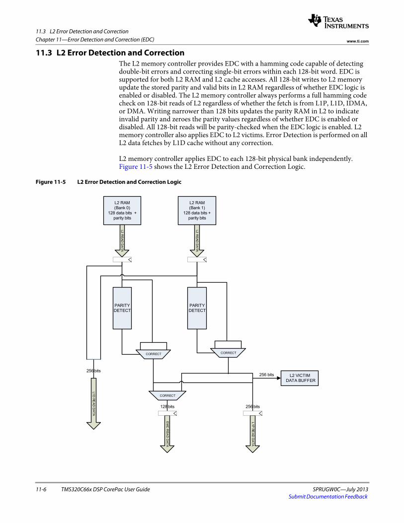
11.3 L2 Error Detection and Correction
11-6 TMS320C66x DSP CorePac User Guide SPRUGW0C—July 2013Submit Documentation Feedback
Chapter 11—Error Detection and Correction (EDC) www.ti.com
11.3 L2 Error Detection and CorrectionThe L2 memory controller provides EDC with a hamming code capable of detecting double-bit errors and correcting single-bit errors within each 128-bit word. EDC is supported for both L2 RAM and L2 cache accesses. All 128-bit writes to L2 memory update the stored parity and valid bits in L2 RAM regardless of whether EDC logic is enabled or disabled. The L2 memory controller always performs a full hamming code check on 128-bit reads of L2 regardless of whether the fetch is from L1P, L1D, IDMA, or DMA. Writing narrower than 128 bits updates the parity RAM in L2 to indicate invalid parity and zeroes the parity values regardless of whether EDC is enabled or disabled. All 128-bit reads will be parity-checked when the EDC logic is enabled. L2 memory controller also applies EDC to L2 victims. Error Detection is performed on all L2 data fetches by L1D cache without any correction.
L2 memory controller applies EDC to each 128-bit physical bank independently. Figure 11-5 shows the L2 Error Detection and Correction Logic.
Figure 11-5 L2 Error Detection and Correction Logic
256 bits
L1D
RE
AD
DA
TA
L2 RAM(Bank 0)
128 data bits + parity bits
L2 RAM(Bank 1)
128 data bits + parity bits
L2 R
EA
D D
ATA
L2 R
EA
D D
ATA
L1P
RE
AD
DA
TA
EM
C R
EA
D D
AT
A
CORRECT
CORRECT
128 bits
PARITYDETECT
PARITYDETECT
CORRECT
L2 VICTIM DATA BUFFER
256 bits
256 bits

11.3 L2 Error Detection and Correction
SPRUGW0C—July 2013 TMS320C66x DSP CorePac User Guide 11-7Submit Documentation Feedback
Chapter 11—Error Detection and Correction (EDC)www.ti.com
11.3.1 L2 Error Detection Control Registers The L2 memory controller has memory-mapped registers for controlling EDC logic. Table 11-5 provides a summary of these registers.
11.3.1.1 L2 Error Detection Status Register(L2EDSTAT)The L2 Error Detection Status Register (L2EDSTAT) provides the status of the error detection logic. It contains fields that indicate an L1P parity error (PERR), an L1D parity error (DERR), DMA parity error (DMAERR) and L2 victim parity error (VERR). It also contains fields to indicate the error detection and parity generation logic state (SUSP, DIS, EN).
L2 memory controller applies EDC to each 128-bit physical bank independently. However the programmer sees error addresses reported at 256-bit granularity. The BITPOS field indicates the location of the bit error within the 256-bit word. The MS-bit of BITPOS reflects which 128-bit half of a 256-bit word contains an error. Table 11-6 lists the control bits of L2EDSTAT.
Table 11-5 L2 Error Detection and Correction Registers Summary
Address Acronym Register Description Section
0184 6004h L2EDSTAT L2 Error Detection Status Register Section 11.3.1.1
0184 6008h L2EDCMD L2 Error Detection Command Register Section 11.3.1.2
0184 600Ch L2EDADDR L2 Error Detection Address Register Section 11.3.1.4
0184 6018h L2EDCPEC L2 Error Detection Correctable Parity Error Counter Register Section 11.3.1.5
0184 601Ch L2EDNPEC L2 Error Detection Non-correctable Parity Error Counter Register
Section 11.3.1.5
0184 6030h L2EDCEN L2 Error Detection and Correction Enable Register Section 11.3.1.3
Figure 11-6 L2 Error Detection Status Register(L2EDSTAT)
31 24 23 16 15 10 9 8 7 6 5 4 3 2 1 0
Reserved BITPOS Reserved NERR VERR DMAERR PERR DERR SUSP DIS Reserved EN
R +0 R +0 R +0 R +0 R +0 R +0 R +0 R +0 R +0 R +1 R +0 R +0
Legend: R = Read only; W = Write only; -n = value after reset; -x, value is indeterminate — see the device-specific data manual
Table 11-6 L2EDSTAT Register Bit Descriptions (Part 1 of 2)
Bit Field Description
31-24 Reserved
23-16 BITPOS BITPOS = 00000000 Single Bit error in position 0
BITPOS = 00000001 Single Bit error in position 1
... ...
BITPOS = 11111110 Single Bit error in position 254
BITPOS = 11111111 Single Bit error in position 255
15-10 Reserved
9-8 NERR NERR = 00 Single Bit error
NERR = 01 Double Bit error
NERR = 10 Reserved
NERR = 11 Error in the parity value., data is correct
7 VERR 0: No parity error occurred on L2 victims
1: Parity error occurred on L2 victims
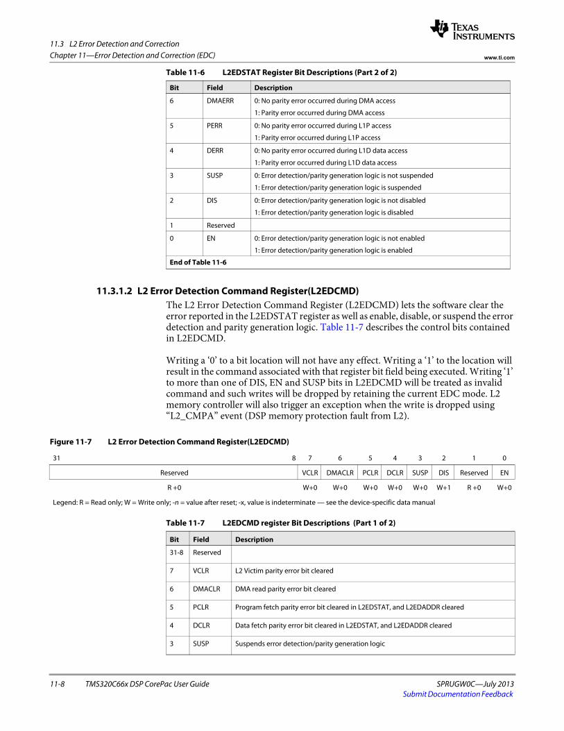
11.3 L2 Error Detection and Correction
11-8 TMS320C66x DSP CorePac User Guide SPRUGW0C—July 2013Submit Documentation Feedback
Chapter 11—Error Detection and Correction (EDC) www.ti.com
11.3.1.2 L2 Error Detection Command Register(L2EDCMD)The L2 Error Detection Command Register (L2EDCMD) lets the software clear the error reported in the L2EDSTAT register as well as enable, disable, or suspend the error detection and parity generation logic. Table 11-7 describes the control bits contained in L2EDCMD.
Writing a ‘0’ to a bit location will not have any effect. Writing a ‘1’ to the location will result in the command associated with that register bit field being executed. Writing ‘1’ to more than one of DIS, EN and SUSP bits in L2EDCMD will be treated as invalid command and such writes will be dropped by retaining the current EDC mode. L2 memory controller will also trigger an exception when the write is dropped using “L2_CMPA” event (DSP memory protection fault from L2).
6 DMAERR 0: No parity error occurred during DMA access
1: Parity error occurred during DMA access
5 PERR 0: No parity error occurred during L1P access
1: Parity error occurred during L1P access
4 DERR 0: No parity error occurred during L1D data access
1: Parity error occurred during L1D data access
3 SUSP 0: Error detection/parity generation logic is not suspended
1: Error detection/parity generation logic is suspended
2 DIS 0: Error detection/parity generation logic is not disabled
1: Error detection/parity generation logic is disabled
1 Reserved
0 EN 0: Error detection/parity generation logic is not enabled
1: Error detection/parity generation logic is enabled
End of Table 11-6
Table 11-6 L2EDSTAT Register Bit Descriptions (Part 2 of 2)
Bit Field Description
Figure 11-7 L2 Error Detection Command Register(L2EDCMD)
31 8 7 6 5 4 3 2 1 0
Reserved VCLR DMACLR PCLR DCLR SUSP DIS Reserved EN
R +0 W+0 W+0 W+0 W+0 W+0 W+1 R +0 W+0
Legend: R = Read only; W = Write only; -n = value after reset; -x, value is indeterminate — see the device-specific data manual
Table 11-7 L2EDCMD register Bit Descriptions (Part 1 of 2)
Bit Field Description
31-8 Reserved
7 VCLR L2 Victim parity error bit cleared
6 DMACLR DMA read parity error bit cleared
5 PCLR Program fetch parity error bit cleared in L2EDSTAT, and L2EDADDR cleared
4 DCLR Data fetch parity error bit cleared in L2EDSTAT, and L2EDADDR cleared
3 SUSP Suspends error detection/parity generation logic
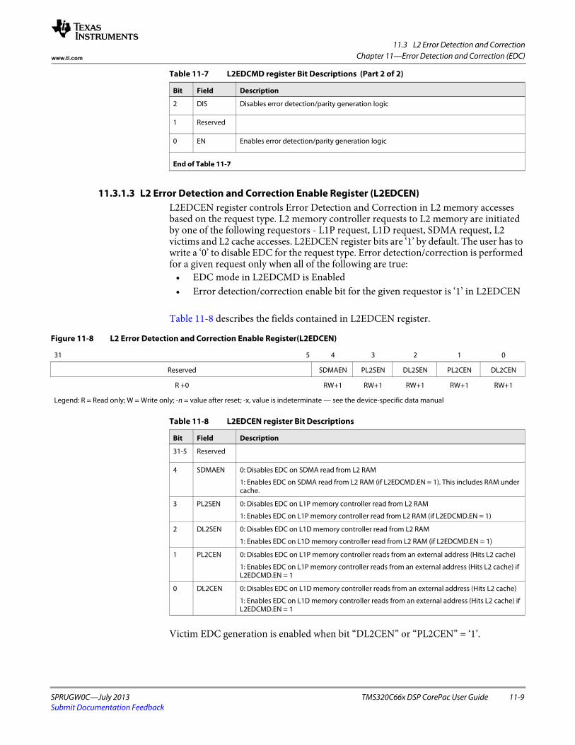
11.3 L2 Error Detection and Correction
SPRUGW0C—July 2013 TMS320C66x DSP CorePac User Guide 11-9Submit Documentation Feedback
Chapter 11—Error Detection and Correction (EDC)www.ti.com
11.3.1.3 L2 Error Detection and Correction Enable Register (L2EDCEN)L2EDCEN register controls Error Detection and Correction in L2 memory accesses based on the request type. L2 memory controller requests to L2 memory are initiated by one of the following requestors - L1P request, L1D request, SDMA request, L2 victims and L2 cache accesses. L2EDCEN register bits are ‘1’ by default. The user has to write a ‘0’ to disable EDC for the request type. Error detection/correction is performed for a given request only when all of the following are true:
• EDC mode in L2EDCMD is Enabled• Error detection/correction enable bit for the given requestor is ‘1’ in L2EDCEN
Table 11-8 describes the fields contained in L2EDCEN register.
Victim EDC generation is enabled when bit “DL2CEN” or “PL2CEN” = ‘1’.
2 DIS Disables error detection/parity generation logic
1 Reserved
0 EN Enables error detection/parity generation logic
End of Table 11-7
Table 11-7 L2EDCMD register Bit Descriptions (Part 2 of 2)
Bit Field Description
Figure 11-8 L2 Error Detection and Correction Enable Register(L2EDCEN)
31 5 4 3 2 1 0
Reserved SDMAEN PL2SEN DL2SEN PL2CEN DL2CEN
R +0 RW+1 RW+1 RW+1 RW+1 RW+1
Legend: R = Read only; W = Write only; -n = value after reset; -x, value is indeterminate — see the device-specific data manual
Table 11-8 L2EDCEN register Bit Descriptions
Bit Field Description
31-5 Reserved
4 SDMAEN 0: Disables EDC on SDMA read from L2 RAM
1: Enables EDC on SDMA read from L2 RAM (if L2EDCMD.EN = 1). This includes RAM under cache.
3 PL2SEN 0: Disables EDC on L1P memory controller read from L2 RAM
1: Enables EDC on L1P memory controller read from L2 RAM (if L2EDCMD.EN = 1)
2 DL2SEN 0: Disables EDC on L1D memory controller read from L2 RAM
1: Enables EDC on L1D memory controller read from L2 RAM (if L2EDCMD.EN = 1)
1 PL2CEN 0: Disables EDC on L1P memory controller reads from an external address (Hits L2 cache)
1: Enables EDC on L1P memory controller reads from an external address (Hits L2 cache) if L2EDCMD.EN = 1
0 DL2CEN 0: Disables EDC on L1D memory controller reads from an external address (Hits L2 cache)
1: Enables EDC on L1D memory controller reads from an external address (Hits L2 cache) if L2EDCMD.EN = 1
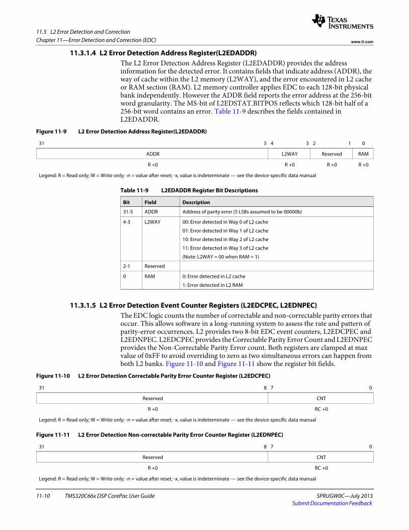
11.3 L2 Error Detection and Correction
11-10 TMS320C66x DSP CorePac User Guide SPRUGW0C—July 2013Submit Documentation Feedback
Chapter 11—Error Detection and Correction (EDC) www.ti.com
11.3.1.4 L2 Error Detection Address Register(L2EDADDR)The L2 Error Detection Address Register (L2EDADDR) provides the address information for the detected error. It contains fields that indicate address (ADDR), the way of cache within the L2 memory (L2WAY), and the error encountered in L2 cache or RAM section (RAM). L2 memory controller applies EDC to each 128-bit physical bank independently. However the ADDR field reports the error address at the 256-bit word granularity. The MS-bit of L2EDSTAT.BITPOS reflects which 128-bit half of a 256-bit word contains an error. Table 11-9 describes the fields contained in L2EDADDR.
11.3.1.5 L2 Error Detection Event Counter Registers (L2EDCPEC, L2EDNPEC)The EDC logic counts the number of correctable and non-correctable parity errors that occur. This allows software in a long-running system to assess the rate and pattern of parity-error occurrences. L2 provides two 8-bit EDC event counters, L2EDCPEC and L2EDNPEC. L2EDCPEC provides the Correctable Parity Error Count and L2EDNPEC provides the Non-Correctable Parity Error count. Both registers are clamped at max value of 0xFF to avoid overriding to zero as two simultaneous errors can happen from both L2 banks. Figure 11-10 and Figure 11-11 show the register bit fields.
Figure 11-9 L2 Error Detection Address Register(L2EDADDR)
31 5 4 3 2 1 0
ADDR L2WAY Reserved RAM
R +0 R +0 R +0 R +0
Legend: R = Read only; W = Write only; -n = value after reset; -x, value is indeterminate — see the device-specific data manual
Table 11-9 L2EDADDR Register Bit Descriptions
Bit Field Description
31-5 ADDR Address of parity error (5 LSBs assumed to be 00000b)
4-3 L2WAY 00: Error detected in Way 0 of L2 cache
01: Error detected in Way 1 of L2 cache
10: Error detected in Way 2 of L2 cache
11: Error detected in Way 3 of L2 cache
(Note: L2WAY = 00 when RAM = 1)
2-1 Reserved
0 RAM 0: Error detected in L2 cache
1: Error detected in L2 RAM
Figure 11-10 L2 Error Detection Correctable Parity Error Counter Register (L2EDCPEC)
31 8 7 0
Reserved CNT
R +0 RC +0
Legend: R = Read only; W = Write only; -n = value after reset; -x, value is indeterminate — see the device-specific data manual
Figure 11-11 L2 Error Detection Non-correctable Parity Error Counter Register (L2EDNPEC)
31 8 7 0
Reserved CNT
R +0 RC +0
Legend: R = Read only; W = Write only; -n = value after reset; -x, value is indeterminate — see the device-specific data manual
11.3 L2 Error Detection and Correction
SPRUGW0C—July 2013 TMS320C66x DSP CorePac User Guide 11-11Submit Documentation Feedback
Chapter 11—Error Detection and Correction (EDC)www.ti.com
11.3.2 L2 EDC Logic OperationThe L2 EDC logic can detect double-bit errors and correct single-bit errors within each 128-bit aligned access. The EDC logic only considers accesses of 128 bits at a time on a 128-bit boundary. Any reads for less than 128 bits or non-aligned to a 128-bit boundary are not checked for parity errors. On each read for 128 bits, the L2 generates the corresponding parity bits. The EDC reads the parity in parallel with the read of L2 memory. This provides the previously-stored parity and valid bits. The EDC compares the computed parity to the stored parity.
The L2 EDC logic updates the stored parity information in response to every 128-bit write on a 128-bit boundary. It calculates the new parity and stores it in the parity RAM along with the valid bit. If the write is less than 128-bits or non-aligned to a 128-bit boundary, L2 updates the parity RAM to indicate invalid parity and zeroes the parity value.
L2 EDC logic generates valid Hamming parity for the following writes:
• L2 line allocations• L1D victims• SDMA and IDMA writes that merged to a full 128 bits• L1D write misses that merged to a full 128 bits
L2 EDC logic invalidates the stored parity on 128-bit words for the following writes:
• L1D write misses that do not write to all 128 bits of a 128-bit word• SDMA and IDMA writes that do not write to all 128 bits of a 128-bit word
On reset, the L2 EDC logic is disabled. Programs enable the EDC logic by writing a '1' to the L2 Error Detection Command Register Enable bit (L2EDCMD.EN = '1'). The L2 EDC logic does not initialize the parity RAM when transitioning from the disabled to the enabled state. Thus, upon entering the enabled state, there may be invalid parity values in the parity RAM whose corresponding valid bits are also set. To avoid false parity errors from L2 RAM, programs should follow the EDC setup sequence mentioned below.
L2 EDC setup sequence:
1. Disable EDC2. Clear any EDC errors3. Memory scrubbing with IDMA (this generates valid parity)4. Enable EDC5. Run application6. Periodic memory scrubbing with IDMA (optional).
See ‘‘Memory Scrubbing Technique’’ on page 11-12 for more information on scrubbing.
Programs can suspend the EDC logic by writing a ‘1’ to the L2 Error Detection Command Register Suspend bit (L2EDCMD.SUSP = ‘1’). While suspended, the L2 neither checks parity nor updates the valid bits. The purpose of this mode is to allow testing of the EDC logic in emulation mode.
11.3 L2 Error Detection and Correction
11-12 TMS320C66x DSP CorePac User Guide SPRUGW0C—July 2013Submit Documentation Feedback
Chapter 11—Error Detection and Correction (EDC) www.ti.com
Program can disable the EDC logic at any time by writing a ‘1’ to the L2 Error Detection Command Register Disable bit (L2EDCMD.DIS = ‘1’). Doing so disables error detection and correction.
11.3.3 Memory Scrubbing TechniqueThe parity and valid bits are set in L2 RAM whenever there is 128-bit aligned write access to L2. Unaligned write access to L2 memory will update the parity RAM to indicate invalid parity.
Programs can ‘scrub’ the memory periodically to ensure that valid parity is set for all addresses of interest. This can be achieved within L2 RAM by using IDMA to read and write a range of L2 RAM addresses. This operation can also be used to correct single-bit parity errors that occur during normal program operation on 128-bit words that already have valid parity.
To scrub a range of memory, the program initiates an IDMA with the source and destination addresses equal to each other; the byte count is set to cover the desired block. The address range must be 128-bit aligned and a multiple of 128-bits for the entire range to be scrubbed. As the IDMA reads the block of memory from L2, the EDC hardware corrects any single-bit errors that might be present on 128-bit words that have valid parity. When IDMA writes the data back to L2, the EDC generates parity for the write and marks it valid.
11.3.4 L2 EDC Exception/InterruptL2 EDC has two signals that route to the DSP through the CorePac interrupt controller. When the EDC logic detects and successfully corrects the error, it sends an error-corrected event “L2_ED1” to the DSP. In response, the DSP can act accordingly by examining the L2ED registers. When EDC logic detects an uncorrectable error, it sends an error-not-corrected event “L2_ED2” to the DSP. Uncorrectable errors include two or more bit errors in a single 128-bit word for all 128-bit wide accesses. This signal is intended to trigger an exception on the DSP. The goal is to prevent invalid data or code from being consumed by an application.
SPRUGW0C—July 2013 TMS320C66x DSP CorePac User Guide 12-1Submit Documentation Feedback
Chapter 12
Power-Down Controller
12.1 "Introduction" on page 12-2 12.2 "Power-Down Features" on page 12-2 12.3 "Power-Down Controller Command Register (PDCCMD) " on page 12-4
12.1 Introduction
12-2 TMS320C66x DSP CorePac User Guide SPRUGW0C—July 2013Submit Documentation Feedback
Chapter 12—Power-Down Controller www.ti.com
12.1 IntroductionThis section provides the purpose and discusses the features of the power-down controller.
12.1.1 C66x CorePac Power-Down Management The C66x CorePac supports the ability to power-down various parts of the C66x CorePac. You can power-down the entire C66x CorePac using the C66x CorePac power-down controller. You can use these features to design systems for lower rate system power requirements.
Note—Peripherals located outside of the C66x CorePac may also provide their own power-down capabilities. These are not covered in this chapter, since they are outside the scope of this document.
12.1.2 Power-Down Capabilities OverviewTable 12-1 lists the power-down features available in the C66x CorePac and a brief description of how and when they are applied:
12.2 Power-Down Features12.2.1 L1P Memory
L1P memory is powered-down dynamically during the execution of instructions from the SPLOOP buffer. This feature is enabled automatically and is transparent to you. Upon completion of the SPLOOP instruction, the DSP resumes fetching from the L1P memory and the RAMs are awakened. In other words, the L1P is powered-down when it is not being accessed. For more information about the SPLOOP instruction, see the C66x DSP and Instruction Set Reference Guide (SPRUGH7) in ‘‘Related Documentation from Texas Instruments’’ on page ø-xx.
Note—L1P is also powered-down when the entire C66x CorePac is powered-down, as described in Section 12.2.5.
12.2.2 L2 MemoryThe C66x CorePac does not support user-controlled dynamic power-down of L2 memory. In KeyStone devices, Retention Until Access (RTA) memories are used as L2 memory. This memory is always in a low leakage mode and wakes up only a block of memory that is accessed and that block is put back into the low leakage mode again. So the L2 memory itself takes care of dynamic page based wakeup automatically.
Note—L2 is also powered-down when the entire C66x CorePac is powered-down (as described in Section 12.2.5).
Table 12-1 C66x CorePac Power-Down Features
Power-Down Feature How/When Applied
L1P memory During SPLOOP instruction execution
L2 memory Retention Until Access (RTA) memories provides dynamic page based wakeup automatically
Cache control hardware When caches are disabled
DSP Upon issuing an IDLE instruction
Entire C66x CorePac Enabled by PDC and IDLE

12.2 Power-Down Features
SPRUGW0C—July 2013 TMS320C66x DSP CorePac User Guide 12-3Submit Documentation Feedback
Chapter 12—Power-Down Controllerwww.ti.com
12.2.3 Cache Power-Down Modes When the L1D, L1P, or L2 caches are not enabled, they are kept in power-down mode.
Note—The three cache controllers are powered-down when the entire C66x CorePac is powered-down (as described in Section 12.2.5).
12.2.4 DSP Power-DownWhile technically outside of the scope of this document, the DSP can be powered-down by issuing an IDLE instruction. The DSP is awakened via interrupt(s). For additional information on the IDLE instruction, see the C66x DSP and Instruction Set Reference Guide (SPRUGH7) in ‘‘Related Documentation from Texas Instruments’’ on page ø-xx.
The IDLE instruction is also used as part of the procedure for powering-down the entire C66x CorePac, as described in Section 12.2.5.
12.2.5 C66x CorePac Powerdown
Note—Powering down the C66x CorePac as described in this section is often called static powerdown. This term is used to describe this power-down mode since this mode is often used for longer periods of time. The term dynamic power-down used in this chapter implies that the power-down mode is used for limited periods of time.
The entire C66x CorePac can be powered-down using the following procedure. Other than the options previously specified, it is not possible to power-down only part of the C66x CorePac. Powering-down the C66x CorePac is completely under software control by programming the C66x CorePac power-down (MEGPD) bit in the power-down controller command register (PDCCMD).
The following software sequence is required to power-down the C66x CorePac:1. Enable power-down by setting the MEGPD field to 1 in the PDCCMD register.2. Enable the DSP interrupt(s) that you want to wake-up the C66x CorePac. Disable
all other interrupts. 3. Execute the IDLE instruction.
The C66x CorePac stays in a power-down state until awakened by the interrupt(s) that are enabled in step 2.
If a DMA access occurs to the L1D, L1P, or L2 memory while the C66x CorePac is powered-down, the PDC wakes all three memory controllers. When the DMA access has been serviced, the PDC will again power-down the memory controllers.
12.2.6 Miscellaneous Power-Down12.2.6.1 Externally-Requested Power-Down
It may be desirable in some systems for the C66x CorePac to respond to an externally-driven power-down request. This can be accomplished, but only under DSP control, using the procedure described in Section 12.2.5.

12.3 Power-Down Controller Command Register (PDCCMD)
12-4 TMS320C66x DSP CorePac User Guide SPRUGW0C—July 2013Submit Documentation Feedback
Chapter 12—Power-Down Controller www.ti.com
External power-down requests are typically accomplished by using external hardware interrupts/exceptions. The interrupt service routine could follow the C66x CorePac power-down procedure to honor the external request.
12.2.6.2 C62x/C64x/C67x DSP Power-Down Modes The power-down modes found in legacy devices (set through the control status register (CSR) in the DSP) are not supported in C64x+/C66x CorePac.
12.3 Power-Down Controller Command Register (PDCCMD) Use the power-down command register (PDCCMD) to program the PDC (located at address 0181 0000h). By setting the MEGPD bit to 1 in the PDCCMD register, the C66x CorePac global static power-down mode is enabled; when the MEGPD register is set to 1, the C66x CorePac global static power-down mode is activated when the DSP enters the idle state. PDCCMD is only writeable when the DSP is in supervisor mode; PDCCMD is readable regardless of supervisor/user status.
The power-down controller command register (PDCCMD) is shown in Figure 12-1 and described in Table 12-2.
Table 12-3 summarizes who may access the power-down controller command register.
Figure 12-1 Power-Down Controller Command Register (PDCCMD) (0181 0000h)
31 17 16
Reserved MEGPD
R-0 R/W-0
15 0
Reserved
RW-xxxxh
Legend: R = Read only; W = Write only; -n = value after reset; -x, value is indeterminate — see the device-specific data manual
Table 12-2 Power-Down Controller Command Register (PDCCMD) Field Descriptions
Bits Field Value Description
31-17 Reserved 0 Reserved.
16 MEGPD Power-down during IDLE
0 Normal operation. Do not power-down the DSP or the C66x CorePac when the DSP is IDLE.
1 Sleep mode. Power-down the DSP and the C66x CorePac when the DSP enters the IDLE state.
15-0 Reserved x Reserved.
Table 12-3 Permissions for PDC Command Register
Register Supervisor User
PDCCMD R/W R

SPRUGW0C—July 2013 TMS320C66x DSP CorePac User Guide 13-1Submit Documentation Feedback
Chapter 13
Miscellaneous
13.1 "Introduction" on page 13-2 13.2 "C66x CorePac Revision ID Register (MM_REVID) " on page 13-2
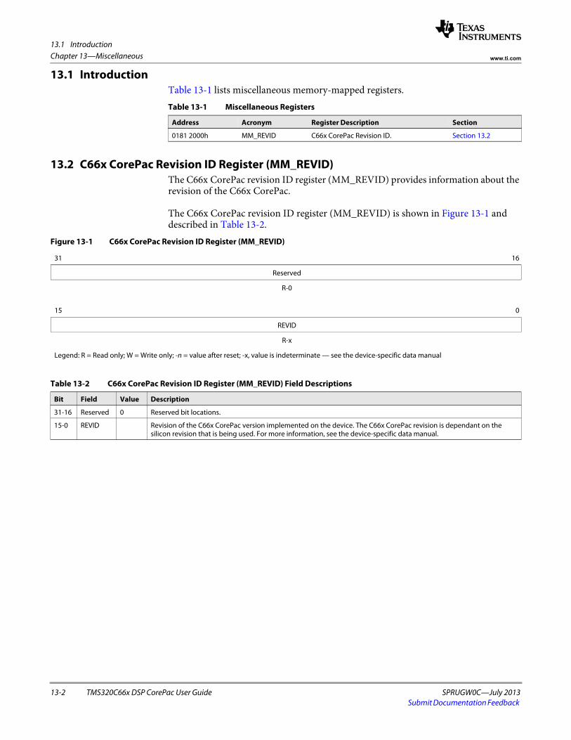
13.1 Introduction
13-2 TMS320C66x DSP CorePac User Guide SPRUGW0C—July 2013Submit Documentation Feedback
Chapter 13—Miscellaneous www.ti.com
13.1 IntroductionTable 13-1 lists miscellaneous memory-mapped registers.
13.2 C66x CorePac Revision ID Register (MM_REVID) The C66x CorePac revision ID register (MM_REVID) provides information about the revision of the C66x CorePac.
The C66x CorePac revision ID register (MM_REVID) is shown in Figure 13-1 and described in Table 13-2.
Table 13-1 Miscellaneous Registers
Address Acronym Register Description Section
0181 2000h MM_REVID C66x CorePac Revision ID. Section 13.2
Figure 13-1 C66x CorePac Revision ID Register (MM_REVID)
31 16
Reserved
R-0
15 0
REVID
R-x
Legend: R = Read only; W = Write only; -n = value after reset; -x, value is indeterminate — see the device-specific data manual
Table 13-2 C66x CorePac Revision ID Register (MM_REVID) Field Descriptions
Bit Field Value Description
31-16 Reserved 0 Reserved bit locations.
15-0 REVID Revision of the C66x CorePac version implemented on the device. The C66x CorePac revision is dependant on the silicon revision that is being used. For more information, see the device-specific data manual.

SPRUGW0C—July 2013 TMS320C66x DSP CorePac User Guide A-1Submit Documentation Feedback
Appendix A
General Terms and Definitions
Table A-1 lists the general terms used throughout this document. Table A-1 List of General Terms and Definitions
Term Definition
C66x Generic name for the new C6000 DSP architecture.
C66x DSP Designates the DSP hardware (functional units and registers).
C66x CorePac Includes the C66x DSP plus all the supporting hardware for memory, bandwidth management, interrupt, memory protection, and power-down support.
CFG External configuration space, includes the memory-mapped registers outside the C66x CorePac.
EDC Error Detection and Correction.
EMC External Memory Controller.
IDMA Internal DMA. It is a DMA engine that is local to the C66x CorePac. It allows transfer of data between memories local to the C66x CorePac (L1P, L1D, L2) and the external configuration space.
L1D Generic name for the level 1 data memory. This term may refer to the memory itself or the memory controller.
L1P Generic name for the level 1 program memory. This term may refer to the memory itself or the memory controller.
L2 Generic name for the level 2 memory. This term may refer to the memory itself or the memory controller.
MPAX Memory Protection and Address Extension
MSMC Multicore Shared Memory Controller
XMC Extended Memory Controller
End of Table A-1

A-2 TMS320C66x DSP CorePac User Guide SPRUGW0C—July 2013Submit Documentation Feedback
Appendix A—General Terms and Definitions www.ti.com

SPRUGW0C—July 2013 TMS320C66x DSP CorePac User Guide B-1Submit Documentation Feedback
Appendix B
Cache Terms and Definitions
Table B-1 lists the cache-related terms used throughout this document that relate to the C66x memory architecture.Table B-1 List of Cache-Related Terms and Definitions (Part 1 of 4)
Term Definition
Allocation The process of finding a location in the cache to store newly cached data. This process can include evicting data that is presently in the cache to make room for the new data.
Associativity The number of line frames in each set. This is specified as the number of ways in the cache.
Capacity miss A cache miss that occurs because the cache does not have sufficient room to hold the entire working set for a program. Compare with compulsory miss and conflict miss.
Clean A cache line that is valid and that has not been written to by upper levels of memory or the DSP. The opposite state for a valid cache line is dirty.
Coherence Informally, a memory system is coherent if any read of a data item returns the most recently written value of that data item. This includes accesses by the DSP and the EDMA.
Compulsory miss Sometimes referred to as a first-reference miss. A compulsory miss is a cache miss that must occur because the data has had no prior opportunity to be allocated in the cache. Typically, compulsory misses for particular pieces of data occur on the first access of that data. However, some cases can be considered compulsory even if they are not the first reference to the data. Such cases include repeated write misses on the same location in a cache that does not write allocate, and cache misses to non-cacheable locations. Compare with capacity miss and conflict miss.
Conflict miss A cache miss that occurs due to the limited associativity of a cache, rather than due to capacity constraints. A fully-associative cache is able to allocate a newly cached line of data anywhere in the cache. Most caches have much more limited associativity (see set-associative cache), and so are restricted in where they may place data. This results in additional cache misses that a more flexible cache would not experience.
Direct-mapped A direct-mapped cache maps each address in the lower-level memory to a single location in the cache. Multiple locations may map to the same location in the cache. This is in contrast to a multi-way set-associative cache, which selects a place for the data from a set of locations in the cache. A direct-mapped cache can be considered a single-way set-associative cache.
Dirty In a writeback cache, writes that reach a given level in the memory hierarchy may update that level, but not the levels below it. Thus, when a cache line is valid and contains updates that have not been sent to the next lower level, that line is said to be dirty. The opposite state for a valid cache line is clean.
DMA Direct Memory Access. Typically, a DMA operation copies a block of memory from one range of addresses to another, or transfers data between a peripheral and memory. On the C66x DSP, DMA transfers are performed by the enhanced DMA (EDMA) engine. These DMA transfers occur in parallel to program execution. From a cache coherence standpoint, EDMA accesses can be considered accesses by a parallel processor.

B-2 TMS320C66x DSP CorePac User Guide SPRUGW0C—July 2013Submit Documentation Feedback
Appendix B—Cache Terms and Definitions www.ti.com
Eviction The process of removing a line from the cache to make room for newly cached data. Eviction can also occur under user control by requesting a writeback-invalidate for an address or range of addresses from the cache. The evicted line is referred to as the victim. When a victim line is dirty (that is, it contains updated data), the data must be written out to the next level memory to maintain coherency.
Execute packet A block of instructions that begin execution in parallel in a single cycle. An execute packet may contain between 1 and 8 instructions.
Fetch packet A block of 8 instructions that are fetched in a single cycle. One fetch packet may contain multiple execute packets, and thus may be consumed over multiple cycles.
First-reference miss A cache miss that occurs on the first reference to a piece of data. First-reference misses are a form of compulsory miss.
Fully-associative A cache that allows any memory address to be stored at any location within the cache. Such caches are cache very flexible, but usually not practical to build in hardware. They contrast sharply with direct-mapped caches and set-associative caches, both of which have much more restrictive allocation policies. Conceptually, fully-associative caches are useful for distinguishing between conflict misses and capacity misses when analyzing the performance of a direct-mapped or set-associative cache. In terms of set-associative caches, a fully-associative cache is equivalent to a set-associative cache that has as many ways as it does line frames, and that has only one set.
Higher-level memory In a hierarchical memory system, higher-level memories are memories that are closer to the DSP. The highest level in the memory hierarchy is usually the Level 1 (L1) caches. The memories at this level exist directly next to the DSP. Higher-level memories typically act as caches for data from lower-level memory.
Hit A cache hit occurs when the data for a requested memory location is present in the cache. The opposite of a hit is a miss. A cache hit minimizes stalling, since the data can be fetched from the cache much faster than from the source memory. The determination of hit versus miss is made on each level of the memory hierarchy separately-a miss in one level may hit in a lower level.
Invalidate The process of marking valid cache lines as invalid in a particular cache. Alone, this action discards the contents of the affected cache lines, and does not write back any updated data. When combined with a writeback, this effectively updates the next lower level of memory that holds the data, while completely removing the cached data from the given level of memory. Invalidates combined with writebacks are referred to as writeback-invalidates, and are commonly used for retaining coherence between caches.
Least-Recently Used For set-associative caches and fully-associative caches, the least-recently used allocation refers to the (LRU) allocation method used to choose among line frames in a set when allocating space in the cache. When all of the line frames in the set that the address maps to contain valid data, the line frame in the set that was read or written the least recently (furthest back in time) is selected to hold the newly cached data. The selected line frame is then evicted to make room for the new data.
Line A cache line is the smallest block of data that the cache operates on. The cache line is typically much larger than the size of data accesses from the DSP or the next higher level of memory. For instance, although the DSP may request single bytes from memory, on a read miss the cache reads an entire line's worth of data to satisfy the request.
Line frame A location in a cache that holds cached data (one line), an associated tag address, and status information for the line. The status information can include whether the line is valid, dirty, and the current state of that line's least-recently used (LRU).
Line size The size of a single cache line, in bytes.
Load through When a DSP request misses both the first-level and second-level caches, the data is fetched from the external memory and stored to both the first-level and second-level cache simultaneously. A cache that stores data and sends that data to the upper-level cache at the same time is a load-through cache. Using a load-through cache reduces the stall time compared to a cache that first stores the data in a lower level and then sends it to the higher-level cache as a second step.
Long-distance Accesses made by the DSP to a non-cacheable memory. Long-distance accesses are used when accessing access external memory that is not marked as cacheable.
Lower-level memory In a hierarchical memory system, lower-level memories are memories that are further from the DSP. In a C66x DSP system, the lowest level in the hierarchy includes the system memory below Level 2 (L2) and any memory-mapped peripherals.
Table B-1 List of Cache-Related Terms and Definitions (Part 2 of 4)
Term Definition
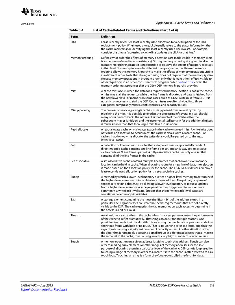
SPRUGW0C—July 2013 TMS320C66x DSP CorePac User Guide B-3Submit Documentation Feedback
Appendix B—Cache Terms and Definitionswww.ti.com
LRU Least Recently Used. See least-recently used allocation for a description of the LRU replacement policy. When used alone, LRU usually refers to the status information that the cache maintains for identifying the least-recently used line in a set. For example, consider the phrase “accessing a cache line updates the LRU for that line.”
Memory ordering Defines what order the effects of memory operations are made visible in memory. (This is sometimes referred to as consistency). Strong memory ordering at a given level in the memory hierarchy indicates it is not possible to observe the effects of memory accesses in that level of memory in an order different than program order. Relaxed memory ordering allows the memory hierarchy to make the effects of memory operations visible in a different order. Note that strong ordering does not require that the memory system execute memory operations in program order, only that it makes their effects visible to other requestors in an order consistent with program order. Section 10.2 covers the memory ordering assurances that the C66x DSP memory hierarchy provides.
Miss A cache miss occurs when the data for a requested memory location is not in the cache. A miss may stall the requestor while the line frame is allocated and data is fetched from the next lower level of memory. In some cases, such as a DSP write miss from L1D, it is not strictly necessary to stall the DSP. Cache misses are often divided into three categories: compulsory misses, conflict misses, and capacity misses.
Miss pipelining The process of servicing a single cache miss is pipelined over several cycles. By pipelining the miss, it is possible to overlap the processing of several misses, should many occur back-to-back. The net result is that much of the overhead for the subsequent misses is hidden, and the incremental stall penalty for the additional misses is much smaller than that for a single miss taken in isolation.
Read allocate A read-allocate cache only allocates space in the cache on a read miss. A write miss does not cause an allocation to occur unless the cache is also a write-allocate cache. For caches that do not write allocate, the write data would be passed on to the next lower-level cache.
Set A collection of line frames in a cache that a single address can potentially reside. A direct-mapped cache contains one line frame per set, and an N-way set-associative cache contains N line frames per set. A fully-associative cache has only one set that contains all of the line frames in the cache.
Set-associative A set-associative cache contains multiple line frames that each lower-level memory location can be held in cache. When allocating room for a new line of data, the selection is made based on the allocation policy for the cache. The C64x+/C66x devices employ a least-recently used allocation policy for its set-associative caches.
Snoop A method by which a lower-level memory queries a higher-level memory to determine if the higher-level memory contains data for a given address. The primary purpose of snoops is to retain coherency, by allowing a lower-level memory to request updates from a higher-level memory. A snoop operation may trigger a writeback, or more commonly, a writeback-invalidate. Snoops that trigger writeback-invalidates are sometimes called snoop-invalidates.
Tag A storage element containing the most-significant bits of the address stored in a particular line. Tag addresses are stored in special tag memories that are not directly visible to the DSP. The cache queries the tag memories on each access to determine if the access is a hit or a miss.
Thrash An algorithm is said to thrash the cache when its access pattern causes the performance of the cache to suffer dramatically. Thrashing can occur for multiple reasons. One possible situation is that the algorithm is accessing too much data or program code in a short time frame with little or no reuse. That is, its working set is too large, and thus the algorithm is causing a significant number of capacity misses. Another situation is that the algorithm is repeatedly accessing a small group of different addresses that all map to the same set in the cache, thus causing an artificially high number of conflict misses.
Touch A memory operation on a given address is said to touch that address. Touch can also refer to reading array elements or other ranges of memory addresses for the sole purpose of allocating them in a particular level of the cache. A DSP-centric loop used for touching a range of memory in order to allocate it into the cache is often referred to as a touch loop. Touching an array is a form of software-controlled pre-fetch for data.
Table B-1 List of Cache-Related Terms and Definitions (Part 3 of 4)
Term Definition
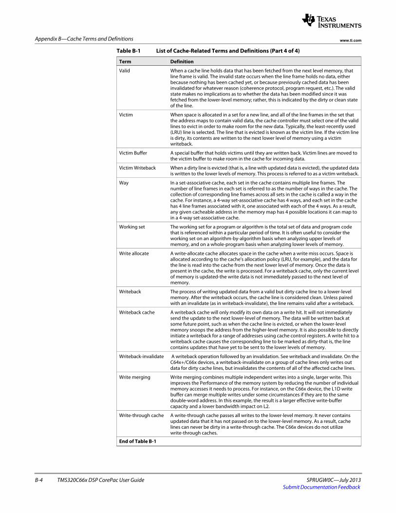
B-4 TMS320C66x DSP CorePac User Guide SPRUGW0C—July 2013Submit Documentation Feedback
Appendix B—Cache Terms and Definitions www.ti.com
Valid When a cache line holds data that has been fetched from the next level memory, that line frame is valid. The invalid state occurs when the line frame holds no data, either because nothing has been cached yet, or because previously cached data has been invalidated for whatever reason (coherence protocol, program request, etc.). The valid state makes no implications as to whether the data has been modified since it was fetched from the lower-level memory; rather, this is indicated by the dirty or clean state of the line.
Victim When space is allocated in a set for a new line, and all of the line frames in the set that the address maps to contain valid data, the cache controller must select one of the valid lines to evict in order to make room for the new data. Typically, the least-recently used (LRU) line is selected. The line that is evicted is known as the victim line. If the victim line is dirty, its contents are written to the next lower level of memory using a victim writeback.
Victim Buffer A special buffer that holds victims until they are written back. Victim lines are moved to the victim buffer to make room in the cache for incoming data.
Victim Writeback When a dirty line is evicted (that is, a line with updated data is evicted), the updated data is written to the lower levels of memory. This process is referred to as a victim writeback.
Way In a set-associative cache, each set in the cache contains multiple line frames. The number of line frames in each set is referred to as the number of ways in the cache. The collection of corresponding line frames across all sets in the cache is called a way in the cache. For instance, a 4-way set-associative cache has 4 ways, and each set in the cache has 4 line frames associated with it, one associated with each of the 4 ways. As a result, any given cacheable address in the memory map has 4 possible locations it can map to in a 4-way set-associative cache.
Working set The working set for a program or algorithm is the total set of data and program code that is referenced within a particular period of time. It is often useful to consider the working set on an algorithm-by-algorithm basis when analyzing upper levels of memory, and on a whole-program basis when analyzing lower levels of memory.
Write allocate A write-allocate cache allocates space in the cache when a write miss occurs. Space is allocated according to the cache's allocation policy (LRU, for example), and the data for the line is read into the cache from the next lower level of memory. Once the data is present in the cache, the write is processed. For a writeback cache, only the current level of memory is updated-the write data is not immediately passed to the next level of memory.
Writeback The process of writing updated data from a valid but dirty cache line to a lower-level memory. After the writeback occurs, the cache line is considered clean. Unless paired with an invalidate (as in writeback-invalidate), the line remains valid after a writeback.
Writeback cache A writeback cache will only modify its own data on a write hit. It will not immediately send the update to the next lower-level of memory. The data will be written back at some future point, such as when the cache line is evicted, or when the lower-level memory snoops the address from the higher-level memory. It is also possible to directly initiate a writeback for a range of addresses using cache control registers. A write hit to a writeback cache causes the corresponding line to be marked as dirty-that is, the line contains updates that have yet to be sent to the lower levels of memory.
Writeback-invalidate A writeback operation followed by an invalidation. See writeback and invalidate. On the C64x+/C66x devices, a writeback-invalidate on a group of cache lines only writes out data for dirty cache lines, but invalidates the contents of all of the affected cache lines.
Write merging Write merging combines multiple independent writes into a single, larger write. This improves the Performance of the memory system by reducing the number of individual memory accesses it needs to process. For instance, on the C66x device, the L1D write buffer can merge multiple writes under some circumstances if they are to the same double-word address. In this example, the result is a larger effective write-buffer capacity and a lower bandwidth impact on L2.
Write-through cache A write-through cache passes all writes to the lower-level memory. It never contains updated data that it has not passed on to the lower-level memory. As a result, cache lines can never be dirty in a write-through cache. The C66x devices do not utilize write-through caches.
End of Table B-1
Table B-1 List of Cache-Related Terms and Definitions (Part 4 of 4)
Term Definition
SPRUGW0C—July 2013 TMS320C66x DSP CorePac User Guide IX-1Submit Documentation Feedback
Index
A AET (Advanced Event Triggering), 9-22, 9-31 architecture, 1-6, 2-2 to 2-4, 2-7, 3-2 to 3-3, 3-18, 4-2 to 4-4, 4-7,
4-12 to 4-13, 4-27 to 4-28, 5-3, 7-13, 8-1, 8-3 to 8-4, 9-3 to 9-4, 9-33, 10-2 to 10-6, 10-9, 10-12, A-1, B-1
B block coherence, 2-7 to 2-8, 3-9, 3-15, 4-8 to 4-9, 4-15 buffer, 2-15, 3-3 to 3-5, 3-10, 3-18, 3-20 to 3-21, 4-13, 4-27, 5-6 to 5-7, 5-12,
5-14, 7-14 to 7-17, 7-19 to 7-20, 12-2, B-4 bus(es), 1-4 to 1-5, 4-36 to 4-37, 6-3 to 6-4, 8-2, 8-4, 8-11, 9-14
C capture mode, 3-20, 9-4 clock, 2-3, 3-2 configuration, 1-4 to 1-5, 2-2 to 2-4, 2-9 to 2-10, 2-14, 3-2 to 3-3,
3-12 to 3-13, 3-21, 4-4 to 4-5, 4-10 to 4-11, 4-14 to 4-15, 4-30, 5-2 to 5-6, 5-10, 6-2 to 6-3, 7-2, 7-7, 7-10, 8-2, 8-4, 8-11, 9-8, 10-2, 10-5, A-1
configuration register, 2-3, 2-9 to 2-10, 3-12 to 3-13, 4-4, 4-14 to 4-15, 5-10, 10-5
CPU, ø-xx
D DDR (Double Data Rate)
DDR3, ø-xx debug, 2-18, 3-24, 4-30 debug mode, 2-18, 3-24, 4-30 detection, 7-14 to 7-15, 9-10, 9-27, 11-1 to 11-12, A-1 DMA (direct memory access), ø-xix, 1-2, 1-4, 2-5, 2-15 to 2-17, 2-21, 3-5,
3-10 to 3-11, 3-18, 3-20, 3-22, 4-6, 4-12 to 4-13, 4-28, 5-14, 6-2, 8-2 to 8-4, 8-7 to 8-10, 9-14, 10-2, 11-2 to 11-8, 12-3, A-1, B-1
DSP, ø-xix, 1-2 to 1-6, 2-2 to 2-6, 2-8, 2-13 to 2-17, 2-21, 3-2 to 3-6, 3-9 to 3-11, 3-18 to 3-25, 4-5 to 4-6, 4-9, 4-11, 4-13, 4-28 to 4-29, 4-32, 4-35, 5-2 to 5-6, 5-8 to 5-9, 5-11 to 5-12, 5-14, 6-2, 7-16, 8-2 to 8-10, 9-2 to 9-3, 9-5 to 9-6, 9-8 to 9-16, 9-22, 9-25 to 9-27, 9-31 to 9-32, 10-2 to 10-4, 10-8, 11-2, 11-4 to 11-5, 11-8, 11-12, 12-2 to 12-4, A-1, B-1 to B-3
E EDMA (Enhanced DMA Controller), 2-2, 5-5, 9-2, B-1 EMAC, 10-3 EMC (External Memory Controller), ø-xix, 1-2, 1-4, 4-29, 5-12 to 5-13,
6-1 to 6-3, 8-4 to 8-9, 8-11, 9-14, A-1
EMIF (External Memory Interface), 1-4 to 1-5, 7-2, 7-7, 7-14, 7-16 EMU (emulation), 7-2 to 7-3, 7-17, 7-20, 9-31, 11-5, 11-11 emulation, 7-2 to 7-3, 7-17, 7-20, 9-31, 11-5, 11-11 error detection, 11-1 to 11-12, A-1 error reporting and messages, 1-5, 4-36 to 4-37, 6-3 to 6-4, 7-19, 9-3,
9-10 to 9-11, 9-14, 10-4 to 10-5, 11-1 to 11-12, A-1
F fault, 1-6, 2-17, 2-20 to 2-21, 3-23 to 3-24, 3-26 to 3-28, 4-30, 4-33 to 4-35,
7-2 to 7-3, 7-10, 7-13, 7-20, 8-10, 9-14, 10-5 to 10-8, 10-11, 11-4, 11-8
G global reset, 4-5
H HPI (Host Processor Interface), 10-3
I inputs, 1-5, 7-17, 9-2, 9-4, 9-9, 9-13 to 9-14 INTC (Interrupt Controller), ø-xix to ø-xx, 1-2, 1-5, 9-2, 9-9 interface, 1-6, 7-2, 7-13, 7-19, 9-15, 10-10 interrupt, ø-xix to ø-xx, 1-2, 1-5, 2-5, 2-15 to 2-17, 3-5, 3-22 to 3-23, 4-7,
4-28 to 4-29, 5-4 to 5-6, 5-11, 5-14, 7-16, 8-5, 9-1 to 9-6, 9-8 to 9-18, 9-21 to 9-22, 9-25 to 9-27, 9-31 to 9-33, 11-2, 11-5, 11-12, 12-3 to 12-4, A-1
L layout, 7-5 to 7-6, 7-20, 10-5
M memory
DMA, ø-xix, 1-2, 1-4, 2-5, 2-15 to 2-17, 2-21, 3-5, 3-10 to 3-11, 3-18, 3-20, 3-22, 4-6, 4-12 to 4-13, 4-28, 5-14, 6-2, 8-2 to 8-4, 8-7 to 8-10, 9-14, 10-2, 11-2 to 11-8, 12-3, A-1, B-1
EMC, ø-xix, 1-2, 1-4, 4-29, 5-12 to 5-13, 6-1 to 6-3, 8-4 to 8-9, 8-11, 9-14, A-1
EMIF, 1-4 to 1-5, 7-2, 7-7, 7-14, 7-16 general, ø-xix to ø-xx, 1-2 to 2-4, 2-7 to 2-9, 2-13, 2-15 to 3-5,
3-8 to 3-12, 3-18 to 4-7, 4-9 to 4-14, 4-19 to 4-36, 5-1 to 5-10, 5-13 to 5-14, 6-1 to 6-3, 7-1 to 7-3, 7-5 to 7-14, 7-16 to 7-17, 8-2, 8-4 to 8-5, 8-7, 8-9 to 8-10, 9-3, 9-14, 9-33, 10-1 to 10-12, 11-2 to 11-12, 12-2 to 12-3, 13-2 to A-1, B-1 to B-4
Index
IX-2 TMS320C66x DSP CorePac User Guide SPRUGW0C—July 2013Submit Documentation Feedback
L1D (Level-One Data Memory), ø-xix, 1-2 to 1-6, 2-2, 2-6 to 2-7, 2-15 to 2-17, 2-19, 3-2 to 3-24, 3-26, 3-28, 4-2, 4-4 to 4-5, 4-7 to 4-15, 4-26 to 4-29, 4-32, 5-2 to 5-4, 5-6, 5-9 to 5-10, 5-12 to 5-13, 6-3, 7-10 to 7-11, 7-14 to 7-15, 7-19, 8-2, 8-4 to 8-6, 8-8 to 8-10, 9-14, 10-3, 10-9, 11-6 to 11-9, 11-11, 12-3, A-1, B-3 to B-4
L1P (Level-One Program Memory), ø-xix, 1-2 to 1-6, 2-2 to 2-17, 2-19 to 2-22, 3-2, 3-7, 3-14, 3-22 to 3-23, 3-26, 4-2, 4-4, 4-7 to 4-9, 4-11 to 4-15, 4-27 to 4-29, 4-32, 5-2 to 5-4, 5-9 to 5-10, 6-3, 7-10 to 7-11, 7-14 to 7-15, 8-2, 8-4 to 8-5, 8-10, 9-14, 10-3, 10-9, 11-2 to 11-9, 12-2 to 12-3, A-1
L2 (Level-Two Unified Memory), ø-xix, 1-2 to 1-6, 2-2, 2-4, 2-9, 2-13 to 2-15, 2-17, 2-19, 3-2 to 3-5, 3-8, 3-10 to 3-12, 3-19 to 3-23, 3-25 to 3-26, 4-2 to 4-20, 4-26 to 4-33, 4-35 to 4-36, 5-2 to 5-4, 5-6, 5-9 to 5-10, 5-12 to 5-13, 6-3, 7-2, 7-10 to 7-11, 7-14 to 7-15, 7-19, 8-2, 8-4 to 8-6, 8-8 to 8-10, 9-14, 10-3 to 10-4, 10-9, 11-2, 11-6 to 11-12, 12-2 to 12-3, A-1, B-2, B-4
map, 1-6, 2-3, 7-6, 7-8, 7-10, 10-5, B-4 MPAX, 1-5, 4-26, 4-36, 7-2 to 7-3, 7-5 to 7-13, 10-8, A-1 MSMC, ø-xx, 1-4 to 1-5, 4-10, 4-26, 7-2, 7-7, 7-11 to 7-12, 7-14, 7-16, A-1 XMC, ø-xix, 1-2, 1-4 to 1-5, 2-17, 3-23, 4-5, 4-10, 4-26 to 4-27, 4-29, 4-36,
7-1 to 7-2, 7-5, 7-7, 7-9 to 7-14, 7-17 to 7-21, 8-9 to 8-10, 10-8 to 10-9, A-1
mode capture, 3-20, 9-4 debug, 2-18, 3-24, 4-30
module, 4-28, 9-9 MPAX (Memory Protection and Address Extension), 1-5, 4-26, 4-36,
7-2 to 7-3, 7-5 to 7-13, 10-8, A-1 MSMC (Multicore Shared Memory Controller), ø-xx, 1-4 to 1-5, 4-10, 4-26,
7-2, 7-7, 7-11 to 7-12, 7-14, 7-16, A-1 mux, 9-4, 9-17, 9-25, 9-31 to 9-32
N NMI (non-maskable interrupt), 9-2, 9-11, 9-15 to 9-16, 9-32
O on-chip, 4-2 output(s), 2-16, 3-23, 4-29, 5-6 to 5-7, 6-3, 7-11, 9-2, 9-7, 9-9 to 9-11,
9-13 to 9-15, 9-22, 11-5 override, 2-14
P performance, 1-5, 2-2, 2-13 to 2-14, 3-2, 3-18, 3-20 to 3-21, 7-2, 7-14, 7-17,
B-2 to B-4
peripherals, 1-4, 1-6, 6-2, 7-12, 9-2, 10-5, 12-2, B-2 polling, 2-7 to 2-8 port, 1-4, 4-3, 4-30, 5-2, 5-12 to 5-13, 6-2, 7-12, 8-5 power
power down, ø-xix, 1-2, 2-15, 12-3 prefetch, 1-4 to 1-5, 4-26 to 4-27, 7-2 to 7-4, 7-14 to 7-20 PrivID (Privilege Identification), 6-2 to 6-3
Q queue, 3-20, 5-4, 5-6
R RAM, 1-4 to 1-5, 2-2 to 2-5, 2-16, 3-2 to 3-3, 3-5, 3-10 to 3-11, 3-18,
4-3 to 4-7, 4-11 to 4-13, 4-20, 5-2, 5-9 to 5-10, 7-2, 7-11 to 7-12, 7-14, 11-2, 11-4 to 11-6, 11-9 to 11-12
RapidIO, 10-3 reset, 1-3, 2-9 to 2-11, 2-18, 2-20 to 2-21, 3-2 to 3-3, 3-12 to 3-16, 3-18,
3-25 to 3-28, 4-5 to 4-6, 4-11, 4-14 to 4-19, 4-26, 4-30 to 4-31, 4-33 to 4-34, 4-36 to 4-37, 5-8 to 5-14, 6-3 to 6-4, 7-7 to 7-8, 7-13, 7-17 to 7-20, 8-5, 8-7 to 8-9, 8-11, 9-2, 9-4 to 9-7, 9-11 to 9-12, 9-15, 9-18 to 9-32, 10-5 to 10-7, 10-9 to 10-11, 11-3 to 11-5, 11-7 to 11-11, 12-4, 13-2
S security
general, 10-9 signal, 1-5, 2-16, 9-2 to 9-3, 9-11 to 9-12, 9-15, 11-5, 11-12 sleep mode, 9-14, 12-4 SRAM (Static RAM), 1-3, 2-2, 2-14, 3-20 to 3-21, 4-11, 8-2 SRIO (Serial RapidIO) subsystem, 1-4, 6-2 status register, 4-10, 5-3, 5-8 to 5-9, 5-12, 7-3, 9-4, 9-10, 9-17, 9-26,
10-5 to 10-11, 11-3, 11-7, 12-4
V version, 8-6, 13-2 video, 5-5
X XMC (eXtended Memory Controller), ø-xix, 1-2, 1-4 to 1-5, 2-17, 3-23, 4-5,
4-10, 4-26 to 4-27, 4-29, 4-36, 7-1 to 7-2, 7-5, 7-7, 7-9 to 7-14, 7-17 to 7-21, 8-9 to 8-10, 10-8 to 10-9, A-1

IMPORTANT NOTICE
Texas Instruments Incorporated and its subsidiaries (TI) reserve the right to make corrections, enhancements, improvements and otherchanges to its semiconductor products and services per JESD46, latest issue, and to discontinue any product or service per JESD48, latestissue. Buyers should obtain the latest relevant information before placing orders and should verify that such information is current andcomplete. All semiconductor products (also referred to herein as “components”) are sold subject to TI’s terms and conditions of salesupplied at the time of order acknowledgment.
TI warrants performance of its components to the specifications applicable at the time of sale, in accordance with the warranty in TI’s termsand conditions of sale of semiconductor products. Testing and other quality control techniques are used to the extent TI deems necessaryto support this warranty. Except where mandated by applicable law, testing of all parameters of each component is not necessarilyperformed.
TI assumes no liability for applications assistance or the design of Buyers’ products. Buyers are responsible for their products andapplications using TI components. To minimize the risks associated with Buyers’ products and applications, Buyers should provideadequate design and operating safeguards.
TI does not warrant or represent that any license, either express or implied, is granted under any patent right, copyright, mask work right, orother intellectual property right relating to any combination, machine, or process in which TI components or services are used. Informationpublished by TI regarding third-party products or services does not constitute a license to use such products or services or a warranty orendorsement thereof. Use of such information may require a license from a third party under the patents or other intellectual property of thethird party, or a license from TI under the patents or other intellectual property of TI.
Reproduction of significant portions of TI information in TI data books or data sheets is permissible only if reproduction is without alterationand is accompanied by all associated warranties, conditions, limitations, and notices. TI is not responsible or liable for such altereddocumentation. Information of third parties may be subject to additional restrictions.
Resale of TI components or services with statements different from or beyond the parameters stated by TI for that component or servicevoids all express and any implied warranties for the associated TI component or service and is an unfair and deceptive business practice.TI is not responsible or liable for any such statements.
Buyer acknowledges and agrees that it is solely responsible for compliance with all legal, regulatory and safety-related requirementsconcerning its products, and any use of TI components in its applications, notwithstanding any applications-related information or supportthat may be provided by TI. Buyer represents and agrees that it has all the necessary expertise to create and implement safeguards whichanticipate dangerous consequences of failures, monitor failures and their consequences, lessen the likelihood of failures that might causeharm and take appropriate remedial actions. Buyer will fully indemnify TI and its representatives against any damages arising out of the useof any TI components in safety-critical applications.
In some cases, TI components may be promoted specifically to facilitate safety-related applications. With such components, TI’s goal is tohelp enable customers to design and create their own end-product solutions that meet applicable functional safety standards andrequirements. Nonetheless, such components are subject to these terms.
No TI components are authorized for use in FDA Class III (or similar life-critical medical equipment) unless authorized officers of the partieshave executed a special agreement specifically governing such use.
Only those TI components which TI has specifically designated as military grade or “enhanced plastic” are designed and intended for use inmilitary/aerospace applications or environments. Buyer acknowledges and agrees that any military or aerospace use of TI componentswhich have not been so designated is solely at the Buyer's risk, and that Buyer is solely responsible for compliance with all legal andregulatory requirements in connection with such use.
TI has specifically designated certain components as meeting ISO/TS16949 requirements, mainly for automotive use. In any case of use ofnon-designated products, TI will not be responsible for any failure to meet ISO/TS16949.
Products Applications
Audio www.ti.com/audio Automotive and Transportation www.ti.com/automotive
Amplifiers amplifier.ti.com Communications and Telecom www.ti.com/communications
Data Converters dataconverter.ti.com Computers and Peripherals www.ti.com/computers
DLP® Products www.dlp.com Consumer Electronics www.ti.com/consumer-apps
DSP dsp.ti.com Energy and Lighting www.ti.com/energy
Clocks and Timers www.ti.com/clocks Industrial www.ti.com/industrial
Interface interface.ti.com Medical www.ti.com/medical
Logic logic.ti.com Security www.ti.com/security
Power Mgmt power.ti.com Space, Avionics and Defense www.ti.com/space-avionics-defense
Microcontrollers microcontroller.ti.com Video and Imaging www.ti.com/video
RFID www.ti-rfid.com
OMAP Applications Processors www.ti.com/omap TI E2E Community e2e.ti.com
Wireless Connectivity www.ti.com/wirelessconnectivity
Mailing Address: Texas Instruments, Post Office Box 655303, Dallas, Texas 75265Copyright © 2013, Texas Instruments Incorporated