c1 10n r4 100k r3 100k - texas instruments op amp u1 is configured as a unity gain voltage follower,...
TRANSCRIPT
An IMPORTANT NOTICE at the end of this TI reference design addresses authorized use, intellectual property matters and other important disclaimers and information.
TINA-TI is a trademark of Texas Instruments WEBENCH is a registered trademark of Texas Instruments
SLAU507-June 2013-Revised June 2013 Low Level (5 µA) V-to-I Converter 1 Copyright © 2013, Texas Instruments Incorporated
Arthur Kay
TI Precision Designs: Verified Design
Low Level (5 µA) V-to-I Converter
TI Precision Designs Circuit Description
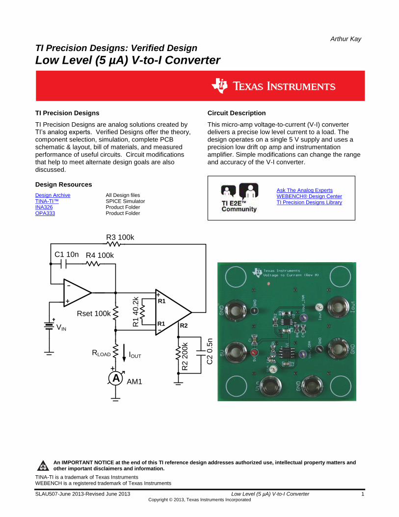
TI Precision Designs are analog solutions created by TI’s analog experts. Verified Designs offer the theory, component selection, simulation, complete PCB schematic & layout, bill of materials, and measured performance of useful circuits. Circuit modifications that help to meet alternate design goals are also discussed.
This micro-amp voltage-to-current (V-I) converter delivers a precise low level current to a load. The design operates on a single 5 V supply and uses a precision low drift op amp and instrumentation amplifier. Simple modifications can change the range and accuracy of the V-I converter.
Design Resources
Design Archive All Design files TINA-TI™ SPICE Simulator INA326 Product Folder OPA333 Product Folder
Ask The Analog Experts WEBENCH® Design Center TI Precision Designs Library
R1
40
.2k R1
R1 R2
C2
0.5
n
R2
20
0k
-
+
A+
AM1
VIN
R3 100k
C1 10n
RLOAD
Rset 100k
-
+
IOUT
R4 100k

www.ti.com
2 Low Level (5 µA) V-to-I Converter SLAU507-June 2013-Revised June 2013 Copyright © 2013, Texas Instruments Incorporated
1 Design Summary
The design requirements are as follows:
Supply Voltage: 5 V dc
Input: 0 V – 5 V dc
Output: 0 µA – 5 µA dc
The design goals and performance are summarized in Table 1. Figure 1 depicts the measured transfer function of the design.
Table 1. Comparison of Design Goals, Simulation, and Measured Performance
Goal Simulated Measured
Uncalibrated Accuracy (%FSR) 0.2% 0.3% 0.18%
Calibrated Accuracy (%FSR) 0.01% na 0.001%
Load Compliance 0<R<500k
Max Linear Output (µA) 4.0 µA 4.9 µA 4.9 µA
Load Compliance 0<R<500k
Min Linear Output (µA) 1.0 µA 0 µA 0.6 µA
Figure 1: Measured Transfer Function
0.0
0.5
1.0
1.5
2.0
2.5
3.0
3.5
4.0
4.5
5.0
0 1 2 3 4 5
Iou
t (µ
A)
Vin (V)
Iout (µA) vs Vin (V)
www.ti.com
SLAU507-June 2013-Revised June 2013 Low Level (5 µA) V-to-I Converter 3 Copyright © 2013, Texas Instruments Incorporated
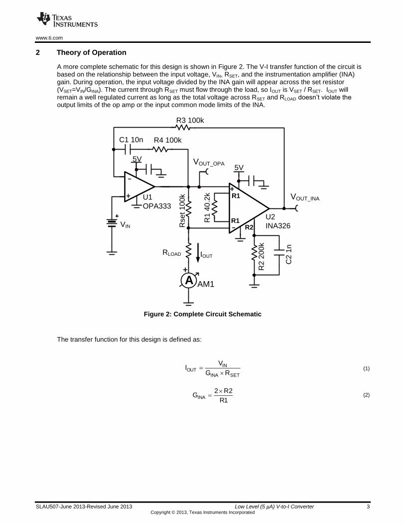
2 Theory of Operation
A more complete schematic for this design is shown in Figure 2. The V-I transfer function of the circuit is based on the relationship between the input voltage, VIN, RSET, and the instrumentation amplifier (INA) gain. During operation, the input voltage divided by the INA gain will appear across the set resistor (VSET=VIN/GINA). The current through RSET must flow through the load, so IOUT is VSET / RSET. IOUT will remain a well regulated current as long as the total voltage across RSET and RLOAD doesn’t violate the output limits of the op amp or the input common mode limits of the INA.
Figure 2: Complete Circuit Schematic
The transfer function for this design is defined as:
SETINA
INOUT
RG
VI
(1)
1R
2R2GINA
(2)
R1
40
.2k R1
R1R2
C2
1n
R2
20
0k
-
+
A+
AM1
VOUT_INA
VIN
R3 100k
C1 10n
RLOAD
Rse
t 1
00k
-
+
IOUT
R4 100k
5V5V
U2
INA326
U1
OPA333
VOUT_OPA
www.ti.com
4 Low Level (5 µA) V-to-I Converter SLAU507-June 2013-Revised June 2013 Copyright © 2013, Texas Instruments Incorporated
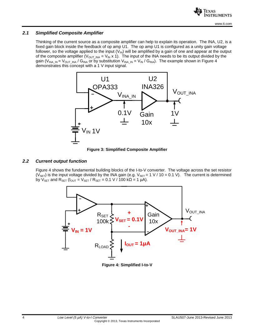
2.1 Simplified Composite Amplifier
Thinking of the current source as a composite amplifier can help to explain its operation. The INA, U2, is a fixed gain block inside the feedback of op amp U1. The op amp U1 is configured as a unity gain voltage follower, so the voltage applied to the input (VIN) will be amplified by a gain of one and appear at the output of the composite amplifier (VOUT_INA = VIN x 1). The input of the INA needs to be its output divided by the gain (VINA_IN = VOUT_INA / GINA or by substitution VINA_IN = VIN / GINA). The example shown in Figure 4 demonstrates this concept with a 1 V input signal.
Figure 3: Simplified Composite Amplifier
2.2 Current output function
Figure 4 shows the fundamental building blocks of the I-to-V converter. The voltage across the set resistor (VSET) is the input voltage divided by the INA gain (e.g. VSET = 1 V / 10 = 0.1 V). The current is determined by VSET and RSET (IOUT = VSET / RSET = 0.1 V / 100 kΩ = 1 µA).
Figure 4: Simplified I-to-V
-
+
VOUT_INA
VIN
Gain
10x
1V
1V0.1V
U2
INA326U1
OPA333VINA_IN
-
+ VOUT_INA
VIN = 1V
RLOAD
RSET
100k
-
+
IOUT = 1μA
Gain
10x
+
VSET = 0.1V
-VOUT_INA= 1V

www.ti.com
SLAU507-June 2013-Revised June 2013 Low Level (5 µA) V-to-I Converter 5 Copyright © 2013, Texas Instruments Incorporated
2.3 Setting the INA Gain
External components (R1, R2, and C2) are used to set the INA gain. The INA gain will determine the maximum voltage across the current setting resistor (RSET). For example, if the gain is 10 V/V, the maximum voltage across RSET is 0.5 V (VSET_MAX = VS / GINA = 5 V / 10 = 0.5 V). Minimizing the voltage across RSET allows for a wider voltage range across the load. In this example, the load voltage can be as high as 4.5 V (Max Load voltage = VS – VSET = 5 V – 0.5 V = 4.5 V). Using a larger gain could further minimize the drop across RSET but introduces other issues. Section 6.5 covers the compliance issues in detail. Section 7.2 also covers trade-offs in selecting different INA gain settings. In this example, the gain is set to 10 V/V. Table 2 shows an excerpt from the INA326 data sheet that was used to select the gain set components (GINA = 10 V/V, R1 = 40.2 kΩ, R2 = 200 kΩ, C2 = 0.5 nF). Note that 40.2 kΩ is the closest standard value to 40 kΩ, so the gain is actually set to 9.95 V/V. This is not really an issue as this circuit is calibrated for highest accuracy.
Table 2: Gain for INA326 in Single Supply Configuration
Desired Gain (V/V)
R1 (Ω) R2 || C2
(Ω || nF)
1 400k 200k || 0.5
10 40k 200k || 0.5
20 20k 200k || 0.5
2.4 Setting the output current range
The output current range is determined by the maximum set voltage (VSET_MAX) and the set resistance RSET. As Section 2.3 indicated, VSET_MAX depends on the supply voltage and the gain. RSET is selected to set the output current range (RSET = VSET_MAX / IOUT_RANGE = 0.5 V / 5 μA = 100 kΩ).
k100A1
V5.0
I
VR
RANGE_OUT
MAX_SETSET (3)
2.5 Compensation Components
External components (C1, R3, and R4) are required to make the V-to-I circuit stable. The value of these components will change for different op amps and instrumentation amplifiers. These components form an ac feedback path for the op amp which prevents peaking in the closed loop response. Because of both the stability compensation components and inherent bandwidth limitations of the INA326 and OPA333 the closed loop frequency response of the system is very low. The procedure for selecting the stability network is beyond the scope of this design note; see reference [1] for a detailed explanation of stability.

www.ti.com
6 Low Level (5 µA) V-to-I Converter SLAU507-June 2013-Revised June 2013 Copyright © 2013, Texas Instruments Incorporated
3 Component Selection
3.1 Op Amp Selection
This design is a high dc precision low level (micro-amp) current source. The key op amp (U1) characteristics needed to get a stable dc output current are input offset voltage (Vos) and offset drift (ΔVos/ΔT). Since the desired input range is 0 V to 5 V a rail-to-rail input amplifier is needed. Also, to avoid error across the common mode range, good CMRR (110db or better) is desirable.
3.2 INA Selection
Low offset, low offset drift, and low bias current are key characteristics of the instrumentation amplifier selection. Low gain error and low gain error drift are secondary characteristics to consider. Since this circuit is calibrated at 25 °C, the drift characteristics are more important than the absolute accuracy. Another important characteristic of the INA is its common mode input range and output swing range. The INA326 amplifier has common mode range beyond the power supply rails (i.e. -0.02 V < Vcm < 5.1 V). Furthermore, the common mode range is not dependent on gain or the reference voltage as is common for many instrumentation amplifiers. The output can swing very close to the power supply rails (5 mV) with a 25 µA load). This excellent common mode and output swing allows for good load compliance (e.g. load voltages can range from nearly 0 V to 5 V).
3.3 Passive Component Selection
The critical passive components for this design are the three resistors that are part of the transfer function, R1, R2, and RSET. To minimize gain error, 0.1%, 20 ppm/°C resistors were used. The low temperature drift (20 ppm/°C) of the resistors is important to get stable results even when the circuit is operated at room temperature. Remember, room temperature can change +/-2 °C over the course of a few minutes even in a well-controlled environment. To get optimal performance the circuit should be calibrated.
Other passive components in this design may be selected for 1% or greater as they will not directly affect the transfer function of this design.

www.ti.com
SLAU507-June 2013-Revised June 2013 Low Level (5 µA) V-to-I Converter 7 Copyright © 2013, Texas Instruments Incorporated
4 Simulation
The TINA-TI™ schematic shown in Figure 5 includes the circuit values obtained in the design process.
+5V
+5V
+5V
V2 5
Rset 100kR
1 1
00
C1 10n
R3 100k
Vout_inaV+
VM1
A+
Iout
Vout_opa
R2 2
00k
C2 5
00p
+
+
-
R1
R1
-
R2
U2 INA326_AK
R1 4
0k
R4 100k
+
-
+U1 OPA333
+
Vin 100m
Figure 5: TINA-TI™ Spice Schematic

www.ti.com
8 Low Level (5 µA) V-to-I Converter SLAU507-June 2013-Revised June 2013 Copyright © 2013, Texas Instruments Incorporated
4.1 DC Transfer Function
The dc transfer function simulation results of the circuit are shown in Figure 6. The results can be used to reference the voltage or current at a given node as a function of the input voltage.
Figure 6: Simulation DC Transfer Results (RL = 500 kΩ)
Figure 7 shows detail on other nodes in the design. For example, the instrumentation amplifier output and op amp output can be observed in Figure 7.
Figure 7: Simulation DC Transfer Results (RL=500 kΩ)
T
Input voltage (V)
0.00 1.00 2.00 3.00 4.00 5.00
Iout
0.00
2.50u
5.00u
T
Vout_opa
for RL = 500k
Input voltage (V)
0.00 1.00 2.00 3.00 4.00 5.00
Iout
0.00
2.50u
5.00u
VM1
0.00
250.01m
500.00m
Vout_ina
0.00
2.50
5.00
Vout_opa
0.00
2.50
5.00
Vout_opa
for RL = 500k

www.ti.com
SLAU507-June 2013-Revised June 2013 Low Level (5 µA) V-to-I Converter 9 Copyright © 2013, Texas Instruments Incorporated
4.2 Step Response
The step response of the design can be seen in Figure 8. The results show that the output of the op amp, INA, and current output settle to the proper values with little overshoot and ringing. This indicates that the design is stable.
Figure 8: Step-Response Simulation
T
Iout
2.01uA
Iout
1.99uA
Time (s)
100.00m 150.00m 200.00m 250.00m 300.00m
Iout
1.99u
2.01u
Vdif
198.59m
201.45m
Vin
1.99
2.01
Vout_ina
1.99
2.01
Vout_opa
1.19
1.21
Iout
1.99uAIout
2.01uA
www.ti.com
10 Low Level (5 µA) V-to-I Converter SLAU507-June 2013-Revised June 2013 Copyright © 2013, Texas Instruments Incorporated
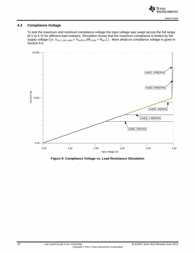
4.3 Compliance Voltage
To test the maximum and minimum compliance voltage the input voltage was swept across the full range (0 V to 5 V) for different load resistors. Simulation shows that the maximum compliance is limited by the supply voltage (i.e. VOUT_OPA_MAX = VSUPPLY/(RLOAD + RSET) ). More detail on compliance voltage is given in Section 6.5.
Figure 9: Compliance Voltage vs. Load Resistance Simulation
T
Iout[1]: 100k[Ohm]
Iout[2]: 500k[Ohm]
Iout[3]: 1M[Ohm]
Iout[4]: 1.5M[Ohm]
Iout[5]: 2M[Ohm]
Input voltage (V)
0.00 1.00 2.00 3.00 4.00 5.00
Curr
ent
(A)
0.00
5.00u
10.00u
Iout[1]: 100k[Ohm]
Iout[2]: 500k[Ohm]
Iout[3]: 1M[Ohm]
Iout[4]: 1.5M[Ohm]
Iout[5]: 2M[Ohm]
www.ti.com
SLAU507-June 2013-Revised June 2013 Low Level (5 µA) V-to-I Converter 11 Copyright © 2013, Texas Instruments Incorporated
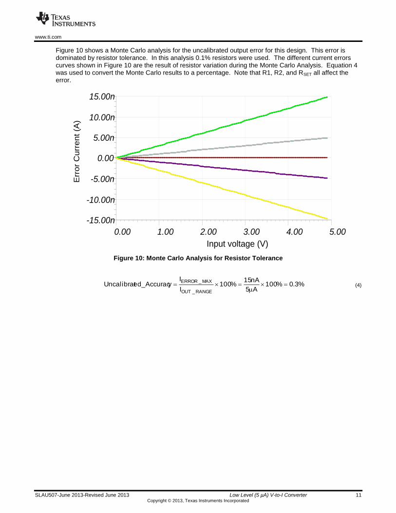
Figure 10 shows a Monte Carlo analysis for the uncalibrated output error for this design. This error is dominated by resistor tolerance. In this analysis 0.1% resistors were used. The different current errors curves shown in Figure 10 are the result of resistor variation during the Monte Carlo Analysis. Equation 4 was used to convert the Monte Carlo results to a percentage. Note that R1, R2, and RSET all affect the error.
Figure 10: Monte Carlo Analysis for Resistor Tolerance
%3.0%100A5
nA15%100
I
Iyed_AccuracUncalibrat
RANGE_OUT
MAX_ERROR
(4)
T
Input voltage (V)
0.00 1.00 2.00 3.00 4.00 5.00
Err
or
Cu
rre
nt (A
)
-15.00n
-10.00n
-5.00n
0.00
5.00n
10.00n
15.00n
www.ti.com
12 Low Level (5 µA) V-to-I Converter SLAU507-June 2013-Revised June 2013 Copyright © 2013, Texas Instruments Incorporated
5 PCB Design
The PCB schematic and bill of materials can be found in Appendix A.
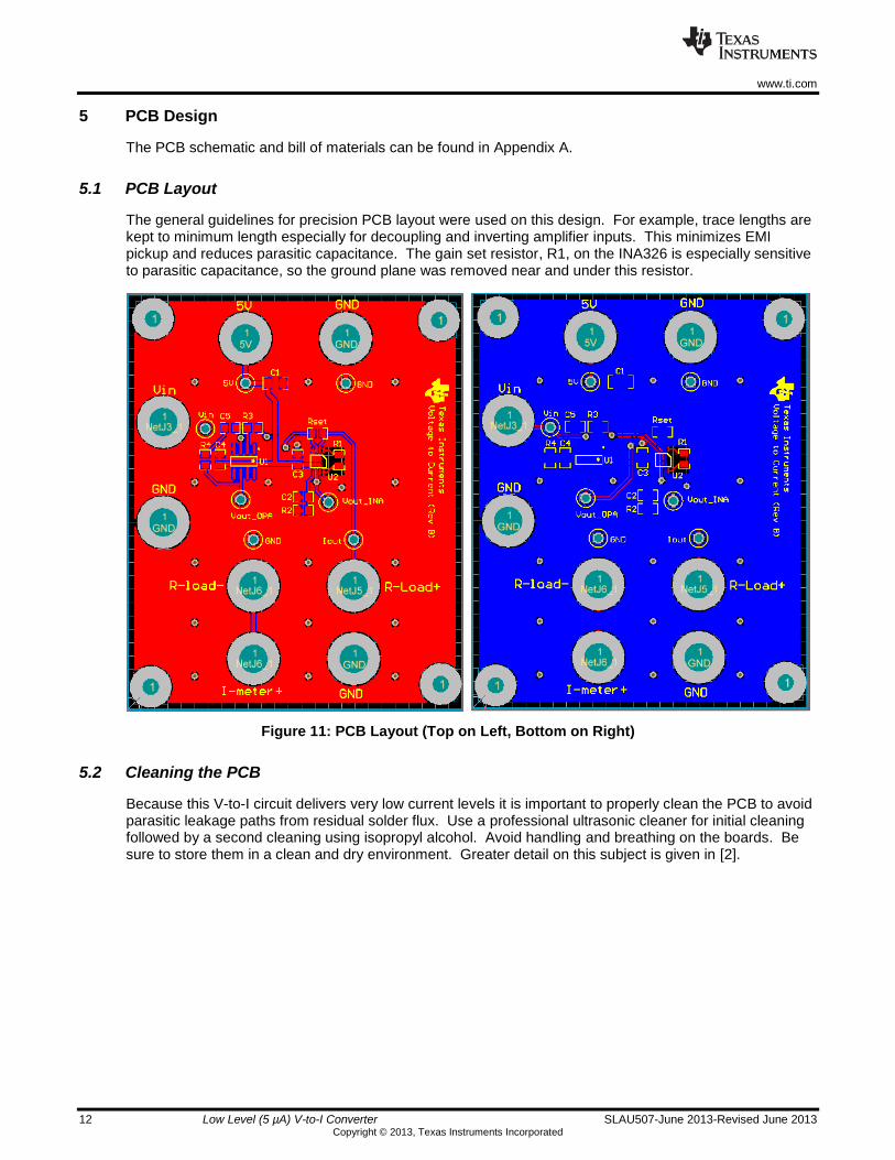
5.1 PCB Layout
The general guidelines for precision PCB layout were used on this design. For example, trace lengths are kept to minimum length especially for decoupling and inverting amplifier inputs. This minimizes EMI pickup and reduces parasitic capacitance. The gain set resistor, R1, on the INA326 is especially sensitive to parasitic capacitance, so the ground plane was removed near and under this resistor.
Figure 11: PCB Layout (Top on Left, Bottom on Right)
5.2 Cleaning the PCB
Because this V-to-I circuit delivers very low current levels it is important to properly clean the PCB to avoid parasitic leakage paths from residual solder flux. Use a professional ultrasonic cleaner for initial cleaning followed by a second cleaning using isopropyl alcohol. Avoid handling and breathing on the boards. Be sure to store them in a clean and dry environment. Greater detail on this subject is given in [2].

www.ti.com
SLAU507-June 2013-Revised June 2013 Low Level (5 µA) V-to-I Converter 13 Copyright © 2013, Texas Instruments Incorporated
6 Verification & Measured Performance
6.1 General precautions used in measuring low level V-to-I circuit
The objective of this circuit is to generate micro-amp level currents with accuracy and stability into the nano-amps. A high precision voltage source and ammeter has to be used to generate the input voltage and measure the output current of this circuit. Also, the V-to-I circuit board should be in a shielded environment to minimize noise pickup. Shielded cables (e.g. coax or shielded twisted pair) should be used to connect the test equipment to the V-to-I board. Figure 12 shows the test equipment setup used to measure the low current output.
6.5 digit precision voltage sourceMax Error 10uV on 10V range
6.5 digit precision ammeter Max Error 0.1nV on 10uA range
Low noise Linear Power Supply5V+/- 0.01V
Coax
Coax
Banana
Shielded Test environment
I-to-VPCB
Figure 12: Test Setup for V-to-I Board
www.ti.com
14 Low Level (5 µA) V-to-I Converter SLAU507-June 2013-Revised June 2013 Copyright © 2013, Texas Instruments Incorporated
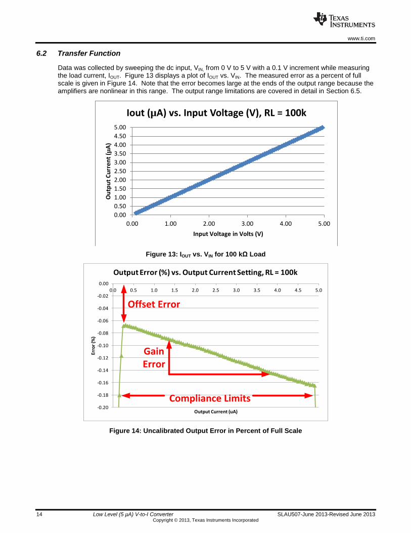
6.2 Transfer Function
Data was collected by sweeping the dc input, VIN, from 0 V to 5 V with a 0.1 V increment while measuring the load current, IOUT. Figure 13 displays a plot of IOUT vs. VIN. The measured error as a percent of full scale is given in Figure 14. Note that the error becomes large at the ends of the output range because the amplifiers are nonlinear in this range. The output range limitations are covered in detail in Section 6.5.
Figure 13: IOUT vs. VIN for 100 kΩ Load
-0.20
-0.18
-0.16
-0.14
-0.12
-0.10
-0.08
-0.06
-0.04
-0.02
0.00
0.0 0.5 1.0 1.5 2.0 2.5 3.0 3.5 4.0 4.5 5.0
Erro
r (%
)
Output Current (uA)
Output Error (%) vs. Output Current Setting, RL = 100k
Offset Error
Gain Error
Compliance Limits
Figure 14: Uncalibrated Output Error in Percent of Full Scale
0.00
0.50
1.00
1.50
2.00
2.50
3.00
3.50
4.00
4.50
5.00
0.00 1.00 2.00 3.00 4.00 5.00
Ou
tpu
t C
urr
en
t (µ
A)
Input Voltage in Volts (V)
Iout (µA) vs. Input Voltage (V), RL = 100k

www.ti.com
SLAU507-June 2013-Revised June 2013 Low Level (5 µA) V-to-I Converter 15 Copyright © 2013, Texas Instruments Incorporated
6.3 Calibration
The goal of this design is to obtain very accurate, stable, and repeatable output current vs. input voltage characteristics. The accuracy of this design is limited by resistor tolerance, INA gain accuracy, offset voltage and drift. A two point linear calibration can be used to obtain a highly accurate V-to-I converter. A two point linear calibration measures the slope and offset error on the transfer function. Using the equation for a straight line, we compute the slope (m) and the offset (b) using two points on the linear portion of the transfer function. Avoid using the end points of the function as the linearity becomes poor in these regions.
bxmy (5)
)xx(
)yy(m
12
12
(6)
22 xmyb (7)
m
byx
(8)
0.0
1.0
2.0
3.0
4.0
5.0
0.0 1.0 2.0 3.0 4.0 5.0
Cu
rre
nt
Ou
tpu
t (u
A)
Voltage Input (V)
Measured Current (uA)
(1.00000V, 1.00905uA) (4.00000V, 4.02752uA)
Figure 15: Measured current showing two points used in calibration
www.ti.com
16 Low Level (5 µA) V-to-I Converter SLAU507-June 2013-Revised June 2013 Copyright © 2013, Texas Instruments Incorporated
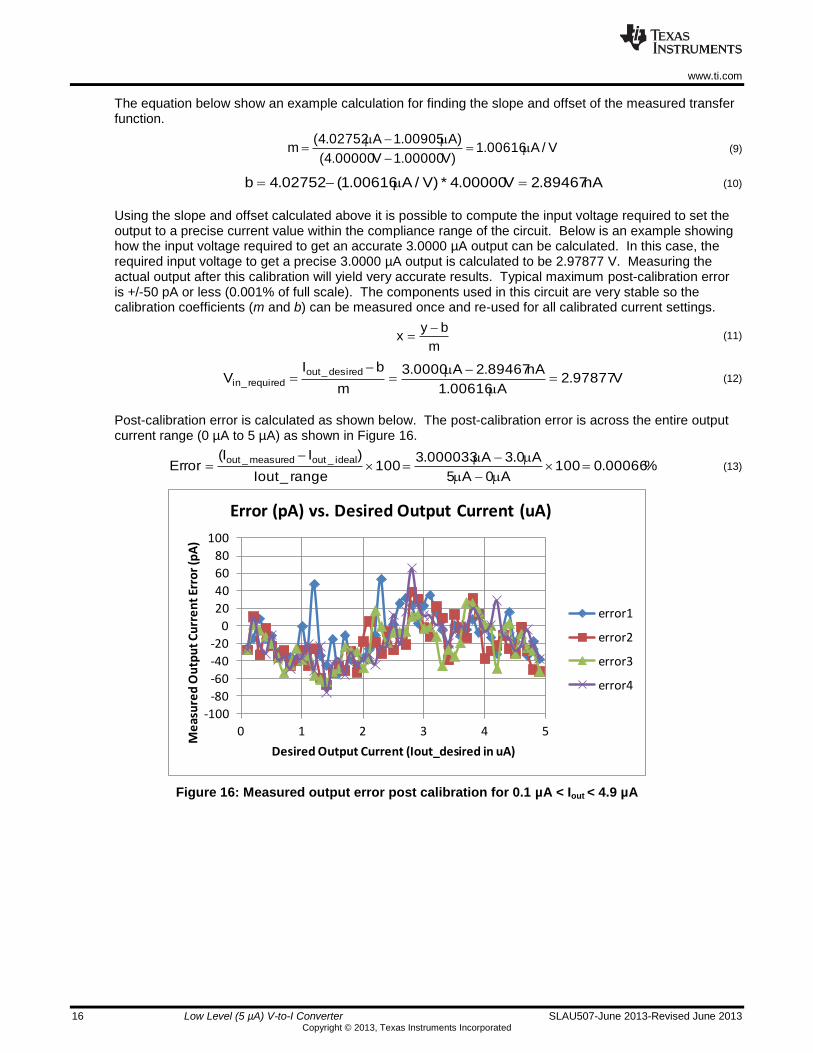
The equation below show an example calculation for finding the slope and offset of the measured transfer function.
V/A00616.1)V00000.1V00000.4(
)A00905.1A02752.4(m
(9)
nA89467.2V00000.4*)V/A00616.1(02752.4b (10)
Using the slope and offset calculated above it is possible to compute the input voltage required to set the output to a precise current value within the compliance range of the circuit. Below is an example showing how the input voltage required to get an accurate 3.0000 µA output can be calculated. In this case, the required input voltage to get a precise 3.0000 µA output is calculated to be 2.97877 V. Measuring the actual output after this calibration will yield very accurate results. Typical maximum post-calibration error is +/-50 pA or less (0.001% of full scale). The components used in this circuit are very stable so the calibration coefficients (m and b) can be measured once and re-used for all calibrated current settings.
m
byx
(11)
V97877.2A00616.1
nA89467.2A0000.3
m
bIV
desired_outrequired_in
(12)
Post-calibration error is calculated as shown below. The post-calibration error is across the entire output current range (0 µA to 5 µA) as shown in Figure 16.
%00066.0100A0A5
A0.3A000033.3100
range_Iout
)II(Error
ideal_outmeasured_out
(13)
Figure 16: Measured output error post calibration for 0.1 µA < Iout < 4.9 µA
-100
-80
-60
-40
-20
0
20
40
60
80
100
0 1 2 3 4 5
Me
asu
red
Ou
tpu
t C
urr
en
t Er
ror
(pA
)
Desired Output Current (Iout_desired in uA)
Error (pA) vs. Desired Output Current (uA)
error1
error2
error3
error4
www.ti.com
SLAU507-June 2013-Revised June 2013 Low Level (5 µA) V-to-I Converter 17 Copyright © 2013, Texas Instruments Incorporated
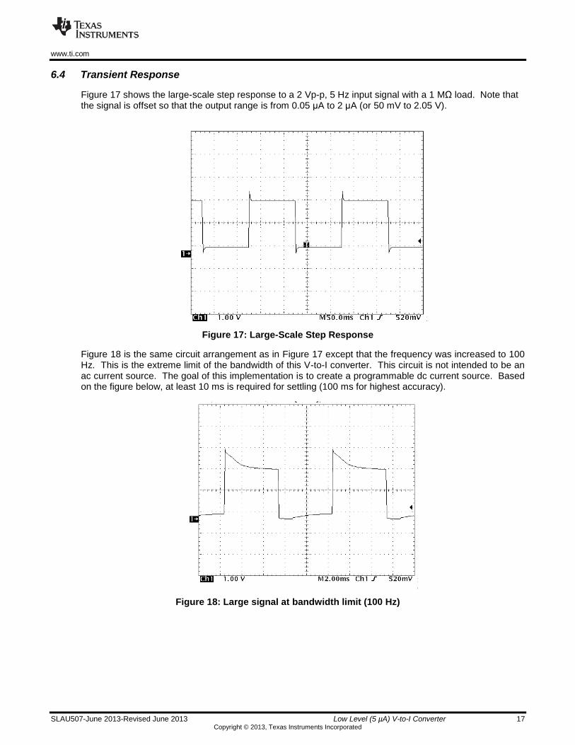
6.4 Transient Response
Figure 17 shows the large-scale step response to a 2 Vp-p, 5 Hz input signal with a 1 MΩ load. Note that the signal is offset so that the output range is from 0.05 μA to 2 μA (or 50 mV to 2.05 V).
Figure 17: Large-Scale Step Response
Figure 18 is the same circuit arrangement as in Figure 17 except that the frequency was increased to 100 Hz. This is the extreme limit of the bandwidth of this V-to-I converter. This circuit is not intended to be an ac current source. The goal of this implementation is to create a programmable dc current source. Based on the figure below, at least 10 ms is required for settling (100 ms for highest accuracy).
Figure 18: Large signal at bandwidth limit (100 Hz)
www.ti.com
18 Low Level (5 µA) V-to-I Converter SLAU507-June 2013-Revised June 2013 Copyright © 2013, Texas Instruments Incorporated
Figure 19 is the same arrangement as used in Figure 17 and Figure 18 except that a small (100 mVp-p) signal with a 500 mV dc offset was applied to the input. The objective of this test is to confirm the stability of the design. The design quickly settles to the final value with a properly damped response without overshoot or ringing. This is a good indication of circuit stability.
Figure 19: Small-Signal Stability
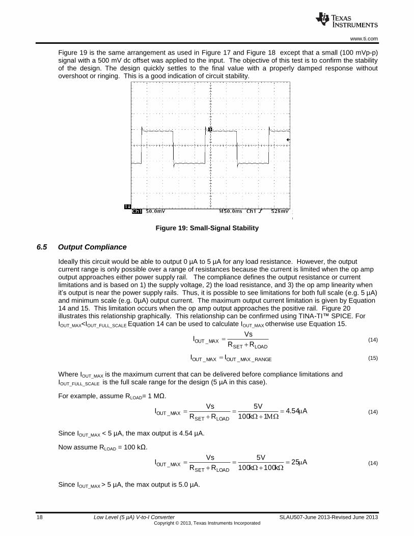
6.5 Output Compliance
Ideally this circuit would be able to output 0 µA to 5 µA for any load resistance. However, the output current range is only possible over a range of resistances because the current is limited when the op amp output approaches either power supply rail. The compliance defines the output resistance or current limitations and is based on 1) the supply voltage, 2) the load resistance, and 3) the op amp linearity when it’s output is near the power supply rails. Thus, it is possible to see limitations for both full scale (e.g. 5 µA) and minimum scale (e.g. 0µA) output current. The maximum output current limitation is given by Equation 14 and 15. This limitation occurs when the op amp output approaches the positive rail. Figure 20 illustrates this relationship graphically. This relationship can be confirmed using TINA-TI™ SPICE. For IOUT_MAX<IOUT_FULL_SCALE Equation 14 can be used to calculate IOUT_MAX otherwise use Equation 15.
LOADSETMAX_OUT
RR
VsI
(14)
RANGE_MAX_OUTMAX_OUT II (15)
Where IOUT_MAX is the maximum current that can be delivered before compliance limitations and IOUT_FULL_SCALE is the full scale range for the design (5 µA in this case).
For example, assume RLOAD= 1 MΩ.
A54.41k100
V5
RR
VsI
LOADSETMAX_OUT
(14)
Since IOUT_MAX < 5 µA, the max output is 4.54 µA.
Now assume RLOAD = 100 kΩ.
A25k100k100
V5
RR
VsI
LOADSETMAX_OUT
(14)
Since IOUT_MAX > 5 µA, the max output is 5.0 µA.
www.ti.com
SLAU507-June 2013-Revised June 2013 Low Level (5 µA) V-to-I Converter 19 Copyright © 2013, Texas Instruments Incorporated
Figure 20: Maximum Output vs. Load Resistance
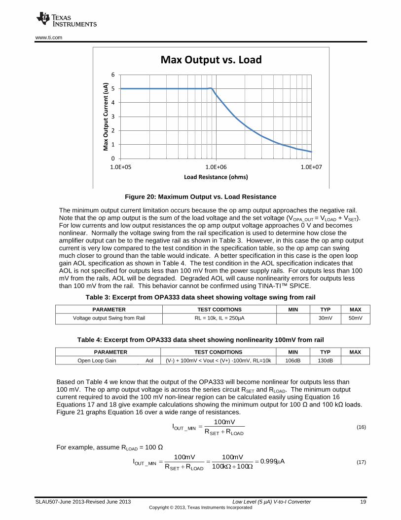
The minimum output current limitation occurs because the op amp output approaches the negative rail. Note that the op amp output is the sum of the load voltage and the set voltage (VOPA_OUT = VLOAD + VSET). For low currents and low output resistances the op amp output voltage approaches 0 V and becomes nonlinear. Normally the voltage swing from the rail specification is used to determine how close the amplifier output can be to the negative rail as shown in Table 3. However, in this case the op amp output current is very low compared to the test condition in the specification table, so the op amp can swing much closer to ground than the table would indicate. A better specification in this case is the open loop gain AOL specification as shown in Table 4. The test condition in the AOL specification indicates that AOL is not specified for outputs less than 100 mV from the power supply rails. For outputs less than 100 mV from the rails, AOL will be degraded. Degraded AOL will cause nonlinearity errors for outputs less than 100 mV from the rail. This behavior cannot be confirmed using TINA-TI™ SPICE.
Table 3: Excerpt from OPA333 data sheet showing voltage swing from rail
PARAMETER TEST CODITIONS MIN TYP MAX
Voltage output Swing from Rail RL = 10k, IL = 250µA 30mV 50mV
Table 4: Excerpt from OPA333 data sheet showing nonlinearity 100mV from rail
PARAMETER TEST CONDITIONS MIN TYP MAX
Open Loop Gain Aol (V-) + 100mV < Vout < (V+) -100mV, RL=10k 106dB 130dB
Based on Table 4 we know that the output of the OPA333 will become nonlinear for outputs less than 100 mV. The op amp output voltage is across the series circuit RSET and RLOAD. The minimum output current required to avoid the 100 mV non-linear region can be calculated easily using Equation 16 Equations 17 and 18 give example calculations showing the minimum output for 100 Ω and 100 kΩ loads. Figure 21 graphs Equation 16 over a wide range of resistances.
LOADSETMIN_OUT
RR
mV100I
(16)
For example, assume RLOAD = 100 Ω
A999.0100k100
mV100
RR
mV100I
LOADSETMIN_OUT
(17)
0
1
2
3
4
5
6
1.0E+05 1.0E+06 1.0E+07
Max
Ou
tpu
t C
urr
en
t (u
A)
Load Resistance (ohms)
Max Output vs. Load

www.ti.com
20 Low Level (5 µA) V-to-I Converter SLAU507-June 2013-Revised June 2013 Copyright © 2013, Texas Instruments Incorporated
For example, assume RLOAD = 100 kΩ
A5.0
k100k100
mV100
RR
mV100I
LOADSETMAX_OUT
(18)
Figure 21: Minimum Output for Highest Accuracy
0
0.2
0.4
0.6
0.8
1
1.2
1.E+02 1.E+03 1.E+04 1.E+05 1.E+06
Iou
t in
uA
Load Resistance in Ohms
Minimum output for highest accuracy

www.ti.com
SLAU507-June 2013-Revised June 2013 Low Level (5 µA) V-to-I Converter 21 Copyright © 2013, Texas Instruments Incorporated
The 100 mV limitation is a guideline for highest accuracy. The actual amplifier performance will generally be better than the expected limitations. Figure 22 shows the measured output error for a 50 kΩ load for four different measurement runs. The error for low output currents (i.e. 0 µA to 50 µA) is high compared with the error across the remainder of the range. This is because of the 100 mV minimum output limitation. The measured results correspond well with the theoretical results given in Figure 22.
Figure 22: Post calibration error showing nonlinearity error for low op amp outputs
Normal Post Cal Error ± 0.1pA
Nonlinear Region
Zoom in on error

www.ti.com
22 Low Level (5 µA) V-to-I Converter SLAU507-June 2013-Revised June 2013 Copyright © 2013, Texas Instruments Incorporated
Figure 23 shows measured results that confirm that the output compliance to ground improves with heavy loads. The limitations shown in Figure 22 correlate with the minimum output limitations given in Figure 21.
-1.0
-0.5
0.0
0.5
1.0
0.00 0.20 0.40 0.60 0.80 1.00
Erro
r (n
A)
Output Current (uA)
Error (nA) 500k Load
-1.0
-0.5
0.0
0.5
1.0
0.00 0.20 0.40 0.60 0.80 1.00
Erro
r (n
A)
Output Current (uA)
Error (nA) 50k Load
VOPA = 0.12V
VOPA = 0.075V
Figure 23: Larger loads have better minimum output compliance limitations
6.6 Measured Result Summary
The final summary comparing measured and simulated results to the goals is given in Table 5.
Table 5: Comparison of Design Goal, Simulation, and Measured Performance
Goal Simulated Measured
Uncalibrated Accuracy (%FSR) 0.2% 0.3% 0.18%
Calibrated Accuracy (%FSR) 0.01% na 0.001%
Load Compliance 0<R<500 kΩ
Max Linear Output (µA) 4.0 µA 4.9 µA 4.9 µA
Load Compliance 0<R<500 kΩ
Min Linear Output (µA) 1.0 µA 0 µA 0.6 µA

www.ti.com
SLAU507-June 2013-Revised June 2013 Low Level (5 µA) V-to-I Converter 23 Copyright © 2013, Texas Instruments Incorporated
7 Modifications
7.1 Selecting different amplifiers
The components selected for this design were based on the design goals outlined at the beginning of the design process. Selecting a chopper-stabilized amplifier such as the OPA333 removes most of the dc errors and drift normally attributed to the amplifier in this design. Calibration can be used to obtain the highest accuracy.
Table 6: Brief Comparison of Amplifiers
Amplifier Max Supply Voltage (V)
Max Offset Voltage (µV)
Max Offset Drift (µV/C)
Bandwidth (MHz) Quiescent
Current (µA)
OPA333 5.5 10 0.05 0.35 34
OPA335 5.5 5 0.05 2 700
OPA320 5.5 150 5 20 1600
OPA735 12 5 0.05 1.6 1500
OPA188 36 25 0.085 1 950
7.2 Selecting different gain
The gain of the instrumentation amplifier was set to a gain of 10 V/V to improve the compliance. For a full scale input of 5 V the voltage across the set resistor is 0.5 V which allows for load voltages up to 4.5 V. Unfortunately, using a gain of 10 V/V will degrade the performance when low resistance loads are driven by low current levels (e.g. 100 Ω x 0.1 µA). In this case the overall output voltage from the op amp is near ground and it becomes non-linear (e.g. VOPA = VSET + VLOAD = 0.01 V + 10 µV = 0.01 V).
A lower gain (e.g. GINA = 1 V/V) can be used in the case that low value resistance loads are driven by low current levels. For example, if a 100 µA load is driven by a 0.1 µA current the op amp output voltage will be about 0.1 V. However, making this change will degrade the compliance for larger loads.
7.3 Selecting different current output range
Many of the difficulties in achieving a high degree of accuracy in this design relate to low current design. For example, the careful and thorough cleaning of the board is needed because we are attempting to get a microamp signal that is stable out to nanoamps. If the output range of the circuit is scaled for higher output current (e.g. 100 µA), then special attention to low current considerations (e.g. cleaning) will not be as critical. On the other hand, if the output is scaled for lower current (e.g. 100 nA), then other special low current techniques may be needed to achieve the highest accuracy. For example, an ultra-low current reference may require guarding, low triboelectric effect cables, special materials, special precision resistors, and many other precautions.
7.4 Dual Supply Version
This circuit can be easily modified for dual supply operation. The advantage of the dual supply configuration is that it can both source and sink current.

www.ti.com
24 Low Level (5 µA) V-to-I Converter SLAU507-June 2013-Revised June 2013 Copyright © 2013, Texas Instruments Incorporated
8 About the Author
Arthur Kay is an applications engineering manager at TI where he specializes in the support of amplifiers, references, and mixed signal devices. Arthur focuses a good deal on industrial applications such as bridge sensor signal conditioning. Arthur has published a book and an article series on amplifier noise. Arthur received his M.S.E.E. from Georgia Institute of Technology, and B.S.E.E. from Cleveland State University.
9 Acknowledgements & References
1. Green, T., Operational Amplifier Stability, Parts 1 – 11, November 2008, http://www.en-genius.net/site/zones/acquisitionZONE/technical_notes/acqt_050712
2. Grohe, P., Design femtoampere circuits with low leakage, Parts 1 – 3, November 2011, http://www.edn.com/design/analog/4368681/Design-femtoampere-circuits-with-low-leakage-part-one?page=3
3. Low Level Measurements Handbook, Sixth Edition, Keithley Instruments, 2004
www.ti.com
SLAU507-June 2013-Revised June 2013 Low Level (5 µA) V-to-I Converter 25 Copyright © 2013, Texas Instruments Incorporated
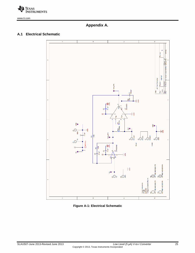
Appendix A.
A.1 Electrical Schematic
Figure A-1: Electrical Schematic

www.ti.com
26 Low Level (5 µA) V-to-I Converter SLAU507-June 2013-Revised June 2013 Copyright © 2013, Texas Instruments Incorporated
A.2 Bill of Materials
Item Qty Value Designator Description Manufacturer Manufacturer Part No. DigiKey PartNumber
1 1 4.7uF C1 CAP, CERM, 4.7uF, 16V, +/-20%,
X7R, 1206 TDK C3216X5R1H475K160AB 445-5994-1-ND
2 1 1000pF C2 CAP, CERM, 1000pF, 50V, +/-1%,
C0G/NP0, 0805 AVX 08055A102FAT2A 478-3759-1-ND
3 3 0.1uF C3, C4, C5 CAP, CERM, 0.1uF, 50V, +/-5%, X7R,
0805 AVX 08055C104JAT2A 478-3352-1-ND
4 4
MACHINE SCREW PAN PHILLIPS 4-40
B&F Fastener PMS 440 0038 PH H782-ND
5 4
H1, H2, H3, H4
STANDOFF HEX 4-40THR ALUM .500"L
Keystone 2203 2203K-ND
6 8
J1, J2, J3, J4, J5, J6,
J7, J8
Standard Banana Jack, Uninsulated, 5.5mm
Keystone 575-4 5-4K-ND
7 1 40.2k R1 RES, 40.2k ohm, 0.1%, 0.125W,
0805 TE
Connectivity 676335-2 A102342CT-ND
8 1 200k R2 RES, 200k ohm, 0.1%, 0.125W,
0805 TE
Connectivity 4-1676971-2 A102090CT-ND
9 2 100k R3, R4 RES, 100k ohm, 1%, 0.125W, 0805 Vishay-Dale CRCW0805100KFKEA 541-100KCCT-ND
10 1 1.00Meg Rset RES, 1.00Meg ohm, 1%, 0.125W,
0805 Vishay-Dale CRCW08051M00FKEA 541-1.00MCCT-ND
11 2
TP1, TP7 Test Point, TH, Compact, Black Keystone 5124 5001K-ND
12 1
TP2 Test Point, TH, Compact, Red Keystone 5005 5005K-ND
13 1
TP3, TP4, TP5, TP6
Test Point, TH, Compact, Purple Keystone 5124 5124K-ND
14 1
U1 Single JFET Input Op Amp Texas
Instruments OPA333AID 296-19545-5-ND
15 1
U2 IC OPAMP INSTR R-R 1KHZ 8VSSOP Texas
Instruments INA326EA/2K5 INA326EA/2K5CT-ND
Figure A-2: Bill of Materials
IMPORTANT NOTICE FOR TI REFERENCE DESIGNS
Texas Instruments Incorporated ("TI") reference designs are solely intended to assist designers (“Buyers”) who are developing systems thatincorporate TI semiconductor products (also referred to herein as “components”). Buyer understands and agrees that Buyer remainsresponsible for using its independent analysis, evaluation and judgment in designing Buyer’s systems and products.
TI reference designs have been created using standard laboratory conditions and engineering practices. TI has not conducted anytesting other than that specifically described in the published documentation for a particular reference design. TI may makecorrections, enhancements, improvements and other changes to its reference designs.
Buyers are authorized to use TI reference designs with the TI component(s) identified in each particular reference design and to modify thereference design in the development of their end products. HOWEVER, NO OTHER LICENSE, EXPRESS OR IMPLIED, BY ESTOPPELOR OTHERWISE TO ANY OTHER TI INTELLECTUAL PROPERTY RIGHT, AND NO LICENSE TO ANY THIRD PARTY TECHNOLOGYOR INTELLECTUAL PROPERTY RIGHT, IS GRANTED HEREIN, including but not limited to any patent right, copyright, mask work right,or other intellectual property right relating to any combination, machine, or process in which TI components or services are used.Information published by TI regarding third-party products or services does not constitute a license to use such products or services, or awarranty or endorsement thereof. Use of such information may require a license from a third party under the patents or other intellectualproperty of the third party, or a license from TI under the patents or other intellectual property of TI.
TI REFERENCE DESIGNS ARE PROVIDED "AS IS". TI MAKES NO WARRANTIES OR REPRESENTATIONS WITH REGARD TO THEREFERENCE DESIGNS OR USE OF THE REFERENCE DESIGNS, EXPRESS, IMPLIED OR STATUTORY, INCLUDING ACCURACY ORCOMPLETENESS. TI DISCLAIMS ANY WARRANTY OF TITLE AND ANY IMPLIED WARRANTIES OF MERCHANTABILITY, FITNESSFOR A PARTICULAR PURPOSE, QUIET ENJOYMENT, QUIET POSSESSION, AND NON-INFRINGEMENT OF ANY THIRD PARTYINTELLECTUAL PROPERTY RIGHTS WITH REGARD TO TI REFERENCE DESIGNS OR USE THEREOF. TI SHALL NOT BE LIABLEFOR AND SHALL NOT DEFEND OR INDEMNIFY BUYERS AGAINST ANY THIRD PARTY INFRINGEMENT CLAIM THAT RELATES TOOR IS BASED ON A COMBINATION OF COMPONENTS PROVIDED IN A TI REFERENCE DESIGN. IN NO EVENT SHALL TI BELIABLE FOR ANY ACTUAL, SPECIAL, INCIDENTAL, CONSEQUENTIAL OR INDIRECT DAMAGES, HOWEVER CAUSED, ON ANYTHEORY OF LIABILITY AND WHETHER OR NOT TI HAS BEEN ADVISED OF THE POSSIBILITY OF SUCH DAMAGES, ARISING INANY WAY OUT OF TI REFERENCE DESIGNS OR BUYER’S USE OF TI REFERENCE DESIGNS.
TI reserves the right to make corrections, enhancements, improvements and other changes to its semiconductor products and services perJESD46, latest issue, and to discontinue any product or service per JESD48, latest issue. Buyers should obtain the latest relevantinformation before placing orders and should verify that such information is current and complete. All semiconductor products are soldsubject to TI’s terms and conditions of sale supplied at the time of order acknowledgment.
TI warrants performance of its components to the specifications applicable at the time of sale, in accordance with the warranty in TI’s termsand conditions of sale of semiconductor products. Testing and other quality control techniques for TI components are used to the extent TIdeems necessary to support this warranty. Except where mandated by applicable law, testing of all parameters of each component is notnecessarily performed.
TI assumes no liability for applications assistance or the design of Buyers’ products. Buyers are responsible for their products andapplications using TI components. To minimize the risks associated with Buyers’ products and applications, Buyers should provideadequate design and operating safeguards.
Reproduction of significant portions of TI information in TI data books, data sheets or reference designs is permissible only if reproduction iswithout alteration and is accompanied by all associated warranties, conditions, limitations, and notices. TI is not responsible or liable forsuch altered documentation. Information of third parties may be subject to additional restrictions.
Buyer acknowledges and agrees that it is solely responsible for compliance with all legal, regulatory and safety-related requirementsconcerning its products, and any use of TI components in its applications, notwithstanding any applications-related information or supportthat may be provided by TI. Buyer represents and agrees that it has all the necessary expertise to create and implement safeguards thatanticipate dangerous failures, monitor failures and their consequences, lessen the likelihood of dangerous failures and take appropriateremedial actions. Buyer will fully indemnify TI and its representatives against any damages arising out of the use of any TI components inBuyer’s safety-critical applications.
In some cases, TI components may be promoted specifically to facilitate safety-related applications. With such components, TI’s goal is tohelp enable customers to design and create their own end-product solutions that meet applicable functional safety standards andrequirements. Nonetheless, such components are subject to these terms.
No TI components are authorized for use in FDA Class III (or similar life-critical medical equipment) unless authorized officers of the partieshave executed an agreement specifically governing such use.
Only those TI components that TI has specifically designated as military grade or “enhanced plastic” are designed and intended for use inmilitary/aerospace applications or environments. Buyer acknowledges and agrees that any military or aerospace use of TI components thathave not been so designated is solely at Buyer's risk, and Buyer is solely responsible for compliance with all legal and regulatoryrequirements in connection with such use.
TI has specifically designated certain components as meeting ISO/TS16949 requirements, mainly for automotive use. In any case of use ofnon-designated products, TI will not be responsible for any failure to meet ISO/TS16949.
Mailing Address: Texas Instruments, Post Office Box 655303, Dallas, Texas 75265Copyright © 2013, Texas Instruments Incorporated