c onf with integrated host processor set top box backend decoder
TRANSCRIPT

This is advance information on a new product now in development or undergoing evaluation. Details are subject to change without notice
7110123 B
CONFIDENTIAL®
SET TOP BOX BACKEND DECODERWITH INTEGRATED HOST PROCESSOR
STi5512
PRODUCT PREVIEW
High performance graphics system• High resolution chroma mode (4:4:4) for RGB output• 2 to 8 bits per pixel OSD options• Link list control• 4-bit mixing factor by region or 6-bit mixing for each
CLUT entry (anti-aliasing)• 8-bit Y, U and V resolution palette• Extra YUV plane for background images or graphics• 2D, paced BLT engine with “fill” function• Anti-flicker and anti-flutter filters
Enhanced 32-bit VL-RISC CPU - 60 MHz clock• Fast integer/bit operation and very high code density
High performance memory/cache subsystem• 2 Kbytes instruction cache, 2 Kbytes data cache or
SRAM, 4 Kbytes SRAM• 200 Mbytes/s maximum bandwidth
Combined video and audio decoder core• Video decoder fully supports MPEG-2 MP@ML.
Letter box (16:9 and 14:9), 2:1, 3:1, 4:1 downsizing• Memory reduction - PAL MP@ML in 12 Mbits• Audio decoder supports layers 1 and 2 of MPEG 1,
and an AC-3 interface to an external decoder• Digital YCrCb output in 4:2:2 format
PAL/NTSC/SECAM encoder• Outputs RGB with 10-bit DACs and CVBS, Y, C and
component output (YUV) with 10-bit DACS• Separate OSD control for RGB and CVBS outputs• Genlock support
High performance SDRAM memory interface• Supports two 16- or one 64-Mbit 100 MHz SDRAMs• Accessible by MPEG decoder, PTI, DMAs and CPU• High bandwidth access from CPU allows high
performance OSD operations Programmable external memory interface (EMI)
• Support for SDRAM included Programmable transport interface
• Parallel or serial input• Supports DVB bit-streams• More than 32 PIDs supported• DVB descrambler• 32 SI/PSI filters of 8 bytes
Vectored interrupts - 8 prioritized levels Interfaces and DMA engines
• 2 SmartCard interfaces, 2 UARTs, 2 I2C / SPI controllers, 3 PWM outputs, 4 timers, 3 capture timers
• Block move DMA• Teletext interface, input from external source• IEEE 1284 port, or IEEE 1394 A/V link layer
interface Low power controller/real time clock/watchdog
JTAG Test Access Port Professional toolset support
• ANSI C compiler and libraries• Advanced debugging tools
Non-intrusive debug controller• Hardware breakpoints• Real time trace
APPLICATIONS Set top boxes to DVB standards.
SRAM
Block moveDMA
Programmabletransportinterface
EMI
4 Kbytes
ST20CPU
2 Kbytes
cacheand 2 Kbytesdata cache
IEEE 1394link layerinterface
IEEE 1284interface
Interruptcontroller
2 SmartCardinterfaces
Teletextinterface
Diagnosticcontroller
1 OS-Link2 UARTs
2 I2C
instruction
and systemservices
(ASC)
3 PWM
MPEGaudio andexternal
decoder I/F
MPEGvideo
decoder
PAL/NTSC
encoder/SECAM
SRAM
10 June 1999

L STi5512
CONFIDENTIA1 IntroductionThe STi5512 is one of the OMEGA family of integrated multimedia decoder engines for DVB set top box systems. It offers a high level of integration by reducing the complete set-top box decoding chain from transport demultiplexing to PAL/NTSC/SECAM encoder onto one chip. At the same time it dramatically enhances CPU and graphics performance, and cuts down total system memory cost.
The STi5512 integrates the functions of the MPEG decoder and the PAL/NTSC/SECAM encoder. This single device includes the following subsystems, which are described in more detail below:
• A transport demultiplexor,
• A system microcontroller,
• A MPEG audio decoder,
• A MPEG video decoder,
• A PAL/NTSC/SECAM encoder.
The STi5512 minimizes system costs. The external memory interface module (EMI) contains a zero glue logic DRAM/SDRAM controller and a low cost 32/16/8-bit EPROM interface. SDRAM is supported at the CPU clock rate, 60 MHz.
The SDRAM memory interface directly supports two 16-Mbit or one 64-Mbit 100MHz SDRAM providing the very high bandwidths to support MPEG decoding and display, on-screen display (OSD) drawing and display, and general system use. Furthermore the ST20 VL-RISC micro-core has the highest code density of any 32-bit CPU, leading to the lowest cost program ROM.
The STi5512 is supported by a range of software and hardware development tools for PC and UNIX hosts including an ANSI-C ST20 software toolset and the ST20 window based debugging toolkit.
Display
The STi5512 provides an enhanced range of display functions and features to improve the video display and add background and foreground graphics and pictures. Features include:
• Five display planes - background color, still picture, decompressed video, on-screen display and sub-picture,
• Letterbox filtering,
• Anti-flutter and anti-flicker filters,
• 2- to 8-bits per pixel on-screen display with 24-bit color with anti-aliasing,
• Hardware cursor option,
• Display memory expandable to 64 Mbits of SDRAM,
• 2D BLT block move engine,
• Two additional display modes for full resolution source video using Frame based filtering for Luma and Chroma.
Video decoder
The video decoder fully supports MPEG-2 Main Profile/Main Level (MP@ML), and has the following features:
• A memory reduction architecture, allowing sharing of a single 16-Mbit SDRAM between MPEG decoding, micro and transport functions.
2/23 7110123 B

LSTi5512
CONFIDENTIAPAL/NTSC/SECAM encoder with teletext and closed caption
The on-chip digital encoder provides analog video output to PAL, NTSC and SECAM standards, with the following features:
• RGB and YUV outputs:
• CVBS, Y, C outputs,
• Close caption,
• Double DENC function,
• Support for placement of teletext, WSS (wide screen signalling) and VPS on any line,
• VBI insertion in square pixel mode,
• Genlock support for locking to external source and display of OSD over analogue source using SCART fast switch facility.
Transport demultiplexor
The STi5512 Programmable Transport Interface features:
• Inputs from a LinkIC or IEEE 1394 link layer controller
• A DVB Descrambler
• Demultiplexing of transport stream by PID
• Section filtering
• DMA and buffering of streams in memory
MPEG audio decoder
The STi5512 incorporates a 2-channel MPEG-1 audio decoder, with an interface for connection to external audio decoders. The audio decoder supports layer I and layer II.
System microcontroller
The STi5512 incorporates a ST20-C2 CPU. The ST20 micro-core family has been developed by STMicroelectronics to provide the tools and building blocks to enable the development of highly integrated application specific 32-bit devices at the lowest cost and fastest time to market. The ST20 macrocell library includes the ST20Cx family of 32-bit VL-RISC (variable length reduced instruction set computer) micro-cores, embedded memories, standard peripherals, I/O, controllers and ASICs. The STi5512 32-bit VL-RISC for host functions and application code runs at up to 60 MHz.
The performance offered by the ST20 32-bit micro-core allows the following operations to be performed in software:
• Device drivers and synchronization
• System management functions
• Electronic program guide and user interface
• Conditional access control
• Interpretation and execution of loadable application programs
The use of a 32-bit CPU enables advanced graphics routines to be employed for on-screen display functions, allowing fast turnaround of system upgrades. Source code software licences are available from STMicroelectronics for items 1 and 2 in the list above, and a library of graphics functions to assist with the Electronic program guide and user interface.
7110123 B 3/23
L STi5512
CONFIDENTIAThe STi5512 uses the ST20 macrocell library to provide all of the peripheral hardware modules required. These include:
• High performance internal SRAM and cache subsystem
• I2C interfaces to other devices in the set top box
• Interrupt controller for internal and external interrupts
• Programmable memory interface supporting ROM, SRAM and DRAM/SDRAM. SDRAM is supported at the CPU clock rate, 60 MHz.
• PWM/timer module for control of system clock VCXOs
• Programmable I/O pins
• UART serial I/O interface to modem and auxiliary ports - including hardware handshake
• Smart card interfaces including the ability to use the 16 byte transmit and receive FIFOs
4/23 7110123 B
LSTi5512
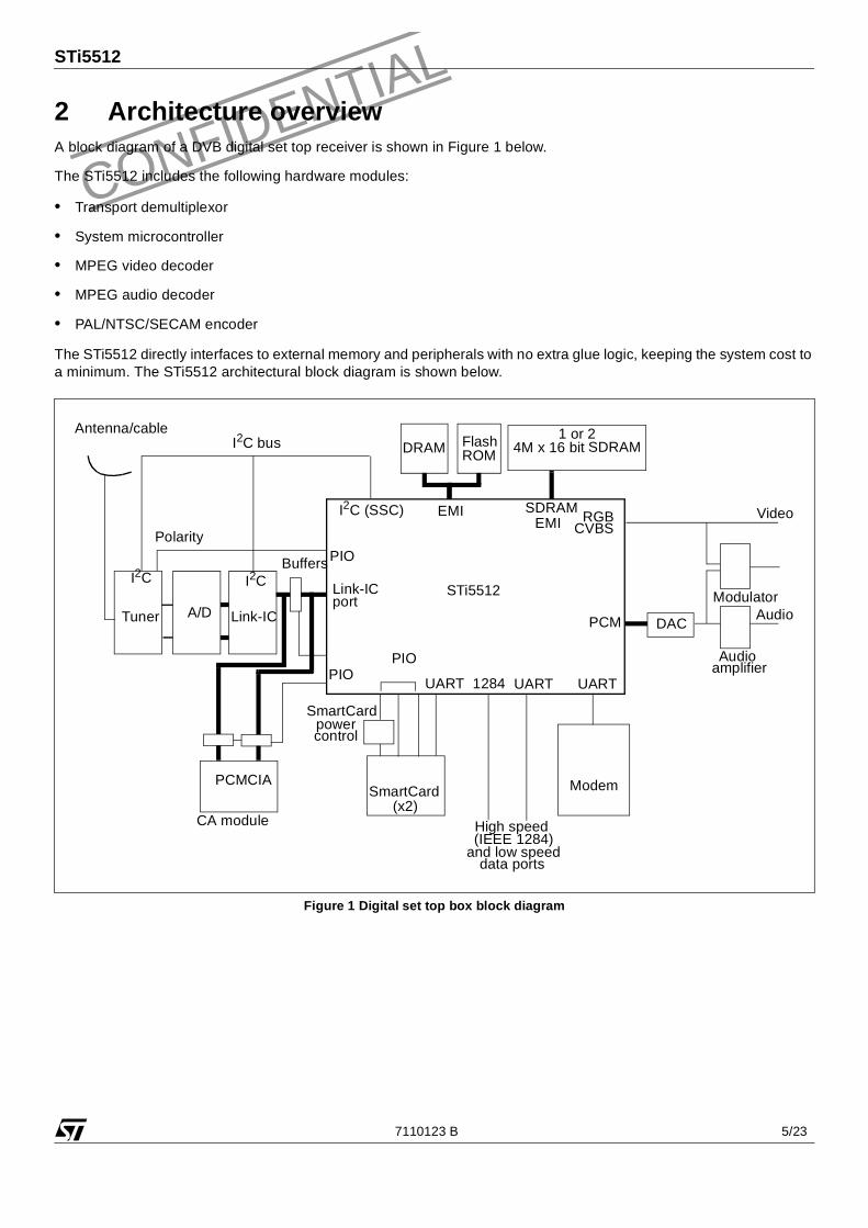
CONFIDENTIA2 Architecture overviewA block diagram of a DVB digital set top receiver is shown in Figure 1 below.
The STi5512 includes the following hardware modules:
• Transport demultiplexor
• System microcontroller
• MPEG video decoder
• MPEG audio decoder
• PAL/NTSC/SECAM encoder
The STi5512 directly interfaces to external memory and peripherals with no extra glue logic, keeping the system cost to a minimum. The STi5512 architectural block diagram is shown below.
Figure 1 Digital set top box block diagram
STi5512
DAC
Audio
Link-ICport Modulator
Tuner
I2C bus
SmartCard
Audio
UARTUART
I2C (SSC)
I2C
Video
amplifierUART
PIO
A/D
Antenna/cable
High speed
and low speed
Flash 1 or 2SDRAM
ROMDRAM
Modem
powercontrol
PIO
Link-IC
I2CBuffersPIO
CA module
Polarity
EMI RGBCVBS
PCM
SDRAMEMI
data ports
(IEEE 1284)
1284
4M x 16 bit
(x2)
PCMCIASmartCard
7110123 B 5/23

L STi5512
CONFIDENTIA
Figure 2 STi5512 architecture block diagram
SRAM
Block moveDMA
Programmabletransportinterface
EMI
4 Kbytes
ST20CPU
2 Kbytes
cacheand 2 Kbytesdata cache
IEEE 1394link layerinterface
IEEE 1284interface
Interruptcontroller
2 SmartCardinterfaces
Teletextinterface
Diagnosticcontroller
1 OS-Link2 UARTs
2 I2C
instruction
and systemservices
3 PWM
(ASC)
MPEGaudio andexternal
decoder I/F
MPEGvideo
decoder
PAL/NTSC/
encoderSECAM
6/23 7110123 B
LSTi5512
CONFIDENTIA2.1 STi5512 functional modules
STi5512 architecture block diagram on page 6 shows the subsystem modules that comprise the STi5512. These modules are outlined below.
Processor
The Central Processing Unit (CPU) on the STi5512 is the enhanced ST20-C2 32-bit processor core running at 60 MHz clock rate. It contains instruction processing logic, instruction and data pointers, and an operand register. It directly accesses the high speed on-chip caches and SRAM, which can store data or programs. The processor can also access memory via the External Memory Interface (EMI) and SDRAM interface.
MPEG-2 video and MPEG-1 audio decoder subsystems
This subsystem takes the MPEG compressed data streams and decompresses them, outputting digital YUV data in the case of the video decoder, and stereo PCM samples in the case of the audio decoder. The decoded video is fed to the display subsystem. An interface is provided to output an audio bit-stream for decoding by an external MPEG or AC-3 decoder to support multi-channel (surround) audio.
The video decoder implemented on the STi5512 uses a patented memory reduction/bandwidth reduction scheme to offer the user the best compromise between bandwidth and memory size. The algorithm is lossless and uses “on-the-fly” decoding to reduce the memory requirements to two frame buffers in memory size reduction mode. When used in bandwidth reduction mode, the memory usage is the normal three buffers, but the bandwidth required by the decoder is significantly reduced over a classical implementation.
The SDRAM interface includes all the signals necessary for control of the memory. Refresh is handled automatically by the decoder. The SDRAM interface supports two 16-Mbit or one 64-Mbit 100 MHz SDRAMs. The memory is used to hold the bit buffer, store decoded pictures and provide the display buffer. It also holds the user-defined on-screen display (OSD) bitmaps and can be used by the CPU for private storage of data. For the decoding of PAL MP@ML sequences, 12 Mbits of SDRAM are required.
Figure 3 Display planes
France
Backgroundcolor
Stillpictureplane
On-screen display
08:23pm
Replay Score Stats
France
France
Replay Score Stats
Cursor on sub-picture plane
Sub-picture optional positions
08:23pm
Replay Score Stats
08:23pm
Decompressedvideo
7110123 B 7/23
L STi5512
CONFIDENTIAGraphics and display subsystem
The display unit is part of the MPEG video decoder. It can overlay several display planes, as shown in Figure 3 on page 7.
It takes the decompressed MPEG video data and performs the following functions:
• Optionally perform horizontal resampling of both luminance and chrominance data
• Reconstruct vertical data to create 4:2:2 sample format
• Generate on-screen display bit map for superposition onto picture output
• Allow sub-picture decoder output to be mixed onto picture output
• Optionally perform anti-flicker and anti-flutter filtering
• Optionally perform vertical resampling of both luminance and chrominance data
• Still picture plane with graphics capability
• 2D block move to copy rectangular sections of the display
• 4:4:4 chroma resolution for RGB output.
• 4:2:2 chroma resolution for CVBS output
• Separate control on OSD between CVBS and YC on one hand and RGB and YUV on the other
The sub-picture decoder can also be used as a hardware cursor unit. The priority of the sub-picture is first raised by programming a register so it is above all the other display planes. A cursor can be defined using an optionally compressed (run-length encoded) bitmap stored in external SDRAM. The bitmap can be any size up to a full screen. Per-pixel alpha-blending factors can be defined for each cursor to provide anti-aliasing with the background. The cursor is then moved around using register writes into X and Y coordinate registers.
The digital video data is fed to the PAL/NTSC/SECAM encoder subsystem.
PAL/NTSC/SECAM encoder
Integrated into this subsystem is all the digital processing and the digital to analog convertors required to process the digital video output from the MPEG video decoder and produce RGB, YUV, YC and CVBS analog outputs. The output of the teletext interface is filtered and re-inserted into the blanking interval in this subsystem.
Programmable Transport Interface
The transport demultiplexing function is performed in a programmable hardware module, the programmable transport interface (PTI). Its operation is as described below.
The input interface may select between either a LinkIC stream or an IEEE 1394 controller as the source for the transport stream. Data packets from the input interface are input into a FIFO while the PID is checked to see if it is currently selected for processing or is to be discarded. A selected packet is parsed by the module to determine its type and to extract data from it. If the packet is encrypted using the DVB Standard the correct key is written into the DVB decryption core in the transport module and the packet is decrypted.
After parsing and descrambling the packet, the data is either transferred to buffers in external memory or directly to the MPEG audio and video decoders. If the audio and video data is buffered then the data can be transferred by DMA from the buffer to the MPEG decoders.
DVB standard sections are filtered by a set from 32 possible 8-byte filters to look for a match. Matching sections are then transferred to memory buffers for processing by software.
Error conditions, system time clock recovery, and control of the hardware module are handled by software running on the ST20.
8/23 7110123 B
LSTi5512
CONFIDENTIAMemory subsystem
The STi5512 on-chip memory system provides 200 Mbytes/s internal data bandwidth, supporting pipelined 2-cycle internal memory access at 20 ns cycle times at 60 MHz. The STi5512 memory subsystem consists of instruction and data caches, SRAM and an external memory interface (EMI).
The STi5512 product has 4 Kbytes of on-chip SRAM. The advantage of this is the ability to store on-chip any time-critical code, such as interrupt routines, software kernels or device drivers, and even frequently used data.
The instruction and data caches are direct mapped with a write-back system for the data cache. The caches support burst accesses to the external memories for refill and write-back which are effective for increasing performance with page-mode DRAM memories. The data cache may also be configured as an additional 2 Kbytes of internal SRAM.
The STi5512 EMI controls access to the external memory and peripherals including the DMA data ports. It can access a 16 Mbyte physical address space in each of the three memory banks, or greater if DRAM is used. It provides sustained transfer rates of up to 80 Mbytes/s for SRAM, and up to 40 Mbytes/s using page-mode DRAM.
The 32-bit programmable EMI supports ROM, SRAM and DRAM/SDRAM for the ST20. SDRAM is supported at the CPU clock rate, 60 MHz. The STi5512 supports boot bank width ROM/Flash population options using the address shift mechanism.
The SDRAM interface supports the use of two 16 Mbits or one 64 Mbits of external 100 MHz SDRAM. This memory is used to store the display data generated by the MPEG decoder and the CPU and read by the display unit.
Interrupt subsystem
The STi5512 interrupt subsystem supports eight prioritized interrupt levels. Four external interrupt pins are provided. Level assignment logic allows any of the internal or external interrupts to be assigned to any interrupt level. Interrupt level sharing is supported for level-sensitive interrupts.
Serial communications
To facilitate the connection of this system to a modem for a pay-per-view type system and other peripherals, two UARTs (ASC2s) are included in the device. The UARTs provide an asynchronous serial interface and can be programmed to support a range of baud rates and data formats, for example, data size, stop bits and parity. The UARTs are buffered with 16 byte FIFOs for transmit and receive data.
Two synchronous serial communications (SSC2) interfaces are provided on the device. These can be used to control, via an I2C or SPI bus, the tuner, Link-IC, E2PROM (if used) and the remote control devices in the application.
Block move engine
High performance block data transfer can be performed as a memory to memory DMA operation using the block move module.
IEEE 1284 interface
An 8-bit wide parallel interface (conforming to the IEEE 1284 standard) supports a high speed data input/output port to and from the set top receiver. The interface has a dedicated DMA controller to transfer data between memory and the port with little CPU overhead.
The STi5512 has a new mode called ‘1284_master_mode’. In this mode, pairs of the 1284 interface swap functionality and direction. The control signal for this mode comes from bit 15 of the EMIConfigpadlogic signal. When low, the 1284 is in slave mode and behaves as on the STi5510. When high, the 1284 is in master mode.
7110123 B 9/23
L STi5512
CONFIDENTIAThe 5 pairs of signals are:
IEEE 1394 Link Layer Interface
The Link Layer Interface (LLI) facilitates the transfer of MPEG (or other) data from PID streams selected in the PTI to an external IEEE 1394 A/V Link layer controller. The LLI is bidirectional and so may also receive MPEG and other data which can be fed back into the PTI for demultiplexing or descrambling or both. The external link layer controller must support the IEC 61883 A/V digital interface specification and all its time-stamping requirements.
SmartCard interfaces
The SmartCard interfaces support SmartCards that are compliant with ISO7816-3 and use asynchronous protocol. Each interface is implemented with a UART (ASC), dedicated programmable clock generator, and eight bits of parallel IO port.
PWM and counter module
This module includes three separate pulse width modulator (PWM) generators using a shared counter, plus four timer-compare and three capture channels sharing a second counter.
The counters can be clocked from a pre-scaled clock, using the 27 MHz ClockIn for the PWM counter and the system clock for the capture/compare counter. The event on which the timer value is captured is also programmable.
The PWM counter is 8-bit with 8-bit registers to set the output high time. The capture/compare counter and the compare and capture registers are 32-bit.
Parallel IO module
Forty bits of parallel IO are provided. Each bit is programmable as an output or an input. The output can be configured as a totem pole or open drain driver. Input compare logic is provided which can generate an interrupt on any change of any input bit.
Many pins of the STi5512 device are multi-functional, and can either be configured as PIO or connected to an internal peripheral signal such as a UART or SSC.
Teletext
The teletext connects to the internal digital encoder using a request and data protocol. It translates teletext data to and from memory. It has two modes of operation; teletext data in and teletext data out.
In teletext data out mode, the teletext interface uses DMA to retrieve teletext data from memory, and serializes the data for transmission to the composite video encoder.
In teletext data in mode, teletext data is extracted from the composite video signal and is fed into the teletext interface as a serial stream. The teletext interface assembles the data and uses DMA to pass this data to memory.
Low power controller module
The low power controller module provides low power modes and a watchdog timer.
1284notSelectIn 1284notFault
1284notInit 1284Select
1284notAutoFd 1284PError
1284HostLogicH 1284Busy
1284notStrobe 1284notAck
Table 1 1284 mode signals
10/23 7110123 B

LSTi5512
CONFIDENTIADiagnostic controller
The Diagnostic Controller Unit (DCU) is accessed via the JTAG test access port. It is the main access for communication with a host for development, including loading code and debugging. It provides:
• Bootstrapping and debugging during development
• Hardware breakpoint and watchpoint facilities
• Real-time tracing
• External LSA triggering support
OS-Link serial port
The OS-Link serial port can provide communication with a host for development, including loading code and debugging. This is provided for compatibility with previous silicon and software products.
System services module
The STi5512 system services module includes:
• A Phase Locked Loop (PLL) which accepts 27 MHz input and generates all the internal high frequency clocks needed for the CPU and the OS-Link
• A second PLL which is used to generate all the MPEG decoder and display clocks
• A Test Access Port which is JTAG compatible
• Reset controller
7110123 B 11/23

CONFIDENTIAL STi5512
12/23 7110123 B
3 Differences between the STi5512 and the STi5510The new features of the STi5512 compared to the STi5510 are as follows.
• Software and pinout compatible with STi5510.
• Genlock system can lock to an external analogue source and switch between STi5512 generated OSD and picture in RGB.
• Digital YCrCb Output in 4:2:2 format to CCI.
• Support for 16 and 64 Mbit JEDEC or PC100 SDRAMs on the EMI.
• Support for boot bank width population options on customers boards (16 or 32 bit) by optionally applying address shift based on bank width after reset.
• LMC (local memory interface) will support two 16 or one 64 Mbit JEDEC or PC100 SDRAMs with x16 bit configuration. The ST20 system and the MPEG decoder and display are able to access all 64 Mbits of memory. The caching of data in this area allows any of the 8 Mbytes of memory to be cached.
• Increased performance:
• 60 MHz CPU and system clock rate (also on STi5510)
• 72 Mbits/s transport stream input processing rate due to clock rate increase, with the restriction when processing more than 11 matching scrambled sections per packet for more than 2 consecutive packets the maximum data rate will drop to 60 Mbps.
• UART hardware RTS/CTS and ability to use FIFO’s in SmartCard mode (T=0 protocol) with auto-repeat transmit of characters when NAKed from the SmartCard and precise record of characters in error which have been NAKed automatically on receive.
• EMI supports SDRAM.
• External micro support using the ability to tristate all of the EMI data, address and strobe signals on a external DMA request (MReq).
• DENC enhancements:
• Support for placement of teletext, WSS and VPS on any line.
• VBI insertion in square pixel mode.
• Two additional display modes for full resolution source video using Frame based filtering for Luma and Chroma
• Luma/chroma downsampling for 16:9 Letterbox display.
• Chroma upsampling for full resolution display.
LSTi5512
CONFIDENTIA4 STi5512 Pin listSignal names are prefixed by not if they are active low; otherwise they are active high.
Power supplies
System services
External interrupts
Video output interface
Pin Number Function
VDD 13 Power supply.GND 16 Ground.
VClamp1-3 3 Power supply for clamp diodes.
VDDA0-1 2 Analog power supply for PAL/NTSC/SECAM encoder.VSSA0-1 2 Analog ground for PAL/NTSC/SECAM encoder.
RTCVDD 1 Real time clock supply.
VDD_VPLL 1 Analog power supply for video PLL.
VSS_VPLL 1 Analog ground for video PLL.
Table 1 STi5512 supply pins
Pin In/Out Function
ClockIn in System input clock - PLL or TimesOneMode.
SpeedSelect0-1 in PLL speed selector.
notRST in System reset.CPUAnalyse / TrigIn in Error analysis / External trigger input to DCU.
CPUReset in Soft reset for analyzing from OS-Link.
ErrorOut / TrigOut1
1. This pin is tri-stated during reset and then sampled at the end of the reset to determine whether the OS-Link is active andto determine the function of the shared CPUAnalyse / TrigIn and the ErrorOut / TrigOut, as described in the SystemServices chapter. If the ErrorOut pin is sampled high (i.e at VDD) then the DCU signals (TrigIn and TrigOut) are selectedand a low value indicates OS-Link signals (i.e. CPUAnalyse, ErrorOut) are to be used. External 10KΩ pull-up or pull-down resistors should be fitted to the ErrorOut according to the functionality desired.
in/out, out Error indicator / Signal to trigger external debug circuitry (e.g. LSA).
Table 2 STi5512 system services pins
Pin In/Out Function
Interrupt0-1 in Interrupt.
Table 3 STi5512 External interrupt pins
Pin In/Out Function
R_OUT out Red output.
G_OUT out Green output.
B_OUT out Blue output.
C_OUT out Chroma output.
CV_OUT out Composite video output.
Y_OUT out Luma output.
Table 4 Video output interface pins
7110123 B 13//23

L STi5512
CONFIDENTIA
Audio output interface
I_REF_DAC_RGB in DAC current reference.
I_REF_DAC_YCC in DAC current reference.
V_REF_DAC_RGB in DAC voltage reference.
V_REF_DAC_YCC in DAC voltage reference.
OSD_ENABLE in/out OSD enable.
notHSYNC in/out Horizontal sync.
ODD_OR_EVEN in/out Vertical sync.
YC0-71 output Digital YUV output.
CFC input Color frequency control input.
1. The YC0 pin is tri-stated during reset and then sampled at the end of the reset to determine whether the EMI pins arein STi5510 or STi5512 mode. If the YC0 pin is sampled high (i.e at VDD) then the STi5510 mode is selected for the EMIpins and a low value selects STi5512 mode. For details see the External Memory interface chapter. In STi5512 mode theaddress shift for bank 3 is dependent on the boot bank width and the strobe pins are tri-stated when the EMI bus is grantedto an external DMA device. External 10KΩ pull-up or pull-down resistors should be fitted to the YC0 according to the func-tionality desired. If this pin is left not connected, the pin will be pulled high by an internal pull-up and will default the EMIpins to STi5510 mode.
Pin In/Out Function
SCLK/A_C_STB out Serial clock or AC3 data strobe.
PCM_DATA/A_C_DATA out PCM data out or AC3 data out.
PCMCLK in/out PCM clock.
LRCLK/A-WORD_CLK out Left/right clock or AC3 word clock.
A_C_REQ in AC3 data request.
A_PTS_STB in AC3 audio PTS strobe.
Table 5 AC3/MPEG1 audio output interface pins
Pin In/Out Function
Table 4 Video output interface pins
14//23 7110123 B

LSTi5512
CONFIDENTIAExternal memory interface
Shared SDRAM interface
Pin In/Out Function
MemAddr2-23 out Address bus.
MemData0-31 in/out Data bus. MemData0 is the least significant bit (LSB) and MemData31 is the most significant bit (MSB).
MemRdnotWr out ReadnotWrite strobe.
MemReq in Direct memory access request.MemGrant out Direct memory access granted.
MemWait in Memory cycle extender.
notMemCAS0,2 out CAS strobes for SDRAM/DRAM in Banks 0 and 1notMemCAS1 out CAS strobe for DRAM or SDRAM clock
notMemCAS3 out CAS strobe for DRAM or sub-bank chip select for bank 3.
notMemRAS0 out RAS strobe for SDRAM/DRAM in Bank 0, chip select for Bank0 or
RAS strobe for lowest DRAM sub-bank in Bank0
notMemRAS1 out RAS strobe for highest DRAM sub-bank in Bank0 or
SDRAM Chip select signal for highest sub-bank of Bank0
notMemRAS2 out RAS strobe for SDRAM/DRAM in bank 1, chip select for Bank1 or
RAS strobe for lowest DRAM sub-bank in Bank1
notMemRAS3 out RAS strobe for highest DRAM sub-bank in Bank1 or
SDRAM Chip select signal for Bank1notSDRAMCS0 out SDRAM Chip select signal for Bank0 or lowest sub-bank of Bank0
notMemCSROM out Chip select strobe for bank3 or highest sub-bank in Bank3
notMemOE out Output enable strobe - banks 0-3.notMemBE0-3 out Byte enable strobes - banks 0-3.
DQM signals for SDRAM
notMemCS2 out Chip select strobe for memory in bank 2.BootSource0-1 in Boot from ROM or from link.
ProcClockOut out Processor clock
Table 6 STi5512 external memory pins
Pin In/Out Function
AD0-12 out SDRAM address bus.
DQ0-15 in/out SDRAM data bus (lower byte).
notSDCS0 out SDRAM chip select for first SDRAM
notSDCS1/AD13 out SDRAM chip select for second SDRAM or AD13
notSDCAS out SDRAM CAS.
notSDRAS out SDRAM RAS.
notSDWE out SDRAM write enable.
MEMCLKIN in SDRAM memory clock input.
MEMCLKOUT out SDRAM memory clock output.
DQML out DQ mask enable (lower).
DQMU out DQ mask enable (upper).
Table 7 Shared SDRAM interface pins
7110123 B 15//23

L STi5512
CONFIDENTIAClocks
Parallel input/output
OS-Link
Transport stream input
Teletext interface
The teletext clock and data inputs are shared PIO pins, as shown in Table 15 .
High speed data port
These pins have a dual function, and can be used either to interface to an external IEEE 1394 link layer controller or provide an IEEE 1284 parallel port interface.
Pin In/Out Function
LPClockIn in Low power input clock.
LPClockOsc in/out Low power clock oscillator.
AUX_CLK_OUT out Auxiliary clock for general use.
Table 8 STi5512 low power controller and real time clock pins
Pin In/Out Function
PIO0[0-7] in/out Parallel input/output pin or alternative function (see Table 15 ).PIO1[0-7] in/out Parallel input/output pin or alternative function (see Table 15 ).PIO2[0-7] in/out Parallel input/output pin or alternative function (see Table 15 ).PIO3[0-7] in/out Parallel input/output pin or alternative function (see Table 15 ).PIO4[0-7] in/out Parallel input/output pin or alternative function (see Table 15 ).
Table 9 STi5512 PIO pins
Pin In/Out Function
LinkIn in Serial data input channel.LinkOut out Serial data output channel.
Table 10 STi5512 OS-Link pins
Pin In/Out Function
TSInByteClk in Link IC byte clock.
TSInByteClkValid in Link IC byte clock valid edge.TSInData0-7 in Link IC data.
TSInError in Link IC packet error.
TSInPacketClk in Link IC packet strobe.
Table 11 STi5512 link IC pins
Pin In/Out Function
TtxtEvennotOdd in Teletext even not odd vertical sync signal.
TtxtHsync in The hsync signal input when the teletext interface is operating in the input mode.
Table 12 STi5512 teletext interface pins
16//23 7110123 B

LSTi5512
CONFIDENTIA
Test access port (TAP)
4.1 PIO pins and alternative functions
To improve flexibility and to allow the STi5512 to fit into different set-top box application architectures, the input and output signals from some of the peripherals are not directly connected to the pins of the device. Instead they are assigned to the alternative function inputs and outputs of a PIO port bit. This scheme allows these pins to be configured as general purpose PIO if the associated peripheral input or output is not required in that particular application.
Pin In/Out Function
1284Data0-7 / AVData0-7 in/out IEEE 1284 port data or AV data.
1284notSelectIn in IEEE 1284 port control signals or AV signals.
1284notInit / AVPacketTag3 in1284notFault / AVPacketTag2 out
1284notAutoFd / AVPacketTag1 in
1284Select / AVPacketTag0 out1284PError / AVByteClkValid out, in/out
1284Busy / AVPacketClk out, in/out
1284notAck / AVByteClk out
1284notStrobe/AVPacketError in
Table 13 STi5512 high speed data port pins
Pin In/Out Function
TDI in Test data input.
TDO out Test data output.
TMS in Test mode select.TCK in Test clock.
notTRST in Test logic reset.
Table 14 STi5512 TAP pins
7110123 B 17//23

L STi5512
CONFIDENTIAPeripheral inputs connected to the alternative function input of a PIO bit are permanently connected to the input pin. The output signal from a peripheral is only connected when the PIO bit is configured into either push-pull or open drain driver alternative function mode.
Figure 4 I/O port pin
Table 15 shows the assignment of the alternative functions to the PIO bits. Parentheses ( ) in the table indicate suggested or possible pin usages as a PIO, not an alternative function connection.
Port bitAlternative function of PIO pins
PIO port 0 PIO port 1 PIO port 2 PIO port 3 PIO port 4
0 ASC0TxD orSc1DataOut
SSC0 MTSR ASC2TxD or Sc0DataOut
SSC1 MTSR ASC3TxD
1 ASC0TRxD orSc1DataIn
SSC0 MRST ASC2RxD or Sc0DataIn
SSC1 MRST ASC3RxD
2 Sc1ClkGenExtClk SSC0 SClk Sc0ClkGenExtClk SSC1 SClk TtxtClockIn3 Sc1Clk PWMOut0 Sc0Clk CaptureIn0 1284PeriphLogicH/
ASC3 CTS
4 (Sc1RST) PWMOut1 (Sc0RST) CaptureIn1 1284HostLogicH/ASC3 RTS
5 (Sc1CmdVcc) ASC1TxD (Sc0CmdVcc) CaptureIn2 Interrupt2
6 (Sc1CmdVpp)Sc1Dir
ASC1RxD (Sc0CmdVpp)Sc2Dir
CompareOut2 Interrupt3
7 (Sc1Detect) PWMOut2 (Sc0Detect) 1284InnotOut TtxtData
Table 15 Alternative function of PIO pins
I/O pin
Push-pulltristateopen drainweak pull-up
Output latch Input latch
Alternative function output
Alternative function inputAlternative function1 0
18//23 7110123 B
LSTi5512
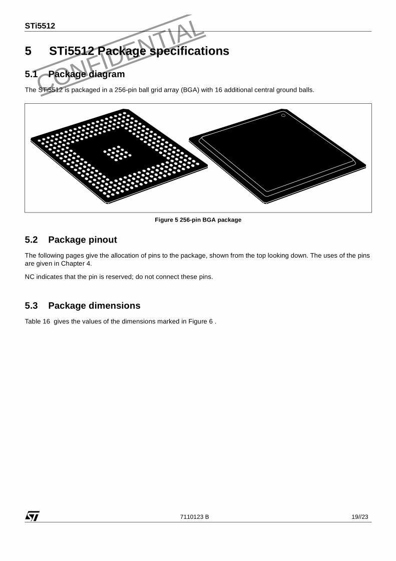
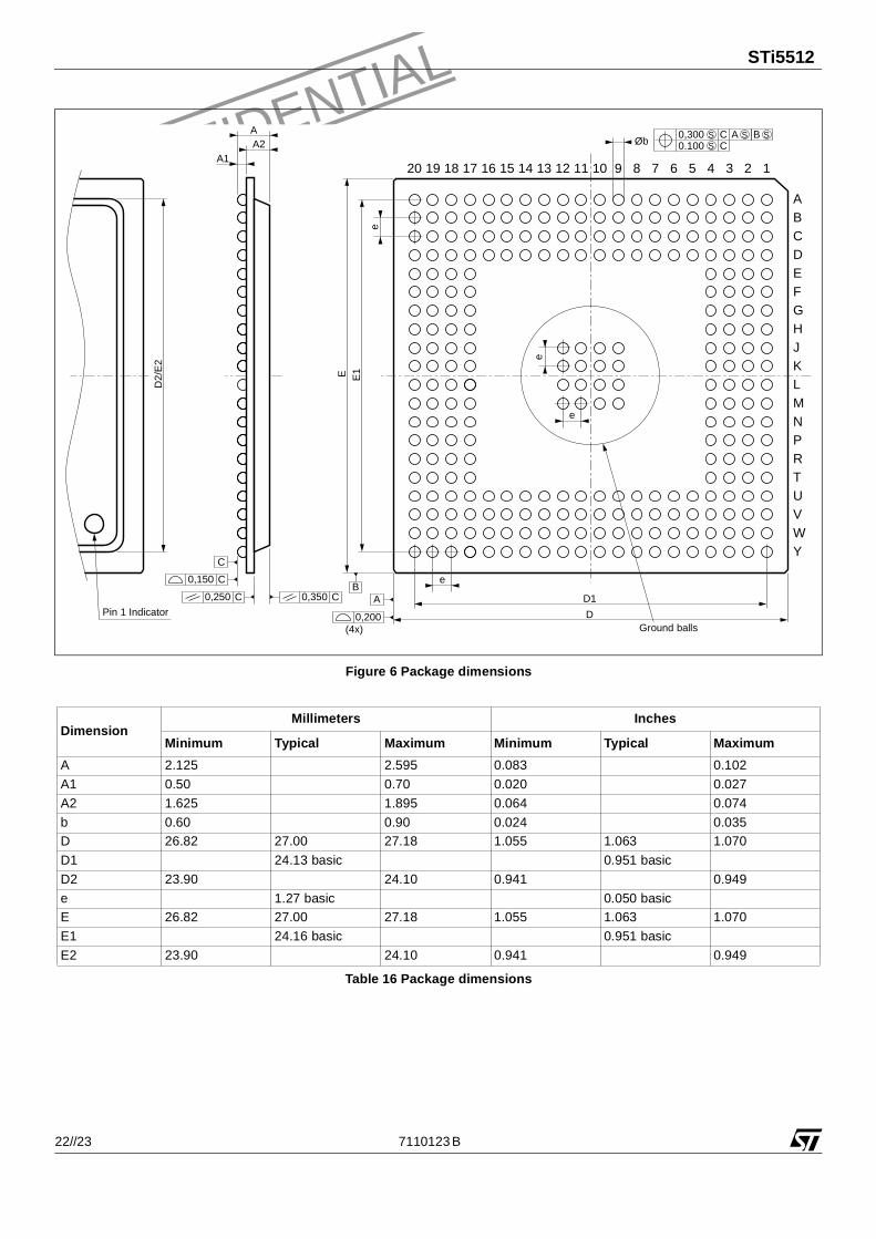
CONFIDENTIA5 STi5512 Package specifications
5.1 Package diagram
The STi5512 is packaged in a 256-pin ball grid array (BGA) with 16 additional central ground balls.
Figure 5 256-pin BGA package
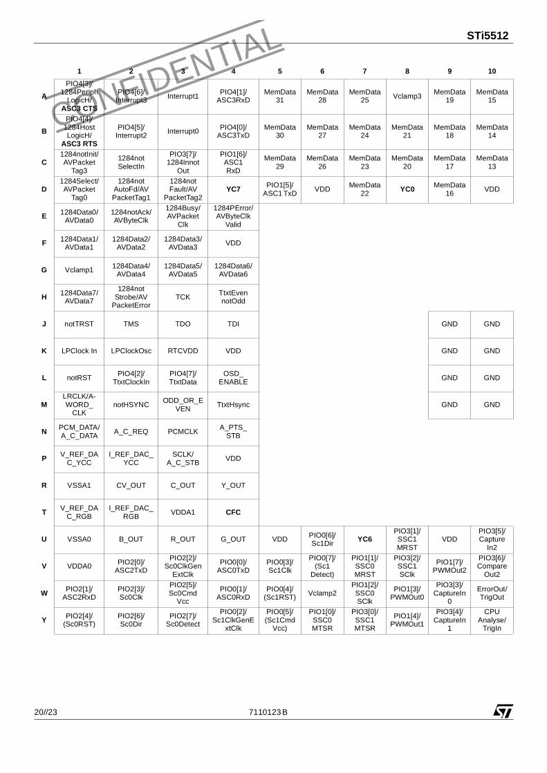
5.2 Package pinout
The following pages give the allocation of pins to the package, shown from the top looking down. The uses of the pins are given in Chapter 4.
NC indicates that the pin is reserved; do not connect these pins.
5.3 Package dimensions
Table 16 gives the values of the dimensions marked in Figure 6 .
7110123 B 19//23
L STi5512
CONFIDENTIA1 2 3 4 5 6 7 8 9 10
A
PIO4[3]/1284Periph
LogicH/ ASC3 CTS
PIO4[6]/Interrupt3 Interrupt1 PIO4[1]/
ASC3RxDMemData
31MemData
28MemData
25 Vclamp3 MemData19
MemData15
B
PIO4[4]/1284Host LogicH/
ASC3 RTS
PIO4[5]/Interrupt2 Interrupt0 PIO4[0]/
ASC3TxDMemData
30MemData
27MemData
24MemData
21MemData
18MemData
14
C1284notInit/AVPacket
Tag3
1284not SelectIn
PIO3[7]/1284Innot
Out
PIO1[6]/ASC1RxD
MemData29
MemData26
MemData23
MemData20
MemData17
MemData13
D1284Select/AVPacket
Tag0
1284not AutoFd/AV PacketTag1
1284not Fault/AV
PacketTag2YC7 PIO1[5]/
ASC1 TxD VDD MemData22 YC0 MemData
16 VDD
E 1284Data0/AVData0
1284notAck/AVByteClk
1284Busy/ AVPacket
Clk
1284PError/AVByteClk
Valid
F 1284Data1/AVData1
1284Data2/AVData2
1284Data3/AVData3 VDD
G Vclamp1 1284Data4/AVData4
1284Data5/AVData5
1284Data6/AVData6
H 1284Data7/AVData7
1284not Strobe/AV
PacketErrorTCK TtxtEven
notOdd
J notTRST TMS TDO TDI GND GND
K LPClock In LPClockOsc RTCVDD VDD GND GND
L notRST PIO4[2]/TtxtClockIn
PIO4[7]/TtxtData
OSD_ ENABLE GND GND
MLRCLK/A-WORD_
CLKnotHSYNC ODD_OR_E
VEN TtxtHsync GND GND
N PCM_DATA/A_C_DATA A_C_REQ PCMCLK A_PTS_
STB
P V_REF_DAC_YCC
I_REF_DAC_YCC
SCLK/A_C_STB VDD
R VSSA1 CV_OUT C_OUT Y_OUT
T V_REF_DAC_RGB
I_REF_DAC_RGB VDDA1 CFC
U VSSA0 B_OUT R_OUT G_OUT VDD PIO0[6]/Sc1Dir YC6
PIO3[1]/SSC1 MRST
VDDPIO3[5]/Capture
In2
V VDDA0 PIO2[0]/ASC2TxD
PIO2[2]/Sc0ClkGen
ExtClk
PIO0[0]/ASC0TxD
PIO0[3]/Sc1Clk
PIO0[7]/(Sc1
Detect)
PIO1[1]/SSC0 MRST
PIO3[2]/SSC1 SClk
PIO1[7]/PWMOut2
PIO3[6]/Compare
Out2
W PIO2[1]/ASC2RxD
PIO2[3]/Sc0Clk
PIO2[5]/Sc0Cmd
Vcc
PIO0[1]/ASC0RxD
PIO0[4]/(Sc1RST) Vclamp2
PIO1[2]/SSC0 SClk
PIO1[3]/PWMOut0
PIO3[3]/CaptureIn
0
ErrorOut/TrigOut
Y PIO2[4]/(Sc0RST)
PIO2[6]/Sc0Dir
PIO2[7]/Sc0Detect
PIO0[2]/Sc1ClkGenE
xtClk
PIO0[5]/(Sc1Cmd
Vcc)
PIO1[0]/SSC0 MTSR
PIO3[0]/SSC1 MTSR
PIO1[4]/PWMOut1
PIO3[4]/CaptureIn
1
CPU Analyse/
TrigIn
20//23 7110123 B

LSTi5512
CONFIDENTIA11 12 13 14 15 16 17 18 19 20
MemData 12 MemData8 MemData5 MemData1 MemAddr
22MemAddr
18MemAddr
15MemAddr
11 MemAddr8 MemAddr7 A
MemData 11 MemData7 MemData4 MemData0 MemAddr
21MemAddr
17MemAddr
14MemAddr
10 MemAddr9 MemAddr6 B
MemData 10 MemData6 MemData3 MemAddr
23MemAddr
20MemAddr
16MemAddr
13 MemAddr3 MemAddr4 MemAddr5 C
MemData9 YC1 MemData2 VDD MemAddr 19 YC2 MemAddr
12notMem CAS2
notMem CAS3 MemAddr2 D
VDD notMem RAS3
notMem CAS0
notMem CAS1 E
notMem RAS2
notMem CSROM
notMem RAS0
notMem RAS1 F
notSDRAM
CS0
notMem BE2
notMem BE3
Mem RdnotWr G
Proc Clockout
notMem CS2
notMem BE0
notMem BE1 H
GND GND VDD MemWait Boot Source0
Boot Source1 J
GND GND Speed Select1 MemGrant MemReq notMem
OE K
GND GND YC3 TSInError TSInByte Clk
Speed Select0 L
GND GND TSInData6 TSInData7 TSIn PacketClk
TSInByte ClkValid M
VDD TSInData3 TSInData4 TSInData5 N
vss_vpll TSInData0 TSInData1 TSInData2 P
YC4 DQ15 aux_clk_ out vdd_vpll R
DQ11 DQ12 DQ13 DQ14 T
YC5 ClockIn VDD AD6 AD12 MEMCLK OUT VDD DQ8 DQ9 DQ10 U
CPUReset AD0 AD3 AD7 AD10 notSDWE notSDCS0 DQ0 DQ6 DQ7 V
LinkOut AD1 AD4 AD8 AD11 not SDCAS notSDCS1/AD13 DQ1 DQ3 DQ5 W
LinkIn AD2 AD5 AD9 MEMCLK IN not SDRAS DQMU DQML DQ2 DQ4 Y
7110123 B 21//23
L STi5512
CONFIDENTIA
Figure 6 Package dimensions
DimensionMillimeters Inches
Minimum Typical Maximum Minimum Typical Maximum
A 2.125 2.595 0.083 0.102
A1 0.50 0.70 0.020 0.027
A2 1.625 1.895 0.064 0.074
b 0.60 0.90 0.024 0.035D 26.82 27.00 27.18 1.055 1.063 1.070
D1 24.13 basic 0.951 basic
D2 23.90 24.10 0.941 0.949
e 1.27 basic 0.050 basicE 26.82 27.00 27.18 1.055 1.063 1.070
E1 24.16 basic 0.951 basic
E2 23.90 24.10 0.941 0.949
Table 16 Package dimensions
1
A
YWVUTRPNMLKJHGFEDCB
20 19 18 17 16 15 14 13 12 11 10 9 8 7 6 5 4 23A1
A2A
D1
D
Optionnal 16 Thermal Balls
Pin 1 Indicator 0,200
A
(4x)
C
CB
0,150
C0,250 C0,350
e
Øb
e
e
E1E
e
D2/
E2
0,300 S0.100
CC
A S B SS
Ground balls
22//23 7110123 B

CONFIDENTIALSTi5512
7110123 B 23/23
AC-3 is a trademark of Dolby Laboratories. Supply of this Implementation of Dolby Technology does not convey a license nor imply a right underany patent, or any other Industrial or Intellectual or Intellectual Property Right of Dolby Laboratories, to use this Implementation in any finished end-user or ready-to-use final product. Companies planning to use this Implementation in products must obtain a license from Dolby Laboratories LicensingCorporation before designing such products.
Information furnished is believed to be accurate and reliable. However, STMicroelectronics assumes no responsibility for the consequences of use ofsuch information nor for any infringement of patents or other rights of third parties which may result from its use. No license is granted by implicationor otherwise under any patent or patent rights of STMicroelectronics. Specifications mentioned in this publication are subject to change without notice.This publication supersedes and replaces all information previously supplied. STMicroelectronics products are not authorized for use as criticalcomponents in life support devices or systems without express written approval of STMicroelectronics.
© 1999 STMicroelectronics - All Rights Reserved
Purchase of I2C components from ST Microelectronics conveys a licence under the Philips I2C patent. Rights to use these components in a I2C system are granted provided that the system conforms to the I2C Standard Specifications as defined by Philips.
is a registered trademark of STMicroelectronics.
STMicroelectronics Website: http://www.st.com
STMicroelectronics GROUP OF COMPANIESAustralia - Brazil - Canada - China - France - Germany - Hong Kong - Italy - Japan - Korea - Malaysia - Malta - Mexico - Morocco -
The Netherlands - Singapore - Spain - Sweden - Switzerland - Taiwan - Thailand - United Kingdom - U.S.A.