c 2011 national technology and science...
TRANSCRIPT


2
c©2011 National Technology and Science Press.
All rights reserved. Neither this book, nor any portion of it, may be copiedor reproduced in any form or by any means without written permission ofthe publisher.

Contents
1 Introduction 71.1 Resources . . . . . . . . . . . . . . . . . . . . . . . . . . . . . . 81.2 Goals for Student Deliverables . . . . . . . . . . . . . . . . . 81.3 Student Deliverables Checklist . . . . . . . . . . . . . . . . . 111.4 Acknowledgements . . . . . . . . . . . . . . . . . . . . . . . . 12
2 Resistive Circuits 132.1 Kirchhoff’s Laws (2-3) . . . . . . . . . . . . . . . . . . . . . . 132.2 Equivalent Resistance (2-4) . . . . . . . . . . . . . . . . . . . . 162.3 Current and Voltage Dividers (2-4) . . . . . . . . . . . . . . . 192.4 Wye-Delta Transformation (2-5) . . . . . . . . . . . . . . . . . 21
3 Analysis Techniques 253.1 Node-Voltage Method (3-1) . . . . . . . . . . . . . . . . . . . 253.2 Mesh-Current Method (3-2) . . . . . . . . . . . . . . . . . . . 293.3 Superposition (3-4) . . . . . . . . . . . . . . . . . . . . . . . . 323.4 Thevenin Equivalents, Maximum Power Transfer (3-5, 3-6) . 35
4 Operational Amplifiers 414.1 Ideal Op-Amp Model (4-3) . . . . . . . . . . . . . . . . . . . . 414.2 Noninverting Amplifier (4-3) . . . . . . . . . . . . . . . . . . 444.3 Summing Amplifier (4-5) . . . . . . . . . . . . . . . . . . . . . 494.4 Signal Processing Circuits (4-8) . . . . . . . . . . . . . . . . . 53
5 RC and RL First-Order Circuits 575.1 Capacitors (5-2) . . . . . . . . . . . . . . . . . . . . . . . . . . 575.2 Inductors (5-3) . . . . . . . . . . . . . . . . . . . . . . . . . . . 625.3 Response of the RC Circuit (5-4) . . . . . . . . . . . . . . . . . 665.4 Response of the RL Circuit (5-5) . . . . . . . . . . . . . . . . . 70

4 CONTENTS
6 RLC Circuits 756.1 Initial and Final Conditions (6-1) . . . . . . . . . . . . . . . . 756.2 Natural Response of the Series RLC Circuit (6-3) . . . . . . . 796.3 General Solution for Any Second-Order Circuit (6-6) . . . . . 846.4 Two-Capacitor Second-Order Circuit (6-6) . . . . . . . . . . . 87
7 AC Analysis 917.1 Impedance Transformations (7-5) . . . . . . . . . . . . . . . . 917.2 Equivalent Circuits (7-6) . . . . . . . . . . . . . . . . . . . . . 977.3 Phase-Shift Circuits (7-8) . . . . . . . . . . . . . . . . . . . . . 1007.4 Phasor-Domain Analysis Techniques (7-9) . . . . . . . . . . . 102
8 AC Power 1058.1 Periodic Waveforms (8-1) . . . . . . . . . . . . . . . . . . . . . 1058.2 Average Power (8-2) . . . . . . . . . . . . . . . . . . . . . . . 1118.3 Complex Power (8-3) . . . . . . . . . . . . . . . . . . . . . . . 1148.4 The Power Factor (8-4) . . . . . . . . . . . . . . . . . . . . . . 117
9 Frequency Response of Circuits and Filters 1219.1 Scaling (9-2) . . . . . . . . . . . . . . . . . . . . . . . . . . . . 1219.2 Bode Plots (9-3) . . . . . . . . . . . . . . . . . . . . . . . . . . 1249.3 Filter Order (9-5) . . . . . . . . . . . . . . . . . . . . . . . . . 1279.4 Cascaded Active Filters (9-7) . . . . . . . . . . . . . . . . . . . 130
10 Laplace Transform Analysis Techniques 13310.1 s-Domain Circuit Analysis (10-7) . . . . . . . . . . . . . . . . 13310.2 Step Response (10-8) . . . . . . . . . . . . . . . . . . . . . . . 13710.3 Transfer Function and Impulse Response (10-8) . . . . . . . . 14010.4 Convolution Integral (10-9) . . . . . . . . . . . . . . . . . . . 143
11 Fourier Analysis Techniques 14711.1 Fourier Series Representation (11-2) . . . . . . . . . . . . . . 14711.2 Circuit Applications (11-3) . . . . . . . . . . . . . . . . . . . . 15211.3 Fourier Transform (11-5) . . . . . . . . . . . . . . . . . . . . . 15411.4 Circuit Analysis with Fourier Transform (11-8) . . . . . . . . 157
A Parts List 159
B LM317 Voltage and Current Sources 163B.1 Variable Voltage Source . . . . . . . . . . . . . . . . . . . . . . 164B.2 Current Source . . . . . . . . . . . . . . . . . . . . . . . . . . . 164

CONTENTS 5
C TL072 Operational Amplifier 169
D DG413 Quad Analog Switch 173
E Transient Response Measurement Techniques 177E.1 Time Constant . . . . . . . . . . . . . . . . . . . . . . . . . . . 177
F Sinusoid Measurement Techniques 179F.1 Amplitude and Phase Measurements . . . . . . . . . . . . . . 179
G Video Links 183

6 CONTENTS

Chapter 1
Introduction
This supplement to Circuits by Ulaby and Maharbiz contains 40 additionalend-of-chapter problems designed for three-way solution: analytical, sim-ulation, and measurement. After solving the problem analytically the stu-dent continues by solving the same problem with NI Multisim and thenonce again with NI myDAQ computer-based instrumentation and circuitcomponents. By iterating on each dimension of the problem until all threeagree students “triangulate on the truth” and develop confidence in theiranalytical and laboratory skills.
Each problem requests at least one common numerical value for com-parison among the three methods. The percent difference between sim-ulated and analytical results as well as measured-to-analytical results in-dicates the degree to which the student has achieved a correct solution.Normally simulation and analytical results agree to within a percentagepoint, and measurements often agree with analytical results to within fivepercent.
The problems are organized as four per chapter for Chapters 2 through11 of Circuits. The table of contents indicates the associated section numberof the textbook in parentheses. Each problem contains the problem state-ment and sufficient detail to guide the student through the simulation andphysical measurement steps. Short video tutorials are linked to each prob-lem to provide detailed guidance on Multisim techniques and ELVISmxcomputer-based instruments for the myDAQ.
This document is fully hyperlinked for section and figure references,and all video links are live hyperlinks. Opening the PDF version of thisdocument is the most efficient way to access all links, and clicking a videohyperlink automatically launches the video in a browser. Within the PDF,

8 CHAPTER 1. INTRODUCTION
use ALT+leftarrow to navigate back to a starting point.
1.1 Resources
• Appendix A details the parts list required to implement all of the cir-cuits and includes links to component distributors.
• Appendix B describes how to implement a variable voltage sourceand two styles of current sources with the LM317 adjustable voltageregulator. Many of the circuits require a DC voltage other than thestandard ±15V and 5V power supplies offered by the NI myDAQ.The adjustable voltage source pictured in Figure B.3 on page 165 shouldbe constructed at the beginning of the term and left in place for sub-sequent circuits.
• Appendix C describes the Texas Instruments TL072 dual operationalamplifier used in many of the circuits. The op amp is frequently usedas a voltage follower to strengthen the 2 mA current drive of the my-DAQ analog outputs. Appendix D describes the Intersil DG413 quadanalog switch used in many of the transient response problems.
• Appendix E details a laboratory technique to measure time constantswhile Appendix F explains how to measure amplitude and phaseshift for sinusoidal signals.
• Appendix G lists all of the available video links.
1.2 Goals for Student Deliverables
Students should document their work in sufficient detail so that it couldbe replicated by others. Present your work on the “Analysis” section asyou would on a standard problem set. Be sure to include a “Given” sectionwith your own drawing of the circuit diagram, a “Find” section that liststhe requested results for the problem, a detailed solution process, and aclearly-identified end result. Do all of this work on engineering green paperor in a lab book or as otherwise required by your instructor.
The “Simulation” section presents your work to set up the circuit simu-lation in NI Multisim and the simulation results you used to obtain mean-ingful information. Create a word processing document that contains anorganized set of screenshots with highlights and annotations as well as text

1.2. GOALS FOR STUDENT DELIVERABLES 9
to lead the reader through the screenshots. Include the circuit schematicand dialog box setup parameters for information not already visible on theschematic – circle parameters that you entered or changed away from de-fault values. Also include simulation results, again circling control settingsthat you changed and highlighting regions where you obtained informa-tion. Figure 1.1 illustrates a screenshot from NI Multisim properly high-lighted to indicate control settings that were adjusted away from defaultvalues as well as regions on the screen where measurements were obtained.Interpret the simulation results by writing them in standard form includingunits, and write any additional calculations that were necessary to reach anend result for simulation.
Figure 1.1: NI Multisim screenshot showing proper markings to indicatecontrol settings adjusted away from default values as well as regions wheremeasurement was obtained.
NOTE: Screen shots in Microsoft Word 2010 can be easily captured andhighlighted as follows:

10 CHAPTER 1. INTRODUCTION
1. Select “Insert” tab and then “Screenshot,”
2. Choose the desired window or select “Screen Clipping” to define anarbitrary region,
3. Select “Shapes,” and
4. Place circles or boxes to highlight important values.
The “Measurement” section presents your work to set up the physicalcircuit and NI ELVISmx signal generators and measurement instruments.This section also includes your measurement results. Follow the generalguidelines for the “Simulation” section. Your instructor may require aphoto of your breadboard circuit and myDAQ connections along with yourstudent ID when you work on the problem outside of scheduled class time.Also include a schematic diagram showing all myDAQ connections.
Finally, the “Summary” section compares the requested numerical re-sults from each of the three methods. Tabulate three results for each re-quested numerical quantity (analytical, simulation, and measurement) andtabulate two percentage differences for each requested numerical quantity:
• Simulation-to-Analytical: [(XS −XA)/XA]× 100%
• Measurement-to-Analytical: [(XM −XA)/XA]× 100%

1.3. STUDENT DELIVERABLES CHECKLIST 11
1.3 Student Deliverables Checklist
1. Engineering paper or lab book – submit directly to instructor:
(a) Analysis
i. “Given / Find” section including original circuitii. Detailed solution
iii. End result clearly identified
(b) Simulation – interpreted results from simulation screen shots
(c) Measurement
i. Circuit schematic with myDAQ connectionsii. Interpreted results
(d) Results comparison table
2. Word processor document – submit electronically to instructor:
(a) Simulation screen shots
i. Circuit schematicii. Dialog box parameters with circles around entered or mod-
ified control valuesiii. Simulation results marked up to highlight key results
(b) Photo of circuit on breadboard and myDAQ connections (if re-quired)
(c) Measurement screen shots
i. ELVISmx signal generator instruments with circles aroundentered or modified values
ii. ELVISmx measurement instruments marked up to highlightkey results and circles around entered or modified controlvalues

12 CHAPTER 1. INTRODUCTION
1.4 Acknowledgements
I gratefully acknowledge contributions from the following individuals:
• Tom Robbins (NTS Press) for his editorial support throughout thisproject,
• Erik Luther (National Instruments) for his enthusiastic support of theNI myDAQ product for engineering education,
• David Salvia (Penn State University) for his helpful suggestions re-garding the design of this project, and
• Rose-Hulman students in Electrical Systems ES203 (Spring 2011) whooffered much helpful feedback on their experience with selected prob-lems.
Ed DoeringDepartment of Electrical and Computer EngineeringRose-Hulman Institute of TechnologyTerre Haute, IN 47803

Chapter 2
Resistive Circuits
2.1 Kirchhoff’s Laws (2-3)
Determine currents I1 to I3 and the voltage V1 in the circuit of Figure 2.1with component values ISRC = 1.8 mA, VSRC = 9.0 V, R1 = 2.2 kΩ, R2 =3.3 kΩ, and R3 = 1.0 kΩ.
Figure 2.1: Circuit for Problem 2.1

14 CHAPTER 2. RESISTIVE CIRCUITS
NI Multisim Measurements
Enter the circuit of Figure 2.1 on the preceding page into NI Multisim andmeasure the currents I1 to I3 and the voltage V1.
• Place components from the “Virtual Components” palette
• Place a Simulate→ Instruments→ Measurement Probe for each cur-rent
• Place a Simulate→ Instruments→ Multimeter to measure the voltageV1
• Use interactive simulation Simulate→ Run
NI Multisim video tutorials:
• Find commonly-used circuit components:http://youtu.be/G6ZJ8C0ja9Q
• Measure DC current with a measurement probe:http://youtu.be/uZ56byigymI
• Measure DC voltage with a voltmeter:http://youtu.be/XLyslyikUws
NI myDAQ Measurements
Build the circuit of Figure 2.1 on the previous page. Use the myDAQ DMM(digital multimeter) to measure the currents I1 to I3 and the voltage V1.
• Implement the voltage source VSRC according to the circuit diagramof Figure B.2 on page 164.
• Measure VSRC with the myDAQ DMM voltmeter and adjust the po-tentiometer to set the voltage as close to 9.0 volts as possible.
• Implement the current source ISRC according to the circuit diagramof Figure B.4 on page 166. Use a 680 Ω resistor for the adjustmentresistor R.
• Measure ISRC with the myDAQ DMM ammeter and confirm that thecurrent is close to 1.8 mA. If you desire more precision, use a 1.0 kΩpotentiometer for R3 and adjust it accordingly.

2.1. KIRCHHOFF’S LAWS (2-3) 15
NI myDAQ video tutorials:
• DMM voltmeter:http://decibel.ni.com/content/docs/DOC-12937
• DMM ammeter:http://decibel.ni.com/content/docs/DOC-12939
Further Exploration with NI myDAQ
Resistor R3 shares the same current as the current source. Study the effectof this resistor on the rest of the circuit.
1. Replace R3 with a 1.0 kΩ potentiometer.
2. Measure current I1 and record the range of currents you observe asyou adjust the potentiometer over its full range.
3. Repeat for currents I2 and I3 and voltage V1.
4. Which of the four measured values appears to be independent of thevalue of R3?
5. Which of the four measured values appears to depend on the valueof R3?
6. Propose an explanation for your observations.

16 CHAPTER 2. RESISTIVE CIRCUITS
2.2 Equivalent Resistance (2-4)
Find the equivalent resistance between the following terminal pairs underthe stated conditions:
1. A-B with the other terminals unconnected,
2. A-D with the other terminals unconnected,
3. B-C with a wire connecting terminals A and D, and
4. A-D with a wire connecting terminals B and C.
Figure 2.2: Circuit for Problem 2.2
Use these component values:
• R1 = 10 kΩ
• R2 = 33 kΩ
• R3 = 15 kΩ
• R4 = 47 kΩ
• R5 = 22 kΩ

2.2. EQUIVALENT RESISTANCE (2-4) 17
NI Multisim Measurements
Enter the circuit of Figure 2.2 on the facing page into NI Multisim and usethe multimeter to measure each of the four resistances under the statedconditions.
• Place components from the “Virtual Components” palette.
• Place a Simulate → Instruments → Multimeter and choose the ohm-meter setting (“Ω” button).
• Place a ground symbol and attach it to one of the multimeter termi-nals.
NI Multisim video tutorials:
• Find commonly-used circuit components:http://youtu.be/G6ZJ8C0ja9Q
• Measure resistance with an ohmmeter:http://youtu.be/3G5V0Hxjkbg
NI myDAQ Measurements
Build the circuit of Figure 2.2 on the preceding page. Use the myDAQDMM (digital multimeter) as an ohmmeter to measure each of the fourresistances under the stated conditions.
• Measure and record the resistance of each resistor individually; dothis before you connect the resistors together.
• Place the resistors to match the resistor orientations shown in Fig-ure 2.2 on the facing page.
• The circuit need not connect to the myDAQ analog ground AGNDterminal; only Multisim requires the ground connection.
NI myDAQ video tutorials:
• DMM ohmmeter:http://decibel.ni.com/content/docs/DOC-12938

18 CHAPTER 2. RESISTIVE CIRCUITS
Further Exploration with NI myDAQ
Ohm’s Law states that a resistor creates a proportional relationship be-tween its voltage and current v = iR where the resistance R is the pro-portionality factor. Setting the resistor voltage v to a known value andmeasuring the resulting current with an ammeter provides another wayto measure resistance. Apply this method to measure each of the four re-sistances and compare with your previous results.
1. Apply the NI myDAQ 5-volt source to the terminals A and D. Usethe 5V and DGND (digital ground) terminals, with 5V connected toterminal A and DGND to terminal D.
2. Use the DMM voltmeter to measure the voltage v as it appears at theresistor network, and then record this value. Expect the voltage to beslightly less than 5.0 volts, and also expect that it will vary somewhatfrom one circuit connection to the next.
3. Use the DMM ammeter to measure the current i flowing into terminalA; record this value, too.
4. Calculate the effective resistance R of the resistor network from yourtwo measurements, and then compare this value to your other mea-surements.
5. Repeat for the remaining three resistance measurements.

2.3. CURRENT AND VOLTAGE DIVIDERS (2-4) 19
2.3 Current and Voltage Dividers (2-4)
Apply the concepts of voltage dividers, current dividers, and equivalentresistance to find the currents I1 to I3 and the voltages V1 to V3.
Figure 2.3: Circuit for Problem 2.3
Use these component values:
• VSRC = 12 V
• R1 = 1.0 kΩ, R2 = 10 kΩ, R3 = 1.5 kΩ, R4 = 2.2 kΩ, R5 = 4.7 kΩ, andR6 = 3.3 kΩ
NI Multisim Measurements
Enter the circuit of Figure 2.3 into NI Multisim. Use measurement probesto measure each current; use voltmeter indicators to measure each voltage.
• Place components from the “Virtual Components” palette.
• Place a ground symbol and attach it to the negative terminal of thevoltage source.

20 CHAPTER 2. RESISTIVE CIRCUITS
• Place a Simulate→ Instruments→ Measurement Probe for each cur-rent.
• Place a voltmeter indicator to display each voltage (see video tutorialfor details).
NI Multisim video tutorials:
• Find commonly-used circuit components:http://youtu.be/G6ZJ8C0ja9Q
• Measure DC current with a measurement probe:http://youtu.be/uZ56byigymI
• Measure DC voltage with a voltmeter indicator:http://youtu.be/8h2SAZ9gkBA
NI myDAQ Measurements
Build the circuit of Figure 2.3 on the preceding page. Use the myDAQDMM (digital multimeter) as a voltmeter to measure each of the three volt-ages; use the DMM as an ammeter to measure each of the three currents.
• Measure and record the resistance of each resistor individually; dothis before you connect the resistors together.
• Place the resistors to match the resistor orientations shown in Fig-ure 2.3 on the previous page.
• Implement the voltage source VSRC according to the circuit diagramof Figure B.2 on page 164.
• Measure VSRC with the myDAQ DMM voltmeter and adjust the po-tentiometer to set the voltage as close to 12.0 volts as possible.
NI myDAQ video tutorials:
• DMM ohmmeter:http://decibel.ni.com/content/docs/DOC-12938
• DMM voltmeter:http://decibel.ni.com/content/docs/DOC-12937
• DMM ammeter:http://decibel.ni.com/content/docs/DOC-12939

2.4. WYE-DELTA TRANSFORMATION (2-5) 21
2.4 Wye-Delta Transformation (2-5)
1. Find the currents I1 and I2.
2. Determine the power delivered by each of the two voltage sources.
Figure 2.4: Circuit for Problem 2.4
Use these component values:
• V1 = 15 V and V2 = 15 V
• R1 = 3.3 kΩ, R2 = 1.5 kΩ, R3 = 4.7 kΩ, R4 = 5.6 kΩ, R5 = 1.0 kΩ,and R6 = 2.2 kΩ
NI Multisim Measurements
Enter the circuit of Figure 2.4 into NI Multisim. Use measurement probesto measure each current, and use the wattmeter to measure the power as-sociated with each voltage source.
• Place components from the “Virtual Components” palette.

22 CHAPTER 2. RESISTIVE CIRCUITS
• Place a ground symbol and attach it to the negative terminal of thevoltage source.
• Place a Simulate→ Instruments→ Measurement Probe for each cur-rent.
• Place a Simulate→ Instruments→Wattmeter for each voltage source,taking care to wire the wattmeters according to the passive sign con-vention.
NI Multisim video tutorials:
• Find commonly-used circuit components:http://youtu.be/G6ZJ8C0ja9Q
• Measure DC current with a measurement probe:http://youtu.be/uZ56byigymI
• Measure DC power with a wattmeter:http://youtu.be/-axVClpMpiU
NI myDAQ Measurements
Build the circuit of Figure 2.4 on the preceding page. Use the myDAQDMM (digital multimeter) as an ammeter to measure each of the two cur-rents; use the DMM as a voltmeter to measure each of the two voltagesource values.
• Measure and record the resistance of each resistor individually; dothis before you connect the resistors together.
• Place the resistors to match the resistor orientations shown in Fig-ure 2.4 on the previous page.
• Use the myDAQ -15V power supply connection for the left voltagesource and the +15V power supply connection for the right voltagesource; connect AGND (Analog Ground) to the node identified by theground symbol.
• Measure the actual values of V1 and V2 when connected to the circuit;expect them to be slightly less than 15 volts.
• Remember to insert the DMM ammeter in series between the voltagesource and the resistor.

2.4. WYE-DELTA TRANSFORMATION (2-5) 23
• Determine power as the product of measured voltage and measuredcurrent.
NI myDAQ video tutorials:
• DMM ohmmeter:http://decibel.ni.com/content/docs/DOC-12938
• DMM voltmeter:http://decibel.ni.com/content/docs/DOC-12937
• DMM ammeter:http://decibel.ni.com/content/docs/DOC-12939

24 CHAPTER 2. RESISTIVE CIRCUITS

Chapter 3
Analysis Techniques
3.1 Node-Voltage Method (3-1)
Apply the node-voltage method to determine the node voltages V1 to V4 forthe circuit of Figure 3.1 on the following page. From these results determinewhich resistor dissipates the most power and which resistor dissipates theleast power, and report these two values of power.
Use these component values:
• Isrc1 = 3.79 mA and Isrc2 = 1.84 mA
• Vsrc = 4.00 V
• R1 = 3.3 kΩ, R2 = 2.2 kΩ, R3 = 1.0 kΩ, and R4 = 4.7 kΩ
NI Multisim Measurements
Enter the circuit of Figure 3.1 on the next page into NI Multisim. Use DCoperating point analysis to determine the four node voltages and the powerdissipated by each resistor.
• Display the net names and rename them to match the four node volt-ages V1 to V4; use only the numbers for the net names.
• Set up a Simulate→ Analyses→ DC Operating Point analysis to dis-play the four node voltages and the power associated with each re-sistor.

26 CHAPTER 3. ANALYSIS TECHNIQUES
Figure 3.1: Circuit for Problem 3.1
NI Multisim video tutorials:
• Display and change net names:http://youtu.be/0iZ-ph9pJjE
• Find node voltages with DC Operating Point analysis:http://youtu.be/gXBCqP17AZs
• Find resistor power with DC Operating Point analysis:http://youtu.be/NxXmVDW9spo
NI myDAQ Measurements
Build the circuit of Figure 3.1. Use the myDAQ DMM (digital multimeter)as a voltmeter to measure each of the four node voltages.
• Implement the voltage source VSRC according to the circuit diagramof Figure B.2 on page 164.

3.1. NODE-VOLTAGE METHOD (3-1) 27
• Measure VSRC with the myDAQ DMM voltmeter and adjust the po-tentiometer to set the voltage as close to 4.00 volts as possible. Recordthe actual voltage you measured.
• Implement the current source Isrc1 according to the circuit diagramof Figure B.5 on page 167. Use a 330 Ω resistor for the adjustmentresistor R.
• Measure Isrc1 with the myDAQ DMM ammeter and confirm that thecurrent is close to 3.79 mA. Record the actual current you measured.
• Implement the current source Isrc2 according to the circuit diagramof Figure B.4 on page 166. Use a 680 Ω resistor for the adjustmentresistor R.
• Measure Isrc2 with the myDAQ DMM ammeter and confirm that thecurrent is close to 1.84 mA. Record the actual current you measured.
NI myDAQ video tutorials:
• DMM voltmeter:http://decibel.ni.com/content/docs/DOC-12937
• Measure node voltage:http://decibel.ni.com/content/docs/DOC-12947
• DMM ammeter:http://decibel.ni.com/content/docs/DOC-12939
Further Exploration with NI myDAQ
As you are by now aware, the analytical solution and the simulation resultsalways agree very well, largely because you can enter exact componentvalues into the simulator. However, the physical circuit component valuesdo not match the nominal values exactly: the 5%-tolerance resistors canvary ±5% from the nominal value represented by the color-coded bands,and the “1250/R mA” formula for the LM317-based current source is anapproximation.
Explore what happens when you recalculate the analytical solution us-ing measured component values.

28 CHAPTER 3. ANALYSIS TECHNIQUES
1. Recalculate the four node voltages using the nominal resistor valuesand the measured values for Isrc1, Isrc2, and VSRC. Create a data ta-ble to compare these values with your analytical results in terms ofdifference and relative difference.
2. Measure and record the five resistances R1 to R4.
3. Recalculate the four node voltages using the measured resistor valuesand the measured values for Isrc1, Isrc2, and VSRC. Create a data ta-ble to compare these values with your analytical results in terms ofdifference and relative difference.
4. Summarize your results: What level of agreement did you achievebetween the analytical solution and the physical measurements?

3.2. MESH-CURRENT METHOD (3-2) 29
3.2 Mesh-Current Method (3-2)
Apply the mesh-current method to determine the mesh currents I1 to I4.From these results determine the voltage across the current source V1.
Figure 3.2: Circuit for Problem 3.2
Use these component values:
• ISRC = 12.5 mA
• VSRC = 15 V
• R1 = 5.6 kΩ, R2 = 2.2 kΩ, R3 = 3.3 kΩ, and R4 = 4.7 kΩ
NI Multisim Measurements
Enter the circuit of Figure 3.2 into NI Multisim. Use “Measurement Probes”and interactive simulation to measure the four mesh currents. Use the mul-timeter or a measurement probe to display the voltage across the currentsource.
• Place the measurement probe on wires that carry only a single meshcurrent; remember that many of the resistors carry two mesh currents.

30 CHAPTER 3. ANALYSIS TECHNIQUES
NI Multisim video tutorials:
• Measure DC mesh current with a measurement probe:http://youtu.be/lK0LcTNroXI
• Measure DC node voltage with a measurement probe:http://youtu.be/svNGHA2-uK4
• Measure DC voltage with a voltmeter:http://youtu.be/XLyslyikUws
NI myDAQ Measurements
Build the circuit of Figure 3.2 on the previous page. Use the myDAQ DMM(digital multimeter) as an ammeter to measure each of the four mesh cur-rents; use the DMM voltmeter to measure the voltage across the currentsource.
• Place the resistors to match the resistor orientations shown in Fig-ure 3.2 on the preceding page. Use 1-inch jumper wires to establishthe top connections between the resistors to facilitate measurement ofthe mesh currents.
• Implement the voltage source VSRC with the NI myDAQ -15V powersupply.
• Implement the current source ISRC according to the circuit diagramof Figure B.4 on page 166. Use a 100 Ω resistor for the adjustmentresistor R.
• Measure ISRC with the myDAQ DMM ammeter and confirm that thecurrent is close to 12.5 mA. If you desire more precision, use a 1.0 kΩpotentiometer for the adjustment resistor.
NI myDAQ video tutorials:
• DMM voltmeter:http://decibel.ni.com/content/docs/DOC-12937
• DMM ammeter:http://decibel.ni.com/content/docs/DOC-12939

3.2. MESH-CURRENT METHOD (3-2) 31
Further Exploration with NI myDAQ
Some types of digital-to-analog converters require binary-weighted cur-rents that can be selectively summed together. With a slight modification toyour existing circuit topology you can redesign it to produce mesh currentsthat meet your own specifications such as those required by the digital-to-analog converter.
1. Consider the modified circuit of Figure 3.3. Apply mesh-current anal-ysis to write a set of equations in terms of the indicated currents andresistor values.
2. Choose resistor values that will establish the binary-weighted currentvalues I2 = ISRC/2, I3 = ISRC/4, I4 = ISRC/8, and I5 = ISRC/16,and that will limit the current source voltage V1 to 5 volts or less.
3. Note: The standard parts list of Appendix A on page 159 includesresistors that are close to the calculated values you need.
4. Build the circuit and measure all five mesh currents I1 to I5.
5. Measure the current source voltage V1.
6. Evaluate your results to determine how well the circuit produces thedesired binary-weighted currents.
Figure 3.3: Modified circuit for Problem 3.2 to produce binary-weightedcurrents.

32 CHAPTER 3. ANALYSIS TECHNIQUES
3.3 Superposition (3-4)
1. Apply the superposition method to determine the current IA and thevoltage VB, i.e., find the current IA1 due to the current source I1 actingalone, the current IA2 due to the voltage source V2 acting alone, andthe current IA3 due to the voltage source V3 acting alone, and thenevaluate the sum IA = IA1 + IA3 + IA3. Make use of current dividersand voltage dividers as much as possible.
2. Use the superposition method to determine the voltage VB.
3. Apply the node-voltage method to find IA and VB, and then comparethese results to those of the superposition method.
Figure 3.4: Circuit for Problem 3.3
Use these component values:
• I1 = 1.84 mA
• V2 = 3.0 V and V3 = 4.9 V
• R1 = 1.0 kΩ, R2 = 2.2 kΩ, and R3 = 4.7 kΩ

3.3. SUPERPOSITION (3-4) 33
NI Multisim Measurements
Enter the circuit of Figure 3.4 on the facing page into NI Multisim. Useinteractive analysis and the voltmeter and ammeter indicators.
• Place the AMMETER_V and VOLTMETER_H components to display thecurrent IA and the voltage VB.
• Set the active source to its intended value, and then set all of the othersources to zero. After stopping the simulator, press Ctrl+Z (“undo”)two times to return the sources to their original values.
• Repeat to determine the responses due to each source acting alone.
NI Multisim video tutorials:
• Measure DC voltage with a voltmeter indicator:http://youtu.be/8h2SAZ9gkBA
• Measure DC current with an ammeter indicator:http://youtu.be/8P4oFw6sIzQ
NI myDAQ Measurements
1. Build the circuit of Figure 3.4 on the preceding page. Use the myDAQDMM to measure IA and VB when all sources are active.
2. Measure IA1 to IA3 by activating only one source at a time. Disablethe other sources by disconnecting the current source (replace it byan open circuit) and disconnecting the voltage source and replacingit with a jumper wire (short circuit).
3. Repeat for VB1 to VB3.
4. Add your results together for each source acting alone, and then com-pare this result to your original measurement when all sources wereactive.
Additional helpful tips:
• Implement the voltage source V2 according to the circuit diagram ofFigure B.2 on page 164.

34 CHAPTER 3. ANALYSIS TECHNIQUES
• Measure V2 with the myDAQ DMM voltmeter and adjust the poten-tiometer to set the voltage as close to 3.00 volts as possible. Recordthe actual voltage you measured.
• Implement the voltage source V3 with the NI myDAQ 5V power sup-ply. Connect the myDAQ digital ground DGND terminal to the ana-log ground AGND at your breadboard.
• Measure V3 with the myDAQ DMM voltmeter when the circuit is con-nected. Expect to find this value slightly less than 5.0 volts. Recordthe actual voltage you measured.
• Implement the current source I1 according to the circuit diagram ofFigure B.4. Use a 680 Ω resistor for the adjustment resistor R.
• Measure I1 with the myDAQ DMM ammeter and confirm that thecurrent is close to 1.84 mA. Record the actual current you measured.
NI myDAQ video tutorials:
• DMM voltmeter:http://decibel.ni.com/content/docs/DOC-12937
• DMM ammeter:http://decibel.ni.com/content/docs/DOC-12939

3.4. THEVENIN EQUIVALENTS, MAXIMUM POWER TRANSFER (3-5, 3-6) 35
3.4 Thevenin Equivalents, Maximum Power Transfer (3-5, 3-6)
1. Find the Thevenin equivalent of the circuit of Figure 3.5 at terminals(a,b) as seen by the load resistance RL.
2. Determine the open-circuit voltage VOC that appears at terminals (a,b).
3. Determine the short-circuit current ISC that flows through a wire con-necting terminals (a,b) together.
4. Determine the maximum power PLmax that could be delivered by thiscircuit.
Figure 3.5: Circuit for Problem 3.4
Use these component values:
• VSRC = 10 V
• R1 = 680 Ω, R2 = 3.3 kΩ, R3 = 4.7 kΩ, and R4 = 1.0 kΩ

36 CHAPTER 3. ANALYSIS TECHNIQUES
NI Multisim Measurements
1. Enter the circuit of Figure 3.5 on the preceding page into NI Multisim.Connect a resistor RL as a load between terminals (a, b).
2. Use interactive analysis and measurement probes to determine theopen-circuit voltage.
3. Use interactive analysis and measurement probes to determine theshort-circuit current.
4. Run a parameter sweep to plot the load resistance power as a func-tion of load resistance connected between terminals (a, b). Use a plotcursor to determine the value of maximum power.
These tips provide more detail about the Multisim techniques for thisproblem:
• Place a measurement probe on terminal b to display the load current.
• Place a measurement probe on terminal a referenced to the probe youplaced on terminal b to display the voltage across the load.
• Set the load resistance to a small yet finite value such as 0.1 Ω. Runthe interactive simulator to determine the short-circuit current.
• Set the load resistance to a large yet finite value such as 100 MΩ; enterthis value as 100MEG rather than 100M because ”m” means ”milli”regardless of case. Run the simulator to determine the open-circuitvoltage.
• Set up a Simulate → Analyses → Parameter Sweep to plot P(RL)over the range 1 Ω to 10 kΩ. Choose a linear plot type, select “DC Op-erating Point” for “Analysis to Sweep,” and plot 100 evenly-spacedpoints to create a smooth curve.
• Use the plot cursors to find the maximum value of the load power.Compare this value to the maximum power you calculated analyti-cally.

3.4. THEVENIN EQUIVALENTS, MAXIMUM POWER TRANSFER (3-5, 3-6) 37
NI Multisim video tutorials:
• Measure DC current with a measurement probe:http://youtu.be/uZ56byigymI
• Measure DC voltage with a referenced measurement probe:http://youtu.be/xKEQ3EXEaP8
• Use a Parameter Sweep analysis to plot resistor power as a functionof resistance:http://youtu.be/3k2g9Penuag
• Find the maximum value of trace in Grapher View:http://youtu.be/MzYK60mfh2Y
NI myDAQ Measurements
1. Build the circuit of Figure 3.5 on page 35. Calculate the Theveninequivalent circuit from the measurements taken in the next two parts.
2. Recall that the DMM voltmeter has very high resistance and thus ap-pears as an open circuit. Connect the voltmeter between terminals(a, b) to measure the open-circuit voltage.
3. Also recall that the DMM ammeter has very low resistance and thusappears as a short circuit. Connect the ammeter between terminals(a, b) to measure the short-circuit current.
4. Connect the variable load circuit shown in Figure 3.6 on the followingpage between terminals (a, b) and connect the myDAQ analog inputchannels to measure the overall load voltage and the voltage that ap-pears across the shunt resistor; this latter voltage is proportional tothe load current. Run the LabVIEW VI “VIPR.vi” (described below)to display the load’s voltage, current, power, and resistance. Firstsweep the potentiometer throughout its full range to get a sense ofthe overall behavior, and then collect and tabulate at least 10 mea-surements of load power and load resistance; adjust the potentiome-ter to take measurements in 1 mW steps. Also record the maximumpower and associated load resistance. Finally, plot the load power asa function of load resistance.
LabVIEW “VIPR.vi” details:

38 CHAPTER 3. ANALYSIS TECHNIQUES
Figure 3.6: Variable load with potentiometer (variable resistor) Rvar andshunt resistor Rsh. The total load resistance is Rvar+Rsh. NI myDAQ Ana-log Input 0 (AI0) monitors the overall load voltage between terminals A-Band Analog Input 1 (AI1) monitors the voltage across the shunt resistor; theload current is the shunt resistor voltage divided by Rsh.
• The LabVIEW VI “VIPR.vi” measures the overall load voltage on ana-log input channel 0 (AI0+ and AI0-) and the shunt resistor voltage onanalog input channel 1 (AI1+ and AI1-). Enter the measured shuntresistance for best accuracy. “VIPR.vi” calculates the load current asthe voltage on AI1 divided by the entered shunt resistance value, theload power as the product of load voltage and current, and the loadresistance as the load voltage divided by the current.
• The measured current value can become somewhat noisy, and “VIPR.vi”applies a noise filter to improve your ability to read the display. Thenoise filter calculates the average value of all of the measurementsaccumulated since the last time the measured voltage changed by at

3.4. THEVENIN EQUIVALENTS, MAXIMUM POWER TRANSFER (3-5, 3-6) 39
least 0.01 volts. Disable the noise filter, if desired.
• “VIPR.vi” is linked at the bottom of http://decibel.ni.com/content/docs/DOC-16389. Download this source file and double-click it to open in LabVIEW; click the “Run” button to start the VI.
NI myDAQ video tutorials:
• DMM voltmeter:http://decibel.ni.com/content/docs/DOC-12937
• DMM ammeter:http://decibel.ni.com/content/docs/DOC-12939
Further Exploration with NI myDAQ
Try this simple yet effective technique to directly measure Thevenin resis-tance:
1. Measure the open-circuit voltage at terminals (a, b),
2. Connect a variable resistor as the load (10 kΩ potentiometer workswell for this circuit),
3. Monitor the load voltage and adjust the potentiometer until the volt-age is exactly one half of the open-circuit voltage,
4. Disconnect the potentiometer from the circuit, and
5. Measure the potentiometer resistance with an ohmmeter; this valueis the Thevenin resistance.
Apply this method to the circuit of this problem and compare your re-sults to your other measurements of Thevenin resistance.
Explain why this method works. HINT: Consider a Thevenin equiv-alent circuit connected to a load resistor and recall what you know aboutvoltage dividers.

40 CHAPTER 3. ANALYSIS TECHNIQUES

Chapter 4
Operational Amplifiers
4.1 Ideal Op-Amp Model (4-3)
1. Determine a general expression for vout in terms of the resistor valuesand iS for the circuit of Figure 4.1 on the next page.
2. Find vout for these specific component values: R1 = 3.3 kΩ, R2 =4.7 kΩ, R3 = 1.0 kΩ, and iS = 1.84 mA.
3. Determine the range of R2 for which −11 ≤ vout ≤ +11 volts.
NI Multisim Measurements
1. Enter the circuit of Figure 4.1 on the following page into NI Multisim.Use the virtual three-terminal op amp model.
2. Measure vout for the given set of component values.
3. Plot vout as a function of R2 with a Simulate → Analyses → Param-eter Sweep analysis of the “DC Operating Point” type. Increase thenumber of points as needed to ensure an adequate number of mea-surements to characterized the op amp output voltage in the regionof the specified voltage limits.

42 CHAPTER 4. OPERATIONAL AMPLIFIERS
Figure 4.1: Circuit for Problem 4.1
NI Multisim video tutorials:
• Use a Parameter Sweep analysis to plot resistor power as a functionof resistance:http://youtu.be/3k2g9Penuag
• Measure DC node voltage with a measurement probe:http://youtu.be/svNGHA2-uK4
NI myDAQ Measurements
1. Build the circuit of Figure 4.1 with the given component values. Im-plement the current source Isrc1 according to the circuit diagram ofFigure B.4 on page 166. Use a 680 Ω resistor for the adjustment resis-torR. When complete, measure and record the source current iS withthe DMM ammeter and confirm that it is close to 1.84 mA.
2. Measure the value of the vout with the DMM voltmeter.

4.1. IDEAL OP-AMP MODEL (4-3) 43
3. Replace R2 with a 10 kΩ potentiometer. Monitor vout and adjust thepotentiometer until the voltage reaches the specified limit. Discon-nect the potentiometer from the circuit and then measure its resis-tance with the DMM ohmmeter.
Additional helpful tips for this section:
• Use the Texas Instruments TL072 op amp described in Appendix C.Follow the pinout diagram of Figure C.1 on page 170 for either of thetwo available op amps in the package. You may also use an equiva-lent dual-supply op amp.
• Power the op amp with myDAQ +15V to VCC+ and -15V to VCC−.Use AGND for the circuit ground.
NI myDAQ video tutorials:
• DMM voltmeter:http://decibel.ni.com/content/docs/DOC-12937
• DMM ammeter:http://decibel.ni.com/content/docs/DOC-12939

44 CHAPTER 4. OPERATIONAL AMPLIFIERS
4.2 Noninverting Amplifier (4-3)
The circuit in Figure 4.2 uses a potentiometer whose total resistance is R1.The movable stylus on terminal 2 creates two variable resistors: βR1 be-tween terminals 1–2 and (1 − β)R1 between terminals 2–3. The movablestylus varies β over the range 0 ≤ β ≤ 1.
1. Obtain an expression for G = vo/vs in terms of β.
2. Calculate the amplifier gain for β = 0.0, β = 0.5, and β = 1.0 withcomponent values R1 = 10 kΩ and R2 = 1.5 kΩ.
3. Let vs be a 100-Hz sinusoidal signal with a 1-volt peak value. Plot voand vs to scale for β = 0.0, β = 0.5, and β = 1.0.
Figure 4.2: Circuit for Problem 4.2
NI Multisim Measurements
1. Enter the circuit of Figure 4.2 into NI Multisim. Use these specificcomponents: OPAMP 3T VIRTUAL, AC VOLTAGE, and virtual linear

4.2. NONINVERTING AMPLIFIER (4-3) 45
potentiometer; see the video tutorial below to learn how to search forparts by name. Set the AC voltage source frequency to 100 Hz.
2. Observe vs and vo with the oscilloscope. Vary the potentiometer valueover its full range of 0 to 100%, and then use the oscilloscope cursorsto measure the circuit gain for β = 0.0, β = 0.5, and β = 1.0.
3. Print screen shots of the oscilloscope for β = 0.0, β = 0.5, and β =1.0. Use the same Channel A and Channel B vertical scale (volts perdivision) for all three screen shots.
Additional helpful tips:
• Use the Simulate → Instruments → Oscilloscope with vs on Chan-nel A and vo on Channel B. Run an interactive simulation until severalcycles of oscillation appear on the oscilloscope display.
• Use the cursors to measure the peak values of the input and outputsignals, and then calculate the amplifier gain as the output value di-vided by the input value.
NI Multisim video tutorials:
• Find components by name:http://youtu.be/5wlFweh4n-c
• AC (sinusoidal) voltage source:http://youtu.be/CXbuz7MVLSs
• Basic operation of the two-channel oscilloscope:http://youtu.be/qnRK6QyqjvQ
• Waveform cursor measurements with the two-channel oscilloscope:http://youtu.be/snBRFq1Y1q4
NI myDAQ Measurements
1. Build the circuit of Figure 4.2 on the facing page with the given com-ponent values. Use the following myDAQ signal connections:
• AO0 (Analog Output 0) for vs,
• AI0 (Analog Input 0) to display vs; connect AI0+ to the sourcevoltage and AI0- to ground, and

46 CHAPTER 4. OPERATIONAL AMPLIFIERS
• AI1 (Analog Input 1) to display vo; connect AI1+ to the outputvoltage and AI1- to ground.
Create the 100-Hz sinusoidal waveform with the NI ELVISmx Func-tion Generator.
2. Observe vs and vo with the NI ELVISmx Oscilloscope. Vary the po-tentiometer value over its full range of 0 to 100%, and then use theoscilloscope cursors to measure the circuit gain for β = 0.0, β = 0.5,and β = 1.0.
3. Print screen shots of the oscilloscope for β = 0.0, β = 0.5, and β =1.0. Use the same Channel 0 and Channel 1 vertical scale (volts perdivision) for all three screen shots.
Additional helpful tips:
• Use the Texas Instruments TL072 op amp described in Appendix C.Follow the pinout diagram of Figure C.1 on page 170 for either of thetwo available op amps in the package. You may also use an equiva-lent dual-supply op amp.
• Power the op amp with myDAQ +15V to VCC+ and -15V to VCC−.Use AGND for the circuit ground.
• The potentiometer terminals of Figure 4.2 on page 44 follow the stan-dard pinout used by single-turn trim potentiometers. If your poten-tiometer does not label the pins, the stylus pin (Pin 2) is normallyplaced between Pins 1 and 3.
NI myDAQ video tutorials:
• Oscilloscope:http://decibel.ni.com/content/docs/DOC-12942
• Function Generator (FGEN):http://decibel.ni.com/content/docs/DOC-12940
Further Exploration with NI myDAQ
Signal amplifiers apply a gain G ≥ 1 to increase the amplitude of weaksignals, thereby making the signal information easier to use elsewhere inthe system. Use a voltage divider circuit (known as an attenuator in this
4.2. NONINVERTING AMPLIFIER (4-3) 47
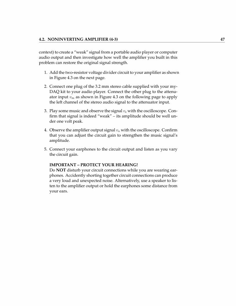
context) to create a “weak” signal from a portable audio player or computeraudio output and then investigate how well the amplifier you built in thisproblem can restore the original signal strength.
1. Add the two-resistor voltage divider circuit to your amplifier as shownin Figure 4.3 on the next page.
2. Connect one plug of the 3.2 mm stereo cable supplied with your my-DAQ kit to your audio player. Connect the other plug to the attenu-ator input vm as shown in Figure 4.3 on the following page to applythe left channel of the stereo audio signal to the attenuator input.
3. Play some music and observe the signal vs with the oscilloscope. Con-firm that signal is indeed “weak” – its amplitude should be well un-der one volt peak.
4. Observe the amplifier output signal vo with the oscilloscope. Confirmthat you can adjust the circuit gain to strengthen the music signal’samplitude.
5. Connect your earphones to the circuit output and listen as you varythe circuit gain.
IMPORTANT – PROTECT YOUR HEARING!Do NOT disturb your circuit connections while you are wearing ear-phones. Accidently shorting together circuit connections can producea very loud and unexpected noise. Alternatively, use a speaker to lis-ten to the amplifier output or hold the earphones some distance fromyour ears.

48 CHAPTER 4. OPERATIONAL AMPLIFIERS
Figure 4.3: Circuit for Problem 4.2 with voltage-divider attenuator and au-dio signal connections. The music signal is vm, the attenuated signal to beamplified is vs, and the amplified signal is vo.
4.3. SUMMING AMPLIFIER (4-5) 49
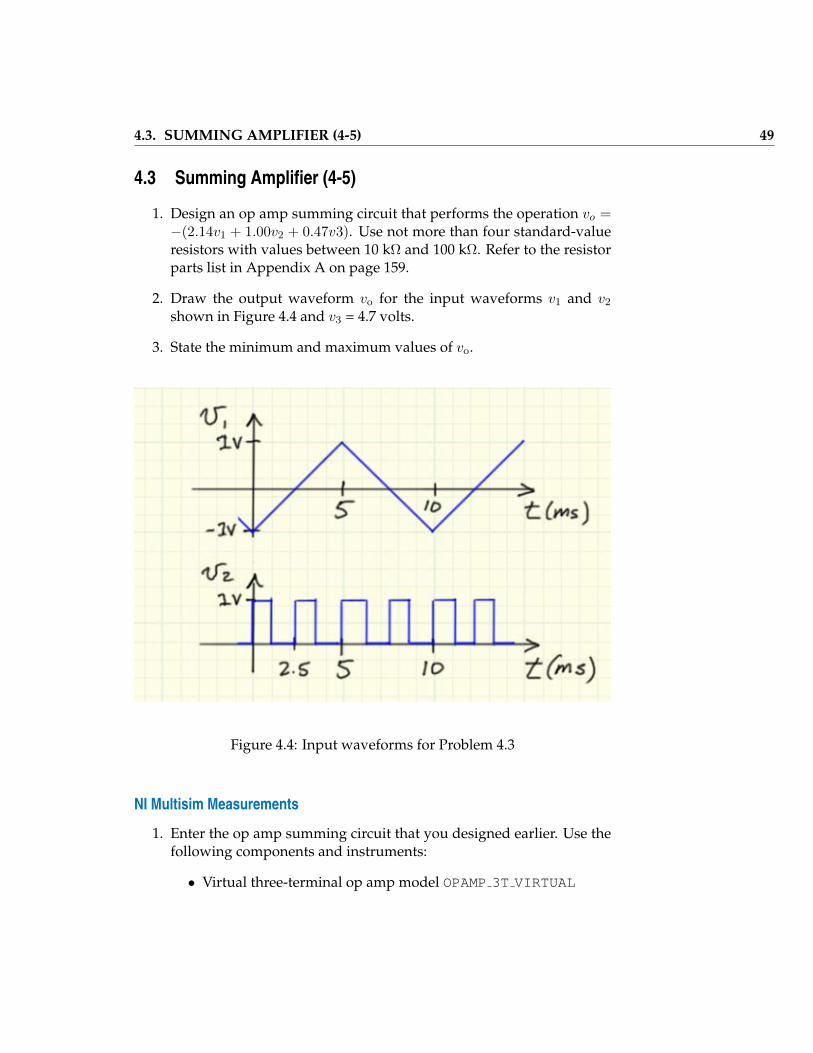
4.3 Summing Amplifier (4-5)
1. Design an op amp summing circuit that performs the operation vo =−(2.14v1 + 1.00v2 + 0.47v3). Use not more than four standard-valueresistors with values between 10 kΩ and 100 kΩ. Refer to the resistorparts list in Appendix A on page 159.
2. Draw the output waveform vo for the input waveforms v1 and v2shown in Figure 4.4 and v3 = 4.7 volts.
3. State the minimum and maximum values of vo.
Figure 4.4: Input waveforms for Problem 4.3
NI Multisim Measurements
1. Enter the op amp summing circuit that you designed earlier. Use thefollowing components and instruments:
• Virtual three-terminal op amp model OPAMP 3T VIRTUAL

50 CHAPTER 4. OPERATIONAL AMPLIFIERS
• Piecewise-linear voltage source PIECEWISE LINEAR VOLTAGEfor v1• Pulse voltage source PULSE VOLTAGE for v2• Four-channel oscilloscope
2. Plot vo and the three inputs v1 to v3 with the four-channel oscillo-scope.
3. Use the oscilloscope display cursors to identify the minimum andmaximum values of vo.
Additional Multisim tips for this problem:
• Specify the PWL voltage source waveform by entering endpoints ofstraight lines as time-voltage pairs. The triangle waveform of Fig-ure 4.4 on the previous page requires only three entries to specify acomplete period. Select “Repeat data during simulation” to create aperiodic triangle waveform.
• Three fields need to be adjusted for the pulse voltage source to makeit match the required square waveform shape: “Initial Value,” “PulseWidth,” and “Period.”
NI Multisim video tutorials:
• Basic operation of the four-channel oscilloscope:http://youtu.be/iUqs_c1Bc4Y
• Piecewise linear (PWL) voltage source:http://youtu.be/YYU5WuyebD0
• Pulse voltage source:http://youtu.be/RdgxVfr28C8
• Find components by name:http://youtu.be/5wlFweh4n-c
NI myDAQ Measurements
1. Build the op amp summing circuit that you designed earlier. Use thefollowing myDAQ signal connections:
• AO0 (Analog Output 0) for v1,

4.3. SUMMING AMPLIFIER (4-5) 51
• AO1 (Analog Output 1) for v2,
• AI0 (Analog Input 0) to display either v1 or v2; connect AI0+ tothe input voltage of interest and AI0- to ground,
• AI1 (Analog Input 1) to display vo; connect AI1+ to the outputvoltage and AI1- to ground,
Create the triangle and square waveforms with the NI ELVISmx Ar-bitrary Waveform Generator; use 50 kS/s as the sampling rate.
IMPORTANT: The two waveform files must of the same length (10 ms).
2. Plot vo and v1 with the NI ELVISmx Oscilloscope. Repeat with v2.
3. Use the oscilloscope display cursors to identify the minimum andmaximum values of vo.
Additional tips for this problem:
• Use the Texas Instruments TL072 op amp described in Appendix Con page 169. Follow the pinout diagram of Figure C.1 on page 170 foreither of the two available op amps in the package. You may also usean equivalent dual-supply op amp.
• Power the op amp with myDAQ +15V to VCC+ and -15V to VCC−.Use AGND for the circuit ground.
• Implement the constant voltage source v3 according to the circuit di-agram of Figure B.2 on page 164. Adjust the potentiometer until themeasured voltage is as close to 4.70 volts as possible.
NI myDAQ video tutorials:
• DMM voltmeter:http://decibel.ni.com/content/docs/DOC-12937
• Arbitrary Waveform Generator (ARB):http://decibel.ni.com/content/docs/DOC-12941
• Oscilloscope:http://decibel.ni.com/content/docs/DOC-12942

52 CHAPTER 4. OPERATIONAL AMPLIFIERS
Further Exploration with NI myDAQ
Investigate the effect of the gain constants for waveform inputs v1 and v2.You can quickly and easily vary a resistor value by placing another resistorin parallel with it, thereby reducing the effective resistance. Place a 10 kΩ inparallel with the source resistor associated with waveform v1 and observethe impact on the output voltage waveform. Plot the new output wave-form, summarize the difference from the original waveform, and explainwhy reducing the resistor value causes this change in appearance.
Repeat the experiment with the source resistor associated with wave-form v2.

4.4. SIGNAL PROCESSING CIRCUITS (4-8) 53
4.4 Signal Processing Circuits (4-8)
1. Design a two-stage signal processor to serve as a “distortion box”for an electric guitar. The first-stage amplifier applies a variable gainmagnitude in the range 13.3 to 23.3 while the second-stage amplifierattenuates the signal by 13.3, i.e., the second-stage amplifier has afixed gain of 1/13.3. Note that when the first-stage amplifier gain is13.3 the overall distortion box gain is unity. The distortion effect relieson intentionally driving the first-stage amplifier into saturation (alsocalled “clipping”) when its gain is higher than 13.3.
Use a 10 kΩ potentiometer and standard-value resistors in the range1.0 kΩ to 100 kΩ; see the resistor parts list in Appendix A on page 159.You may combine two standard-value resistors in series to achievethe required amplifier gains.
2. Derive a general formula for percent clipping of a unit-amplitude si-nusoidal test signal; this is the percent of time during one period inwhich the signal is clipped. The formula includes the peak sinusoidalvoltage VP that would appear at the output of the first-stage ampli-fier with saturation ignored and the actual maximum value VS due tosaturation.
3. Apply your general formula to calculate percent clipping of a 1-voltpeak amplitude sinusoidal signal for the potentiometer dial in threepositions: fully counter-clockwise (no distortion), midscale (moder-ate distortion), and fully clockwise (maximum distortion). Assumethe op amp outputs saturate at ±13.5 volts.
4. Apply a 1-volt peak amplitude sinusoidal signal with 100-Hz fre-quency to the distortion box input and plot its output for the poten-tiometer dial in the same three positions as above. State the maximumand minimum values of the distortion box output.
NI Multisim Measurements
1. Enter your design for the distortion box into NI Multisim. Use the vir-tual five-terminal op amp model for both stages. Connect the powersupply terminals±13.5 volts. Apply the AC (sinusoidal) voltage sourceas the signal input; configure the source for 1-volt peak amplitudeand 100 Hz frequency.

54 CHAPTER 4. OPERATIONAL AMPLIFIERS
2. Observe the distortion box input and output signals with the oscil-loscope and vary the potentiometer value over its full range of 0 to100%, and then use the oscilloscope cursors to measure the percentclipping for the potentiometer settings 0%, 50%, and 100%.
3. Print screenshots of the oscilloscope display to show the distortionbox input and output signals for the three potentiometer settings inthe previous step.
4. Measure the maximum and minimum values of the distortion boxoutput.
Additional helpful tips:
• Use these specific components: OPAMP 5T VIRTUAL, AC VOLTAGE,and virtual linear potentiometer.
• Remember that the five-terminal op amp symbol when initially placedhas its positive power supply connection on top; applying a verticalflip to the symbol also flips the positive power supply connection tothe bottom.
• Place the “CMOS Supply (VDD)” as the op amp positive power sup-ply connection and “CMOS Supply (VSS)” as the negative power sup-ply connection.
• Use the basic two-channel oscilloscope with the distortion box signalinput on Channel A and its output on Channel B. Run an interac-tive simulation until several cycles of oscillation appear on the oscil-loscope display.
• Take cursor measurements to determine the time duration of clippingfor a half-cycle of the sinusoidal signal. Divide this time by the dura-tion of the entire half-cycle and multiply by 100%.

4.4. SIGNAL PROCESSING CIRCUITS (4-8) 55
NI Multisim video tutorials:
• Basic operation of the two-channel oscilloscope:http://youtu.be/qnRK6QyqjvQ
• Waveform cursor measurements with the two-channel oscilloscope:http://youtu.be/snBRFq1Y1q4
• AC (sinusoidal) voltage source:http://youtu.be/CXbuz7MVLSs
• VDD and VSS power supply voltages:http://youtu.be/XrPVLgYsDdY
NI myDAQ Measurements
1. Build your distortion box circuit and use the following myDAQ sig-nal connections:
• AI0 (Analog Input 0) to display the input signal; connect AI0+ tothe source voltage and AI0- to ground,
• AI1 (Analog Input 1) to display the output signal; connect AI1+to the output voltage and AI1- to ground,
Create the 100-Hz sinusoidal waveform with the NI ELVISmx Func-tion Generator.
2. Observe the distortion box input and output signals with the NI ELVISmxOscilloscope and vary the potentiometer over its full range. Use theoscilloscope cursors to measure the percent clipping with the poten-tiometer dial in three positions: fully counter-clockwise (no distor-tion), midscale (moderate distortion), and fully clockwise (maximumdistortion).
3. Print screenshots of the oscilloscope display to show the distortionbox input and output signals for the three potentiometer settings inthe previous step.
4. Measure the maximum and minimum values of the distortion boxoutput.
Additional helpful tips:

56 CHAPTER 4. OPERATIONAL AMPLIFIERS
• Use the Texas Instruments TL072 op amp described in Appendix Con page 169. Follow the pinout diagram of Figure C.1 on page 170 forthe two available op amps in the package. You may also use a pair ofequivalent dual-supply op amp.
• Power the op amp with myDAQ +15V to VCC+ and -15V to VCC−.Use AGND for the circuit ground.
• The TL072 op amp and similar devices saturate at approximately 1.5volts under the supply voltage, consequently the actual saturationlevels are about±13.5 volts. If you use a different type of op amp withrail-to-rail outputs then you should expect to see the output saturationlevels match the measured values of the myDAQ 15-volt dual powersupply.
• Should you need to observe the output of the first-stage amplifierwith the oscilloscope for troubleshooting purposes, you must con-sider the ±10 volt input range limitation of the myDAQ analog inputchannels. This range limit effectively makes you blind to any signalactivity between 10 volts and the myDAQ power supply of 15 volts.
• Take cursor measurements to determine the time duration of clippingfor a half-cycle of the sinusoidal signal. Divide this time by the dura-tion of the entire half-cycle and multiply by 100%.
NI myDAQ video tutorials:
• Oscilloscope:http://decibel.ni.com/content/docs/DOC-12942
• Function Generator (FGEN):http://decibel.ni.com/content/docs/DOC-12940

Chapter 5
RC and RL First-Order Circuits
5.1 Capacitors (5-2)
The voltage v(t) across a 10-µF capacitor is given by the waveform shownin Figure 5.1.
1. Determine the equation for the capacitor current i(t) and plot it overthe time 0 to 50 ms.
2. Calculate the values of capacitor current at times 0, 25, and 30 ms.
Figure 5.1: Voltage waveform for Problem 5.1

58 CHAPTER 5. RC AND RL FIRST-ORDER CIRCUITS
NI Multisim Measurements
Oscilloscopes display a time-varying voltage as a function of time. The cur-rent through a component such as the capacitor in this problem can also bedisplayed on an oscilloscope with a small-valued “shunt resistor” placedin series with the component. The shunt resistor produces a proportionalvoltage according to Ohm’s Law v = Ri where the resistance R serves asthe proportionality constant. A trade-off exists here: a small shunt resis-tance minimizes disruption to the surrounding circuit, but a large shuntresistance maximizes the available signal to the oscilloscope.
1. Enter a circuit that contains the following components:
• 10-µF capacitor and 10-Ω shunt resistor connected in series
• ABM (Analog Behavioral Modeling) voltage source (ABM VOLTAGE)connected across the capacitor-resistor combination; set up thevoltage value to match the waveform of Figure 5.1 on the previ-ous page.
• Two-channel oscilloscope showing the capacitor voltage on Chan-nel A and the shunt resistor voltage on Channel B.
Run interactive simulation, adjusting the oscilloscope settings to dis-play the capacitor voltage and current with each waveform filling areasonable amount of the available display.
2. Use the oscilloscope display cursors to measure the capacitor currentat times 0, 25, and 30 ms. Divide the cursor measurement by the shuntresistor value.
Additional Multisim tips for this problem:
• Build the ABM voltage source “Voltage Value” string by combiningthe following functions:
– u(TIME) – Step function u(t)
– uramp(TIME) – Ramp function r(t)
– exp(TIME) – Exponential function et
For example, the string 800*(uramp(TIME) - uramp(TIME-0.01))implements the first 20 milliseconds of the capacitor voltage wave-form.

5.1. CAPACITORS (5-2) 59
• Place a DC voltage source someplace on the schematic sheet to enableinteractive simulation. Do not connect the DC source to the capacitorcircuit itself.
NI Multisim video tutorials:
• Basic operation of the two-channel oscilloscope:http://youtu.be/qnRK6QyqjvQ
• Waveform cursor measurements with the two-channel oscilloscope:http://youtu.be/snBRFq1Y1q4
• ABM (Analog Behavioral Model) voltage source:http://youtu.be/8pPynWRwhO4
• Distinguish oscilloscope traces by color:http://youtu.be/bICbjggcTiQ
NI myDAQ Measurements
The myDAQ analog outputs AO0 and AO1 cannot source more than 2 mAand still maintain the expected voltage output. Use an op amp voltagefollower (see Ulaby Section 4-7) to create a “strengthened” copy of the my-DAQ analog output.
1. Construct a circuit similar to the Multisim circuit you created earlier,i.e., place a 10-ohm shunt resistor in series with the capacitor, and con-nect the capacitor-resistor combination between the voltage followeroutput and ground.
IMPORTANT: Electrolytic capacitors are polarized; ensure that thepositive-labeled terminal connects to the op amp output. Alterna-tively, if the capacitor is marked with a negative-labeled terminal,connect this terminal to the shunt resistor.
Establish the following myDAQ connections:
• AO0 (Analog Output 0) to the voltage follower input,
• AI0 (Analog Input 0) to display the capacitor voltage; connectAI0+ to the positive capacitor terminal and AI0- to the negativecapacitor terminal,
• AI1 (Analog Input 1) to display the shunt resistor voltage; con-nect AI1- to ground.

60 CHAPTER 5. RC AND RL FIRST-ORDER CIRCUITS
Create the capacitor voltage waveform of Figure 5.1 on page 57 withthe NI ELVISmx Arbitrary Waveform Generator; use 50 kS/s as thesampling rate.
Adjust the NI ELVISmx Oscilloscope settings to display the capacitorvoltage and current with each waveform filling a reasonable amountof the available display. Use a combination of edge triggering onChannel 0 and the “Horizontal Position” control to place the upperleft corner of the voltage waveform at time 10 ms.
2. Use the oscilloscope display cursors to measure the capacitor currentat times 0, 25, and 30 ms. Divide the cursor measurement by theshunt resistor value. Improve your measurement accuracy by usingthe measured shunt resistance obtained by the myDAQ DMM ohm-meter.
Additional tips for this problem:
• Use the Texas Instruments TL072 op amp described in Appendix Con page 169 for the voltage follower. Follow the pinout diagram ofFigure C.1 on page 170 for either of the two available op amps in thepackage. You may also use an equivalent dual-supply op amp.
• Power the op amp with myDAQ +15V to VCC+ and -15V to VCC−.Use AGND for the circuit ground.
• Use Cursor 1 to take measurements on the shunt resistor voltage.Leave Cursor 2 at time zero to make the “dT” indicator show timedirectly.
• The shunt resistor voltage signal is relatively low amplitude. Expectthe waveform to jump vertically somewhat. Simply click the oscillo-scope “Stop” button to freeze the display.
• Create three waveform segments with the ARB “Waveform Editor,”two of length 10 ms and the third of length 30 ms. Choose the “Ex-pression” option for each segment and enter expressions that includethe time variable t as needed. Set the “X Range From” value of the30 ms segment to 0.03 seconds and set “Cycles” to 1. You can then en-ter the exponential function exp() as shown in Figure 5.1 on page 57.For convenience, create the complete waveform with a unit ampli-tude and then adjust the “Gain” value of the Arbitrary WaveformGenerator to 8.

5.1. CAPACITORS (5-2) 61
NI myDAQ video tutorials:
• Arbitrary Waveform Generator (ARB):http://decibel.ni.com/content/docs/DOC-12941
• Oscilloscope:http://decibel.ni.com/content/docs/DOC-12942
• Increase current drive of analog output (AO) channels with anop amp voltage follower:http://decibel.ni.com/content/docs/DOC-12665

62 CHAPTER 5. RC AND RL FIRST-ORDER CIRCUITS
5.2 Inductors (5-3)
The voltage v(t) across a 33-mH inductor is given by the sinusoidal pulsewaveform shown in Figure 5.2.
1. Determine the equation for the inductor current i(t) and plot it overthe time 0 to 0.4 ms. Assume zero initial inductor current.
2. Determine the time at which the inductor current reaches its maxi-mum value.
3. Calculate the total range of inductor current, i.e., the maximum valueminus the minimum value.
Figure 5.2: Voltage waveform for Problem 5.2
NI Multisim Measurements
Oscilloscopes display a time-varying voltage as a function of time. The cur-rent through a component such as the inductor in this problem can also bedisplayed on an oscilloscope with a small-valued “shunt resistor” placed

5.2. INDUCTORS (5-3) 63
in series with the component. The shunt resistor produces a proportionalvoltage according to Ohm’s Law v = Ri where the resistance R serves asthe proportionality constant. A trade-off exists here: a small shunt resis-tance minimizes disruption to the surrounding circuit, but a large shuntresistance maximizes the available signal to the oscilloscope.
1. Enter a circuit that contains the following components:
• 33-mH inductor and 10-Ω shunt resistor connected in series
• Two AC voltage sources (AC VOLTAGE) connected in series andalso connected across the inductor-resistor combination. Flip theorientation of one of the sources so that the series combinationforms the difference of the two voltages. Set one voltage for a de-lay of 0.1 ms and the other for a delay of 0.3 ms; in this way onlya single cycle of the sinusoid appears across the pair of sourcesas in the waveform of Figure 5.2 on the preceding page.
• Two-channel oscilloscope showing the inductor voltage on Chan-nel A and the shunt resistor voltage on Channel B.
Run interactive simulation, adjusting the oscilloscope settings to dis-play the inductor voltage and current with each waveform filling areasonable amount of the available display.
2. Use the oscilloscope display cursors to measure the time at which theinductor current reaches its maximum value.
3. Use the oscilloscope cursors to determine the total range of inductorcurrent, i.e., the maximum value minus the minimum value.
NI Multisim video tutorials:
• Basic operation of the two-channel oscilloscope:http://youtu.be/qnRK6QyqjvQ
• Waveform cursor measurements with the two-channel oscilloscope:http://youtu.be/snBRFq1Y1q4
• AC (sinusoidal) voltage source:http://youtu.be/CXbuz7MVLSs
• Distinguish oscilloscope traces by color:http://youtu.be/bICbjggcTiQ

64 CHAPTER 5. RC AND RL FIRST-ORDER CIRCUITS
NI myDAQ Measurements
The myDAQ analog outputs AO0 and AO1 cannot source more than 2 mAand still maintain the expected voltage output. Use an op amp voltagefollower (see Ulaby Section 4-7) to create a “strengthened” copy of the my-DAQ analog output.
1. Construct a circuit similar to the Multisim circuit you created earlier,i.e., place a 10-ohm shunt resistor in series with the inductor, and con-nect the inductor-resistor combination between the voltage followeroutput and ground.
Establish the following myDAQ connections:
• AO0 (Analog Output 0) to the voltage follower input,
• AI0 (Analog Input 0) to display the inductor voltage; connectAI0+ to inductor terminal connected to the op amp output andconnect AI0- to the other inductor terminal,
• AI1 (Analog Input 1) to display the shunt resistor voltage; con-nect AI1- to ground.
Create the inductor voltage waveform of Figure 5.2 on page 62 withthe NI ELVISmx Arbitrary Waveform Generator; use 200 kS/s as thesampling rate.
Adjust the NI ELVISmx Oscilloscope settings to display the inductorvoltage and current with each waveform filling a reasonable amountof the available display. Use a combination of edge triggering onChannel 0 and the “Horizontal Position” control to center the induc-tor voltage pulse.
2. Use the oscilloscope display cursors to measure the time at whichthe inductor current reaches its maximum value; use the same timereference as Figure 5.2 on page 62.
3. Use the cursors to determine the total range of inductor current, i.e.,the maximum value minus the minimum value. Divide the cursormeasurement by the shunt resistor value. Improve your measure-ment accuracy by using the measured shunt resistance obtained fromthe myDAQ DMM ohmmeter.
Additional tips for this problem:

5.2. INDUCTORS (5-3) 65
• Use the Texas Instruments TL072 op amp described in Appendix Con page 169 for the voltage follower. Follow the pinout diagram ofFigure C.1 on page 170 for either of the two available op amps in thepackage. You may also use an equivalent dual-supply op amp.
• Power the op amp with myDAQ +15V to VCC+ and -15V to VCC−.Use AGND for the circuit ground.
• Create three waveform segments with the ARB “Waveform Editor,”two of length 0.1 ms on either end and the middle segment of length0.3 ms. Choose the “Library” option for the middle segment and ex-periment with parameters until you obtain a single cycle with unitamplitude. For convenience, create the complete waveform with aunit amplitude and then set the “Gain” value of the Arbitrary Wave-form Generator to 9.
NI myDAQ video tutorials:
• Arbitrary Waveform Generator (ARB):http://decibel.ni.com/content/docs/DOC-12941
• Oscilloscope:http://decibel.ni.com/content/docs/DOC-12942
• Increase current drive of analog output (AO) channels with anop amp voltage follower:http://decibel.ni.com/content/docs/DOC-12665

66 CHAPTER 5. RC AND RL FIRST-ORDER CIRCUITS
5.3 Response of the RC Circuit (5-4)
Figure 5.3 shows a resistor-capacitor circuit with a pair of switches andFigure 5.4 on the next page shows the switch opening-closing behavior asa function of time. The initial capacitor value is −9 volts.
1. Determine the equation that describes v(t) over the time range 0 to50 ms.
2. Plot v(t) over the time range 0 to 50 ms.
3. Determine the values of v(t) at the times 5, 15, 25, 35, and 45 ms.
Use these component values:
• R1 = 10 kΩ, R2 = 3.3 kΩ, and R3 = 2.2 kΩ
• C = 1.0 µF
• V1 = 9 V and V2 = −15 V
Figure 5.3: Circuit for Problem 5.3
NI Multisim Measurements
1. Enter the circuit of Figure 5.3 using the following components:
• VOLTAGE CONTROLLED SWITCH

5.3. RESPONSE OF THE RC CIRCUIT (5-4) 67
Figure 5.4: Switch positions for Problem 5.3
• ABM VOLTAGE (Analog Behavioral Modeling) voltage source; usestep functions (u(TIME)) to create the switch control waveformsof Figure 5.4.
• Capacitor with initial value of −9 volts.
2. Name the net that connects the two switches to the capacitor. Set upa Simulate → Analyses → Transient analysis with the end time setto 0.05 seconds and with “Initial Conditions” set to “User-defined.”Select the “Output” tab and add the capacitor voltage to the list ofanalysis variables. Run the simulator to plot v(t).
3. Use the oscilloscope cursor to measure the values of v(t) at the times5, 15, 25, 35, and 45 ms.

68 CHAPTER 5. RC AND RL FIRST-ORDER CIRCUITS
NI Multisim video tutorials:
• Find the maximum value of trace in Grapher View:http://youtu.be/MzYK60mfh2Y
• Voltage-controlled switch:http://youtu.be/BaEBjhD4TOw
• ABM (Analog Behavioral Model) voltage source:http://youtu.be/8pPynWRwhO4
NI myDAQ Measurements
1. Construct the circuit of Figure 5.3 on page 66 using the following com-ponents and NI ELVISmx instruments:
• Two normally-open Switches 1 and 4 contained in the IntersilDG413 quad analog switch described in Appendix D on page 173.Refer to the pinout diagram of Figure D.1 on page 174 and con-nect power according to the photograph of Figure D.2 on page 175.
• 9.0 volt source created with the LM317 variable voltage circuitof Figure B.2 on page 164.
• 1.0 µF electrolytic capacitor. Connect the negative terminal ofthe capacitor to ground.
• AO0 (Analog Output 0) to the switch control input of Switch 1.
• AO1 (Analog Output 1) to the switch control input of Switch 4.
• AI0 (Analog Input 0) to display the switch control voltage forSwitch 1; connect AI0+ to the switch control input and connectAI0- to ground.
• AI1 (Analog Input 1) to display the capacitor voltage v(t); con-nect AI1+ to the positive side of the electrolytic capacitor andconnect AI1- to ground.
• Arbitrary Waveform Generator to create the switch control wave-forms of Figure 5.4 on the previous page.
• Oscilloscope to view the Switch 1 control waveform and the ca-pacitor voltage v(t). Adjust the Oscilloscope settings to displaythe voltage v(t) so that the waveform fills a reasonable amountof the available display. Use a combination of edge triggeringand the “Horizontal Position” control. You may find it helpful
5.3. RESPONSE OF THE RC CIRCUIT (5-4) 69
to set the “Acquisition Mode” to “Run Once” and then click the“Run” button repeatedly until you capture a good trace.
2. Use the oscilloscope cursor to measure the values of v(t) at the times5, 5, 25, 35, and 45 ms.
NI myDAQ video tutorials:
• Arbitrary Waveform Generator (ARB):http://decibel.ni.com/content/docs/DOC-12941
• Oscilloscope:http://decibel.ni.com/content/docs/DOC-12942
• Digital Writer (DigOut):http://decibel.ni.com/content/docs/DOC-12945
Further Exploration with NI myDAQ
The circuit of Figure 5.3 on page 66 permits the capacitor to be charged to adesired voltage by closing one of the switches that connects the capacitor toa source. After charging, opening both switches should in principle allowthe capacitor to maintain its “charge” (or stored energy) indefinitely. How-ever, the physical capacitor contains a nonideal dielectric material betweenits plates that allows a slow trickle of current that eventually depletes thestored energy. The nonideal dielectric can be modeled as a resistor in par-allel with the capacitor plates.
Devise a method to estimate the value of the equivalent resistance thatconnects the capacitor plates. Consider the half-life measurement tech-nique of Figure E.1 on page 178 to measure the time constant. Connect theswitch control inputs to DIO0 and DIO1 and use the NI ELVISmx DigitalWriter to manually operate the switches. Use NI ELVISmx Oscilloscope todisplay the capacitor voltage, taking special care to enable only one activeoscilloscope channel. Enabling both oscilloscope channels greatly reducesthe effective input resistance of the myDAQ analog inputs due to the rapidswitching between these channels to a common analog-to-digital converter.

70 CHAPTER 5. RC AND RL FIRST-ORDER CIRCUITS
5.4 Response of the RL Circuit (5-5)
The circuit of Figure 5.5 on the facing page demonstrates how an induc-tor can produce a high-voltage pulse across a load resistance Rload that isconsiderably higher than the circuit’s power supply Vbatt, a 1.5-volt “AA”battery. High-voltage pulses drive photo flash bulbs, strobe lights, and car-diac defibrillators, as examples.
Rs models the finite resistance of an electronic analog switch and Rw
models the finite winding resistance of the inductor.
1. Determine the load voltage v after the switch has been closed for along time.
2. Determine the equation that describes v(t) after the switch opens attime t = 0.
3. Determine the magnitude of the peak value of v(t). How many timeslarger is this value compared to the battery voltage Vbatt?
4. State the value of the circuit time constant τ with the switch open.Plot v(t) over the time range −τ ≤ t ≤ 5τ .
Use these component values:
• Rs = 16 Ω, Rw = 90 Ω, and Rload = 680 Ω
• L = 33 mH
• Vbatt = 1.5 V
NI Multisim Measurements
1. Enter the circuit of Figure 5.5 on the next page. Use the interactiveswitch SPST (single pole, single throw) and a measurement probe todetermine v with the switch closed for a long time.
2. Connect the oscilloscope to monitor the voltage v(t). Run interactivesimulation, adjusting the oscilloscope settings to make the waveformfill a reasonable amount of the available display in both the verti-cal and horizontal directions. Use edge triggering and the “Normal”triggering mode to capture the transient when the switch opens. Youmay wish to decrease the time step size of interactive simulation toachieve higher resolution; see the tutorial video linked at the end ofthis section.

5.4. RESPONSE OF THE RL CIRCUIT (5-5) 71
Figure 5.5: Circuit for Problem 5.4
3. Use the oscilloscope cursor to measure the magnitude of the peakvalue of v(t).
4. Measure the time constant using the half-life technique described inFigure E.1 on page 177.
NI Multisim video tutorials:
• Basic operation of the two-channel oscilloscope:http://youtu.be/qnRK6QyqjvQ
• Stabilize the oscilloscope display with edge triggering:http://youtu.be/d69zYYSEG7E
• Waveform cursor measurements with the two-channel oscilloscope:http://youtu.be/snBRFq1Y1q4
• Find components by name:http://youtu.be/5wlFweh4n-c

72 CHAPTER 5. RC AND RL FIRST-ORDER CIRCUITS
NI myDAQ Measurements
1. Construct the circuit of Figure 5.5 on the previous page using thenormally-closed Switch 2 contained in the Intersil DG413 quad ana-log switch described in Appendix D on page 173. Refer to the pinoutdiagram of Figure D.1 on page 174 and connect power according tothe photograph of Figure D.2 on page 175. Do not place actual resis-tors for Rs and Rw because these simply model the finite resistanceof the analog switch and inductor winding resistance. Create the1.5 volt source with the LM317 variable voltage circuit of Figure B.2on page 164 and connect it to the DG413 “Source (Input)” terminal;connect the “Drain (Output)” terminal to the inductor.
Establish the following myDAQ signal connections to the DG413:
• DIO0 (Digital Input/Output 0) to the “Logic Control” (switchcontrol) input for Switch 2,• AI0 (Analog Input 0) to display the switch control voltage; con-
nect AI0+ to the switch control input and connect AI0- to ground,• AI1 (Analog Input 1) to display the voltage v(t); connect AI1- to
ground.
Use the NI ELVISmx Digital Writer (“DigOut” on the NI ELVISmx In-strument Launcher) to operate DIO0 as an output. Toggle the buttonfor Line 0 to operate the analog switch. Use the NI ELVISmx DMMvoltmeter to measure v when the switch is closed.
2. Change the switch control voltage to AO0, Analog Output 0. Createthe switch control voltage with the NI ELVISmx Function Generator.Choose the squarewave shape and adjust the amplitude and offsetto make the squarewave swing between 0 and 5 volts. Observe thiswaveform on the oscilloscope to confirm your correct setup beforeyou connect it to the analog switch.
Adjust the NI ELVISmx Oscilloscope settings to display the voltagev(t) so that the waveform fills a reasonable amount of the availabledisplay. Use a combination of edge triggering and the “HorizontalPosition” control. You may find it helpful to set the “AcquisitionMode” to “Run Once” and then click the “Run” button repeatedly un-til you capture a good trace. Alternatively, try increasing the square-wave frequency to keep the oscilloscope from timing out; a square-wave frequency of about (5τ)−1 Hz allows the voltage transient toreach its final value before the switch closes again.

5.4. RESPONSE OF THE RL CIRCUIT (5-5) 73
3. Use the oscilloscope display cursors to measure the magnitude of thepeak value of v(t).
4. Measure the time constant using the half-life technique described inFigure E.1 on page 177.
NI myDAQ video tutorials:
• Digital Writer (DigOut):http://decibel.ni.com/content/docs/DOC-12945
• Function Generator (FGEN):http://decibel.ni.com/content/docs/DOC-12940
• Oscilloscope:http://decibel.ni.com/content/docs/DOC-12942
Further Exploration with NI myDAQ
The switch model resistance Rs and the inductor winding resistance Rw
values used in the circuit of Figure 5.5 on page 71 were based on mea-surements taken with actual equipment, but may not necessarily match thevalues for your devices.
Measure the on-resistance of your analog switch and also measure theresistance of your inductor. Recalculate your theoretical time constant valueusing your measurements. Report the degree to which you see closer agree-ment between your theoretical and measured values for the time constantτ .

74 CHAPTER 5. RC AND RL FIRST-ORDER CIRCUITS

Chapter 6
RLC Circuits
6.1 Initial and Final Conditions (6-1)
The SPST switch in the circuit of Figure 6.1 on the following page opens att = 0 after it had been closed for a long time. Draw the circuit configura-tions that appropriately represent the state of the circuit at t = 0−, t = 0,and t =∞ and use them to determine:
1. vC(0), iC(0), and vC(∞), and
2. iL(0), vL(0), and iL(∞).
Use these component values:
• R1 = 680 Ω, R2 = 100 Ω, and R3 = 100 Ω
• Rsw = 10 Ω and Rw = 10 Ω
• L = 3.3 mH
• C = 0.1 µF
• Vs = 4.7 V
NI Multisim Measurements
Enter the circuit of Figure 6.1 on the next page using the SPST switch forinteractive simulation. Select Simulate → Interactive Simulation Settingsand set “Maximum time step (TMAX)” to 1e-006 to obtain the neededresolution for this circuit.

76 CHAPTER 6. RLC CIRCUITS
Figure 6.1: Circuit for Problem 6.1
1. Connect the two-channel oscilloscope to plot vC(t) and the voltageacross resistor R3; divide by the value of R3 to obtain the capacitorcurrent iC(t). Start interactive simulation and adjust the oscilloscopesettings to clearly show the two waveforms when the switch opens;operate the switch with the space bar. Choose two different colorsfor the oscilloscope traces to make them easy to identify. Take cur-sor measurements to determine vC(0) and iC(0) just before the switchopens. Take another cursor measurement to determine vC(∞). Re-member that “t = ∞” means the circuit has settled to it new steady-state value.
2. Reconnect the two-channel oscilloscope to plot vL(t) and the voltage

6.1. INITIAL AND FINAL CONDITIONS (6-1) 77
across resistor R2; divide by the value of R2 to obtain the inductorcurrent iL(t). Repeat the techniques from the previous step to displaythe two waveforms. Take cursor measurements to determine iL(0)and vL(0) just before the switch opens. Take another cursor measure-ment to determine iL(∞).
NI Multisim video tutorials:
• Basic operation of the two-channel oscilloscope:http://youtu.be/qnRK6QyqjvQ
• Waveform cursor measurements with the two-channel oscilloscope:http://youtu.be/snBRFq1Y1q4
• Distinguish oscilloscope traces by color:http://youtu.be/bICbjggcTiQ
NI myDAQ Measurements
1. Construct the circuit of Figure 6.1 on the facing page using the follow-ing components and NI ELVISmx instruments (do not place resistorsRsw and Rw because they simply model the finite resistance of theanalog switch and the inductor):
• Normally-closed Switch 3 contained in the Intersil DG413 quadanalog switch described in Appendix D on page 173. Refer to thepinout diagram of Figure D.1 on page 174 and connect poweraccording to the photograph of Figure D.2 on page 175.
• 4.7 volt source created with 5V and DGND. The loading effect ofthis circuit reduces the unloaded 5-volt source to about 4.7 volts.
• AO0 (Analog Output 0) to the switch control input of Switch 2.
• AI0 (Analog Input 0) to display the voltage across the current-sensing resistor R2 for inductor current or R3 for capacitor cur-rent.
• AI1 (Analog Input 1) to display the capacitor voltage vC(t) orinductor voltage vL(t).
• Function Generator to create the switch control waveform: choose“Squarewave,” set the peak-to-peak amplitude to 5 V, the offsetto 2.5 V, and the frequency to 1 kHz.

78 CHAPTER 6. RLC CIRCUITS
• Oscilloscope to view the current and voltage waveforms. Adjustthe Oscilloscope settings to display the voltage waveforms fill-ing a reasonable amount of the available display. Use a combi-nation of edge triggering and the “Horizontal Position” control.You may find it helpful to set the “Acquisition Mode” to “RunOnce” and then click the “Run” button repeatedly until you cap-ture a good trace.
2. Establish oscilloscope connections to display vC(t) and iC(t). Takecursor measurements to determine vC(0) and iC(0) just before theswitch opens, and also measure vC(∞).
3. Modify the connections to display vL(t) and iL(t). Take cursor mea-surements to determine iL(0) and vL(0) just before the switch opens,and also measure iL(∞).
NI myDAQ video tutorials:
• Function Generator (FGEN):http://decibel.ni.com/content/docs/DOC-12940
• Oscilloscope:http://decibel.ni.com/content/docs/DOC-12942

6.2. NATURAL RESPONSE OF THE SERIES RLC CIRCUIT (6-3) 79
6.2 Natural Response of the Series RLC Circuit (6-3)
The SPST switch in the circuit of Figure 6.2 on the following page opens att = 0 after it had been closed for a long time.
1. Determine vC(t) for t ≥ 0.
2. Plot vC(t) over the time range 0 ≤ t ≤ 1 ms with a plotting tool suchas MathScript or MATLAB.
3. Determine the following numerical values; use either the equationvC(t) or take cursor measurements from the plot you created in theprevious step:
• Initial voltage vC(0),
• Minimum value of vC,
• Maximum value of vC,
• Damped oscillation frequency fd = ωd/2π in Hz, and
• Damping coefficient α.
Use these component values:
• R1 = 220 Ω and R2 = 330 Ω
• L = 33 mH and C = 0.01 µF
• Vsrc = 3.0 V
NI LabVIEW video tutorials:
• Plot two functions of time:http://youtu.be/XQlAai1-YVc
• Take cursor measurements on a plot:http://youtu.be/bgK1p5O6OXc
NI Multisim Measurements
1. Enter the circuit of Figure 6.2 on the next page using the SPST switchfor interactive simulation. Select Simulate → Interactive SimulationSettings and set “Maximum time step (TMAX)” to 1e-007 to obtainthe needed resolution for this circuit.

80 CHAPTER 6. RLC CIRCUITS
Figure 6.2: Circuit for Problem 6.2
2. Connect the two-channel oscilloscope to plot vC(t) over the time range0 ≤ t ≤ 1 ms.
3. Determine the following numerical values with cursor measurements:
• Initial voltage vC(0) just before the switch opens,• Minimum value of vC,• Maximum value of vC,• Damped oscillation frequency fd in Hz, and• Damping coefficient α.
Additional Multisim tips:
• Measure the damped oscillation frequency by using the cursors tomeasure the time between an integer number of oscillation cycles;zero crossings are the easiest to identify. Determine the measuredoscillation period T and then take the reciprocal of this value for theoscillation frequency.
• Measure the damping coefficient with the following procedure:
1. Place a cursor at the first peak value after the transient begins;choose either a positive peak or a negative peak,
2. Place a second cursor at a peak value several cycles after the firstpeak; choose the same type of peak (positive or negative) as youdid in the previous step,

6.2. NATURAL RESPONSE OF THE SERIES RLC CIRCUIT (6-3) 81
3. Record the voltage of the first peak as V1,
4. Record the voltage of the second peak as V2,
5. Measure the time difference between the two cursors and recordits value as T12, and
6. Calculate α = ln(V1/V2)/T12.
NI Multisim video tutorials:
• Basic operation of the two-channel oscilloscope:http://youtu.be/qnRK6QyqjvQ
• Waveform cursor measurements with the two-channel oscilloscope:http://youtu.be/snBRFq1Y1q4
• Find the maximum value of trace in Grapher View:http://youtu.be/MzYK60mfh2Y
NI myDAQ Measurements
1. Construct the circuit of Figure 6.2 on the facing page using the follow-ing components and NI ELVISmx instruments (do not place resistorsRsw and Rw because they simply model the finite resistance of theanalog switch and the inductor):
• Normally-open Switch 1 contained in the Intersil DG413 quadanalog switch described in Appendix D on page 173. Refer tothe pinout diagram of Figure D.1 on page 174 and connect poweraccording to the photograph of Figure D.2 on page 175.
• 3.0 volt source created with the LM317 variable voltage circuitof Figure B.2 on page 164.
• AO0 (Analog Output 0) to the switch control input of Switch 1.
• AI0 (Analog Input 0) to display the switch control voltage forSwitch 1; connect AI0+ to the switch control input and connectAI0- to ground.
• AI1 (Analog Input 1) to display the capacitor voltage vC(t).
• Function Generator to create the switch control waveform: choose“Squarewave,” set the peak-to-peak amplitude to 5 V and theoffset to 2.5 V.

82 CHAPTER 6. RLC CIRCUITS
• Oscilloscope to view the switch control and capacitor voltagewaveforms.
2. Display the switch control waveform and vC(t) over the range 0 ≤t ≤ 1 ms. Adjust the oscilloscope settings to display the voltagewaveforms filling a reasonable amount of the available display. Usea combination of edge triggering and the “Horizontal Position” con-trol. You may find it helpful to set the “Acquisition Mode” to “RunOnce” and then click the “Run” button repeatedly until you capturea good trace. Choose a function generator frequency that allows thenatural response to occupy most of the display.
3. Determine the following numerical values with cursor measurements:
• Initial voltage vC(0) just before the switch opens,
• Minimum value of vC,
• Maximum value of vC,
• Damped oscillation frequency fd in Hz, and
• Damping coefficient α.
NOTE: Do not expect close agreement with your earlier analyticaland simulation results. Refer to the “Further Exploration” section be-low to learn why and the steps you can take to achieve closer agree-ment.
NI myDAQ video tutorials:
• Function Generator (FGEN):http://decibel.ni.com/content/docs/DOC-12940
• Oscilloscope:http://decibel.ni.com/content/docs/DOC-12942
Further Exploration with NI myDAQ
The finite wire resistance of the physical inductor significantly contributesto the total resistance of the series-connected loop. In fact, you should haveobserved an unusually large mismatch between the physical circuit mea-surements and the analytical as well as simulated results. Try reducing the330-ohm resistor value to account for the inductor resistance and obtain

6.2. NATURAL RESPONSE OF THE SERIES RLC CIRCUIT (6-3) 83
closer agreement between the physical circuit and the mathematical mod-els.
Measure and record the resistance of your inductor with the DMM ohm-meter. How does this value compare on a percentage basis with the 330-ohm resistor?
Next, connect a 10K potentiometer in parallel with the 330-ohm resistor.Measure the resistance of this combination in series with the inductor; re-member to disconnect the other circuit elements. Adjust the potentiometeruntil the total measured resistance is 330 ohms. Reconnect your originalseries RLC circuit including the potentiometer.
Repeat your earlier cursor measurements for initial voltage, minimumand maximum values, damped oscillation frequency, and damping coeffi-cient. Discuss the degree of improved match between the physical circuitand its mathematical model.

84 CHAPTER 6. RLC CIRCUITS
6.3 General Solution for Any Second-Order Circuit (6-6)
1. Develop a differential equation for vC(t) in the circuit of Figure 6.3.Solve it to determine vC(t) for t ≥ 0. The component values are VS =8 volts, RS = 680 Ω, C = 1.0 µF, L = 33 mH, and RW = 90 Ω.
2. Plot vC(t) from 0 to 5 ms using a tool such as MathScript or MATLAB.Include hardcopy of the script used to create the plot.
3. Determine the following values for vC(t):
(a) Maximum value,
(b) Final value, and
(c) Damped oscillation frequency fd = ωd/2π.
Figure 6.3: Circuit for Problem 6.3

6.3. GENERAL SOLUTION FOR ANY SECOND-ORDER CIRCUIT (6-6) 85
NI LabVIEW video tutorials:
• Plot two functions of time:http://youtu.be/XQlAai1-YVc
• Take cursor measurements on a plot:http://youtu.be/bgK1p5O6OXc
NI Multisim Measurements
1. Enter the circuit of Figure 6.3 on the facing page using the same com-ponent values listed in the problem statement. Implement the switchwith a VOLTAGE CONTROLLED SWITCH operated by a PULSE VOLTAGEsource configured to open the switch at time 1 ms; this delay makesthe initial transition easier to see.
2. Plot vC(t) from 0 to 5 ms with a Simulate → Analyses → Transientanalysis.
3. Use the Grapher View cursors to measure the following values forvC(t):
(a) Maximum value,(b) Final value, and(c) Damped oscillation frequency fd = ωd/2π.
NI Multisim video tutorials:
• Pulse voltage source:http://youtu.be/RdgxVfr28C8
• Voltage-controlled switch:http://youtu.be/BaEBjhD4TOw
• Plot time-domain circuit response with Transient Analysis:http://youtu.be/waKnad_EXkc
NI myDAQ Measurements
1. Construct the circuit of Figure 6.3 on the preceding page using thefollowing components and NI ELVISmx instruments (do not place theresistor RW as this simply models the finite wire resistance of the in-ductor):

86 CHAPTER 6. RLC CIRCUITS
• Normally-open Switch 1 contained in the Intersil DG413 quadanalog switch described in Appendix D on page 173. Refer tothe pinout diagram of Figure D.1 on page 174 and connect poweraccording to the photograph of Figure D.2 on page 175.
• 8.0 volt source created with the LM317 variable voltage circuitof Figure B.2 on page 164.
• 1.0 µF electrolytic capacitor. IMPORTANT: Observe proper po-larity of the capacitor by connecting the negative terminal of thecapacitor to ground.
• AO0 (Analog Output 0) to the switch control input of Switch 1.
• AI0 (Analog Input 0) to display the switch control voltage forSwitch 1; connect AI0+ to the switch control input and connectAI0- to ground.
• AI1 (Analog Input 1) to display the capacitor voltage vC(t).
• Function Generator to create the switch control waveform: choose“Squarewave,” set the peak-to-peak amplitude to 5 V and theoffset to 2.5 V.
• Oscilloscope to view the switch control and capacitor voltagewaveforms.
2. Display vC(t) from 0 to 5 ms.
3. Use the oscilloscope cursor to measure the following values for vC(t):
(a) Maximum value,
(b) Final value, and
(c) Damped oscillation frequency fd = ωd/2π.
NI myDAQ video tutorials:
• Function Generator (FGEN):http://decibel.ni.com/content/docs/DOC-12940
• Oscilloscope:http://decibel.ni.com/content/docs/DOC-12942

6.4. TWO-CAPACITOR SECOND-ORDER CIRCUIT (6-6) 87
6.4 Two-Capacitor Second-Order Circuit (6-6)
1. Develop a differential equation for each node voltage v1(t) and v2(t)in the circuit of Figure 6.4. Solve each equation to determine v1(t) andv2(t) for t ≥ 0. The component values are VS = 9 volts, R = 10 kΩ andC = 0.1 µF.
2. Plot v1(t) and v2(t) on the same graph from 0 to 10 ms using a toolsuch as MathScript or MATLAB. Include hardcopy of the script usedto create the plot.
3. Determine the time at which each node voltage reaches 50% of itsfinal value.
4. Discuss the difference in behavior of the two waveforms just aftertime t = 0 and propose an explanation for this difference.
Figure 6.4: Circuit for Problem 6.4
NI LabVIEW video tutorials:
• Plot two functions of time:http://youtu.be/XQlAai1-YVc
• Take cursor measurements on a plot:http://youtu.be/bgK1p5O6OXc

88 CHAPTER 6. RLC CIRCUITS
NI Multisim Measurements
1. Enter the circuit of Figure 6.4 on the previous page using the samecomponent values listed in the problem statement. Implement thevoltage source as a step function using either a PULSE VOLTAGE sourceor an ABM VOLTAGE source configured to place the step change at1 ms; this delay makes the initial transition easier to see.
2. Plot v1(t) and v2(t) from 0 to 10 ms with a Simulate → Analyses →Transient analysis.
3. Use the Grapher View cursors to determine the time at which eachnode voltage reaches 50% of its final value.
NI Multisim video tutorials:
• Pulse voltage source:http://youtu.be/RdgxVfr28C8
• ABM (Analog Behavioral Model) voltage source:http://youtu.be/8pPynWRwhO4
• Plot time-domain circuit response with Transient Analysis:http://youtu.be/waKnad_EXkc
NI myDAQ Measurements
1. Construct the circuit of Figure 6.4 on the preceding page using thesame component values listed in the problem statement. Implementthe voltage source using the NI ELVISmx Function Generator set tosquarewave mode. Adjust the function generator settings to matchthe step-change voltage VSu(t); choose a frequency that is low enoughto allow the NI ELVISmx Oscilloscope to display the 10 ms rangewithout interruption.
2. Display both node voltages v1(t) and v2(t) at the same time from 0 to10 ms.
3. Use the oscilloscope cursors to determine the time at which each nodevoltage reaches 50% of its final value.

6.4. TWO-CAPACITOR SECOND-ORDER CIRCUIT (6-6) 89
NI myDAQ video tutorials:
• Function Generator (FGEN):http://decibel.ni.com/content/docs/DOC-12940
• Oscilloscope:http://decibel.ni.com/content/docs/DOC-12942

90 CHAPTER 6. RLC CIRCUITS

Chapter 7
AC Analysis
7.1 Impedance Transformations (7-5)
Determine the equivalent impedance Z looking into terminals A-B for thecircuit of Figure 7.1 at the following frequencies: 100 Hz, 500 Hz, 1000 Hz,and 2000 Hz. Report your results in polar form.
Use these component values:
• R1 = 100 Ω and R2 = 90 Ω
• C = 1.0 µF and L = 33 mH
Figure 7.1: Circuit for Problem 7.1

92 CHAPTER 7. AC ANALYSIS
NI Multisim Measurements
Figure 7.2 describes a laboratory technique to measure impedance of thecircuit at terminals A-B. The sinusoidal voltage source excites the circuitwith a known voltage v(t) and causes the current i(t). The impedance ofthe circuit at a given operating frequency is Z = V/I where V and I are theequivalent phasor representations of the time-domain voltage and current.The magnitude of V is the same as the amplitude of v(t). Similarly, themagnitude of I is the same as the amplitude of i(t). The sinusoidal voltagesource amplitude can easily be measured with the oscilloscope, but whatabout the current?
Figure 7.2: Circuit for Problem 7.1
Observe that the current i(t) entering Terminal A also flows throughresistor R1. The voltage v1(t) that appears across this resistor is directlyproportional to the current i(t) due to Ohm’s Law, consequently the currentcan be indirectly measured as i(t) = v1(t)/R1.
The procedure to measure impedance therefore requires the followingsteps:
1. Apply a sinusoidal voltage at the desired frequency to establish v(t);typically a unit-amplitude voltage is convenient,
7.1. IMPEDANCE TRANSFORMATIONS (7-5) 93
2. Measure the voltage magnitude (also called amplitude and peak value)VM of v(t),
3. Measure the voltage magnitude across the resistor R1 and divide bythe measured resistance R1 to determine the current magnitude IM,
4. Calculate the impedance magnitude as VM/IM, and
5. Calculate the impedance phase by measuring the time difference tDbetween the two sinusoids; convert this time difference to degreesby multiplying by the sinusoidal frequency in Hz and then multiplyby 360 degrees. If the current waveform is delayed compared to thevoltage waveform then the phase sign is positive; if advanced, thenthe phase sign is negative.
Use the above procedure to measure the impedance of the circuit atfrequencies 100 Hz, 500 Hz, 1000 Hz, and 2000 Hz. Activate the circuitwith the Simulate → Instruments → Function Generator and observe thetwo voltage signals with the Simulate→ Instruments→ Oscilloscope .
Additional helpful tips:
• Choose different colors for the traces to make the voltage and currenttraces easy to identify.
• Increase the time resolution of the simulation to improve the accu-racy of your measurements, especially at the two higher frequencies:select Simulate → Interactive Simulation Settings and enter 1e-006seconds for Maximumum timestep (TMAX).
NI Multisim video tutorials:
• Basic operation of the two-channel oscilloscope:http://youtu.be/qnRK6QyqjvQ
• Distinguish oscilloscope traces by color:http://youtu.be/bICbjggcTiQ
• Waveform cursor measurements with the two-channel oscilloscope:http://youtu.be/snBRFq1Y1q4
• Function generator:http://youtu.be/CeOl6EzD-_c

94 CHAPTER 7. AC ANALYSIS
NI myDAQ Measurements
The same impedance measurement technique described in the previousMultisim section works well for the physical circuit, too. Activate the cir-cuit with the NI ELVISmx Function Generator on AO0, and place an op ampvoltage follower between AO0 and the circuit; the voltage follower is nec-essary to boost the current drive of the analog output beyond its limit of2 mA. Do not insert a physical resistor for R2, because this resistor simplymodels the finite wire resistance of the physical inductor.
Use the oscilloscope to display the voltage v(t) on AI1 and the resis-tor voltage v1(t) on AI0. Measure the circuit impedance at the frequencies100 Hz, 500 Hz, 1000 Hz, and 2000 Hz.
Additional helpful tips:
• Refer to Appendix C on page 169 for details on the TI TL072 dualop amp device.
• The function generator sets it amplitude in terms of “peak-to-peak”voltage; this is twice the amplitude of the sinusoid. Adjust this volt-age to yield a unit-amplitude sinusoid.
• The oscilloscope “Display Measurements” panel under the waveformdisplay measures the peak-to-peak voltage of the waveforms. Set thetimebase to display at least two cycles to ensure that the measurementis accurate. Display even more cycles to improve the accuracy andstability of the measurement.
• You may also use the cursors to measure the amplitude (peak value).
• Use the oscilloscope cursors to measure the time difference betweenzero crossings of the sinusoids. For this measurement reduce thetimebase value to maximize your ability to accurately measure thetime shift of the two sinusoids. Refer to the Multisim section to learnhow to properly determine the sign of the impedance phase.

7.1. IMPEDANCE TRANSFORMATIONS (7-5) 95
NI myDAQ video tutorials:
• Function Generator (FGEN):http://decibel.ni.com/content/docs/DOC-12940
• Oscilloscope:http://decibel.ni.com/content/docs/DOC-12942
• Increase current drive of analog output (AO) channels with anop amp voltage follower:http://decibel.ni.com/content/docs/DOC-12665
Further Exploration with NI myDAQ
The NI ELVISmx Bode Analyzer instrument provides a quick and effectiveway to study circuit behavior over a range of frequencies, all within a sin-gle measurement step. The Bode Analyzer applies a sinusoidal signal (alsocalled a tone pulse) as the circuit stimulus on AO0, measures the actual cir-cuit stimulus on AI0, and measures the circuit response on AI1. The BodeAnalyzer applies a series of tone pulses from low to high frequency andthen plots the circuit response – “gain” and “phase” – as a function of fre-quency. This is an automated form of the method you used earlier in thisproblem.
The “Gain” display plots the ratio of the circuit response to the stimulus.With the myDAQ connections described in the previous section the “Gain”plot therefore displays the magnitude of the circuit impedance because thecurrent v(t) serves as the “stimulus” and the voltage proportional to i(t)serves as the “response.” Simply multiply the “Gain” plot by the value ofR1 to see the impedance in ohms.
Set the following values:
• “Start Frequency” = 10 Hz,
• “Stop Frequency” = 10 kHz,
• “Peak Amplitude” = 1, and
• “Mapping” = Linear.
Try running the Bode Analyzer with its default step size of 5, and thenincrease the step size until the plot is reasonably smooth and captures theinteresting features of the impedance curve.

96 CHAPTER 7. AC ANALYSIS
Use the cursors to read specific values at the frequencies specified ear-lier, and compare to your previous measurements.
The impedance plot as a function of frequency offers a “birds eye” viewof the circuit behavior for a wide range of frequencies. For what frequencyrange does the circuit appear inductive? Over what range does it appearcapacitive? What do you observe about the phase when the impedancereaches its maximum value?
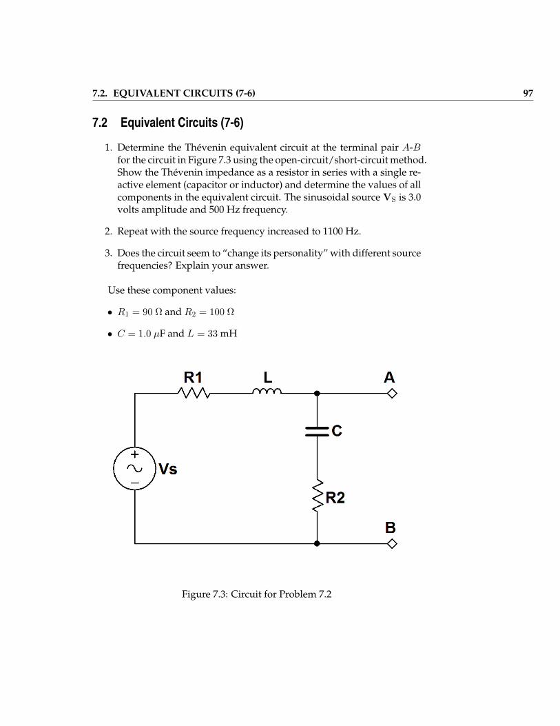
7.2. EQUIVALENT CIRCUITS (7-6) 97
7.2 Equivalent Circuits (7-6)
1. Determine the Thevenin equivalent circuit at the terminal pair A-Bfor the circuit in Figure 7.3 using the open-circuit/short-circuit method.Show the Thevenin impedance as a resistor in series with a single re-active element (capacitor or inductor) and determine the values of allcomponents in the equivalent circuit. The sinusoidal source VS is 3.0volts amplitude and 500 Hz frequency.
2. Repeat with the source frequency increased to 1100 Hz.
3. Does the circuit seem to “change its personality” with different sourcefrequencies? Explain your answer.
Use these component values:
• R1 = 90 Ω and R2 = 100 Ω
• C = 1.0 µF and L = 33 mH
Figure 7.3: Circuit for Problem 7.2

98 CHAPTER 7. AC ANALYSIS
NI Multisim Measurements
1. Enter the circuit of Figure 7.3 on the previous page with an AC VOLTAGEsource. Set its “AC Analysis Magnitude” to 3 volts and leave the “ACAnalysis Phase” at its default zero value. Run a Simulate→ Analyses→ Single Frequency AC Analysis to measure the open-circuit voltagemagnitude and phase. Next, connect a 0.1 Ω resistor across the ter-minal pair A-B to approximate a short circuit and then measure themagnitude and phase of the short-circuit current through this smallresistor. Calculate the Thevenin voltage and Thevenin impedancefrom these measurements.
2. Repeat to obtain the open-circuit voltage and short-circuit current at1100 Hz.
Additional helpful tips:
• Name the net connected to Terminal A to make it easier to find in theAC Analysis “Outputs” tab.
• Choose “Magnitude/Phase” for the “Complex number format” op-tion.
NI Multisim video tutorials:
• Measure phasor voltage with a Single Frequency AC Analysis:http://youtu.be/SwYCsoOwfUs
• Display and change net names:http://youtu.be/0iZ-ph9pJjE
NI myDAQ Measurements
1. Construct the circuit of Figure 7.3 on the preceding page; do not in-clude resistor R1 as this device simply models the finite winding re-sistance of the physical inductor. Build an op amp voltage followerto strengthen the current drive of AO0 and use the voltage followeroutput as VS. Create the sinusoidal voltage with the NI ELVISmxFunction Generator. Measure the open-circuit voltage magnitude andphase, taking the source voltage VS as the phase reference. Con-nect a 10 Ω resistor across the terminal pair A-B to approximate ashort circuit. Measure the voltage across this resistor and divide byits measured resistance to obtain the short-circuit current magnitude

7.2. EQUIVALENT CIRCUITS (7-6) 99
and phase. Calculate the Thevenin voltage and Thevenin impedancefrom these measurements.
2. Repeat to obtain the open-circuit voltage and short-circuit current at1100 Hz.
Additional helpful tips:
• The function generator sets it amplitude in terms of “peak-to-peak”voltage; this is twice the amplitude of the sinusoid. Adjust this volt-age to yield a sinusoid with a 3-volt amplitude.
• Use the NI ELVISmx Oscilloscope to display VS on AI0 and the volt-age at Terminal A on AI1.
• The oscilloscope “Display Measurements” panel under the waveformdisplay measures the peak-to-peak voltage of the waveforms. Set thetimebase to display at least two cycles to ensure that the measurementis accurate. Display even more cycles to improve the accuracy andstability of the measurement.
• You may also use the cursors to measure the amplitude (peak value).
• Refer to Appendix F on page 179 to learn how to measure amplitudeand phase of a sinusoidal waveform.
NI myDAQ video tutorials:
• Function Generator (FGEN):http://decibel.ni.com/content/docs/DOC-12940
• Oscilloscope:http://decibel.ni.com/content/docs/DOC-12942
• Increase current drive of analog output (AO) channels with anop amp voltage follower:http://decibel.ni.com/content/docs/DOC-12665
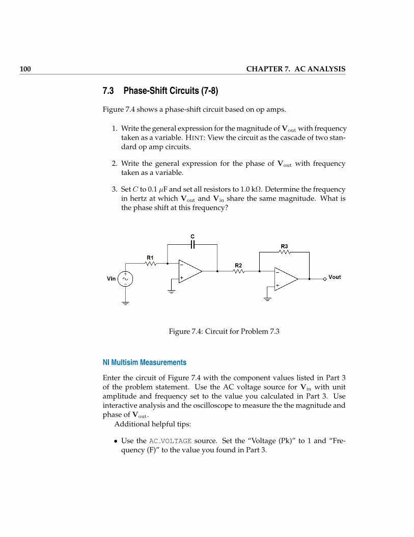
100 CHAPTER 7. AC ANALYSIS
7.3 Phase-Shift Circuits (7-8)
Figure 7.4 shows a phase-shift circuit based on op amps.
1. Write the general expression for the magnitude of Vout with frequencytaken as a variable. HINT: View the circuit as the cascade of two stan-dard op amp circuits.
2. Write the general expression for the phase of Vout with frequencytaken as a variable.
3. Set C to 0.1 µF and set all resistors to 1.0 kΩ. Determine the frequencyin hertz at which Vout and Vin share the same magnitude. What isthe phase shift at this frequency?
Figure 7.4: Circuit for Problem 7.3
NI Multisim Measurements
Enter the circuit of Figure 7.4 with the component values listed in Part 3of the problem statement. Use the AC voltage source for Vin with unitamplitude and frequency set to the value you calculated in Part 3. Useinteractive analysis and the oscilloscope to measure the the magnitude andphase of Vout.
Additional helpful tips:
• Use the AC VOLTAGE source. Set the “Voltage (Pk)” to 1 and “Fre-quency (F)” to the value you found in Part 3.

7.3. PHASE-SHIFT CIRCUITS (7-8) 101
• IMPORTANT: As a practical matter, connect a 100 kΩ resistor in par-allel with the capacitor to prevent the output of the first-stage circuitfrom saturating.
• Connect Simulate → Instruments → Oscilloscope so that you canview Vin and Vout at the same time.
• Use oscilloscope cursors to measure magnitude and phase with thetechnique described in Appendix F on page 179.
NI Multisim video tutorials:
• Basic operation of the two-channel oscilloscope:http://youtu.be/qnRK6QyqjvQ
• Waveform cursor measurements with the two-channel oscilloscope:http://youtu.be/snBRFq1Y1q4
NI myDAQ Measurements
Construct the circuit of Figure 7.4 on the preceding page with the compo-nent values listed in Part 3 of the problem statement. Use the NI ELVISmxFunction Generator to create the sinusoidal voltage source on AO0; set itsfrequency to the value you calculated in Part 3. Use the NI ELVISmx Oscil-loscope to measure the node voltages Vin and Vout.
Additional helpful tips:
• The function generator amplitude control uses “peak-to-peak” units.The amplitude of a sinusoid is one-half of its peak-to-peak value.
• IMPORTANT: As a practical matter, connect a 100 kΩ resistor in par-allel with the capacitor to prevent the output of the first-stage circuitfrom saturating.
• Use oscilloscope cursors to measure magnitude a phase with the tech-nique described in Appendix F on page 179.
NI myDAQ video tutorials:
• Function Generator (FGEN):http://decibel.ni.com/content/docs/DOC-12940
• Oscilloscope:http://decibel.ni.com/content/docs/DOC-12942

102 CHAPTER 7. AC ANALYSIS
7.4 Phasor-Domain Analysis Techniques (7-9)
The circuit of Figure 7.5 operates at 1 kHz. Determine the node voltagesVA and VB.
Use these component values:
• R1 = 4.7 kΩ, R2 = 3.3 kΩ and R3 = 2.2 kΩ
• C1 = 0.047 µF and C2 = 0.1 µF
• V1 = 9 6 0 V and V2 = 36 − 90 V
Figure 7.5: Circuit for Problem 7.4
NI Multisim Measurements
Enter the circuit of Figure 7.5 and run an AC analysis to measure the voltagemagnitude and phase of VA and VB.
More specifically:
• Use the AC VOLTAGE source. Set the “AC Analysis Magnitude” and“AC Analysis Phase” values according to the specified voltage sourcevalues.
• Set up an Simulate → Analyses → AC Analysis to sweep the fre-quency over a range that includes 1 kHz; use a “Linear” sweep typewith “Vertical Scale” set to “Linear.”

7.4. PHASOR-DOMAIN ANALYSIS TECHNIQUES (7-9) 103
• Use the “Grapher View” cursors to measure the voltage magnitudeand phase at 1 kHz.
NI Multisim video tutorials:
• Measure frequency response with AC Analysis:http://youtu.be/tgCPDBtRcso
• Find the maximum value of trace in Grapher View:http://youtu.be/MzYK60mfh2Y
NI myDAQ Measurements
Construct the circuit of Figure 7.5 on the preceding page. Use the NI ELVISmxArbitrary Waveform Generator to create the sinusoidal voltage sources; useAO0 to create V1 and AO1 to create V2. Use the NI ELVISmx Oscilloscopeto measure the node voltages VA and VB. Take V1 as the reference voltagewhen measuring phase.
Additional helpful tips:
• Set the Arbitrary Waveform Generator sampling rate to its maximumvalue of 200 kHz.
• Create a single period of a unit-amplitude 1 kHz sinusoid for eachoutput channel. Adjust the phase of the AO1 channel to match thephase of V2.
• Set the “Gain” controls of the Arbitrary Waveform Generator to matchthe magnitudes of the specified voltage sources.
• Refer to Appendix F to learn how to use the oscilloscope to measuremagnitude and phase.
NI myDAQ video tutorials:
• Arbitrary Waveform Generator (ARB):http://decibel.ni.com/content/docs/DOC-12941
• Oscilloscope:http://decibel.ni.com/content/docs/DOC-12942

104 CHAPTER 7. AC ANALYSIS
Chapter 8
AC Power
8.1 Periodic Waveforms (8-1)
Merriam-Webster defines a rectifier as a “device for converting alternatingcurrent into direct current.” A half-wave rectifier does so by setting the neg-ative portion of the waveform to zero. A full-wave rectifier negates the neg-ative portion of the waveform, effectively reflecting it to its positive equiv-alent.
1. Plot the half-wave rectifier output and full-wave rectifier output foreach of the three standard waveforms shown in Figure 8.1 on page 109.
2. Determine the general expressions for the (a) average value and (b)rms value for each of the six rectified waveforms.
3. Evaluate your expressions for average and rms values for Vm = 10 voltsand T = 10 ms.
NI Multisim Measurements
1. Create the half-wave rectified and full-wave rectified versions of thethree standard waveforms of Figure 8.1 on page 109 using the follow-ing approach:
• Create the unrectified original waveform with the Function Gen-erator,

106 CHAPTER 8. AC POWER
• Connect a wire to the + terminal of the function generator anddouble-click to terminate the wire in “empty space” without con-necting to any other terminal. Display the net names to deter-mine the number of this net. Connect the Common terminal toground.
• Place the ABM VOLTAGE source, ground its negative terminal,and enter the function positive(v(n)) (where n is the netnumber of the wire connected to the function generator output)to make the ABM source create the half-wave rectified versionof the function generator waveform,
• Place another ABM source (also with its negative terminal grounded)with the absolute value function abs(v(n)) to create the full-wave rectified waveform, and
• Place an SPDT switch (single-pole double-throw) to convenientlyconnect one ABM source or the other to the oscilloscope to dis-play the rectified waveform.
2. Place a Measurement Probe to display the average value and rmsvalue of the rectified waveform. Determine the average and rms val-ues of each of the rectified waveforms.
Additional tips:
• The “Analog Behavior Modeling” (ABM) voltage source “senses” thevoltage of net n with the function v(n). The connection between thefunction generator and the ABM source does not appear visually.
• The Multisim User Manual describes a wide variety of functions thatcan be used by the ABM source. Visit ni.com/manuals and enter“Multisim User Manual” into the search box. See the “MathematicalExpressions” section of Chapter 7.
• Set up the Simulate→ Instruments→ Measurement Probe to displayV(dc) for average value and V(rms) for rms value.

8.1. PERIODIC WAVEFORMS (8-1) 107
NI Multisim video tutorials:
• Display and change net names:http://youtu.be/0iZ-ph9pJjE
• Measure RMS and average value with a measurement probe:http://youtu.be/OnK-Unld17E
• Set the digits of precision of a measurement probe:http://youtu.be/GRO60XLgzHg
• ABM (Analog Behavioral Model) voltage source:http://youtu.be/8pPynWRwhO4
NI myDAQ Measurements
1. Create the half-wave rectified and full-wave rectified versions of thethree standard waveforms of Figure 8.1 on page 109 with the arbitrarywaveform generator on AO0; use 200 kS/s for the sampling rate. Dis-play this signal on the oscilloscope using AI0. Extract the averagevalue of the waveform using the RC circuit shown in Figure 8.2 onpage 110 and display the output of this circuit on AI1.
2. Read the average value of the rectified waveform using either the cur-sor value or the “RMS” indicator below the waveform display for AI1.Read the “RMS” indicator for AI0 to measure the rms value of therectified waveform. Display at least two periods of the waveform toensure accuracy of the “RMS” indicator.
Additional helpful tips:
• Set both channels of the oscilloscope to the same volts per division.In this way the RC circuit output (average value) overlays the recti-fied waveform and you can visually see how the average value tendstoward the effective center of the waveform.
• IMPORTANT: Be sure to observe proper polarity for the electrolyticcapacitor. The capacitor may mark the negative lead rather than thepositive lead.

108 CHAPTER 8. AC POWER
NI myDAQ video tutorials:
• Arbitrary Waveform Generator (ARB):http://decibel.ni.com/content/docs/DOC-12941
• Oscilloscope:http://decibel.ni.com/content/docs/DOC-12942

8.1. PERIODIC WAVEFORMS (8-1) 109
Figure 8.1: Waveforms for Problem 8.1

110 CHAPTER 8. AC POWER
Figure 8.2: RC circuit to extract average value of a waveform.

8.2. AVERAGE POWER (8-2) 111
8.2 Average Power (8-2)
The circuit shown in Figure 8.3 operates in sinusoidal steady state at 1500 Hz.The voltage source amplitude is 3 volts. Find the average power deliveredby the voltage source.
Use these component values:
• R = 100 Ω,
• C = 1.0 µF, and L = 3.3 mH
Figure 8.3: Circuit for Problem 8.2
NI Multisim Measurements
Enter the circuit of Figure 8.3 with an AC VOLTAGE source, setting its peakvalue and frequency according to the values specified in the problem state-ment. Place a Simulate→ Instruments→Wattmeter instrument to measurethe voltage source power. The wattmeter displays average power in sinu-soidal steady state.

112 CHAPTER 8. AC POWER
NI Multisim video tutorials:
• Measure average power and power factor with a wattmeter:http://youtu.be/kYliPwbWInc
NI myDAQ Measurements
Build the circuit of Figure 8.3 on the preceding page. Activate the circuitwith the NI ELVISmx Function Generator on AO0, and place an op ampvoltage follower between AO0 and the remaining circuit; the voltage fol-lower is necessary to boost the current drive of the analog output beyondits limit of 2 mA.
Use the NI ELVISmx Oscilloscope to display the voltage source on AI0;this voltage serves as the reference sinusoid for phase measurement. Dis-play the voltage across the resistor on AI1, and realize that this voltage isproportional to the voltage source current.
Calculate average power from three measurements: voltage source mag-nitude, current magnitude, and the phase difference between the sourcevoltage and current.
Additional helpful tips:
• The oscilloscope numerical display shows the RMS voltage of thewaveforms. Use the appropriate equation for average power basedon these RMS voltages.
• The oscilloscope numerical display also shows the peak-to-peak volt-age of the waveforms. One half of this value is the amplitude of asinusoidal waveform. If you choose this measurement, use the ap-propriate equation for average power based on amplitudes.
• Refer to Figure F on page 179 to learn how to measure amplitude andphase of a sinusoidal waveform.
NI myDAQ video tutorials:
• Increase current drive of analog output (AO) channels with anop amp voltage follower:http://decibel.ni.com/content/docs/DOC-12665
Further Exploration with NI myDAQ
The power delivered by the voltage source depends on it frequency:

8.2. AVERAGE POWER (8-2) 113
1. Monitor the voltage source current on the oscilloscope and adjust thevoltage source frequency to maximize the current amplitude, therebymaximizing the average source power delivered to the circuit. Recordthe voltage source frequency fmax at which the source average poweris maximized, and then calculate the average power delivered by thesource at this frequency.
2. Calculate the impedance of the inductor and capacitor at fmax. Ex-plain how these impedance values relate to maximizing the averagepower delivered by the source.
3. Adjust the voltage source frequency in a range above and below fmax
and observe the phase difference between the source voltage and cur-rent. Discuss your observations.

114 CHAPTER 8. AC POWER
8.3 Complex Power (8-3)
The circuit shown in Figure 8.4 operates in sinusoidal steady state at 1000 Hz.The voltage source amplitude is 2.5 volts.
1. Find the complex power in rectangular format for each of the fourcircuit elements: SSRC, SR, SL, and SC.
2. Demonstrate conservation of complex power with these four values.
Use these component values:
• R = 100 Ω, C = 1.0 µF, and L = 3.3 mH
Figure 8.4: Circuit for Problem 8.3
NI Multisim Measurements
Enter the circuit of Figure 8.4 with an AC VOLTAGE source. Set the “ACAnalysis Magnitude” parameter to match the amplitude specified in theproblem statement.

8.3. COMPLEX POWER (8-3) 115
1. Run a Simulate → Analyses → Single Frequency AC Analysis to de-termine the complex powers SSRC, SR, SL, and SC in rectangular for-mat.
2. Demonstrate conservation of complex power with these four values.
Additional helpful tips:
• The single-frequency AC analysis calls element power “P” (whichsuggests average power only) but in fact calculates complex power“S.”
NI Multisim video tutorials:
• Measure phasor voltage with a Single Frequency AC Analysis:http://youtu.be/SwYCsoOwfUs
NI myDAQ Measurements
Build the circuit of Figure 8.4 on the facing page. Activate the circuit withthe NI ELVISmx Function Generator on AO0, and place an op amp voltagefollower between AO0 and the remaining circuit; the voltage follower isnecessary to boost the current drive of the analog output beyond its limitof 2 mA.
Use the NI ELVISmx Oscilloscope to display the device voltage on AI0.Display the voltage across resistor R on AI1, and realize that this voltage isproportional to the current through every device in the circuit.
1. Measure the complex power for each of the four circuit elements us-ing the following procedure:
• Read the RMS voltage Vrms from the oscilloscope numerical dis-play,
• Read the RMS current Irms from the oscilloscope numerical dis-play (divide the measured voltage by the resistance R),
• Measure the time shift between the voltage and current sinu-soids with the oscilloscope cursors,
• Convert time shift to phase angle φZ = φv − φi (see Appendix Fon page 179 for details),
• Note whether the current waveform lags or leads the voltage; φZis positive when current lags and negative when current leads,

116 CHAPTER 8. AC POWER
• Express complex power as S = VrmsIrms 6 φZ , and
• Convert S to rectangular form.
2. Demonstrate conservation of complex power with these four values.
Additional helpful tips:
• Observe passive sign convention for each circuit element when mea-suring voltage and current: positive current enters the positive polar-ity terminal.
• Refer to Figure F on page 179 to learn how to measure amplitude andphase of a sinusoidal waveform.
NI myDAQ video tutorials:
• Increase current drive of analog output (AO) channels with anop amp voltage follower:http://decibel.ni.com/content/docs/DOC-12665

8.4. THE POWER FACTOR (8-4) 117
8.4 The Power Factor (8-4)
The circuit shown in Figure 8.5 on the next page is a “scale model” of twoindustrial electric motors and a heating unit connected to a manufactur-ing plant power distribution network. The resistor/inductor combinationsR1-L1 and R2-L2 model the winding resistance and magnetic fields of themotors. Resistor R3 models the heater coils. C represents the power factorcompensation equipment – essentially a capacitor bank with high powercapacity.
1. Determine the power factor of the uncompensated load, and draw itspower triangle to scale.
2. Determine the value of the compensation capacitor C required to im-prove the load power factor to 0.90 lagging.
3. Available power factor compensation capacitors include 0.1 µF, 1.0 µF,and 10 µF; the cost of compensation equipment increases with capaci-tance. Choose the least expensive compensation capacitor closest toCand then determine the power factor and power triangle (also drawnto scale) of the compensated load.
Use these component values:
• R1 = 10 Ω, R2 = 100 Ω, and R3 = 100 Ω
• L = 3.3 mH and L = 33 mH
• VSRC with 1 volt amplitude and 2500 Hz frequency (actual industrialmotors operate at hundreds of volts and 50 Hz to 60 Hz frequency)
NI Multisim Measurements
Enter the circuit of Figure 8.5 on the following page with an AC VOLTAGEsource, setting its peak value and frequency according to the values spec-ified in the problem statement. Place a SPST switch to conveniently en-gage or disengage the power factor compensation capacitor. Connect awattmeter to measure the power factor of the combined load and capac-itor.
IMPORTANT: Reduce the interactive simulation maximum time stepTMAX to 1e-006 seconds; find this parameter at Simulate → Interactive

118 CHAPTER 8. AC POWER
Figure 8.5: Circuit for Problem 8.4
Simulation Settings. The default time step does not produce sufficient sam-ple points per period at the operating frequency in this problem to allowthe wattmeter to produce an accurate power factor measurement.
1. Measure the power factor of the uncompensated load (switch open).
2. Close the switch to engage the compensation capacitor.
3. Measure the power factor of the compensated load.
NI Multisim video tutorials:
• Measure average power and power factor with a wattmeter:http://youtu.be/kYliPwbWInc
NI myDAQ Measurements
Build the circuit of Figure 8.5. Do not place resistors R1 and R2, as thesesimply model the finite winding resistances of the two inductors.
Activate the circuit with the NI ELVISmx Function Generator on AO0,and place an op amp voltage follower between AO0 and the remaining

8.4. THE POWER FACTOR (8-4) 119
circuit; the voltage follower boosts the current drive of the analog outputbeyond its limit of 2 mA.
Use the NI ELVISmx Oscilloscope to display the load voltage on AI0.Place a 10 Ω shunt resistor between the op amp output and the remainingcircuit; display the voltage across this shunt resistor on AI1, and recognizethat its voltage is proportional to the load current.
1. Measure the power factor of the uncompensated load.
2. Place your selected compensation capacitor into the circuit.
3. Measure the power factor of the compensated load.
Additional helpful tips:
• Place the myDAQ AI1 connections with proper polarity to measurepositive current flowing into the load.
• Recall that the power factor is cos(φZ) where φZ = φv −φi, the differ-ence between the load’s voltage phase and current phase.
• Refer to Appendix F on page 179 to learn how to measure the phaseof a sinusoidal waveform.
NI myDAQ video tutorials:
• Increase current drive of analog output (AO) channels with anop amp voltage follower:http://decibel.ni.com/content/docs/DOC-12665
Further Exploration with NI myDAQ
Long-haul electrical energy distribution networks rely on transformers toboost the voltage to hundreds of thousands of volts while simultaneouslyreducing the current to very low levels – remember that power is the prod-uct of voltage and current, hence a given power can be transferred with lowvoltage and high current or vice versa. Reducing the current reduces theresistive losses in the transmission wires and improves efficiency.
Experience how power factor compensation impacts the amount of cur-rent that the utility must supply to the customer’s equipment:
1. Measure and record the RMS voltage and current as displayed on theoscilloscope for the uncompensated load.

120 CHAPTER 8. AC POWER
2. Repeat these measurements for the compensated load.
3. Discuss which values remain similar and which values change signif-icantly. Comment on the value of power factor compensation as faras energy transmission efficiency is concerned.

Chapter 9
Frequency Response of Circuits andFilters
9.1 Scaling (9-2)
Figure 9.1 on the next page shows a prototype bandreject filter with centerfrequency ω0 = 1 rad/s. The prototype component values are R = 1 Ω,L = 1.817 H, and C = 0.5505 F.
1. Apply magnitude and frequency scaling to the bandreject filter sothat R′ = 100Ω and L′ = 33 mH. Draw the finished circuit diagram.
2. Determine the center frequency in hertz of the scaled bandreject filter.
NI Multisim Measurements
1. Enter the circuit of Figure 9.1 on the following page using the scaledcomponent values calculated earlier. Drive the filter input with anAC VOLTAGE source with “AC Analysis Magnitude” set to 1 V.
2. Plot the frequency response of the filter over the range 100 Hz to10 kHz with Simulate → Analyses → AC Analysis. Change “Verti-cal Scale” to “Linear” and increase “Number of points per decade”as needed to plot a smooth curve. Use a cursor to identify the filter’scenter frequency.

122 CHAPTER 9. FREQUENCY RESPONSE OF CIRCUITS AND FILTERS
Figure 9.1: Circuit for Problem 9.1
NI Multisim video tutorials:
• Measure frequency response with AC Analysis:http://youtu.be/tgCPDBtRcso
NI myDAQ Measurements
1. Build the circuit of Figure 9.1 using the scaled component values cal-culated earlier. Drive the filter input with AO0 strengthened by anop amp voltage follower. Monitor the filter input with AI0 and thefilter output with AI1.
2. Plot the frequency response of the filter over the range 100 Hz to10 kHz with the ELVISmx Bode Analyzer. Change “Mapping” to“Linear” and increase “Steps” as needed to plot a smooth curve. Usea cursor to identify the filter’s center frequency.
9.1. SCALING (9-2) 123
NI myDAQ video tutorials:
• Bode Analyzer:http://decibel.ni.com/content/docs/DOC-12943
• Increase current drive of analog output (AO) channels with anop amp voltage follower:http://decibel.ni.com/content/docs/DOC-12665
Further Exploration with NI myDAQ
NI Multisim provides a way to compare simulated results and physicalmeasurement results from NI myDAQ on the same ELVISmx instrument.Study the video tutorial below to learn how to simultaneously display sim-ulated and measured frequency response on the ELVISmx Bode Analyzer,and then do the following:
1. Plot the frequency response of the simulated and physical circuit ofFigure 9.1 on the facing page using the scaled component values cal-culated earlier. Compare the two plots and discuss their similaritiesand differences.
2. The simulated circuit is a model of the physical circuit and may notcapture every phenomenon of the real circuit. Recall that an inductoris formed by hundreds of turns of very fine (small diameter) wire,consequently the small yet finite resistance per unit length adds up toform a significant resistance. Measure the resistance of your inductorwith the myDAQ DMM and then place a resistor with this value inseries with the ideal inductor in your Multisim circuit. Re-run thesimulator. Compare the two plots and discuss the performance of theimproved circuit model.
NI Multisim video tutorials:
• Combine Multisim simulation and myDAQ measurements in thesame instrument – Bode Analyzer:http://youtu.be/3UmTmUj4h1g

124 CHAPTER 9. FREQUENCY RESPONSE OF CIRCUITS AND FILTERS
9.2 Bode Plots (9-3)
1. Determine the voltage transfer function H(ω) of the filter circuit shownin Figure 9.2. Write your finished result in standard form suitable forcreating a Bode plot.
2. Substitute ω = 2πf to express the voltage transfer function in termsof oscillation frequency f in hertz.
3. Generate Bode magnitude and phase plots for H(f) using oscillationfrequency f as the independent variable. Use the following compo-nent values: R1 = 3.3 kΩ, R2 = 10 kΩ, C1 = 0.01 µF, and C2 = 0.1 µF.
4. Determine the following filter circuit properties by inspecting the Bodeplot:
(a) Low-frequency asymptotes for magnitude and phase
(b) High-frequency asymptotes for magnitude and phase
(c) Corner frequencies (this filter circuit has two such frequencies)
Figure 9.2: Circuit for Problem 9.2

9.2. BODE PLOTS (9-3) 125
NI Multisim Measurements
1. Enter the filter circuit of Figure 9.2 on the facing page. Drive the filterinput with an AC VOLTAGE source with “AC Analysis Magnitude” setto 1 V. Use the three-terminal virtual op amp model OPAMP 3T VIRTUAL.
2. Plot the frequency response of the filter over the range 10 Hz to 100 kHzwith Simulate → Analyses → AC Analysis. Set “Vertical Scale” to“Decibel” and “Sweep Type” to “Decade” to create a standard Bodeplot presentation of frequency response. Increase “Number of pointsper decade” as needed to plot a smooth curve.
3. Determine the following filter circuit properties by inspecting the fre-quency response plot with cursors:
(a) Low-frequency asymptotes for magnitude and phase
(b) High-frequency asymptotes for magnitude and phase
(c) Corner frequencies; look for a change of 3 dB in magnitude froman asymptote
NI Multisim video tutorials:
• Measure frequency response with AC Analysis:http://youtu.be/tgCPDBtRcso
NI myDAQ Measurements
1. Build the filter circuit of Figure 9.2 on the preceding page. Drive thefilter input with AO0. Monitor the filter input with AI0 and the filteroutput with AI1.
2. Plot the frequency response of the filter over the range 10 Hz to 10 kHzwith the ELVISmx Bode Analyzer; note that this frequency range omitsthe last decade compared to your analytical and simulation work. In-crease “Steps” as needed to plot a smooth curve. IMPORTANT: Set“Peak Amplitude” to 1 volt.
3. Determine the following filter circuit properties by inspecting the fre-quency response plot with cursors:
(a) Low-frequency asymptotes for magnitude and phase
(b) High-frequency asymptotes for magnitude and phase

126 CHAPTER 9. FREQUENCY RESPONSE OF CIRCUITS AND FILTERS
(c) Corner frequencies; look for a change of 3 dB in magnitude froman asymptote
Additional helpful tips:
• The low- and high-frequency phase asymptotes of any filter are al-ways integer multiples of 90. If the phase plot does not seem to flattenout enough, simply estimate the trend to the closest integer multipleof 90.
NI myDAQ video tutorials:
• Bode Analyzer:http://decibel.ni.com/content/docs/DOC-12943
Further Exploration with NI myDAQ
Use the technique described in the video tutorial below to simultaneouslydisplay the simulated and measured frequency response with the ELVISmxBode Analyzer. You may need to set “Op-Amp Signal Polarity” to “In-verted” to make the measured phase response overlay the simulated re-sponse.
Discuss the level of agreement between the two plots and explain anydiscrepancies you observe.
NI Multisim video tutorials:
• Combine Multisim simulation and myDAQ measurements in thesame instrument – Bode Analyzer:http://youtu.be/3UmTmUj4h1g

9.3. FILTER ORDER (9-5) 127
9.3 Filter Order (9-5)
The filter circuit shown in Figure 9.3 uses the component valuesR = 1.0 kΩand C = 1.0 µF.
1. Obtain an expression for H(ω) = Vo/Vi in standard form.
2. Substitute ω = 2πf to express H(ω) in terms of oscillation frequencyf in hertz.
3. Generate spectral plots for the magnitude and phase of H(f).
4. Determine the cutoff frequency fc.
Figure 9.3: Circuit for Problem 9.3
NI Multisim Measurements
1. Enter the circuit of Figure 9.3. Drive the filter input with an AC VOLTAGEsource with “AC Analysis Magnitude” set to 1 V.

128 CHAPTER 9. FREQUENCY RESPONSE OF CIRCUITS AND FILTERS
2. Plot the frequency response of the filter over the range 1 Hz to 10 kHzwith Simulate → Analyses → AC Analysis. Set “Vertical Scale” to“Decibel” and “Sweep Type” to “Decade” to create a standard Bodeplot presentation of frequency response. Increase “Number of pointsper decade” as needed to plot a smooth curve.
3. Use cursors to measure the cutoff frequency fc (look for a change of3 dB in magnitude).
NI Multisim video tutorials:
• Measure frequency response with AC Analysis:http://youtu.be/tgCPDBtRcso
NI myDAQ Measurements
1. Build the circuit of Figure 9.3 on the preceding page. Drive the filterinput with AO0. Monitor the filter input with AI0 and the filter outputwith AI1.
2. Plot the frequency response of the filter over the range 1 Hz to 10 kHzwith the ELVISmx Bode Analyzer. Increase “Steps” as needed to plota smooth curve.
3. Use cursors to measure the cutoff frequency fc (look for a change of3 dB in magnitude).
NI myDAQ video tutorials:
• Bode Analyzer:http://decibel.ni.com/content/docs/DOC-12943
Further Exploration with NI myDAQ
Listen to the output of the Bode Analyzer to develop a more intuitive feelfor its operation. Connect AO0 AGND to your headphones similar to theconnection pictured in Figure 4.3 on page 48; connect the filter output toboth the right and left channels for best listening (the middle ring of theaudio plug carries the right channel signal). Comment on your listeningexperience.
IMPORTANT – PROTECT YOUR HEARING!

9.3. FILTER ORDER (9-5) 129
Do NOT disturb your circuit connections while you are wearing earphones.Accidently shorting together circuit connections can produce a very loudand unexpected noise. Alternatively, use a speaker to listen to the ampli-fier output or hold the earphones some distance from your ears.

130 CHAPTER 9. FREQUENCY RESPONSE OF CIRCUITS AND FILTERS
9.4 Cascaded Active Filters (9-7)
A telephone line provides sufficient bandwidth (3 kHz) for intelligible voiceconversations, but human hearing has a much higher bandwidth, typically20 Hz to 20,000 Hz.
1. Design an active bandpass filter to mimic the bandwidth of a tele-phone line subject to the following constraints:
(a) Cascade a first-order active lowpass filter and a first-order activehighpass filter,
(b) Set the corner frequencies to 300 Hz and 3.0 kHz,
(c) Set the passband gain to 0 dB,
(d) Choose resistors in the range 1.0 kΩ to 100 kΩ, and
(e) Use a total of four fixed-value resistors and two fixed-value ca-pacitors selected from the parts listed in Appendix A on page 159.
Draw the schematic diagram of your finished design.
2. Predict the performance of your finished design by calculating thefollowing values:
(a) Low-frequency passband corner in hertz,
(b) High-frequency passband corner in hertz, and
(c) Passband gain in decibels.
NI Multisim Measurements
1. Enter your bandpass filter.
2. Plot the frequency response of the filter over the audio frequencyrange 20 Hz to 20 kHz with Simulate → Analyses → AC Analysis.Set “Vertical Scale” to “Decibel” and “Sweep Type” to “Decade” tocreate a standard Bode plot presentation of frequency response.
3. Evaluate the performance of your design by measuring the followingvalues:
(a) Low-frequency passband corner in hertz (move cursor to−3.0 dBand read its frequency),
(b) High-frequency passband corner in hertz, and

9.4. CASCADED ACTIVE FILTERS (9-7) 131
(c) Passband gain in decibels.
NI Multisim video tutorials:
• Measure frequency response with AC Analysis:http://youtu.be/tgCPDBtRcso
• Set cursor to a specific value:http://youtu.be/48sQja58I10
NI myDAQ Measurements
1. Build your bandpass filter. Drive the filter input with AO0. Monitorthe filter input with AI0 and the filter output with AI1.
2. Plot the frequency response of the filter over the audio frequencyrange 20 Hz to 20 kHz with the ELVISmx Bode Analyzer. Increase“Steps” as needed to plot a smooth curve.
3. Evaluate the performance of your design by measuring the followingvalues with cursors:
(a) Low-frequency passband corner in hertz (move cursor to -3.0 dBand read its frequency),
(b) High-frequency passband corner in hertz, and
(c) Passband gain in decibels.
Additional helpful tips:
• You can obtain more accuracy on the low- and high-frequency cor-ners by sweeping the frequency over a narrow range that bracketsthe frequency of interest and substantially increasing the number ofsweep steps.
NI myDAQ video tutorials:
• Bode Analyzer:http://decibel.ni.com/content/docs/DOC-12943
Further Exploration with NI myDAQ
Listen to the audible effects of your telephone line emulator:

132 CHAPTER 9. FREQUENCY RESPONSE OF CIRCUITS AND FILTERS
1. Remove the AO0 connection,
2. Connect your audio player’s output to your filter’s input using the3.5 mm stereo audio cable included with your NI myDAQ product;use test leads to connect the left channel similar to the connectionpictured in Figure 4.3 on page 48.
3. Connect your headphones to the filter output; connect the filter out-put to both the right and left channels for best listening (the middlering of the audio plug carries the right channel signal),
4. Play music through your filter, and
5. Compare the sound of the music “with filtering” and “without filter-ing” by temporarily shorting the high-pass filter capacitor and dis-connecting the low-pass filter capacitor. Comment on your listeningexperience.
IMPORTANT – PROTECT YOUR HEARING!Do NOT disturb your circuit connections while you are wearing ear-phones. Accidently shorting together circuit connections can producea very loud and unexpected noise. Alternatively, use a speaker to lis-ten to the amplifier output or hold the earphones some distance fromyour ears.
For more sophistication, use the DG413 analog switch to convenientlyengage or disengage the telephone line emulator under control of one ofthe myDAQ DIO digital outputs. Use one normally-open switch and onenormally-closed switch for single-line control of the two switches necessaryto engage/disengage the filter.

Chapter 10
Laplace Transform AnalysisTechniques
10.1 s-Domain Circuit Analysis (10-7)
1. Determine v(t) of the circuit shown in Figure 10.1 on the followingpage for t ≥ 0, given that the switch is opened at t = 0 after havingbeen closed for a long time. Use the following component values:Vsrc = 8 V, R1 = 470 Ω, R2 = 100 Ω, Rw = 90 Ω, C = 1.0 µF, andL = 33 mH.
2. Plot v(t) from 0 to 5 ms using a tool such as MathScript or MATLAB.Include hardcopy of the script used to create the plot.
3. Determine the following values for v(t):
(a) Initial value v(0),
(b) Final value of v(t),
(c) Minimum value of v(t), and
(d) Time to reach the minimum value of v(t).
NI LabVIEW video tutorials:
• Plot two functions of time:http://youtu.be/XQlAai1-YVc
• Take cursor measurements on a plot:http://youtu.be/bgK1p5O6OXc

134 CHAPTER 10. LAPLACE TRANSFORM ANALYSIS TECHNIQUES
Figure 10.1: Circuit for Problem 10.1
NI Multisim Measurements
1. Enter the circuit of Figure 10.1 using the same component valueslisted in the problem statement. Implement the switch with aVOLTAGE CONTROLLED SWITCH operated by a PULSE VOLTAGE sourceconfigured to open the switch at time 1 ms; this delay makes the ini-tial transition easier to see.
2. Plot v(t) from 0 to 5 ms with a Simulate → Analyses → Transientanalysis.
3. Use the Grapher View cursors to measure the following values forv(t):
(a) Initial value v(0),
(b) Final value of v(t),
(c) Minimum value of v(t), and
(d) Time to reach the minimum value of v(t).
Helpful tip for this problem:
• Remember that Multisim voltages are all node voltages, i.e., a voltagewith respect to ground. The voltage v(t) in this problem exists be-

10.1. S-DOMAIN CIRCUIT ANALYSIS (10-7) 135
tween two nodes, however. Name the nets on either side ofR2 (or dis-play their default net numbers), click “Add expression” in the “Out-put” tab of the transient analysis setup panel, and enter an expressionof the form “v(pos)-v(neg)” where pos and neg denote the twonet names that connect to R2 with positive and negative polarity; theexpression forms the mathematical difference between the two nodevoltages.
NI Multisim video tutorials:
• Pulse voltage source:http://youtu.be/RdgxVfr28C8
• Voltage-controlled switch:http://youtu.be/BaEBjhD4TOw
• Plot time-domain circuit response with Transient Analysis:http://youtu.be/waKnad_EXkc
• Display and change net names:http://youtu.be/0iZ-ph9pJjE
NI myDAQ Measurements
1. Construct the circuit of Figure 10.1 on the facing page using the fol-lowing components and NI ELVISmx instruments:
• One normally-closed Switch 2 contained in the Intersil DG413quad analog switch described in Appendix D on page 173.
• 8.0 volt source created with the LM317 variable voltage circuitof Figure B.2 on page 164.
• 1.0 µF electrolytic capacitor. IMPORTANT: Observe proper po-larity of the capacitor by connecting the negative terminal of thecapacitor to ground.
• AIO0 (Analog Output 0) to the “Logic Control” (switch control)input for Switch 2.
• AI0 (Analog Input 0) to display the switch control voltage forSwitch 2; connect AI0+ to the switch control input and connectAI0- to ground.
• AI1 (Analog Input 1) to display v(t).

136 CHAPTER 10. LAPLACE TRANSFORM ANALYSIS TECHNIQUES
• Function Generator to create the switch control waveform; setthe frequency to 100 Hz and adjust the amplitude and offset toplace the control waveform between 0 and 5 volts.• Oscilloscope to view the Switch 2 control waveform and the
voltage vt(t).
2. Display v(t) from 0 to 5 ms.
3. Use the oscilloscope cursor to measure the following values for v(t):
(a) Initial value v(0),(b) Final value of v(t),(c) Minimum value of v(t), and(d) Time to reach the minimum value of v(t).
NI myDAQ video tutorials:
• Function Generator (FGEN):http://decibel.ni.com/content/docs/DOC-12940
• Oscilloscope:http://decibel.ni.com/content/docs/DOC-12942
Further Exploration with NI myDAQ
Switching circuits such as the one in this problem generally demand highcurrent from the power supply for brief periods of time. These high-currentpulses can cause spikes on the supply line that could disrupt proper opera-tion of other connected devices such as digital microcontrollers. Connect-ing a capacitor between the power supply rail and ground provides a localsupply of temporary current for the switching circuit to stabilize the powersupply rail for other devices.
1. Observe the VSRC rail created by the LM317 on the oscilloscope; itshould still be set to 8.0 V. Estimate the magnitude of the voltage spikeand express its value as a percentage of 8.0 V.
2. Continue to observe the power supply rail as you connect a 10 µF ca-pacitor between the VSRC rail and ground; place the capacitor in closeproximity to the switching circuit and remember to observe its po-larity. Discuss the improvement in the stability of the power supplyrail.

10.2. STEP RESPONSE (10-8) 137
10.2 Step Response (10-8)
1. Determine the transfer function H(s) = Vo(s)/Vs(s) of the circuitshown in Figure 10.2 on the next page. Write the transfer function insimplified standard form with symbolic values.
2. Determine the output response vo(t) to the input vs(t) = 4u(t) byworking in the Laplace domain. Assume the capacitor is initially dis-charged.
3. Plot vs(t) and vo(t) on the same graph from 0 to 5 ms using a tool suchas MathScript or MATLAB for R = 5.6 kΩ and C = 0.1 µF. Includehardcopy of the script used to create the plot.
4. Determine the following values for vo(t):
(a) Initial value vo(0+),
(b) Time to reach 50% of the initial value, and
(c) Final value.
NI Multisim Measurements
1. Enter the circuit of Figure 10.2 on the following page using the samecomponent values listed in the problem statement. Drive the circuitinput with a PULSE VOLTAGE source configured to produce vs(t) =4u(t). Delay the pulse by 1 ms to make the initial step transition visi-ble.
2. Plot vs(t) and vo(t) on the same graph from 0 to 5 ms with a Simulate→ Analyses→ Transient analysis.
3. Use the Grapher View cursors to measure the following values forvo(t):
(a) Initial value vo(0+),
(b) Time to reach 50% of the initial value, and
(c) Final value.

138 CHAPTER 10. LAPLACE TRANSFORM ANALYSIS TECHNIQUES
Figure 10.2: Circuit for Problem 10.2
NI Multisim video tutorials:
• Pulse voltage source:http://youtu.be/RdgxVfr28C8
• Plot time-domain circuit response with Transient Analysis:http://youtu.be/waKnad_EXkc
NI myDAQ Measurements
1. Build the circuit of Figure 10.2 using the same component valueslisted in the problem statement. Drive the circuit input with AO0 anduse the ELVISmx Function Generator to produce a zero-to-four voltstep transition with a period of 10 ms. Monitor the input voltage vs(t)with AI0 and the output voltage vo(t) with AI1.
2. Display vs(t) and vo(t) on the ELVISmx Oscilloscope.
3. Use the oscilloscope cursors to measure the following:

10.2. STEP RESPONSE (10-8) 139
(a) Initial value vo(0+),
(b) Time to reach 50% of the initial value, and
(c) Final value.
NI myDAQ video tutorials:
• Function Generator (FGEN):http://decibel.ni.com/content/docs/DOC-12940
• Oscilloscope:http://decibel.ni.com/content/docs/DOC-12942
Further Exploration with NI myDAQ
The circuit in this problem represents one implementation of an all-passfilter. Set up the ELVISmx Bode Analyzer to measure the frequency re-sponse of the circuit; the necessary myDAQ connections should already bein place. Set up the Bode analyzer controls as follows:
• Start frequency = 10 Hz
• Stop frequency = 10 kHz
• Steps = 10 per decade
• Mapping = linear
After running the frequency sweep set the “Gain” axis range to a minimumof zero and a maximum of 2; double-click the numerical values at the topand bottom of the axis display to set these values.
Study the response and then discuss the following questions:
1. Why is the circuit called an “all-pass” filter?
2. What is the general behavior of the phase response? More specifically,what are the maximum and minimum values of phase shift?
3. Use the cursor to measure the frequency at the midpoint between themaximum and minimum phase shift values. Compare this frequencyto the critical frequencies in the transfer function H(s) you derivedin the analytical section. HINT: Remember to account for angularfrequency versus oscillation frequency.

140 CHAPTER 10. LAPLACE TRANSFORM ANALYSIS TECHNIQUES
10.3 Transfer Function and Impulse Response (10-8)
Figure 10.3 shows a passive highpass filter circuit. After you determine itsbehavior (transfer function), design an input waveform to achieve a speci-fied output waveform shape; do the first three parts of this problem sym-bolically to maintain generality:
1. Determine the transfer function H(s) = Y(s)/X(s) of the circuit.
2. Determine and sketch the impulse response h(t) of the circuit.
3. Create an input waveform x(t) that will cause the output waveformy(t) to be a unit step function u(t). HINT: Work first in terms of H(s),Y(s), and X(s).
4. Plot x(t) and y(t) on the same graph from 0 to 100 ms using a tool suchas MathScript or MATLAB for R = 10 kΩ and C = 1.0 µF. Includehardcopy of the script used to create the plot.
5. Evaluate x(t) and y(t) at t = 50 ms.
Figure 10.3: Circuit for Problem 10.3

10.3. TRANSFER FUNCTION AND IMPULSE RESPONSE (10-8) 141
NI Multisim Measurements
1. Enter the circuit of Figure 10.3 on the preceding page using the samecomponent values listed in the analytical section. Drive the circuitinput with an ABM VOLTAGE source.
2. Plot x(t) and y(t) on the same graph from 0 to 100 ms with a Simulate→ Analyses→ Transient analysis.
3. Use the Grapher View cursors to measure the voltages x(t) and y(t)at t = 50 ms.
Additional Multisim tips for this problem:
• Build the ABM voltage source “Voltage Value” string by combiningone or more of the following functions:
– TIME – Time function t
– u(TIME) – Unit step function u(t)
– uramp(TIME) – Unit ramp function r(t)
– Standard math operators: +, -, *, and /
NI Multisim video tutorials:
• ABM (Analog Behavioral Model) voltage source:http://youtu.be/8pPynWRwhO4
• Plot time-domain circuit response with Transient Analysis:http://youtu.be/waKnad_EXkc
NI myDAQ Measurements
1. Build the circuit of Figure 10.3 on the facing page using the same com-ponent values listed in the analytical section. Drive the circuit inputwith AO0 and use the ELVISmx Arbitrary Function generator to pro-duce the waveform x(t) with a period of 100 ms. Set the voltage tozero before the end of the period to allow the circuit sufficient time toreturn to its zero-output state.
2. Display x(t) and y(t) on the ELVISmx Oscilloscope.
3. Use the oscilloscope cursors to measure the voltages x(t) and y(t) att = 50 ms.

142 CHAPTER 10. LAPLACE TRANSFORM ANALYSIS TECHNIQUES
NI myDAQ video tutorials:
• Arbitrary Waveform Generator (ARB):http://decibel.ni.com/content/docs/DOC-12941
• Oscilloscope:http://decibel.ni.com/content/docs/DOC-12942
Further Exploration with NI myDAQ
The impulse function δ(t) is physically unrealizable as an input voltagewaveform, however, it can be approximated by a large-valued short-durationrectangular pulse. Use the ELVISmx Arbitrary Waveform Generator to cre-ate a 10-volt pulse with very short duration compared to the 100 ms period.View this input waveform and the circuit’s output (an approximation to theimpulse response) on the oscilloscope. Discuss the similarity and differencebetween what you observe and what you calculated earlier as the circuit’sh(t).

10.4. CONVOLUTION INTEGRAL (10-9) 143
10.4 Convolution Integral (10-9)
Figure 10.4 shows a passive lowpass filter circuit and its input voltagewaveform x(t).
1. Determine the impulse response h(t) of the circuit; work this and thenext part with symbolic values.
2. Determine the output of the circuit y(t) = x(t) ∗ h(t) by integratingthe convolution analytically, i.e., use Method 2 of Example 10-15 inyour text. Carry out this step using symbolic values.
3. Plot x(t) and y(t) on the same graph from 0 to 100 ms using a toolsuch as MathScript or MATLAB for the following values: R = 10 kΩ,C = 1.0 µF, A = 5 volts, and t0 = 50 ms. Include hardcopy of thescript used to create the plot.
4. Evaluate y(t) at the following times: 25 ms, 50 ms, and 60 ms.
Figure 10.4: Circuit and input voltage waveform for Problem 10.4
NI Multisim Measurements
1. Enter the circuit of Figure 10.4 using the same component valueslisted in the problem statement. Drive the circuit input with an ABM VOLTAGEsource configured to produce the waveform x(t) with A = 5 voltsand t0 = 50 ms. Alternatively, use a PIECEWISE LINEAR VOLTAGEsource.

144 CHAPTER 10. LAPLACE TRANSFORM ANALYSIS TECHNIQUES
2. Plot x(t) and y(t) on the same graph from 0 to 100 ms with a Simulate→ Analyses → Transient analysis. Adjust the maximum time stepsetting to plot at least 100 time points.
3. Use the Grapher View cursors to measure the output voltage y(t) atthe times 25, 50, and 60 ms.
Additional Multisim tips for this problem:
• Build the ABM voltage source “Voltage Value” string by combiningthe following functions:
– TIME – Time function t
– u(TIME) – Step function u(t)
– Standard math operators: +, -, *, and /
NI Multisim video tutorials:
• ABM (Analog Behavioral Model) voltage source:http://youtu.be/8pPynWRwhO4
• Piecewise linear (PWL) voltage source:http://youtu.be/YYU5WuyebD0
• Plot time-domain circuit response with Transient Analysis:http://youtu.be/waKnad_EXkc
NI myDAQ Measurements
1. Build the circuit of Figure 10.4 on the previous page using the samecomponent values listed in the problem statement. Drive the circuitinput with AO0 and use the ELVISmx Arbitrary Waveform Generatorto produce the waveform shown in the same figure with A = 5 volts,and t0 = 50 ms. Set the period of the waveform to 100 ms.
2. Display x(t) and y(t) on the ELVISmx Oscilloscope.
3. Use the oscilloscope cursors to measure the output voltage y(t) at thetimes 25, 50, and 60 ms.

10.4. CONVOLUTION INTEGRAL (10-9) 145
NI myDAQ video tutorials:
• Arbitrary Waveform Generator (ARB):http://decibel.ni.com/content/docs/DOC-12941
• Oscilloscope:http://decibel.ni.com/content/docs/DOC-12942

146 CHAPTER 10. LAPLACE TRANSFORM ANALYSIS TECHNIQUES

Chapter 11
Fourier Analysis Techniques
11.1 Fourier Series Representation (11-2)
Consider the voltage waveform v(t) shown in Figure 11.1 on the followingpage.
1. Determine if the waveform has dc, even, or odd symmetry.
2. Obtain its cosine/sine Fourier series representation.
3. Convert the representation to amplitude format and plot the ampli-tude line spectrum for n = 0 to 5 using A = 10 volts and T = 4 ms.
NI Multisim Measurements
1. Create the voltage waveform v(t) of Figure 11.1 on the next pagewith a PIECEWISE LINEAR VOLTAGE source. Use the same ampli-tude and period as in the problem statement.
2. Plot and tabulate the amplitude line spectrum of v(t) with a Simulate→ Analyses→ Fourier Analysis :
(a) Set the “Frequency Resolution (fundamental frequency)” param-eter to match the fundamental frequency f0 of the voltage wave-form v(t).
(b) Leave the remaining parameters at their default settings.

148 CHAPTER 11. FOURIER ANALYSIS TECHNIQUES
Figure 11.1: Voltage waveform for Problem 11.1
NI Multisim video tutorials:
• Find commonly-used circuit components:http://youtu.be/G6ZJ8C0ja9Q
• Piecewise linear (PWL) voltage source:http://youtu.be/YYU5WuyebD0
NI myDAQ Measurements
1. Connect myDAQ Analog Output 0 to Analog Input 0, i.e., AO0 toAI0+ and AGND to AI0-.
2. Create the voltage waveform v(t) with the ELVISmx Arbitrary Wave-form Generator using the same amplitude and period as in the prob-lem statement. Set the sampling frequency to 200 kS/s.
3. Plot the power spectrum of v(t) on the ELVISmx Dynamic Signal An-alyzer (DSA). Carefully adjust the panel controls to match the follow-ing settings:
• Input Settings:
(a) Source Channel = AI0
(b) Voltage Range = +/-10V
• FFT Settings:

11.1. FOURIER SERIES REPRESENTATION (11-2) 149
(a) Frequency Span = 10000
(b) Resolution (lines) = 400
(c) Window = None
• Averaging:
(a) Mode = RMS
(b) Weighting = Exponential
(c) Number of Averages = 5
• Frequency Display:
(a) Units = Linear
(b) Mode = Peak
• Scale Settings:
(a) Scale = Auto
• Cursor Settings:
(a) Cursors On = enabled(b) Cursor Select = C1
4. Measure the amplitude spectrum for n = 0 to 5 using Cursor 1; takethe square root of the displayed cursor value “dVpkˆ2” to obtain thevoltage amplitude. IMPORTANT: Position Cursor 2 between a pair ofspectral lines to set its measured value to zero; the value displayedas dVpkˆ2 is the difference between the two cursors and you wantCursor 2 to serve as the zero reference.
Additional helpful tips:
• Use the cursor position buttons to make fine adjustments in the vicin-ity of a spectral line; these are the pair of gray diamonds at the bottomcenter of the DSA.
• Double-click the upper limit value on the horizontal frequency axisand select a lower value to zoom in on the lower-frequency spectrallines. Do not change the “Frequency Span” value for this purposebecause this changes the measurement itself.
NI myDAQ video tutorials:
• Arbitrary Waveform Generator (ARB):http://decibel.ni.com/content/docs/DOC-12941

150 CHAPTER 11. FOURIER ANALYSIS TECHNIQUES
Further Exploration with NI myDAQ
The ELVISmx Digital Signal Analyzer (DSA) represents a sophisticated in-strument that performs a wide variety of frequency-domain measurements.Experiment with the settings and discuss your findings:
• Averaging:
1. Choose Mode = Peak Hold and note that the “Restart” buttonlower down becomes active. Also try Mode = None.
2. Number of Averages: Try different values including 0.
• Frequency Display:
1. Choose Units = dB; what advantage do you see in a logarithmicdisplay compared to a linear display?
The “FFT Settings” control the Fast Fourier Transform computation thatserves as the heart of the DSA. These critical settings must be carefully se-lected to obtain correct amplitude spectrum measurements of periodic sig-nals. First learn how the DSA takes a measurement and then experimentwith the settings in a moment.
The DSA repetitively captures a snapshot of the input signal with du-ration “Resolution (lines)” (R) divided by “Frequency Span” (fspan); thistime-domain record appears below the frequency display. Take a momentto calculate this time duration from your current DSA FFT settings and con-firm that the value does indeed match the upper limit of the time-domainplot.
When measuring a periodic signal the captured time-domain signalmust contain an integer multiple of periods, consequently R/fspan dividedby the signal period T must be an integer N . Since the periodic signal fre-quency f0 is 1/T , the frequency span may be readily calculated as
fspan =Rf0N
, (11.1)
where fspan is the frequency span in Hz, R is the resolution in “lines” (sam-ple points), f0 is the fundamental frequency of the periodic input signal inHz, and N is the number of periods captured. N = 10 cycles provides agood starting point for most measurements.
Now, return the DSA settings to match those of your earlier work in theNI myDAQ section of this problem. Calculate the value of N . Also calcu-late the values of N that result from choosing the other available values for

11.1. FOURIER SERIES REPRESENTATION (11-2) 151
resolution R (the DSA offers a total of five resolutions). Change the DSAFFT resolution to each of the other available values, and note the effects onthe frequency spectrum display and on the time-domain display. In partic-ular, note the degree to which the amplitude line spectral values change.
Return the resolution to R = 400 lines. Calculate the frequency spanfspan for N = 10.5, i.e., for a time-domain record that contains ten periodswith a half-period tacked onto the end. Enter this value into the DSA andnote the degree to which the amplitude line spectral values change.

152 CHAPTER 11. FOURIER ANALYSIS TECHNIQUES
11.2 Circuit Applications (11-3)
The sawtooth voltage waveform vs(t) shown in Figure 11.2 with A = 5 Vand T = 2 ms serves as the input to the circuit of Figure 10.2 on page 138.
1. Determine the Fourier series representation of vo(t).
2. Plot vo(t) and vs(t) with MathScript or MATLAB as follows:
(a) Time 0 ≤ t ≤ 5 ms,(b) Sum of nmax = 100 terms, and(c) Circuit components R = 5.6 kΩ and C = 0.1 µF.
Use sufficient time resolution to display Gibbs phenomenon ringing.
3. Measure the maximum value of vo(t) from the plot, and also measurethe first time at which the maximum value occurs after t = 0.
Figure 11.2: Voltage waveform for Problem 11.2
NI LabVIEW video tutorials:
• Plot two functions of time:http://youtu.be/XQlAai1-YVc
• Take cursor measurements on a plot:http://youtu.be/bgK1p5O6OXc

11.2. CIRCUIT APPLICATIONS (11-3) 153
NI Multisim Measurements
1. Enter the circuit of Figure 10.2 on page 138 using the same componentvalues listed in the problem statement. Drive the circuit input witha TRIANGULAR VOLTAGE source configured with the amplitude andperiod specified in the problem statement.
2. Plot vo(t) and vs(t) using Simulate → Analyses → Transient analy-sis. Extend the plot time to 7 ms to allow the output to reach ACsteady-state. Increase the minimum number of time points as neededto produce a smooth plot.
3. Measure the maximum value of vo(t) with the Grapher View cursors,and also measure the first time at which the maximum value occursafter t = 0; ignore the transient start-up behavior during the firstperiod.
NI Multisim video tutorials:
• Find commonly-used circuit components:http://youtu.be/G6ZJ8C0ja9Q
• Plot time-domain circuit response with Transient Analysis:http://youtu.be/waKnad_EXkc
NI myDAQ Measurements
1. Build the circuit of Figure 10.2 on page 138 using the same componentvalues listed in the problem statement. Drive the circuit input withAO0 and use the ELVISmx Arbitrary Waveform Generator to producethe sawtooth waveform of Figure 11.2 on the facing page with theamplitude and period specified in the problem statement. Monitorthe input voltage vs(t) with AI0 and the output voltage vo(t) with AI1.
2. Display vs(t) and vo(t) on the ELVISmx Oscilloscope.
3. Use the oscilloscope cursors to measure the maximum value of vo(t)and the first time at which the maximum value occurs after t = 0.
NI myDAQ video tutorials:
• Arbitrary Waveform Generator (ARB):http://decibel.ni.com/content/docs/DOC-12941

154 CHAPTER 11. FOURIER ANALYSIS TECHNIQUES
11.3 Fourier Transform (11-5)
1. Determine the Fourier transform of the rectangular pulse f(t) shownin Figure 11.3.
2. Plot the amplitude spectrum |F(ω)| with MathScript or MATLAB asfollows:
(a) Frequency 0 ≤ f ≤ 4000 Hz (remember to convert angular fre-quency ω to oscillation frequency f ),
(b) A = 10, and
(c) τ = 1, 2, and 4 ms (create three distinct plots).
3. Determine the frequency at which the first null occurs in each of thethree plots.
4. Discuss the relationship between the rectangular pulse width and thewidth of the main lobe of the amplitude spectrum.
Figure 11.3: Rectangular pulse waveform for Problem 11.3

11.3. FOURIER TRANSFORM (11-5) 155
NI Multisim Measurements
1. Create a circuit with a PULSE VOLTAGE source. Set the “Period” to100 ms; set the remaining parameters as needed to create the pulseshown in Figure 11.3 on the facing page with A = 10. Note that thepulse must shift right to begin at t = 0; this shift does not affect theamplitude spectrum.
2. Plot the amplitude line spectrum of f(t) with a Simulate→ Analyses→ Fourier Analysis for τ = 1, 2, and 4 ms (create three plots). Set thefollowing parameter values:
• “Frequency Resolution (fundamental frequency)” = 10 Hz,
• “Number of harmonics” = 400,
• “Display” = “Graph,” and
• “Vertical scale” = “Linear.”
3. Determine the frequency at which the first null occurs in each of thethree plots.
NI Multisim video tutorials:
• Find commonly-used circuit components:http://youtu.be/G6ZJ8C0ja9Q
NI myDAQ Measurements
1. Set up your myDAQ and ELVISmx instruments as follows:
(a) Connect myDAQ Analog Output 0 to Analog Input 0, i.e., AO0to AI0+ and AGND to AI0-.
(b) Create the rectangular pulse f(t) with the ELVISmx FunctionGenerator in squarewave mode. Set the frequency to 10 Hz.Adjust the amplitude and DC offset controls to match the pulsewaveform shown in Figure 11.3 on the preceding page with A =10. Control the pulse width with the “Duty Cycle” control.
2. Plot the power spectrum of f(t) on the ELVISmx Dynamic Signal An-alyzer (DSA) for τ = 1, 2, and 4 ms (create three plots). Adjust thepanel controls to match the following settings:
• FFT Settings:

156 CHAPTER 11. FOURIER ANALYSIS TECHNIQUES
(a) Frequency Span = 4000
(b) Resolution (lines) = 400
(c) Window = None
• Averaging:
(a) Mode = None
• Frequency Display:
(a) Units = Linear
(b) Mode = Peak
• Scale Settings:
(a) Scale = Auto
3. Determine the frequency at which the first null occurs in each of thethree plots.
Further Exploration with NI myDAQ
1. Frequency spectrum plots normally possess much higher dynamic rangethan their corresponding time-domain plots. Review the DSA plotsyou created for the widest rectangular plot (τ = 4 ms), especially theside lobe amplitudes beyond the first null frequency. Note how theirvalues appear quite small compared to the amplitude of the mainlobe. Now set the “Frequency Display” units to “dB” (decibels); youcan stabilize the display by setting the “Scale Settings” from “Auto”to “Manual.” Discuss the merits of a logarithmic display scale com-pared to a linear display scale.
2. To further experience the advantages of a logarithmic display, repeatthe experiment with a single sinusoidal component. Set the functiongenerator to sinusoidal mode at 500 Hz and remove the DC offset.Display the spectrum with “Linear” units and then with “dB” units.Stabilize and improve the measurement by setting the “Averaging”mode to “RMS.” Discuss your observations.

11.4. CIRCUIT ANALYSIS WITH FOURIER TRANSFORM (11-8) 157
11.4 Circuit Analysis with Fourier Transform (11-8)
The circuit of Figure 11.4 is excited by the double-pulse waveform shownin the same figure.
1. Derive the expression for vo(t) using Fourier analysis.
2. Plot vs(t) and vo(t) on the same graph over the time span 0 ≤ t ≤ 5 mswith MathScript or MATLAB for the following values: A = 5 volt,T = 1 ms, R = 5.6 kΩ, and C = 0.1 µF.
3. Determine the value of vo(t) at times t = 2 ms and t = 3 ms.
Figure 11.4: Double-pulse waveform and circuit for Problem 11.4
NI Multisim Measurements
1. Enter the circuit of Figure 11.4 using an ABM VOLTAGE source and thecomponent values specified in the problem statement. Build the ABMvoltage source “Voltage Value” string with multiple step functionsu(TIME). Add, subtract, and delay the step functions as needed tocreate the double-pulse waveform of Figure 11.4 with the parametersspecified in the problem statement.

158 CHAPTER 11. FOURIER ANALYSIS TECHNIQUES
2. Set up a Simulate→ Analyses→ Transient to plot vs(t) and vo(t) overthe time span 0 ≤ t ≤ 5 ms. Choose “Set to zero” for the “Initial Con-ditions” parameter to properly model a discharged capacitor beforethe first pulse occurs. Increase the minimum time step as necessaryto obtain a smooth plot at discontinuities.
3. Use the Grapher View cursors to measure the value of vo(t) at timest = 2 ms and t = 3 ms.
NI Multisim video tutorials:
• Plot time-domain circuit response with Transient Analysis:http://youtu.be/waKnad_EXkc
• ABM (Analog Behavioral Model) voltage source:http://youtu.be/8pPynWRwhO4
NI myDAQ Measurements
1. Build the circuit of Figure 11.4 on the previous page using the com-ponent values specified in the problem statement. Drive the circuitwith the ELVISmx Arbitrary Waveform Generator on AO0. Create thedouble-pulse waveform of Figure 11.4 on the preceding page with theparameters specified in the problem statement. Monitor vs(t) on AI0and vo(t) on AI1.
2. Display vs(t) and vo(t) on the ELVISmx Oscilloscope. Adjust the set-tings for a time span of 5 ms and an appropriate scale (volts per di-vision) to clearly see the output trace behavior. Adjust the triggeringlevel and horizontal position to place the leading edge of the firstpulse at the far left of the display. You will likely need to use the“Run Once” acquisition mode to obtain a stable display; click “Run”repeatedly until you obtain a satisfactory display.
3. Use the oscilloscope cursors to measure the value of vo(t) at timest = 2 ms and t = 3 ms.
NI myDAQ video tutorials:
• Arbitrary Waveform Generator (ARB):http://decibel.ni.com/content/docs/DOC-12941

Appendix A
Parts List
Resistors
The following resistors are standard-value 5% tolerance 1/4 watt carbonfilm devices. All listed resistors are available in resistor kits from Digi-Key,Jameco, and RadioShack:
Resistor Kit Description Supplier Part #365 pcs, 5 ea of 1.0Ω to 1.0MΩ Digi-Key RS125-ND540 pcs, 30 values, 10Ω to 10MΩ Jameco 103166500 pcs, 64 values, 1.0Ω to 10MΩ RadioShack 271-312
See Resistor Color Codes at http://www.allaboutcircuits.com/vol_5/chpt_2/1.html to learn how to read the color bands on carbonfilm resistors.
Qty Value (Ω) Color Code1 10 Brown - Black - Black2 100 Brown - Black - Brown1 330 Orange - Orange - Brown1 470 Yellow - Violet - Brown1 680 Blue - Gray - Brown

160 APPENDIX A. PARTS LIST
Qty Value (kΩ) Color Code4 1.0 Brown - Black - Red1 1.5 Brown - Green - Red1 2.2 Red - Red - Red2 3.3 Orange - Orange - Red1 4.7 Yellow - Violet - Red4 5.6 Green - Blue - Red2 10 Brown - Black - Orange1 15 Brown - Green - Orange1 22 Red - Red - Orange1 33 Orange - Orange - Orange2 47 Yellow - Violet - Orange1 100 Brown - Black - Yellow
Potentiometers
The following potentiometers (variable resistors) are 3/8-inch square single-turn trimming style devices with 1/2-watt power rating.
Qty Description Digi-Key #1 100Ω trimpot (Bourns 3386P-1-501LF) 3386P-101LF-ND1 1K trimpot (Bourns 3386P-1-103LF) 3386P-102LF-ND2 10K trimpot (Bourns 3386P-1-103LF) 3386P-103LF-ND
Capacitors
Qty Value (µF) Type1 0.047 Ceramic1 0.01 Ceramic2 0.1 Ceramic1 1 Electrolytic1 10 Electrolytic

161
Inductors
Qty Description Digi-Key #1 3.3-mH inductor (Murata Power Solutions 22R335C) 811-1295-ND1 33-mH inductor (Murata Power Solutions 22R336C) 811-1294-ND
Active Devices and Integrated Circuits
NOTE: Texas Instruments offers free samples. Go to http://www.ti.comand click “Sample & Buy” to get started.
Qty Description Digi-Key #3 LM317L voltage regulator, 100mA (Texas Instruments) 296-17221-1-ND1 TL072CP dual op amp (Texas Instruments) 296-1775-5-ND1 DG413DJZ quad analog switch (Intersil) DG413DJZ-ND
Breadboard
Circuit Specialists part number WB-102, http://www.circuitspecialists.com/prod.itml/icOid/6885
Jumper Wire Kit
Circuit Specialists part number WK-1 (350 pieces, pre-formed, 22 AWG),http://www.circuitspecialists.com/prod.itml/icOid/6920
Circuit Specialists part number MJW-70B (140 pieces, pre-formed, 22 AWG),http://www.circuitspecialists.com/prod.itml/icOid/7590
Test Leads
Alligator clip style, cut in half with tinned ends.Circuit Specialists part number M000F0003, http://www.circuitspecialists.
com/prod.itml/icOid/7682

162 APPENDIX A. PARTS LIST

Appendix B
LM317 Voltage and Current Sources
The Texas Instruments LM317 adjustable voltage regulator is a flexible de-vice that when combined with suitable external resistors and the NI my-DAQ power supply can serve as the basis for a fixed or variable volt-age source and a fixed or variable current source. Figure B.1 shows theLM317 package terminals as well as its schematic symbol. The LM317sources current up to 1.5 amps, while the LM317L sources up to 100 mA.See the datasheets available at http://www.ti.com; enter “lm317” in the“Search by Part Number” field.
Figure B.1: LM317 adjustable voltage regulator: (a) package and terminalsfor 1.5-amp device (TO-220 package), (b) package and terminals for 100-mA device (TO-92 package), and (c) schematic symbol.

164 APPENDIX B. LM317 VOLTAGE AND CURRENT SOURCES
B.1 Variable Voltage Source
The circuit shown in Figure B.2 produces a variable voltage in the range1.5 V to 13.5 V from the NI myDAQ +15V power supply. Figure B.3 onthe next page shows the recommended breadboard layout for this circuit.Use bare-wire loops to facilitate easy connections with test leads to the NImyDAQ±15-volt dual power supply. The horizontal voltage “rails” followthe top-to-bottom order of high to low voltage: +15 volts, variable voltage,ground, and -15 volts. Build this circuit on the left edge of your breadboardand leave it in place for all of your circuits projects.
Figure B.2: LM317 as a variable voltage source: (a) schematic diagram and(b) equivalent circuit.
B.2 Current Source
The circuit shown in Figure B.4 on page 166 produces a current whose valueis approximately 1250/R mA. This circuit configuration “sources” current

B.2. CURRENT SOURCE 165
Figure B.3: Recommended breadboard layout for the LM317-based vari-able voltage source: (a) top view of breadboard showing the componentlayout and voltage rail order, and (b) side view showing test lead connec-tions between NI myDAQ and wire loops on the breadboard.
from the NI myDAQ +15V power supply and effectively operates as a cur-rent source with one terminal permanently attached to the NI myDAQ ana-log ground AGND.
The current source will operate as expected for circuits powered by theNI myDAQ ±15 V dual power supply provided the following conditionshold:
1. The requested current does not exceed the 30 mA current limit of theNI myDAQ +15V power supply,
2. The voltage of the ungrounded current source terminal does not risehigher than 13.5 V above ground, and
3. The current set resistor R does not exceed approximately 1.2 kΩ (theminimum current ISRC is approximately 1 mA).
Figure B.5 on page 167 illustrates a similar current source that “sinks”current to the NI myDAQ −15 V power supply. The current source willoperate as expected for circuits powered by the NI myDAQ ±15 V dualpower supply provided the following conditions hold:
1. The requested current does not exceed the 30 mA current limit of theNI myDAQ −15 V power supply,

166 APPENDIX B. LM317 VOLTAGE AND CURRENT SOURCES
Figure B.4: LM317 adjustable voltage regulator as a grounded currentsource sourcing current from the NI myDAQ +15V power supply: (a)schematic diagram, (b) equivalent circuit model, and (c) recommended lay-out with the standard breadboard layout of Figure B.3 on the precedingpage.
2. The voltage of the ungrounded current source terminal does not falllower than 13.5 V below ground, and
3. The current set resistor R does not exceed approximately 1.2 kΩ (theminimum current ISRC is approximately 1 mA).

B.2. CURRENT SOURCE 167
Figure B.5: LM317 adjustable voltage regulator as a grounded currentsource sinking current to the NI myDAQ -15V power supply: (a) schematicdiagram, (b) equivalent circuit model, and (c) recommended layout withthe standard breadboard layout of Figure B.3 on page 165.

168 APPENDIX B. LM317 VOLTAGE AND CURRENT SOURCES

Appendix C
TL072 Operational Amplifier
The Texas Instruments TL072 dual operational amplifier (“op amp”) pro-vides two op amp devices in a single 8-pin package. For more detailssee the datasheet available at http://www.ti.com; enter “tl072” in the“Search by Part Number” field.
Figure C.1 on the following page shows the pinout diagram for theTL072. Note the requirement for a dual power supply; the NI myDAQ±15 V supply serves this purpose. Also note that the op amp device it-self does not have a ground terminal. Instead the myDAQ AGND (analogground) establishes the ground reference.
Figure C.2 on page 171 shows the TL072 placed on the standard bread-board layout described in Figure B.3 on page 165, connected to power, andready for additional circuitry.
NI Multisim provides a circuit model for the TL072: place the TL072ACPdevice.
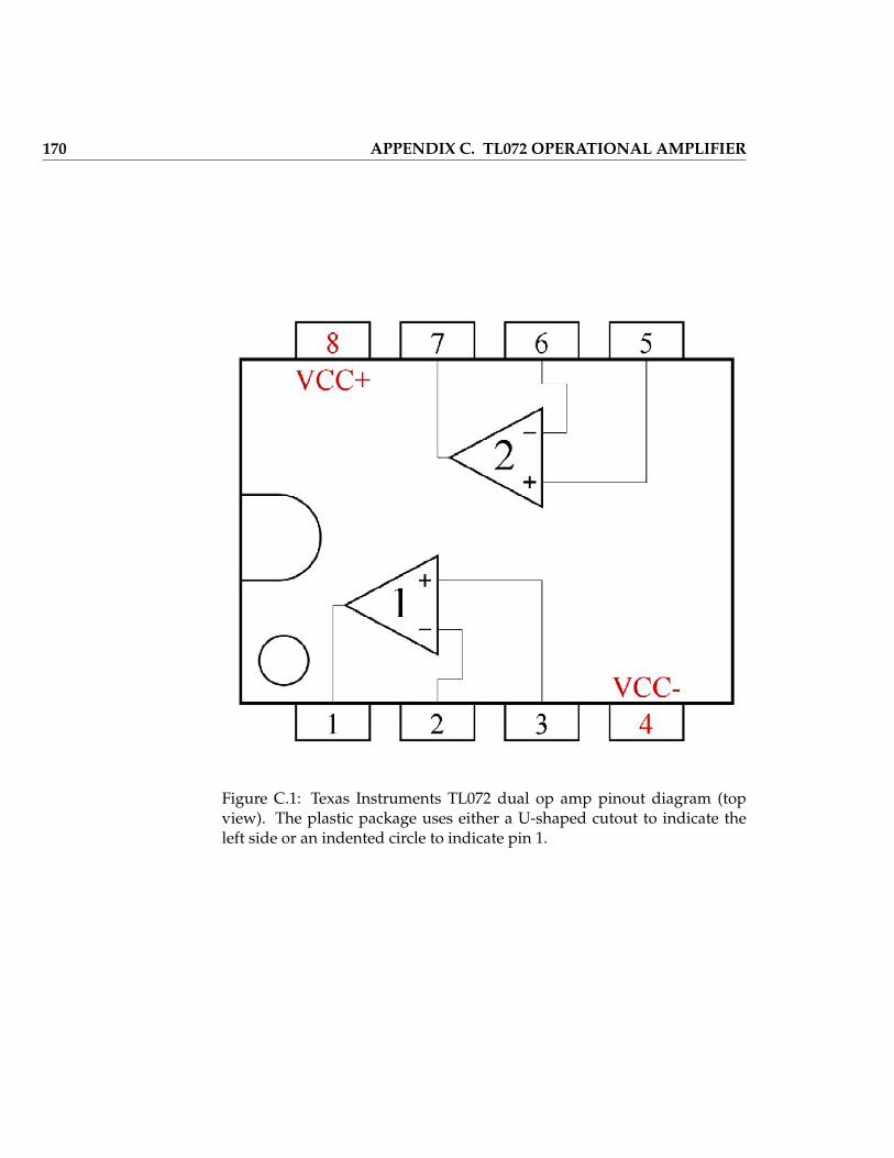
170 APPENDIX C. TL072 OPERATIONAL AMPLIFIER
Figure C.1: Texas Instruments TL072 dual op amp pinout diagram (topview). The plastic package uses either a U-shaped cutout to indicate theleft side or an indented circle to indicate pin 1.

171
Figure C.2: Texas Instruments TL072 dual op amp placed on the standardbreadboard layout, connected to power, and ready for additional circuitry.

172 APPENDIX C. TL072 OPERATIONAL AMPLIFIER

Appendix D
DG413 Quad Analog Switch
The Intersil DG413 provides four analog switches; refer to Figure D.1 on thenext page for the pinout diagram. Each switch is bidirectional and operatesjust like a physical SPDT switch but under the control of a digital (two-level) control signal. Two of the switches are normally-open and the othertwo switches are normally-closed. For more details see the datasheet avail-able at http://www.intersil.com; enter “dg413” in the search box.
When connected and powered as shown in Figure D.2 on page 175 theswitches operate as expected over the full ±15 V range under the controlof the myDAQ digital outputs DIO0 to DIO7. The analog outputs AO0 andAO1 may also serve as control signals provided they produce a voltage ofeither 0 V (inactive switch state) or 5 V (active switch state).
NI Multisim provides a circuit model for the DG413: place the ADG413BNdevice.

174 APPENDIX D. DG413 QUAD ANALOG SWITCH
Figure D.1: Intersil DG413 quad analog switch pinout diagram (topview).Two of the switches are normally-open and the other two switchesare normally-closed. The switch positions indicate the normal (inactive)state with the switch control voltage at low level. Switches 1 and 4 arenormally-open (NO) and Switches 2 and 3 are normally-closed (NC).

175
Figure D.2: Intersil DG413 quad analog switch placed on the standardbreadboard layout, connected to power, and ready for additional circuitry.

176 APPENDIX D. DG413 QUAD ANALOG SWITCH

Appendix E
Transient Response MeasurementTechniques
E.1 Time Constant
The general first-order circuit response takes the form
x(t) = x(∞) + [x(0)− x(∞)]e−t/τ , t ≥ 0, (E.1)
where x(0) is the initial value at the start of the transient, x(∞) is the finalvalue, and τ is the time constant. Figure E.1 on the next page plots thisequation for the case of a final value lower than the initial value. This fig-ure also shows the half-life time THL, defined as the time interval from theonset of the transient at time t = 0 to the time at which x(t) reaches themidpoint of the initial and final values. The half-life is easy to measure onan oscilloscope from which the time constant follows as
τ =THL
ln 2. (E.2)

178 APPENDIX E. TRANSIENT RESPONSE MEASUREMENT TECHNIQUES
Figure E.1: General first-order circuit response showing initial value, finalvalue, and half-life time.

Appendix F
Sinusoid Measurement Techniques
F.1 Amplitude and Phase Measurements
Figure F.1 shows a pair of sinusoidal signals as displayed on an oscillo-scope. The “Reference” sinusoid serves as the phase reference for the “Sig-nal of Interest” and has a phase of zero degrees. Both sinusoids oscillateat the same frequency f0. Three measurements suffice to determine thephasor representation of each sinusoid as follows:
Figure F.1: A pair of sinusoidal signals at the same frequency, one as thereference and the other as the signal of interest. A andB indicate amplitudemeasurements and C indicates the time shift measurement for phase.

180 APPENDIX F. SINUSOID MEASUREMENT TECHNIQUES
1. The reference sinusoid is A 6 0,
2. The phase shift θ in degrees is ±θ = C × f0 × 360 where C is theabsolute value of the time shift between the two sinusoids in secondsand f0 is sinusoidal frequency in Hz; choose positive sign when thesignal of interest leads the reference (its zero crossing occurs before thereference as pictured in Figure F.1 on the previous page) and negativesign otherwise, and
3. The signal of interest is B 6 θ.
Consider the NI ELVISmx Oscilloscope display of Figure F.2 on the fac-ing page as an example of this measurement technique. Note that the “Voltsper Division” scales have been adjusted to make both sinusoids fill as muchof the screen as possible. The green trace on Channel 0 serves as the refer-ence while the blue trace on Channel 1 is the signal of interest. The cursorshave been adjusted to measure the time shift between the two signals. Notethat the numerical display under the traces provides all necessary measure-ments:
1. The reference sinusoid amplitude is 1.696 volts divided by 2 (to con-vert from peak-to-peak) or 848 mV with a phase of zero degrees,
2. The phase shift is −65 µs × 2.502 kHz × 360 = −59; the phase isnegative because the signal of interest (blue trace) lags the reference,i.e., the zero crossing occurs after the zero crossing of the reference,and
3. The amplitude of the signal of interest is 427 mV divided by 2 or214 mV.
From these measurements the phasor form of the reference is 848 6 0mVand the phasor form of the signal of interest is 214 6 − 59 mV.

F.1. AMPLITUDE AND PHASE MEASUREMENTS 181
Figure F.2: A pair of sinusoidal signals at the same frequency measuredby the NI ELVISmx Oscilloscope. After adjusting the cursors to measuretime shift the numerical display provides all required information in thenumerical display area.

182 APPENDIX F. SINUSOID MEASUREMENT TECHNIQUES

Appendix G
Video Links
NI LabVIEW MathScript Video Tutorials
• Plot two functions of time:http://youtu.be/XQlAai1-YVc
• Take cursor measurements on a plot:http://youtu.be/bgK1p5O6OXc
NI Multisim & NI myDAQ Video Tutorials
• Compare simulated and physical DMM measurements:http://youtu.be/MZiZ_C-ngkY
NI Multisim Video Tutorials
Place components:
• Find commonly-used circuit components:http://youtu.be/G6ZJ8C0ja9Q
• Find components by name:http://youtu.be/5wlFweh4n-c
Sources:
• Function generator:http://youtu.be/CeOl6EzD-_c

184 APPENDIX G. VIDEO LINKS
• AC (sinusoidal) voltage source:http://youtu.be/CXbuz7MVLSs
• ABM (Analog Behavioral Model) voltage source:http://youtu.be/8pPynWRwhO4
• Pulse voltage source:http://youtu.be/RdgxVfr28C8
• Piecewise linear (PWL) voltage source:http://youtu.be/YYU5WuyebD0
• VDD and VSS power supply voltages:http://youtu.be/XrPVLgYsDdY
Measure DC current:
• Measure DC current with a measurement probe:http://youtu.be/uZ56byigymI
• Measure DC mesh current with a measurement probe:http://youtu.be/lK0LcTNroXI
• Measure DC current with an ammeter indicator:http://youtu.be/8P4oFw6sIzQ
Measure DC voltage:
• Measure DC voltage with a voltmeter:http://youtu.be/XLyslyikUws
• Measure DC voltage with a referenced measurement probe:http://youtu.be/xKEQ3EXEaP8
• Measure DC voltage with a voltmeter indicator:http://youtu.be/8h2SAZ9gkBA
• Set the digits of precision of a measurement probe:http://youtu.be/GRO60XLgzHg

185
Measure DC node voltage:
• Measure DC node voltage with a measurement probe:http://youtu.be/svNGHA2-uK4
• Find node voltages with DC Operating Point analysis:http://youtu.be/gXBCqP17AZs
Measure DC power:
• Measure DC power with a wattmeter:http://youtu.be/-axVClpMpiU
• Find resistor power with DC Operating Point analysis:http://youtu.be/NxXmVDW9spo
• Use a Parameter Sweep analysis to plot resistor power as a functionof resistance:http://youtu.be/3k2g9Penuag
Measure resistance:
• Measure resistance with an ohmmeter:http://youtu.be/3G5V0Hxjkbg
Measure RMS and average value:
• Measure RMS and average value with a measurement probe:http://youtu.be/OnK-Unld17E
Measure AC phasor voltage:
• Measure phasor voltage with a Single Frequency AC Analysis:http://youtu.be/SwYCsoOwfUs
Measure frequency response:
• Measure frequency response with AC Analysis:http://youtu.be/tgCPDBtRcso

186 APPENDIX G. VIDEO LINKS
Measure AC power:
• Measure average power and power factor with a wattmeter:http://youtu.be/kYliPwbWInc
Net names:
• Display and change net names:http://youtu.be/0iZ-ph9pJjE
Grapher View and oscilloscope cursor measurements:
• Find the maximum value of trace in Grapher View:http://youtu.be/MzYK60mfh2Y
• Set cursor to a specific value:http://youtu.be/48sQja58I10
Oscilloscope:
• Basic operation of the two-channel oscilloscope:http://youtu.be/qnRK6QyqjvQ
• Waveform cursor measurements with the two-channel oscilloscope:http://youtu.be/snBRFq1Y1q4
• Distinguish oscilloscope traces by color:http://youtu.be/bICbjggcTiQ
• Stabilize the oscilloscope display with edge triggering:http://youtu.be/d69zYYSEG7E
• Basic operation of the four-channel oscilloscope:http://youtu.be/iUqs_c1Bc4Y
Transient response:
• Plot time-domain circuit response with Transient Analysis:http://youtu.be/waKnad_EXkc
• Voltage-controlled switch:http://youtu.be/BaEBjhD4TOw

187
Combined Multisim / myDAQ measurements:
• Combine Multisim simulation and myDAQ measurements in the sameinstrument – Bode Analyzer:http://youtu.be/3UmTmUj4h1g
NI myDAQ Video Tutorials
See Electrical Circuits with NI myDAQ for more video tutorials and projects:http://decibel.ni.com/content/docs/DOC-12654
NI ELVISmx Instruments for NI myDAQ:
• DMM ohmmeter:http://decibel.ni.com/content/docs/DOC-12938
• DMM voltmeter:http://decibel.ni.com/content/docs/DOC-12937
• DMM ammeter:http://decibel.ni.com/content/docs/DOC-12939
• Function Generator (FGEN):http://decibel.ni.com/content/docs/DOC-12940
• Arbitrary Waveform Generator (ARB):http://decibel.ni.com/content/docs/DOC-12941
• Oscilloscope:http://decibel.ni.com/content/docs/DOC-12942
• Bode Analyzer:http://decibel.ni.com/content/docs/DOC-12943
• Digital Reader (DigIn):http://decibel.ni.com/content/docs/DOC-12944
• Digital Writer (DigOut):http://decibel.ni.com/content/docs/DOC-12945

188 APPENDIX G. VIDEO LINKS
Measurement techniques:
• Measure current with a shunt resistor and DMM voltmeter:http://decibel.ni.com/content/docs/DOC-12946
• Measure node voltage:http://decibel.ni.com/content/docs/DOC-12947
• Increase current drive of analog output (AO) channels with an op ampvoltage follower:http://decibel.ni.com/content/docs/DOC-12665