c 2009 guneeta singh bhalla - university of florida
TRANSCRIPT

SIZE EFFECTS IN PHASE SEPARATED MANGANITE NANOSTRUCTURES
By
GUNEETA SINGH BHALLA
A DISSERTATION PRESENTED TO THE GRADUATE SCHOOLOF THE UNIVERSITY OF FLORIDA IN PARTIAL FULFILLMENT
OF THE REQUIREMENTS FOR THE DEGREE OFDOCTOR OF PHILOSOPHY
UNIVERSITY OF FLORIDA
2009
1

c© 2009 Guneeta Singh Bhalla
2

To those individuals who seek to fulfill their curiosity about manganite nanostructures
3

ACKNOWLEDGMENTS
The doctoral process for me, as for those before me, has been a long term challenge
requiring strong support from many people in my life, both professionally and personally.
Below I will be liberal with the space I use to acknowledge some of the many people who
have lifted me up and helped me climb this mountain.
First and foremost, I am grateful to Dr. Arthur F. Hebard for supporting me
throughout the years and providing the haven of his laboratory for me to experiment
in freely. I have learned a tremendous amount in the years I have spent in his laboratory:
I have gone from zero to everything I now know about experimental physics.
Next I would like to thank a close collaborator, Dr. Amlan Biswas for teaching me
how to use the pulsed laser deposition (PLD) system and so much more on the topic of
manganites (and politics) and complex oxides in general. I would also like to thank my
collaborators in Japan, Dr. Harold Y. Hwang and Dr. Christopher Bell for being excellent
hosts during my stay and for their inspirational discussions on the topic of complex oxides.
I would like to thank my theoretical collaborators, Dr. Denis I. Golosov in Israel and Dr.
Selman Hershfield and his student Sara Joy for their patience and insightful theoretical
perspectives. I would also like to thank several other members of the UF Physics and
Material Science Department for taking the time to have discussions with me from which
I have learned a lot: Thank you Dr. Peter J. Hirshfeld, Dr. Dimitrii Maslov, Dr. David
Tanner, Dr. Pradeep Kumar, Dr. Juan Nino, Dr. Andrew Rinzler and Dr. Gerald Bourne.
I am also grateful to Dr. Katia Matcheva and Dr. Petkova for providing the support
and practical advise that is an essential ingredient for PhD students, but ironically almost
completely nonexistent. I feel lucky to have had it, so thank you!
I thank Xu Du, Sinan Selcuk, Sef Tongay, Bo Liu, Tara Dhakal and Patrick Mickel
for all their support, collaboration and discussions. I thank other present and previous
members of my laboratory and the UF physics department for their insights, friendship
and support: Thanks, Nikoleta Theodopolous, Sanal Buveav, Jay Horton, Sandra and
4

the night crew, H. J. Jeen and Dan Sindhikara (for motivating me to go to Japan). And
especially, a grand thanks to Corey Stambaugh and Jens for being my TeXsupport!
I thank my sister for showing me the importance of being humble and not too
possessive of one’s own creations.
I thank my parents for being supportive and liberal and letting me experience the
world (literally) on my own accord while I was still young and invincible. (Not sure if I’ll
ever again muster up the spirit to go wander through the Sahara). I thank my dad for his
unconditional love, support and acceptance of me for the person I am and for his humility.
I thank my mom for being an amazing role model and getting to the top of her career
purely through hard work and against all odds.
I thank my maternal uncle, my mamaji, for fueling my curiosity and trust by going
out of his way to answer all my questions, even if it took years. I also thank him for
sharing all those anecdotes and childhood bedtime stories of female warriors, scientists
and other heros that I still find myself recalling time and again for inspiration. I see the
importance now. Thanks to my grandparents, my naniji and nanaji, my cousins Blossom
and Tegbir, my aunt, my mamiji and Rajan for being such a supportive and loving family
that I can always come back to. Your presence has made it all possible.
I thank my wonderful friend Jens for spoiling me with delicious home cooked meals
to help minimize the thesis woes. I thank my best friend Marissa for those long phone
sessions and full support during the good and bad times. Thanks Nate Heston and Jordan
McCann for all those mountain adventures, Louise Laudermilk for those early morning
forest runs, Jagritee Sharma for the endless PhD anecdotes and Aaron Manalaysay, Shawn
Allgeier, Saiti Datta for keepin’ it real in the basement. I would also like to thank my old
friends and constants throughout the years for being you and keeping me me: Thanks
Mike Lothrop, Sara McTigue, Liz Riggs, Beth and Jesse Hettig, Amalia Betancourt and
Andrew Alwood. Thanks also to my roommate Sasha for the daily motivation.
5

TABLE OF CONTENTS
page
ACKNOWLEDGMENTS . . . . . . . . . . . . . . . . . . . . . . . . . . . . . . . . . 4
LIST OF TABLES . . . . . . . . . . . . . . . . . . . . . . . . . . . . . . . . . . . . . 9
LIST OF FIGURES . . . . . . . . . . . . . . . . . . . . . . . . . . . . . . . . . . . . 10
ABSTRACT . . . . . . . . . . . . . . . . . . . . . . . . . . . . . . . . . . . . . . . . 13
CHAPTER
1 An Introduction to (La,Pr,Ca),MnO3 and Micro-Scale Phase Separation . . . . 16
1.1 A General Introduction to Manganites . . . . . . . . . . . . . . . . . . . . 161.2 The Structure and Basic Properties of Manganites . . . . . . . . . . . . . . 17
1.2.1 Inherent Distortions in the Manganite Unit Cell . . . . . . . . . . . 181.2.2 Induced Distortions in the Manganite Unit Cell . . . . . . . . . . . 221.2.3 The Effects of Doping on Electronic and Magnetic Properties . . . . 251.2.4 Transport Mechanisms at High and Low Temperatures in Doped
Manganites . . . . . . . . . . . . . . . . . . . . . . . . . . . . . . . 271.2.5 The General Hamiltonian for the Strongly Correlated Manganites . 29
1.3 Basic Characteristics of (La,Pr,Ca)Mn)O3 . . . . . . . . . . . . . . . . . . 301.3.1 Properties and Characteristics of (La,Ca)MnO3 . . . . . . . . . . . 311.3.2 Properties and Characteristics of (Pr,Ca)MnO3 . . . . . . . . . . . . 321.3.3 Properties and Characteristics of (La,Pr,Ca)MnO3 . . . . . . . . . . 341.3.4 Substrate Induced Strain in (La,Pr,Ca)MnO3 Thin FIlms . . . . . . 37
1.4 Nanoscale Confinement of (La,Pr,Ca)MnO3 Thin Films . . . . . . . . . . . 381.5 Chapter Summary . . . . . . . . . . . . . . . . . . . . . . . . . . . . . . . 40
2 Sample Fabrication and Measurement Techniques . . . . . . . . . . . . . . . . . 41
2.1 (La,Pr,Ca)MnO3 Thin Film Deposition . . . . . . . . . . . . . . . . . . . . 422.2 (La,Pr,Ca)MnO3 Nanobridge Fabrication . . . . . . . . . . . . . . . . . . . 44
2.2.1 Challenges in Manganite Nanofabrication . . . . . . . . . . . . . . . 452.2.2 Nanopatterning of Substrates . . . . . . . . . . . . . . . . . . . . . 462.2.3 Nanobridge Formation Using Photolithography and Wet Etching . . 492.2.4 Back and Top Gating of (La,Pr,Ca)MnO3 bridges . . . . . . . . . . 53
2.3 (La,Pr,Ca)MnO3—AlOx—Metal Capacitor Fabrication . . . . . . . . . . . 532.3.1 RF Magnetron Sputtering of High Quality AlOx Dielectric Thin
Films . . . . . . . . . . . . . . . . . . . . . . . . . . . . . . . . . . . 552.3.2 Thermal Evaporation of Metal Thin Films . . . . . . . . . . . . . . 57
2.4 Summary of Samples . . . . . . . . . . . . . . . . . . . . . . . . . . . . . . 582.5 Transport Measurements . . . . . . . . . . . . . . . . . . . . . . . . . . . . 59
2.5.1 Basic Resistance Measurement Circuit . . . . . . . . . . . . . . . . . 602.5.2 Electric Field Gating . . . . . . . . . . . . . . . . . . . . . . . . . . 62
6

2.5.3 Three Terminal Capacitance Measurements . . . . . . . . . . . . . . 632.6 Temperature and Magnetic Field Dependence for Transport Measurements 642.7 Magnetization Measurements . . . . . . . . . . . . . . . . . . . . . . . . . 642.8 Data Acquisition . . . . . . . . . . . . . . . . . . . . . . . . . . . . . . . . 672.9 List of Collaborators and Summary of Contributions . . . . . . . . . . . . 69
3 Intrinsic Tunneling Magnetoresistance in (La,Pr,Ca)MnO3 . . . . . . . . . . . . 71
3.1 Introduction . . . . . . . . . . . . . . . . . . . . . . . . . . . . . . . . . . . 713.2 Motivation . . . . . . . . . . . . . . . . . . . . . . . . . . . . . . . . . . . . 713.3 Review of Transport Across Unpatterned LPCMO Thin Films . . . . . . . 723.4 Sample Fabrication and Measurement Techniques . . . . . . . . . . . . . . 743.5 Temperature Dependent Resistivity of LPCMO Bridges . . . . . . . . . . . 763.6 Magnetoresistance Across the 0.6 µm Wide LPCMO Bridge . . . . . . . . 76
3.6.1 Magnetoresistance for TIMO > T > TIM . . . . . . . . . . . . . . . 763.6.2 Magnetoresistance for TIM > T > TG . . . . . . . . . . . . . . . . 793.6.3 Magnetoresistance for TG > T . . . . . . . . . . . . . . . . . . . . . 80
3.7 Chapter Summary . . . . . . . . . . . . . . . . . . . . . . . . . . . . . . . 83
4 Evidence of Unusual Insulating Domain Walls in (La,Pr,Ca),MnO3 . . . . . . . 85
4.1 Introduction . . . . . . . . . . . . . . . . . . . . . . . . . . . . . . . . . . . 854.2 Motivation . . . . . . . . . . . . . . . . . . . . . . . . . . . . . . . . . . . . 85
4.2.1 Theoretical Work on Insulating (Stripe) Domain Wall Formation . . 864.2.2 Insulating Stripe Domain Wall Formation in (La,Pr,Ca)MnO3 . . . 86
4.3 Sample Fabrication and Measurement Techniques . . . . . . . . . . . . . . 874.4 Temperature Dependent Resistance of Nanobridge . . . . . . . . . . . . . . 87
4.4.1 Temperature Independent Resistance Below TG . . . . . . . . . . . 894.4.2 Colossal Resistance Drop Upon Field Warming . . . . . . . . . . . . 89
4.5 Intrinsic Tunneling in Nanobridge . . . . . . . . . . . . . . . . . . . . . . . 904.5.1 Direct Tunneling of Electrons across Intrinsic Tunnel Barriers . . . . 904.5.2 Joule Heating and Non-linear I-V Curves . . . . . . . . . . . . . . . 90
4.6 Anisotropic Magnetoresistance . . . . . . . . . . . . . . . . . . . . . . . . . 934.7 Understanding Insulating Stripe Domain Walls . . . . . . . . . . . . . . . . 96
4.7.1 Competing phases and strain sensitivity in (La,Pr,Ca)MnO3 . . . . 964.7.2 Stripe Domain Walls and the Charge Disordered Phase . . . . . . . 974.7.3 Stripe Domain Walls in Relation to the Various Insulating Phases . 99
4.8 Evidence of Anomalous Domain Walls in Wider, Thinner Bridges . . . . . 1004.9 Chapter Summary . . . . . . . . . . . . . . . . . . . . . . . . . . . . . . . 101
5 Colossal Electroresistance Across (La,Pr,Ca)MnO3 Nanobridges . . . . . . . . . 103
5.1 Introduction . . . . . . . . . . . . . . . . . . . . . . . . . . . . . . . . . . . 1035.2 Motivation . . . . . . . . . . . . . . . . . . . . . . . . . . . . . . . . . . . . 1035.3 Fabrication and Measurement Techniques . . . . . . . . . . . . . . . . . . . 1045.4 Colossal Electroresistance in Manganite Thin Films . . . . . . . . . . . . . 104
5.4.1 Colossal Electroresistance in (Pr,Ca)MnO3 and Related Compounds 105
7

5.4.2 Sources of Intrinsic Colossal Electroresistance in Manganites . . . . 1065.5 Colossal Electroresistance in Patterned and Unpatterned (La,Pr,Ca)MnO3
Thin Films . . . . . . . . . . . . . . . . . . . . . . . . . . . . . . . . . . . 1075.5.1 Discrete Current-Voltage Steps in (La,Pr,Ca)MnO3 Bridges . . . . . 1085.5.2 Analyzing Changes in Barrier Properties Using Simmons’ Model . . 1125.5.3 Comparing Changes in Barrier Properties for Applied Electric vs.
Magnetic Fields . . . . . . . . . . . . . . . . . . . . . . . . . . . . . 1135.5.4 Shortcomings of the Rectangular Barrier Simmons’ Model . . . . . . 114
5.6 Chapter Summary . . . . . . . . . . . . . . . . . . . . . . . . . . . . . . . 115
6 Colossal Magnetocapacitance and Anisotropic Transport in (La,Pr,Ca)MnO3
Thin Films . . . . . . . . . . . . . . . . . . . . . . . . . . . . . . . . . . . . . . 116
6.1 Introduction . . . . . . . . . . . . . . . . . . . . . . . . . . . . . . . . . . . 1166.2 Motivation . . . . . . . . . . . . . . . . . . . . . . . . . . . . . . . . . . . . 1176.3 Methods . . . . . . . . . . . . . . . . . . . . . . . . . . . . . . . . . . . . . 1186.4 Comparison of Longitudinal and Perpendicular Voltage Drops . . . . . . . 1206.5 Maxwell-Wagner Analysis . . . . . . . . . . . . . . . . . . . . . . . . . . . 1256.6 Dependence of Anisotropy on Film Thickness . . . . . . . . . . . . . . . . 1276.7 Scale Invariant Dielectric Response . . . . . . . . . . . . . . . . . . . . . . 1306.8 Determining Phase Boundaries using Cole-Cole Plots . . . . . . . . . . . . 1326.9 Chapter Summary . . . . . . . . . . . . . . . . . . . . . . . . . . . . . . . 138
7 Final Remarks and Future Direction . . . . . . . . . . . . . . . . . . . . . . . . 139
7.1 General Summary . . . . . . . . . . . . . . . . . . . . . . . . . . . . . . . . 1397.2 Future Direction . . . . . . . . . . . . . . . . . . . . . . . . . . . . . . . . 141
REFERENCES . . . . . . . . . . . . . . . . . . . . . . . . . . . . . . . . . . . . . . . 144
BIOGRAPHICAL SKETCH . . . . . . . . . . . . . . . . . . . . . . . . . . . . . . . . 149
8

LIST OF TABLES
Table page
2-1 Sample Summary Table . . . . . . . . . . . . . . . . . . . . . . . . . . . . . . . 59
2-2 List of Collaborators and Summary of Contributions . . . . . . . . . . . . . . . 70
9

LIST OF FIGURES
Figure page
1-1 Manganite unit cell structure . . . . . . . . . . . . . . . . . . . . . . . . . . . . 18
1-2 Crystal field splitting in the MnO6 octahedron . . . . . . . . . . . . . . . . . . . 20
1-3 Jahn-Teller splitting in the MnO6 octahedron. . . . . . . . . . . . . . . . . . . . 21
1-4 Charge, Orbital and Spin Ordering in Manganites . . . . . . . . . . . . . . . . . 24
1-5 The Double Exchange Mechanism in Manganites. . . . . . . . . . . . . . . . . . 26
1-6 The (La,Pr,Ca)MnO3 Phase Diagram. . . . . . . . . . . . . . . . . . . . . . . . 35
1-7 Substrate Induced Strain Illustrated. . . . . . . . . . . . . . . . . . . . . . . . . 38
2-1 Pulsed laser deposition system . . . . . . . . . . . . . . . . . . . . . . . . . . . . 42
2-2 Image of laser ablation plume . . . . . . . . . . . . . . . . . . . . . . . . . . . . 43
2-3 NdGaO3 substrate coated with a carbon nanotube thin film . . . . . . . . . . . 47
2-4 NdGaO3 substrate patterning . . . . . . . . . . . . . . . . . . . . . . . . . . . . 48
2-5 Dual Beam - Focused Ion Beam Strata DB 235 apparatus . . . . . . . . . . . . 49
2-6 LPCMO deposited on etched substrate . . . . . . . . . . . . . . . . . . . . . . . 50
2-7 UV photolithography is used to define LPCMO bridge . . . . . . . . . . . . . . 50
2-8 Photolithography mask schematic for nanobridge . . . . . . . . . . . . . . . . . 50
2-9 Optical image of LPCMO bridge aligned with lithography mask. . . . . . . . . . 52
2-10 PPMS transport measurement puck . . . . . . . . . . . . . . . . . . . . . . . . . 52
2-11 Schematic of top gate structure . . . . . . . . . . . . . . . . . . . . . . . . . . . 54
2-12 LPCMO capacitor structure . . . . . . . . . . . . . . . . . . . . . . . . . . . . . 55
2-13 Schematic of the AlOx deposition system, Hamedon . . . . . . . . . . . . . . . . 56
2-14 Optical image of a capacitor . . . . . . . . . . . . . . . . . . . . . . . . . . . . . 57
2-15 Tungsten thermal evaporation boat . . . . . . . . . . . . . . . . . . . . . . . . . 58
2-16 Four contact resistance measurement diagram . . . . . . . . . . . . . . . . . . . 60
2-17 Two terminal resistance measurement diagram . . . . . . . . . . . . . . . . . . . 61
2-18 Diagram for electric field gating measurement . . . . . . . . . . . . . . . . . . . 62
10

2-19 Three terminal capacitance bridge . . . . . . . . . . . . . . . . . . . . . . . . . . 63
2-20 Schematic of Physical Properties Measurement System (PPMS) . . . . . . . . . 65
2-21 Magnetization measurement of unpatterned LPCMO thin film on NGO. . . . . 66
2-22 Magnetization measurement of unpatterned LPCMO thin film. . . . . . . . . . . 67
2-23 Optical image of multiple 1 µm wide LPCMO stripes . . . . . . . . . . . . . . . 68
2-24 Magnetization data for multiple 1 µm wide LPCMO stripes . . . . . . . . . . . 68
3-1 R(T ) curve for unpatterned (La0.5Pr0.5)0.67Ca0.33MnO3 . . . . . . . . . . . . . . 73
3-2 Pronounced steps in R(T ) for 2.5 µm and 0.6 µm wide bridges . . . . . . . . . . 75
3-3 R(H) for T > TIM . . . . . . . . . . . . . . . . . . . . . . . . . . . . . . . . . . 77
3-4 Unpatterned thin film R(H) data in range T = 120K > TIMO . . . . . . . . . . 78
3-5 R(H) at 57 K in the 0.6 µm wide bridge shows tunneling magnetoresistance . . 81
3-6 R(H) for an unpatterned thin film at 50 K shows low-field ‘notches’ . . . . . . . 82
3-7 Waterfall plot shows evolution of tunneling magnetoresistance . . . . . . . . . . 83
4-1 R vs. T unpatterned thin film vs. 0.6 µm wide bridge . . . . . . . . . . . . . . 88
4-2 I − V characteristics for the 0.6 um wide bridge . . . . . . . . . . . . . . . . . . 91
4-3 Fit to the Simmons’ model . . . . . . . . . . . . . . . . . . . . . . . . . . . . . . 92
4-4 R(T ) curves obtained at different applied currents . . . . . . . . . . . . . . . . . 93
4-5 Zero field-cooled and field cooled RT . . . . . . . . . . . . . . . . . . . . . . . . 94
4-6 Magnetic field dependent I − V . . . . . . . . . . . . . . . . . . . . . . . . . . . 95
4-7 Magnetic field dependent I − V curves normalized to Vmax. . . . . . . . . . . . . 96
4-8 Mechanisms for insulating stripe domain wall formation . . . . . . . . . . . . . . 98
4-9 Mechanisms for tunneling magnetoresistance (TMR) junction formation . . . . . 100
4-10 R(T ) curves for a 2.5 µm wide bridge, 10 nm thick film . . . . . . . . . . . . . . 101
5-1 R(T ) curves for the 0.6 µm wide bridge at several applied currents. . . . . . . . 108
5-2 I − V curves for the 0.6 µm wide bridge depicting colossal electroresistance. . . 109
5-3 I − V curves for the 0.34 µm wide bridge depicting colossal electroresistance. . . 110
5-4 Simmons’ model fits to I − V curves for the 0.34 µm wide bridge. . . . . . . . . 111
11
5-5 Barrier heights and widths obtained for the 0.34 µm wide bridge. . . . . . . . . 112
5-6 Barrier heights and widths obtained for the 0.6 µm wide bridge. . . . . . . . . . 114
6-1 Cross sectional schematic view of the trilayer capacitor structure . . . . . . . . . 119
6-2 Circuit diagrams show sources of longitudinal and perpendicular voltage drops. 122
6-3 Impedance plots comparing longitudinal vs. perpendicular voltage drops . . . . 124
6-4 IM transitions as a function of LPCMO thickness. . . . . . . . . . . . . . . . . . 128
6-5 With increasing LPCMO thickness the anisotropy as measured by ∆T ↓↑IM = T ↓↑
IM,||−T ↓↑
IM,⊥ decreases towards zero and bulk like behavior . . . . . . . . . . . . . . . . 129
6-6 Cole-Cole plots showing data collapse and power-law scaling of the dielectricresponse . . . . . . . . . . . . . . . . . . . . . . . . . . . . . . . . . . . . . . . . 133
6-7 Determination of the boundaries of the PLSC region . . . . . . . . . . . . . . . 134
6-8 Phase diagram of upper and lower critical region of PLSC region . . . . . . . . . 136
12

Abstract of Dissertation Presented to the Graduate Schoolof the University of Florida in Partial Fulfillment of theRequirements for the Degree of Doctor of Philosophy
SIZE EFFECTS IN PHASE SEPARATED MANGANITE NANOSTRUCTURES
By
Guneeta Singh Bhalla
May 2009
Chair: Arthur F. HebardMajor: Physics
This work describes a detailed nanometer scale experimental study of a phenomenon
known as phase separation, in a class of ceramic materials know as the manganites. The
manganite (La,Pr,Ca)MnO3 was chosen for the studies due to the micrometer scale phase
separation in this particular material. In (La,Pr,Ca)MnO3 phase separation is electronic,
magnetic and structural in nature, and occurs within a small window of temperatures.
Within this temperature range the sample becomes electronically ‘texturized’ in that the
sample is no longer homogeneously insulating or conducting, even though the physical
chemistry and properties of the sample remain constant. It contains a mix of both
insulating and conducting properties within well defined spatial regions. The regions
are on the order of a micrometer. The conducting regions are ferromagnetic and have a
psuedo cubic (orthorhombic but very nearly cubic) atomic structure while the insulating
regions are anitiferromagnetic with an orthorhombic, distorted structure.
To understand the physics of the individual phase separated regions a technique
was developed for fabricating narrow (La,Pr,Ca)MnO3 wires (in the shape of bridges) of
nanometer width such that during the phase separated temperature range, one or a few
phase separated regions form along the length of the wire. This has allowed transport
measurements across a discrete number of phase separated regions giving physical insights
into the nature of the individual regions and the boundaries between them. In this way, it
is possible to identify several distinct physical mechanisms that act simultaneously on the
13

nanometer scale giving rise to the unusual properties observed in bulk or unpatterned thin
film samples.
Transport measurements across the narrow bridges as a function of temperature
and magnetic field revealed evidence of alternating insulating and metallic regions
spanning the bridge width, aligned along the length of the bridge. First, evidence of direct
electron tunneling between two or more ferromagnetic metallic (FM) regions separated by
antiferromagnetic insulating (AFI) regions was observed. Magnetoresistance measurements
reveal that often, the ferromagnetic metallic regions have different coercive fields (possibly
due to varying sizes) which affect the tunnel probabilities (i.e. the probability decreases
when the spins are anti-aligned). This gives rise to large and sharp low field peaks when
resistance is measured as a function of magnetic field—the classical signature of tunneling
magnetoresistance (TMR). Further, signatures of an exchange bias which gives rise to
asymmetric TMR peaks were also identified in the measurements. These two phenomenon
can help explain anomalous low field magnetoresistance observed in bulk and unpatterned
thin film samples.
The data also reveal that at temperatures below the phase separated temperature
range, when the unpatterned thin film samples are nearly fully ferromagnetic metallic,
the narrow bridges in contrast have a high resistance. The resistance is temperature
independent and thus is not a signature of an insulating state within the bridge (since
it is possible that lower dimensions could eliminate the insulator to metal transition).
Current-voltage measurements point to a direct tunneling phenomenon thus suggesting
that the metallic regions are separated by very thin AFI tunnel barriers. Magnetic field
measurements reveal that the barriers are metastable with respect to very small fields (on
the order of the manganite coercive field). The data in this low temperature range hint
at the presence of novel, insulating, stripe domain walls where tunneling occurs across
the domain boundary. The results were compared to theoretical calculations of insulating
stripe domain walls predicted to form in phase separated materials.
14

In addition to the magnetic field effects, the current-voltage measurements reveal
a hysteresis and a breakdown to a low resistance state with a high enough applied
current. The breakdown occurs in sharp steps while a much smoother transition to a
lower resistance state is observed in bulk. Further, unusual bifurcations show evidence of
coulomb blockade across a few metallic islands.
Lastly, the effects of film thickness in the nanometer range on phase separation in
thin films were investigated. Capacitance measurements were used to probe the properties
of (La,Pr,Ca)MnO3 as a function of thickness. An unusual geometry was developed
and employed for fabricating a capacitor structure such that the material under study,
the (La,Pr,Ca)MnO3, forms one of the electrodes. Next, detailed circuit analysis was
used to understand the complex dielectric response in this unconventional geometry as
a function of changing frequency and magnetic fields. It was found that the dielectric
response deviates from the universal dielectric response expression by an exponent that
is different from unity, and the value of which depends on the exact phase composition
of the (La,Pr,Ca)MnO3. This method allows for a novel probe of phase boundaries in
thin films, where the boundaries may not be straightforward to detect with DC transport
measurements. Additionally, it was found that capacitance as a function of time shows
a different phase transition temperature than the temperature dependent resistance
measurements. The two different transition temperatures begin to converge as the film
thickness increases, showing the effect of film thickness on two different transitions: one in
the plane of the film and one perpendicular to the plane of the film.
The sample fabrication and other experimental details are discussed in Chapter 2,
while the TMR phenomenon is discussed in Chapter 3. The novel stripe domain walls
which allow direct electron tunneling are discussed in Chapter 4 and the anomalous
current-voltage and other electric field effects are presented in Chapter 5. All results and
conclusions derived from capacitance measurements are discussed in Chapter 6 and finally
in Chapter 7 the general conclusions and future directions are presented.
15

CHAPTER 1AN INTRODUCTION TO (La,Pr,Ca),MnO3 AND MICRO-SCALE PHASE
SEPARATION
1.1 A General Introduction to Manganites
Following a twenty year lull since their initial discovery in the 1950’s [1], colossal
magnetoresistive (CMR) materials once again resurfaced and quickly established ranks
in the forefront of research in the last two decades. Initially, the resurrection was largely
fueled by the race to enhance modern magnetic memory devices which are based on
a giant magnetoresistance or GMR effect. CMR would be an obvious enhancement.
However, research has now clearly revealed that the magnetic fields required for the
CMR effect, which are on the order of 1 Tesla (or 10 kOe), are orders of magnitude
larger than the fields required in current devices utilizing the GMR principle, which are
on the order of 10 to 100 Oe. Thus in the wake of an unrealized dream—that of low
field CMR devices—a whole new class of materials was established and found to exhibit
an interesting range of properties previously unknown in other materials. Today the
interest in manganites is primarily on a fundamental level but is further inspired by the
exotic properties of a wider class of correlated electron complex oxide materials to which
manganites belong.
The wider class of correlated electron complex oxide (CECO) materials exhibit
some of the most unusual electronic and magnetic properties currently known in
condensed matter physics. These include high temperature superconductivity [2, 3],
ferroelectricity [4], electronic doping of interfaces [5], multiferrocity [6, 7], and several
types of ordered [8, 9] and fluid [10] phase separation. Because of the electron correlation
effect, simply bending a CECO material can change its electronic properties from an
insulator to a metal [11] an antiferromagnet to a ferromagnet [11] and from an insulator to
a ferroelectric [12]. Additionally, temperature, pressure, light, electric and magnetic fields
can also drastically alter the phases of CECO materials [13, 14]. This tunability implies a
large potential for previously unrealized device applications.
16

The recent discovery of an unexpected two dimensional electron gas (2DEGs) at
the interface between the wide band gap insulators LaAlO3 and SrTiO3 has opened up a
novel avenue for device applications in analogy to 2DEGs in semiconductors which form
the basis for all current transistor technologies. Unlike modern semiconductors however,
complex oxides possess a very rich array of magnetic, optical and electronic degrees
of freedom which are intimately coupled and thus pave the way for unique eletronic
component designs. Though previously thought to be far too complicated to describe in
the conventional band picture, new theoretical studies show that indeed, the band picture
may be applicable to the COCE material in analogy to semiconductors, with only slight
modifications [15]. In this light, the manganites along with many other COCE materials
currently confined to academic interests, may once again be poised to enter the realm of
practical electronics and band engineering. The discovery and understanding of complex
oxide materials and their novel phases is ongoing and holds exciting promises for the
future of electronics. Thus, the manganites may still hold hidden potential for integration
into modern electronics.
1.2 The Structure and Basic Properties of Manganites
Many of the exotic properties possessed by CECO materials can be attributed to
strong electron-electron and electron-lattice interactions (correlations). These in turn
can be attributed to the valency of the outter d-electron orbitals of the transition metals
present in each unit cell and the overall atomic radius of the transition metal species. In
the manganites, these two parameters (valence and ionic radius) can be tuned to achieve
a combination of ferromagnetic, paramagnetic, ferroelectric, insulating and conducting
behavior in terms of electronics. In terms of symmetries and ordering, changing the
valence and radii of the dopants can result in a host of spin, charge and orbital ordering
states within the crystal lattice [1, 8, 9, 14, 16].
17

1.2.1 Inherent Distortions in the Manganite Unit Cell
The intimate coupling of the electronic and magnetic properties of the manganites
with the lattice can be understood by considering the basic structure of the manganites
(or manganese oxide compounds) which have the form AMnO3 (A = La, Ca, Ba, Sr, Pb,
Nd, Pr) [9]. Figure 1-1 shows the basic cubic structure of the manganite octahedron with
the A site atom at the four corners and the Mn atom at the center of six O atoms. The
Mn site in this structure is said to occupy the B site (ABO3).
Figure 1-1. Basic cubic structure of the manganite unit cell showing the Mn atom encagedin an O octahetron. The MnO2 planes are separated by AO planes, i.e. the Aatoms lie in the same plane as the apex O atoms of each octahedron. The Aatoms are either divalent rare earth or trivalent alkaline earth elements.
The outer most 3d orbitals on the Mn site are subject to a lifting of the degeneracy
in order for the system to reduce the repulsive Coulomb interactions with the electrons
18

occupying the O2p orbitals (blue) which lie along the x, y and z axis shown in Figure 1-2.
Thus the Coulomb repulsion and hence the energy is lower for the off-axis 3d orbitals
(yellow), specifically, those not aligned along x, y or z (i.e. the xy, yz and xz levels, but
not the x2 − y2 and 3z2 − r2). This lifting of the degeneracy is know as crystal-field
splitting [14].
Lowering of Coulomb repulsion drives a second splitting of the degeneracy within
the already split t2g and eg levels. This second splitting is mainly driven by the singly
occupied eg level in the case of Mn3+. In this case the single eg electron can occupy either
the x2 − y2 or the 3z2 − r2 orbitals, both of which are aligned along the O 2p orbitals. The
energy of this electron can be lowered if the level that it occupies can be ‘distanced’ from
the O2p orbitals. The system accomplishes this by becoming slightly elongated (distorted),
while retaining the unit cell volume, as pictured in Figure 1-3. The single eg electron then
inhabits the 3z2 − r2 ( or the x2 − y2) orbital causing the octahedron to elongate along
the z direction (or the x-y direction). This lowers the energy of the 3z2 − r2 (x2 − y2)
level with respect to the x2 − y2 (3z2 − r2) level. The distortion along z also has the
effect of slightly lowering the energy of the yz and xz levels with respect to the xy level
which is now closer to the O2p orbitals in the x − y plane. This is known as the first order
Jahn-Teller (J-T) distortion, or Jahn-Teller effect. Alternatively, Coulomb repulsion can be
avoided by a hybridization of the eg electron with the O2p orbitals if the core t2g spins are
aligned ferromagnetically, and this effect competes with the J-T distortion [8, 14].
The J-T theorem does not specify which orbital, 3z2 − r2 or x2 − y2, will be occupied,
but rather only states that the system will undergo a symmetry breaking distortion to
lower energy for non-linear molecules [14]. Here it is intuitive to see that lowering of the
3z2 − r2 may be energetically more favorable since it also favors lowering of both the yz
and xz as opposed to just the xy level, thus lowering the overall system energy. Following
similar Coulomb repulsion arguments, it is straight forward to qualitatively imagine the
second order Jahn-Teller distortion that arises from an off center displacement of the
19

Figure 1-2. An illustrated demonstration of crystal-field splitting in the MnO6 octahedron.Red and yellow dotted lines in the x− y plane (labeled) of the illustratedMnO6 octahedron on the left are visual aids demonstrating the directions ofthe eg and t2g orbitals respectively. Examples of approximate orbital lobes areshown for Mn eg (red) x2 − y2, Mn t2g (yellow) xy and the O2p orbital. Thered eg orbitals which point in the direction of the O2p orbitals and the yellowt2g which point at 45 to each axis are clearly shown with respect the thex− y − z axes on the right portion of the figure. Electrons occupying the eg
orbitals in this case will undergo Coulomb repulsion from the adjoining O2p
orbitals. Thus, with three valence electrons, as in the case of Mn4+, the energyof the system is lower if the electrons occupy the t2g orbitals in order tominimize Coulomb repulsion from the O2p orbitals. As will be shown in Figure1-3, an additional valence electron (Mn3+) gives rise to an additional splittingof the eg orbitals in order to once again minimize Coulomb repulsion.
20

Figure 1-3. In addition to the crystal field splitting illustrated and described in Figure 1-2,an Mn3+ ion with the eg electron undergoes a second energy (Coulombrepulsion) lowering splitting, the Jahn-Teller splitting, within the eg energylevels as shown. The illustration on the left shows a cubic, undistorted andunsplit octahedron that has not under gone splitting of the eg orbitals. Thesingle eg electron will occupy either the x2 − y2 or the 3z2 − r2 level and thesystem will elongate in the direction of that particular orbital in order to lowerCoulomb repulsion, as illustrated on the right.
Mn ion, further splitting the t2g energy levels. The second order distortion is present in
ferroelectric and multiferroic COCE systems. In general, in a crystal the J-T distortion
is collective, with the crystal elongating as a whole in one direction or with chains of J-T
distortions of a staggered occupation of the 3z2 − r2 and x2 − y2 orbitals [9].
It is important to note that the t2g spins (3/2) are highly localized and for all
practical purposes are considered as classical, core spins intimately tied to the lattice
and not affected by the eg spins. The J-T distortions only occur for an odd number
occupation of the eg orbitals (one in the case of the manganites, such as LaMnO3). The
21

J-T distortions effectively give rise to a Mott [13, 17] (or charge transfer [18]) insulating
state in the Mn3+ manganites since the conventional band picture dictates that LaMnO3
with it’s singly occupied eg state should be a conductor. CaMnO3 on the other hand,
an Mn4+ manganite with no eg electrons, is a band insulator with antiferromagnetically
ordered spins [9].
The valency of the Mn ions in the manganite crystal (Mn3+ vs. Mn4+) is dictated
by the A-site valence [9, 14]. A-site atoms bond ionically to the O atoms in the MnO6
octahedra, i.e., they give up an electron to the O atoms. This extra electron is then shared
between the Mn-O sites within the MnO6 octahedra, giving rise to the Mn3+ vs. Mn4+
valency of the Mn sites. The valence of the A-site can be varied and even mixed within
a given crystal such that Mn3+ and Mn4+ can co-exist within, giving rise to electrical
conductivity. The Mott insulating state in this case is ‘broken’ by the eg electron being
shared between the Mn ions via an intermediate O atom. Thus the extra electron can now
hop between Mn sites or effectively, different octahedra. The system is no longer uniformly
J-T distorted, but is disordered and now also contains cubic Mn4+ octrahedra. Electrons
can now conduct via polaronic hopping conduction or double exchange ferromagnetism at
lower temperatures as discussed in Section 1.2.3 further below. As discussed in the next
section, the size, or ionic radius of the A-site ion can also drastically affect the electrical
conductivity and magnetic properties.
An additional electron-lattice coupling that can affect the properties of manganites is
a lattice breathing mode distortion which changes all six MnO6 bond lengths by the same
amount. This has the effect of lowering the energy of the unoccupied eg orbitals while
raising the energy of the occupied orbitals.
1.2.2 Induced Distortions in the Manganite Unit Cell
The inherent distortions in the MnO6 octahedron thus far discussed can be amplified
or modified by the choice of the A-site cation. In this case the radii of the A-site cation
can induce distortions in the MnO6 octahedra and reduce the Mn-O-Mn bond angle from
22

180. The change in bond angle as a result of dopant radius can be characterized by the
tolerance factor [13, 17], f ,
f =(< rA > +ro)√
2(rMn + ro). (1–1)
Here ri (i = O, Mn, A) represents the ionic radius of each element. If f is close to
1, then the cubic perovskite structure consisting purely of the inherent MnO6 distortions
is realized. As f decreases so that 0.96 < f < 1, the lattice structure transforms to
rhombohedral (with the Mn–O–Mn bond angle less than 180). Lowering f further to
below 0.96 results in the orthorhombic structure with alternate staggering of the J-T
distortions in the MnO6 octahedra. Figure 1-4 shows a schematic diagram of the different
distortions found in manganite crystals. In terms of transport, the importance of the
tolerance factor on the double exchange mechanism will be apparent in Section 1.2.3
below.
The structural distortions induced by the A-site cation can be tuned to obtain
an intriguing variety of orbital, spin and charge ordering across the crystal lattice [1,
9, 16, 19, 20]. For instance LaMnO3 is orthorhombic belonging to the space group
Pnma while CaMnO3 is cubic and belongs to space group Pm3m. The Mn core spins
in both manganites order antiferromagnetically with A-type order for the former and
C-type order for the latter. Spins are aligned ferromagnetically in the x − y plane but
antiferromagnetically along z for A-type order. For the C-type order the spins are aligned
ferromagnetically along z and antiferromagnetic along the diagonals in the x − y plane.
The Mn core spin alignment is accompanied with orbital ordering (ordering of J-T
distortions), where the orbital occupied by the eg (3z2 − r2 vs. x2 − y2) is staggered in
chains across neighboring Mn sites in the crystal, forming a well defined pattern depending
on the type of antiferromagnetic ordering. Calcultions show that the simultaneous
structural and orbital ordering arise from band structure energy contributions [9].
23

Figure 1-4. An illustration of the different lattice distortions induced with a changingtolerance factor. Clockwise from top right, the undistorted cubic structure isshown, followed by an overemphasized cooperative Jahn-Teller distortion, arhombohedral distortion and finally an orthorohmbic distortion. The lattertwo are both Jahn-Teller distorted, though it may not be apparent from theillustration.
The various types of spin and orbital ordering symmetries can be modified by doping
and cation size [1, 9, 16]. The spin ordering which has a lower temperature than orbital
ordering (and is thus influenced by orbital ordering) is mediated by a superexchange
mechanism where half filled t2g orbitals in neighboring Mn sites exchange a virtual
electron which mediates antiferromagnetic spin ordering (depending on the lattice
distortion) via the Hund’s rule coupling in neighboring Mn sites. The occupation of
3z2−r2 vs. x2−y2 orbitals can give rise to antiferromagnetic ordering along the z axis and
possibly ferromagnetic ordering (depending on eg electron doping level) within the plane.
24
Thus, the Mn-O-Mn bond lengths along with the valence of the dopant A-site species
can give rise to a vast array of charge, orbital and spin ordering symmetries and patterns.
1.2.3 The Effects of Doping on Electronic and Magnetic Properties
If the A-site contains a mixture of two ions, one divalent alkaline earth and one
trivalent rare earth, then Mn3+ and Mn4+ can coexist in the system. When a given ratio
of Mn3+/Mn4+ is achieved in a particular manganite series, the crystal lattice becomes less
distorted (less collective ordering, ie. orthorhombic or rhombohedral) and more disordered
(more randomly oriented MnO6 octahedra) and cubic. The onset of such disorder is
accompanied by ferromagnetism and simultaneous conductivity in the system. This
curiosity in manganites can to first order be explained by what’s known as the double
exchange mechanism [9, 14].
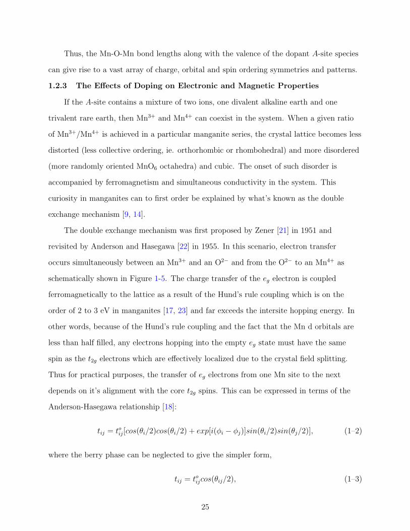
The double exchange mechanism was first proposed by Zener [21] in 1951 and
revisited by Anderson and Hasegawa [22] in 1955. In this scenario, electron transfer
occurs simultaneously between an Mn3+ and an O2− and from the O2− to an Mn4+ as
schematically shown in Figure 1-5. The charge transfer of the eg electron is coupled
ferromagnetically to the lattice as a result of the Hund’s rule coupling which is on the
order of 2 to 3 eV in manganites [17, 23] and far exceeds the intersite hopping energy. In
other words, because of the Hund’s rule coupling and the fact that the Mn d orbitals are
less than half filled, any electrons hopping into the empty eg state must have the same
spin as the t2g electrons which are effectively localized due to the crystal field splitting.
Thus for practical purposes, the transfer of eg electrons from one Mn site to the next
depends on it’s alignment with the core t2g spins. This can be expressed in terms of the
Anderson-Hasegawa relationship [18]:
tij = toij[cos(θi/2)cos(θi/2) + exp[i(φi − φj)]sin(θi/2)sin(θj/2)], (1–2)
where the berry phase can be neglected to give the simpler form,
tij = toijcos(θij/2), (1–3)
25

Figure 1-5. An illustration of the double exchange mechanism in manganites. Here twoMn atoms are shown connected with an O atom (bottom) and the Mn eg
orbitals are hybridized with the O 2p orbitals. The degree of deviation from180 of the angle θ in the Mn-O-Mn bond determines the degree of chargelocalization vs. hybridization present in the compound. The red arrowsrepresent eg electron spins. The schematic diagram of the Mn energy levelswith the core spins and the eg spins interacting with the O 2p states is alsoshown∗ (top). ∗Note: Schematic reproduced from a public domain imageavailable freely on Wikipedia, the free web-based encyclopedia, and is agood [14, 17] schematic description of the mechanism.
which dictates that the absolute magnitude of the electron hopping between two Mn
neighboring sites depends on the relative angle, θij, between their core spins. Thus
ferromagnetically aligned core spins give rise to an increased conductivity in the sample,
qualitatively explaining the CMR effect to first order: Just above the ferromagnetic
ordering temperature (TC), an applied magnetic field ferromagnetically aligns the core t2g
spins, drastically increasing the hopping amplitude given in Equations 1–2 and 1–3.
26

The double exchange mechanism however only provides a very qualitative explanation
of the observed behavior in the manganites, which in actuality is further complicated by
electron-lattice (polaronic) interactions, antiferromagnetic superexchange interactions
between the t2g spins, intersite exchange interactions between the eg orbitals (orbital
ordering) and inter and intra-site Coulomb repulsion between the interacting eg electrons [17,
20].
It is possible in certain manganite stoichiometries to have ferromagnetism but no
conducting state, or localized, ferromagnetically aligned t2g electrons (i.e. a ferromagnetic
insulator), though this is not completely understood. In the ferromagnetic metallic state
however, the manganites are expected to be half metallic (fully spin-polarized) given the
double exchange mechanism and strong Hund’s rule coupling. Recent measurements
have confirmed this speculation in (La,Sr)MnO3 which was found to be over 90%
spin polarized [24]. Magnetization measurements reveal that saturation magnetization
(3.8 µB/Mn) is achieved in the ferromagnetic metallic state [25].
1.2.4 Transport Mechanisms at High and Low Temperatures in DopedManganites
In many of the doped manganites, transport properties at (higher) temperatures [1,
9, 26] before the onset of ferromagnetism are well described within the small (Holstein)
polaron hopping model. This is particularly true near room temperature for the parent
compounds of the manganite discussed in this work, namely Pr0.7Ca0.3MnO3 and
La0.7Ca0.3MnO3. A small polaron is the J-T lattice distortion accompanying a charge
carrier within the crystal. The lattice distortion surrounding the carrier is essentially a
quantum well which ‘self-traps’ the carrier. A large polaron on the other hand, embodies
a weak coupling between the surrounding lattice and carrier. As discussed earlier, the
octahedra containing the eg electrons can lower their energy via a J-T distortion. Thus,
in a mixed valence system where both the cubic octahetra and J-T distorted octahedra
co-exist, the carrier hops to the next site each time the lattice of the neighboring site
27

acquires the necessary (J-T) lattice distortion via thermal fluctuations. The electrical
conductivity is thus activated, since a certain energy is required to obtain the J-T lattice
distortion and is well described by
σ(T ) ∝ T−1exp(−Ep/kBT ). (1–4)
As the temperature is cooled, the undoped manganites (singly occupied A-site) order
into the exotic structural, charge and orbitally ordered phases as briefly introduced in
Section 1.2.2. The samples thus remain insulators down to low temperatures. Doped
manganites with doping levels below those required for electrical conduction exhibit
similar ordering, though often, as in the case of Pr0.7Ca0.3MnO3 there is coexistence in
the sample of ordered phases and paramagnetic disordered insulating phases and the
conductivity is activated, being governed by Equation 1–4. The onset of an insulator to
metal transition upon cooling can be controlled not only by the dopant concentration,
but also the dopant ionic radius. It was found that if the nominal dopant concentration
and average valence were kept constant, reducing the A-site ionic radius also reduces the
transition temperature, since J-T type distortions become energetically favorable [13, 27].
In the doped manganites, at optimal doping levels, the manganites become ferromagetic
and metallic upon lowering temperature. Transport in this temperature range is governed
by the double exchange mechanism. However, the discrepancy between the conductivity
values calculated from double exchange and the measured values suggests that lattice
distortions play a role even in the ferromagnetic metallic state. The effect of such
electron-phonon coupling would be a pronounced temperature dependance of the measured
resistivity, and though observed experimentally, it has not been resolved in the literature
satisfactorily [13, 27]. In Section 1.3 below, the importance of these effects in terms of the
(La,Pr,Ca)MnO6 phase diagram will be introduced.
28

1.2.5 The General Hamiltonian for the Strongly Correlated Manganites
The many competing magnetic, electronic and structural interactions simultaneously
at play in the manganites can be described by the following effective Hamiltonian [18]:
H = HHop + HHunds + HSc + HJT + HB + HU . (1–5)
Here the first two terms describe the essential physics of the double-exchange
mechanism, with the first term describing the ability of the electron to hop from site
to site in the Bravais lattice,
HHop = −2t0
∫d3p
(2π)2
∑Ψ+
p,α, (1–6)
where Ψ+p,α is a two component spinor which accounts for creation and annihilation of
electrons of spin α in momentum space (p). The second term embodies spin dependent
electron hopping between adjacent Mn sites and the double exchange mechanism. In
this case, the eg electron on site i is constrained by the strong Hund’s coupling, which is
estimated to be about 3 eV, to have spin parallel to the core t2g spin:
HHunds = JH
∑~Sci∗d+
iaα ~σαβdiaβ. (1–7)
Here JH is the ferromagnetic (or Hund’s) coupling constant. If JHSc is large enough,
then an electron hopping from site i to j goes from having spin parallel to ~Sci and to ~Scj.
HHunds can essentially be expressed in terms of the hopping amplitude given by Equations
1–2 and 1–3 (see for example [14, 18]).
The next term of Equation 1–5 describes the core spin interactions, i.e. the
antiferromagnetic superexchange interaction:
HSc = JAF
∑~Sci
~Scj. (1–8)
The core spins in this case are represented by ~Scj with i and j representing different lattice
sites.
29
The next two terms of Equation 1–5 describe the electron-lattice interactions, with
HB being the breathing mode given by:
HB = gB
∑d+
iaαdiaαQ0, (1–9)
where Q0 is the breathing mode amplitude, while d+iaα and diaα are the creation and
anhilation operators for electrons of spin α on orbital a on site i, as combined in the
two-component momentum space spinor of Equation 1–6. The second electron-lattice
interaction, the Jahn-Teller distortion HJT can be expressed as:
HJT = g∑
d+iaα ~τabdiaα
~QJT,i, (1–10)
where a and b are two different lattice sites, while g| ~QJT | gives the amplitude of the
splitting between two degenerate eg levels and the direction of ~QJT specifies the particular
linear combinations of eg states which vary in energy due to the distortion.
Finally, the last term, HU describes the Coulomb repulsion between the eg electrons:
HU = U∑
d+iaαdiaα(d+
iaαdiaα − 1), (1–11)
where U is defined as the energy difference between a configuration in which site i has zero
while j has 2eg electrons and a configuration in which each site has one eg electron.
The Hamiltonian given in Equation 1–5 can be solved numerically and analytically
depending on the amount of simplification and types of assumptions used for each of the
components shown above.
1.3 Basic Characteristics of (La,Pr,Ca)Mn)O3
The work described in the following chapters is primarily concerned with the
nanoscale magnetic and electronic properties of the doubly doped manganite, (La,Pr,Ca)MnO3.
The specific stoichiometry of interest is (La1−xPrx)1−yCayMnO3 with x = 0.5 and y =
0.33, and is essentially an equal mixture of two parent compounds: La1−yCayMnO3 and
Pr1−yCayMnO3. To understand the properties of (La,Pr,Ca)MnO3, which is a random
30

(incommensurate) mixture of the two parent compounds, it is necessary to review the
basic properties of each compound for y = 0.33.
1.3.1 Properties and Characteristics of (La,Ca)MnO3
The two end compounds of La1−yCayMnO3 (LCMO), as discussed in Section 1.2.2,
are the Mn3+ manganite LaMnO3 and the Mn4+ manganite CaMnO3. Since both Ca
and La have similar ionic radius size, mixing the two species (or interchanging some
of the La in LaMnO3 with Ca ions) results in mobile charge carriers (hole doping) and
mixed valency rather than induced distortions. It should be noted that a slight distortion
will exist because of the different ionic sizes of an Mn3+ vs. Mn4+, and the very slight
mismatch between the Ca and La radii. Such distortions give rise to a very diverse range
of charge, orbital and spin ordering as a function of La:Ca ratio and temperature.
When the LaMnO3 parent end compound is doped with Ca substitutions, the various
structural, charge and orbital ordered phases undergo a phase transition at critical dopant
concentrations. (Quite curiously, the transition temperatures for the phases are maximized
at dopant concentrations that are multiples of 1/8 [13]). For instance, for small dopant
concentrations (Ca < 5%), LCMO is a paramagnetic insulator at higher temperatures and
undergoes a transition to a canted antiferromagnetic state. For Ca substitutions between
5% and 20%, LCMO exhibits an insulating ferromagnetic state and a charge ordered
state at low temperatures. At Ca concentrations of 20% to 50%, LCMO transitions to a
ferromagnetic metallic state at low temperatures. Higher concentrations result in charge
ordered, antiferromagnetic and canted antiferromagnetic states at low temperatures [13].
The stoichiometry of interest for this work is La1−yCayMnO3 with y = 0.33 (i.e. 33% Ca
concentration), where the compound is a paramagnetic insulator at room temperature
and undergoes an insulator to metal transition to a ferromagnetic metallic state at about
240 K.
LCMO retains a pseudo cubic (slightly orthorhombic, very nearly cubic) ordering
between the MnO6 octahera for all doping (y) and temperature ranges. Thus the
31

insulator-metal transition without an accompanying structural change is considered
second order in nature.
1.3.2 Properties and Characteristics of (Pr,Ca)MnO3
Unlike LCMO, in Pr1−yCayMnO3 (PCMO) the Pr and Ca ions have a considerably
different ionic radius [13, 14]. Hence, in addition to a change in valence with increasing Ca
substituion of Pr in PrMnO3, there are structural distortions with increasing Mn-O-Mn
bond angles and a reduced tolerance factor, f (see Equation 1–1). With increasing Pr
concentration, the structure becomes increasingly orthorhombic, resulting in a reduced one
electron bandwidth, i.e. reduced double exchange charge transfer.
Because of the high level of structural distortions, PCMO is insulating throughout
the entire doping range (all y) and at all temperatures. However, with changing y, there
is a change in phase characterized by different orbital, spin and charge ordering. The
doped charges in PCMO (i.e. Mn3+ sites with an eg electron) and the Mn4+ sites order
in a sublattice (charge ordering) with the eg occupation being staggered or arranged on
a different (sometimes the same) sublattice (orbital ordering). This charge and orbitally
ordered state is most stable with a reduction of the tolerance factor and when the carrier
concentration coincides with a rational number of periodicity of the crystal lattice [27].
The end compound PrMnO3 is a paramagnetic insulator at room temperature with a
transition to an antiferromagnetic spin-canted insulating state near 100 K. At a nominal
concentration of 15% Ca, the system instead transitions to a ferromagnetic insulating
state near 100 K to 150 K, depending on the hole concentration. Ca concentrations
of 30% to 40% result in three transition temperatures. First there is a transition
from a paramagnetic insulating state to a charge ordered insulating state, followed
by antiferromagnetic ordering and finally a transition to a canted antiferromagnetic
insulator at low temperatures. The increase in hole doping via Ca concentration enhances
the tendency towards ferromagnetism, thus resulting in the canted antiferromagnetic
insulating behavior at low temperatures for these concentrations. However, the tendency
32
towards ferromagnetic coupling with increased hole doping is offset by the increased
distortions (the Ca ion distorts the lattice). Thus the canted state only persists between y
= 0.3 to 0.4, above which the antiferromagnetic charge ordered insulating state persists to
low temperatures [27].
Although PCMO remains insulating at all doping levels and temperatures, an
insulator to metal transition can be induced with an applied magnetic field. This is
often referred to a ‘melting’ of the charge ordered phase: The ferromagnetic alignment
of core-spins with an applied magnetic field also aligns the eg spins via the Hund’s
rule coupling, and thus aids carrier mobility via the double exchange interaction (see
Equations 1–2 and 1–3). Thermodynamically, the applied magnetic field reduces the
potential barrier for the system to become conducting by aligning the core spins and
enabling double exchange. Thus, the higher the temperature, the lower the field required
for the transition since thermal energy can assist in overcoming the potential barrier
(thermally induced lattice fluctuations) for melting the charge ordered phase. It should
be noted that unlike the temperature induced insulator to metal transition in LCMO, the
field induced transition in PCMO is a first order transition accompanied by a change in
lattice parameters originating from the field induced destruction of the orbitally ordered
state [8, 14].
The stoichiometry of interest for this work is Pr1−yCayMnO3 with y = 0.33, where
the compound is a paramagnetic insulator at room temperature and undergoes a charge
ordering transition near 240 K with the spins ordering antiferromagnetically below
150 K. Below about 80 K, the antiferromagnetic state becomes canted and weakly
coupled such that it is very nearly ferromagnetic. In fact, the canted state is metastable
since application of a magnetic field irreversibly drives the system into a ferromagnetic
state [13, 14].
33

1.3.3 Properties and Characteristics of (La,Pr,Ca)MnO3
The properties of (La,Pr,Ca)MnO3 (or LPCMO) can best be understood by
considering the two parent compounds discussed in Sections 1.3.1 and 1.3.2 above. An
approximate phase diagram adapted from the LCMO and PCMO diagrams [13, 27]
for LPCMO is shown in Figure 1-6. (La1−xPrx)1−yCayMnO3 with x =0.5 and y = 0.33
exhibits properties inherent to both LCMO and PCMO with decreasing temperature.
There is a competition between the ferromagnetic tendencies of LCMO and the charge and
orbitally ordered tendency of PCMO resulting in an interplay of both states [14, 27, 28].
For some temperatures, both the ferromagnetic metallic state and the charge ordered
insulating state are energetically favorable and thus they coexist on the micrometer scale.
This phenomenon is known as phase separation. Contrary to intuition, the phase separated
regions do not appear to be pinned within the lattice, since the incommensurate mixture
may be expected to contain LCMO or PCMO rich sites. Instead, each cooling run exhibits
a different spatial occupation of each phase [10]
One way to understand the properties of LPCMO is by considering studies of
chemical pressure in the parent compound LCMO [13]. As discussed in Section 1.3.1, since
La and Ca have similar ionic radii, the effects of a mixed concentration is simply a change
in the average valence of the compound, i.e. a mixture of vacant and occupied single eg
orbitals on the Mn sites. The Mn-O-Mn bond angle in this compound remains close to
180 and the compound is ferromagnetic metallic for temperatures below about 240 K for
the y = 0.33 doping concentration. The Mn-O-Mn bond angle can be reduced below the
optimal value of 180 by applying chemical pressure to LCMO. In this case, doping the
La site with Pr will change the effective tolerance factor of the system without changing
the average valence or eg carrier concentration. As the LCMO becomes increasingly
distorted with Pr ions (increasing x in (La1−xPrx)0.67Ca0.33MnO3), the insulator metal
transition temperature decreases and the transition becomes increasingly hysteretic
and first order. There is an increasing tendency towards charge localization and charge
34

Figure 1-6. The approximate (La,Pr,Ca)MnO3 phase diagram showing the end compounds(La,Ca)MnO3 and (Pr,Ca)MnO3 phase diagrams. The red line denotes the x =0.33 Ca doping concentration. Although samples for y = 0.4 to 0.6 werestudied, the main results described in this work are for y = 0.5 as highlightedby the grey box. Illustration provided courtesy of Amlan Biswas.
ordering since as previously discussed, PCMO undergoes a charge ordering transition
around the same temperature as the ferromagnetic transition for LCMO (about 240 K).
Near the charge ordering temperature, in LPCMO, there is a martensitic type transition
to the charge ordered(and thus structurally distorted) state in portions of the sample while
the remaining regions maintain a pseudo-cubic structure [29]. The pseudo cubic state
is hypothesized to be paramagnetic, and sometimes referred to as the charge-disordered
insulating state (no clear charge or orbital ordering sublattice) [29–31]. Neutron diffraction
measurements suggest the presence of charge ordered nano-clusters in the paramagnetic
background coexisting with lattice polarons [14]. It is the charge disordered insulating
state that undergoes a first order insulator to ferromagnetic metallic transition at low
35

temperatures. The charge and orbitally ordered states remain insulating down to low
temperatures such that the sample is phase separated into metallic and insulating regions.
In essence, the suppression of long range Coulomb interactions play an inherent role in
stabilizing the phase separated state [14].
The Pr doped LCMO or LPCMO remains ferromagnetic at low temperatures for x <
0.7, above which, the canted antiferromagnetic insulating state of PCMO is prevalent.
For x < 0.7 the low temperature ferromagnetic state in LPCMO can be understood
by noting that below about 80 K, the canted insulating state in PCMO is metastable
and very nearly ferromagnetic. Thus, when analyzed from the perspective of La doped
PCMO, increasing La content increases the competition between antiferromagnetism
and ferromagnetism eventually tipping the scale in favor of ferromagnetism when a
high enough La concentration is introduced (or in the LCMO picture, ferromagnetism
increases for small Pr concentrations in LCMO) [8]. This fact demonstrates that both
magnetic field or a reduction in chemical pressure can induce ferromagnetism in PCMO by
changing the effective double exchange hopping integral and reducing the superexchange
antiferromagnetic interactions.
Essentially, for the LPCMO concentration discussed in this work, specifically
(La0.5Pr0.5)0.67Ca0.33MnO3, in bulk form the compound is a paramagnetic insulator at
room temperature [13]. With decreasing temperature, around 240 K, there is a transition
of portions of the sample to a charge ordered state while the other portions remain
insulating, but in the absence of a charge or orbitally ordered sublattice. Below about
100 K, the charge disordered portions of the sample transition to a ferromagnetic metallic
state and there is coexistence of the insulating and metallic regions in the sample. At low
temperatures, the sample is phase separated into charge ordered regions and majority
ferromagnetic regions. A magnetic field as low as 2T can transform the sample into a fully
metallic ferromagnetic state.
36

1.3.4 Substrate Induced Strain in (La,Pr,Ca)MnO3 Thin FIlms
The temperature dependent phase changes in LPCMO can be modified with substrate
induced strain [32]. A compressive or tensile strain in this case acts to reduce or enlarge,
respectively, the lattice constants in the plane of the film while the out of plane lattice
constants are increased or decreased respectively. Figure 1-7 schematically depicts
the effects of substrate induced strain. The effect on LPCMO thin films grown on
orthorhombic NdGaO3 substrates with a (011) orientation is a very slight compressive
mismatch within the plane of the film with an elongation perpendicular to the plane of the
film. NdGaO3 (011) is essentially orthorhombic with calculated in-plane lattice parameters
of 0.3855 nm and 0.3860 nm at room temperature (using unit cell lattice constants of
a = 0.5430 nm, b = 0.5500 nm, c=0.7710 nm [33]). The lattice constant for LPCMO
on average (since it is multiply doped) in the paramagnetic pseudo cubic state at room
temperature is 0.384 nm [34]. Thus at room temperature, the lattice mismatch between
LPCMO and the NdGaO3 substrates is with 0.4% in one direction and 0.6% in the other
in-plane direction. The NdGaO3 substrates hence induce a very slight tensile strain on the
LPCMO thin films, slightly increasing the average Mn-O-Mn bond angle and decreasing
distortions thus enhancing the one electron band width (tendency towards Mn-O orbital
hybridization and double exchange).
The lattice constants are different for the different phases present in LPCMO
(ferromagnetic metallic vs. charge ordered insulating). Thus, as the temperature is
lowered and the LPCMO undergoes phase transitions, the lattice mismatch increases,
affecting the phase changes for very thin (< 100 nm) LPCMO films studied in this work,
which are constrained to the lattice parameters of the substrate. The two main affects of
NdGaO3 (011) substrates on the LPCMO phase transitions are: a) The lack of a hysteretic
feature in the R(T ) data near the charge ordering transition temperature, suggesting
that the charge ordered phase is suppressed due to substrate induced tensile strain which
effectively increases the Mn-O-Mn bond angle in this case. Note that the charge ordered
37
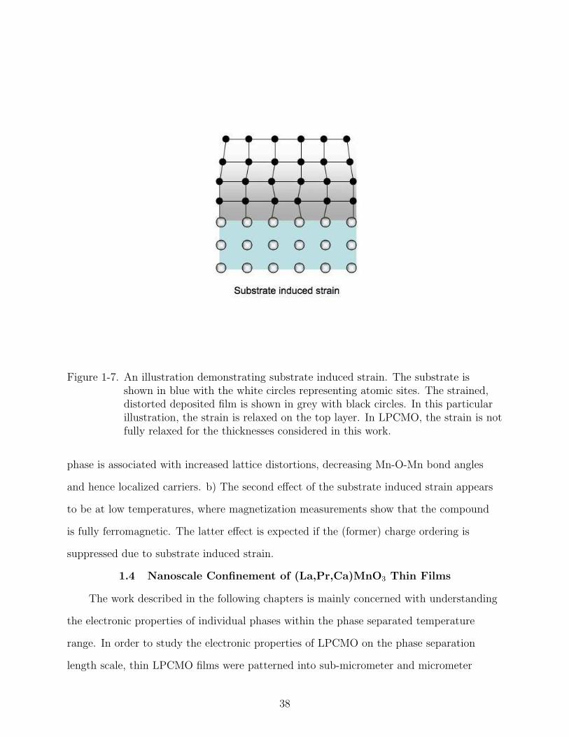
Figure 1-7. An illustration demonstrating substrate induced strain. The substrate isshown in blue with the white circles representing atomic sites. The strained,distorted deposited film is shown in grey with black circles. In this particularillustration, the strain is relaxed on the top layer. In LPCMO, the strain is notfully relaxed for the thicknesses considered in this work.
phase is associated with increased lattice distortions, decreasing Mn-O-Mn bond angles
and hence localized carriers. b) The second effect of the substrate induced strain appears
to be at low temperatures, where magnetization measurements show that the compound
is fully ferromagnetic. The latter effect is expected if the (former) charge ordering is
suppressed due to substrate induced strain.
1.4 Nanoscale Confinement of (La,Pr,Ca)MnO3 Thin Films
The work described in the following chapters is mainly concerned with understanding
the electronic properties of individual phases within the phase separated temperature
range. In order to study the electronic properties of LPCMO on the phase separation
length scale, thin LPCMO films were patterned into sub-micrometer and micrometer
38

wide bridges (or wires with contacts pads) as described in Chapter 2. In this manner, as
described in detail in the following chapters, a few insulating and metallic phases appear
across the length of the bridge during the phase separation temperature range.
There are several potential ways in which the properties of LPCMO structures
confined to the nanometer scale may be affected. For instance, surface states differ
from the bulk due to the strong dependence of charge, spin and orbital ordering on the
lattice structure. Dangling and incomplete bonds on the surface can result in drastically
different properties on the surface such as the suppression of double exchange even if the
bulk portions are ferromagnetic metallic [24]. Charge and orbital ordering may also be
suppressed resulting in a disordered state. In nanostructures, the surface to volume ratio
is enhanced and thus surfaces play an important role in determining the properties of the
system. Secondly, long range Coulomb interactions are suppressed in nanostructures. In
the case of bridges, the interactions are suppressed along one axis, possibly modifying
the phase separation tendencies in the sample. The potential consequences of suppressed
long range Coulomb interactions in reduced dimensions in manganites is addressed in
Chapter 4.
The advantage of studying the effects of magnetic and electric fields on transport in
nanoscaled LPCMO structures is clear from the experiments described in Chapters 3, 4
and 5. Measurements on nanostructures make it possible to separately identify each of
the different effects simultaneously at play in the manganites, giving the exotic electronic
transport properties observed in bulk materials. For instance, it is possible to separate
electron tunneling effects across different insulating regions from metallic transport and
compare the effects of the electronic vs. magnetic fields on the insulating regions. The
data hint at the presence of an intrinsic exchange bias between the insulating and metallic
regions within the phase separated temperature range and additionally, the possibility
of Coulomb blockaded metallic droplets within the insulating background at higher
temperatures (see Chapters 3 and 5).
39

1.5 Chapter Summary
A general background of the key concepts involved in understanding the electronic
properties of manganites was reviewed in this chapter. The concepts of crystal-field
and Jahn-Teller splitting help understand the origin of the many different structural
arrangements possible in manganites. The degree of Jahn-Teller type lattice distortions
and the presence of charge carriers in the system can be tuned by the ionic size and
valence charge of the dopant atoms introduced in the various parent compounds such as
CaMnO3 and LaMnO3. The carrier concentration and lattice distortions determine the
charge, spin and orbital ordering present in the system.
The parent compounds of the manganite (La,Pr,Ca)MnO3 discussed in this work
have ground states at low temperatures that are ferromagnetic metallic for (La,Ca)MnO3
and a combination of charge/orbital ordered and canted antiferromagnetic insulating for
(Pr,Ca)MnO3. The incommensurate mixture (La,Pr,Ca)MnO3 is thus an intermediate
compound with metastable states and an intimate interplay between insulating and
metallic behavior, giving rise to the micrometer scale phase separation observed at certain
doping levels.
In this work, a study of the nanoscale electronic properties of phase separation
are presented. Thin (La,Pr,Ca)MnO3 films are patterned into narrow bridge structures
such that one or a few regions of each phase are present allowing a direct electronic
measurement of the properties of each of the two phases.
40
CHAPTER 2SAMPLE FABRICATION AND MEASUREMENT TECHNIQUES
In order to probe the electronic properties of phase separated manganites on the
nanometer scale, a novel nanofabrication technique was developed. The nanofabrication
technique, as described in this chapter, has allowed the measurement of not only the
stability of phase separation on the nanometer length scale but also transport across
individual phase separated regions. Such a measurement was possible by fabricating thin
wires (or bridge structures) with widths less then the phase separation length scale so that
a few discrete phase separated regions were trapped along the length. Additionally, a novel
technique for fabricating manganite capacitors with a unique geometry was employed to
probe anisotropic transport that results from confining film thicknesses to the nanometer
length scales. As discussed in detail in the subsequent chapters of this thesis, using the
former unconventional fabrication techniques several effects unique to this lengh scale were
observed, including (1) tunneling across intrinsic insulating regions separating adjacent
ferromagnetic metallic regions, (2) evidence of a new type of highly resistive magnetic
domain wall, (3) discrete colossal electric field induced resistance steps and (4) inherent
transport anisotropies linked to anisotropies in crystal structure resulting from substrate
strain. The investigation is however on going and many new phenomenon beyond those
described in this thesis remain to be uncovered. The fabrication techniques presented
below can also be utilized on other phase separated or correlated electron oxide systems to
better understand physics on the nanometer length scales.
In this Chapter, the techniques used to fabricate the manganite nanobridges as well
as the manganite thin film capacitors are discussed in detail. The measurement set-up
for both the ac and dc four terminal resistivity and the three terminal capacitance will
be discussed followed by a description of the Quantum Design PPMS apparatus used for
both temperature and magnetic field dependence. Lastly, magnetization measurements
41

A B
Figure 2-1. A. Shows a schematic of the pulsed laser deposition (PLD) system while, B.shows a photograph of the PLD main chamber (circular, metallic, withmultiple ‘feedthru arms’) with the laser unit (orange) immediately behind.
using the Quantum Design MPMS SQUID apparatus will be discussed followed by data
acquisition techniques.
2.1 (La,Pr,Ca)MnO3 Thin Film Deposition
The (La0.5Pr0.5)0.67Ca0.33MnO3 or LPCMO thin films were deposited on NdGaO3
(110) or NGO substrates with a technique known as pulsed laser deposition (PLD), using
a system built by Dr. Amlan Biswas. The initial films measured for the work presented in
the following Chapters were deposited and provided by Dr. Tara Dhakal, a graduate from
the Biswas lab. All subsequent films were deposited by myself following training on usage
of the PLD system provided by Dr. Biswas.
The PLD process comprises a laser, a target material and a target substrate as
shown in Figure 2-1. The target material is generally a bulk pellet of the desired material,
sometimes of the desired composition and sometimes of a slightly different composition
which is later tuned by changing the chamber pressure and/or temperature of the
substrate. The substrate is a thin (in this case 0.5mm thick) single crystal material which
is nearly lattice matched to the desired deposition material in order to avoid strain and
42

attain epitaxial (lattice matched) thin film growth. This way, it is possible to measure the
properties of crystalline materials in thin film form by avoiding the tremendous challenges
of obtaining a free standing ultra-thin single crystalline film. Lastly, the laser—here a
248 nm eximer laser—is focused onto the target and pulsed on and off. Each pulse ablates
material from the target creating a visible plume of the desired material in elemental form,
as shown in Figure 2-2.
Figure 2-2. This photograph depicts a plume (white) created by the laser striking thetarget material on the right. Note that the tip of the outer edge of the plumevery nearly coincides with the heater (red/orange, 820C) where the substrateis mounted.
The substrate position is optimized to coincide with the tip of the plume. In this way,
each laser pulse results in material being deposited on the film—generally less than one
monolayer per pulse. The substrate temperature is optimized to ensure crystalline growth.
In other words, the atoms must have enough thermal energy once on the surface to move
around and find the position of lowest energy (potential well), thus allowing atomically flat
layer by layer deposition. The ambient pressure determines not only the plume size, but
if the material being deposited is an oxide, it also determines the oxygen content. Hence,
in this case, the oxygen pressure also required a considerable amount of fine tuning by Dr.
Dhakal [25].
The optimum parameters for LPCMO growth on NGO were determined through
extensive trial and error [25]: Substrates were mounted onto a substrate heater which
43

was heated to a temperature of 820 C at a rate of 20 C/min partly in a vaccum with a
pressure of 10−6 Torr (for approximately the first 600 C) and partly in a partial pressure
of O2. A partial pressure of oxygen was stabilized at 450 mTorr prior to growth. The
target was pre-ablated for 5 minutes at a rate of 10 Hz to remove impurities and the
damaged top layers. The optimum laser energy was found to be 480 mJ. (Note that too
high of a laser energy can result in uneven and non-epitaxial growth. Large granules and
an uneven surface can be seen in this case. Too low of a laser energy results in inadequate
target ablation, inhomogeneous ablation and a smaller plume.) After pre-ablation, the
laser pulse rate was reduced to 5 Hz and the shutter was removed exposing the substrate
to the plume, thus beginning the thin film deposition.
Standard θ-2θ x-ray diffractometry was used to determine the composition and
crystalinity of the samples [25]. The x-ray results were used in combination with transport
and magnetization measurements to determine the quality of the LPCMO thin films [25]
2.2 (La,Pr,Ca)MnO3 Nanobridge Fabrication
After several months of trial and error and several years of subsequent modification,
a recipe to fabricate LPCMO nanobridges was developed. The work was initially carried
out in collaboration with my colleague, fellow Hebard lab student Sinan Selcuk. After
acquaintance and familiarity with the nanofabrication techniques, the process was
subsequently developed by myself and is constantly being modified. Nanofabrication
techniques for metals and semiconductors have been known now for several decades.
Metals conduct, a property which eases electron beam patterning since the bombarded
electrons can easily be shunted to ground instead of becoming trapped on the sample
surface deflecting the incoming electron beam. Further, metals are easy to etch with
known dry and wet etches in a quick and controllable way. Semiconductors, though more
chemically complex than metals, have enjoyed a great deal of research from both industry
and the academic research sector, thus numerous nanofabrication techniques and recipes
exist for fabricating nanostructures from thin films. The manganites on the other hand
44

have a complex chemistry and are ‘robust’ oxides and thus difficult to etch with much
control and further can be quite insulating for the purposes of electron beam patterning
at room temperature. Dry etching of manganites can compromise the crystal composition
because of oxygen depletion. In addition, wet etch recipes are not widely known and much
research is required to develop a controlled wet etch for manganites. The following sections
demonstrate the steps taken to overcome these challenges to successfully pattern and
fabricate thin film manganite nanobridges.
2.2.1 Challenges in Manganite Nanofabrication
The first step in creating bridges from manganite thin films was developing a photo
lithography mask, as described in the next section. A wet etch was subsequently
used to remove the unmasked manganite as described next. The resolution of the
photolithography technique however is approximately 1 µm and is thus not suitable
for making bridges with widths on the order of 100 nm, the desired width range for
fabricating samples which are less than or on the order of the phase separation length
scales.
Electron beam (E-beam) patterning is able to overcome the lower limits presented by
the UV photo lithography technique. As noted earlier however, the challenge of patterning
with the (E-beam) is the relatively low conductivity of LPCMO at room temperature.
Depositing a metal layer on the manganite was not straightforward because both chemical
and dry etch removal techniques resulted in surface damage and thus structural damage
to the manganites and hence altered transport properties. For instance, even if an etch
that does not affect manganites is used to remove the metals, the surface of the manganite
is damaged from oxygen loss to the metal. Though metals such as gold which do not
oxidize easily were utilized, no suitable selective gold etch was found: All etches used for
this study damaged the manganite thin film. Another challenge with E-beam patterning
was the subsequent etching of the exposed regions using wet or dry etches and associated
complications with wall damage to the ultra narrow bridge.
45

2.2.2 Nanopatterning of Substrates
Since the challenges with E-beam patterning were too great, we opted for a technique
known as focused ion beam (FIB) milling. The FIB is essentially a narrow (down to a few
angstroms) beam of charged gallium (Ga) ions, which when aimed at a given surface can
ablate with precision. The beam can be automated and programmed to ablate regions
in whatever shape desired. The beam current and voltage must be optimized for each
material being ablated. Too low of a beam current can result in no ablation and Ga ion
implantation in the target material. Too high of a beam current can result in loss of
precision and again, unacceptable levels of Ga ion implantation through the pattern side
walls.
In direct analogy to an E-beam system, the Ga ion beam requires focusing and
the sample can essentially be ‘viewed’ by bombarding Ga ions (as with electrons for an
electron microscope or photons in an optical microscope). Thus, simply focusing the ion
beam or viewing a sample in this way can result in Ga ion implantation in the desired
sample. The FIB is generally used for fabricating samples for transmission electron
microscopy which are coated with a protective metallic layer, thus Ga ion implantation
is not a major issue. In the thin manganite films used for this work however, it was
found early in the project that Ga ion implantation in the manganites resulted in altered
transport properties and no insulator to metal transition.
To avoid Ga ion implantation directly into manganites, we patterned the NGO
substrates using the FIB. Since NGO is insulating and thus prone to charging problems
from the Ga ion beam, we deposited a 40 nm to 80 nm thick film of transparent
conducting nanotubes (CNT) in collaboration with Dr. A. Rinzler [35]. Since a pristine
and atomically smooth substrate surface is essential for achieving high quality LPCMO
thin films for our experiments, the inert CNT thin films were better suited as a conducting
layer for FIB purposes than conventional metals. Because CNT’s are inert when in contact
with the substrate, the smooth surface of the substrate is preserved. It was found that
46

the deposition of metals as the conducting layer on NGO and subsequent removal using
various wet etches resulted in considerable damage to the substrates, just as it did for
manganites as discussed in Section 2.2.1. Most of the metals readily available in our
laboratory (i.e. Al, Au, Cu) tend to oxidize thereby depleting the oxygen in NGO near
the surface and changing not only the surface chemistry but the crystal structure, and
resulting in undesirable surface roughness. The advantage with CNTs lies in the fact that
they do not deplete NGO surface oxygen and can easily be removed with a low power O2
plasma which was found to not affect the NGO.
Figure 2-3. Two typical scanning electron micrographs of a transparent conducting carbonnanotube thin film covering the NdGaO3 substrate, prior to FIB milling.
Figure 2-3 shows an SEM image of a typical substrate coated with a CNT film prior
to FIB milling. Small rectangular grooves or lines defining the desired bridge width as
shown in Figure 2-4 were milled into the center of the substrate using the Dual Beam -
Focused Ion Beam Strata DB 235 apparatus available at the University of Florida Major
Analytical Instrumentation Center (MAIC), see Figure 2-5. The ‘dual beam’ feature of
the FIB is additionally useful in avoiding Ga ion contamination since it consists of two
beams: the Ga ion beam and an E-beam. Both beams can be focused at the same point
47

A
B C
Figure 2-4. A. Schematic showing rectangular grooves in the NGO substrate etched usingthe FIB. The spacing of the grooves defines the width, d, of the bridge to befabricated between them. B. Shows a scanning electron micrograph (SEM) of acarbon nanotube coated NGO substrate immediately after patterning oftrenches 1 µm deep, 40 nm wide to define the bridge (as opposed to grooves,see end of Section 2.2.3). C. An SEM image showing details of the groovesdepicted in part B. The nanotube thin film is visible.
thus allowing images to be obtained with the minimally invasive E-beam while milling
with the ion beam. The ion beam focusing sequence can be performed at the sample
edge, far away from the desired pattern area and the E-beam can subsequently be used to
define a patterning area, avoiding Ga ion contamination. In this way, the areas that are
not directly being milled will avoid a major influx of Ga ions. The lowest available beam
current settings of 1 pA or 10 pA and a beam voltage of 30 kV was used to minimize Ga
‘side wall’ contamination (i.e. Ga ions with enough momentum and energy implanting
48

into the sample not from above, but laterally through the walls of the milled area). The
pattern is milled to a 0.5 µm depth to avoid connectivity of the film to be deposited along
the pattern side walls, since the deposited manganite film is on the order of 10 nm (a
thickness much less than the depth of the milled regions).
Figure 2-5. The Dual Beam - Focused Ion Beam Strata DB 235 apparatus available at theUniversity of Florida Major Analytical Instrumentation Center (MAIC). Photocourtesy, MAIC.
After successful FIB milling, the sample was removed and placed in an Anatech SCE
600 Asher. An O2 plasma was used at a power of 600 W for 20 mins to remove the CNT
thin film by oxidizing the carbon nanotubes, resulting in CO2 gas. Next, an LPCMO
thin film was deposited on the patterned substrate using the PLD system as depicted in
Figure 2-6.
2.2.3 Nanobridge Formation Using Photolithography and Wet Etching
Once deposition of the manganite on the patterned substrate is complete, the sample
is ready for UV photolithography using equipment available at the University of Florida
Physics Nanofabrication facility. Photolithography is used to isolate the bridge from
the rest of the manganite on the substrate so that the end product is a bridge with two
leads on either side for measurement. This is shown both schematically and in an optical
microscope photograph in Figures 2-7 and 2-9 respectively.
49

Figure 2-6. Schematic showing the etched substrate (grey) before and after LPCMO (red)deposition. The substrate grooves are deep enough to ensure minimal LPCMOdeposition on the side walls, and thus minimal electrical contact between theLPCMO on the substrate and that deposited within the grove. Figure not toscale for clarity.
Figure 2-7. Schematic showing LPCMO (red) deposited on etched substrate (grey) beforeand after the bridge is defined using UV lithography. Figure not to scale forclarity.
Figure 2-8. A schematic (not to scale) depicting the four contact pad UV lithographymask used to isolate and define the bridge prior to wet etching.
50

Next, a 3:1 solution of Shipley S1813 photoresist and thinner was spin coated for
40 sec at 5000 rpm onto the sample using a Laurell spinner. The sample was then baked
on a clean surface hotplate at 115 C for 90 sec. A mask with the pattern shown in
the schematic of Figure 2-8 was developed using the Autocad software package in our
laboratory and printed by Photo Sciences, Inc. As noted previously, the lower limit of
resolution with our UV photolithography system is approximately 1 µm. Thus a mask
with a bridge width of 3 µm was developed. A Karl Suss MA-6 Contact Mask Aligner was
used to align the substrate pattern with the photolithography mask in soft contact mode.
This particular step, given the low resolution on the Mask Aligner microscope, sometimes
involved several hours of tedious and careful alignment. Once aligned, the sample was
exposed for 14 sec and subsequently developed using Microposit MF 319 developer for
10 sec and then rinsed in deionized water. Figure 2-9 shows an optical microscope image
of a successfully aligned and developed bridge structure. Note that in this case, instead of
grooves, 1 µm deep, 40 nm wide trenches were milled with the FIB to define the bridge, as
a time saving measure (narrow trenches take less time than wide rectangular grooves).
The final fabrication step involves etching the exposed, unmasked manganite using
an in-house recipe for a solution prepared from a titration between potassium iodide and
10% hydrochloric acid. Since the solution is unstable and the etch rate varies with the age
of the solution, prior to etching a given sample small strips of manganite films on NGO
are used to determine the exact time of the etch. Etch timings range from 8 sec to over
a minute. Thus precise timing is crucial since one second too long can result in etching
through the narrow bridge in the center.
Once successfully etched, the photoresist mask is removed by sonicating the sample
first in acetone for one minute followed by isopropanol and methanol also for a minute
each followed by nitrogen gas blow drying. An optical image of a completed manganite
bridge is shown in Figure 2-9B.
51
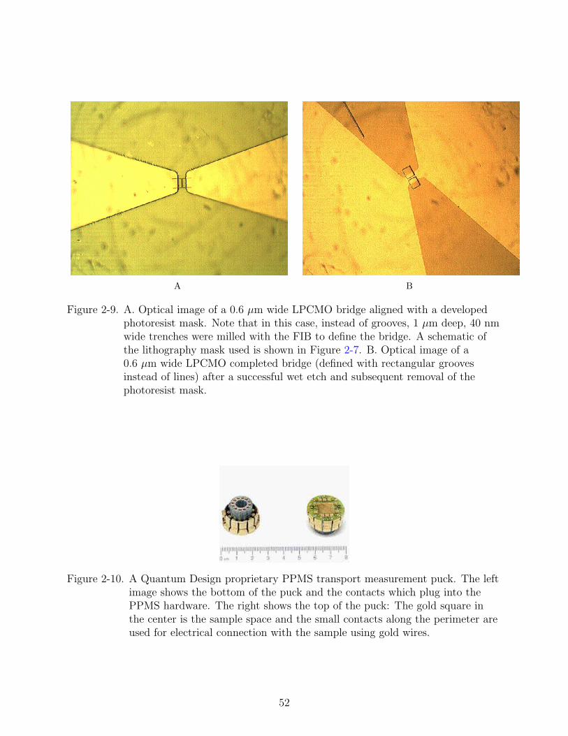
A B
Figure 2-9. A. Optical image of a 0.6 µm wide LPCMO bridge aligned with a developedphotoresist mask. Note that in this case, instead of grooves, 1 µm deep, 40 nmwide trenches were milled with the FIB to define the bridge. A schematic ofthe lithography mask used is shown in Figure 2-7. B. Optical image of a0.6 µm wide LPCMO completed bridge (defined with rectangular groovesinstead of lines) after a successful wet etch and subsequent removal of thephotoresist mask.
Figure 2-10. A Quantum Design proprietary PPMS transport measurement puck. The leftimage shows the bottom of the puck and the contacts which plug into thePPMS hardware. The right shows the top of the puck: The gold square inthe center is the sample space and the small contacts along the perimeter areused for electrical connection with the sample using gold wires.
52

To measure the sample, 0.00125” guage gold wire was attached to each measurement
pad by pressing small cut indium (In) blocks (∼1mm3). Using In solder gold wire is
subsequently attached to gold pads on a puck such as the one pictured in Figure 2-10
which connects through electrical contacts and wiring in our PPMS measurement system
(described in Section 2.5 below) to the measurement instruments.
2.2.4 Back and Top Gating of (La,Pr,Ca)MnO3 bridges
To measure the effects of electric field gating on the transport properties of the
LPCMO nanobridges, metal gates were deposited both on top of the LPCMO wires and
on the back side of the NdGaO3 substrates. For the back gates, the insulating NdGaO3
substrates acted as the gate dielectric, though due to the relatively large dielectric
(substrate) thickness (0.5 mm), large applied voltages (∼ 102 V) were required to achieve
electric fields ∼ 10V/cm, reaching the upper limit of our capability. The top gates which
were separated from the LPCMO bridges via thin film (∼ 10nm) AlOx dielectrics, required
relatively small voltages (∼ 10−5V) to obtain the same fields—though with the realistic
possibility of a dielectric breakdown.
The deposition of the AlOx dielectric thin films is described in Section 2.3.1 below.
The metal electrode deposition for both the top and bottom gating electrodes is described
in Section 2.3.2. A photolithography technique similar to the procedure described in
Section 2.2.3 above was used to define the bottom gate and the top gate such that the
gate was aligned with the bridge with minimal overlap with the measurement leads as
shown schematically in Figure 2-11.
2.3 (La,Pr,Ca)MnO3—AlOx—Metal Capacitor Fabrication
Since NGO, the substrate with the best lattice match to LPCMO is insulating,
measuring the dielectric response of LPCMO thin films is a non-trivial matter. In other
words, if NGO were a conducting substrate, LPCMO could serve as the dielectric layer
with a conducting NGO electrode on one surface and a metal could be deposited on the
other surface of LPCMO, forming a tri-layer capacitor. Utilizing a conducting substrate in
53

Figure 2-11. The schematic above shows the bridge capped with a layer of AlOx followedby a thin metal layer (Au shown) such as Au or Al acting as the gate.
place of NGO will alter the strain and thus the properties of the LPCMO film, thus NGO
is most desirable in order to study the LPCMO in its least strained form. To overcome
this difficulty, a novel capacitance structure where the material under test, LPCMO,
comprised one of the electrodes of an electrode-insulator-electrode capacitor structure as
shown in Figure 2-12, was developed by Dr. Ryan P. Rairigh, a previous members of the
Hebard lab. Following Dr. Rairigh’s graduation, the remaining samples were fabricated
by myself on films deposited by Dr. Tara Dhakal. Note that in contrast, a conventional
capacitor geometry comprises a metal–(material under test)–metal configuration. Through
extensive circuit modeling and analysis of the unconventional capacitor structure, detailed
in Chapter 6, the potential drop parallel to the plane of the film was isolated from the
voltage drop perpendicular to the plane of the film. In this way, it was determined that
the insulator-to-metal phase transition within the plane of the film occurs at a different
temperature than the phase transition perpendicular to the plane of the film. The phase
54

transition is thus anisotropic, a property that thickness dependence measurements reveal
can be attributed to substrate induced strain.
Figure 2-12. A schematic (not to scale) depicting all the layers of the capacitor structurewith LPCMO as one of the electrodes and a circularly defined Al thin film asthe second electrode.
The LPCMO trilayer capacitor structure comprised of an AlOx dielectric layer topped
with a metal electrode. The AlOx was deposited using RF magnetron sputtering and a
metal evaporation chamber was used to deposit an Al electrode as described in Sections
2.3.1 and 2.3.2 respectively below.
2.3.1 RF Magnetron Sputtering of High Quality AlOx Dielectric Thin Films
In an rf or dc sputter deposition system, ions from an inert gas are accelerated to
remove (or sputter) material from a target such that constituents of the target material
will land on the substrate. A high voltage or strong electric field is applied between the
target and a ground shield which ionizes the inert gas and accelerates the ions towards
the target material which is bombarded and ablated, hence ‘sputtered’. The target
material for this experiment was Al2O3. Electrons from the ionized gas molecules further
bombard other gas molecules ionizing them in turn, creating a domino effect which results
in a visible plasma. Permanent magnets are used to confine the plasma to the region
55

surrounding the target material. The sputtered constituents of the target material are
then deposited on a substrate.
Figure 2-13. A schematic of the AlOx deposition system, Hamedon system described inthe text is shown and the parts labeled.
For metals, a dc voltage is generally utilized since the conducting target provides
a shunt to ground for the accumulated charge from the bombarding ions. Insulating
materials however do not provide a conducting path to ground and quickly become ionized
deflecting further ion bombardment and thus hinder sputtering. In this case an ac driving
voltage (13.56 MHz, radio frequence–rf) is used. A schematic of our home-built deposition
chamber nicknamed Hamedon is shown in Figure 2-13.
After pulsed laser deposition (Section 2.1), the high quality LPCMO films with a
clean surface were loaded in Hamedon via a load-lock. The system was evacuated using
56

a Cryo-Torr 8 cryogenic pump to a base pressure of ∼ 10−9 Torr. A 30 mTorr pressure
of Ar gas was introduced prior to deposition and an Advanced Energy RFX 600 power
supply and ATX 600 tuning circuit system was used to generate an rf plasma. An Inficon
crystal monitor placed in close proximity to the substrate was used to monitor deposition
thickness. For the purposes of this experiment a 20 nm thick AlOx film was deposited on
the LPCMO thin films.
2.3.2 Thermal Evaporation of Metal Thin Films
After AlOx deposition, the samples were immediately loaded into our in-house
home-built thermal evaporation chamber in order to minimize surface contaminants. The
samples were masked with a metal mask defining top electrodes in the shape of circles
with a 1.5 mm diameter as shown in Figure 2-14.
Figure 2-14. This optical image shows a metal capacitor top electrode (circular) with twogold wire leads attached using silver paint. Numerous reflections in the imagemay divert the eye, although the circular electrode is clearly defined.
Thermal evaporation is a basic metal deposition technique involving the use of a
small tungsten (W) heating element or filament (see Figure 2-15) which holds the desired
metal, in this case Al. When a high current is applied across the heating element, joule
57

heating causes the Al metal to melt and evaporate. The evaporated material lands on the
substrate and the thickness is again monitored using an in-situ Inficon crystal monitor.
The deposited metal thin film properties are optimized by controlling the system base
pressure and deposition rate.
Figure 2-15. Tungsten thermal evaporation boat used for depositing Al top electrodes.Boats of other shapes and sizes were used for other metals such as Au, Ag,Cu, etc.
For the purposes of this experiment, an Al film of 60 nm thickness was thermally
evaporated onto the LPCMO–AlOx structure at a rate of 0.6 nm/sec achieved using
currents of 30 A to 40 A across the tungsten boat, with a base pressure on the order of
∼ 10−7 Torr. Contacts to the metal top electrodes were made using 0.00125” guage gold
wire. Microtipped tweezers were used to bend the wire into a loop (∼ 10 µm diameter)
on one end and dipped in silver paint and quickly removed. With a microscopic drop of
silver paint suspended on the wire loop, the wire was manually placed on the top electrode
so that the paint was confined to the top electrode. After the paint solvents dried, the
gold wire was bonded to the Al with a layer of silver particles. Figure 2-14 shows two wire
loops attached with paint to the top of a 1.5 mm diameter capacitor top electrode.
2.4 Summary of Samples
This section provides a concise table (above) of all manganite samples discussed in
this work. Note that numerous other samples, especially in the case of narrow bridges,
were measure and found to have qualitatively similar properties. However, after initial
measurements performed on all samples (such as R(T ) and R(H) as described below),
58

Table 2-1. This sample summary table only lists the samples for which data is shown inthe subsequent chapters (labeled in the last column). The column labeled‘Type’ identifies each sample as either an unpatterned thin film (film) or apatterned bridge (bridge). Since the 100 µm scale is much large than the phaseseparation scale, sample S2a is considered a thin film. S2b and S2c have beenconsecutively patterned into increasingly narrower bridges from the same initialsample: S2a.
Sample Type In-plane dimensions Film thickness ChaptersS1 bridge 3 µm x 10 µm 30 nm 3S2a film 100 µm x 3 mm 30 nm 4S2b bridge 2.5 µm x 8.0 µm 30 nm 4S2c bridge 0.6 µm x 8.0 µm 30 nm 3, 4, 5S3 bridge 2.5 µm x 8.0 µm 10 nm 4S4 bridge 0.4 µm x 4.5 µm 30 nm 5S5 film 5.0 cm x 5.0 cm 60 nm 6S6 film 5.0 cm x 5.0 cm 30 nm 6S7 film 5.0 cm x 5.0 cm 60 nm 6S8 film 5.0 cm x 5.0 cm 90 nm 6
the detailed measurements were carried out on only a few typical samples (as those
listed here) due to practical issues such as time constraints and available resources. A
quantitative average of properties such as the magnetoresistance cannot be measured for
the bridge samples, since each sample differs from the others quantitatively, though all
possess the same qualitative transport features and properties. This discrepancy is most
likely due to inhomogeneous chemistry of the LPCMO thin films within the narrow bridge.
2.5 Transport Measurements
The experiments described in the remaining chapters consist of three basic measurement
techniques. For the high resistance measurements a typical four terminal resistance setup
was used and in most cases low currents were applied while measuring the voltage output
as described in Section 2.5.1 below. In Section 2.2.4 details of the basic electric field
gating setup are presented and Section 2.5.3 provides a description of the three terminal
capacitance setup. All dc transport measurements were carried out by myself while
the capacitance measurements were carried out in collaboration with fellow Hebard lab
members, Dr. Rairigh, Sef Tongay and Patrick Mickel. While the manganite colossal
59

magnetocapcitance work was pioneered by Dr. Rairigh, the latter two lab members were
trained by myself for future capacitance work.
2.5.1 Basic Resistance Measurement Circuit
Figure 2-16. Four contact resistance measurement circuit diagram showing all instrumentsutilized.
Though the measurement of the manganite bridges was essentially two terminal, to
minimize the contact resistance, the four terminal measurement set up was utilized. This
measurement configuration is essentially two terminal because the two leads (for voltage
and current) at either end of the bridge are shorted via the macroscopic leads. Since most
of the samples measured had resistances on the order of 106 Ω to 109 Ω, in most cases
we supplied current and measured voltage. Current in the range 10−6 A to 10−12 A was
applied using a Keithley 220 current source across the current leads labeled in Figure 2-16.
60

The voltage was simultaneously measured across the voltage leads labeled in Figure 2-16
using a Keithley 182 or the newer Keithley 2182a Nanovoltmeter. Often, the current
supply and voltmeter were substituted with the Keithley 236 Source Measure Unit which
can simultaneously supply and measure both voltage and current. Measurements that
involved sourcing voltage and measuring current were often carried out with the Keithley
236.
Figure 2-17. Two terminal source-voltage, measure-current circuit diagram showing allinstruments utilized. The sample resistance is much greater than the 10 kΩprotection resistor shown. The protection resistor served as a current limiterfor the sensitive SRS 70 current preamplifier in the event of an unexpectedcurrent increase across the manganite bridge. Thus the voltage drop acrossthe protection resistor is negligible compared to the sample being measured.
Though the Keithley 236 sufficed for most voltage sourcing measurements, some
measurements that required more accurate low level current readings when sourcing
a voltage were also made using the Stanford Research Systems (SRS) 570 Current
Preamplifier with excellent noise filtering capabilities, and a Keithley 182 Nanovoltmeter.
61

In this case a voltage was supplied using either a Keithley 2400 Source Measure Unit or a
Keithley 230 Voltage Source. The measurement setup is shown in Figure 2-17. Here the
SRS 570 input is held at virtual ground and the reading is converted to a voltage which
can be read at the voltmeter output and manually converted to a current value using the
scales defined on the preamplifier.
2.5.2 Electric Field Gating
Figure 2-18. Circuit diagram for electric field gating measurement showing all instrumentsutilized.
Figure 2-18 shows a schematic of the measurement setup used to field gate the
manganite bridges. In this case, resistance across the bridge was measured as described
in Section 2.5 above. However, a Keithley 2400 Source Measure Unit was used to supply
the gate voltage with respect to ground as indicated in the figure. Note that to avoid
62

floating voltages and damaging the instruments, all ‘low’ input and output terminals were
connected to a grounding rod available in our laboratory.
2.5.3 Three Terminal Capacitance Measurements
The capacitance bridge used for this experiment was an Andeen Hagerling AH 2700A
with auto-balancing capability. The bridge consists of three main components as shown
in Figure 2-19: The auto balancing bridge circuitry, the precision frequency generator and
the detector.
Figure 2-19. Three terminal capacitance bridge schematic adapted from the AndeenHagerling AH 2700A Users Manual.
The unknown capacitance, Cx (in this case, our sample) is connected as shown in
the Figure 2-19 and either a parallel (shown) or series configuration of a capacitance and
resistance (Rx) is assumed. To determine the capacitance a small amplitude ac signal
is generated by the generator and the bridge runs it’s auto-balancing sequence until the
voltage at the detector is precisely zero. The fact that the ratio of coils at Tap 1 and at
Tap 2 is known and the fact that the voltage at Tap 2 is the same as Leg 4 and that at
Tap 1 is the same as at Leg 3 is used to determine the precise values of the unknown
resistance Rx and capacitance Cx.
63

2.6 Temperature and Magnetic Field Dependence for TransportMeasurements
Transport measurements of the samples as a function of temperature and magnetic
field were conducted in the Quantum Design QD-6000 Physical Properties Measurement
System or PPMS cryostat. A schematic of the cryostat is show in Figure 2-20. The
cryostat consists of a 7 T superconducting manget immersed in liquid He. A liquid
nitrogen (LN2) outer jacket provides a thermal gradient between the He and the ambient
temperature in the laboratory. A vacuum jacket between the He and LN2 as well as
between the LN2 and outer shell of the dewar provides added insulation.
The system provides built in and automated temperature controls with user input
through a software interface, Quantum Design’s Multiview. The PPMS can also be
controlled using Labview software and can easily be interfaced with a computer using the
built-in GPIB connectors as discussed in Section 2.8 below. For cooling, He gas is pumped
into the sample chamber and used to cool the sample down to 4.2 K, and cooling down
to 1.7 K is achieved by filling the ‘cooling annulus’ with liquid He and evaporating. A
feedback system consisting of heaters and thermocouples is used to precisely control the
temperature of the system between 1.7 K and 350 K.
Samples are loaded into the PPMS on a sample puck provided by Quantum Design
and engineered for this particular system, as shown in Figure 2-10. Electrical connectors
on the puck connect internally through the PPMS via co-axial cable and terminate at a
‘break-out’ box with BNC connectors, which enable connectivity with the measurement
instruments.
2.7 Magnetization Measurements
All magnetization measurements were conducted using a Quantum Design Magnetic
Properties Measurement System (MPMS) superconducting quantum interference device
(SQUID). The MPMS measurement SQUID is housed in a dewar similar to the PPMS
system described in Section 2.6 but without the outer LN2 jacket. The sample to be
64

Figure 2-20. Schematic of the Physical Properties Measurement System (PPMS) dewar.Drawing adapted from the Quantum Design QD-6000 Hardware Manual.
measured was inserted and adjusted at the center of a plastic, transparent drinking straw
which was mounted on a sample probe and inserted into the MPMS sample space. Since
the SQUID magnetometer is a differential technique, the relatively faint diamagnetic straw
signal is nearly insignificant since the differential technique renders it a background signal.
The magnetization measurements were carried out in a He purged and evacuated
sample space between 300 K and 10 K. The MPMS system is interfaced via GPIB
65

Figure 2-21. Magnetization measurement of the LPCMO film on the paramagnetic NGOsubstrate. As the overwhelmingly linear overall shape of the curve displays,the paramagnetic substrate signal dominates.
connection to a computer and controlled via the Quantum Design Multiview software
package. Figures 2-21 and 2-22 show magnetization data for a typical 300 A LPCMO
thin film. Figure 2-21 shows the measured signal with the dominant (linear) paramagnetic
NGO substrate signal and Figure 2-22 shows the LPCMO component of the signal after
the linear paramagnetic signal (positive slope—diamagnetic materials have a negative
M(H) slope) is subtracted.
In addition to measuring magnetization of thin films, magnetization measurements
were also performed on 1 µm wide LPCMO stripes patterned on NGO substrates as
shown in Figure 2-23 (fabricated using the photolithography techniques described in
66

Figure 2-22. A linear fit to the paramagnetic signal is subtracted from the signal to givethe LPCMO ferromagnetic contribution as shown here for severaltemperatures.
Section 2.2.3) while simultaneously passing current through the structure. Gold electrodes
were deposited (Section 2.3.2) on the two ends of the stripes as shown on the top right
corner of Figure 2-23 and the sample was mounted on a custom design MPMS sample
holder with electrical wiring for simultaneously performing magnetization measurements
and electrical transport measurements. A typical magnetization curve after removal of the
paramagnetic NGO background signal is shown in Figure 2-24.
2.8 Data Acquisition
Nearly all data were collected using the popular National Instruments Labview
software package, a graphical programming language used to communicate with the PPMS
67
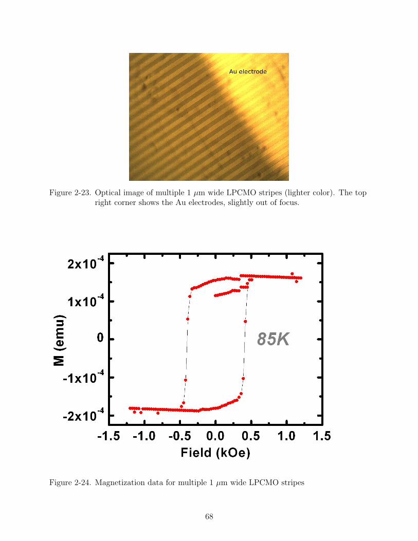
Figure 2-23. Optical image of multiple 1 µm wide LPCMO stripes (lighter color). The topright corner shows the Au electrodes, slightly out of focus.
Figure 2-24. Magnetization data for multiple 1 µm wide LPCMO stripes
68

and all the other instruments mentioned above. The GPIB IEEE-488 protocol is used
to remotely communicate with each instrument which is placed in an electrical screening
room (or Faraday cage) to reduce electrical noise. Fiber optic cables were used to deliver
the signals from the computer to each instrument in the screening room. This greatly
reduced noise in our sensitive high resistance (low current) measurements since computers
and other ambient signals can generate large amplitude noise signals.
The Labview data acquisition programs were in some cases modifications of programs
written by previous lab members but in most cases brand new programs written by
myself. All data were analyzed using a number of software packages including Origin
Lab, Microsoft Excel for less complex analysis, Mathematica and a number of shareware
plotting programs freely available.
2.9 List of Collaborators and Summary of Contributions
The table provided on the following page gives a summary of contributions from all
collaborators mentioned in this chapter. The chapters relevant to the contribution, the
particular task at hand and the exact contribution of each individual is listed according to
chapter and task.
Lastly, it should also be noted that Chapters 3, 4, 6 have partially been reproduced
from work published in scientific journals in accordance with copy right laws. A footnote
in the beginning of each chapter provides the relevant citation and information. In
this respect, in accord with the conventional standards and trends of scientific journal
publications, these chapters and also Chapter 5 which is being adapted for an upcoming
publication, have been presented in plural or collective first person rather than the
objective style of writting employed in Chapters 1, 2 and 3.
69
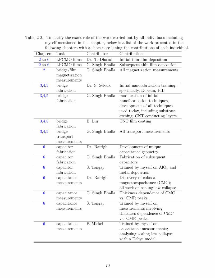
Table 2-2. To clarify the exact role of the work carried out by all individuals includingmyself mentioned in this chapter, below is a list of the work presented in thefollowing chapters with a short note listing the contributions of each individual.
Chapters Task Contributor Contribution
2 to 6 LPCMO films Dr. T. Dhakal Initial thin film deposition2 to 6 LPCMO films G. Singh Bhalla Subsequent thin film deposition
2 bridge/filmmagnetizationmeasurements
G. Singh Bhalla All magnetization measurements
3,4,5 bridgefabrication
Dr. S. Selcuk Initial nanofabrication training,specifically, E-beam, FIB
3,4,5 bridgefabrication
G. Singh Bhalla modification of initialnanofabrication techniques,development of all techniquesused today, including substrateetching, CNT conducting layers
3,4,5 bridgefabrication
B. Liu CNT film coating
3,4,5 bridgetransportmeasurements
G. Singh Bhalla All transport measurements
6 capacitorfabrication
Dr. Rairigh Development of uniquecapacitance geometry
6 capacitorfabrication
G. Singh Bhalla Fabrication of subsequentcapacitors
6 capacitorfabrication
S. Tongay Trained by myself on AlOx andmetal deposition
6 capacitancemeasurements
Dr. Rairigh Discovery of colossalmagnetocapacitance (CMC);all work on scaling law collapse
6 capacitancemeasurements
G. Singh Bhalla Thickness dependence of CMCvs. CMR peaks.
6 capacitancemeasurements
S. Tongay Trained by myself onmeasurements involvingthickness dependence of CMCvs. CMR peaks.
6 capacitancemeasurements
P. Mickel Trained by myself oncapacitance measurements;analysing scaling law collapsewithin Debye model.
70

CHAPTER 3INTRINSIC TUNNELING MAGNETORESISTANCE IN (La,Pr,Ca)MnO3
3.1 Introduction
In this chapter1 we will discuss results from measurements performed on the
(La,Pr,Ca)MnO3 or LPCMO micro and nanometer wide bridges discussed in Chapter 2,
designed to exploit the micrometer scale phase separation into coexisting ferromagnetic
metallic and anti-ferromagnetic insulating (AFI) regions. Fabricating bridges with
widths smaller than the phase separation lengthscale has allowed us to probe the
magnetic properties of individual phase separated regions. First, near the Curie
temperature, a magnetic field induced metal-to-insulator transition among a discrete
number of domains within the narrow bridges gives rise to abrupt and colossal low-field
magnetoresistance steps at well defined switching fields. Further, in the dynamic phase
separation temperature range, our experiments reveal that because of the narrow
width of the bridges, alternating insulating and metallic regions form along the bridge
length. Within this temperature range, we observe the classic signatures of tunneling
magnetoresistance across the naturally occurring intrinsic AFI tunnel barriers separating
adjacent ferromagnetic regions spanning the width of the bridges. In other words, the
bridge essentially resembles a magnetic tunnel junction. The presence of intrinsic tunnel
barriers introduces an alternative approach to fabricating novel nanoscale magnetic tunnel
junctions. The magneto-transport properties of the bridges below the phase separation
temperature range will be discussed in Chapter 4.
3.2 Motivation
Driven in part by the potential for applications in the magnetic storage and memory
industry, the ongoing quest for low-field magnetoresistance (LFMR) has prompted the
1 Contents in this chapter have been submitted for publication to Applied PhysicsLetters under the title “Tunneling Magnetoresistance in (La,Pr,Ca)MnO3 Nanobridges”.
71
exploration of several types of insulating tunnel barriers. To date LFMR studies, which
explore the usage of fields on the order of hundreds of Oersteds (Oe) to switch between
high and low resistance states, have focused on transport across barriers such as grain
boundaries in polycrystalline [36, 37] or bicrystalline [38] films, and across thin film
insulators sandwiched between ferromagnetic metallic (FMM) electrodes in trilayer or
multilayer configurations [39].
Utilizing an altogether different approach, we exploit the micrometer scale intrinsic
phase separation in LPCMO, which, as described in Chapter 1, results from a competition
between the ferromagnetic metallic (FMM) and insulating states with comparable free
energies. When LPCMO thin films are reduced in dimensions to narrow bridges of width
smaller than the individual phase regions, alternating insulating and FMM regions
span the bridge width and the samples exhibit the classical signatures of tunneling
magnetoresistance (TMR). Further, a magnetic field induced insulator-to-metal (IM)
transition among a discrete number of regions gives rise to abrupt and colossal LFMR
steps that are anisotropic with respect to magnetic field orientation.
Recent observations of discrete resistivity steps on such bridges of the mixed phase
manganites Pr0.65(Ca0.75Sr0.25)0.35MnO3 and LPCMO provide evidence of alternating
FMM and insulating regions spanning the full width of the structure [40–42]. However,
spin-polarized tunneling across such intrinsic insulating regions was not considered. Below
we describe the explicit role of spin-polarized currents on magnetotransport in submicron
structures where intrinsic insulating tunnel barriers [43], resulting from phase separation
dominate.
3.3 Review of Transport Across Unpatterned LPCMO Thin Films
The manganite LPCMO as described in Sections 1.3.3 and 1.3.4, is paramagnetic at
room temperature and undergoes a structural transition to a charge ordered antiferromagnetic
insulating (AFI) phase below about 240 K [44, 45]. A typical R(T) curve for our
(La0.5Pr0.5)0.67Ca0.33MnO3 thin films grown on NdGaO3 substrates is shown in Figure 3-1
72

below2 . In bulk single crystals, temperature dependent resistivity measurements
reveal a hysteretic discontinuity at the paramagnetic insulating to charge ordered
insulating transition temperature, which is not seen in our thin films. The lack of such a
discontinuity in thin films does not necessarily undermine the presence of such a transition
(see Chapter 1 but certainly raises questions as to the nature of the transition (first
order vs. second order). Further experimentation beyond the scope of the present work is
needed to confirm this.
0 50 100 150 200 250 300 350102
104
106
108
R(
)
T (K)
Figure 3-1. R(T ) for a typical unpatterned 30 nm thick LPCMO film (sample S1a intable 2-1. Here the blue curve depicts cooling and the red curve, warming.
2 Details of film growth are discussed in Chapter 2.
73
Below the Curie temperature, small FMM islands emerge within the AFI background.
Upon further cooling below the IM transition temperature, TIMO = 105 K, (for unpatterned
films), the FMM regions grow in size, eventually forming connected paths for thin films
grown on NaGdO3 substrates [25]. Due to the dynamic nature (see Section 1.3.3) of
the phase coexistence, below TIMO the FMM and insulating regions are not pinned but
evolve in shape and size with changing temperature, as confirmed by imaging [10, 46]
and time-dependent relaxation measurements of resistivity [44]. Next, below what is
often referred to as the blocking [44] or glass transition [45] temperature TG, (with
TIMO > TG as labeled in Figure 3-2), the sample is predominantly in a single phase
ferromagnetic state [25] characterized by long relaxation time constants. It is within the
phase coexistence temperature range, TIMO > T > TG, that we observe the anisotropic
LFMR and TMR effects across submicrometer wide bridges fabricated from LPCMO thin
films. An approximate phase diagram for LPCMO is shown in Figure 1-6.
3.4 Sample Fabrication and Measurement Techniques
As described in detail in Chapter 2, to fabricate the bridges, we first deposited
single crystalline, epitaxial, 30 nm thick (La0.5Pr0.5)0.67Ca0.33MnO3 (LPCMO) films on
heated (820oC) NdGaO3 (110) substrates using pulsed laser deposition. Next, using
a combination of photolithography and a focused ion beam (FIB), bridges ranging
from 100 nm to 1 µm in width were fabricated. An SEM image of a typical sample is
shown in Figure 2, inset. Pressed indium dots and gold wire were used to make contacts.
Resistance (R) measurements were made by sourcing +/- 1nA DC and measuring voltage.
A magnetic field was applied three consecutive times at each temperature along three
directions Hz, Hx and Hy with respect to the current flow Ix as depicted in Figure 2, and
ramped at 25 Oe/s. The sample identities, as listed in Chapter 2, table 2-1 are noted in
the figure captions.
74

0 50 100 150 200 250100
102
104
106
108
1010
0.6 m x 8.0 m2.5 m x 7.5 m
R(
)
T (K)
TG
TIMO
Hy
Ix, Hx
Hz
TIM
Figure 3-2. Temperature-dependent resistance of sample S1 (see table 2-1, a 2.5 µm widebridge (blue) and S2 (table 2-1) a 0.6 µm wide bridge (green) patterned from30 nm thick LPCMO thin films reveal the evolution of pronounced steplikechanges and the insulator-to-metal transition temperature (see text) as thebridge width becomes comparable to (2.5 µm), and then smaller than (0.6 µm)the micron-size regions of co-existing AFI and FMM phases. A scanningelectron micrograph of a 0.2 µm wide bridge (with the protective polymer andmetal layers still present) taken shortly after the FIB process is shown in theinset together with the orientations of the applied fields: Hx, Hy or Hz
75

3.5 Temperature Dependent Resistivity of LPCMO Bridges
A systematic reduction of bridge width starting at 5.0 µm revealed no significant
changes in R(T) compared to the unpatterned thin films down to 3.0 µm, below which, as
shown in Figure 3-2 (blue curve, compare with Figure 3-1), small steps accompanying the
IM transition begin to appear, since the bridge width is now on the order of the individual
phase separated regions [40]. Significant deviations in the resistivity are observed for
bridges of width less than 0.9 µm, where in most cases the insulator to metal transition
temperature, (TIM = 64 K for the 0.6 µm wide bridge) shifts to a lower value. We
attribute this to dimensionally limited percolation (Figure 3-2, green curve) from three
to two dimensions. A high resistance, temperature independent state begins to appear
below TG = 48 K. Here we discuss data in the range TIMO > T > TG for a 0.6 µm wide
bridge with magnetoresistance properties that are typical of bridges we have fabricated
below 0.9 µm in width. The TMR and colossal LFMR effects occur within the large scale
phase separation temperature range TIMO > T > TG and cease to exist for T < TG, a
temperature range discussed in detail in Section 3-4.
3.6 Magnetoresistance Across the 0.6 µm Wide LPCMO Bridge
Next, we describe the magnetoresistance properties of the 0.6 µm wide bridge.
3.6.1 Magnetoresistance for TIMO > T > TIM
For temperatures above TIMO = 105 K during the cooling cycle, the MR curves are
no different from those observed for unpatterned thin films [25] and are thus not discussed
here. For TIMO > T > TIM with TIM = 64 K however, we observe (Figure 3-3) colossal
(hundred fold) field-induced resistance changes at well-defined anisotropic switching fields.
The temperature range for these large resistance changes coincides with the range where
the maximum colossal magnetoresistive (CMR) effect in our unpatterned films is observed
as shown in Figure 3-4. Here, the high resistance values (≈108 Ω) correspond to limited
conduction through insulating regions which with increasing field are either completely
removed or abruptly shrink to form remnant (lower resistance) tunnel barriers separating
76

-20 0 20
105
106
107
R (
)
70K
-20 0 20
105
106
107
64K
HZ
HY
105
106
10773K
R
()
105
106
107
67K
H (kOe)
Figure 3-3. For temperatures, T > TIM , repeated magnetic field sweeps at the indicatedtemperatures (73 K, 70, 67 K, 64 K) reveal reproducible hysteretictemperature-dependent colossal resistance jumps that are more sensitive toin-plane (Hx, Hy) rather than perpendicular (Hz, arrows with solid heads)fields. Data for sample S1c, table 2-1.
ferromagnetic regions spanning the bridge width. The insulating regions may not be fully
removed for the 2 T fields shown in the figure, since the unpatterned thin-film resistivity
is not achieved unless a field as high as 5 T is applied. Comparison of our results with
the parent compound Pr0.67Ca0.33MnO3 suggests that with decreasing temperature,
there is a reduction in the free energy of the FMM phase, and the regions of insulating
phase undergo a first-order phase transition resulting in a concomitant colossal resistance
drop [47]. In like manner a distribution of such first-order hysteretic transitions over
77

many domains can account for the continuous field induced phase transitions observed in
thin films of LPCMO [25] as shown in Figure 3-4 and in crystals of the parent compound
Pr0.67Ca0.33MnO3 [47].
Figure 3-4. Unpatterned thin film (S1a, table 2-1) R(H) data in rangeTIM > T = 120K > TIMO. The low to high field transitions are smooth whencompared to the bridge data in Figure 3-3. A distribution of the first ordertransitions shown in Figure 3-3 over many domains may account for this.
If the crystalline anisotropy of a thin film is negligible, then the demagnetization
fields arising from shape anisotropy give rise to a greater sensitivity of the magnetization
to in-plane compared to out-of-plane applied fields. In our bridges, magnetoresistance
is affected in the same way; the field-induced changes in the bridge occur more readily
78

for in-plane (Hy, blue curves) easy-axis fields 15, than the out-of-plane fields along Hz.
With decreasing temperature the ferromagnetic regions increasingly fill the available
volume of the 2D film and the corresponding increase of the demagnetizing field results in
increasingly anisotropic phase transitions as seen in Figure 3-3. The magnetic anisotropy
of the CMR effect manifests itself more dramatically in narrow bridges than in thin films,
possibly due to the lack of numerous isotropic planar conduction paths available in films.
Lastly, the sensitivity of the first-order phase transition to thermal fluctuations [47] is
likely to be enhanced near TIM , thus accounting for the unusual asymmetric transitions
observed at the boundary temperature, TIM = 64 K, below which single, irreversible
colossal transitions to a predominantly FMM state occur (T = 57 K).
3.6.2 Magnetoresistance for TIM > T > TG
Below TIM , in the dynamic phase-separated state defined by TIM > T > TG [10,
44, 45], the AFI phase is metastable with respect to applied magnetic fields as the FMM
phase becomes energetically favorable, partially as a result of substrate induced strain [32]
(see also Section 1.3.4). Figure 3-5 illustrates this effect at 57 K. Initially upon increasing
Hy,R(Hy) drops nearly four orders of magnitude and exhibits sharp steps [25, 47], resulting
from an incremental conversion of the insulating phases to FMM. The FMM regions
increase in size and volume, separated by shrinking AFI regions along the bridge length.
Figure 3-5 (inset for 57 K) shows a magnified version of the low-resistance region. Here
we note the distinct formation of low-field peaks (3.5% MR) indicating that the small
amount of insulating phase present between the growing ferromagnetic region acts as
a tunnel barrier. It is useful to compare regions of alternating AFI and FMM phase
along the length of the narrow bridges to microscopic analogs of the insulating and FMM
multilayers. Just as tunneling-magnetoresistance (TMR) is observed in such fabricated
spin-polarized tunnel junctions [39], two resistance states are seen for field sweeps through
zero in each direction: a high resistance state for antiparallel spin alignment (↑↓) and a
low resistance state for parallel alignment (↑↑). As noted in previous theoretical works [48,
79

49], TMR across coexisting AFI and FMM regions in phase separated manganites may
help explain some of the observed transport properties of bulk crystals. For instance, the
small low field ’notches’ in R(H) for unpatterned thin films within the dynamic phase
separated temperature range (see Figure 3-6) may be a manifestation of TMR between
ferromagnetic regions separated by AFI tunnel barriers.
The evolution of TMR across the phase separated regions is better understood by
studying R(Hy) isotherms obtained below TIM . The main panel of Figure 3-7 shows the
evolution of the low-field TMR demonstrating spin-dependent tunnel coupling of adjacent
FMM domains with lowering temperature. For the cooling run shown in the inset of
Figure 3-7, TMR remained at ∼10% for 48 K < T < 52 K. At higher temperatures, the
rise in resistance can occur before crossing Hy=0, which as is evident from the higher
switching field (larger than the measured coercive fields of approximately 500 Oe for
LPCMO thin films), may result from a hysteretic first order phase change. We also note
that the shape and size of the TMR peaks differs for each cooling cycle, as dictated
by a dynamic phase separated state. In fact, during some temperature cycles, we do
not observe any TMR. The asymmetric TMR peaks observed at 51 K (black curve)
and 52 K (blue curve), which were often seen in our measurements, may result from a
unidirectional magnetic anisotropy and exchange bias at the interface between the AFI
and FMM regions, as previously studied for bulk phase separated manganites [50]. Finally,
we note peculiar mangetoresistance steps in Figure 3-7 which are approximately, R =
0.5 kΩ in size. The origin of these steps is not yet clear, though we suspect it is related to
incremental resistance changes associated with the canting of spins at the FMM and AFI
boundaries, or possibly the canting of spins within the AFI tunnel barrier.
3.6.3 Magnetoresistance for TG > T
Below TG, the region in Figure 3-2 corresponding to the high resistance supercooled
state, TMR was not observed since the sample is predominantly FMM [25] upon
application of a field. In this region, we show in the next Chapter that the supercooled
80

Figure 3-5. For temperatures above TB and below TIM , metamagnetic transitions of the0.6 µm wide bridge (Sample S2c in tabel 2-1) terminate in a predominantlylow-resistance ferromagnetic metal (FMM) state that exhibits tunnelingmagnetoresistance (TMR). (a) Metamagnetic transition at 57 K of a ZFCsample showing a pronounced resistance drop at Hz = 6 kOe and subsequententrance into a low-resistance phase that is stable with respect to repeatedfield sweeps between 20 kOe. The inset depicts schematically the coalescenceof FMM (white) regions at the expense of insulating (black) regions withapplied fields or lowering temperatures, with a rectangular overlay depictingthe 0.6 µm bridge. (b) Magnification of the TMR region.
81

Figure 3-6. R(H) for an unpatterned thin film (sample S2a, table2-1) at 50 K showslow-field ‘notches’. This feature may result from a distribution of tunnelingmagnetoresistance across the insulating and metallic regions within the phaseseparated sample.
state consists of thin insulating AFI regions that are stabilized at the ferromagnetic
domain boundary, a phenomenon related to the reduced dimensions of the sample. Upon
application of a field, the insulating stripe domain walls, which act like tunnel junctions
and comprise the remaining AFI phase, are extinguished as spins in neighboring domains
align resulting in sharp resistance drops and a uniform ferromagnetic region spanning the
entire bridge. Thus TMR, which requires stable tunnel junction barriers, is never observed
within this temperature region.
82

Figure 3-7. Waterfall plot of repeated magnetic field sweeps (sample S2c, table2-1) in thetemperature range, TB < T < TIM , showing the temperature-dependentevolution of TMR peaks and their disappearance below TB = 48 K
3.7 Chapter Summary
In summary, temperature dependent magnetoresistance measurements across a narrow
manganite bridge have allowed us to probe the formation and dynamics of the phase
separated regions in LPCMO on the nanometer length scale. At temperatures which
define the onset of large scale phase separation, we have observed abrupt and colossal
low-field resistance changes which are anisotropic with respect to applied field. Further,
within the dynamic phase separated temperature range we have observed evidence of thin
AFI tunnel barriers which span the width of the narrow manganite bridges, separating
adjacent ferromagnetic regions. The observation of reproducible TMR between high
83

(antiparallel) and low (parallel) states confirms spin-polarized tunneling across such
intrinsically-formed tunnel junctions. Pronounced anisotropies and steps in both the CMR
and TMR measurements highlight signatures of various microscopic phenomenon that
occur during phase separation (i.e. exchange bias, shape anisotropy, spin canting) which
can be difficult to clearly identify in bulk sample measurements. From a technological
perspective, control and manipulation of intrinsic tunnel barriers may prove useful for
nanoscale spintronic applications in systems exhibiting similar phase separation.
84

CHAPTER 4EVIDENCE OF UNUSUAL INSULATING DOMAIN WALLS IN (La,Pr,Ca),MnO3
4.1 Introduction
In the previous chapter we showed evidence of spin dependent tunneling across the
intrinsic insulating regions. We now show1 that when the samples are cooled below TG,
the glass transition temperature (see Chapter 2), the intrinsic insulating regions become
thin enough to allow direct electron tunneling in the sub-micrometer wide LPCMO
bridges. Tunneling across these intrinsic tunnel barriers (ITBs) results in metastable,
temperature-independent, high-resistance plateaus over a large range of temperatures.
Upon application of a magnetic field on the order of the LPCMO coercive field, our data
reveal that the tunnel barriers are extinguished resulting in sharp, colossal, low-field
resistance drops. Our magnetoresistance results compare well to theoretical predictions of
magnetic domain walls which coincide with the intrinsic insulating (AFI) phase, resulting
in a novel kind of stripe domain wall which allows direct electron tunneling.
4.2 Motivation
As discussed in Chapter 1, in hole-doped manganites such as LPCMO [1], the
balancing of electrostatic [51] and elastic [52] energies in addition to competing magnetic
interactions may lead to coexisting regions of ferromagnetic metallic (FMM) and
insulating phases [10, 46, 53]. Theoretical calculations by D. I. Golosov [53] show that
upon reducing the dimensions of such a system, an increase in the easy-axis magnetic
anisotropy and a decrease in electrostatic screening can create conditions which favor
phase separation at the ferromagnetic domain boundaries resulting in novel insulating
stripe domain walls which allow direct electron tunneling [53–56]. The manganite LPCMO
provides unique opportunities for exploring the formation of such unique domain walls due
1 Portions of the contents in this Chapter have been published in the journal PhysicalReview Letters under the title, “Intrinsic Tunneling in Phase Separated Manganites” [43].
85

to its well-documented micrometer-scale phase separation [46, 52]. We use current-voltage
(I − V ) measurements to show in this chapter that when LPCMO thin films are reduced
in dimensions (i.e. nanobridges), they do indeed exhibit the classic signatures of di-
rect electron tunneling across ITBs separating adjacent FMM regions. Further, colossal
low field magnetoresistance (MR) measurements suggest that the ITBs coincide with
ferromagnetic domain walls, implying that the ferromagnetic domain structure in LPCMO
is modified.
4.2.1 Theoretical Work on Insulating (Stripe) Domain Wall Formation
Calculations incorporating the double exchange model, which also account for
electrostatic interactions and screening in phase separated ferromagnets show that
narrow stripes of the antiferromagnetic insulating phase (i.e., ITBs) can form at magnetic
domain boundaries due to an enhancement of the easy-axis anisotropy in ultra-thin
(2D) manganite films [53]. This results in an abrupt change in magnetization between
neighboring FMM domains separated by a stripe domain wall in contrast to classical
ferromagnets where the direction of magnetization changes over µm length scales near a
domain boundary [57]. According to Golosov’s theory, in 2D an upper limit to the film
thickness for stripe domain wall formation ensues. Although, narrow bridge geometries
such as ours were not considered in Golosovs calculations, the calculations can be extented
to reducing dimensions from 2D to 1D as in our bridges and thus have an effect similar to
reducing a 3D bulk sample to a 2D thin film. (As discussed below, this may explain stripe
domain wall formation when reducing our bridges from 2.5 µm to 0.6 µm for the 30 nm
thick films, even though the FMM state in the 2.5 µm bridges shows nearly bulk-like
transport properties.)
4.2.2 Insulating Stripe Domain Wall Formation in (La,Pr,Ca)MnO3
LPCMO is an ideal system for studying stripe domain wall formation since near the
insulator to metal transition temperature, TIM , the FMM phase coexists with insulating
phases: the antiferromagnetic charge-ordered insulating [46] (COI) and the paramagnetic
86

charge-disordered insulating phases [29–31]. Below TIM , LPCMO thin films grown
on NdGaO3 are in a predominantly ferromagnetic state [25], but remain close to an
energetically favorable, phase separated state. Thus a small change in the distribution of
various energy scales in the system (i.e. electrostatic, magnetic) can tip the scale making
phase separation energetically favorable again. Changing dimensions as mentioned in the
work by Golosov is just one way to perturb such a system. Additionally, a slight change
in the chemistry and doping of the (La1−yPry)0.67Ca0.33MnO3, (y = 0.5) thin films used
in this experiment can drastically alter this phase competition [44, 46]. Finally, from
recent literature we know that the necessity of intrinsic phase separation for stripe domain
wall formation is apparent when considering recent measurements of notched bridges on
non-phase separated La0.67Sr0.33MnO3 which did not show the presence of highly resistive
domain walls [58].
4.3 Sample Fabrication and Measurement Techniques
For consistency, the same sample as presented in Chapter 3 has been used for the
measurements presented in this Chapter. Though other narrow bridges measured have
similar properties, the critical temperatures vary from sample to sample, thus making a
direct comparison of the data shown in this chapter to that of other chapters nontrivial.
For details on sample fabrication and measurement techniques for this section, please refer
to Chapter 2, specifically Section 2.2. The applied field directions are show in Figure 3-2
and in Figure 4-1 below. The sample identities, as listed in Chapter 2, table 2-1 are noted
in the figure captions.
4.4 Temperature Dependent Resistance of Nanobridge
Figure 4-1 shows R(T ) data for a film patterned into a bridge geometry of 2.5 µm
width, which is on the order of individual domain length scales [10, 46]. In this case,
R(T ) emulates unpatterned thin-film behavior (grey) with the exception of small step-like
features [40] below the insulator-to-metal percolation transition temperature, TIM =
100 K [59]. However, as shown in Chapter 3, when the bridge width is reduced to 0.6 µm,
87

0 50 100 150 200 250
103
105
107
109 (green, blue)
(grey)
HyIx, Hx
HZF-C/W
0.6 m x 8.0 m
Unpatterned
2.5 m x 8.0 m
R(
)
T (K)
I+ I-
V+ V-
ZF-C/W
H =0.5T(black)
Figure 4-1. R vs. T upon zero-field cooling and warming (ZF-C/W) of bridges patternedfrom the same LPCMO film are labeled for the unpatterned film (gray) orsample S2a (table 2-1), the 2.5 µm × 8 µm bridge (black) or sample S2b andthe 0.6 µm × 8 µm bridge (green) or sample S2c respectively. A FC curve forthe 0.6 µm × 8 µm bridge (blue) is also shown. Insulator-metal transitions(TIM) for the two bridges are indicated by the vertical color-coded dashedlines. Lower inset: schematic of the four-terminal configuration along with theapplied field directions. Upper inset: scanning electron micrograph of the0.6 µm wide bridge.
88
transport is clearly dominated by a few metallic and insulating regions. We attribute
the pronounced reduction of TIM to 64 K for this narrow bridge to dimensionally-limited
percolation (from 2D to nearly 1D). Multiple step-like drops in R occur for T < TIM
due to discrete numbers of insulating regions converting to FMM phase, as previously
discussed in Chapter 3 [40, 41, 60].
4.4.1 Temperature Independent Resistance Below TG
Below T ≈ 50 K, the steps in R(T) of the bridge shown in Figure 4-1 cease and a
nearly temperature-independent resistance in a supercooled state dominates. Though
magnetization measurements on unpatterned epitaxial LPCMO thin films confirm a
fully ferromagnetic metallic (3.8µB/Mn) state below 50 K [25], it is possible that the
narrow geometry of the bridge favors the formation of an insulating state. However,
the temperature range of approximately 50 K over which this high resistance plateau
occurs cannot be explained by such a scenario since any hopping transport associated
with the insulating COI phase in LPCMO [44, 61] would show a pronounced resistance
increase with decreasing temperature. Additionally, the resistance, R ≈ 5 × 10⁸ Ω, of the
zero-field-cooled (ZFC) temperature independent plateau is five orders of magnitude larger
than the quantum of resistance h/2e2 = 12.9 kΩ. By the scaling theory of localization [62]
the large resistance value implies that for all dimensions, the T = 0 state must be an
insulator with infinite resistance, contrary to observation (down to 2 K). We therefore
conclude that transport across the 0.6 µm wide bridge is temperature-independent direct
tunneling through ITBs comprising atomically thin insulating regions.
4.4.2 Colossal Resistance Drop Upon Field Warming
Also, unique to the 0.6 µm wide bridge is an abrupt colossal (thousandfold) drop in
resistance near 40 K from the low-temperature field-cooled (H z = 5 kOe) high-resistance
plateau upon field warming (FW) (Figure 4-1). Similar but relatively small and
smooth drops in R are observed in bulk and thin-film LPCMO samples, though the
mechanism is unclear [10]. To understand this drop in resistance upon FW, we recall
89

that at temperatures immediately below TIM in LPCMO the insulating and metallic
regions are not pinned but evolve in shape and size with changing temperature [10, 44].
However, below TB ≈ 40 K, the blocking [44] or the supercooling glass transition [45, 60]
temperature, the phase separated regions are ‘frozen’ in place [44, 45, 60]. Thus, upon
warming up again into the dynamic state above TB, the phase separated regions and thus
the metastable ITBs are no longer frozen in space, possibly giving way to field-enhanced
FMM conversion of ITBs resulting in a colossal resistance drop.
4.5 Intrinsic Tunneling in Nanobridge
4.5.1 Direct Tunneling of Electrons across Intrinsic Tunnel Barriers
To confirm that the temperature-independent resistance plateau below TB = 40 K
(see Figure 4-1) is due to ITBs, we measured current-voltage (I -V ) curves at 5 K, 10 K,
and 15 K as shown in Figure 4-2. By numerically differentiating the I -V curve at 15 K,
the differential conductance (dI /dV -V ) curve shown in Figure 4-3 is obtained. Assuming
one ITB in the bridge, the solid red curve was fitted to the data using the equation,
dI /dV = α + 3γV 2, giving α = 9.8(1) × 10−9 S and γ = 1.0(1) × 10−6 S/V2. Using
Simmons’ model [63] and the values for α and γ, we calculate the average barrier height
φ to be 0.47 eV and the barrier thickness (t) to be 67 A. Interestingly, our value for φ is
also typical for polycrystalline manganites where tunneling occurs across a single grain
boundary (GB) [64, 65]. Unlike GBs however, ITBs are metastable and upon application
of a field, bulk values are recovered in the bridge, confirming the absence of GBs in our
structure. This similarity in results may imply that a thin region of the insulating phase
forms at the GB which allows electron tunneling.
4.5.2 Joule Heating and Non-linear I-V Curves
The non-linearity of the I−V curves in Figure 4-2 could also be due to current-induced
Joule heating, which for LPCMO can be confused with melting of the charge ordered
state [66]. Thus if, at 5 K an increase in the current flowing through the sample raises
the temperature of the sample to say 15 K and at the same time gives rise to the
90
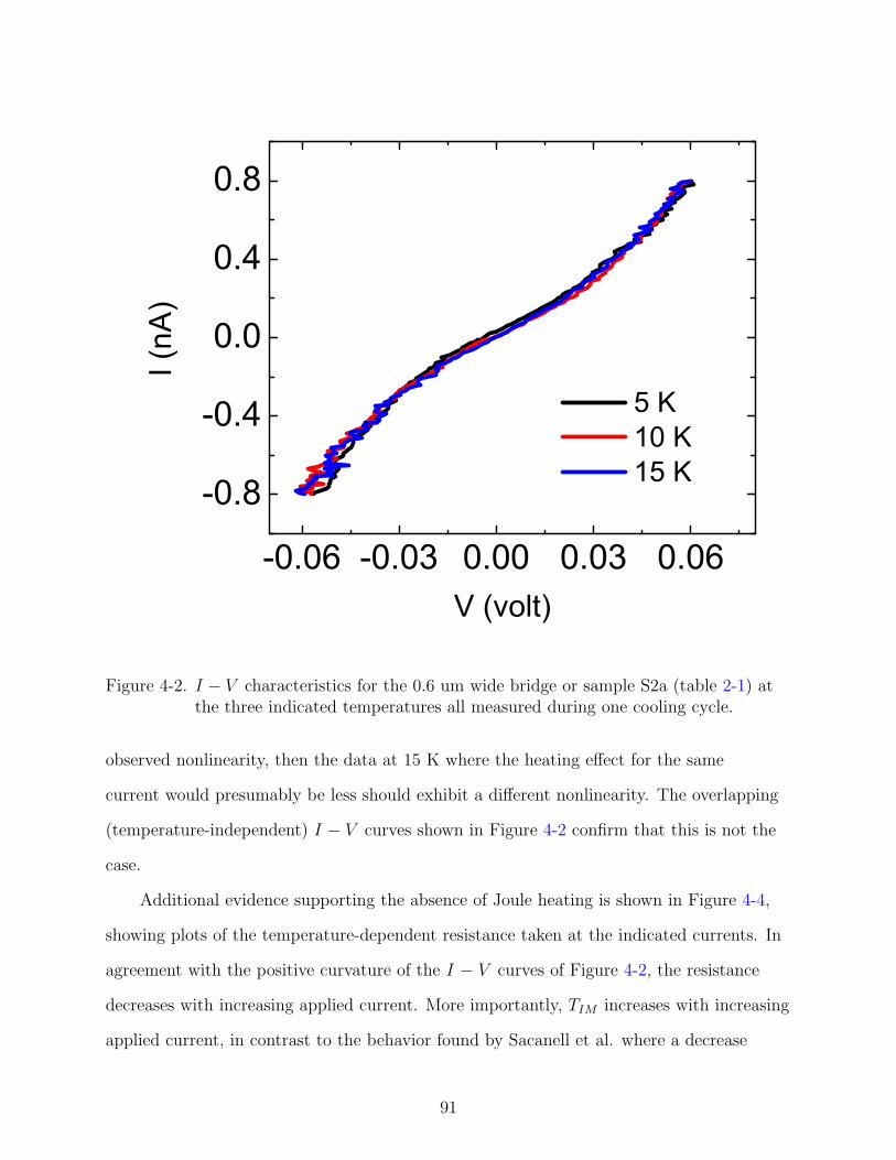
-0.06 -0.03 0.00 0.03 0.06
-0.8
-0.4
0.0
0.4
0.8
5 K 10 K 15 K
I (nA
)
V (volt)
Figure 4-2. I − V characteristics for the 0.6 um wide bridge or sample S2a (table 2-1) atthe three indicated temperatures all measured during one cooling cycle.
observed nonlinearity, then the data at 15 K where the heating effect for the same
current would presumably be less should exhibit a different nonlinearity. The overlapping
(temperature-independent) I − V curves shown in Figure 4-2 confirm that this is not the
case.
Additional evidence supporting the absence of Joule heating is shown in Figure 4-4,
showing plots of the temperature-dependent resistance taken at the indicated currents. In
agreement with the positive curvature of the I − V curves of Figure 4-2, the resistance
decreases with increasing applied current. More importantly, TIM increases with increasing
applied current, in contrast to the behavior found by Sacanell et al. where a decrease
91

-0.03 0.00 0.03
10
12
14
16
dI/d
V (n
S)
V (volt)
15 K
Figure 4-3. dI /dV -V curve at 15 K with a fit (red curve) to the Simmons’ model for arectangular barrier for sample S2a (table 2-1).
in TIM with increasing applied current is attributed to Joule heating [66]. The overall
decrease in resistance with increasing applied current may result from an electric-field
driven insulator to metal transition [67] or increased ferromagnetism resulting from spin
polarized transport [68] among other scenarios [25, 66, 69]. This effect in manganites,
which will be discussed in Chapter 5, explains the difference in the resistance values in
Figure 4-2 main panel and the inset. For instance, I − V curves were measured at fixed
temperatures in the range 45 K to 5 K using applied currents up to 1 nA, thus driving
the sample into the 1 nA current-cooled state shown in Figure 4-4. On the other hand, a
sample cooled to 15 K at zero applied current has an irreversible resistance change (see
for example, Figure 5-2) upon measuring the initial I − V curve as seen in unpatterned
thin films of LPCMO [25] and discussed in Chapter 5 for the bridges. Subsequent I − V
92

0 50 100 150108
109
1010
1011 1nA 100pA
R
()
T (K)
Figure 4-4. R(T ) curves were obtained at the indicated currents for sample S2a(table 2-1). The resistance clearly decreases with increasing applied currentwhile TIM increases with increasing applied current. This is in contrast to thebehavior found by Sacanell et al. where a decrease in TIM with increasingapplied current is attributed to Joule heating [66]
measurements reveal reproducible and reversible measurements along the lower resistance
path (not shown) [25].
4.6 Anisotropic Magnetoresistance
Next, we explore the magnetic properties of ITBs. If the formation of ITBs is linked
to the ferromagnetic domain structure of LPCMO as discussed in Section 4.2.1, the
magnetic field required for the collapse of the ITB will couple to the intrinsic magnetic
anisotropy of the thin film. Sensitivity of ITBs to magnetic field direction is verified
93

Figure 4-5. ZFC and FC resistance transitions are labeled by the field directions definedwith respect to bridge (or, sample S2a (table 2-1)) orientation in Fig 4-1.Inset: R measured at 5 K when the bridge is cooled in separate runs at theindicated fields.
in Figure 4-5 with a subset of the measured field-cooled R(T ) traces for the three field
orientations (Hx, Hy and Hz) illustrated schematically in Figure 4-1. The inset highlights
the cooling field directional dependence at 5 K. Here, after a resistance of 107 Ω is reached,
cooling in a slightly higher field results in an abrupt hundred fold drop in resistance,
suggesting a rapid and sudden disappearance of the ITB. Clearly, the in-plane fields Hx
and Hy are more effective than Hz in coupling to the magnetization to reach the low
resistance FMM state (R < 105). These observations of anisotropic field-induced ITB
extinction show a coupling of the ITBs with the magnetic easy axis which lies within the
94

plane of the film for manganites deposited on (110) NdGaO3 [1]. The magnetic field values
required to reach the low resistance state are on the order of 1 kOe, which though much
greater than the measured coercive field in unpatterned films, are not atypical for narrow
ferromagnetic wires [70]. The anisotropic MR associated with the ITBs thus suggests that
they may indeed coincide with the FMM domain boundaries forming insulating stripe
domain walls. The necessity of intrinsic phase separation for stripe domain wall formation
is apparent when considering recent measurements of notched bridges on non-phase
separated La0.67Sr0.33MnO3 which did not show the presence of highly resistive ITBs [58].
-1 0 1-40-200
2040
I (nA
)
Voltage (V)
2.0T 0.6T 0.5T 0.4T 0.3T 0.2T 0.1T 0T
Figure 4-6. I -V characteristics of the 0.6 µm wide bridge or sample S2a (table 2-1)zero-field-cooled to 15 K, measured at the indicated values of Hz
Within the context of stripe domain walls, the MR anisotropy arises when spins in
neighboring domains partially align with the field, resulting in reduced spin-dependent
scattering at the ITB (or domain wall). The large drop in resistance signifies a conversion
of the ITBs to FMM, analogous to field induced extinction of Bloch or Neel domain
95

-1 0 1-40-200
2040
I (nA
)
V/Vmax
Figure 4-7. I -V curves from Figure 4-6 for sample S2a (table 2-1) normalized to thevoltage, Vmax, measured at maximum applied current. The legend shown(lower right) in Figure 4-6 applies.
walls. This notion is confirmed in Figure 4-6 where the magnetic field dependence of
the I-V curves obtained at 15 K is shown. As Hz increases, the curvature of the I-V
curves changes (Figure 4-7). For fields sufficiently large enough to drive the bridge into a
low resistance state (≈ 9 kOe in Figure 4-5), the I-V curves become linear (Figure 4-7)
suggesting ITB extinction.
4.7 Understanding Insulating Stripe Domain Walls
4.7.1 Competing phases and strain sensitivity in (La,Pr,Ca)MnO3
As thoroughly discussed in Chapter 1, single crystals of the manganite LPCMO,
which are paramagnetic insulators with a pseudo-cubic structure at room temperature,
undergo a sudden martensitic-type structural transition within the paramagnetic
insulating (PMI) background to an antiferromagnetic charge-ordered insulating (COI)
96

phase (orthorhombic structure) below the charge-ordering temperature, TCO ≈ 200 K [29,
44, 46]. The COI phase remains nearly constant in volume fraction down to low
temperatures and an additional insulating phase, often referred to as the charge-disordered
insulating (CDI) phase is also present in bulk single crystals below TCO [29–31]. A similar
COI-CDI-FMM phase competition is expected in the thin films, although substrate strain
which modifies the manganite structure, can also modify the phase fraction. The CDI
regions (which are structurally similar to and thus possibly a remnant of the pseudo-cubic
paramagnetic phase) become, in contrast to the COI phase, predominantly ferromagnetic
upon lowering temperature. Magnetization measurements of LPCMO thin films confirm a
nearly fully FMM state for T less than the blocking temperature, TB [25]. The remaining
CDI phase which coexists with the FMM and COI phases is sometimes attributed to
accommodation strain [31] resulting from structural differences between the COI and
FMM phases.
In addition to accommodation strain resulting from intrinsic structural distortions,
the phase transitions in the LPCMO thin films deposited on NGO (110) substrates
studied here are also sensitive to strain resulting from a slight lattice mismatch with
the substrate [71]. The in-plane lattice constants of NGO (110) favor the pseudo-cubic
FMM and paramagnetic phases in LPCMO. Thus we suspect that the COI phase is either
destabilized resulting in a reduced volume fraction and increased sensitivity to applied
fields, or, completely disfavored in the 300 A-thick films on NGO as suggested by the lack
of any hysteretic features in R(T) typical of the COI phase near TCO (typically ∼ 200 K)
but rather a smooth increase down to TIM as seen in our experiment (Figure 4-1).
4.7.2 Stripe Domain Walls and the Charge Disordered Phase
Formation of high-resistance barriers in La0.7Ca0.3MnO3 have been demonstrated
by measuring low-field peaks across these barriers which span patterned constrictions
between adjacent FMM domains with extrinsically controlled spin orientations [72]. In
our bridges we suspect that it is the structural strain resulting from misaligned spins in
97

adjacent domains within the low-temperature, supercooled, predominantly FMM yet phase
separated state (Figure 4-1), coupled with the narrow dimensions of our structures, which
makes insulating stripe domain wall formation energetically favorable [53]. A significant
feature of the bridge transport properties is that the temperature dependence of resistance
below TIM varies for each cooling cycle (e.g. Figure 4-1 and Figure 4-2 show two different
zero field cooling cycles). This variation lends further support to the notion that ITBs
form due to intrinsic strain accommodation rather than local defects. Hence, we suspect
that the strain-induced CDI phase plays a vital role in the formation of ITBs.
Figure 4-8. Possible mechanisms for the formation of insulating domain walls in LPCMOthin-film bridges. (a) In the 2.5 µm wide bridge the edges have negligiblecontribution to the resistivity of the bridge due to the formation of a wide andcontinuous FMM region at low temperatures and hence the resistivity of thewire is the same as the unpatterned thin film. (b) and (c) In the 0.6 µm widebridge the edges stabilize the CDI and COI phases at the expense of the FMMphase. Insulating domain walls spanning the width of the bridge are formedeither due to the strain stabilized CDI phase as shown in (b) or a combinationof CDI and COI phases as shown in (c).
98

Two possible scenarios illustrating the role of the insulating phases in ITB formation
are shown in Figure 4-8. In both cases we show the COI phase forming at the bridge edges
since it has been shown theoretically that an anti-ferromagnetic insulating phase is favored
at the surfaces of FMM manganites [73]. Also in both cases, we depict the strain-induced
CDI phase forming at the interface between the FMM and COI phases [29]. In the first
scenario the ITBs comprising the CDI phase result from strain between two FMM regions
with misaligned magnetizations, while in the second scenario the COI phase spans the
bridge width and the ITBs comprise both COI and CDI phases. Our experiments cannot
distinguish between these two scenarios. It is possible that similar mechanisms are present
in granular LPCMO samples where, reducing the grain size also leads to metastable
states [29], as noted in Section 4.5.1.
4.7.3 Stripe Domain Walls in Relation to the Various Insulating Phases
In Chapter 3 we note that a portion of insulating phase which is not metastable in
applied fields as large as 20 kOe remains for TB < T < TIM , forming a thin barrier across
which we observe tunneling magnetoresistance (TMR). First, since the fields employed
here are not large enough to convert the COI phase to FMM [47], it is possible that this
additional insulating phase is a small amount of remnant COI present within the bridge
(panel (a) of Figure 4-9). However, a second possibility remains: a small amount of CDI
phase undergoes a metamagnetic transition to an FMM phase as the field is turned on
and then reverts back to the CDI state when the field is turned off and thus the TMR is
actually across this remaining CDI region (panel (b) of Figure 4-9). The latter scenario
provides a plausible explanation for the lack of TMR below TB (Figure 3-7) because the
CDI phase does not recover below TB when the field is turned off and thus the bridge
stays metallic. When considering the former scenario however, it is also possible that
below TB the COI phase is no longer favored due to substrate induced strain. Hence,
application of a 20 kOe field results in a metallic state with no remnant COI phase,
resulting in the lack of TMR.
99

Figure 4-9. Possible mechanisms for the formation of intrinsic tunnel junctions in thetemperature range TB < T < TIM . (a) Application of a magnetic field of 2 kOeremoves the CDI phase but the COI phase remains. When the field is removedthe remnant COI phase forms an intrinsic tunnel barrier across whichspin-polarized tunneling takes place. (b) Application of a 2 kOe field reducesthe amount of CDI phase which partially recovers when the field is removedand forms the intrinsic tunnel barrier.
4.8 Evidence of Anomalous Domain Walls in Wider, Thinner Bridges
The presence of the CDI phase, as discussed in the previous section may explain
ITB formation when reducing our bridges from 2.5 µm to 0.6 µm for the 30 nm thick
films, even though the FMM state in the 2.5 µm bridges shows nearly bulk-like transport
properties. As predicted by Golosov for ultra-thin films (2D), preliminary measurements
on 2.5 µm wide bridges fabricated from thinner, 10 nm thick films also exhibit low
temperature metastable states in the FMM phase, with the same properties as the
100

Figure 4-10. R(T ) curves obtained by cooling in three applied fields for a 2.5 µm widebridge fabricated from 10 nm thick films, or sample S3 (table 2-1). Allbridges fabricated from 10 nm thick films showed the same properties.Metastable states with high sensitivity to applied fields can be seen at lowtemperatures, reminiscent of the 0.6 µm wide bridge on a 30 nm thick film(see Figure 4-1).
0.6 µm bridges fabricated from 30 nm thick films. Figure 4-10 shows low temperature,
temperature independent high resistance states seen in the 30 nm thick, 0.6 µm wide
bridge. The dependence of ITB formation on dimensionality is currently a subject of
investigation.
4.9 Chapter Summary
In summary, we have shown that phase-separation in manganites is strongly modified
in confined geometries and leads to the formation of insulating regions thin enough to
allow direct electron tunneling, which may also coincide with domain walls separating
adjacent FMM domains [53]. Magnetotransport studies of LPCMO bridge structures
101

with submicron widths less than the average size of an FMM region enable us to observe
tunneling across these metastable intrinsic tunnel barriers with record-high resistance-area
products. The high resistance of the intrinsic tunnel barriers, is extremely sensitive to
temperature and the magnitude and direction of applied magnetic fields, giving rise to
colossal low-field magnetoresistance. In addition to offering rich physical insights into the
formation of ferromagnetic domains in phase separated systems, the presence of intrinsic
tunnel barriers introduces new opportunities for manipulating high resistance barriers on
the nanometer length scale.
102

CHAPTER 5COLOSSAL ELECTRORESISTANCE ACROSS (La,Pr,Ca)MnO3 NANOBRIDGES
5.1 Introduction
In certain manganites, just as with a magnetic field, an electric field can also produce
colossal changes in sample resistance. The effect is generally associated with some form of
phase separation in the manganite [1]. Unlike with a magnetic field however, an electric
field does not produce measurable changes in the metallic phase fraction. There is thus
speculation around several different scenarios that could potentially produce colossal
changes in resistance without changing the magnetic phase fraction. Scenarios range
from joule heating [74], a dielectric breakdown of the insulating regions [75], a change
in shape of the metallic regions [76] or a change in magnetization between neighboring
domains as a result of double exchange [1]. As in the previous chapters, here we study the
electroresistance effect on the microscopic level in the phase separated manganite LPCMO
in an attempt to capture the physics and pin point the scenario or scenarios responsible
for the observed behavior in unpatterned thin films and bulk samples.
5.2 Motivation
An understanding of the colossal electroresistance (CER) effect will surely improve
our understanding of the correlated behavior in manganites on a fundamental level. On
a more practical level, an electroresistance effect, if found at room temperature, can lead
to very practical logic applications. In this case an electric field can produce the same
‘on’ and ‘off’ functions produced by a magnetic field in the CMR and GMR devices (see
Chapter 1). As discussed in Chapters 3 and 4, when the LPCMO thin films are patterned
into narrow nanometer wide bridges, during the phase separation temperature range
alternating insulating and metallic regions can form across the length of the bridge. In
both chapters we showed very clear evidence of direct electron tunneling between two
metallic regions spanning the bridge width separated by intrinsic insulating regions. In
Chapter 4, assuming a rectangular barrier, we were able to extract a barrier height and
103
thickness with excellent fits of our data to the Simmons’ model. Tunneling measurements
in the phase separation temperature range are thus an excellent tool for probing changing
properties (i.e. changing barrier height and width of the intrinsic insulating regions)
of both the insulating and metallic regions. In the sections below we begin by briefly
reviewing the CER effect in manganites in general, followed by an introduction to the
CER effect in LPCMO thin films. Next we probe the CER effect in the LPCMO bridges
followed by a Simmons’ model analysis of the barrier properties and compare the changes
induced by an electric field with those induced by a magnetic field.
5.3 Fabrication and Measurement Techniques
For details on sample fabrication and measurement techniques for this section, please
refer to Chapter 2, Section 2.2 and also to Chapter 3. In this chapter data is presented
on two bridges: (i) Sample S2c (table 2-1), the same 0.6 µm wide, 8.0 µm long bridge
discussed in Chapters 3 and 4, and (ii) Sample S4 (table 2-1), a 0.34 µm wide, 4.0 µm long
bridge not previously discussed.
5.4 Colossal Electroresistance in Manganite Thin Films
The colossal electroresistance effect in manganites can be either extrinsic or intrinsic
in nature. Extrinsic CER effects in manganites can result from electric field gating
where itinerant carriers can be accumulated/depleted via an applied gate electric
field. In this case a gate dielectric separates a metallic gate from the manganite in
question, across which the electric field is applied. Near a phase transition boundary the
accumulation/depletion effect can result in dramatic resistivity changes. The electric field
in this case can induce an order-disorder transition extrinsically. Another type of extrinsic
effect is thought to result from the well known Schottky barrier that forms between metals
and semiconductors. In this case the schottky barrier forms between the manganite and
the metal [1, 77].
The second type of CER effect is an intrinsic electroresistance that results from
an electric field or current applied directly across the manganite sample. In this case
104

a colossal change in resistance is seen upon application of an electric field, generally
during the phase separation temperature range. The intrinsic CER effect is not yet
fully understood and a full explanation may rely on elements of the extrinsic CER
effect (namely, charge accumulation and depletion in the phase separated regions and a
non-uniform distribution of the electric field across the phase separated sample).
5.4.1 Colossal Electroresistance in (Pr,Ca)MnO3 and Related Compounds
The CER effect was first observed in Pr0.7Ca0.3MnO3 (or PCMO), one of the two
parent compounds of (La,Pr,Ca)MnO3 [78]. Within a certain temperature range, an
applied electric field induces a hysteretic first order transition to a low resistance state. It
is not completely clear weather the collapse is induced by an electric field or an electric
current though recent data [79] point to the former scenario. Like LPCMO, PCMO is also
in some contexts considered to be phase separated but requires external perturbations in
addition to temperature (such as electric or magnetic fields) to undergo an insulator to
metal transition. PCMO is phase separated into charge and orbital ordered P21nm regions
and disordered Pnma regions. In the latter case, polaron mobility is significantly increased
since charge carriers form a ‘liquid’ or interacting mobile polarons. Without electric
or magnetic field application, transport measurements reveal small polaron hopping
conduction in PCMO down to low temperatures [26, 79]. If a sufficiently high current is
applied across the sample, transport measurements reveal that charge carriers transition to
large polaron hopping. Transport measurements suggest a combination of enhanced double
exchange and an order-disorder transition associated with the CER effect [26].
Chemically doping the PCMO samples with La gives LPCMO as discussed in
Chapter 1, and induces a phase transition from a nominally charge ordered state at
room temperature to a disordered ferromagnetic metallic state at low temperatures. The
transition temperatures depend on the exact stoichiometry of the sample. Although the
root cause of the CER effect has not been studied in LPCMO, in analogy to the CER
effect in PCMO described above, one may suspect a melting of the charge ordered state
105
(i.e. order-disorder transition). In Section 5.4.2 a summary of the former scenario and
other proposed ideas on the origin of CER in phase separated manganites is presented. In
Section 5.5 our explorations of the CER effect on the nanoscale in LPCMO are presented
and the barrier parameters extracted from our data are compared to values obtained from
the literature.
5.4.2 Sources of Intrinsic Colossal Electroresistance in Manganites
Several models have been proposed in order to explain the CER effect in phase
separated manganites, namely (i) an electric field induced collapse of the charged ordered
phase (i.e. order-disorder transition) [26, 79], (ii) joule heating [74], (iii) filamentary
conduction or dielectric breakdown of the insulating regions [75], (iv) dielectrophoresis
model or spacial reorientation of the insulating and metallic phase [76], or, (v) spin
dependent domain reorientation [1].
In the case of LPCMO, an electric field induced collapse of the charge ordered phase
in favor of the disordered ferrmomagnetic metallic phase would imply an increase of the
ferromagnetic phase fraction within the film or bulk sample. This in turn would imply a
higher saturation magnetization of the thin film which is contrary to observation [25, 75].
In the second joule heating scenario, the temperature of sample increases due to large
current densities, changing the effective phase fractions. In this case, the apparent
temperature of the sample as read by a thermostat in the vicinity of the sample is
different than the actual temperature. For our samples, we have ruled out joule heating as
described in detail in Section 4.5.2. Below, in Section (5.5), our tunneling measurements
reveal that the third scenario above (filamentary conduction) can be ruled out while
the dielectrophoresis model may indeed help explain the CER effect observed in our
nanobridges and thus perhaps also in phase separated manganites. As also discussed
below, we cannot however rule out the fifth and final scenario of spin dependent domain
reorientations which may result from an enhanced double exchange mechanism induced by
higher current densities.
106

5.5 Colossal Electroresistance in Patterned and Unpatterned(La,Pr,Ca)MnO3 Thin Films
The CER effect was studied on LPCMO thin films by Amlan Biswas and students [25].
Subsequently, thin films prepared identical to this CER study were patterned into
nanometer wide bridges presented below. It was found that within the phase separation
temperature range the application of an electric field resulted in an irreversible change to a
lower resistance state. Despite the change in resistance, magnetization measurements did
not reveal an increase in the ferromagnetic metallic phase fraction within the films. The
transition to a lower resistance state is smooth in thin films, though with a well defined
critical voltage (or current) as shown in Figure 5-1. Current-voltage (I − V ) characteristics
for this 10 µm wide LPCMO film reveal a clear transition to a lower resistance state
upon increasing current. The relative concentrations of the La and Pr were varied to
change the range of phase separation temperatures and it was found that regardless of the
temperature window, the effect remained the same in all films within the phase separation
range.
A reversible, colossal CER effect has been reported in LPCMO films with Fe
substitutions at the Mn site [80]. The mechanisms for the CER effect in the Fe doped
films compared to undoped LPCMO may not be wholly different. In undoped LPCMO,
the charge ordered phase and the ferromagnetic metallic phase are very close in free
energy though with lowering temperature, the metallic phase has an increasingly lower free
energy. This energy landscape is certainly altered in the case of Fe doped LPCMO. In this
case the metallic phase may not be preferred over the insulating phase, just as in PCMO
thin films [26].
In the bridges fabricated from LPCMO thin films, the CER effect is evident when
measuring R(T ) at different applied currents as shown in Figure 5-1. The several order of
magnitude change in the low temperature resistance with applied electric field can well be
described in the intrinsic tunneling framework discussed in Chapter 4.
107
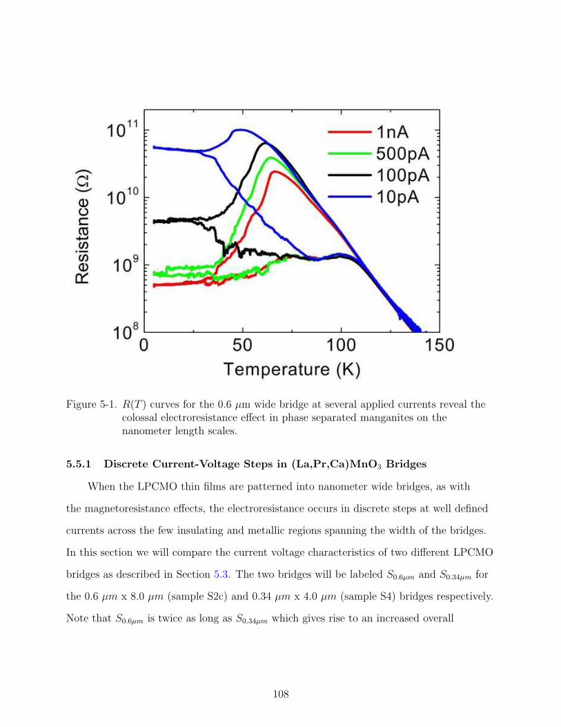
Figure 5-1. R(T ) curves for the 0.6 µm wide bridge at several applied currents reveal thecolossal electroresistance effect in phase separated manganites on thenanometer length scales.
5.5.1 Discrete Current-Voltage Steps in (La,Pr,Ca)MnO3 Bridges
When the LPCMO thin films are patterned into nanometer wide bridges, as with
the magnetoresistance effects, the electroresistance occurs in discrete steps at well defined
currents across the few insulating and metallic regions spanning the width of the bridges.
In this section we will compare the current voltage characteristics of two different LPCMO
bridges as described in Section 5.3. The two bridges will be labeled S0.6µm and S0.34µm for
the 0.6 µm x 8.0 µm (sample S2c) and 0.34 µm x 4.0 µm (sample S4) bridges respectively.
Note that S0.6µm is twice as long as S0.34µm which gives rise to an increased overall
108
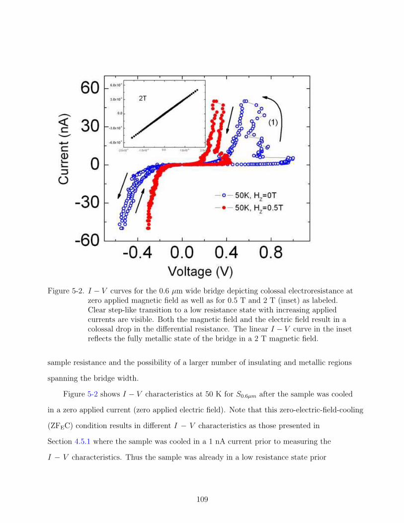
Figure 5-2. I − V curves for the 0.6 µm wide bridge depicting colossal electroresistance atzero applied magnetic field as well as for 0.5 T and 2 T (inset) as labeled.Clear step-like transition to a low resistance state with increasing appliedcurrents are visible. Both the magnetic field and the electric field result in acolossal drop in the differential resistance. The linear I − V curve in the insetreflects the fully metallic state of the bridge in a 2 T magnetic field.
sample resistance and the possibility of a larger number of insulating and metallic regions
spanning the bridge width.
Figure 5-2 shows I − V characteristics at 50 K for S0.6µm after the sample was cooled
in a zero applied current (zero applied electric field). Note that this zero-electric-field-cooling
(ZFEC) condition results in different I − V characteristics as those presented in
Section 4.5.1 where the sample was cooled in a 1 nA current prior to measuring the
I − V characteristics. Thus the sample was already in a low resistance state prior
109
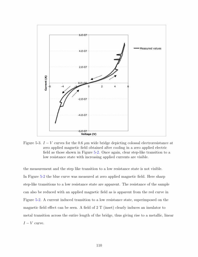
Figure 5-3. I − V curves for the 0.6 µm wide bridge depicting colossal electroresistance atzero applied magnetic field obtained after cooling in a zero applied electricfield as those shown in Figure 5-2. Once again, clear step-like transition to alow resistance state with increasing applied currents are visible.
the measurement and the step like transition to a low resistance state is not visible.
In Figure 5-2 the blue curve was measured at zero applied magnetic field. Here sharp
step-like transitions to a low resistance state are apparent. The resistance of the sample
can also be reduced with an applied magnetic field as is apparent from the red curve in
Figure 5-2. A current induced transition to a low resistance state, superimposed on the
magnetic field effect can be seen. A field of 2 T (inset) clearly induces an insulator to
metal transition across the entire length of the bridge, thus giving rise to a metallic, linear
I − V curve.
110

Figure 5-3 shows I − V curves for S0.34µm after (ZFEC) to 85K. It is evident from
comparing the quality of data for S0.34µm vs. S0.6µm that the data for the former is more
appropriate for purposes of analysis given the far greater signal to noise ratio. This fact
is probably related to the fact that S0.6µm is twice as long in length as S0.34µm and thus
contains perhaps only one, but certainly fewer insulating regions along the length of
the bridge. S0.6µm however shows a much more dramatic CER effect. In this figure, the
vertically lower arrow for increasing current (increasing voltage) shows the first leg of the
curve and a transition to a lower state is very clear. Beyond the first transition, small
spikes to an even lower resistance state (see top left quadrant, Figure 5-4B) are visible
though the sample does not make a complete transition to that lower state.
A B
Figure 5-4. Each branch of the the ZFEC I − V curve for the 0.34 µm wide bridge shownin Figure 5-3 was first differentiated and the derivative was fit to the quadraticSimmons’ model. A. shows the dI/dV vs. V plot for the center (red)numerically generated fit shown in B. B. shows numerical fits using theSimmons’ model to each branch of the I − V curve obtained at 85K for zeroapplied magnetic field and cooled in zero applied electric field.
To analyze the data shown in Figure 5-3, each segment of the I − V curve was
differentiated numerically with respect to voltage and fit to the Simmons’ model (see
Section 4.5.1 for details) with the barrier height and width set as free parameters.
Excellent fits to the Simmons’ model (dI/dV ∼ V 2) were obtained for voltages below
111

3.5 V. Figure 5-4A shows a dI/dV curve and quadratic fit to the Simmons’ model for the
central branch of the I − V curve shown in Figure 5-3. Figure 5-4B shows the simulated
I − V curves for each branch of the original (ZFEC). Note that the simulated I − V curve
resulting from the bottom branch of the bottom left (third) quadrant depicts a state that
well describes the brief drops in resistance (or spikes) in the first quadrant since they fall
approximately on the yellow curve. The barrier heights and widths derived from each fit
are labeled in the legend of Figure 5-4B and are discussed in detail in the next section.
5.5.2 Analyzing Changes in Barrier Properties Using Simmons’ Model
Figure 5-5. Barrier heights and widths obtained using the Simmons’ model for the0.34 µm wide bridge as a function of the critical electric current during theinitial increase of applied current (i.e., first quadrant—top right—bottomI − V curve branch.
Figure 5-5 shows a plot of barrier height and width as a functions of the critical
current required to go to each state along the first quarter of the I − V curve (bottom
curve, first quadrant) shown in Figures 5-3 and 5-4. First we note that the barrier
heights, which are on the order ∼0.1 eV are on the order of the polaronic hopping
activation energy reported in the parent compound PCMO [26, 79] and also from our
own complex analysis of the LPCMO dielectric properties (unpublished work). Contrary
to expectations, the barrier height appears to increase by approximately 44% while the
barrier width decreases by nearly 18%. Intuitively and given the decreasing resistance,
112

a canting of the spins within the charge-ordered barrier may be expected. However, an
increasing barrier height translates to a more ‘robust’ barrier, or less spin canting and
better antiferromagnetic coupling, given the double exchange nature of manganites in
general. The decreasing barrier width on the other hand translates to the insulating region
becoming narrower in width which is not necessarily contrary to intuition.
With the fit to the simple rectangular tunnel barrier using Simmons’ model as a
first order approximation, the dielectrophoresis model may be invoked for a consistent
explanation. In this case, prior to application of an electric field or current the naturally
formed intrinsic insulating regions can be approximated as ‘imperfect’, containing small
defects centers in the form of ferromagnetic islands or small magnetic polarons. Upon
application of an electric field the small ferromagnetic regions or polaronic droplets within
the insulating regions move toward the metallic regions and coalesce. In this way, the
volume of neither phase fraction increases but rather it reorders spatially. In this way, the
insulating regions contain less co-tunneling or pinning centers and increase in quality and
thus barrier height while the metallic regions are now separated by a thinner barrier and
are thus more closely spaced. Thus qualitatively, the dielectrophoresis model may indeed
capture the dynamics of the CER effect.
5.5.3 Comparing Changes in Barrier Properties for Applied Electric vs.Magnetic Fields
In order to understand the fundamental differences between the CMR and CER
effects within the phase separation temperature range, we study the changes in barrier
properties with the application of a magnetic field. The I − V curves shown in Figure 4-6
for sample S0.6µm were also fit to the Simmons’ model as shown in Figure 5-6. Given
the relative noise level for this sample, the barrier heights extracted from the fits to the
Simmons’ model were on the order of the energy gap of PCMO, though rather high. This
may be due to the presence of several tunnel barriers in series, given the relatively longer
length of the bridge.
113

Figure 5-6. Barrier heights and widths obtained using the Simmons’ model for the 0.6 µmwide bridge as a function of the applied magnetic field.
Again, with the Simmons’ model as a first order fit to our I − V curves, a clearly
different trend in the barrier widths and heights with increasing magnetic fields is evident
than for the CER effect. Here, with increasing applied field, there is a clear reduction
of the barrier heights (86%) while the barrier width remains relatively constant with a
small increase of approximately 16%. This decrease in barrier height can be understood
in terms of spin canting of the antiferromagnetically ordered insulating barrier spins in
the direction of the applied magnetic field. The spin canting increases with increasing
magnetic field and the barrier width reduces for the tunneling electrons which are also
oriented in the direction of the field. The barrier width however remains nearly the same
indicating a sudden collapse of the insulating barrier at a well defined critical field rather
than a gradual decrease in width with increasing ferromagnetic phase fraction.
5.5.4 Shortcomings of the Rectangular Barrier Simmons’ Model
The rectangular barrier Simmons’ model generally describes insulator-metal tunnel
junctions with abrupt interfaces quite well but is well know to have shortcomings when
characterizing tunnel junctions with non-negligible amounts of interface roughness,
spin polarized electrodes, spin canting at the edges of the tunnel barrier or other
insulator-metal interface states [1]. To depict such barrier properties more realistically,
we are currently employing a method which models the tunnel barrier as a double barrier
114

within the Simmons’ rectangular barrier model with fits derived from four parameters:
two barrier heights and two barrier thicknesses [81]. The authors of this technique
were able to deduce a mild correlation in their barrier heights and widths by utilizing
this technique. A second technique requires obtaining rms roughness values of the
interface and incorporating the roughness as changing barrier widths of rectangular
barriers (approximated as a gaussian distribution) within the Simmons’ model [82]. Both
models are presently being tested for their effectiveness. The current analysis is a work in
progress.
5.6 Chapter Summary
In summary, we have shown that tunneling measurements across the intrinsic phase
separated regions along the length of nanometer wide LPCMO bridges can be utilized
as a tool to characterize the colossal electroresistance (CER) effect in phase separated
manganites on the nanometer length scales. In analogy to the colossal magnetoresistance
(CMR) effect, an applied electric field can give rise to a colossal decrease in resistance.
Tunneling measurements allow us to clearly decipher the unique effects of each type of
external perturbation (i.e. electric or magnetic field) on the intrinsic tunnel junctions
(intrinsic insulating and metallic regions). Fits to the Simmons’ model reveal a decrease
in the barrier height with increasing magnetic field while the barrier width remains
relatively constant. An increasing electric field however results in a decreasing barrier
width but an increasing barrier height. Thus the CER and CMR effects are fundamentally
different. The CER effect may best be explained by a spatial reorganization of the
intrinsic insulating and metallic regions while the CMR effect may be described by a field
induced collapse of the charge ordered insulating state.
115
CHAPTER 6COLOSSAL MAGNETOCAPACITANCE AND ANISOTROPIC TRANSPORT IN
(La,Pr,Ca)MnO3 THIN FILMS
6.1 Introduction
In this chapter1 we report on the use of an unconventional trilayer configuration
in which the sample under investigation, in our case a 600 A thick LPCMO film,
comprises the base layer of a metal-insulator-metal (MIM) trilayer capacitor structure
(see Figures 6-1 and 2-12). Under certain experimental conditions this unconventional
configuration allows for the simultaneous measurement of electrical transport both
parallel and perpendicular to the film interfaces. Although the four-terminal Van der
Pauw measurement of the LPMCO films provides unambiguous information about
transport parallel to the film interfaces, the two-terminal capacitance measurement is more
problematic since it includes contributions from both parallel and perpendicular transport.
By using complex circuit analysis, we show that the two-terminal perpendicular
contribution to electronic transport can dominate over the parallel contribution provided
certain experimental constraints are satisfied. When these conditions are satisfied, we
show using the well-known Maxwell-Wagner model that the perpendicular contribution is
resolved into two series-connected parts: a contribution from the reference AlOx capacitor
and a contribution from the intrinsic dielectric response of the LPCMO film. We then
show with additional data on films of different thickness how the substrate strain-induced
anisotropy, measured by the difference in temperature between the resistance maxima
and capacitance minima decreases and approaches bulk like behavior as the film thickness
increases.
1 Portions of the content in this chapter have been published in the journal NaturePhysics in a Letter entitled “Colossal magnetocapacitance and scale-invariant dielectricresponse in phase-separated manganites” [59]
116

We distinguish two distinct strain-related direction-dependent insulator-metal (IM)
transitions and use Cole-Cole plots to establish a heretofore unobserved collapse of the
dielectric response onto a universal scale-invariant power-law dependence over a large
range of frequency, temperature and magnetic field. The resulting phase diagram defines
an extended region where the competing interaction of the coexisting ferromagnetic metal
(FMM) and charge-ordered insulator (COI) phases [83–88] have the same behavior over
a wide range of temporal and spatial scales. At low frequency, corresponding to long
length scales, the volume of the phase diagram collapses to a point defining the zero-field
IM percolation transition in the perpendicular direction. This method thus also allows
for a novel probe of phase boundaries in thin films, where the boundaries may not be
straightforward to detect with dc transport measurements.
6.2 Motivation
A full characterization of phase separation and the competition between phases is
necessary for a comprehensive understanding of strongly-correlated electron materials
(SCEMs), as discussed in Chapter 1. The dc transport measurements presented in the
preceding chapters (which are analogous to those performed on the narrow bridges
presented in this work) are not sensitive to exact phase fractions and the dielectric
properties of the insulating phases. In addition, the dc transport measurements cannot
distinguish between two different insulating phases which would result in the same
hopping transport temperature dependence. Ac measurement techniques on the other
hand can distinguish between different dielectric constants and phase fractions using
complex analysis. In this chapter we probe phase separation in LPCMO thin films
by analyzing the dielectric response of the thin films embedded in an unconventional
geometry as described in Section 2.3. Thin films of SCEMs such as LPCMO are often
grown epitaxially on planar substrates and typically have anisotropic properties that are
usually not captured by edge-mounted four-terminal electrical measurements, which are
primarily sensitive to in-plane conduction paths. Accordingly, the correlated interactions
117

in the out-of-plane (perpendicular) direction cannot be measured but only inferred. We
address this shortcoming and show here an experimental technique in which the LPCMO
film serves as the base electrode in a metal-insulator-metal (MIM) trilayer capacitor
structure. This unconventional arrangement allows for simultaneous determination of
colossal magnetoresistance (CMR) associated with dc transport parallel to the film
substrate and colossal magnetocapacitance (CMC) associated with ac transport in the
perpendicular direction.
6.3 Methods
Trilayer LPCMO–AlOx–Al capacitors were formed as described in detail in Chapter 2.
For the particular capacitor structure studied in this chapter, the LPCMO thin film was
600 A thick while the AlOx dielectric was 100 A thick.
As described in Section 2.5.3, the capacitance measurements (Figure 6-1, red)
were made using an Andeen-Hagerling AH 2700A Capacitance Bridge in a guarded
three-terminal mode at stepped frequencies ranging from 50-20,000 Hz. Two of the
terminals were connected to the sample leads shown schematically in Figure 6-1 and the
third to an electrically isolated copper can surrounding the sample and connected to the
ground of the bridge circuit. Most of the measurements were made using 25 mV rms
excitation, and linearity was confirmed at all fields and temperatures. The bridge was
set to output data in the parallel mode in which the sample is assumed to be the circuit
equivalent of a capacitance C in parallel with a resistance R (see Section 6.4).
Contacts to the sample were made to the base LPCMO film using pressed indium and
to the Al counterelectrode using fine gold wire held in place with silver paint. Silver paint
was also occasionally used to make contact to the base electrode with no consequence
to the capacitance data at all measurement frequencies. The series combination of the
LPCMO parallel resistance with the leakage resistance of the AlOx dielectric was found to
be immeasurably large with a lower bound > 1010 Ω determined by replacing the sample
118
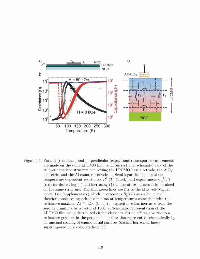
Figure 6-1. Parallel (resistance) and perpendicular (capacitance) transport measurementsare made on the same LPCMO film. a, Cross sectional schematic view of thetrilayer capacitor structure comprising the LPCMO base electrode, the AlOx
dielectric, and the Al counterelectrode. b, Semi logarithmic plots of thetemperature dependent resistances R↓↑
|| (T ) (black) and capacitances C↓↑⊥ (T )
(red) for decreasing (↓) and increasing (↑) temperatures at zero field obtainedon the same structure. The thin green lines are fits to the Maxwell-Wagnermodel (see Supplementary) which incorporates R↓↑
|| (T ) as an input andtherefore produces capacitance minima at temperatures coincident with theresistance maxima. At 50 kOe (blue) the capacitance has increased from thezero field minima by a factor of 1000. c, Schematic representation of theLPCMO film using distributed circuit elements. Strain effects give rise to aresistance gradient in the perpendicular direction represented schematically byan unequal spacing of equipotential surfaces (dashed horizontal lines)superimposed on a color gradient [59].
119

with a standard 1010 Ω ceramic resistor. Thus the leakage resistance is more than a factor
of 1000 higher than the ∼10 MΩ maximum resistance of our LPCMO film (Figure 6-1).
The four-terminal resistance measurements of dc transport parallel to the film
interfaces (Figure 6-1, black) were made using evenly spaced Van der Pauw contacts (not
shown in Figure 6-1) directly connected at the LPCMO film edges. To check for any
frequency dependence in the parallel resistance of the LPCMO and associated contact
resistance, we performed a two-terminal ac measurement by applying a sinusoidal voltage
to all pairs of the LPCMO contacts and used a lock-in amplifier to synchronously detect
the output of a wide band current amplifier that provided a return path to ground for
the sample current. The two-terminal resistance was quite similar to the four-terminal
measurement. Importantly, no frequency dependence in the range 50-20,000 Hz for the
resistance varying from 1 KΩ to 20 MΩ (Figure 6-1) was detected, thus assuring that all
the frequency dependence seen in the capacitance measurement is due to perpendicular
rather than parallel transport. In addition, we established in separate experiments on
symmetric Al–AlOx–Al structures that CAlOx has negligible frequency dispersion over the
same frequency range.
6.4 Comparison of Longitudinal and Perpendicular Voltage Drops
The measured voltage of the two-terminal configuration of Figure 6-1 can have
both parallel and perpendicular contributions from currents flowing respectively either
along the LPCMO electrode or transverse to the film through the capacitor. Since these
contributions cannot be distinguished in a two-terminal measurement, it is necessary
when measuring capacitance to establish conditions where the perpendicular voltage drop
dominates over the parallel voltage drop. There are two necessary requirements to assure
a dominant perpendicular voltage drop: (1) the dc leakage current through the AlOx
dielectric is negligible and (2) the measurement frequency is constrained to be within well
defined upper and lower bounds determined by sample properties.
120

We can begin to understand these requirements by modeling the measurement
configuration as a resistance RS in series with the parallel combination of a complex lossy
capacitance, C∗(ω) = C1(ω) − iC2(ω), and a dc resistance, R0 (Figure 6-1). By lossy
capacitance we mean a capacitor that does not pass dc current but does experience loss at
ac due to dipole reorientation. Thus the combination of C∗(ω) shunted by R0 is a leaky
capacitor which does pass dc. The resistance RS includes the parallel resistance R|| of the
LPCMO and any resistance associated with the LPCMO contact. The negligible resistance
of the Al counterelectrode and its associated contact are included in RS.
Our measurements at dc establish the conditions R0 + RS > 1010 Ω (Section 6.3)
and maxRS = 107 Ω (Figure 6-1), which together imply that over the whole range of dc
measurements more than 99.9% of the voltage appears across C∗. At temperatures away
from the resistance peak this figure of merit improves considerably.
Since the capacitance measurements are made at finite frequency, we must consider
the more complicated situation of additional current paths and choose conditions to assure
that most of the ac potential drop is across C∗(ω). We do this by redrawing the circuit
of Figure 6-2 to include the ac loss as a resistor R2(ω) = 1/ωC2(ω) (Figure 6-2) which
diverges to infinity at dc (ω = 0). To be sensitive to LPCMO properties, we desire most of
the ac current to flow through R2(ω) and therefore choose frequencies to satisfy
R2(ω) =1
ωC2(ω)¿ R0 = 1010 Ω (6–1)
thereby determining a lower bound on ω.
The AH capacitance bridge reports the capacitance C ′(ω) and the conductance
1/R(ω) of the parallel equivalent circuit shown in Figure 6-2. Using straightforward circuit
analysis we relate the measured quantities C ′(ω) and R(ω) to the circuit parameters of
Figure 6-2 by the equations:
C ′(ω) = C1(ω)((R2(ω))2
(R2(ω) + RS)2 + (R2(ω)ωRSC1)2), (6–2)
121

Figure 6-2. Circuit diagrams facilitate understanding the sources of longitudinal andperpendicular voltage drops. a, Circuit equivalent of the two-terminalmeasurement configuration (Figure 6-1) where RS is the series resistance of theLPCMO sample and the parallel combination of a complex (lossy) capacitorC∗(ω) with a resistor R0 represents the impedance of the LPCMO in serieswith the aluminum oxide capacitor. In the two-terminal configuration, thelongitudinal voltage drop across Rs cannot be distinguished from theperpendicular voltage drop across the parallel combination of C∗(ω) and R0.b, Decomposition of C∗(ω) = C1(ω)− iC2(ω) into a parallel combination ofC1(ω) and R2(ω) = 1/ωC2(ω). c, Circuit equivalent for the capacitance C ′(ω)and conductance 1/R(ω) reported by the capacitance bridge. d,Maxwell-Wagner circuit equivalent for the LPCMO impedance in series withthe Al/AlOx capacitor. The LPCMO manganite film impedance is representedas a lossy capacitor C∗
M(ω) shunted by a resistor RM . There is no shuntingresistor across CAlOx because the measured lower bound on R0 is 10 GΩ, wellabove the highest impedance of the other circuit elements.
122

and
R(ω) =(R2(ω) + RS)2 + (ωR2(ω)RSC1(ω))2
(R2(ω) + RS) + (ωR2(ω)RSC1)2. (6–3)
If RS is small enough to satisfy the relation
RS ¿ min
1
ωC1(ω),
1
ωC2(ω),
1
ωC1(ω)(ωC2(ω)
ωC1(ω))
, (6–4)
then equations 6–1 and 6–2 reduce respectively to C ′(ω) = C1(ω) and R(ω) = R2(ω).
Accordingly, the fulfillment of the constraints imposed by equations 6–1 and 6–4 assures us
that the ac dissipation is not due to leakage resistance and that the voltage drop across RS
can be ignored. Under these conditions the measured complex capacitance has real, C ′(ω),
and imaginary, C ′′(ω) = 1/ωR(ω), parts that reflect respectively the polarization and the
dissipation plotted and discussed in Section 6.7.
The constraints of equations 6–1 and 6–4 now become
1
ωC ′′(ω)¿ R0 = 1010Ω (6–5)
RS ¿ min
1
ωC ′(ω),
1
ωC ′′(ω),
1
ωC ′(ω)(ωC ′′(ω)
ωC ′(ω))
, (6–6)
where we have replaced C1 and C2 by the measured quantities C ′ and C ′′ respectively.
These relations conveniently allow us to experimentally determine the range of frequencies
over which RS can be safely ignored, thus guaranteeing that the equipotentials at ac are
parallel to the film interface (Figure 6-1). We show in Figure 6-3 the H = 0 temperature
dependence of the impedance components, 1/ωC ′(ω), 1/ωC ′′(ω) measured at 500 Hz
and R|| measured at dc. The corresponding temperature dependence of C ′(ω) is shown
in Figure 6-1. Clearly the constraints of equations 6–5 and 6–6 are satisfied. It is not
necessary to plot the third component of 6–6 since C ′′(ω) > C ′(ω) for all of our data in the
region of collapse (see Figure 6-3). We have verified that the constraints hold up to 20 kHz
at all the temperatures and fields used to construct the phase diagram in Figure 6-8.
For our lowest frequency of measurement (100 Hz) we calculate C ′′ = 0.16 pF as a lower
123
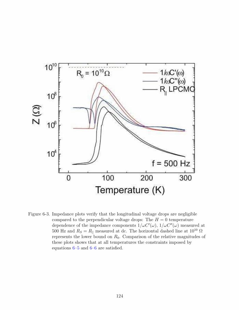
Figure 6-3. Impedance plots verify that the longitudinal voltage drops are negligiblecompared to the perpendicular voltage drops: The H = 0 temperaturedependence of the impedance components 1/ωC ′(ω), 1/ωC ′′(ω) measured at500 Hz and RS = R|| measured at dc. The horizontal dashed line at 1010 Ωrepresents the lower bound on R0. Comparison of the relative magnitudes ofthese plots shows that at all temperatures the constraints imposed byequations 6–5 and 6–6 are satisfied.
124

bound below which equation 6–5 cannot be satisfied. For all of our data, C ′′(100 Hz)
is more than a factor of ten higher and equation 6–5 is thus satisfied for all of our low
frequency data.
6.5 Maxwell-Wagner Analysis
Having established the experimental conditions that allow us to ignore the series
voltage drop across RS, we now must distinguish the dielectric responses of the manganite
film and the AlOx capacitance. We model C∗(ω) using a Maxwell-Wagner (MW) circuit
equivalent (Ref. 16) in which impedance is represented as the series connection of two
leaky capacitors. This configuration is often used to account for the effect of contacts in
dielectric measurements. In our case the manganite impedance, expressed as a parallel
combination of a resistance RM and capacitance CM , is connected in series with a leak
free capacitance CAlOx representing the Al/AlOx circuit element shown in Figure 6-2. The
resulting expression,
C∗(ω) = C∗MW (ω) =
CAlOx
1 + iwRMCAlOx
1+iwRMCM
, (6–7)
reveals a dielectric response determined by two time constants, RMCAlOx and RMCM . As
ω increases, the capacitance crosses over from being dominated by CAlOx to a capacitance
dominated by the series combination of CAlOx and CM . If CM ¿ CAlOx, as it is over much
of the data range in Figure 6-1 and likewise for similar data taken in high magnetic fields,
then C∗ in the high frequency limit is equal to CM and is therefore a direct measure of the
LPCMO dielectric response. We test these limits in Figure 6-1 by evaluating ReC∗MW (ω)
at 0.5 kHz (green curve) using CM/CAlOx = 10−4 and RM = R||(T )↓↑ (black) as inputs.
CM is assumed to be real for this calculation. The MW model thus provides a good
qualitative account of the temperature-dependent capacitance (Figure 6-1, green line)
for CM independent of frequency and equal to 10−4 CAlOx. The MW model also shows
good alignment in temperature between the maximum in the resistance used as an input
and the calculated capacitance minimum. Finally, we note that the large series-connected
aluminum oxide capacitor serves as a reference capacitor, which by its presence decloaks
125
or makes visible the smaller manganite capacitance. If the frequency becomes too high,
the constraint in equation 6–6 is violated and RS becomes visible, introducing longitudinal
voltage drops that cannot be distinguished from the perpendicular drops.
In reality there is considerable dielectric loss, especially in the presence of magnetic
field, and CM is frequency dependent and therefore complex. If we force CM in the MW
calculation to be complex with, for example, a Debye response, the alignment between the
resistance maximum and the capacitance minimum does not change. The Cole-Cole plots
(Figures 6-6 and 6-7) are the additional ingredients that clearly capture the interesting
intrinsic dynamics of scale invariant dielectric response associated with the interplay of
competing phases as discussed in Section 6.7.
It is worthwhile to further elaborate on intrinsic versus extrinsic effects. The MW
model is usually used to ascertain the contributions of contacts and interfaces when the
material of interest is sandwiched between two electrodes [6, 89–92]. In capacitors with
thick dielectrics, the interface region next to either electrode can have distinctly different
properties than the interior bulk. Such a heterogeneous system is well described in the
MW model by two series-connected leaky capacitors. If one of the leakage components,
say the interface, is magnetic field sensitive and exhibits magnetoresistance (MR), then the
measured magnetocapacitance (MC) can be a consequence of the extrinsic properties of
an interface contact rather than the intrinsic properties of the bulk. In the unconventional
configuration described here, the interface contact is a dispersionless leak-free Al–AlOx
capacitor as represented schematically in Figure 6-1, and the observed MC is due to the
intrinsic properties of the mixed phase LPCMO. Any interface effects between the AlOx
and the LPCMO are negligible, since the factor of 1000 change in capacitance, which
includes the region where power-law scaling collapse is observed, necessarily involves the
entire manganite film. In addition all extrinsic contributions from contacts to the LPCMO
at the film edges (Figure 6-1) are included in the resistance RS, which as we have shown
above, can be ignored when the frequency is chosen to satisfy the inequality of equation
126

6–6. Experimentally, this insensitivity was further checked by using silver paint or pressed
indium for contacts as described in Section 6.3.
6.6 Dependence of Anisotropy on Film Thickness
The insulator to metal (IM) transition in bulk LPCMO is due to a 3D percolation
transition. However, as described in the preceding sections, the presence of strain at
substrate/LPCMO interface gives rise to anisotropy as measured by two distinct IM
transitions: one in the parallel direction, T ↓↑IM,||, corresponding to resistance maxima, and
the other in the perpendicular direction, T ↓↑IM,⊥, corresponding to capacitance minima.
To verify that the strain-induced anisotropy decreases for thicker more bulk-like films,
we have repeated the measurements at zero field for a set of films with three different
thicknesses: d = 300 A , 600 A and 900 A .
Figure 6-4 shows the dependence of T ↓↑IM,|| and T ↓↑
IM,⊥ on d for cooling and warming
as labeled in the legend. For parallel transport the observed increase of transition
temperatures can be qualitatively explained by the effect of dimensionality on percolation.
Since percolation in 3D occurs at a lower metal fraction than it does in 2D, the IM
transition increases with increasing d as is indeed observed. This qualitative picture
is complicated however by the presence of a strained layer at the substrate interface
which contains a higher fraction of FMM phase. In this case conduction in the parallel
direction is facilitated by the presence of the higher conductivity strained layer whereas
in the perpendicular direction the current paths must thread regions containing a greater
proportion of insulating phase, hence the difference between T ↓↑IM,|| and T ↓↑
IM,⊥. The
temperature differences, ∆T ↓↑IM = T ↓↑
IM,|| − T ↓↑IM,⊥, for cooling and warming are plotted
versus d in Figure 6-5. We note that the anisotropy does indeed decrease with increasing
d. Thus as d increases the IM transition moves to higher temperature and transport
becomes more isotropic as the effect of the strained interface diminishes.
The films discussed above were prepared from the same target but under different
conditions than the 600 A -thick film discussed in this chapter. The deposition conditions
127

Figure 6-4. With increasing LPCMO thickness d the anisotropic IM transitions move tohigher temperatures: The transition temperatures associated with resistancemaxima (squares and circles) and capacitance minima (triangles) are identifiedin the legend and plotted as a function of d for cooling and warming. Thecapacitance data for the three different films are taken at 100 Hz and satisfythe impedance inequalities expressed in equations 6–5 and 6–6 and shown inFigure 6-3 for the 600 A -thick sample.
(oxygen pressure = 420 mTorr, substrate temperature = 820oC, deposition rate =
0.5 A /s) were determined by minimizing the transition width at an IM transition
temperature ( T ↓IM,||) that is close to the maximum value(cooling) observed in bulk
compounds of the same composition. The target was then conditioned with the same
deposition parameters for many runs. In comparing the two 600 A -thick films, we see that
the transition temperatures T ↓IM,|| = 117.7 K and T ↑
IM,|| = 140.5 K of the optimized
600 A -thick film shown in Fig. 6-4 are appreciably higher than the corresponding
temperatures, T ↓IM,|| = 95 K and T ↑
IM,|| = 106 K, of the film shown in Figure 6-1. In
128

Figure 6-5. With increasing LPCMO thickness the anisotropy as measured by∆T ↓↑
IM = T ↓↑IM,|| − T ↓↑
IM,⊥ decreases towards zero and bulk like behavior: Thedata for both cooling and warming cycles at each thickness are obtained fromthe data shown in Figure 6-5 by subtracting the temperature of thecapacitance minimum (perpendicular transition) from the temperature of theresistance maximum. The error bars, which are on the order of the symbol sizein Figure 6-5, are determined by the temperatures which give a ± 0.1%deviation at each extremum (resistance maximum or capacitance minim um).
addition, the respective anisotropies for cooling (∆T ↓IM = 1.5 K) and warming (∆T ↑
IM =
3.5 K) of the optimized 600 A -thick film are significantly smaller than the corresponding
anisotropies for cooling (∆T ↓IM = 20 K) and warming (∆T ↑
IM =15 K) of the same thickness
film shown in Figure 6-1. These results show that our technique can advantageously be
used to correlate anisotropies in LPCMO with deposition parameters. We anticipate that
this capability will be applicable to other strongly-correlated complex oxide systems as
well.
129

6.7 Scale Invariant Dielectric Response
The simultaneous measurement of the zero field (H = 0) parallel resistance R||(T )
and perpendicular capacitance C(T ) transport in the LPCMO film, which is the base
electrode in the trilayer configuration shown schematically in Figure 6-1, is captured in the
temperature-dependent curves shown. The two-terminal C(T ) measurements correspond
to the real part C ′(ω) of a complex lossy capacitance, C∗(ω) = C ′(ω) − iC ′′(ω), measured
at f = ω/2π = 0.5 kHz. As temperature T decreases from 300 K, the prevailing high
temperature paramagnetic insulator (PI) phase gives way near T = 220 K [87] to a
dominant COI phase. Minority phase FMM domains appear and begin to short circuit
the resistance rise as T continues to decrease. At the resistance peaks the percolative
IM transition for transport in the parallel direction through FMM domains occurs at
temperatures T ↓IM,|| = 95 K and T ↑
IM,|| = 106 K where the down(↓)/up(↑) arrows indicate
the cooling/warming direction of the temperature sweep. Below T ↓IM,|| the FMM phase
rapidly dominates with decreasing T , and R|| decreases by four orders of magnitude.
The C(T )↓↑ traces reach plateaus at high and low temperature where the LPCMO
is in its respective PI and FMM states, both of which have sufficiently low resistivity to
act as metallic electrodes in a MIM structure. Between the CAlOx(T ) plateaus, the C(T )↓↑
traces show capacitance minima ∼20 K below the corresponding resistance maxima. At
perpendicular fields H = 50 kOe the capacitance (blue curve) has increased by a factor of
1000 above the zero-field minimum; colossal magnetocapacitance (CMC) is clearly present.
The remnant capacitance dip at 50 kOe disappears at 70 kOe and the linear temperature
dependence C(T ) = CAlOx(T ) is identical to that of separately measured Al–AlOx–Al
capacitors. Deviations of C(T )↓↑ below CAlOx(T ) thus reflect the competition of FMM and
COI phases, and it is here where the CMC effects occur.
In Section 6.4 we showed detailed analysis of how measurement of C(T ) is not a
complicated way of measuring R(T ): We modeled a resistance RS in series with the
parallel combination of C∗(ω) and a dc resistance R0, and established necessary and
130

sufficient conditions to assure that R(T ) can be ignored. Under these conditions the
measured quantity, C∗(ω), is determined by voltage drops that are perpendicular to the
film interface and the corresponding in-plane equipotentials depicted schematically by the
dashed horizontal lines in the circuit schematic of Figure 6-1. We model C∗(ω) using a
Maxwell-Wagner (MW) circuit equivalent [93] in Section 6.5. The qualitative agreement
shown in Figure 6-1B between the capacitance data (red) and the MW model calculation
(green) confirms the appropriateness of the MW model as has also been shown in related
dielectric studies of transition metal oxides [91], spinels [89, 90, 92] and multiferroics [6]
where the material under investigation is the insulator (I) of a MIM structure rather than
the base electrode as discussed here.
The MW analysis uses the measured R|| as an input and therefore enforces an
alignment in temperature (Figure 6-1B) between the measured resistance maxima and the
calculated capacitance minima. Since the equipotentials of the capacitance measurement
are parallel to the film surface, the misalignment of the measured capacitance minima
( 20K in Figure 6-1B), can best be explained by assuming that RM in the MW calculation
should be the perpendicular resistance R⊥(T ) rather than R||(T ). Hence the measured
capacitance minima are in alignment with putative resistance maxima corresponding to
percolative IM transitions in R⊥(T ). The IM transition temperatures in the perpendicular
direction, T ↓IM,⊥ = 77 K and T ↑
IM,⊥ = 91 K, are therefore equal to the temperatures
where the capacitance minima occur at noticeably lower values than the corresponding
temperatures, T ↓IM,|| = 95 K and T ↑
IM,|| = 106 K, for the R||(T ) maxima.
Strain effects explain the two separate percolation transitions. The LPCMO films
were grown on NdGaO3, which is known to stabilize the pseudocubic structure of the
FMM phase at low temperatures [94, 95]. The effect of the substrate diminishes away
from the interface [94] as shown schematically by the shading in Figure 6-1C, where the
LPCMO electrode is depicted as an infinite RC network comprising local resistances
r⊥ and r|| respectively perpendicular and parallel to the interface. These distributed
131

resistor elements are locally equal to each other but increase as a function of distance
away from the interface [96]. In the measurement of R|| the strain-stabilized FMM region
“shorts out the higher resistance state occurring away from the interface and percolation
occurs at a higher temperature T ↓↑IM,|| than T ↓↑
IM,⊥ as measured by the capacitance minima.
For thicker films the two IM transitions converge, as experimentally confirmed over the
thickness range 300 A to 900 A (see Section 6.6), to a single value representing isotropic
3D percolation of bulk LPCMO with the temperature difference ∆T ↓↑IM = T ↓↑
IM,|| − T ↓↑IM,⊥
approaching zero.
6.8 Determining Phase Boundaries using Cole-Cole Plots
To fully characterize the intrinsic dielectric response of the LPCMO film we utilize
Cole-Cole plots in which C ′′, proportional to dielectric loss, is presented as a function
of C ′, proportional to real part of the dielectric constant, while an external parameter,
usually frequency, is varied [93]. We show such a plot on logarithmic axes in Figure 6-6
at T = 65 K (warming) for the magnetic fields indicated in the inset. As the frequency is
swept from low (50 Hz) to high (20 kHz) at each field, C ′′(ω) passes from a region where
CAlOx dominates, subsequently reaches a peak value at ωRMCM = 1 (vertical arrow),
and then enters the high frequency region where the intrinsic response of the manganite
dominates and the data collapse onto the same curve. The low-to-high frequency crossover
from no-collapse of the data to collapse is magnified in the inset.
At higher temperatures the data collapse is more striking as shown in the Cole-Cole
plot of Figure 6-6B. Independently of whether the implicit variable is frequency f =
ω/2π, T or H, the dielectric response collapses onto the same curve when the remaining
two variables are fixed (see inset). As ω increases, or equivalently, as T or H decrease,
C ′′ approaches zero and C ′ approaches a constant C∞ representing the bare dielectric
response. We find that when C ′′ is plotted against C ′ − C∞ on double logarithmic axes, all
the data collapse onto a straight line (inset) described by the equation
C ′′(ω, T,H) = Λ[C ′(ω, T,H)− C∞]γ. (6–8)
132

Figure 6-6. Cole-Cole plots reveal data collapse and power-law scaling of the dielectricresponse. a, Cole Cole plot on logarithmic axes of dielectric dissipation C ′′(ω)versus polarization C ′(ω) at T = 65 K (warming) for the magnetic fieldsindicated in the legend. At each field the implicit frequency variable f rangesfrom 100 Hz to 20 kHz. The crossover from non-overlapping traces at lowfrequencies to data collapse at high frequencies is magnified in the inset. b,Cole Cole plot for the sweep parameters and ranges indicated in the legend.Independently of whether the implicit variable is frequency (black squares),temperature (red circles) or magnetic field (blue triangles) the data collapseonto the same curve regardless of the parameter being varied. These samedata, replotted as a straight orange line in the inset after subtracting a singlefitting parameter C∞, show power-law scaling collapse (PLSC).
133

The three fitting parameters have values Λ = 9.404 ± 0.049 pF 0.3, γ = 0.701 ± 0.004
and C∞ = 0.135 ± 0.003 pF . We note that equation 6–8 is a generalization of Jonschers
universal dielectric response, which requires γ = 1 and describes well the high frequency
dielectric response of most dielectrics [97]. As shown below, the generalized power-law
scaling that we have observed with respect to three independent variables (ω, T,H) is
associated with a percolation transition in which FMM and COI phases form clusters that
compete on self-similar length scales.
Figure 6-7. Cole-Cole plot on linear axes with temperature (cooling) as the implicitvariable for f =500 Hz and magnetic fields identified in the legend. Thewell-defined transitions onto/(off of) the orange PLSC line (magnified in theinset), which is the same line shown in the inset of Figure 6-6, definerespectively the upper/lower field-dependent critical temperatures that boundthe PLSC behavior in fTH space shown in Figure 6-8
The universal power-law scaling collapse (PLSC) of the data described by equation 6–8
applies to a region of fTH space with boundaries that can be accurately determined from
Cole-Cole plots which use T as the implicit variable over the entire temperature range. As
an example of our procedure, we show in Figure 6-7 a Cole-Cole plot on linear axes with
temperature (cooling) as the implicit variable for f = 500 Hz and magnetic fields identified
134

in the legend. The dielectric response is divided into two branches by a pronounced
crossover from PLSC behavior denoted by the orange line described by equation 6–8 (see
also Figure 6-6 inset) in common with the lower part of the upper branch to no-collapse
(NC) behavior (lower branch). As temperature decreases on the upper branch, the data
follow a non power-law collapse (NPLC) which at well defined field-dependent upper
critical temperatures, T ↓upper(H), merge onto the orange line representing PLSC behavior.
As T continues to decrease in the PLSC region, there is a second critical temperature,
T ↓lower(H), marking the demarcation points between branches by an almost 180 change in
the direction of the trajectory as indicated by the ‘turnaround’ arrow in the inset. These
field-dependent crossover points precisely define c = T ↓Cmin(H) where C ′(H) is minimum
and which by our MW analysis has been shown to be the same as T ↓IM,⊥(H). A similar
analysis holds for warming curves.
The accurate determination of field-dependent critical temperature boundaries at
each frequency allows us to delineate triangular-shaped areas in TH space where PLSC
is obeyed as shown for cooling in Figure 6-8. The two critical temperature boundaries,
T ↓upper(H) and T ↓
lower(H), are determined by the NPLC-to-PLSC (closed symbols) and
the PLSC-to-NC transition (open symbols). For comparison we show (crosses) the IM
boundary T ↓IM,||(H), determined from the peaks in R↓
||(H). The roughly parallel offset from
the lower boundary T ↓IM,⊥(H) of the PLSC phase implies separate percolation transitions
for R⊥ and R||. Increasing the frequency pushes T ↓upper(H), to higher temperatures and
fields, thus increasing the volume of fTH space where PLSC occurs. For any TH region
bounded by an upper critical boundary determined at f = f0, PLSC is obeyed within
that region for all f ≥ f0. Therefore as f0 decreases and the corresponding length scales
being probed increase, the corresponding TH region, where PLSC is obeyed for all f ≥ f0,
shrinks to a point defined by the temperature T ↓IM,⊥(H) = 77 K at H = 0 (marked by X
on Figure 6-8) where R⊥ is maximum and percolation occurs. A similar phase diagram
shifted ∼20 K to higher temperatures occurs for warming data. The notion of percolative
135

Figure 6-8. PLSC holds over a wide region of fTH space and at low frequency converges toa point defining the insulator-metal transition T ↓
IM,⊥(H = 0). Thedetermination of upper (solid symbols) and lower (open symbols) criticaltemperature lines (cooling, Figure 6-7) define triangular-shaped regions in THspace within which PLSC holds for frequencies higher than the frequency(labeled) at which the upper boundary is determined. As f decreases thePLSC region shrinks to a point (large red X) that marks T ↓
IM,⊥(H = 0) and
anchors the lower critical temperature line T ↓IM,⊥(H) where the capacitance is
minimum. The critical temperature line T ↓IM,||(H) (green) determined from the
peaks in R↓||(H) is roughly parallel to T ↓
IM,⊥(H) at a temperature offset by∼20 K.
136

phase separation in mixed phase manganites [83] recognizes that the percolation transition
as a function of temperature is different from the classic percolation problem which deals
with connectivity occurring as a function of composition rather than temperature. This
complication is reflected in noise measurements on thin-film [98] and bulk
cite24maiser manganites which show noise peaks respectively at percolation
temperatures defined respectively by the maximum in R and the maximum in dR/dT .
Our results do not depend on an exact identification of percolation temperature but are
unambiguous in showing that the PLSC-to-NC transition temperature (T ↓↑IM) occurs at the
resistance peak, which for the purposes of this paper is called the “percolation transition
temperature.
We expect that our measurement technique, which advantageously includes
information about dynamics, will find wide application in studies of a variety of
anisotropic thin-film systems including those where the presence of competing phases
is under debate. Candidates for study include layered manganites [99], under-doped
high-Tc superconductors [2], electron-doped cuprates [100] with anisotropic resistivity
ratios (ρc/ρab) reported [101] to be as high as a factor of ten thousand, and c-axis graphite
where resistivity ratios are typically a factor of one thousand. We have also demonstrated
that our technique can be sensitive to strain at epitaxial interfaces and thus capable of
determining through thickness dependence studies the critical thickness for a relaxed top
interface. By incorporating an LPCMO film as the ‘metal’ (M) base electrode of an MIM
structure and using an ultra low leakage dielectric (AlOx) for the insulating spacer, we
prevent the metallic phase of the LPCMO from shorting out the measurement as it would
if it were the middle layer (I) of a conventional dielectric configuration. Circuit analysis
shows, and experiment demonstrates, that over a well defined frequency range the large
Al/AlOx capacitor acts as a baseline reference that ‘decloaks or makes visible the much
smaller capacitance of the series-connected LPCMO film.
137

6.9 Chapter Summary
In summary, by distinguishing two strain-related direction-dependent IM transitions,
which merge as the film thickness increases and transport becomes isotropic, we confirm
the sensitivity of our capacitance and resistance measurements to perpendicular and
longitudinal transport and at the same time establish phase diagrams in fTH space for
T > T ↓↑IM,⊥(H) where power-law scaling collapse (PLSC) is observed. The power-law
dependence implies scale invariance from short length scales determined by the highest
measurement frequencies to significantly longer length scales, where the low-frequency
PLSC regions collapse to the points T ↓↑IM,⊥(H = 0) defining the dc cooling/warming
percolation transitions. The factor of 1000 change in capacitance is too large to be
caused by changes on the surfaces of the LPCMO and must therefore be attributed
to the competition of microscopic FMM/COI clusters intrinsic to the bulk manganite.
Also, to sustain a resistance gradient in the perpendicular direction the shortest length
scale in the PLSC region must be smaller than the LPCMO film thickness (600 A). As
temperature is lowered through T ↓↑IM,⊥(H), the competition of phases on microscopic
(∼100 A) length scales in the PLSC region crosses over to a competition on macroscopic
(∼ 1 µm) length scales in which the metallic fraction of area covered increases rapidly
from Cmin/CAlOx = 10−3 to unity as large clusters of the FMM phase dominate [83, 84].
A full understanding of these results will be a challenge to the contrasting theories of
phase separation and competition in manganites based on intrinsic disorder [85], long
range strain interactions [86], blocked metastable states [87] or thermally equilibrated
electronically soft phases [88].
138

CHAPTER 7FINAL REMARKS AND FUTURE DIRECTION
7.1 General Summary
This work presents a detailed experimental study of phase separation in (La,Pr,Ca)MnO3
(LPCMO) on the nanometer length scale. It was shown that several distinct phenomenon
act simultaneously on the nano and micrometer scales during phase separation to
collectively give rise to the unusual colossal magnetoresistance phenomenon and other
transport properties seen in bulk and unpatterned thin film. The novel nanofabrication
and measurement techniques have allowed us to distinguish between intrinsic direct
tunneling across unusual insulating domain walls, tunneling magnetoresistance across
intrinsic insulating regions, colossal electroresistance and anisotropic transport due to
substrate induced strain. Several other physical phenomenon have also been identified and
are currently a subject of study and detailed analysis. LPCMO has thus proven to be a
phase separated manganite system which is rich in physics and the techniques and results
may help pave the way for potential device applications in materials with similar phase
separation that may occur at room temperature.
In order to understand and study phase separation on the nanometer scale, in
Chapter 2 the techniques used for fabricating narrow bridges (wires) of nanometer width
which allow the study of transport across a few phase separated regions was presented.
Additionally, capacitance measurements were performed on LPCMO by utilizing a novel
geometry that has allowed us to probe the anisotropic transport properties that arise in
ultra thin films of nanometer thickness.
By measuring the transport properties of the narrow bridges as a function of
temperature and magnetic field, in Chapter 3 evidence of alternating insulating and
metallic regions spanning the bridge width aligned along the length of the bridge was
presented. First, evidence of direct electron tunneling between two or more ferromagnetic
metallic (FM) regions separated by antiferromagnetic insulating (AFI) regions was
139

observed. Magnetoresistance measurements revealed that often, the ferromagnetic metallic
regions have different coercive fields (possibly due to varying sizes) which affect the tunnel
probabilities (i.e. the probability decreases when the spins are anti-aligned) and give rise
to the classical signature of tunneling magnetoresistance (TMR) in our measurements.
These two phenomenon can help explain anomalous low field magnetoresistance observed
in bulk and unpatterned thin film samples.
In Chapter 4 it was found that at temperatures below the phase separated temperature,
range when the unpatterned thin film samples are nearly fully ferromagnetic metallic, the
narrow bridges in contrast have a high resistance. Current-voltage measurements point to
a direct tunneling phenomenon thus suggesting that the metallic regions are separated by
very thin AFI tunnel barriers. Magnetic field measurements reveal that the barriers are
metastable with respect to very small fields (on the order of the manganite coercive field)
and have an anisotropy that is in agreement with the easy axis direction in unpatterned
thin films. The data thus suggest the presence of novel, insulating, stripe domain walls
where tunneling occurs across the domain boundary, as theoretically predicted.
In Chapter 5 we discuss the electrical analog of the colossal magnetoresistance (CMR)
effect, the colossal electroresistance (CER) effect on the nanoscale. Our current-voltage
measurements reveal, as in bulk, a hysteresis and a breakdown to a low resistance state
with a high enough applied current. The breakdown occurs in sharp steps while a much
smoother transition to a lower resistance state is observed in bulk. We used a combination
of current-voltage measurements and fits to the Simmons’ model to reveal that while CMR
results from a phase transition of the insulating regions to metallic regions, CER results
from a spacial reorganization of the metallic and insulating phases to minimize energy in
the presence of an electric field.
Lastly, in Chapter 6 the effects of film thickness in the nanometer range on phase
separation in (La,Pr,Ca)MnO3 thin films was investigated via capacitance measurements.
An unusual geometry for fabricating a capacitor structure was utilized, such that the
140

material under study, the (La,Pr,Ca)MnO3, formed one of the electrodes. As described
in detail in Chapter 6, in this way it was found that the dielectric response deviates from
the ’universal’ expression by an exponent that is different from unity, and the value of
which depends on the exact phase of the (La,Pr,Ca)MnO3. This method allows for a novel
probe of phase boundaries in thin films, where the boundaries may not be detectable with
DC transport measurements. Additionally, it was found that capacitance as a function
of time shows a different phase transition temperature than the temperature dependent
resistance measurements. The capacitance and resistance transition temperatures begin
to converge as the film thickness increases showing the effect of film thickness on two
different transitions: one in the plane of the film and one perpendicular to the plane of the
film.
7.2 Future Direction
The results thus far shown reveal that much remains to be understood about phase
separation on the nanometer scale in manganites. The fabrication techniques discussed
and tunneling probes across nanometer wide bridges pave the way for nanometer scale
transport measurements which coupled with imaging experiments (such as magnetic force
microscopy or scanning tunneling microscopy) will certainly help unravel the rich physics
of phase separated systems that are responsible for the highly correlated CMR effect and
possibly even high temperature superconductivity.
Some immediate and ongoing experiments which directly follow from the work
presented can be summed up as follows. Firstly, the asymmetric peaks seen in our TMR
measurements in Section 3.6.2 imply that an exchange bias may be present between the
ferromagnetic domains and the antiferromagnetic insulating regions that separate them.
Work is currently underway in probing the exchange bias by exploiting the fact that
exchange bias gives rise to a uniaxial anisotropy. The hope is to capture the effects of the
uniaxial magnetic anisotropy by measuring magnetoresistance as a function of applied
magnetic field angle with respect to the sample surface.
141

Second, at the onset of phase separation, small ferromagnetic droplets form within
the bridge as discussed in Section 3.6.1. Preliminary current-voltage measurements in
this temperature range reveal signatures of coulomb blockade within the ferromagnetic
droplets separated by insulating regions. This is currently being studied using the electric
field gating measurement configuration described in Section 2.2.4. By gating the bridge
containing the coulomb blockaded dots (i.e. ferromagnetic droplets), we can modulate
the charging energy of the dots and thus the threshold voltage required for transport of
electrons into and out of the dots. This type of change in the charging properties of the
dots can be evaluated using current-voltage characteristics. It may thus be possible to
correlate the electric field effect seen in bulk with single electron charging and discharging
of arrays of Coulomb blockaded ferromagnetic droplets.
Lastly, the results from the unconventional capacitance geometry are being utilized
(in collaboration with Patrick Mickel) to analyze the dielectric response using cole-cole
plots and understanding the results using the Debye relaxation model for multiple phases
with different time constants present in our thin films. This process has helped thus
far to identify a phase transition from the paramagnetic insulating phase to the charge
order insulating phase in LPCMO. This type of insulator-to-insulator phase transition is
difficult to assess using transport measurements, since the transport in both insulators
will be actiated. Such analysis can be utilized in other phase separated systems where
phase separation is still a debatable scenario, to determine if indeed phase fractions with
different dipole relaxation time constants are present.
In addition to the work in progress mentioned here, a unique capacitance geometry
and nanofabrication technique for fabricating nanoscale bridges and structures in phase
separated, highly insulating thin films, an avenue was set forth for investigating phase
separation in complex oxide systems in a novel manner. In the future, such techniques
may allow for probes into other phase separated materials or other complex oxide
142

materials revealing the various phenomenon that give rise to properties in bulk, on
the nanometer scale.
143

REFERENCES
[1] M. Ziese, Reports on Progress in Physics 65, 143 (2002).
[2] S. Oh, T. A. Crane, D. J. V. Harlingen, and J. N. Eckstein, Phys. Rev. Lett. 96,107003 (2006).
[3] K. M. Lang, Nature 415, 412 (2002).
[4] T. Goto, T. Kimura, G. Lawes, A. Ramirez, and Y. Tokura, Physical Review Letters92, 257201 (2004).
[5] A. Ohtomo and H. Y. Hwang, Nature 427, 423 (2004).
[7] M. Singh, W. Prellier, L. Mechin, and B. Raveau, Applied Physics Letters 88,012903 (2006).
[6] G. Catalan, Appl. Phys. Lett. 88, 102902 (2006).
[8] Y. Tokura, ed., Colossal Magnetoresistive Oxides (Gordon and Breach Science,2000).
[9] M. B. Salamon and M. Jaime, Reviews of Modern Physics 73, 583 (2001).
[10] L. Zhang, C. Israel, A. Biswas, R. Greene, and A. de Lozanne, Science 298, 805(2002).
[11] J. Tosado, J. Lopez, T. Dhakal, and A. Biswas, in APS March Meeting (2007).
[12] P. Zubko, G. Catalan, A. Buckley, P. R. L. Welche, and J. F. Scott, Physical ReviewLetters 99, 167601 (2007).
[13] S.-W. Cheong and H. Hwang, Ferromagnetism vs. Charge/Orbital Ordering inMixed-Valent Manganites (Gordon and Breach Science, 2000), chap. 7, pp. 237–280.
[14] E. Dagotto, Nanoscale Phase Separation and Colossal Magnetoresistance (Springer,2003).
[15] T. Oka and N. Nagaosa, Physical Review Letters 95, 266403 (2005).
[16] Y. Tokura, Reports on Progress in Physics 69, 797 (2006).
[17] Y. Tokura, Fundamental Features of Colossal Magnetoresistive Manganese Oxides(Gordon and Breech Science Publishers, 2000), chap. 1, pp. 1–52.
[18] A. Millis, Theory of CMR Manganites (Gordon and Breach Science, 2000), chap. 2,pp. 53–86.
[19] J. Mitchell, D. Argyriou, and J. Jorgensen, Structural Reponse to Orbital, Spin,and Charge Ordering in Colossal Magnetoresistive Materials (Gordon and BreachScience, 2000), chap. 6, pp. 187–236.
144

[20] K. Terakura, I. Solovyev, and H. Sawada, Electronic, Magnetic and StructuralProperties of Perovskite Manganites (Gordon and Breach Science, 2000), chap. 4, pp.119–148.
[21] C. Zener, Physical Review 82, 403 (1951).
[22] P. W. Anderson and H. Hasegawa, Physical Review 100, 675 (1955).
[23] D. Dessau and Z.-X. Shen, Direct Electronic Structure Measurements of the ColossalMagnetoresistive Oxides (Gordon and Breach Science, 2000), chap. 5, pp. 149–186.
[24] J. W. Freeland, K. E. Gray, L. Ozyuzer, P. Berghuis, E. Badica, J. Kavich,H. Zheng, and J. F. Mitchell, Nature Materials 4, 62 (2004).
[25] T. Dhakal, J. Tosado, and A. Biswas, Phys. Rev. B 75, 092404 (2007).
[26] S. Schramm, J. Hoffmann, and C. Jooss, Journal of Physics: Condensed Matter 20,395231 (6pp) (2008).
[27] Y. Tomioka and Y. Tokura, Metal-Insulator Phenomena Relevant to Charge/OrbitalOrdering in Perovskite-Type Manganese Oxides (Gordon and Breach Science, 2000),chap. 8, pp. 281–306.
[28] Y. Endoh, Review of Spin Dynamics and Orbital Ordering (Gordon and BreachScience, 2000), chap. 3, pp. 87–118.
[29] V. Podzorov, B. Kim, V. Kiryukhin, and M. Gershenson, Phys. Rev. B 64, 140406(2001).
[30] V. Kiryukhin, B. Kim, V. Podzorov, S. Cheong, and T. K. . . . , Phys. Rev. B 63,024420 (2000).
[31] H. Lee, K. Kim, M. Kim, T. Noh, B. Kim, T. Koo, S. Cheong, Y. Wang, andX. Wei, Phys. Rev. B 65, 115118 (2002).
[32] A. Biswas, M. Rajeswari, R. Srivastava, and Y. Li, Phys. Rev. B 61, 9665 (2000).
[33] Crystec gmbh ndgao3 data sheet.
[34] D. Gillaspie, J. Ma, H.-Y. Zhai, T. Ward, H. M. Christen, E. Plummer, and J. Shen,Journal of Applied Physics 99, 08S901 (2006).
[35] Z. Wu, Z. Chen, X. Du, J. M. Logan, J. Sippel, M. Nikolou, K. Kamaras, J. R.Reynolds, D. B. Tanner, A. F. Hebard, et al., Science 305, 1273 (2004).
[36] H. Hwang, S. Cheong, N. Ong, and B. Batlogg, Phys. Rev. Lett. 77, 2041 (1996).
[37] A. Gupta, G. Gong, G. Xiao, P. Duncombe, and P. Lecoeur, Phys. Rev. B 54,R15629 (1996).
[38] N. Mathur, G. Burnell, S. Isaac, T. Jackson, and B. Teo, Nature 86, 6287 (1997).
145

[39] J. Sun, W. Gallagher, P. Duncombe, and L. Krusin, Appl. Phys. Lett. 69, 3266(1996).
[40] H. Zhai, J. Ma, D. Gillaspie, X. Zhang, and T. Ward, Phys. Rev. Lett. 97, 167201(2006).
[41] Y. Yanagisawa, H. Tanaka, T. Kawai, and L. Pellegrino, Appl. Phys. Lett. 89,253121 (2006).
[42] T. Wu and J. F. Mitchell, Phys. Rev. B 74, 214423 (2006).
[43] G. Singh-Bhalla, S. Selcuk, T. Dhakal, A. Biswas, and A. F. Hebard, PhysicalReview Letters 102, 077205 (2009).
[44] L. Ghivelder and F. Parisi, Phys. Rev. B 71, 184425 (2005).
[45] P. Sharma, S. Kim, T. Koo, S. Guha, and S. Cheong, Phys. Rev. B 71, 224416(2005).
[46] M. Uehara, S. Mori, C. Chen, and S. Cheong, Nature 399, 560 (1999).
[47] Y. Tomioka, A. Asamitsu, H. Kuwahara, and Y. Moritomo, Phys. Rev. B 53, R1689(1996).
[48] S. Kumar, C. Mohapatra, and P. Majumdar, Europhys. Lett. 71, 804 (2005).
[49] A. Sboychakov, A. Rakhmanov, K. Kugel’, and M. Kagan, J. Exp. Theor. Phys.296, 258 (2002).
[50] D. Niebieskikwiat and M. Salamon, Phys. Rev. B 72, 174422 (2005).
[51] D. Golosov, Phys. Rev. B 71, 014428 (2005).
[52] K. H. Ahn, T. Lookman, and B. A. R., Nature 428, 401 (2004).
[53] D. Golosov, Phys. Rev. B 67, 064404 (2003).
[54] M. Rzchowski and R. Joynt, Europhys. Lett. 67, 287 (2004).
[55] N. Mathur and P. Littlewood, Solid State Commun. 119, 271 (2001).
[56] G. Milward, M. Calderon, and P. Littlewood, Nature 433, 607 (2005).
[57] C. H. Marrows, Advances in Physics 54, 585 (2005).
[58] T. Arnal, A. V. Khvalkovskii, M. Bibes, B. Mercey, P. Lecoeur, and A.-M.Haghiri-Gosnet, Phys. Rev. B 75, 220409 (2007).
[59] R. P. Rairigh, G. Singh-Bhalla, S. Tongay, T. Dhakal, A. Biswas, and A. F. Hebard,Nat Phys 3, 551 (2007).
146

[60] W. Wu, C. Israel, N. Hur, S. Park, S.-W. Cheong, and A. D. Lozanne, Nat. Mater.5, 881 (2006).
[61] Y. Xu, D. Ephron, and M. Beasley, Phys. Rev. B 52, 2843 (1995).
[62] E. Abrahams, P. Anderson, and D. Licciardello, Phys. Rev. Lett. 42, 673 (1979).
[63] J. G. Simmons, J. Appl. Phys. 34, 1793 (1963).
[64] W. Westerburg, F. Martin, S. Friedrich, and M. Maier, J. Appl. Phys. 86, 2173(1999).
[65] C. Hofener, J. B. Philipp, J. Klein, L. Alff, A. Marx, B. Buchner, and R. Gross,Europhys. Lett. 50, 681 (2000).
[66] J. Sacanell, A. Leyva, and P. Levy, J. Appl. Phys. 98, 113708 (2005).
[67] A. Asamitsu, Y. Tomioka, H. Kuwahara, and Y. TOKURA, Nature 388, 50 (1997).
[68] Y. Zhao, Y. Wang, G. Zhang, B. Zhang, and X. Zhang, Appl. Phys. Lett. 86, 122502(2005).
[69] G. Garbarino, C. Acha, P. Levy, T. Y. Koo, and S.-W. Cheong, Phys. Rev. B 74,100401 (2006).
[70] C. Y. Yu, Y. L. Yu, H. Y. Sun, T. Xu, X. H. Li, W. Li, Z. S. Gao, and X. Y. Zhang,Mater. Lett. 61, 1859 (2007).
[71] D. Gillaspie, J. Ma, H. Zhai, T. Ward, and H. Christen, J. Appl. Phys. 99, 088901(2006).
[72] N. Mathur, P. Littlewood, N. Todd, S. Isaac, B. Teo, D. Kang, E. Tarte, Z. Barber,J. Evetts, and M. Blamire, J. Appl. Phys. 86, 6287 (1999).
[73] M. Calderon, L. Brey, and F. Guinea, Phys. Rev. B 60, 6698 (1999).
[74] J. Sacanell, A. G. Leyva, and P. Levy, Journal of Applied Physics 98, 113708 (2005).
[75] G. Garbarino, C. Acha, P. Levy, T. Y. Koo, and S.-W. Cheong, Physical Review B(Condensed Matter and Materials Physics) 74, 100401 (2006).
[76] S. Dong, H. Zhu, and J.-M. Liu, Physical Review B (Condensed Matter andMaterials Physics) 76, 132409 (2007).
[77] Y. B. Nian, J. Strozier, N. J. Wu, X. Chen, and A. Ignatiev, Physical Review Letters98, 146403 (2007).
[78] A. Asamitsu, Y. Tomioka, H. Kuwahara, and Y. Tokura, Nature 388, 50 (1997).
[79] W. Westhauser, S. Schramm, J. Hoffmann, and C. Jooss, The European PhysicalJournal B - Condensed Matter and Complex Systems 53, 323 (2006).
147

[80] H. Sakai, K. Ito, R. Kumai, and Y. Tokura, Physical Review B (Condensed Matterand Materials Physics) 76, 155112 (2007).
[81] N. Arakawa, Y. Otaka, and K. Shiiki, Thin Solid Films 505, 67 (2006).
[82] C. W. Miller, Z.-P. Li, J. A. kerman, and I. K. Schuller, Applied Physics Letters 90,043513 (2007).
[83] M. Uehara, S. Mori, C. Chen, and S. Cheong, Nature 399, 560 (1999).
[84] L. Zhang, C. Israel, A. Biswas, R. Greene, and A. de Lozanne, Science 298, 805(2002).
[85] J. Burgy, A. Moreo, and E. Dagotto, Phys. Rev. Lett. 92, 097202 (2004).
[86] K. H. Ahn, T. Lookman, and A. R. Bishop, Nature 428, 401 (2004).
[87] L. Ghivelder and F. Parisi, Phys. Rev. B 71, 184425 (2005).
[88] G. Milward, M. Calderon, and P. Littlewood, Nature 433, 607 (2005).
[89] S. Weber, Phys. Rev. Lett. 96, 157202 (2006).
[90] J. Hemberger, Nature 434, 364 (2005).
[91] P. Lunkenheimer, Phys. Rev. B 66, 052105 (2002).
[92] P. Lunkenheimer, R. Fichtl, J. Hemberger, V. Tsurkan, and Loidl, Phys. Rev. B 72,060103 (2005).
[93] A. Jonscher, Dielectric Relaxation in Solids (Chelsea Dielectrics Press Limited,1983).
[94] J. Sun, D. Abraham, R. Rao, and C. Eom, Appl. Phys. Lett. 74, 3017 (1999).
[95] A. Biswas, Physical Review B 63, 184424/1 (2001).
[96] M. Petit, J. Appl. Phys. 97, 093512 (2005).
[97] A. Jonscher, Nature 267, 673 (1977).
[98] M. Salamon and M. Jaime, Reviews of Modern Physics 73, 583 (2001).
[99] Y. Onose, Y. Taguchi, K. Ishizaka, and Y. Tokura, Physical Review B 69, 024504(2004).
[100] H. Kempa, P. Esquinazi, and Y. Kopelevich, Physical Review B 65, 241101 (2002).
[101] G. Singh-Bhalla, X. Du, and A. Hebard, Appl. Phys. Lett. 83, 2417 (2003).
148

BIOGRAPHICAL SKETCH
Guneeta was born at the Delhi Kent Army Hospital in New Delhi, India on Lohri,
a North Indian holiday which falls on January 13. Being an officer in the Indian Army,
her father was regularly posted to different bases throughout India. As a result she grew
up living in several cities within India including the capital New Delhi, and several cities
in areas such as the Himalayan state of Jammu & Kashmir, in Maharashtra and also
in her ancestral state of Punjab. Seeking a better life, when she was 10 she moved with
her parents and younger sister to the United States where they lived first in New Jersey,
followed briefly by California and finally Orlando, Florida where she finished middle school
and attended high school. The constant change in scenery, culture and language while
growing up evoked a deep sense of curiosity in Guneeta about everything from the visual
arts, philosophy and the physical world to history and the evolution of languages.
Guneeta has had an interest in the natural world for as far back as she can remember.
She recalls wondering endlessly about the inner workings of atoms after learning in first
grade that they were the building blocks of all things. Around the same time, catching a
glimpse of Haley’s comet and watching an Indian satellite shoot up into the sky solidified
her future dream.
She discovered the Hebard lab while turning in a lab report to her undergraduate
Advanced Lab instructor, Dr. Arthur F. Hebard, at the University of Florida in
Gainesville. After one brief glimpse of the peculiar machinery and items in his lab,
she was overcome by curiosity and hooked. She thus began working in the Hebard lab
as an undergraduate student and her efforts resulted in their first publication together.
She continued to work for Dr. Hebard as a graduate student and had the opportunity
of closely collaborating with Dr. Amlan Biswas in working on her thesis topic of size
effects in manganites. She has also had the opportunity of conducting research in Japan
in collaboration with Dr. Harold Y. Hwang on a topic of her choosing, funded by the NSF
East Asia and Pacific Summer Institute (EAPSI) during the summer of 2008.
149

In addition to physics, she also enjoys indulging in creative writing and the visual
arts. Since first grade, she has enjoyed competing in numerous nationally recognized
(both in India and the US) visual arts contests and challenges. When time permits, she
also enjoys publishing opinion pieces, as well as journalistic and creative writing pieces in
various publications.
Next, she plans to pursue postdoctoral research at either Argonne National
Laboratory in Illinois or the University of California at Berkeley.
150