bus safety system for school children - … · bus safety system for school children ... shankar...
TRANSCRIPT
1
BUS SAFETY SYSTEM FOR SCHOOL
CHILDREN
A PROJECT REPORT
Submitted by
P.KIRUTHIKA Reg.No.:12BEC062
E.KOWSALYA Reg.No.:12BEC064
V.NANDHITHA Reg.No.:12BEC087
N.R.NITHIYA Reg.No.:12BEC092
in partial fulfilment for the award of the degree
of
BACHELOR OF ENGINEERING
IN
ELECTRONICS AND COMMUNICATION ENGINEERING
KUMARAGURU COLLEGE OF TECHNOLOGY
(An Autonomous Institution Affiliated to Anna University, Chennai)
COIMBATORE- 641 049
ANNA UNIVERSITY:CHENNAI 600 025
APRIL 2016

2
BUS SAFETY SYSTEM FOR SCHOOL
CHILDREN
A PROJECT REPORT
Submitted by
P.KIRUTHIKA Reg.No.:12BEC062
E.KOWSALYA Reg.No.:12BEC064
V.NANDHITHA Reg.No.:12BEC087
N.R.NITHIYA Reg.No.:12BEC092
in partial fulfilment for the award of the degree
of
BACHELOR OF ENGINEERING
IN
ELECTRONICS AND COMMUNICATION ENGINEERING
KUMARAGURU COLLEGE OF TECHNOLOGY
(An Autonomous Institution Affiliated to Anna University ,Chennai)
COIMBATORE-641 049
ANNA UNIVERSITY:CHENNAI 600 025
APRIL 2016

3
BONAFIDE CERTIFICATE
Certifed that this project report titled “BUS SAFETY SYSTEM FOR
SCHOOL CHILDREN” is the bonafide work of Ms. P.KIRUTHIKA
[12BEC062], Ms. E.KOWSALYA [12BEC064], Ms. V.NANDHITHA
[12BEC087], Ms. N.R.NITHIYA [12BEC092], who carried out the project
work under my supervision. Certified further that to the best of my knowledge
the work reported herein does not form part of any other project or dissertation
on the basis of which a degree or award was conferred on an earlier occasion on
this or any other candidate.
SIGNATURE
Ms.M.SHANTHI M.E., (Ph.D.),
PROJECT SUPERVISOR
Department of ECE
Kumaraguru College of Technology
Coimbatore - 641 049
SIGNATURE
Dr. A. VASUKI M.E., Ph.D.,
HEAD OF THE DEPARTMENT
Department of ECE
Kumaraguru College of Technology
Coimbatore - 641 049
The candidates with Register No.: 12BEC062, 12BEC064, 12BEC087,
12BEC092 are examined by us in the project viva-voce held on .................
INTERNAL EXAMINER EXTERNAL EXAMINER

ACKNOWLEDGEMENT
We express our sincere thanks to the Management of Kumaraguru College
of Technology and Joint Correspondent Shri. Shankar Vanavarayar for the
kind support and for providing necessary facilities to carry out the project work.
We would like to express our sincere thanks to our beloved Principal
Dr.R.S.Kumar, Ph.D., Kumaraguru College of Technology, who encouraged
us in each and every step of the project.
We would like to thank Dr.A.Vasuki, Ph.D., Head of the Department,
Electronics and Communication Engineering, for her kind support and for
providing necessary facilities to carry out the project work.
We wish to thank with everlasting gratitude to our Project Coordinator
Ms.K.Anusha, M.E., AP-II, Department of Electronics and Communication
Engineering for his consistent support throughout the course of this project
work.
We are greatly privileged to express our deep sense of gratitude and
heartfelt thanks to our Project Guide Ms. M.Shanthi M.E.,(Ph.D.), Associate
Professor, Department of Electronics and Communication Engineering for
his/her expert counseling and guidance to make this project to a great deal of
success and also we wish to convey our regards to all teaching and non-
teaching staff of ECE Department for their help and cooperation.
Finally, we thank our parents and our family members for giving us the
moral support and abundant blessings in all of our activities and our dear friends
who helped us to endure our difficult times with their unfailing support and
warm wishes.

ABSTRACT
With the advancement of the crime rate, security is having its alarming
significance for school children‘s. The safety mechanism to the school bus and
to the children travelling from home to the school and resume back to home is a
standalone component to the parents and to the school management. This
project aims to provide the total security for school children. Each student is
tagged with unique code. The module is placed at the entrance and exit location
of the bus. Wireless communication technology RFID is used to inform the
status of the bus to the school principal. The student record will be sent to the
concerned parent before leaving the children entry point. The return information
is also informed to the parent using GSM technology. The results are
favourably good to meet the challenges of the security issues.

vi
LIST OF ABBREVIATION
PIC Peripheral Interface Controller
RAM Random Access Memory
SMS Short Message Service
ALU Arithmetic Logic Unit
RFID Radio Frequency Identification
GSM Global System for Mobile Communication
GPS Global Positioning System
LCD Liquid Crystal Display
DOS Disc Operating System
CMD Command
MCLR Master Clear
ICSP Incircuit Serial Programming
UART Universal Asynchronous Receiver/Transmitter
USB Universal Serial Bus
LED Light Emitting Diode
EPC Electronic Product Code
BAP Battery Assisted Passive Device
.

vii
LIST OF FIGURES
S.NO
FIGURES
Pg.NO.
2.1. BLOCK DIAGRAM
2
2.2. CIRCUIT DIAGRAM
3
2.3. BLOCK DIAGRAM OF PIC
5
2.4. PIN DIAGRAM OF PIC
6
2.5. STACK
7
2.6. BLOCK DIAGRAM POWER SUPPLY
12
2.7. CIRCUIT DIAGRAM OF POWER SUPPLY 14
2.8. MAX232
27
2.9. LCD PIN DIAGRAM
35
3.1. PICKIT1
37
3.2. PICKIT2
38
3.3. PICKIT3
40

8
TABLE OF CONTENTS
CHAPTER
CONTENTS
Pg.NO
NO
ABSTRACT
iv
LIST OF ABBREVIATIONS
v
LIST OF FIGURES
vi
1 INTRODUCTION
1
2 HARDWARE DESCRIPTION
2
2.1. BLOCK DIAGRAM
2
2.1.1. DESCRIPTION
2
2.2. CIRCUIT DIAGRAM
3
2.2.1. DESCRIPTION
3
2.3. PIC MICROCONTROLLER
4
2.3.1. PIC16F887
4
2.3.2. BLOCK DIAGRAM
5
2.3.3. PIN DIAGRAM
6
2.3.4. STACK
7
2.3.5. STATUS REGISTER
8
2.3.6. I/O PORTS
8
2.3.7. INSTRUCTION SET
10
2.4. POWER SUPPLY UNIT
11
2.4.1. BLOCK DIAGRAM
12
2.4.2 WORKING PRINCIPLE 12
2.5. RFID
15
2.5.1. RFID TAG
15
2.5.2. RFID READERS
18

9
2.6. RELAY
19
2.6.1. RELAY DRIVER CIRCUIT 20
2.7. GSM
21
2.7.1. MOBILE STANDARDS 22
2.7.2. SMS
22
2.7.3. ADVANTAGES OF GSM 23
2.7.4. APPLICATIONS OF GSM 24
2.8. SERIAL COMMUNICATION
25
2.8.1. RS232
25
2.8.2. MAX 232
26
2.9. GPS
27
2.9.1. CONCEPT OF GPS
28
2.9.2. POSITION CALCULATION 29
2.10. LCD DISPLAY
32
2.10.1. FEATURES OF LCD
33
2.10.2. PIN DIAGRAM
35
2.10.3. ADVANTAGES
36
2.10.4. APPLICATIONS 36
3 SOFTWARE DESCRIPTION
37
3.1. PIC KIT TOOL
37
3.2. MPLAB IDE
40
3.3. EMBEDDED C
42
4 WORKING
45
5 WORKING MODEL
46
6 CONCLUSION
47
REFERENCES
48
10
1.INTRODUCTION
School buses transfers millions of children daily in various countries around
the world. While there many issues that might disturb the parents regarding the
travel safety of school going children, the project intends to look into
introducing access safety in respect of school buses through bus safety system
that will help the school children‘s transportation in a secure and safer way. The
supervision of the regularity of students during their entry and exit from the bus
is difficult to be controlled by drivers, which led to endangering child safety.
The phenomenon of forgetting kids on the bus is one of the problems suffered
by the children, which has increased significantly in recent years. This has often
led to the death of many students on account of suffocation due to the lack of
attention of derivers. This project, through entry and exit recordings, aims to
create a suitable environment by following certain set of criteria of security and
safety for school bus that will have a positive impact on the student and their
family. The project proposed a bus safety system which was designed to control
the entering/exiting of students from the bus. This system does several tasks,
including identifying personal information (Eg. Name) of each student using
RFID tag, which will exchange the data with the RFID reader via radio waves,
and displaying student count into LCD display. This will let the driver to know
the number of students inside the bus and the students who departed from the
bus. Moreover, the system has an emergency system that will alert in case if
there is a child inside the bus after the bus stops at the destination by sending an
SMS to the school management via GSM modem. In addition, if the bus depart
and arrive successful from the source to destination, it will inform the
management through an SMS about its successful departure and arrival. The
key novel feature of the proposed methodology is the use of energy efficient

11
systems to support the tasks. The same data can be used to assess the time of
departure and arrival, number of students travels each day.
2.HARDWARE DESCRIPTION
2.1. BLOCK DIAGRAM
The complete block diagram of our project is as follows:
Fig.2.1. Block diagram
2.1.1. DESCRIPTION
The RFID card information is sensed using the RFID reader which is
matched with the pre-defined information in the embedded system and the card
information is displayed using a display unit. GSM and embedded system is
serially connected and the required conversion is performed by the level
RFID
CARD1
RFID
CARD3
RFID CARD2
EMBEDDED
SYSTEM
LEVEL
CONVERTER
GSM
POWER SUPPLY
GPS
RFID READER
DISPLAY
DRIVER
RFID
CARD4

12
converter. A driver is used to switch between the RFID reader and GPS. A
power supply unit is used to supply power to all the modules.
2.2. CIRCUIT DIAGRAM
The connections are made as per the given circuit diagram.
Fig.2.2. Circuit diagram
2.2.1. DESCRIPTION
The power supply unit is used to supply 5V to PIC Micro-Controller and
12V to all other modules. The 16x2 LCD display, two relays, MAX232 are
interfaced to PIC Micro-Controller through the interfacing pins. MAX232
13
performs the required level conversion among PIC, relay1, relay2 and GSM.
Relay1 switches between GPS and GSM. Relay2 switches between RFID reader
and Relay1. The LCD displays the RFID card information.
2.3. PIC MICROCONTROLLER
PIC is a family of Harvard architecture microcontrollers made by
Microchip Technology, derived from the PIC1640 originally developed by
General Instrument's Microelectronics Division. The name PIC initially referred
to "Peripheral Interface Controller". PICs are popular with developers and
hobbyists alike due to their low cost, wide availability, large user base,
extensive collection of application notes, availability of low cost or free
development tools, and serial programming (and re-programming with flash
memory) capability.
2.3.1 PIC16F887
Separate code and data spaces (Harvard architecture)
A small number of fixed length instructions
Most instructions are single cycle execution (4 clock cycles), with single
delay cycles upon branches and skips
A single accumulator (W), the use of which (as source operand) is
implied (i.e. is not encoded in the opcode)
All RAM locations function as registers as both source and/or destination
of math and other functions.
A hardware stack for storing return addresses
A fairly small amount of addressable data space (typically 256 bytes),
extended through banking
Watchdog timer.
Analog-to-digital converters (up to ~1.0 MHz).
14
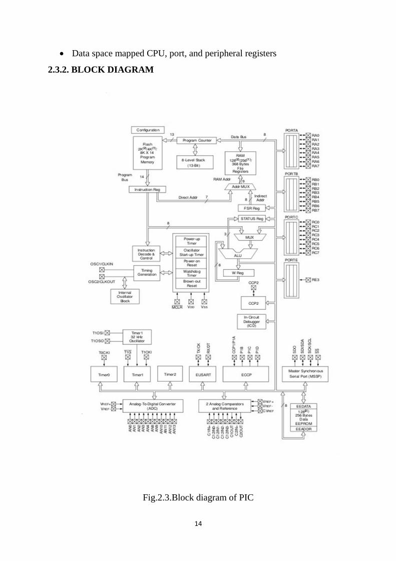
Data space mapped CPU, port, and peripheral registers
2.3.2. BLOCK DIAGRAM
Fig.2.3.Block diagram of PIC

15
2.3.3. PIN DIAGRAM
Fig.2.4. Pin diagram of PIC
Program Memory map and stack for the PIC16F887
The PIC16F887 has a 13-bit program counter capable of addressing an 8K x
14 (0000h-1FFFh) program memory space. This 8x14 memory space is broken
into 4 pages of 2k x 14 each. Page # Memory location within a page A12 A11
A10 A9 A8 A7 A6 A5 A4 A3 A2 A1 A0 Accessing a location above these
boundaries will cause a wrap-around within the first 8K x 14 space. The Reset

16
vector is at memory location 0000h and the interrupt vector is at memory
location 0004h.
2.3.4. STACK
PICs have a hardware call stack, which is used to save return addresses. The
hardware stack is not software accessible on earlier devices, but this changed
with the 18 series devices.
Hardware support for a general purpose parameter stack was lacking in early
series, but this greatly improved in the 18 series, making the 18 series
architecture more friendly to high level language compilers.
Fig.2.5 Stack
17
2.3.5. STATUS REGISTER
The STATUS register contains:
The arithmetic status of the ALU
The Reset status
The bank select bits for data memory (GPR and SFR)
It is recommended to use the BCF and BSF instructions for bit manipulation
and the MOVWF instruction for byte manipulation of the STATUS register.
register BSF
Move content of W register to the STATUS register.
2.3.6. I/O PORTS
The 16F887 provides various PORT I/O pins – These can be Used to interface
to the ―outside world‖. A total of 35 I/O pins are provided by the 16F887 and
are divided into various PORTS.
PORT: A B C D E
PINS: 8 8 8 8 3
The I/O pins can be individually programmed to be either inputs or outputs.
Many of the I/O pins are shared with another functionality. One needs to
program the 16F887 for the desired functionality.
PORTA and the TRISA Register
18
The RA4 pin is a Schmitt Trigger input and an open drain output. All other
RA port pins have TTL input levels and full CMOS output drivers. All pins
have data direction bits (TRIS registers) which can configure these pins as
output or input .Setting a TRISA register bit puts the corresponding output
driver in a hi-impedance mode. Clearing a bit in the TRISA register puts the
contents of the output latch on the selected pin(s).
The ANSEL register is used to configure the Input mode of an I/O pin to
analog. Setting the appropriate ANSEL bit high will cause all digital reads on
the pin to be read as ‗0‘ and allow analog functions on the pin to operate
correctly.
PORTB and the TRISB Register:
PORTB is an 8-bit wide bi-directional port. The corresponding data direction
register is TRISB. Setting a bit in the TRISB register puts the corresponding
output driver in a high-impedance input mode. Clearing a bit in the TRISB
register puts the contents of the output latch on the selected pins.
The ANSELH register is used to configure the input mode of a PORTB I/O
pin to analog. Setting the appropriate ANSELH bit high will cause all digital
reads on the pin to be read as ‗0‘ and allow analog functions on the pin to
operate correctly. All of the PORTB pins are individually configurable as an
interrupt-on-change pin. Control bits IOCB<7:0> enable or disable the interrupt
function for each pin. For enabled interrupt-on-change pins, the present value is
compared with the old value latched on the last read of PORTB to determine
which bits have changed or mismatched the old value. The ‗mismatch‘ outputs
of the last read are ORed together to set the PORTB Change Interrupt flag bit
(RBIF) in the INTCON register. A mismatch condition will continue to set flag
bit RBIF. Reading or writing PORTB will end the mismatch condition and
allow flag bit RBIF to be cleared.

19
PORTC and the TRISC Register:
PORTC is an 8-bit bi-directional port. Each pin is individually configurable
as an input or output through the TRISC register. PORTC pins have Schmitt
Trigger input buffers. When enabling peripheral functions, care should be taken
in defining TRIS bits for each PORTC pin. Some peripherals override the TRIS
bit to make a pin an output, while other peripherals override the TRIS bit to
make a pin an input.
PORTD and the TRISD Register:
PORTD is an 8-bit port with Schmitt Trigger input buffers. Each pin is
individually configurable as an input or output.
PORTE register:
PORTE provides a 3-bit wide, bidirectional port on RE0, RE1, and RE2
pins. The exception is RE3, which is input only and its TRISE bit will always
read as ‗1‘. The corresponding data direction register is TRISE (1 input, 0
output). Reading the PORTE register reads the status of the pins, whereas
writing to it will write to the PORT latch. The TRISE register controls the
PORTE pin output drivers, even when they are being used as analog inputs. The
user should ensure the bits in the TRISE register are maintained set when using
them as analog inputs. I/O pins configured as analog input always read ‗0‘. The
ANSEL register must be initialized to configure an analog channel as a digital
input. Pins configured as analog inputs will read ‗0‘.
2.3.7. INSTRUCTION SET
A PIC's instructions vary from about 35 instructions for the low-end PICs to
over 80 instructions for the high-end PICs. The instruction set includes
instructions to perform a variety of operations on registers directly, the

20
accumulator and a literal constant or the accumulator and a register, as well as
for conditional execution, and program branching.
To load a constant, it is necessary to load it into W before it can be moved into
another register. On the older cores, all register moves needed to pass through
W, but this changed on the "high end" cores.PIC cores have skip instructions
which are used for conditional execution and branching. The skip instructions
are: 'skip if bit set', and, 'skip if bit not set'. Because cores before PIC18 had
only unconditional branch instructions, conditional jumps are implemented by a
conditional skip (with the opposite condition) followed by an unconditional
branch. Skips are also of utility for conditional execution of any immediate
single following instruction.
PIC instructions fall into 5 classes: Operation on W with 8-bit immediate
("literal") operand. E.g. movlw (move literal to W), andlw (AND literal with
W). One instruction peculiar to the PIC is retlw, load immediate into W and
return, which is used with computed branches to produce lookup tables.
Operation with W and indexed register. The result can be written to either the
W register (e.g. addwfreg,w). or the selected register (e.g. addwfreg,f). The
latter are usedto perform conditional branches. The usual ALU status flags are
available in a numbered register so operations such as "branch on carry clear"
are possible. Control transfers. Other than the skip instructions previously
mentioned, there are only two:goto and call.
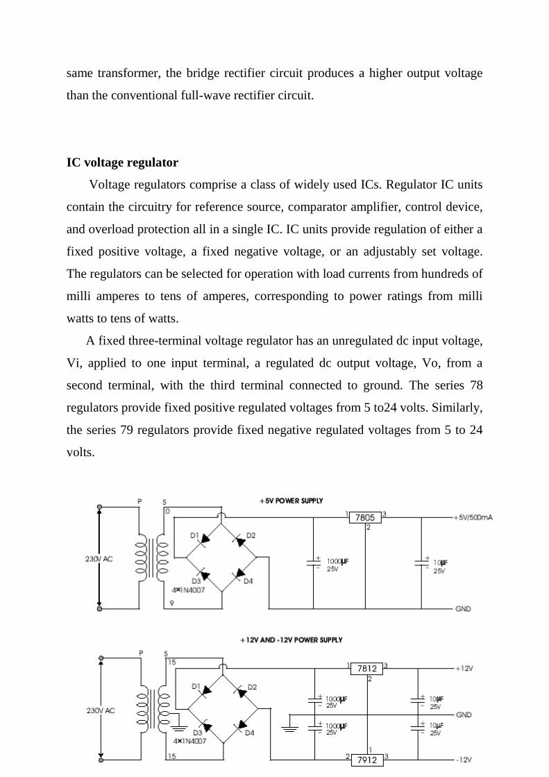
2.4. POWER SUPPLY UNIT
The ac voltage, typically 220V rms, is connected to a transformer, which
steps that ac voltage down to the level of the desired dc output. A diode rectifier
then provides a full-wave rectified voltage that is initially filtered by a simple
capacitor filter to produce a dc voltage. This resulting dc voltage usually has
some ripple or ac voltage variation.
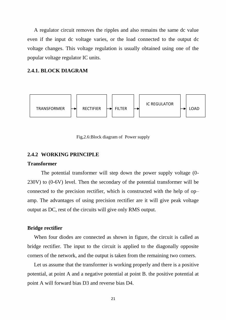
21
A regulator circuit removes the ripples and also remains the same dc value
even if the input dc voltage varies, or the load connected to the output dc
voltage changes. This voltage regulation is usually obtained using one of the
popular voltage regulator IC units.
2.4.1. BLOCK DIAGRAM
Fig,2.6:Block diagram of Power supply
2.4.2 WORKING PRINCIPLE
Transformer
The potential transformer will step down the power supply voltage (0-
230V) to (0-6V) level. Then the secondary of the potential transformer will be
connected to the precision rectifier, which is constructed with the help of op–
amp. The advantages of using precision rectifier are it will give peak voltage
output as DC, rest of the circuits will give only RMS output.
Bridge rectifier
When four diodes are connected as shown in figure, the circuit is called as
bridge rectifier. The input to the circuit is applied to the diagonally opposite
corners of the network, and the output is taken from the remaining two corners.
Let us assume that the transformer is working properly and there is a positive
potential, at point A and a negative potential at point B. the positive potential at
point A will forward bias D3 and reverse bias D4.
TRANSFORMER
RECTIFIER
FILTER
IC REGULATOR
LOAD
22
The negative potential at point B will forward bias D1 and reverse D2. At
this time D3 and D1 are forward biased and will allow current flow to pass
through them; D4 and D2 are reverse biased and will block current flow. The
path for current flow is from point B through D1, up through RL, through D3,
through the secondary of the transformer back to point B. this path is indicated
by the solid arrows. Waveforms (1) and (2) can be observed across D1 and D3.
One-half cycle later the polarity across the secondary of the transformer
reverse, forward biasing D2 and D4 and reverse biasing D1 and D3. Current
flow will now be from point A through D4, up through RL, through D2, through
the secondary of T1, and back to point A. This path is indicated by the broken
arrows. Waveforms (3) and (4) can be observed across D2 and D4. The current
flow through RL is always in the same direction. In flowing through RL this
current develops a voltage corresponding to that shown waveform (5). Since
current flows through the load (RL) during both half cycles of the applied
voltage, this bridge rectifier is a full-wave rectifier.
One advantage of a bridge rectifier over a conventional full-wave rectifier is
that with a given transformer the bridge rectifier produces a voltage output that
is nearly twice that of the conventional full-wave circuit.
This may be shown by assigning values to some of the components shown in
views A and B. assume that the same transformer is used in both circuits. The
peak voltage developed between points X and y is 1000 volts in both circuits. In
the conventional full-wave circuit shown—in view A, the peak voltage from the
center tap to either X or Y is 500 volts. Since only one diode can conduct at any
instant, the maximum voltage that can be rectified at any instant is 500 volts.
The maximum voltage that appears across the load resistor is nearly-but
never exceeds-500 v0lts, as result of the small voltage drop across the diode. In
the bridge rectifier shown in view B, the maximum voltage that can be rectified
is the full secondary voltage, which is 1000 volts. Therefore, the peak output
voltage across the load resistor is nearly 1000 volts. With both circuits using the
23
same transformer, the bridge rectifier circuit produces a higher output voltage
than the conventional full-wave rectifier circuit.
IC voltage regulator
Voltage regulators comprise a class of widely used ICs. Regulator IC units
contain the circuitry for reference source, comparator amplifier, control device,
and overload protection all in a single IC. IC units provide regulation of either a
fixed positive voltage, a fixed negative voltage, or an adjustably set voltage.
The regulators can be selected for operation with load currents from hundreds of
milli amperes to tens of amperes, corresponding to power ratings from milli
watts to tens of watts.
A fixed three-terminal voltage regulator has an unregulated dc input voltage,
Vi, applied to one input terminal, a regulated dc output voltage, Vo, from a
second terminal, with the third terminal connected to ground. The series 78
regulators provide fixed positive regulated voltages from 5 to24 volts. Similarly,
the series 79 regulators provide fixed negative regulated voltages from 5 to 24
volts.
24
Fig. 2.7: Circuit diagram of Power supply
2.5. RFID
Radio-frequency identification is the use of a wireless non-contact system
that uses radio-frequency electromagnetic fields to transfer data from a tag
attached to an object, for the purposes of automatic identification and tracking.
Some tags require no battery and are powered by the electromagnetic fields
used to read them. Others use a local power source and emit radio waves
(electromagnetic radiation at radio frequencies). The tag contains electronically
stored information which can be read from up to several meters (yards) away.
Unlike a bar code, the tag does not need to be within line of sight of the reader
and may be embedded in the tracked object.
2.5.1. RFID TAG
RFID tags are used in many industries. An RFID tag attached to an
automobile during production can be used to track its progress through the
assembly line. Pharmaceuticals can be tracked through warehouses. Livestock
and pets may have tags injected, allowing positive identification of the animal.
RFID identity cards can give employees access to locked areas of a building,
and RF transponders mounted in automobiles can be used to bill motorists for
access to toll roads or parking.
Since RFID tags can be attached to clothing, possessions, or even implanted
within people, the possibility of reading personally-linked information without
consent has raised privacy concerns

25
Design
A radio-frequency identification system uses tags, or labels attached to the
objects to be identified. Two-way radio transmitter-receivers called
interrogators or readers send a signal to the tag and read its response. The
readers generally transmit their observations to a computer system running
RFID software or RFID middleware.
The tag's information is stored electronically in a non-volatile memory. The
RFID tag includes a small RF transmitter and receiver. An RFID reader
transmits an encoded radio signal to interrogate the tag. The tag receives the
message and responds with its identification information. This may be only a
unique tag serial number, or may be product-related information such as a stock
number, lot or batch number, production date, or other specific information.
RFID tags can be either passive, active or battery assisted passive. An active
tag has an on-board battery and periodically transmits its ID signal. A battery
assisted passive (BAP) has a small battery on board and is activated when in the
presence of a RFID reader. A passive tag is cheaper and smaller because it has
no battery. Instead, the tag uses the radio energy transmitted by the reader as its
energy source. The interrogator must be close for RF field to be strong enough
to transfer sufficient power to the tag. Since tags have individual serial numbers,
the RFID system design can discriminate several tags that might be within the
range of the RFID reader and read them simultaneously.

26
Tags may either be read-only, having a factory-assigned serial number that is
used as a key into a database, or may be read/write, where object-specific data
can be written into the tag by the system user. Field programmable tags may be
write-once, read-multiple; "blank" tags may be written with an electronic
product code by the user.
RFID tags contain at least two parts: an integrated circuit for storing and
processing information, modulating and demodulating a radio-frequency (RF)
signal, collecting DC power from the incident reader signal, and other
specialized functions; and an antenna for receiving and transmitting the signal.
Fixed readers are set up to create a specific interrogation zone which can be
tightly controlled. This allows a highly defined reading area for when tags go in
and out of the interrogation zone. Mobile readers may be hand-held or mounted
on carts or vehicles.
Tag Chip
The tag's chip or integrated circuit (IC) delivers performance, memory and
extended features to the tag. The chip is pre-programmed with a tag identifier
(TID), a unique serial number assigned by the chip manufacturer, and includes a
memory bank to store the items' unique tracking identifier (called an electronic
product code or EPC).
Tag Antennas
Tag antennas collect energy and channel it to the chip to turn it on. Generally,
the larger the tag antenna's area, the more energy it will be able to collect and
channel toward the tag chip, and the further read range the tag will have.
There is no perfect antenna for all applications. It is the application that
defines the antenna specifications. Some tags might be optimized for a

27
particular frequency band, while others might be tuned for good performance
when attached to materials that may not normally work well for wireless
communication (certain liquids and metals, for example). Antennas can be made
from a variety of materials; they can be printed, etched, or stamped with
conductive ink, or even vapour deposited onto labels.
Tags that have only a single antenna are not as reliable as tags with multiple
antennas. With a single antenna, a tag's orientation can result in ―dead zones‖,
or areas on the tag where incoming signals cannot be easily harvested to provide
sufficient energy to power on the chip and communicate with the reader. A tag
with dual antennas is able to eliminate these dead zones and increase its
readability but requires a specialized chip.
2.5.2. RFID READERS
An RFID reader, also known as an interrogator, is a device that provides the
connection between the tag data and the enterprise system software that needs
the information. The reader communicates with tags that are within its field of
operation, performing any number of tasks including simple continuous
inventorying, filtering (searching for tags that meet certain criteria), writing (or
encoding) to selected tags, etc.
The reader uses an attached antenna to capture data from tags. It then passes
the data to a computer for processing. Just like RFID tags, there are many
different sizes and types of RFID readers. Readers can be affixed in a stationary
position in a store or factory, or integrated into a mobile device such as a
portable, handheld scanner. Readers can also be embedded in electronic
equipment or devices, and in vehicles.
Reader Antennas
28
RFID readers and reader antennas work together to read tags. Reader
antennas convert electrical current into electromagnetic waves that are then
radiated into space where they can be received by a tag antenna and converted
back to electrical current. Just like tag antennas, there is a large variety of reader
antennas and optimal antenna selection varies according to the solution's
specific application and environment.
The two most common antenna types are linear- and circular-polarized
antennas. Antennas that radiate linear electric fields have long ranges, and high
levels of power that enable their signals to penetrate through different materials
to read tags. Linear antennas are sensitive to tag orientation; depending on the
tag angle or placement, linear antennas can have a difficult time reading tags.
Conversely, antennas that radiate circular fields are less sensitive to orientation,
but are not able to deliver as much power as linear antennas.
Choice of antenna is also determined by the distance between the RFID
reader and the tags that it needs to read. This distance is called read range.
Reader antennas operate in either a "near-field" (short range) or "far-field" (long
range). In near-field applications, the read range is less than 30 cm and the
antenna uses magnetic coupling so the reader and tag can transfer power. In
near-field systems, the readability of the tags is not affected by the presence of
dielectrics such as water and metal in the field.
In far-field applications, the range between the tag and reader is greater than
30 cm and can be up to several tens of meters. Far-field antennas utilize
electromagnetic coupling and dielectrics can weaken communication between
the reader and tags.
2.6. RELAY
A relay is an electrically operated switch. Many relays used
an electromagnet to operate a switching mechanism mechanically, but other
29
operating principles are also used. Relays are used where it is necessary to
control a circuit by a low-power signal (with complete electrical isolation
between control and controlled circuits), or where several circuits must be
controlled by one signal. The first relays were used in long distance telegraph
circuits, repeating the signal coming in from one circuit and re-transmitting it to
another. Relays were used extensively in telephone exchanges and early
computers to perform logical operations.
A type of relay that can handle the high power required to directly drive an
electric motor is called a contactor. Solid-state relays control power circuits
with no moving parts, instead using a semiconductor device to perform
switching. Relays with calibrated operating characteristics and sometimes
multiple operating coils are used to protect electrical circuits from overload or
faults; in modern electric power systems these functions are performed by
digital instruments still called "protective relays".
2.6.1. RELAY DRIVER CRICUIT
The relay driver circuit is enabled certain time duration only, such
enable pulse is depended by delay programming of microcontroller, here darling
circuit has been two transistors made connection of cascade network, if input is
set to base of the first transistor, then that is turn on and emitter current of that
turn the another one. Hereby the circuit is closed through coil and second
transistor, now the energized coil is controls the contactors that are change the
normally open to close and normally closed to open connection. The enabled
signal is not essential after energized that coil because transistor collector
current maintains the transistors in saturation state continuously.
The induction effect may be affect the indication components and
another thing, so diode is connected across the coil which can prevents the
30
chopping effect the inverse magnitude of magnetic field shorted across from
coil.
2.7. GSM
GSM is one of the widely used mobile standards. GSM is Global System
for Mobile Communication. As the name specifies, it enables the mobile users
to interact all over the world at any time. GSM was actually designed to be
platform independent. Because GSM provides a common standard, cellular
subscribers can use their telephones over the entire GSM area which includes all
the countries around the world where the GSM system is used. In addition, the
GSM provides user services such as high-speed data communication, facsimile
and a Short Message Service (SMS). The GSM technical specifications are
also designed to work with other standards as it guarantees standard interfaces.
Finally a key aspect of GSM is that the specifications are open ended and can be
built upon to meet the future requirements.

31
2.7.1. MOBILE STANDARDS
The primary purpose of a standard for mobile communication is to specify
how mobile phone calls are to be handled by a mobile network.
This specification includes the following.
The signals to be transmitted and received by the mobile phone.
The format of these signals.
The interaction of the network nodes.
The basic network services which should be available to mobile
subscribers.

32
The basic network structure.
2.7.2. SMS
SMS stands for Short Message Service. It is a technology that enables the
sending and receiving messages between the mobile phones. The SMS was
included in the GSM (Global System for Mobile Communication) standards
right at the beginning. Later it was ported to wireless technologies like CDMA
and TDMA. The GSM and SMS standards were originally developed by the
ETSI. ETSI is the abbreviation for European Telecommunications Standards
Institute. Now the 3GPP (Third Generation Partnership Project) is
responsible for the development of GSM and SMS standards.
As suggested by the name ―Short Message Service” the amount of data that
can be supported by an SMS is very limited. One SMS message can contain at
most 140 bytes.
2.7.3. ADVANTAGES OF GSM
SMS is a great success all over the world. SMS messaging is one of the most
important revenues of the wireless carriers. The number of messages exchanged
every day is very enormous.
Some of the reasons behind the popularity of the SMS are described below.
SMS messages can be sent and read at any time
Nowadays most of the persons have a mobile phone and carries it most of the
time. With a mobile phone, we can send and read messages at any time and at
any place be it at the home, bus, office etc.
33
SMS messages can be sent to an offline mobile phone
Unlike a phone call we can send the message to our friend when he / she has
switched of the mobile phone or he /she is in the place where the wireless signal
is temporarily unavailable. The SMS system of the mobile network operator
will store the message and later send it to our friend.
SMS messages are less disturbing
Unlike a phone call, we need not read or reply an SMS message immediately.
Besides reading and writing the messages do not make any noise. We need not
attend the messages urgently as we do in case of an urgent phone call.
SMS messages can be exchanged over different wireless carriers
SMS technology is a very mature technology. Not only can we exchange the
messages with the mobile users of same wireless carriers but also with the
mobile users of different wireless carriers. So the 100% GSM phones support
Short Message Service.
2.7.4. APPLICATIONS OF GSM
There are many different kinds of SMS applications on the market today and
many others can be developed. Applications in which the SMS messaging can
be utilized are virtually unlimited. Some of the applications are described
below.
Person-to-Person Text Messaging
Person to person text messaging is the most commonly used SMS application.
Here, a person types a text message to his friend using the keypad of his mobile
phone and then inputs the mobile phone number of the recipient and clicks the
Send option on the screen to send the message out. When the recipient mobile

34
phone receives the sent text message, it will notify the user by giving out a
sound or a vibration. The recipient can then read and respond either
immediately or at any time later.
Provision of information
It is another popular application of the SMS technology. Many content
providers make use of the SMS text messages to send the information such as
news, weather report and financial data to their subscribers. Many of these
information services are not free.
Downloading
SMS can be used as a transport medium of wireless downloads since it carries
binary data. Objects such as pictures, wallpapers, and logos can be encoded in
one or more SMS messages depending upon the object‘s size. Like information
services wireless download services are also not free.
Alerts and Notifications
SMS is a very suitable technology for delivering alerts and notifications of
important events. This is because of two reasons:
A mobile phone is a device that is carried by its owner most of the
time. Whenever an SMS text message is received, the mobile phone
will notify you by giving out a sound or by vibrating. You can check
what the SMS text message contains immediately.
SMS technology allows the "push" of information. This is different
from the "pull" model where a device has to poll the server regularly
in order to check whether there is any new information. The "pull"
model is less suitable for alert and notification applications, since it
wastes bandwidth and increases server load.
2.8. SERIAL COMMUNICATION
35
Serial data is any data that is sent one bit at a time using a single electrical
signal. In contrast, parallel data is sent 8, 16, 32, or even 64 bits at a time using
a signal line for each bit. Data that is sent without the use of a master clock is
said to be asynchronous serial data.
2.8.1. RS 232
Several communications standards exist for the transfer of asynchronous
serial data. Common PC's transfer data using the EIA RS-232C (also known as
V.28 or V.24). Updated versions of this standard include RS-232D and
EIA/TIA-232E, but most literature still refers to the RS-232C or RS-232
standard. The baud rate for a serial connection is the number of bits that are
transmitted per second. It is specified in bits/second or baud. For example, a 110
baud serial link transfers 110 bits of data per second.
Data transfer rate
The rate of data transfer in serial data communication is stated in bps(bits per
second). Another widely used terminology for bps is baud rate. Baud rate is
defined as the number of signal changes per second. In modems, there are
occasions when a single change of signal transfers several bits of data. As far as
the conductor wire is concerned, the baud rate and bps are the same. It must be
noted that in asynchronous serial data communication, the baud rate is generally
limited to 100,000 bps.
RS232 Standards
To allow compatibility among data communication equipment made by
various manufactures, an interfacing standard called RS232 was set by the
Electronics Industries Association (EIA) in 1960. RS232 is the most widely
used serial I/O interfacing standard.
2.8.2. MAX 232
36
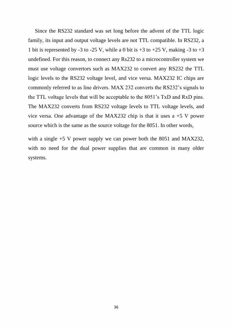
Since the RS232 standard was set long before the advent of the TTL logic
family, its input and output voltage levels are not TTL compatible. In RS232, a
1 bit is represented by -3 to -25 V, while a 0 bit is +3 to +25 V, making -3 to +3
undefined. For this reason, to connect any Rs232 to a microcontroller system we
must use voltage convertors such as MAX232 to convert any RS232 the TTL
logic levels to the RS232 voltage level, and vice versa. MAX232 IC chips are
commonly referred to as line drivers. MAX 232 converts the RS232‘s signals to
the TTL voltage levels that will be acceptable to the 8051‘s TxD and RxD pins.
The MAX232 converts from RS232 voltage levels to TTL voltage levels, and
vice versa. One advantage of the MAX232 chip is that it uses a +5 V power
source which is the same as the source voltage for the 8051. In other words,
with a single +5 V power supply we can power both the 8051 and MAX232,
with no need for the dual power supplies that are common in many older
systems.
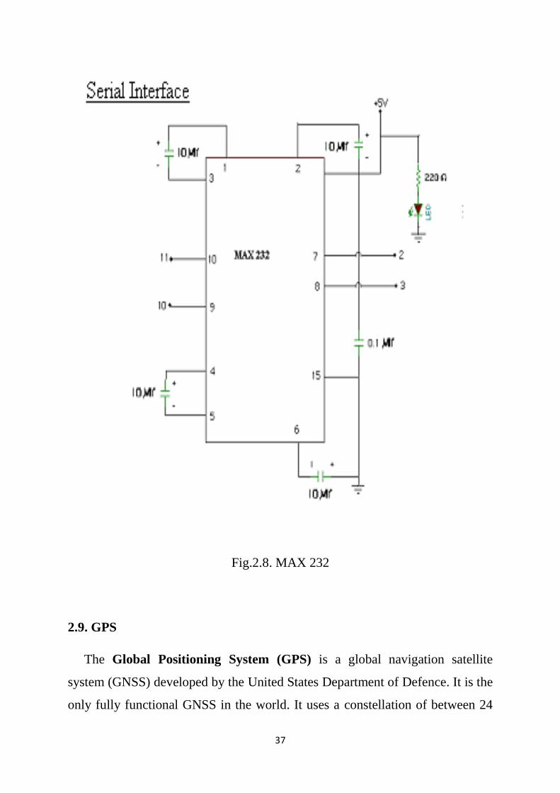
37
Fig.2.8. MAX 232
2.9. GPS
The Global Positioning System (GPS) is a global navigation satellite
system (GNSS) developed by the United States Department of Defence. It is the
only fully functional GNSS in the world. It uses a constellation of between 24
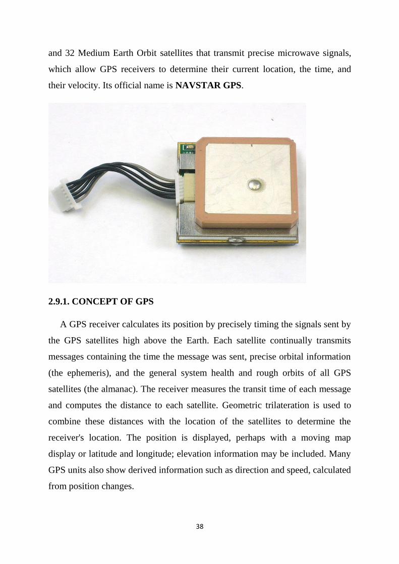
38
and 32 Medium Earth Orbit satellites that transmit precise microwave signals,
which allow GPS receivers to determine their current location, the time, and
their velocity. Its official name is NAVSTAR GPS.
2.9.1. CONCEPT OF GPS
A GPS receiver calculates its position by precisely timing the signals sent by
the GPS satellites high above the Earth. Each satellite continually transmits
messages containing the time the message was sent, precise orbital information
(the ephemeris), and the general system health and rough orbits of all GPS
satellites (the almanac). The receiver measures the transit time of each message
and computes the distance to each satellite. Geometric trilateration is used to
combine these distances with the location of the satellites to determine the
receiver's location. The position is displayed, perhaps with a moving map
display or latitude and longitude; elevation information may be included. Many
GPS units also show derived information such as direction and speed, calculated
from position changes.

39
It might seem three satellites are enough to solve for position, since space
has three dimensions. However a very small clock error multiplied by the very
large speed of light at which satellite signals propagate—results in a large
positional error.
2.9.2. POSITION CALCULATION
To provide an introductory description of how a GPS receiver works,
measurement errors will be ignored in this section. Using messages received
from a minimum of four visible satellites, a GPS receiver is able to determine
the satellite positions and time sent. The x, y, and z components of position and
the time sent are designated as where the subscript i is the satellite number and
has the value 1, 2, 3, or 4. Knowing the indicated time the message was
received, the GPS receiver can compute the indicated transit time, of the
message. Assuming the message travelled at the speed of light, c, the distance
travelled, can be computed as. Knowing the distance from GPS receiver to a
satellite and the position of a satellite implies that the GPS receiver is on the
surface of a sphere cantered at the position of a satellite. Thus we know that the
indicated position of the GPS receiver is at or near the intersection of the
surfaces of four spheres. In the ideal case of no errors, the GPS receiver will be
at an intersection of the surfaces of four spheres. The surfaces of two spheres, if
they intersect in more than one point, intersect in a circle. A figure, Two Sphere
Surfaces Intersecting in a Circle, is shown below.
Two sphere surfaces intersecting in a circle
The article, trilateration, shows mathematically that two spheres intersecting
in more than one point intersect in a circle.

40
A circle and sphere surface in most cases of practical interest intersects at
two points, although it is conceivable that they could intersect at one point—or
not at all. Another figure, Surface of Sphere Intersecting a Circle (not disk) at
Two Points, shows this intersection. The two intersections are marked with dots.
Again trilateration clearly shows this mathematically. The correct position of
the GPS receiver is the intersection that is closest to the surface of the earth for
automobiles and other near-Earth vehicles. The correct position of the GPS
receiver is also the intersection which is closest to the surface of the sphere
corresponding to the fourth satellite. (The two intersections are symmetrical
with respect to the plane containing the three satellites. If the three satellites are
not in the same orbital plane, the plane containing the three satellites will not be
a vertical plane passing through the centre of the Earth. In this case one of the
intersections will be closer to the earth than the other. The near-Earth
intersection will be the correct position for the case of a near-Earth vehicle. The
intersection which is farthest from Earth may be the correct position for space
vehicles.
A TYPICAL RECEIVER WITH INTEGRATED ANTENNA
Many GPS receivers can relay position data to a PC or other device using the
NMEA 0183 protocol, or the newer and less widely used NMEA 2000.
Although these protocols are officially defined by the NMEA, references to
these protocols have been compiled from public records, allowing open source
tools like GPS to read the protocol without violating intellectual property laws.

41
Other proprietary protocols exist as well, such as the SiRF and MTK protocols.
Receivers can interface with other devices using methods including a serial
connection, USB or Bluetooth.
Broadcast Signal
Each GPS satellite continuously broadcasts a Navigation Message at 50
bit/s giving the time-of-week, GPS week number and satellite health
information (all transmitted in the first part of the message), an ephemeris
(transmitted in the second part of the message) and an almanac (later part of the
message). The messages are sent in frames, each taking 30 seconds to transmit
1500 bits.
Transmission of each 30 second frame begins precisely on the minute and
half minute as indicated by the satellite's atomic clock according to Satellite
message format. Each frame contains 5 sub frames of length 6 seconds and with
300 bits. Each sub frame contains 10 words of 30 bits with length 0.6 seconds
each.
Words 1 and 2 of every sub frame have the same type of data. The first word
is the telemetry word which indicates the beginning of a sub frame and is used
by the receiver to synch with the navigation message. The second word is the
HOW or handover word and it contains timing information which enables the
receiver to identify the sub frame and provides the time the next sub frame was
sent.
Words 3 through 10 of sub frame 1 contain data describing the satellite clock
and its relationship to GPS time. Words 3 through 10 of sub frames 2 and 3,
contain the ephemeris data, giving the satellite's own precise orbit. The
ephemeris is updated every 2 hours and is generally valid for 4 hours, with
provisions for updates every 6 hours or longer in non-nominal conditions. The
time needed to acquire the ephemeris is becoming a significant element of the

42
delay to first position fix, because, as the hardware becomes more capable, the
time to lock onto the satellite signals shrinks, but the ephemeris data requires 30
seconds (worst case) before it is received, due to the low data transmission rate.
2.10. LCD DISPLAY
Liquid crystal cell displays (LCDs) are used in similar applications where
LEDs are used. These applications are display of display of numeric and
alphanumeric characters in dot matrix and segmental displays.
LCDs are of two types
I. Dynamic scattering type
II. Field effect type
The construction of a dynamic scattering liquid crystal cell. The liquid
crystal material may be one of the several components, which exhibit optical
properties of a crystal though they remain in liquid form. Liquid crystal is
layered between glass sheets with transparent electrodes deposited on the inside
faces.
When a potential is applied across the cell, charge carriers flowing through
the liquid disrupt the molecular alignment and produce turbulence. When the
liquid is not activated, it is transparent. When the liquid is activated the
molecular turbulence causes light to be scattered in all directions and the cell
appease to be bright. This phenomenon is called dynamic scattering.
The construction of a field effect liquid crystal display is similar to that of
the dynamic scattering type, with the exception that two thin polarizing optical
filters are placed at the inside of each glass sheet. The liquid crystal material in
the field effect cell is also of different type from employed in the dynamic

43
scattering cell. The material used is twisted nemayic type and actually twists the
light passing through the cell when the latter is not energised.
Liquid crystal cells are of two types:
i. Transmittive type
ii. Reflective type
In the transmittive type cell, both glass sheets are transparent, so that light
from a rear source is scattered in the forward direction when the cell is
activated.
In reflective type cell has a reflecting surface on one side of glass sheets.
The incident light on the front surface of the cell is dynamically scattered by an
activated cell. Both types of cells appear quite bright when activated even under
ambient light conditions.
The liquid crystals are light reflectors are transmitters and therefore they
consume small amounts of energy (unlike light generators). The seven segment
display, the current is about 25micro Amps for dynamic scattering cells and
300micro amps for field effect cells. Unlike LEDs which can work on d.c. the
LCDs require a.c. voltage supply. A typical voltage supply to dynamic
scattering LCD is 30v peak to peak with 50 Hz.
2.10.1. FEATURES OF LCD
1. Polarizing filter film with a vertical axis to polarize light as it enters.
2. Glass substrate with ITO electrodes. The shapes of these electrodes will
determine the shapes that will appear when the LCD is turned ON.
Vertical ridges etched on the surface are smooth.
3. Twisted nematic liquid crystal.
4. Glass substrate with common electrode film (ITO) with horizontal ridges
to line up with the horizontal filter.

44
5. Polarizing filter film with a horizontal axis to block/pass light.
6. Reflective surface to send light back to viewer. (In a backlit LCD, this
layer is replaced with a light source.)
A liquid crystal display (LCD) is a flat panel display, electronic visual
display, video display that uses the light modulating properties of liquid crystals
(LCs). LCs don‘t emit light directly.
They are used in a wide range of applications, including computer monitors,
television, instrument panels, aircraft cockpit displays, signage, etc. They are
common in consumer devices such as video players, gaming devices, clocks,
watches, calculators, and telephones. LCDs have displaced cathode ray tube
(CRT) displays in most applications. They are usually more compact,
lightweight, portable, less expensive, more reliable, and easier on the eyes. They
are available in a wider range of screen sizes than CRT and plasma displays,
and since they do not use phosphors, they cannot suffer image burn-in.
LCDs are more energy efficient and offer safer disposal than CRTs. Its low
electrical power consumption enables it to be used in battery-powered electronic
equipment. It is an electronically modulated optical device made up of any
number of segments filled with liquid crystals and arrayed in front of a light
source (backlight) or reflector to produce images in color or monochrome. The
most flexible ones use an array of small pixels. The earliest discovery leading to
the development of LCD technology, the discovery of liquid crystals, dates
from 1888. By 2008, worldwide sales of televisions with LCD screens had
surpassed the sale of CRT units.

45
2.10.2. PIN DIAGRAM
Fig.2.9. LCD diagram
PIN NO SYMBOL FUNCTION
1 Vss Ground terminal of
Module
2 Vdd Supply terminal of
Module, +
5v
3 Vo Power supply for
liquid crystal drive
4 RS Register select
RS=0…Instruction
register
RS=1…Data register
46
2.10.3. ADVANTAGES
1. Consume much lesser energy (i.e. low power) when compared to
LEDs.
2. Utilizes the light available outside and no generation of light.
3. Since very thin layer of liquid crystal is used, more suitable to act as
display elements (in digital watches, pocket calculators, ect.)
4. Since reflectivity is highly sensitive to temperature, used as
temperature measuring sensor.
5. Very cheap.
2.10.4. APPLICATIONS
1. Watches
2. Fax & Copy machines & Calculators

47
3. SOFTWARE DESCRIPTION
3.1. PICkit Tool
Fig.3.1. PICkit 1
PICkit is a family of programmers for PIC microcontrollers made by
Microchip Technology. They are used to program and debug microcontrollers,
as well as program EEPROM. Some models also feature logic analyzer and
serial communications (UART) tool.
The people who develop open-source software for the PICkit use a mailing list
for collaboration.
PICkit 1
The PICkit 1 — introduced on March 31, 2003 for US $36 — was a
rudimentary USB programmer for PIC microcontrollers, produced by
Microchip Technology, the manufacturers of the PIC series of microcontrollers.
It was integrated into a demo board featuring 8 LEDs, a switch, and a
potentiometer. Its default program (explained in the documentation) rotates the
48
LEDs in series. The light display's direction and speed of rotation can be
changed with the button and potentiometer on the PICkit board.
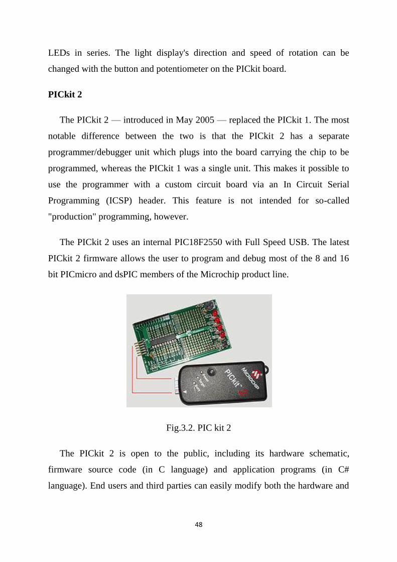
PICkit 2
The PICkit 2 — introduced in May 2005 — replaced the PICkit 1. The most
notable difference between the two is that the PICkit 2 has a separate
programmer/debugger unit which plugs into the board carrying the chip to be
programmed, whereas the PICkit 1 was a single unit. This makes it possible to
use the programmer with a custom circuit board via an In Circuit Serial
Programming (ICSP) header. This feature is not intended for so-called
"production" programming, however.
The PICkit 2 uses an internal PIC18F2550 with Full Speed USB. The latest
PICkit 2 firmware allows the user to program and debug most of the 8 and 16
bit PICmicro and dsPIC members of the Microchip product line.
Fig.3.2. PIC kit 2
The PICkit 2 is open to the public, including its hardware schematic,
firmware source code (in C language) and application programs (in C#
language). End users and third parties can easily modify both the hardware and

49
software for enhanced features. e.g. GNU/Linux version of PICKit 2 application
software, DOS style CMD support, etc.
The PICkit 2 has a programmer-to-go (PTG) feature, which can download the
hex file and programming instructions into on-board memory (128K byte I2C
EEPROM or 256K byte I2C EEPROM), so that no PC is required at the end
application.
The Microchip version of PICkit 2 has a standard 128K byte memory. 256K
byte memory can be achieved by modifying the hardware or from third party.
Additionally, a 500 kHz three-channel logic analyser and a UART tool are
built into the PICKit 2. These features are missing from the PICkit 3.
Since release of V2.61, PICkit 2 PC software now support maximum 4M
bytes of memory for programmer-to-go feature. This modification makes the
PICKit 2 support 8x more memory than the PICKit 3. This enhancement has
been contributed by Au Group Electronics and the PICkit 2 firmware is also
reported to be submitted to Microchip PICkit 2 team in the middle of March
2009. Hopefully this enhancement will be integrated into future firmware
releases too.
PICkit 3
Microchip has gone on to manufacture the PICkit 3, a variation of the
PICkit 2 with the same form factor and a new translucent case. It features a
faster 16-bit PIC24F processor and a wider voltage regulation range. There are
some complaints of it not being as reliable as the Pickit 2.

50
Fig.3.3. PIC kit 3
Both PICkit 2 and PICkit 3 have internal, switch-mode voltage regulators.
This allows them, in the case of the PICkit 2, to generate voltages from 2.5 to 5
volts, or in the case of the PICkit 3, 2.5 to 5.5 volts, from 5V USB, at around
100mA. Both have options for calibrating the output with a multi meter, for
increased accuracy. Additionally, for some PICs, the MCLR programming
voltage can be generated, at around 13-14 volts. This voltage is required to
reprogram the flash memory.
3.2. MPLAB IDE
COMPONENTS OF MPLAB IDE
The MPLAB IDE has both built-in components and plug-in modules to
configure the system for a variety of software and hardware tools.
Project Manager
The project manager provides integration and communication between the
IDE and the language tools.
Editor
The editor is a full-featured programmer's text editor that also serves as a
window into the debugger.

51
Assembler/Linker and Language Tools
The assembler can be used stand-alone to assemble a single file, or can be
used with the linker to build a project from separate source files, libraries and
recompiled objects. The linker is responsible for positioning the compiled code
into memory areas of the target microcontroller.
Debugger
The Microchip debugger allows breakpoints, single stepping, watch
windows and all the features of a modern debugger for the MPLAB IDE. It
works in conjunction with the editor to reference information from the target
being debugged back to the source code.
Execution Engines
There are software simulators in MPLAB IDE for all PIC micro MCU and
dsPIC DSC devices. These simulators use the PC to simulate the instructions
and some peripheral functions of the PIC micro MCU and dsPIC DSC devices.
Optional in-circuit emulators and in-circuit debuggers are also available to test
code as it runs in the applications hardware.
The MPLAB IDE provides the ability to
Create and edit source code using the built-in editor.
Assemble, compile and link source code.
Debug the executable logic by watching program flow with the built-in
simulator or in real time with in-circuit emulators or in-circuit debuggers.
Make timing measurements with the simulator or emulator.
View variables in Watch windows.
Program firmware into devices with device programmers

52
The following minimum configuration is required to run MPLAB IDE:
• PC compatible Pentium class system
• Microsoft Windows 3.1x, Windows 95/98, and above
• 16 MB memory (32 MB recommended)
• 45 MB of hard disk space
3.3. EMBEDDED C
Embedded C uses most of the syntax and semantics of standard C, e.g.,
main() function, variable definition, data type declaration, conditional
statements (if, switch, case), loops (while, for), functions, arrays and strings,
structures and union, bit operations, macros, etc.
Necessity
During infancy years of microprocessor based systems, programs were
developed using assemblers and fused into the EPROMs. There used to be no
mechanism to find what the program was doing. LEDs, switches, etc. were used
to check for correct execution of the program. Some ‗very fortunate‘ developers
had In-Circuit Emulator's (ICE's), but they were too costly and were not quite
reliable as well. As time progressed, use of microprocessor-specific assembly-
only as the programming language reduced and embedded systems moved onto
C as the embedded programming language of choice. C is the most widely used
programming language for embedded processors/controllers. Assembly is also
used but mainly to implement those portions of the code where very high timing
accuracy, code size efficiency, etc. are prime requirements.
As assembly language programs are specific to a processor, assembly
language didn‘t offer portability across systems. To overcome this
disadvantage, several high level languages, including C, came up. Some other

53
languages like PLM, Modula-2, Pascal, etc. also came but couldn‘t find wide
acceptance. Amongst those, C got wide acceptance for not only embedded
systems, but also for desktop applications. Even though C might have lost its
sheen as a mainstream language for general purpose applications, it still has a
strong-hold in embedded programming. Due to the wide acceptance of C in
embedded systems, various kinds of support tools like compilers & cross-
compilers, ICE, etc. came up, and all this facilitated development of embedded
systems using C. Assembly language seems to be an obvious choice for
programming embedded devices. However, use of assembly language is
restricted to developing efficient codes in terms of size and speed. Also,
assembly codes lead to higher software development costs and code portability
is not there. Developing small codes are not much of a problem, but large
programs/projects become increasingly difficult to manage in assembly
language. Finding good assembly programmers has also become difficult.
Hence high level languages are preferred for embedded systems programming.
Advantages
It is small and simpler to learn, understand, program and debug.
Compared to assembly language, C code written is more reliable and
scalable, more portable between different platforms.
C compilers are available for almost all embedded devices in use today,
and there is a large pool of experienced C programmers.
Unlike assembly, C has advantage of processor-independence and is not
specific to any particular microprocessor/microcontroller or any system.
This makes it convenient for a user to develop programs that can run on
most of the systems.
As C combines functionality of assembly language and features of high
level languages, C is treated as a ‗middle-level computer language‘ or
‗high level assembly language‘.

54
It is fairly efficient.
It supports access to I/O and provides ease of management of large
embedded projects.
Java is also used in many embedded systems but Java programs require
the Java Virtual Machine (JVM), which consumes a lot of resources.
Hence it is not used for smaller embedded devices.
In Embedded we need read/write data on given address, so in C its Easy
to access and modify, because of its pointer concept.
Other High-level programming language like Pascal, FORTRAN also
provides some of the advantages.

55
4. WORKING
When the engine is ignited, the school bus starts to move and the module
gets triggered on with the help of a power supply unit. The power supply unit
has a transformer (step-down), bridge rectifier and LM7805 IC. The transformer
is used to convert 230V AC power supply to 12V AC supply. The bridge
rectifier converts this AC power supply to DC voltage. IC LM7805 is used to
prevent the controller from the damage in case of any voltage fluctuations.
From this unit, the power supply is given to all other units. There is a provision
for noise filtering using ceramic capacitors.
There are two relays namely relay 1 and relay 2. Relay 1 has a connection
with RFID and GSM. Relay 2 is connected with both GPS and GSM. GSM is
serially connected to the PIC micro-controller with the help of an UART. As
GSM works on AC supply, the DC supply from the PIC microcontroller is
converted into the AC supply with the help of UART. Whenever the valid tag is
read, the reader is connected to the relay 1 and the connection between the relay
2 and GPS will be disconnected. As GPS is a continuous monitoring system the
last tracked location is sent to the microcontroller. The count of the number of
students getting into the bus is displayed on the LCD through the PIC micro
controller. Here we have used 16x2 LCD displays which has two rows and it
has 16 characters in each row which is used to display the student information
stored in the RFID tag. For the entry of each student into the bus, the student‘s
status with the location is sent to the respective parents with the help of GSM.
In the same way how the message reaches the parent when the student boarded
the bus, the message again reaches the parents even when they get down from
the bus. The student attendance is recorded in the controller which can be sent
to the management manually.
56
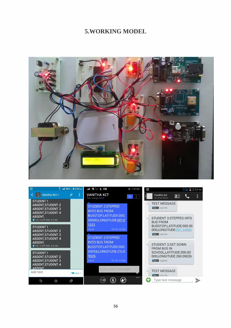
5.WORKING MODEL

57
6. CONCLUSION
This project presents a system to monitor pick-up/drop-off of school children
to enhance the safety of children during the daily transportation from and to
school. The system consists of two main units, a bus unit and a school unit. The
bus unit the system is used to detect when a child boards or leaves the bus. This
information is communicated to the school unit that identifies which of the
children did not board or leave the bus and issues an alert message accordingly.
The system has a developed web-based database-driven application that
facilities its management and provides useful information about the children to
authorized personal. A complete prototype of the proposed system was
implemented and tested to validate the system functionality. The results show
that the system is promising for daily transportation safety.
58
REFERENCES
[1] Khaled Shaaban et.al ―5Smart Tracking System for School Buses
Using Passive RFID Technology to Enhance Child Safety‖ , Journal of Traffic
and Logistics Engineering, Vol 1( 2), pages: 191-196, Dec 2013.
[2] Seong-eun Yoo, Poh Kit Chong, Daeyoung Kim, ―School Zone Safety
System Based on Wireless Sensor Network‖, Journal of Sensors, Vol 9, Pages
5968-5988, July 2009.
[3] G. Bharathi, L.Rammurthy , ― Implementation of children tracking system
using ARM7 microcontroller‖, International Journal of Industrial Electronics
and Electrical Engineering, Volume-2(12): pages 18-21, Dec.-2014.
[4] V.SivaSankaran et.al , ― Advanced embedded system assisted GSM and
RFID based smart school management system‖ , International journal of
advanced research in electrical , Electronics and Instrumentation Engineering,
Vol 2(7): pages 3124-3128, July 2013.
[5] M. Navya, et.al , ― Android based children tracking system using voice
recognition‖, International journal of Computer science and information
technology,Vol 4 (1): pages 229-235, Jan 2015.
[6] Khaled Shaaban et.al, ―Smart Tracking System for School Buses Using
Passive RFID Technology to Enhance Child Safety ― , Journal of Traffic and
Logistics Engineering, Vol 1( 2): pages 191-196, Dec 2013.
[7] J.Saranya , J.Selvakumar, ―Implementation of Children Tracking System on
Android Mobile Terminals ― , International conference on Communication and
Signal Processing, April 3-5, 2013, India 9