bus and accelerator
TRANSCRIPT

Bus, DMA and AcceleratorChixiao Chen

Announcement
• HW 2 is online
• We will not have classes next week.
• Complete HW2 next week.

Last time Review
• Memory Hierarchy : Using cache instead of direct access on Memory

Outline
• IO Devices
• Bus Introduction (AMBA and AXI4)
• DMA
• Accelerator
• NOC

A Computer is Useless without I/O
• Storage (DRAM/SSD)
• Interface(keyboard, mouse, downloader)
• Networks with other processors
How to control/access them ?

Treat all devices as memory
• A memory-mapped interface• Processor can write & read to control registers to tell the device what to do
• Processor can write & read data to the device
• The "device driver" runs in the operating system • Provides a device independent abstraction to the rest of the OS
• And user programs have to ask the OS for permission
• Programmed I/O: • The CPU is responsible to transfer data to the devices as well as commands

Reading register bits with MMIO
• How?• Let’s say that red, green, and blue pushbuttons are mapped to memory
address 0xB0000003 at bits 0, 1, and 2, respectively
• When pushed, we will read a ‘1’ from the corresponding bit
• When released, we will read a ‘0’ from the corresponding bit
Address \ Bit 31 24 23 16 15 8 7 210
0xB0000003-------- -------- -------- -----

Writing register bits with MMIO
• How?• Let’s say that red, green, and blue LEDs are mapped to
memory address 0xB0000004 at bits 0, 1, and 2, respectively
• Writing a ‘1’ (‘0’) to the corresponding bit turns on (off) the LED
Address \ Bit 31 24 23 16 15 8 7 210
0xB0000004-------- -------- -------- -----
• When updating (set/clear) bits, must preserve remaining contents
• Use bitmask to select target bits for manipulation, e.g.
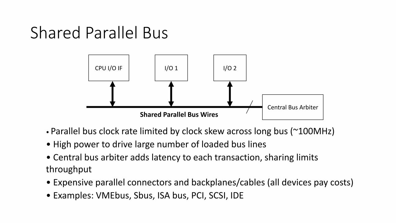
Shared Parallel Bus
CPU I/O IF I/O 1 I/O 2
Central Bus ArbiterShared Parallel Bus Wires
• Parallel bus clock rate limited by clock skew across long bus (~100MHz)
• High power to drive large number of loaded bus lines
• Central bus arbiter adds latency to each transaction, sharing limits throughput
• Expensive parallel connectors and backplanes/cables (all devices pay costs)
• Examples: VMEbus, Sbus, ISA bus, PCI, SCSI, IDE

Simple I/O Bus Structure
• Some range of physical addresses map to I/O bus devices
• I/O bus bridge reduces loading on critical CPU-DRAM bus
• Devices can be “slaves”, only responding to I/O bus requests
• Devices can be “masters”, initiating I/O bus transfers
10
CPU
Caches
DRAM
I/O Bus Bridge
Memory Bus
I/O Bus
I/O Device
#1
I/O Device
#2
I/O Device
#3
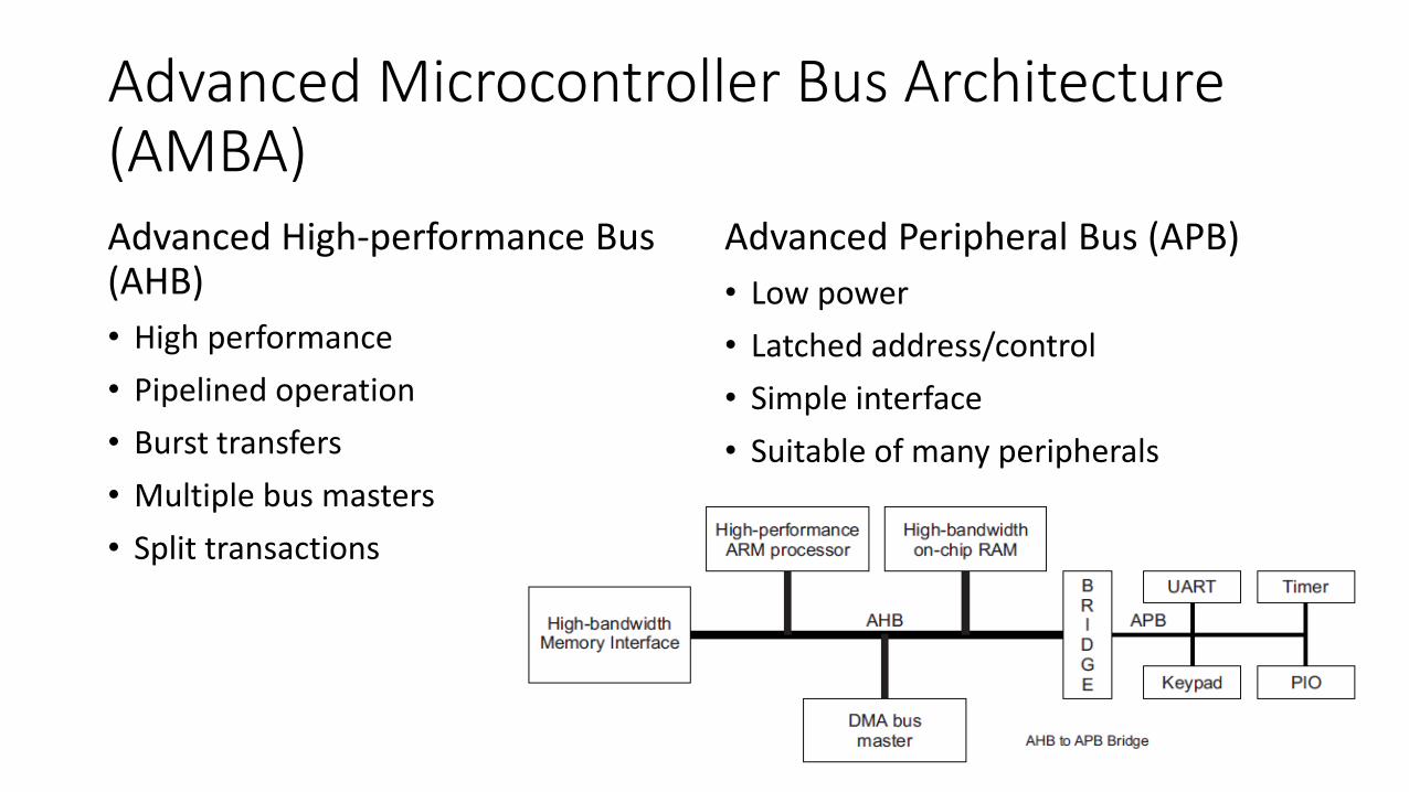
Advanced Microcontroller Bus Architecture (AMBA)Advanced High-performance Bus (AHB)
• High performance
• Pipelined operation
• Burst transfers
• Multiple bus masters
• Split transactions
Advanced Peripheral Bus (APB)
• Low power
• Latched address/control
• Simple interface
• Suitable of many peripherals

AHB-lite Master / Slave Interface
• Global signals : • HCLK
• HRESETn
• Master out/slave in• HADDR (address)
• HWDATA (write data)
• Control
• HWRITE
• HSIZE
• HBURST
• HPROT
• HTRANS
• HMASTLOCK
• Slave out/master in• HRDATA (read data)
• HREADY
• HRESP

AMBA Advanced eXtensible Interface 4 (AXI4)
• The fourth generation of AMBA interface defined in the AMBA 4 specification, targeted at high performance, high clock frequency systems. Introduced by ARM in 2010.
• AXI 4 use 5 channels!
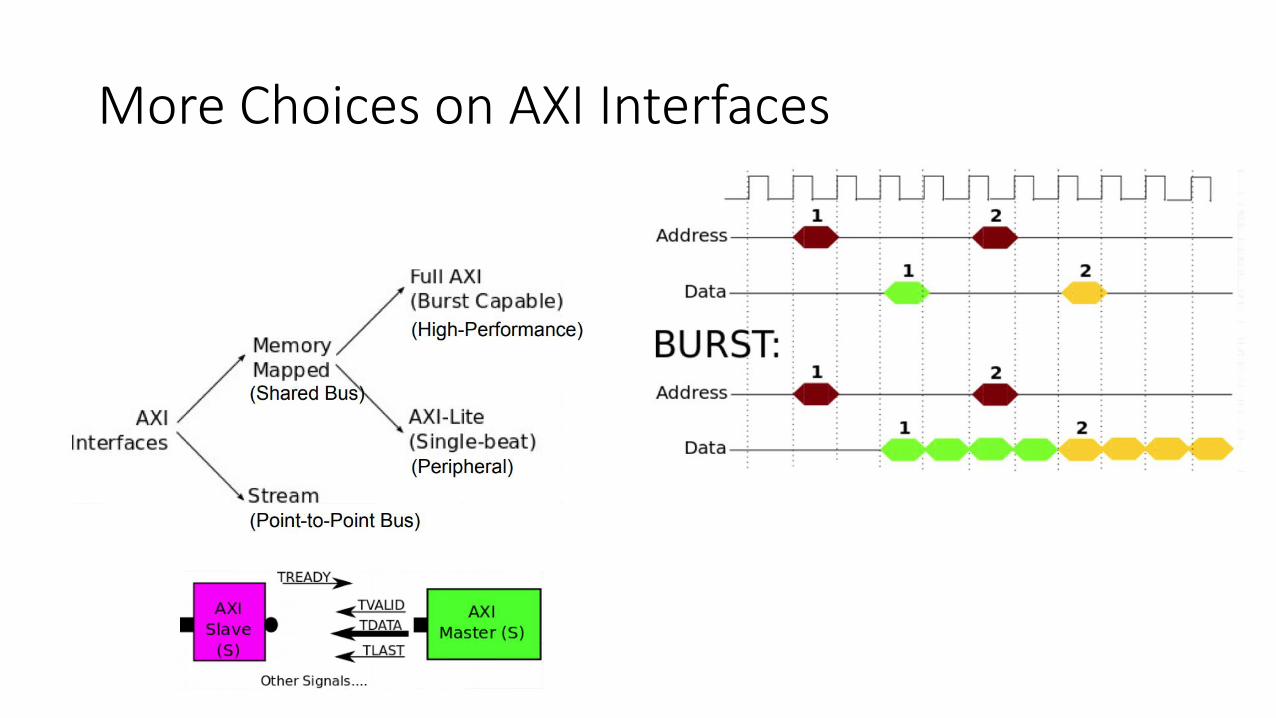
More Choices on AXI Interfaces
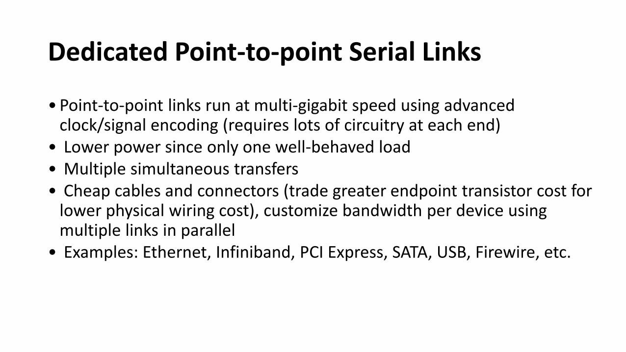
Dedicated Point-to-point Serial Links
• Point-to-point links run at multi-gigabit speed using advanced clock/signal encoding (requires lots of circuitry at each end)
• Lower power since only one well-behaved load• Multiple simultaneous transfers• Cheap cables and connectors (trade greater endpoint transistor cost for
lower physical wiring cost), customize bandwidth per device using multiple links in parallel
• Examples: Ethernet, Infiniband, PCI Express, SATA, USB, Firewire, etc.

AXI4 Read
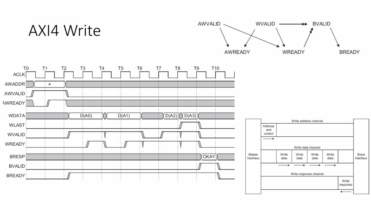
AXI4 Write

Direct Memory Access (DMA)
• DMA engines offload CPU by autonomously transferring data between I/O device and main memory. Interrupt/poll for done
• Often, many separate DMA engines in modern systems:• Centralized in I/O bridge (usually
supporting multiple concurrent channels to different devices), works on slave-only I/O busses
CPU
Caches
DRAM
I/O Bus Bridge
Memory Bus
I/O Bus
I/O Device
#1
I/O Device
#2
I/O Device
#3
DMA
DMA

Operation of a DMA Transfer
• DMA engine contains registers written by CPU: • Memory address to place data , # of bytes, I/O device #, direction of transfer
unit of transfer, amount to transfer per burst

DMA: Some new problems - I
• Where in the memory hierarchy do we plug in the DMA engine?
• Answer 1: Between L1 and CPU:
Pro: Free coherency
Con: Trash the CPU’s working set with transferred data
• Answer 2: Between Last-level cache and main memory
Pro: Don’t mess with caches
Con: Need to explicitly manage coherency

DMA: Some new problems - II
• How do we arbitrate between CPU and DMA Engine/Device access to memory? Three options:
• Burst Mode : Start transfer of data block, CPU cannot access memory in the meantime
• Cycle Stealing Mode : DMA engine transfers a byte, releases control, then repeats - interleaves processor/ DMA engine accesses
• Transparent Mode: DMA transfer only occurs when CPU is not using the system bus

More Complex Bus Structures
• Match speed of I/O connection to device demands• Special direct connection for
graphics
• Fast I/O bus for disk drives, ethernet
• Slow I/O bus for keyboard, mouse, touchscreen
• Reduces load on fast I/O bus + less bus logic needed on device
CPU
Caches
DRAM
I/O Bus BridgeMemory
Bus
Fast I/O Bus
I/O Device
#1
I/O Device
#3
Slow I/O Bus Bridge
DMA
I/O Device
#2
Slow I/O BusDMA
DMA
I/O Device
#4
Graphics
DMA
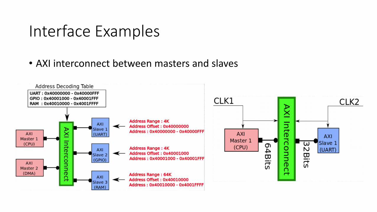
Interface Examples
• AXI interconnect between masters and slaves

Multi-master: Arbitration needed !
• There are three different arbitration schemes that use the centralized bus arbitration approach. There schemes are:
• a. Daisy chaining
• b. Polling method
• c. Independent request

Accelerators
• Use additional computational unit dedicated to some functions? • Hardwired logic.
• Extra CPU.
• Hardware/software co-design: joint design of hardware and software architectures
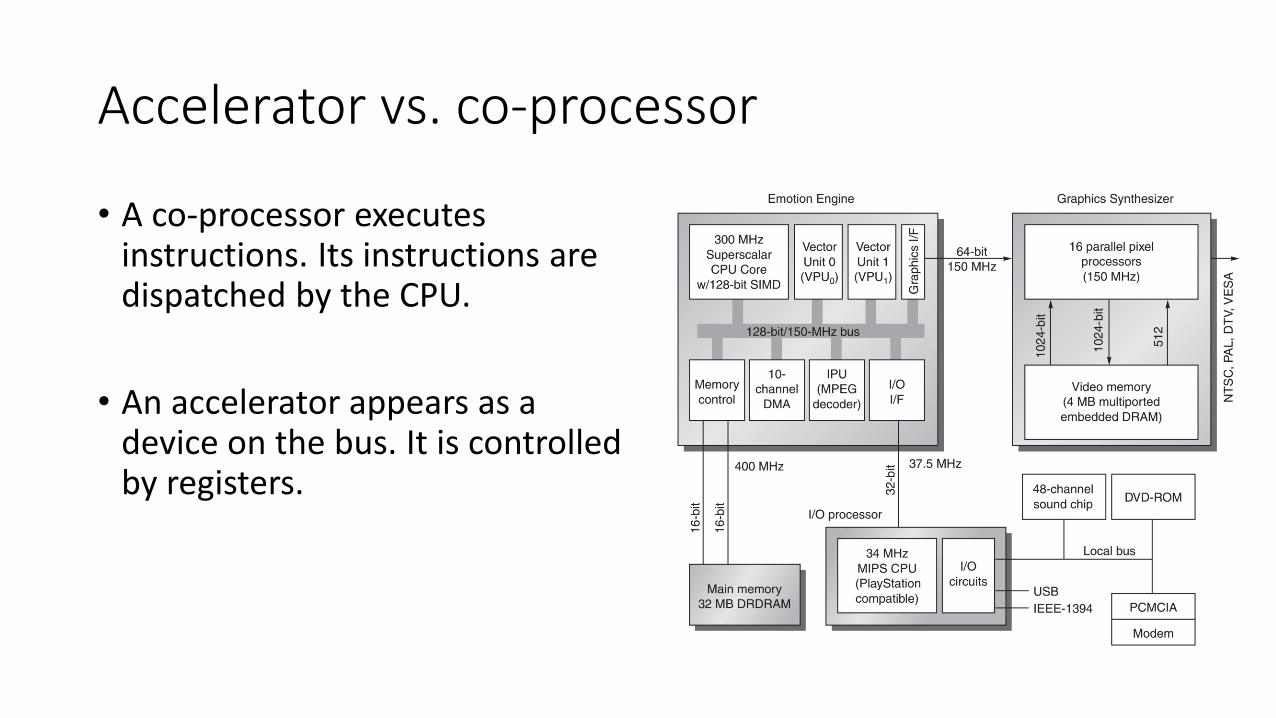
Accelerator vs. co-processor
• A co-processor executes instructions. Its instructions are dispatched by the CPU.
• An accelerator appears as a device on the bus. It is controlled by registers.

Why Accelerator ? In General
• Better cost/performance• Energy efficiency
• Real-time application
• Support Data streaming (audio, video, network traffic, real-time monitoring, etc.)
• Specific “complex” operations: FFT, DCT, EXP, LOG, …
• Specific “complex” algorithms: Neuronal networks, …

Why Accelerator ? Now it’s mandatory
• Moore’s Law
• More pipelined stages?
• Multi Core?
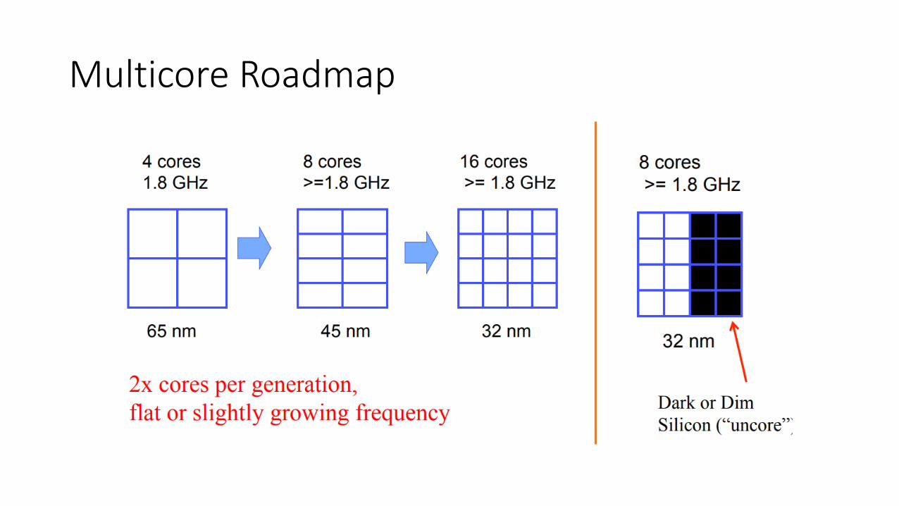
Multicore Roadmap

General Purpose Processor hit the utilization wall• Utilization Wall: With each successive
process generation, the percentage of a chip that can actively switch drops exponentially due to power constraints.
• Experimental results • Replicated a small datapath
• More "dark silicon" than active
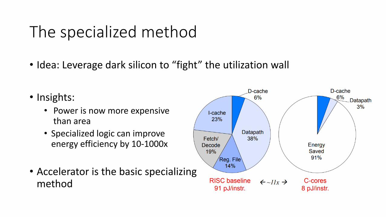
The specialized method
• Idea: Leverage dark silicon to “fight” the utilization wall
• Insights: • Power is now more expensive
than area
• Specialized logic can improve energy efficiency by 10-1000x
• Accelerator is the basic specializingmethod
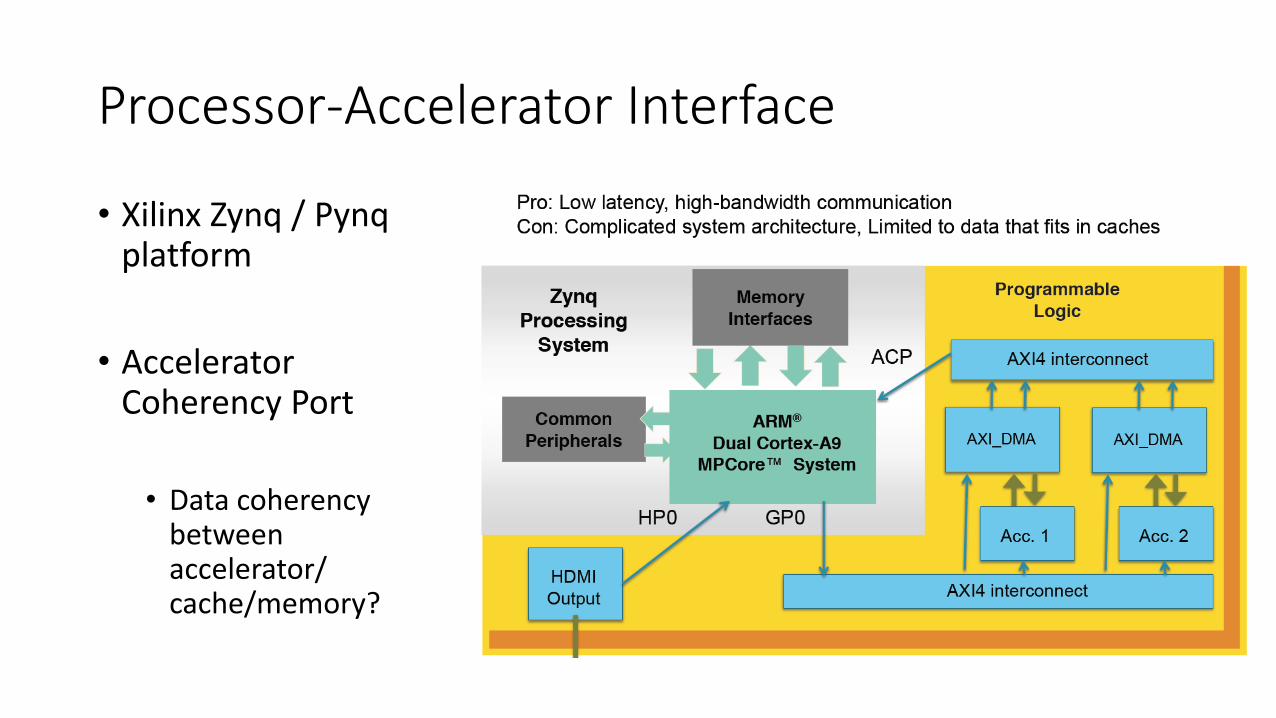
Processor-Accelerator Interface
• Xilinx Zynq / Pynqplatform
• Accelerator Coherency Port
• Data coherency between accelerator/ cache/memory?

Interface : Streaming FIFO
• Three user-side AXI Stream interfaces: TX data, RX data, TX control

Interface : AXI DMA Controllwer
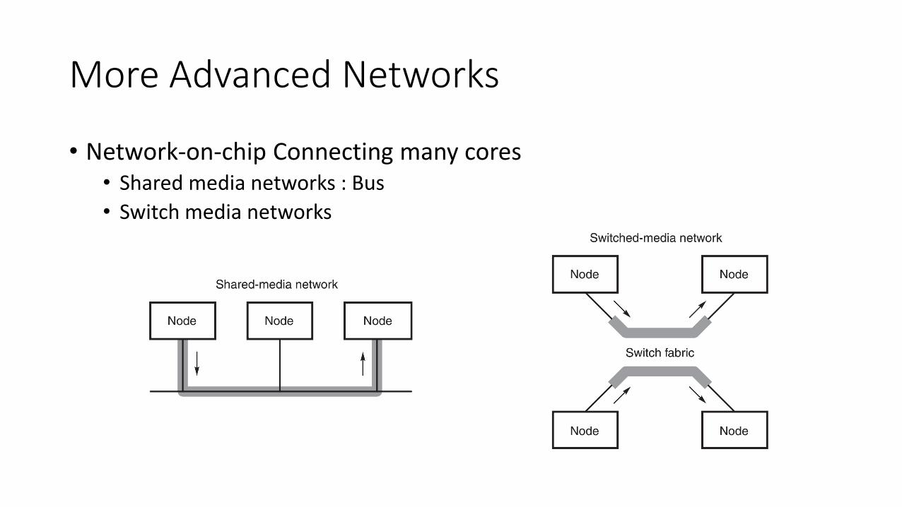
More Advanced Networks
• Network-on-chip Connecting many cores • Shared media networks : Bus
• Switch media networks

Crossbar On-Chip
• Busses evolved in era where wires were expensive and had to be shared
• Crossbar exploits density of on-chip wiring, allows multiple simultaneous transactions
How many switches for N nodes cross bar?

Distributed Ring/Mesh networks
There are cases where it is convenient to more tightly integrate the end node devices with the network resources used to enable them to communicate.
Distribute the network switches among the end nodes
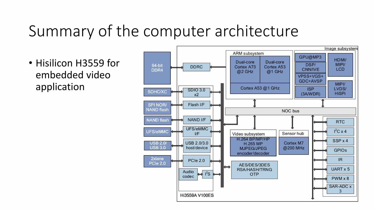
Summary of the computer architecture
• Hisilicon H3559 forembedded videoapplication