burn-in & test socket workshop & test socket workshop session 5 ... 860 ph 310 ph 78 ff 23...
TRANSCRIPT

March 3-6 , 2002Hilton Phoenix East/Mesa Hotel
Mesa, Arizona
Sponsored By The IEEE Computer SocietyTest Technology Technical Council
Burn-in & TestSocket Workshop
IEEE IEEE
COMPUTERSOCIETY

COPYRIGHT NOTICE• The papers in this publication comprise the proceedings of the 2002BiTS Workshop. They reflect the authors’ opinions and are reproduced aspresented , without change. Their inclusion in this publication does notconstitute an endorsement by the BiTS Workshop, the sponsors, or theInstitute of Electrical and Electronic Engineers, Inc.· There is NO copyright protection claimed by this publication. However,each presentation is the work of the authors and their respectivecompanies: as such, proper acknowledgement should be made to theappropriate source. Any questions regarding the use of any materialspresented should be directed to the author/s or their companies.

Burn-in & Test SocketWorkshop
Session 5Tuesday 3/05/02 1:00PM
Modeling, Analysis and Characterization
“Electrical Modeling And Contactor Performance In A RF System”Jim Adley - Johnstech International CorporationEric Leung - Johnstech International CorporationJeff Sherry - Johnstech International Corporation
“Leaded 2mm Contactors: Measuring And Modeling To 10 GHz”Tom Strouth - GigaTest Labs Orlando Bell - GigaTest LabsGary Otonari - GigaTest Labs Eric Bogatin - GigaTest Labs
Jeff Sherry - Johnstech International Corporation
“Force Measurement On Sockets And Contactors”Richard Block - Advanced Micro DevicesRafiq Hussain - Advanced Micro Devices
Technical Program

1
Electrical Modeling andContactor Performance in a RF
Test System0.5 mm Pitch BGA
Jim Adley, R&D ManagerEric Leung, R&D EngineerJeff Sherry, R&D Engineer
Johnstech International

2
Discussion Topics
Modeled Data
Measured Data
Comparative Data
Equivalent Circuit Model
Conclusion
3
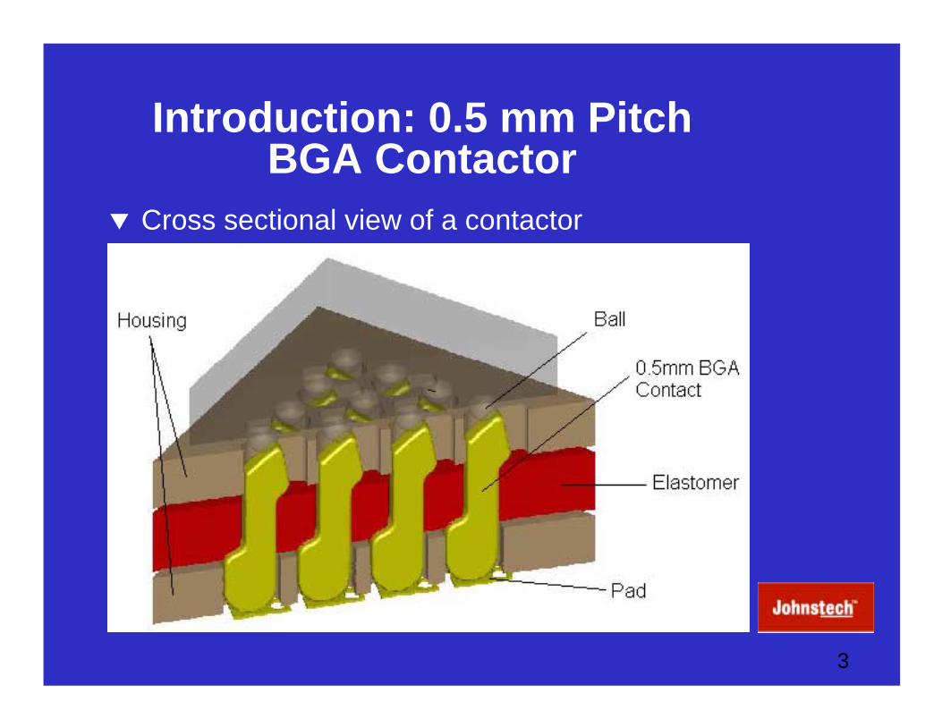
Introduction: 0.5 mm PitchBGA Contactor
Cross sectional view of a contactor
4
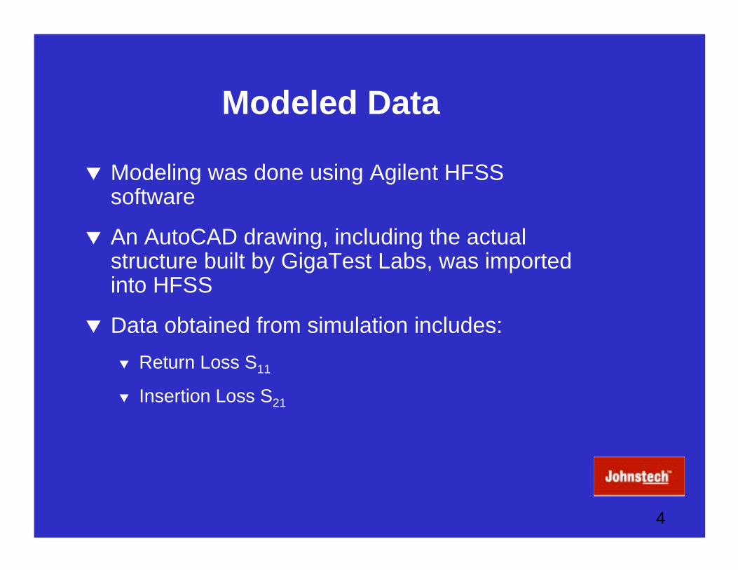
Modeled Data
Modeling was done using Agilent HFSSsoftware
An AutoCAD drawing, including the actualstructure built by GigaTest Labs, was importedinto HFSS
Data obtained from simulation includes: Return Loss S11
Insertion Loss S21
5
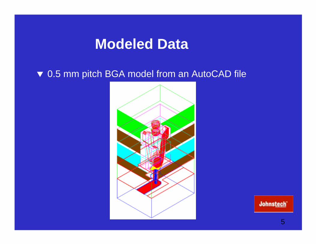
Modeled Data
0.5 mm pitch BGA model from an AutoCAD file

6
Modeled Data - S11 This is data from the HFSS model of return
loss by the actual 0.5 mm BGA structuretested by GigaTest Labs
-50
-45
-40
-35
-30
-25
-20
-15
-10
-5
0
1 2 3 4 5 6 7 8 9 10
Frequency (GHz)
Retu
rn L
oss
(dB
)
HFSS 0.5mm Pitch Adjacent BGA Contact Model
Optimum Load Board Layout of HFSS 0.5mm Pitch AdjacentBGA Contact Model
7
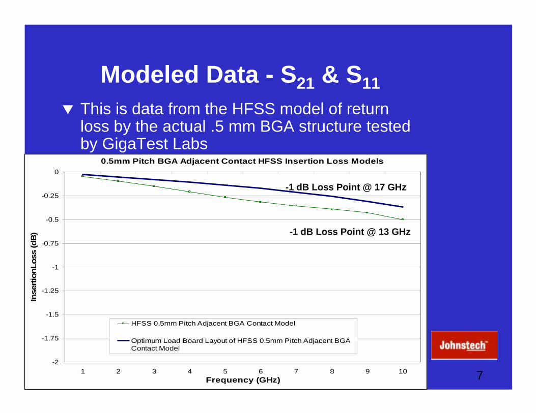
Modeled Data - S21 & S11 This is data from the HFSS model of return
loss by the actual .5 mm BGA structure testedby GigaTest Labs
0.5mm Pitch BGA Adjacent Contact HFSS Insertion Loss Models
-2
-1.75
-1.5
-1.25
-1
-0.75
-0.5
-0.25
0
1 2 3 4 5 6 7 8 9 10Frequency (GHz)
Inse
rtion
Loss
(dB
)
HFSS 0.5mm Pitch Adjacent BGA Contact Model
Optimum Load Board Layout of HFSS 0.5mm Pitch Adjacent BGAContact Model
-1 dB Loss Point @ 17 GHz
-1 dB Loss Point @ 13 GHz

8
Modeled Data
HFSS Capabilities Contact design parameters
Load board design effects
Device pad interactions
Expected performance
Effects of tolerances
Interaction between components in system(device, contactor, handler, etc.)
Trends

9
Measured Data
GigaTest Labs tested a 0.5 mm pitch BallSeries contactor
GigaTest Labs used a surrogate device -Short, Open, Load, Thru (SOLT) to conducttesting
Data was measured by GigaTest Labsthrough probing from the back side of anon-optimized load board

10
Measured Data
Surrogate Circuit

11
Measured Data GigaTest Labs used a micro probe station for
measuring two adjacent contacts S-parameters

12
Measured Data
The 0.5 mm pitch BGA housing and BGAsurrogate package

13
Comparative DataHFSS Model vs. Measured Test Data for 0.5mm BGA Adjacent Contacts
-50
-45
-40
-35
-30
-25
-20
-15
-10
-5
0
0 1 2 3 4 5 6 7 8 9 10Frequency (GHz)
Ret
urn
Loss
(dB
)
HFSS 0.5mm Pitch Adjacent BGA Contact Model
Measured Test Data from GigaTest Labs for 0.5mm Adjacent BGAContact (Non-Optimum pads)
-20 dB Measured Loss Point @ 2.95 GHz

14
Comparative Data0.5mm Pitch BGA Adjacent Contact Modeled vs. Measured Test Data
-2
-1.75
-1.5
-1.25
-1
-0.75
-0.5
-0.25
0
0 1 2 3 4 5 6 7 8 9 10Frequency (GHz)
Inse
rtion
Los
s (d
B)
HFSS 0.5mm Pitch Adjacent BGA Contact Model
Measured Test Data from GigaTest Labs for 0.5mm Adjacent BGA Contact (Non-Optimum pads)
-1 dB Measured Loss Point @ 10.3 GHz
15
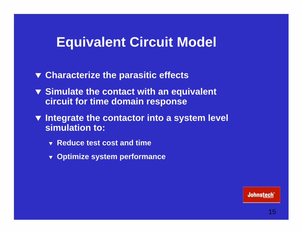
Equivalent Circuit Model
Characterize the parasitic effects
Simulate the contact with an equivalentcircuit for time domain response
Integrate the contactor into a system levelsimulation to:
Reduce test cost and time
Optimize system performance

16
Equivalent Circuit Model
Measure the S-parameters for short-, open- andthru- fixtures from two adjacent contacts
Use measured data and Agilent AdvancedDesign System (ADS) for model extraction andverification
Compare measured and ADS simulatedinsertion and return loss

17
Equivalent Circuit Model
This figure shows the Equivalent Circuit Modelfor two adjacent 0.5 mm BGA contacts

18
Equivalent Circuit Model0.5mm Pitch BGA Adjacent Contact ADS Equivalent
Circuit Model vs. Measured Test Data
-60
-50
-40
-30
-20
-10
0
0 1 2 3 4 5 6 7 8 9 10Frequency (GHz)
Ret
urn
Loss
(dB
)
ADS Return Loss Model for 0.5mm Adjacent BGA Contact From EquivalentCircuit Measured Test Data from GigaTest Labs for 0.5mm Adjacent BGAContact (Non-Optimum pads)
-20 dB Measured Loss Point @ 2.95 GHz
19
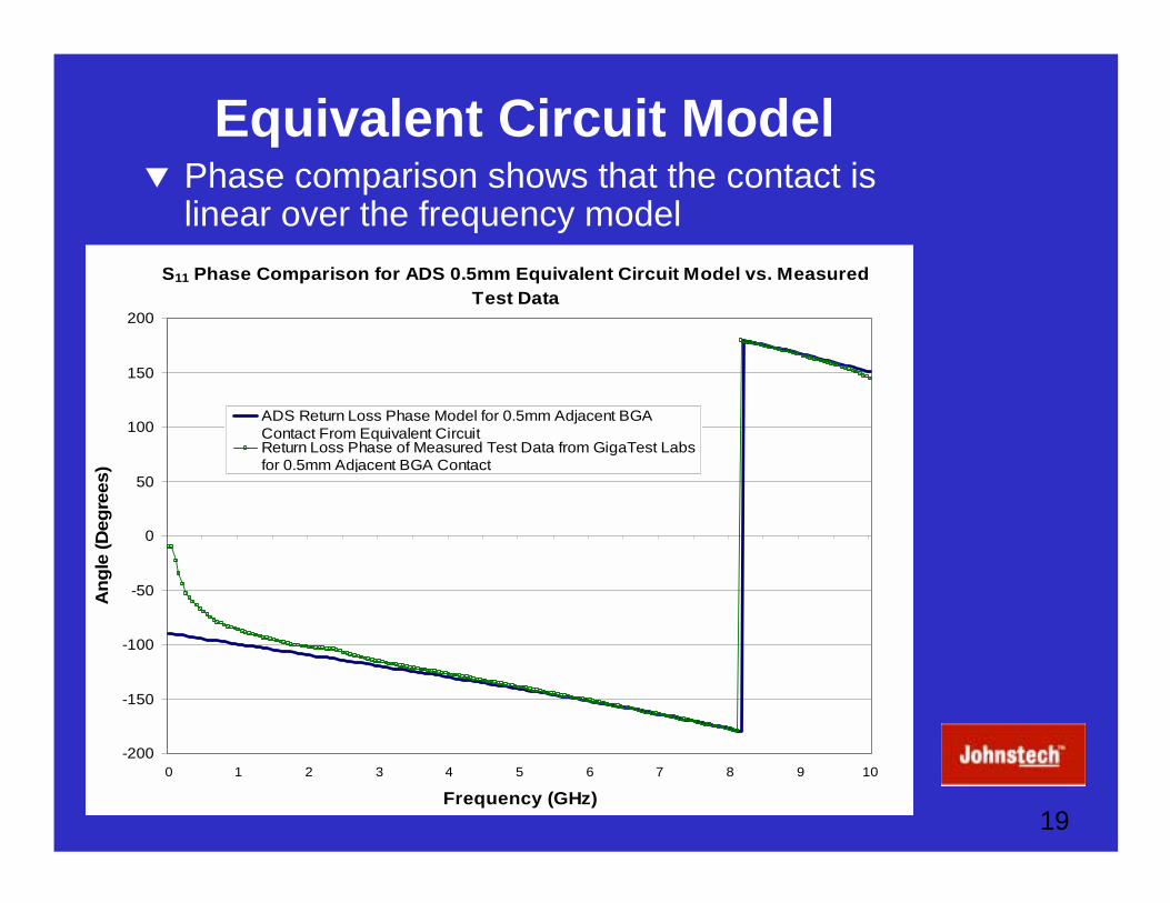
Equivalent Circuit Model Phase comparison shows that the contact is
linear over the frequency modelS11 Phase Comparison for ADS 0.5mm Equivalent Circuit Model vs. Measured
Test Data
-200
-150
-100
-50
0
50
100
150
200
0 1 2 3 4 5 6 7 8 9 10
Frequency (GHz)
Ang
le (D
egre
es)
ADS Return Loss Phase Model for 0.5mm Adjacent BGAContact From Equivalent Circuit Return Loss Phase of Measured Test Data from GigaTest Labsfor 0.5mm Adjacent BGA Contact

20
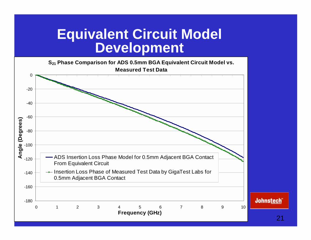
Equivalent Circuit ModelDevelopment
0.5mm BGA Adjacent Contact Insertion Loss (S11) ADS Equivalent Circuit Model vs. Measured Test Data
-2
-1.5
-1
-0.5
0
0 1 2 3 4 5 6 7 8 9 10Frequency (GHz)
Inse
rtion
Los
s (d
B)
ADS Insertion Loss Model for 0.5mm Adjacent BGA Contact FromEquivalent Circuit Measured Test Data from GigaTest Labs for 0.5mm AdjacentBGA Contact (Non-Optimum pads)
-1 dB Measured Loss Point @ 10.3 GHz
21
Equivalent Circuit ModelDevelopment
S21 Phase Comparison for ADS 0.5mm BGA Equivalent Circuit Model vs. Measured Test Data
-180
-160
-140
-120
-100
-80
-60
-40
-20
0
0 1 2 3 4 5 6 7 8 9 10Frequency (GHz)
Ang
le (D
egre
es)
ADS Insertion Loss Phase Model for 0.5mm Adjacent BGA ContactFrom Equivalent Circuit Insertion Loss Phase of Measured Test Data by GigaTest Labs for0.5mm Adjacent BGA Contact
22
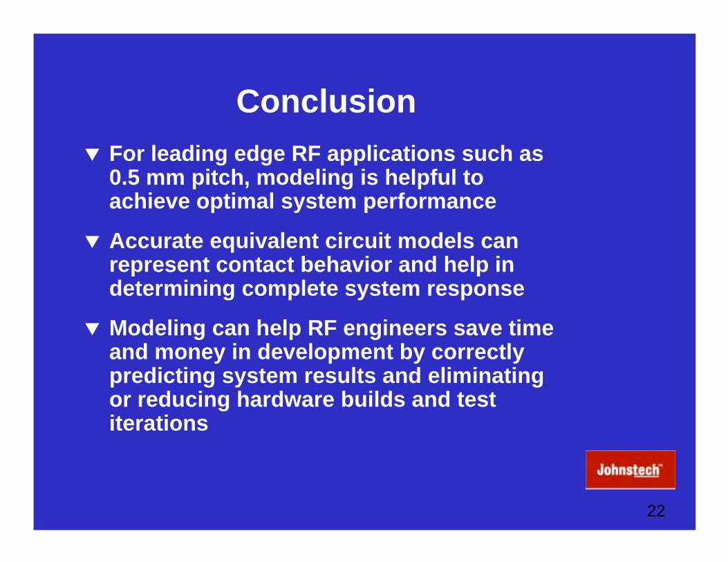
Conclusion For leading edge RF applications such as
0.5 mm pitch, modeling is helpful toachieve optimal system performance
Accurate equivalent circuit models canrepresent contact behavior and help indetermining complete system response
Modeling can help RF engineers save timeand money in development by correctlypredicting system results and eliminatingor reducing hardware builds and testiterations

Leaded 2 mm Contactors:Measuring and Modeling to 10 GHz
Tom Strouth, Orlando Bell, Gary Otonari, Eric BogatinGigaTest Labs, www.GigaTest.com
andJeff Sherry
Johnstech, www.Johnstech.com

BiTS 2002
Slide - 2
Outline
• Contactors• Fixturing• Measurement set up• Modeling process• Results• Using the model for simulation

BiTS 2002
Slide - 3
32 lead MLP2 Contactor
BiTS 2002
Slide - 4
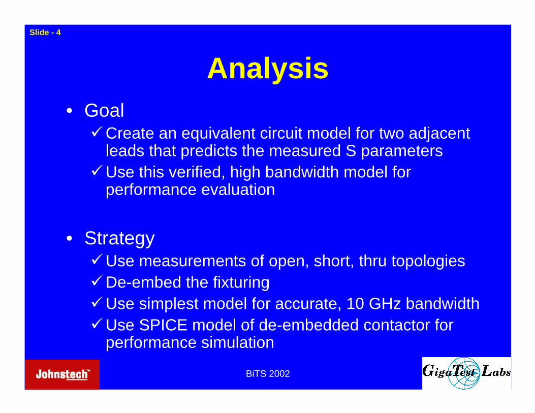
Analysis• Goal
Create an equivalent circuit model for two adjacentleads that predicts the measured S parameters
Use this verified, high bandwidth model forperformance evaluation
• StrategyUse measurements of open, short, thru topologiesDe-embed the fixturingUse simplest model for accurate, 10 GHz bandwidthUse SPICE model of de-embedded contactor for
performance simulation
BiTS 2002
Slide - 5
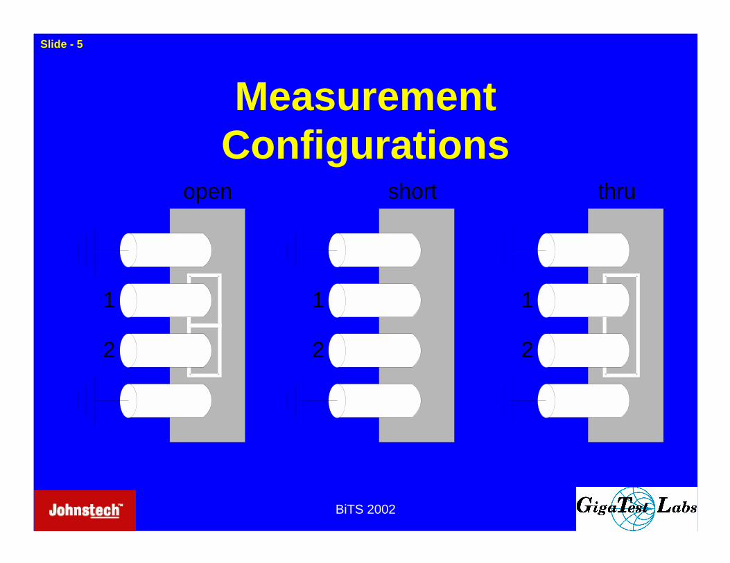
MeasurementConfigurations
1
2
1
2
1
2
open short thru

BiTS 2002
Slide - 6
Surrogate Package:
open
shortthru
Enables configuring open, short, thruconnections for edge and corner leads

BiTS 2002
Slide - 7
Instrument Set Up

BiTS 2002
Slide - 8
Probing From the Back Side
Probing using microprobes and aProbing using microprobes and aGigaTest Probe StationGigaTest Probe Station

BiTS 2002
Slide - 9
Modeling the System withAgilent ADS
VNAVNA FixtureFixtureboardboard
Pads andPads andcontactorcontactor
SurrogateSurrogatepackagepackage
short
open
short
Lcbg

BiTS 2002
Slide - 10
Methodology• Measure S parameters of calibration vias in bare fixture
board• Extract model for just the fixture• Select two adjacent corner leads (longest leads)• Measure open, short, thru for the pair of leads• Extract model of contactor pins and surrogate package• Use de-embedded contactor circuit model to simulate
performance
BiTS 2002
Slide - 11
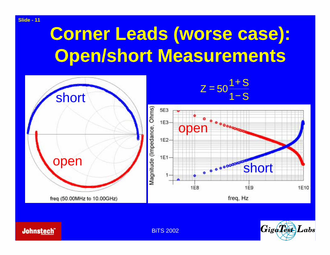
Corner Leads (worse case):Open/short Measurements
S1S150Z
−+=
open
short
open
short

BiTS 2002
Slide - 12
Optimized Model: OpenImpedance of one trace Coupling between traces
Solid Line is Simulated

BiTS 2002
Slide - 13
Optimized Model: Open
Reflection Transmission
Open provides mutual capacitance info
Triangles (purple): Measured
BiTS 2002
Slide - 14
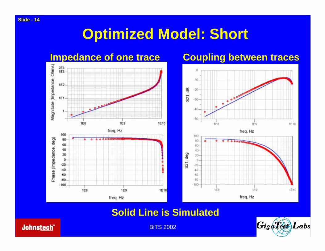
Optimized Model: ShortImpedance of one trace Coupling between traces
Solid Line is Simulated

BiTS 2002
Slide - 15
Optimized Model: ShortReflection Transmission (coupling)
Short provides mutual inductance info
Triangles (purple): Measured
BiTS 2002
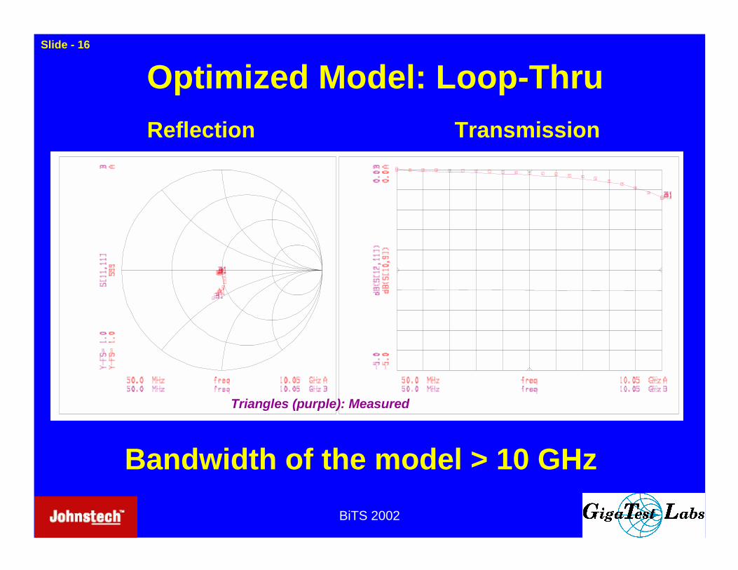
Slide - 16
Optimized Model: Loop-ThruReflection Transmission
Bandwidth of the model > 10 GHz
Triangles (purple): Measured

BiTS 2002
Slide - 17 Summary of ExtractedParameters
VNAVNA FixtureFixture ContactorContactor
23 pH23 pH
140 140 fFfF
89 89 fFfF 860 pH860 pH
310 pH310 pH78 78 fFfF
23 pH23 pH
140 140 fFfF 89 89 fFfF860 pH860 pH
SurrogateSurrogateNote: load board was not optimized for performance
151 151 fFfF 33 pH33 pH
25 25 fFfF133 133 fFfF
151 151 fFfF33 pH33 pH
33 pH33 pH

BiTS 2002
Slide - 18
De-Embedded Insertion andReturn Loss of Contactor
Meets specification:< -20 dB, below 10 GHz
Meets specification:> -1 dB, below 10 GHz
Return loss Insertion loss
Note: load board is not optimized for performance,Note: load board is not optimized for performance,standard contactor - standard contactor - notnot enhanced contactor enhanced contactor

BiTS 2002
Slide - 19
Transient Simulation UsingDe-embedded Contactor Model
Specs:
De-embedded contactormodel
20 psec rise time
50 Ω source, termination
Differential drive

BiTS 2002
Slide - 20
Transient Simulationwith 20 psec Rise Time
• 20 psec input rise time
• 28 psec output rise time
• 20 psec intrinsicinterconnect rise time(> 15 GHz bandwidth)
• 21 psec time delay
Note: load board is not optimized for performance,Note: load board is not optimized for performance,standard contactor - standard contactor - notnot enhanced contactor enhanced contactor
BiTS 2002
Slide - 21
Conclusions• A contactor model can be de-embedded
from S-parameter measurements
• A simple model matches measured data upto at least 10 GHz. (model could have morebandwidth)
• A model extracted from frequency domainmeasurements can be used in a transientsimulation.
Force Measurement onSockets and Contactors
2002 Burn-in and Test Socket WorkshopMarch 3 - 6, 2002
Presenter: Richard BlockRafiq Hussain
Jan 10, 2002 Force Measurement on Sockets &Contactors
2
Agenda
• Force Issues in Test and Burn-In Env.• Force Measurement Unit• Experimentation & Test Data• Conclusions• Looking Forward

Jan 10, 2002 Force Measurement on Sockets &Contactors
3
Force Issues in Test andBurn-In Env.
• Bent Pins / Deformed Balls• Overdriving of Pogos• Crack/Chipped Die or Pkg• Pkg warping• Force Distribution

Jan 10, 2002 Force Measurement on Sockets &Contactors
4
Force Measurement Unit
• Simple Design– 1 transducer– 2 spacers– 1 digital display (giving real-time force
readouts to 0.1 lb accuracy)• Location
– Replaced support under PCB and Socket

Jan 10, 2002 Force Measurement on Sockets &Contactors
5
FMU consists of 3 pcs2 spacers1 transducer
PCB
DUT
Thermal Head

Jan 10, 2002 Force Measurement on Sockets &Contactors
6
Board Deflection
• Motherboard deflection was necessary fortransducer to take measurements– Motherboard was 62 mils thick– Transducer max deflection was 3 mils for 250lbs– Deflection did not create any noticeable error in
force readout• 2 lb, 5 lb, and 10 lb weights were used for confirmation
Jan 10, 2002 Force Measurement on Sockets &Contactors
7
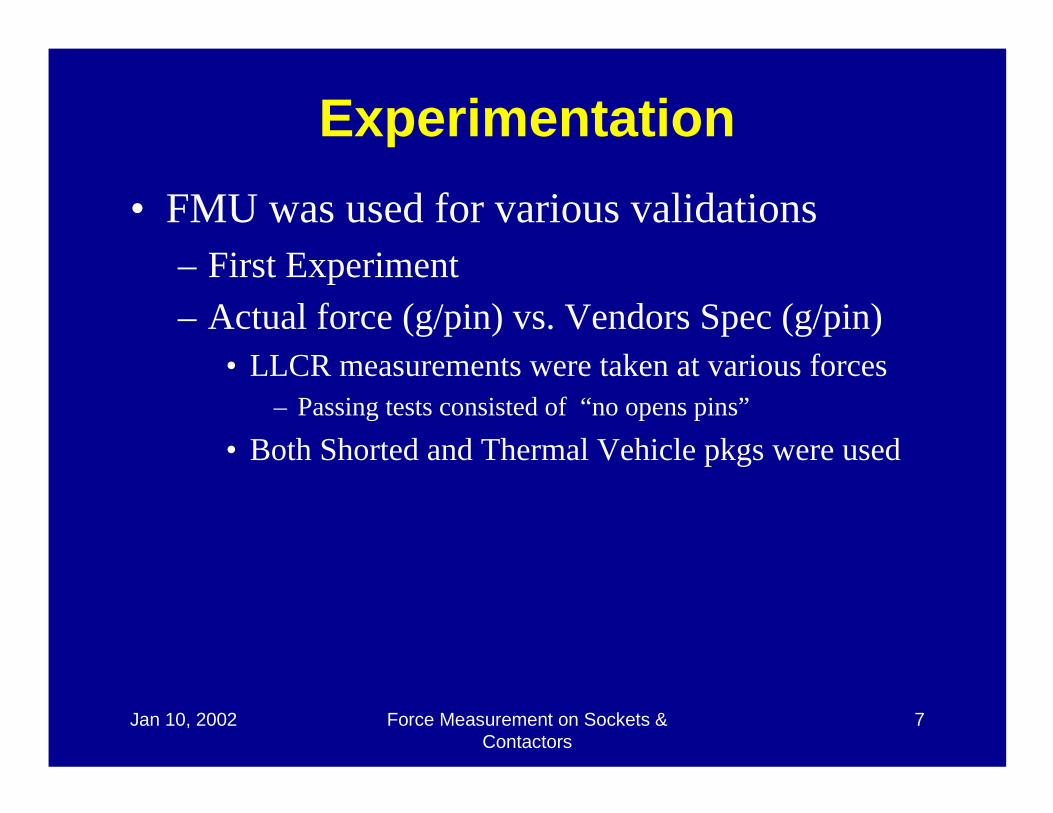
Experimentation• FMU was used for various validations
– First Experiment– Actual force (g/pin) vs. Vendors Spec (g/pin)
• LLCR measurements were taken at various forces– Passing tests consisted of “no opens pins”
• Both Shorted and Thermal Vehicle pkgs were used

Jan 10, 2002 Force Measurement on Sockets &Contactors
8
Actual Force vs. Vendor Spec
15
12
28
11
15
18
25
18
12
28
1716
25
16
0
5
10
15
20
25
30
A B (1) B (2) C D E F
Vendor
Forc
e (g
ram
s/pi
n)
Vendor Spec.Actual

Jan 10, 2002 Force Measurement on Sockets &Contactors
9
• FMU was used for various validations– Second Experiment– Insertion study to find optimal force vs. Pogo life
Experimentation cont.
•Second run:–100,000 insertions at different force–LLCR measurements were compared to first run
•First run:–100,000 insertions were made at ideal force firstexperiment–LLCR measurements were taken periodically to see ifresistance values increased

Jan 10, 2002 Force Measurement on Sockets &Contactors
10
Insertion Life vs. ForceVendor Insertions ave ohms Vendor Insertions ave ohms
A Low 22.02 D Low 23.3718 g/p 25 k 22.04 16 g/p 25 k 22.75
50 k 22.10 50 k 22.7075 k 22.09 75 k 22.57
B (1) Low 23.11 E Low 22.2412 g/p 25 k 23.27 25 g/p 25k 22.10
50 k 22.93 50k 22.3475 k 22.68 75k 22.30
96 k 22.14
C Low 22.82 F Low 22.2517 g/p 40 k 22.04 16 g/p 25 k 22.47
80 k 22.16 50 k 22.3075 k 22.38

Jan 10, 2002 Force Measurement on Sockets &Contactors
11
Insertion Life vs. Force cont.Vendor Insertions ave ohms
B (1)Low 23.11
15 g/p 30 k 23.4150 k 23.2170 k 23.21
DLow 22.57
19 g/p 25 k 22.7340 k 22.40
ELow 22.24
28 g/p 25k 26.6775k 26.35
• Insertions were done ata greater force then firstseries of insertions.– ~3 to 4 g/p depending on
initial required force• Vendor D had pin
failures at this higherforce
Jan 10, 2002 Force Measurement on Sockets &Contactors
12
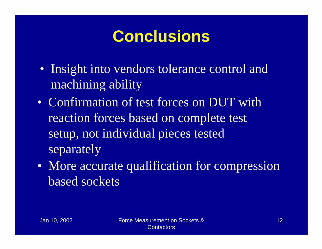
Conclusions
• Insight into vendors tolerance control andmachining ability
• Confirmation of test forces on DUT withreaction forces based on complete testsetup, not individual pieces testedseparately
• More accurate qualification for compressionbased sockets

Jan 10, 2002 Force Measurement on Sockets &Contactors
13
Looking Forward
• Die size Transducers
• Force variation across die/pkg

Jan 10, 2002 Force Measurement on Sockets &Contactors
14
Plunger
TransducerContactor Alignment Plate
Transducer for HandlersExample
Jan 10, 2002 Force Measurement on Sockets &Contactors
15
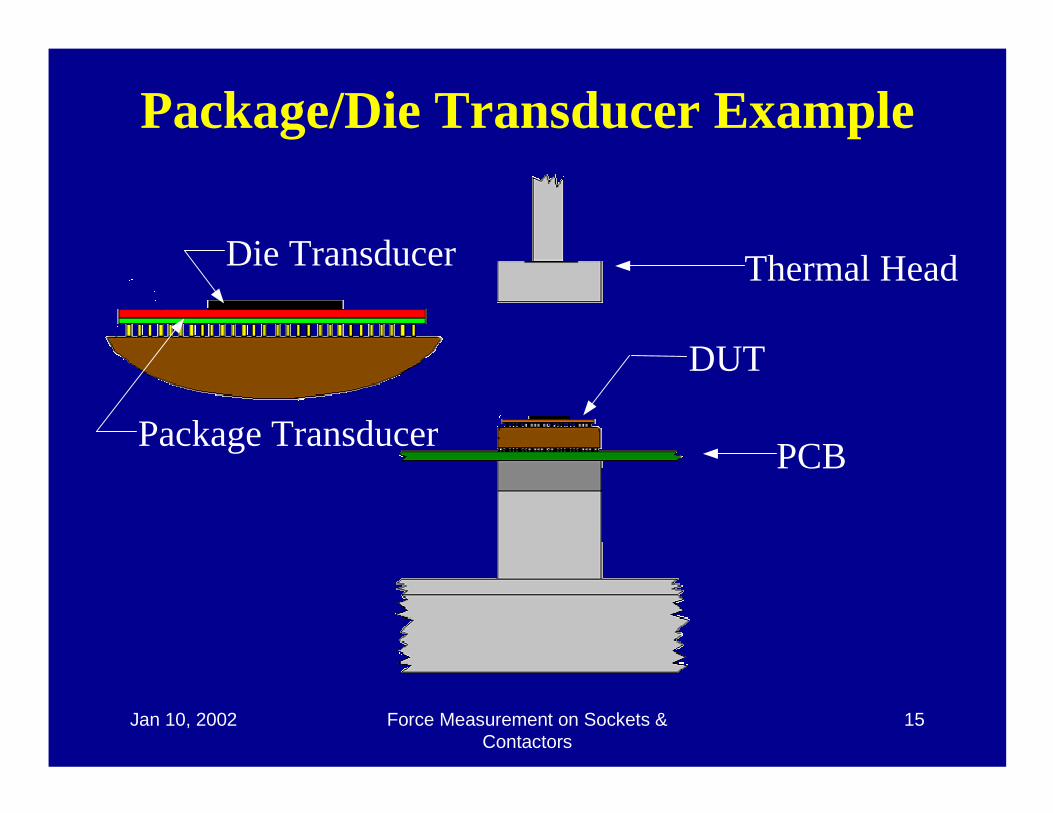
Package/Die Transducer Example
PCB
DUT
Thermal Head
Package Transducer
Die Transducer
Jan 10, 2002 Force Measurement on Sockets &Contactors
16
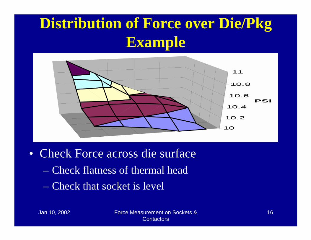
Distribution of Force over Die/PkgExample
10
10.2
10.4
10.6
10.8
11
PSI
• Check Force across die surface– Check flatness of thermal head– Check that socket is level