bridging the gap : co-optimization of physical design...
TRANSCRIPT

© 2012 IBM Corporation
IBM Research and STG Group
Bridging the Gap : Co-Optimization of Physical Design and DFM
Gi-Joon Nam, Shayak Banerjee, Kanak Agarwal, Sani Nassif
June 02, 2013

IBM Research & STG Group
© 2012 IBM Corporation 2
Outline
Issues with 22nm design flow
Designer’s wish list
Fundamental techniques in timing closure
Lithography-Aware Physical Synthesis (Top-down)
Co-Optimization of PD and DFM – Wire delay variability impact on PD optimization

IBM Research & STG Group
© 2012 IBM Corporation 3
Typical Design Flow: How to Make a Chip
Source: A. Kahng, J. Lienig, I. Markov, J. Hu, VLSI Physical Design: From Graph Partitioning To Timing Closure, Springer, 2011
GDSII
Masks

IBM Research & STG Group
© 2012 IBM Corporation 4
Typical Design Flow: How to Make a Chip
Source: A. Kahng, J. Lienig, I. Markov, J. Hu, VLSI Physical Design: From Graph Partitioning To Timing Closure, Springer, 2011
Large Changes
Small Changes
Low Accuracy
High Accuracy

IBM Research & STG Group
© 2012 IBM Corporation 5
Chip (Circuit) Entities
How do we manufacture it efficiently and effectively ???

IBM Research & STG Group
© 2012 IBM Corporation 6
Transistor Manufacturing Process

IBM Research & STG Group
© 2012 IBM Corporation 7
Then Interconnect Manufacturing

IBM Research & STG Group
© 2012 IBM Corporation 9
Design Costs are Increasing per Process Node
Source: International Business Strategies, July 2010

IBM Research & STG Group
© 2012 IBM Corporation 10
Typical Design Flow: What’s missing…..
Source: A. Kahng, J. Lienig, I. Markov, J. Hu, VLSI Physical Design: From Graph Partitioning To Timing Closure, Springer, 2011

IBM Research & STG Group
© 2012 IBM Corporation 11
Typical Design Flow: What’s missing…..
Source: A. Kahng, J. Lienig, I. Markov, J. Hu, VLSI Physical Design: From Graph Partitioning To Timing Closure, Springer, 2011

IBM Research & STG Group
© 2012 IBM Corporation 12
Concerns with today’s design process (I.e. objective functions)
Timing
Power
Turn-around Time
Routability
Signal Integrity
Clocking
and more…..

IBM Research & STG Group
© 2012 IBM Corporation 13
Concerns with today’s design process (I.e. objective functions)
Timing
Power
Turn-around Time
Routability
Signal Integrity
Clocking
and more…..
Where is DFM Optimization???
Where is Lithography Optimization???
IBM Research & STG Group
© 2012 IBM Corporation 14
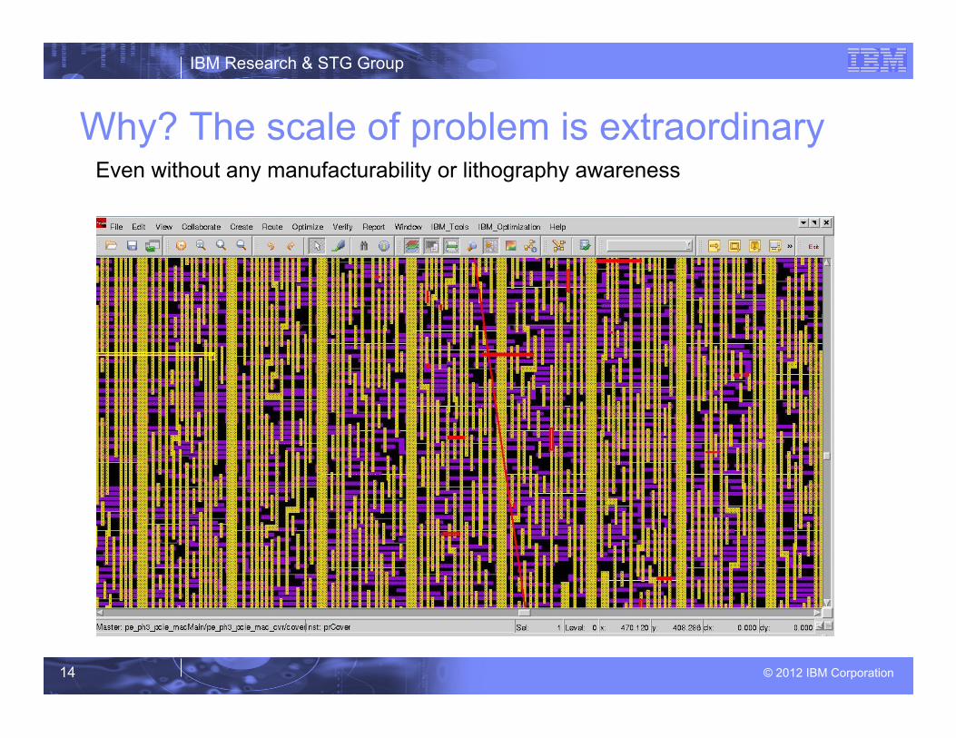
Why? The scale of problem is extraordinary Even without any manufacturability or lithography awareness
IBM Research & STG Group
© 2012 IBM Corporation 15
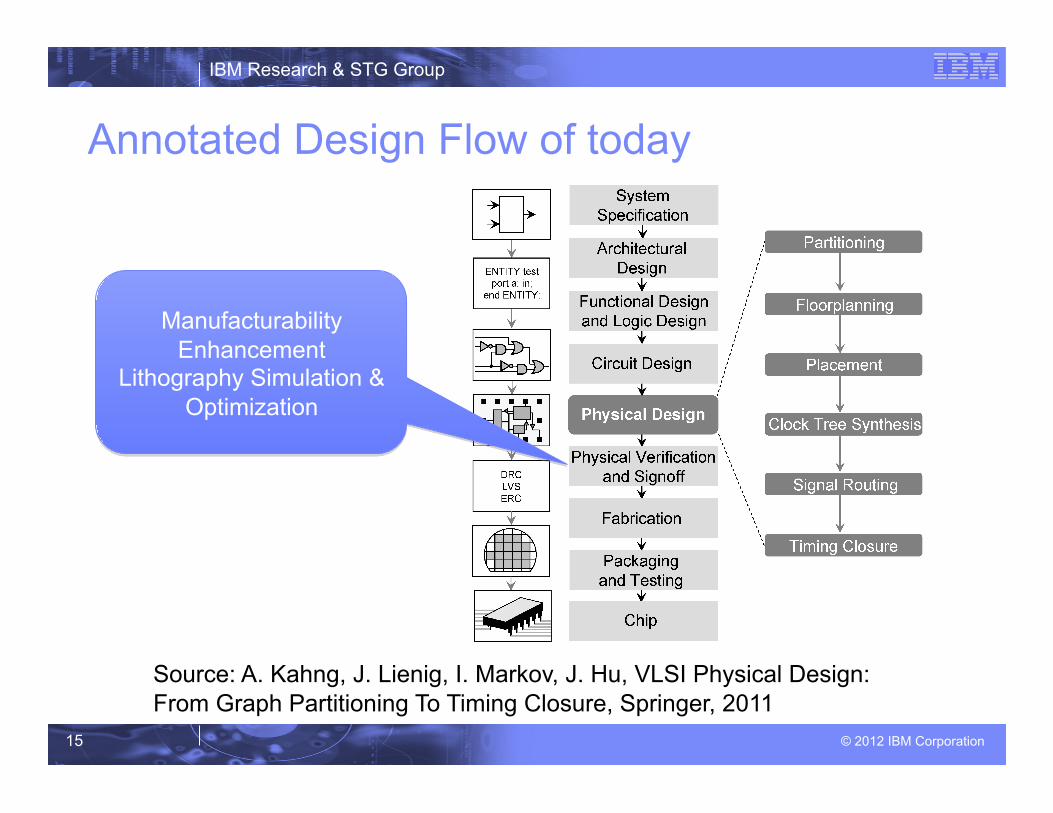
Annotated Design Flow of today
Source: A. Kahng, J. Lienig, I. Markov, J. Hu, VLSI Physical Design: From Graph Partitioning To Timing Closure, Springer, 2011
Manufacturability Enhancement
Lithography Simulation & Optimization

IBM Research & STG Group
© 2012 IBM Corporation 16
Outline
Issues with 22nm design flow
Designer’s wish list
Fundamental techniques in timing closure
Lithography-Aware Physical Synthesis (Top-down)
Co-Optimization of PD and DFM – Wire delay variability impact on PD optimization
IBM Research & STG Group
© 2012 IBM Corporation 17
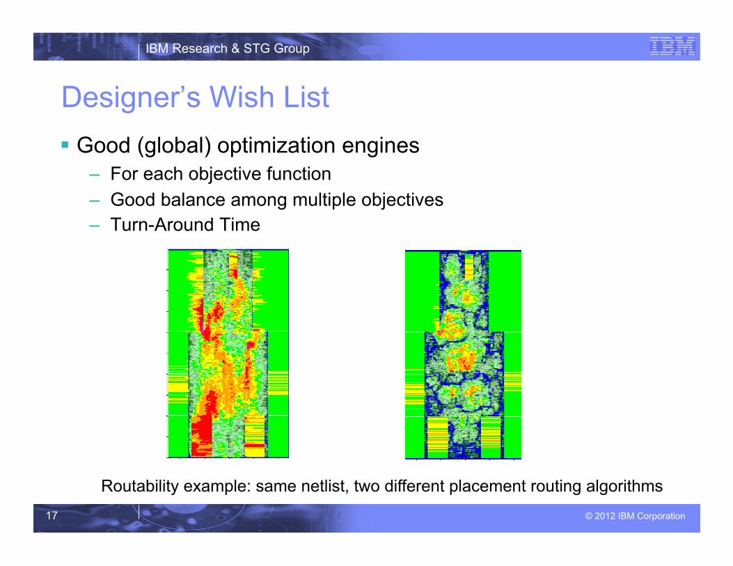
Designer’s Wish List Good (global) optimization engines
– For each objective function – Good balance among multiple objectives – Turn-Around Time
.245 mm 2
Routability example: same netlist, two different placement routing algorithms
IBM Research & STG Group
© 2012 IBM Corporation 18
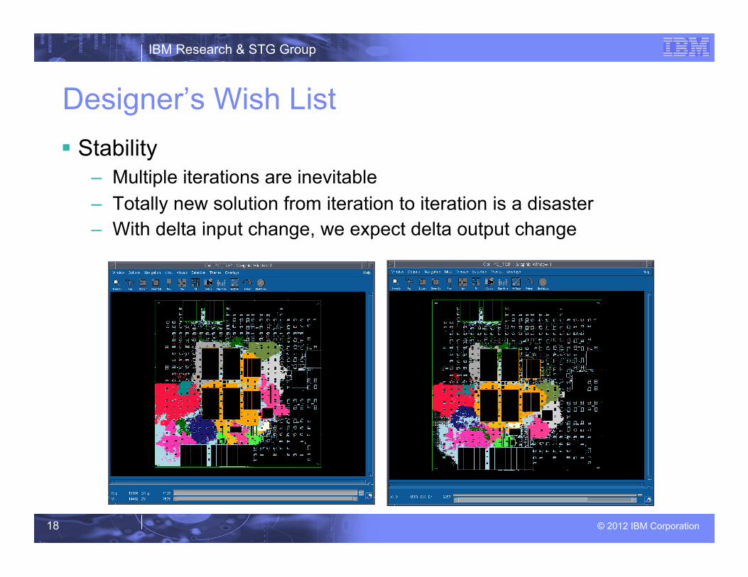
Designer’s Wish List Stability
– Multiple iterations are inevitable – Totally new solution from iteration to iteration is a disaster – With delta input change, we expect delta output change

IBM Research & STG Group
© 2012 IBM Corporation 19
Designer’s Wish List ECO friendly
– No surprise – Minimum perturbation to the current solution – Incomplete (infeasible) solution is better than no solution at all
IBM Research & STG Group
© 2012 IBM Corporation 20
Outline
Issues with 22nm design flow
Designer’s wish list
Fundamental techniques in timing closure – Courtesy of Paul Villarrubia, Chuck Alpert, Zhou Li, Shyam Ramji,
Natarajan Viswanathan, Cliff Sze and many folks from IBM EDA
Lithography-Aware Physical Synthesis (Top-down)
Co-Optimization of PD and DFM – Wire delay variability impact on PD optimization

IBM Research & STG Group
© 2012 IBM Corporation 21 21
PDS (Placement-Driven Synthesis) Timing Closure Flow
refine
Placement-Driven Optimization
Pre-processing
Congestion-driven placement
Early Optimization
Late Optimization
Timing-driven placement
place
Detailed Placement

IBM Research & STG Group
© 2012 IBM Corporation 22 22
Typical Timing Closure Tool
Eliminate iterations
Reduce Turn-Around-Time (TAT) Tight integration of relevant tools
– Floorplanning/Placement – Logic transforms to correct timing
– Gate Sizing
– Buffering – Logic restructuring
– Interconnection restructuring – Physical location change
– Routing – Congestion-aware
– Noise-aware

IBM Research & STG Group
© 2012 IBM Corporation 23 23
Placement
Input: a netlist of connected gates and nets
Output: exact locations of circuit elements Optimization: wire length, congestion, noise etc

IBM Research & STG Group
© 2012 IBM Corporation 24 24
Key Themes in Placement Placement problem consists of optimizing three orthogonal
components: – Relative order – Spacing – Global position
All in within the context of routability, timing and signal integrity
Placement within timing closure system is especially sensitive to stability

IBM Research & STG Group
© 2012 IBM Corporation 25 25
Analytical Partioning Placer vs. Force-directed Placer

IBM Research & STG Group
© 2012 IBM Corporation 26 26
Buffering: ITRS Projections

IBM Research & STG Group
© 2012 IBM Corporation 27 27
Simple Buffer Insertion Problem
Find: Buffer locations and a routing tree such that slack at the source, q(s0), is maximized
RAT2
RAT3 RAT4
RAT1
s0

IBM Research & STG Group
© 2012 IBM Corporation 28 28
Buffering Types High fanout buffering
Long net buffering

IBM Research & STG Group
© 2012 IBM Corporation 29 29
Gate Sizing
Size does matter
Bigger gate means smaller delay
Loop through all power levels
Find best slack without electrical violations
Del
ay o
f Pa
th
Gate Size
IBM Research & STG Group
© 2012 IBM Corporation 30
Outline
Issues with 22nm design flow
Designer’s wish list
Fundamental techniques in timing closure
Lithography-Aware Physical Synthesis (Top-down) – Litho/DFM enhanced Design Rules – DPT-enhanced routing – DPT-conflict removal (ICCAD 2011)
Co-Optimization of PD and DFM – Wire delay variability impact on PD optimization

IBM Research & STG Group
© 2012 IBM Corporation 31
Lithography-based Manufacturing Process

IBM Research & STG Group
© 2012 IBM Corporation 32
Lithography: Wavelength-based Scaling
Resolution (Minimum Pitch/2) = k1 λ
NA
NA
λ
365 nm 246 nm
193 nm
436 nm
Lithography resolution is given by a simple equation:
NA = numerical aperture = sine of largest diffracted angle captured by the lens. Not a good parameter for scaling:
• Lens manufacturing becomes hard at NA>.5 • depth-of-focus scales as 1/NA2
k1 = Rayleigh parameter = measure of lithography complexity, yield is affected at k1 < .65
For many generations, wavelength (λ) was the primary scaling parameter.
IBM Research & STG Group
© 2012 IBM Corporation 33
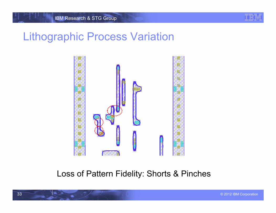
Lithographic Process Variation
Loss of Pattern Fidelity: Shorts & Pinches

IBM Research & STG Group
© 2012 IBM Corporation 34
Process Variations…….ahhhhh
249,403,263 Si atoms 68,743 donors 13,042 acceptors
D. J. Frank et al, Symp. VLSI Tech., 1999
IBM Research & STG Group
© 2012 IBM Corporation 35
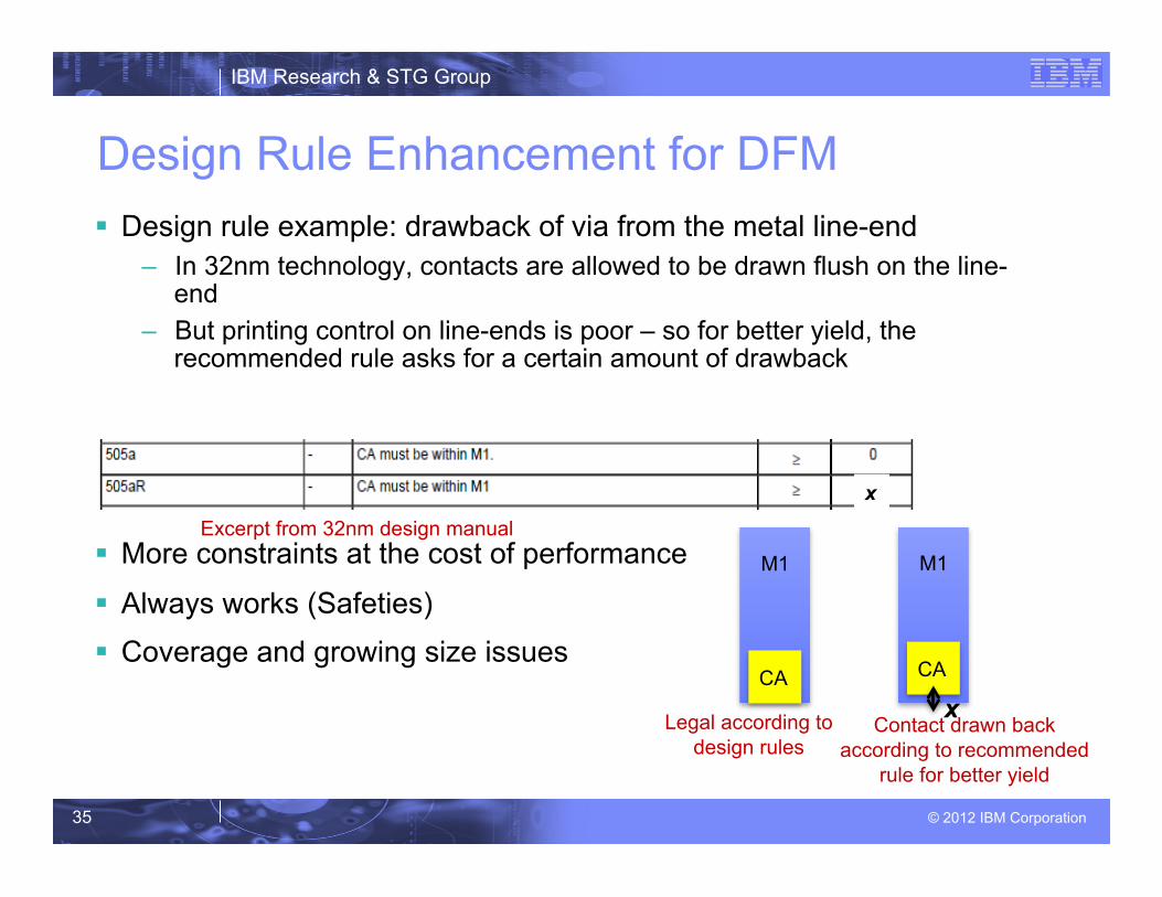
Design Rule Enhancement for DFM Design rule example: drawback of via from the metal line-end
– In 32nm technology, contacts are allowed to be drawn flush on the line-end
– But printing control on line-ends is poor – so for better yield, the recommended rule asks for a certain amount of drawback
More constraints at the cost of performance
Always works (Safeties) Coverage and growing size issues
Legal according to design rules
M1
CA
M1
CA
Contact drawn back according to recommended
rule for better yield
Excerpt from 32nm design manual
x
x

IBM Research & STG Group
© 2012 IBM Corporation 36
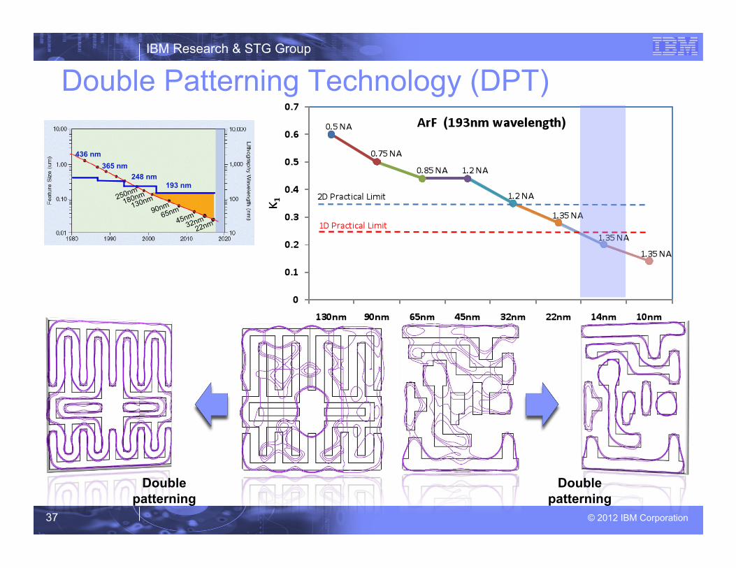
Double Patterning Technology (DPT)
C. Mack, IEEE Spectrum 08
IBM Research & STG Group
© 2012 IBM Corporation 37
Double Patterning Technology (DPT)
365 nm 248 nm
193 nm
436 nm
Double patterning
Double patterning

IBM Research & STG Group
© 2012 IBM Corporation 38
DPT-Enhanced Routing The most researched area in DPT-aware CAD tools
Mostly iterative method – Route/Check/Rip-up-Reroute for conflict removal – DPT-conflict is not necessarily local
Constructive phase solution starts to emerge – Design Rule-based one – Simultaneous routing/color assignment and stitch generation – Good recipe for ECO routing
IBM Research & STG Group
© 2012 IBM Corporation 39
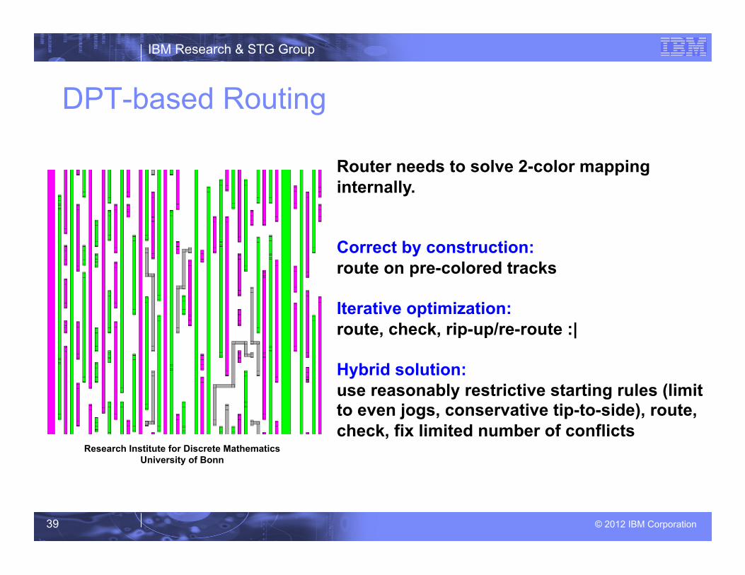
DPT-based Routing
Research Institute for Discrete Mathematics University of Bonn
Router needs to solve 2-color mapping internally.
Correct by construction: route on pre-colored tracks
Iterative optimization: route, check, rip-up/re-route :|
Hybrid solution: use reasonably restrictive starting rules (limit to even jogs, conservative tip-to-side), route, check, fix limited number of conflicts

IBM Research & STG Group
© 2012 IBM Corporation 40
DPT Conflict Resolution Framework
Double Patterning’s biggest challenge – Coloring conflicts
Stitching cannot resolve all conflicts
Odd cycle in post- stitching conflict graph native conflict
C. Mack, IEEE Spectrum 08
S"tch

IBM Research & STG Group
© 2012 IBM Corporation 41
Mask Assignment – Preferred coloring
Coloring of odd cycle affects efficiency of conflict removal
Give preference for opposite coloring for certain violations over others label violations critical vs. less-critical
– E.g., horizontal spacing violation more critical than vertical or diagonal in case of vertical poly orientation
Bad coloring Good coloring
M1 1st exposure M1 2nd exposure Na"ve conflict
Poly Ac"ve Contact

IBM Research & STG Group
© 2012 IBM Corporation 42
LP Formulation to Remove Conflicts
LP formulation allows fast polynomial time solving
Working with pre-colored layout – Allows legalization across multiple layers simultaneously – Solving conflict on one layer cannot create another elsewhere
Min layout perturba4on Problem formula4on:
DP rules

IBM Research & STG Group
© 2012 IBM Corporation 43
Conflict Removal Example
No conflicts, 6.2% area increase
Original 5 conflicts
Same area, 2 conflicts

IBM Research & STG Group
© 2012 IBM Corporation 44
Outline
Issues with 22nm design flow
Designer’s wish list
Fundamental techniques in timing closure
Lithography-Aware Physical Synthesis (Top-down)
Co-Optimization of PD and DFM – Wire delay variability impact on PD optimization
IBM Research & STG Group
© 2012 IBM Corporation 45
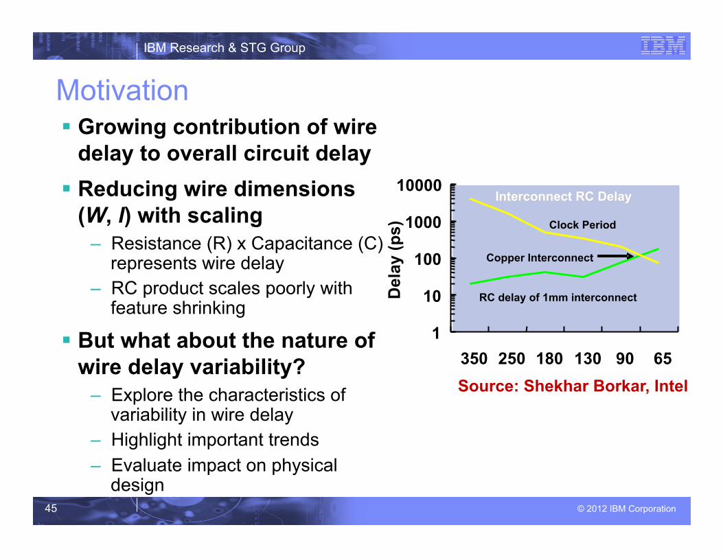
Motivation Growing contribution of wire
delay to overall circuit delay Reducing wire dimensions
(W, l) with scaling – Resistance (R) x Capacitance (C)
represents wire delay – RC product scales poorly with
feature shrinking
But what about the nature of wire delay variability?
– Explore the characteristics of variability in wire delay
– Highlight important trends – Evaluate impact on physical
design
Source: Shekhar Borkar, Intel
1
10
100
1000
10000
350 250 180 130 90 65
Del
ay (p
s)
Clock Period
RC delay of 1mm interconnect
Copper Interconnect

IBM Research & STG Group
© 2012 IBM Corporation 46
Wire Delay Models - 1 Resistance and capacitance can be modeled as functions
of wire dimensions Resistance per unit length Capacitance to ground plane per unit length (Sakurai et. al.
IEEE Trans. Elec. Devices 1983)
Separating out primary dimension of interest - wire width (W)

IBM Research & STG Group
© 2012 IBM Corporation 47
Wire Delay Models - 2 Capacitance to neighboring wire can be similarly written as
a function of width (W) and space (S)
Total capacitance is sum, so the total RC product can be similarly written as a function of width
IBM Research & STG Group
© 2012 IBM Corporation 48
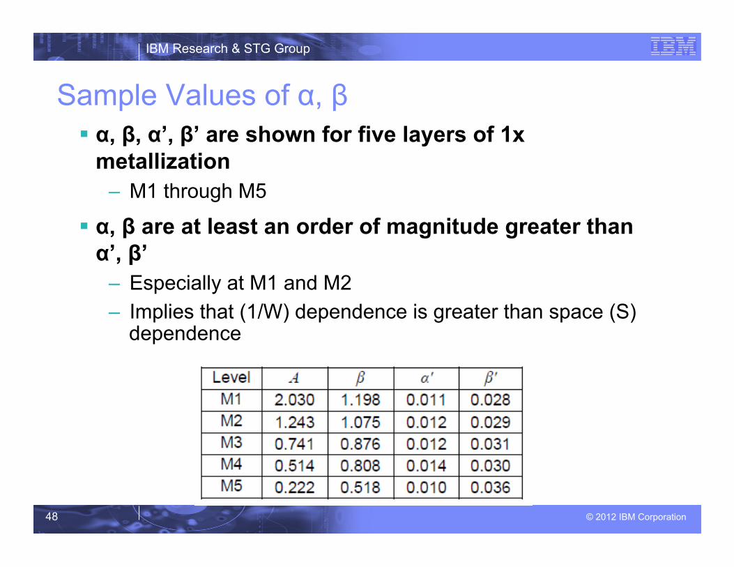
Sample Values of α, β α, β, α’, β’ are shown for five layers of 1x
metallization – M1 through M5
α, β are at least an order of magnitude greater than α’, β’
– Especially at M1 and M2 – Implies that (1/W) dependence is greater than space (S)
dependence

IBM Research & STG Group
© 2012 IBM Corporation 49
Wire Delay Sensitivity
α is wire RC delay per unit length when W is large
α, β are constants for a particular metal layer
Observation 1: Asymmetry of sensitivity of RC Delay
– To width variation around Wnom
– Small negative change in W has larger impact on RC than small positive change
Steep change in RC with W
Shallow change in RC with W
Sensi&vity of RC Delay to Wire Width
Delay of Wire with Neighbor vs. Width (from Simula&on)
IBM Research & STG Group
© 2012 IBM Corporation 50
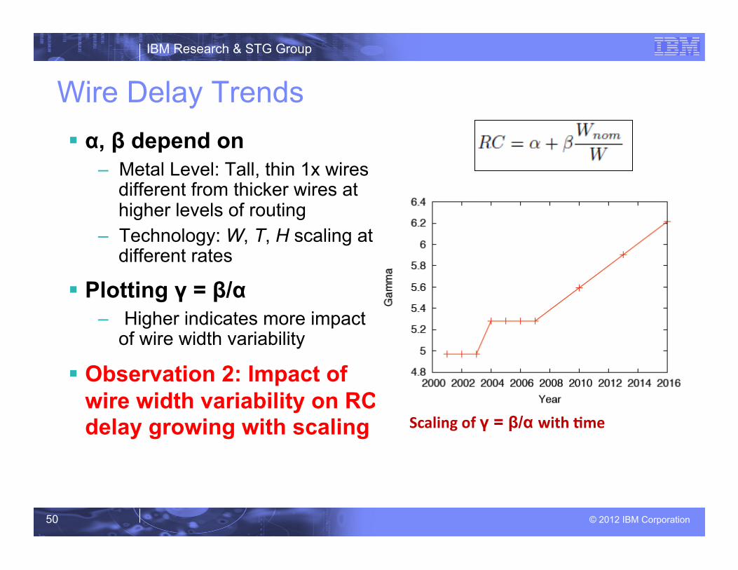
Wire Delay Trends α, β depend on
– Metal Level: Tall, thin 1x wires different from thicker wires at higher levels of routing
– Technology: W, T, H scaling at different rates
Plotting γ = β/α – Higher indicates more impact
of wire width variability
Observation 2: Impact of wire width variability on RC delay growing with scaling Scaling of γ = β/α with &me
IBM Research & STG Group
© 2012 IBM Corporation 51
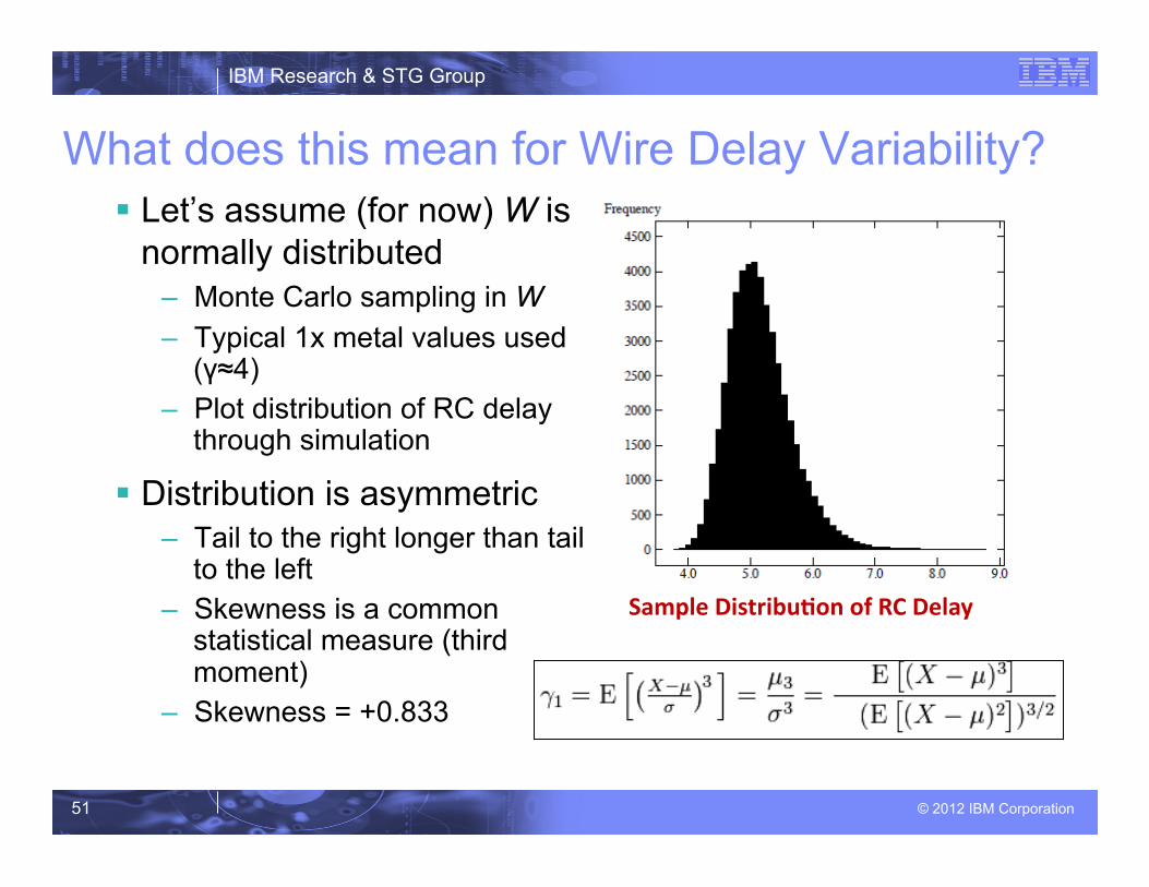
What does this mean for Wire Delay Variability? Let’s assume (for now) W is
normally distributed – Monte Carlo sampling in W – Typical 1x metal values used
(γ≈4) – Plot distribution of RC delay
through simulation
Distribution is asymmetric – Tail to the right longer than tail
to the left – Skewness is a common
statistical measure (third moment)
– Skewness = +0.833
Sample Distribu&on of RC Delay
IBM Research & STG Group
© 2012 IBM Corporation 52
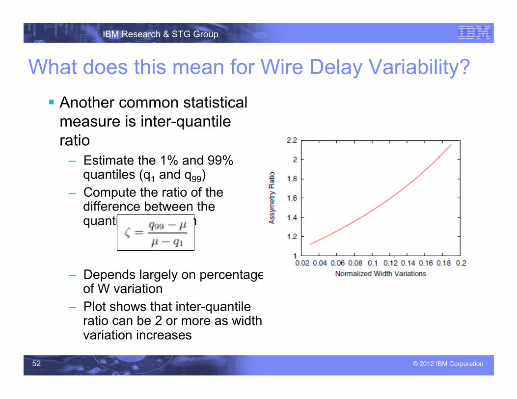
Another common statistical measure is inter-quantile ratio
– Estimate the 1% and 99% quantiles (q1 and q99)
– Compute the ratio of the difference between the quantiles and mean
– Depends largely on percentage of W variation
– Plot shows that inter-quantile ratio can be 2 or more as width variation increases
What does this mean for Wire Delay Variability?
IBM Research & STG Group
© 2012 IBM Corporation 53
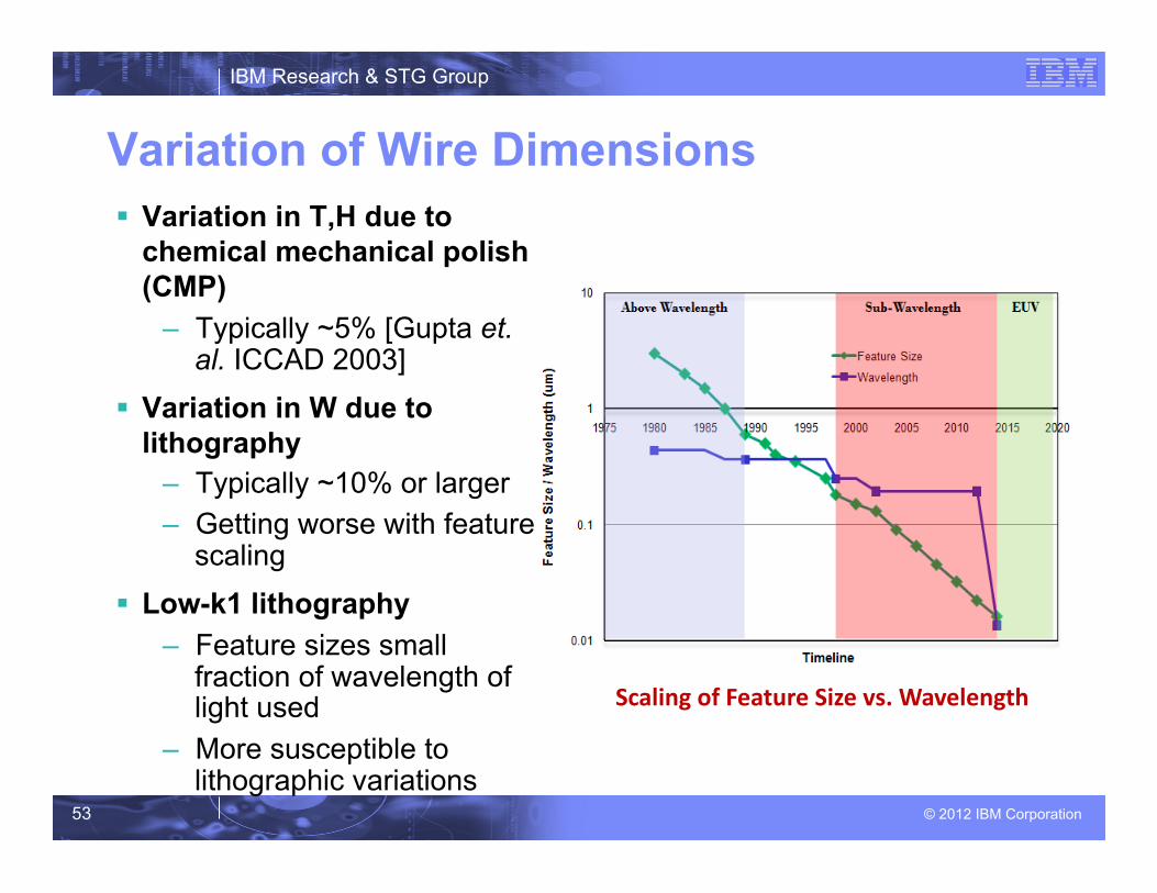
Variation of Wire Dimensions Variation in T,H due to
chemical mechanical polish (CMP)
– Typically ~5% [Gupta et. al. ICCAD 2003]
Variation in W due to lithography
– Typically ~10% or larger – Getting worse with feature
scaling Low-k1 lithography
– Feature sizes small fraction of wavelength of light used
– More susceptible to lithographic variations
Scaling of Feature Size vs. Wavelength

IBM Research & STG Group
© 2012 IBM Corporation 54
Variation of Wire Width Due to Lithography Primary sources of
lithographic variation – Dose errors – Focus errors – Mask / overlay errors
Impact of dose on width is approximately linear [Smith et. al. SPIE 2002]
Impact of focus on width is parabolic in nature
– Manufacturing data fitted to parabolic function
Impact of Dose and Focus Varia&ons on Wire Width

IBM Research & STG Group
© 2012 IBM Corporation 55
Impact of Lithography on RC Variation Dose and focus can be
assumed to be approximately normally distributed
– Central limit theorem – Zero mean Gaussian
processes
Wire width distribution – Monte Carlo sampling in dose/
focus space Observation 3: Lithographic
variations push RC delay distribution towards further asymmetry
0 200 400 600 800
1000 1200 1400 1600 1800 2000
0.04
4
0.04
55
0.04
7
0.04
85
0.05
0.05
15
0.05
3
Freq
uenc
y Width Bin (normalized)
Wire Width Distribution

IBM Research & STG Group
© 2012 IBM Corporation 56
Impact of Lithography on RC Variation - 2 RC histogram for typical range of
dose/focus variations Assumed different ranges of
defocus in the process – Inter-quantile ratio plotted – Shows that amount of skew in
RC distribution very quickly increases as focus gets out of control
Inter-quantile Ratio as function of Range of Defocus
0
200
400
600
800
1000
1200
0.98
0.986
0.992
0.998
1.004
1.01
1.016
1.022
1.028
1.034
1.04
Freq
uenc
y
RC Bin (normalized)
Considering Gaussian W
Manfuactured (Regular OPC)

IBM Research & STG Group
© 2012 IBM Corporation 57
What does this mean for Physical Design?
Hold (H) and setup (S) time constraints
– Defined by late arrival time (∆) and early arrival (δ) time
Most current methodologies consider only nominal wire delay during timing
– But M3 1x wire can be 2% slow or 21% fast equally likely!
– Introduced new terms for interconnect delay ∆ILate and δIFast

IBM Research & STG Group
© 2012 IBM Corporation 58
Timing Analysis with Wire Delay Asymmetry Late mode timing analysis on sample 32nm ASIC macros
with wire delay asymmetry accounted for – Compared against no wire delay variability (only nominal wire
delay) – Total negative slack (TNS) increases by ~15% – Total number of paths with negative slack increases by ~12% – Paths would have been undetected as causing timing failures if
only nominal wire delay was considered
IBM Research & STG Group
© 2012 IBM Corporation 59
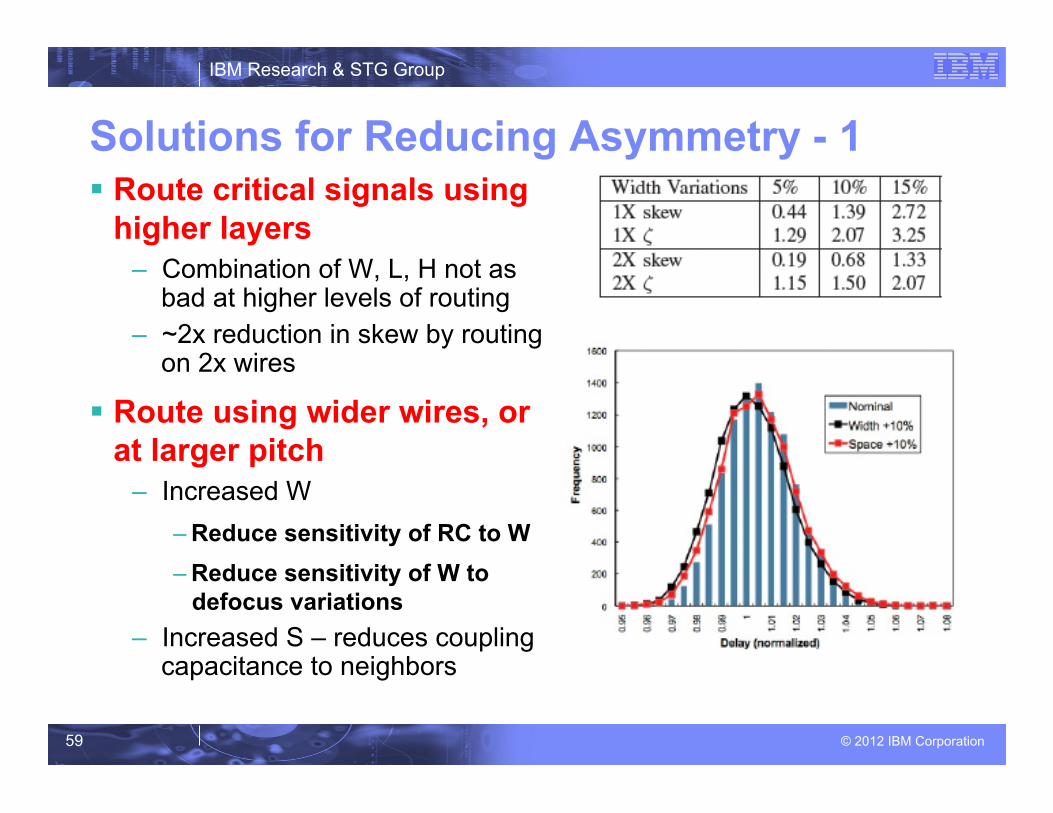
Solutions for Reducing Asymmetry - 1 Route critical signals using
higher layers – Combination of W, L, H not as
bad at higher levels of routing – ~2x reduction in skew by routing
on 2x wires Route using wider wires, or
at larger pitch – Increased W
– Reduce sensitivity of RC to W – Reduce sensitivity of W to
defocus variations – Increased S – reduces coupling
capacitance to neighbors
IBM Research & STG Group
© 2012 IBM Corporation 60
0
200
400
600
800
1000
1200
1400
0.96 0.98 1 1.02 1.04 1.06
Freq
uenc
y
RC Delay (normalized)
Manfuactured (Defocus OPC)
Manfuactured (Regular OPC)
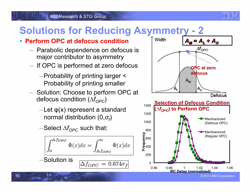
Solutions for Reducing Asymmetry - 2 Perform OPC at defocus condition
– Parabolic dependence on defocus is major contributor to asymmetry
– If OPC is performed at zero defocus – Probability of printing larger <
Probability of printing smaller – Solution: Choose to perform OPC at
defocus condition (∆fOPC) – Let φ(x) represent a standard
normal distribution (0,σf)
– Select ∆fOPC such that:
– Solution is
Selection of Defocus Condition (∆fOPC) to Perform OPC
OPC at zero defocus

IBM Research & STG Group
© 2012 IBM Corporation 61
Conclusion Need to worry about wire delay variability in addition to magnitude Demonstrated the asymmetric nature of wire delay variability
– Skewness increasing with scaling Highlighted three major contributing factors
– Sensitivity of delay to smaller wire widths in current technologies – Increase of this sensitivity with scaling – Skewed variation of wire width itself due to lithographic variations
Demonstrated impact on timing analysis – Not considering wire delay variability can lead to ~12% more failing paths
Evaluated techniques to reduce delay asymmetry – Design methods – route at higher levels, route using wider wires – Manufacturing method – perform OPC at defocus condition

IBM Research & STG Group
© 2012 IBM Corporation 62
Summary Lithography issue will affect design process in 20nm and
beyond – Current practice is rather ad-hoc with bunch of heuristics mostly
at post-design stage
Co-optimization is desirable – Litho-aware design optimization – Design-aware litho optimization
Minimum perturbation-based optimization is important – No further source of late surprise