bridging the gap between digital circuits and microprocessors
TRANSCRIPT
334 IEEE TRANSACTIONS ON EDUCATION, VOL. 36, NO. 3, AUGUST 1993
Bridging the Gap Between Digital Circuits and Microprocessors
John D. Carpinelli, Senior Member, IEEE, and Sol Rosenstark, Senior Member, IEEE
Abstruct- Most electrical and computer engineering students understand digital circuits and microprocessors, but fail to appre- ciate that a microprocessor is just a complex finite state machine. This paper presents a three experiment sequence which takes the
from the design of a simple EEPROM-based finite state machine through a two chip microsequencer to a 4-bit central processing unit.
The remainder of this paper is organized as follows. Section 11 describes the finite state machine experiment. It gives the background in a manner similar to that shown in the laboratory manual, a description of the experiment and student OutCOmeS. Sections 111 and I v describe the two chip miCrOSeqUellCer and the 4-bit central processing unit experiments in a similar format. Conclusions are presented in Section V.
1. INTRODUCTION 11. FINITE STATE MACHINE
T is very instructive for students who have taken a course I in computer architecture to perform some experiments which allow them the first-hand experience of building a microprogrammed central processing unit (CPU). There are many approaches to this undertaking. One method [l] is to have students implement a fairly complicated design based on SSI or MSI circuits. The complexity of this method precludes the students from actually building the CPU. Instead, they study the behavior of the prospective CPU on a simulator. In other experiments [2 ] , [3], the students write and debug CPU microcode. This is then verified on a commercially available board.
Many students think of digital circuits and microprocessors as distinct topics, when in fact microprocessors are just com- plex finite state machines. The microprocessor is the result of advances in the design and implementation of large digital circuits. This paper describes a sequence of three experiments which take the student from the design of a simple finite state machine through the design and implementation of a 4- bit central processing unit. The experiments were deliberately made sufficiently simple to allow the students to implement the design and perform tests to see if specifications are met. Nevertheless, the simplicity of the experiments does not in any way detract from the students’ understanding of microprocessor design. In the process, the students also gain an understanding of the use of programmable logic devices in the implementation of digital logic design.
The experiments are part of the laboratory course for first semester senior computer engineering students [4]. A computer architecture course is a corequisite to the lab [5 ] . Prior to the course, the students have taken a one semester course in digital circuits, a one semester course in microprocessors and one laboratory course in each area.
Manuscript received April 1992. The authors are with the Department of Electrical and Computer Engi-
neering, New Jersey Institute of Technology, University Heights, Newark, NJ 07102.
IEEE Log Number 9209813.
A. Background
Event driven sequential circuits differ from combinatorial circuits in that the outputs of the circuit depend not only on the present state of the inputs but also on the past history of the inputs. Thus, a sequential circuit has memory. Memory is provided for each bit needed to define a state by using a bit storage device such as a flip-flop. The combinatorial part of the circuit can be implemented using gates, multiplexers or any method that is capable of providing the necessary feedback logic. In this case, an EEPROM is used. The storage device used is an octal D-type latch; the entire design has a chip count of two.
In this experiment an event driven sequential circuit is implemented. This type of circuit is free running in the sense that the output must respond to an input change in a very short time. It is clearly the input change which drives the circuit, so the circuit is called event driven.
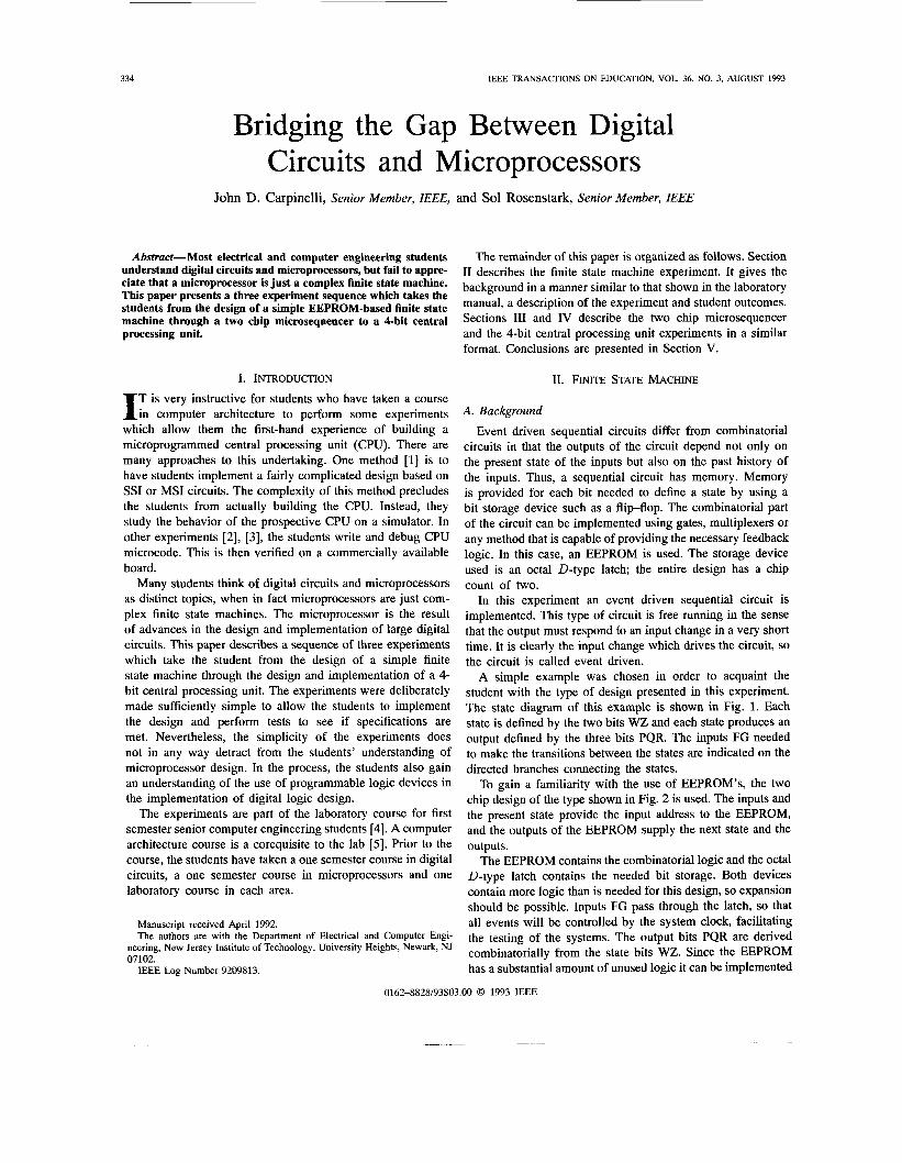
A simple example was chosen in order to acquaint the student with the type of design presented in this experiment. The state diagram of this example is shown in Fig. 1. Each state is defined by the two bits WZ and each state produces an output defined by the three bits PQR. The inputs FG needed to make the transitions between the states are indicated on the directed branches connecting the states.
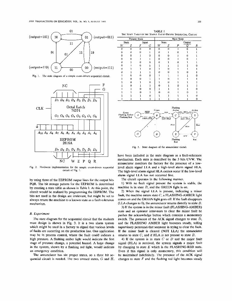
To gain a familiarity with the use of EEPROM’s, the two chip design of the type shown in Fig. 2 is used. The inputs and the present state provide the input address to the EEPROM, and the outputs of the EEPROM supply the next state and the outputs.
The EEPROM contains the combinatorial logic and the octal D-type latch contains the needed bit storage. Both devices contain more logic than is needed for this design, so expansion should be possible. Inputs FG pass through the latch, so that all events will be controlled by the system clock, facilitating the testing of the systems. The output bits PQR are derived combinatorially from the state bits WZ. Since the EEPROM has a substantial amount of unused logic it can be implemented
0162-8828/93$03.00 0 1993 IEEE
IEEE TRANSACTIONS ON EDUCATION, VOL. 36, NO. 3, AUGUST 1993 335
Present State - State - Input
W Z F G W Z P
0 0 0
0 0 1
0 1 0 1 1 1 0 1 1 0 1 1 1 0 0 0 1 1
1 0 1 1 1 0 0 1 1 1 1 0 1 1 1 0 1 1
00
Next State - State output -
Q R 0 0 0 0 0 0 1 0 1
1 0 1 0 1 1 0 0 1 0 0 0 1 0 1
1 0 0 1 0 1 0 1 0 0 0 1 0 1 1
1 1 0 0 1 0 1 1 1 1 0 0 1 0 1
1 1 0 1 0 0 1 1 0 1 1 1 1 0 1 0 1 0 1 1 1
1 0 1 0 1 1 1 1 0
1 0 0 1 0 1 1 1 0
Fig. 1. The state diagram of a simple event-driven sequential circuit.
CLK i Octal Latch 74374
EEPROM 2816A l l I
0 7 D6 0 5 0 4 0 3 D2 Di Do 1 NC W Z P Q R
U r ! ! ! ! I l l
Fig. 2. Hardware implementation for the simple event-driven sequential circuit of Fig. 1.
by using three of the EEPROM output lines for the output bits PQR. The bit storage pattern for the EEPROM is determined by creating a state table as shown in Table 1. At this point, the circuit would be realized by programming the EEPROM. The bits not used in the design are irrelevant, but might be set to always retum the machine to a known state as a fault-tolerance mechanism.
B. Experiment
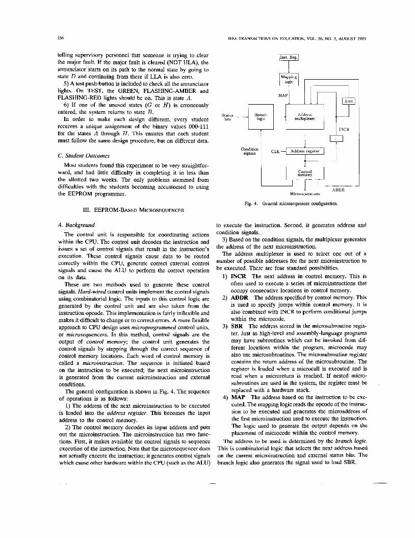
The state diagram for the sequential circuit that the students must design is shown in Fig. 3. It is a two alarm system which might be used in a factory to signal that various levels of faults are occurring on the production line. One application may be in process control, where the fault could indicate a high pressure. A flashing amber light would indicate the first stage of pressure change, a potential hazard. A large change in the system, shown by a flashing red light, would indicate an emergency condition.
The annunciator has six proper states, so a three bit se- quential circuit is needed. The two unused states, G and H ,
1 1 1 1 1 1 1 1 1 0
Flashing
Green Flashing Amber
Flashing Red
Amher- Amber
HLA
F E ACK G H
Flashing Red Red
Fig. 3. State diagram of the annunciator circuit.
have been included in the state diagram as a fault-tolerance mechanism. Each state is described by the 3 bits UVW. The annunciator monitors the factory for the presence of a low- level alarm signal LLA and a high-level alarm signal HLA. The high-level alarm signal HLA cannot occur if the low-level alarm signal LLA has not occurred first.
The circuit operates in the following manner. 1) With no fault signal present the system is stable, the
machine is in state B, and the GREEN light is on. 2) When the signal LLA is present, indicating a minor
fault, the machine enters state C, a FLASHING-AMBER light comes on and the GREEN light goes off. If the fault disappears (LLA changes to 0), the annunciator returns directly to state B.
3) If the system is in the minor fault (FLASHING-AMBER) state and an operator intervenes to clear the minor fault he pushes the acknowledge button which contains a momentary switch. The presence of the ACK signal changes to state D, and the FLASHING AMBER light becomes steady, telling supervisory personnel that someone is trying to clear the fault. If the minor fault is cleared (NOT LLA) the annunciator returns to state C, and if HLA is not present to state B.
4) If the system is in state C or D and the major fault signal (HLA) is received, the system signals a major fault by changing to state E which is the FLASHING-RED state. Even if this signal is only momentary, this condition will be maintained indefinitely. The presence of the ACK signal changes to state F and the flashing red light becomes steady
336
-
IEEE TRANSACTIONS ON EDUCATION, VOL. 36, NO. 3, AUGUST 1993
Branch Address logic -
telling supervisory personnel that someone is trying to clear the major fault. If the major fault is cleared (NOT HLA), the annunciator starts on its path to the normal state by going to state D and continuing from there if LLA is also zero.
5) A test push-button is included to check all the annunciator lights. On TEST, the GREEN, FLASHING-AMBER and FLASHING-RED lights should be on. This is state A .
6) If one of the unused states (G or H ) is erroneously entered, the system returns to state B.
In order to make each design different, every student receives a unique assignment of the binary values 000-1 11 for the states A through H . This ensures that each student must follow the same design procedure, but on different data.
C. Student Outcomes
Most students found this experiment to be very straightfor- ward, and had little difficulty in completing it in less than the allotted two weeks. The only problems stemmed from difficulties with the students becoming accustomed to using the EEPROM programmer.
111. EEPROM-BASED MICROSEQUENCER
A. Background
The control unit is responsible for coordinating actions within the CPU. The control unit decodes the instruction and issues a set of control signals that result in the instruction's execution. These control signals cause data to be routed correctly within the CPU, generate correct external control signals and cause the ALU to perform the correct operation on its data.
These are two methods used to generate these control signals. Hard-wired control units implement the control signals using combinatorial logic. The inputs to this control logic are generated by the control unit and are also taken from the instruction opcode. This implementation is fairly inflexible and makes it difficult to change or to correct errors. A more flexible approach to CPU design uses microprogrammed control units, or microsequencers. In this method, control signals are the output of control memory; the control unit generates the control signals by stepping through the correct sequence of control memory locations. Each word of control memory is called a microinstruction. The sequence is initiated based on the instruction to be executed; the next microinstruction is generated from the current microinstruction and external conditions.
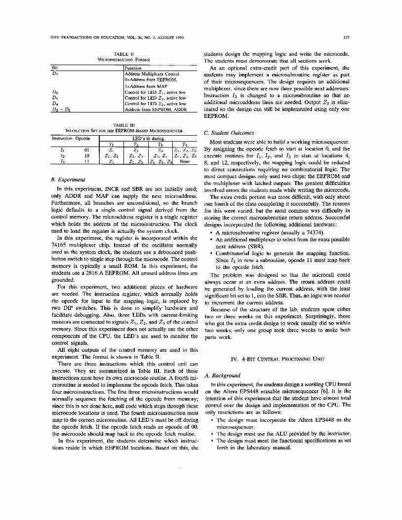
The general configuration is shown in Fig. 4. The sequence of operations is as follows:
1) The address of the next microinstruction to be executed is loaded into the address register. This becomes the input address to the control memory.
2) The control memory decodes its input address and puts out the microinstruction. The microinstruction has two func- tions. First, it makes available the control signals to sequence execution of the instruction. Note that the microsequencer does not actually execute the instruction; it generates control signals which cause other hardware within the CPU (such as the ALU)
Status - bits
I
Condition signals
Fig. 4.
I-' I INCR
CLK
Control memory
Micro-operations
General microsequencer configuration.
to execute the instruction. Second, it generates address and condition signals.
3) Based on the condition signals, the multiplexer generates the address of the next microinstruction.
The address multiplexer is used to select one out of a number of possible addresses for the next microinstruction to be executed. There are four standard possibilities.
1) INCR The next address in control memory. This is often used to execute a series of microinstructions that occupy consecutive locations in control memory.
2) ADDR The address specified by control memory. This is used to specify jumps within control memory. It is also combined with INCR to perform conditional jumps within the microcode.
3) SBR The address stored in the microsubroutine regis- ter. Just as high-level and assembly-language programs may have subroutines which can be invoked from dif- ferent locations within the program, microcode may also use microsubroutines. The microsubroutine register contains the return address of the microsubroutine. The register is loaded when a microcall is executed and is read when a microreturn is reached. If nested micro- subroutines are used in the system, the register must be replaced with a hardware stack.
The address based on the instruction to be exe- cuted. The mapping logic reads the opcode of the instruc- tion to be executed and generates the microaddress of the first microinstruction used to execute the instruction. The logic used to generate the output depends on the placement of microcode within the control memory.
The address to be used is determined by the branch logic. This is combinatorial logic that selects the next address based on the current microinstruction and external status bits. The branch logic also generates the signal used to load SBR.
4) MAP
IEEE TRANSACTIONS ON EDUCATION, VOL. 36, NO. 3, AUGUST 1993
Bit D7
D6 D5 D4 D3 - Do
337
Function Address Multiplexer Control O=Address from EEPROM, l=Address from MAP Control for LED Z1, active low Control for LED 2 2 , active low Control for LED Z3, active low Address from EEPROM, ADDR
TABLE 111 INSTRUCTION SET FOR THE EEPROM-BASED MICROSEQUENCER
Instruction Opcode LED’s lit durin
I2 10 11
B. Experiment
In this experiment, INCR and SBR are not initially used; only ADDR and MAP can supply the next microaddress. Furthermore, all branches are unconditional, so the branch logic defaults to a single control signal derived from the control memory. The microaddress register is a single register which holds the address of the microinstruction. The clock used to load the register is actually the system clock.
In this experiment, the register is incorporated within the 74165 multiplexer chip. Instead of the oscillator normally used as the system clock, the students use a debounced push- button switch to single step through the microcode. The control memory is typically a small ROM. In this experiment, the students use a 2816 A EEPROM. All unused address lines are grounded.
For this experiment, two additional pieces of hardware are needed. The instruction register, which normally holds the opcode for input to the mapping logic, is replaced by two DIP switches. This is done to simplify hardware and facilitate debugging. Also, three LEDs with current-limiting resistors are connected to signals 21, 22, and Z3 of the control memory. Since this experiment does not actually use the other components of the CPU, the LED’s are used to monitor the control signals.
All eight outputs of the control memory are used in this experiment. The format is shown in Table 11.
There are three instructions which this control unit can execute. They are summarized in Table 111. Each of these instructions must have its own microcode routine. A fourth mi- croroutine is needed to implement the opcode fetch. This takes four microinstructions. The first three microinstructions would normally sequence the fetching of the opcode from memory; since this is not done here, null code which steps through these microcode locations is used. The fourth microinstruction must map to the correct microroutine. All LED’s must be off during the opcode fetch. If the opcode fetch reads an opcode of 00, the microcode should map back to the opcode fetch routine.
In this experiment, the students determine which instruc- tions reside in which EEPROM locations. Based on this, the
students design the mapping logic and write the microcode. The students must demonstrate that all sections work.
As an optional extra-credit part of this experiment, the students may implement a microsubroutine register as part of their microsequencers. The design requires an additional multiplexer, since there are now three possible next addresses. Instruction 13 is changed to a microsubroutine so that no additional microaddress lines are needed. Output 2 3 is elim- inated so the design can still be implemented using only one EEPROM.
C. Student Outcomes
Most students were able to build a working microsequencer. By assigning the opcode fetch to start at location 0, and the execute routines for I I , 12, and I3 to start at locations 4, 8, and 12, respectively, the mapping logic could be reduced to direct connections requiring no combinatorial logic. The most compact designs only used two chips: the EEPROM and the multiplexer with latched outputs. The greatest difficulties involved errors the students made while writing the microcode.
The extra credit portion was more difficult, with only about one fourth of the class completing it successfully. The reasons for this were varied, but the most common was difficulty in storing the correct microsubroutine return address. Successful designs incorporated the following additional hardware:
A microsubroutine register (usually a 74374). An additional multiplexer to select from the extra possible next address (SBR). Combinatorial logic to generate the mapping function. Since I3 in now a subroutine, opcode 11 must map back to the opcode fetch.
The problem was designed so that the microcall could always occur at an even address. The return address could be generated by loading the current address, with the least significant bit set to 1, into the SBR. Thus, no logic was needed to increment the current address.
Because of the structure of the lab, students spent either two or three weeks on this experiment. Surprisingly, those who got the extra credit design to work usually did so within two weeks; only one group took three weeks to make both parts work.
IV. 4-BIT CENTRAL PROCESSING UNIT
A. Background In this experiment, the students design a working CPU based
on the Altera EPS448 erasable microsequencer [6]. It is the intention of this experiment that the student have almost total control over the design and implementation of the CPU. The only restrictions are as follows:
The design must incorporate the Altera EPS448 as the microsequencer. The design must use the ALU provided by the instructor. The design must meet the functional specifications as set forth in the laboratory manual.
338
0 1 1
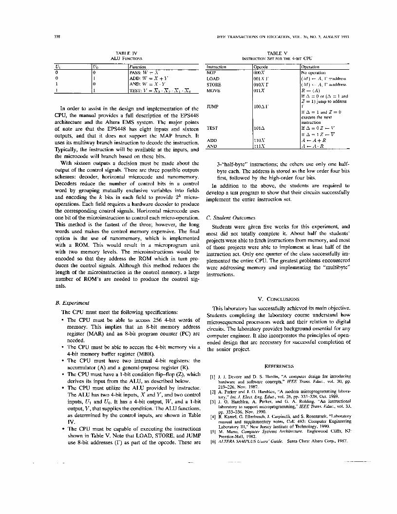
TABLE IV &U FUNCTIONS
1 A D D : W = X + k ’ 0 AND: W = X . Y 1 T E S T V = X g . X 2 . x l . X O
IEEE TRANSACTIONS ON EDUCATION, VOL. 36, NO. 3, AUGUST 1993
TABLE V INSTRUCTION SET FOR THE 4-BIT CPU
U1 I U0 I Function 0 Io IPASS: W = X
In order to assist in the design and implementation of the CPU, the manual provides a full description of the EPS448 architecture and the Altera EMS system. The major points of note are that the EPS448 has eight inputs and sixteen outputs, and that it does not support the M A P branch. It uses its multiway branch instruction to decode the instruction. Typically, the instruction will be available at the inputs, and the microcode will branch based on these bits.
With sixteen outputs a decision must be made about the output of the control signals. There are three possible outputs schemes: decoder, horizontal microcode and nanomemory. Decoders reduce the number of control bits in a control word by grouping mutually exclusive variables into fields and encoding the k bits in each field to provide 2k micro- operations. Each field requires a hardware decoder to produce the corresponding control signals. Horizontal microcode uses one bit of the microinstruction to control each micro-operation. This method is the fastest of the three; however, the long words used makes the control memory expensive. The final option is the use of nanomemory, which is implemented with a ROM. This would result in a microprogram unit with two memory levels. The microinstructions would be encoded so that they address the ROM which in turn pro- duces the control signals. Although this method reduces the length of the microinstruction in the control memory, a large number of ROM’s are needed to produce the control sig- nals.
B. Experiment
The CPU must meet the following specifications: The CPU must be able to access 256 4-bit words of memory. This implies that an 8-bit memory address register (MAR) and an 8-bit program counter (PC) are needed. The CPU must be able to access the 4-bit memory via a 4-bit memory buffer register (MBR). The CPU must have two internal 4-bit registers: the accumulator (A) and a general-purpose register (R). The CPU must have a 1-bit condition flip-flop (Z), which derives its input from the ALU, as described below. The CPU must utilize the ALU provided by instructor. The ALU has two 4-bit inputs, X and Y , and two control inputs, U1 and UO. It has a 4-bit output, W , and a 1-bit output, V, that supplies the condition. The ALU functions, as determined by the control inputs, are shown in Table IV. The CPU must be capable of executing the instructions shown in Table V. Note that LOAD, STORE, and JUMP use 8-bit addresses (I?) as part of the opcode. These are
Instruction NOP LOAD STORE MOVE
JUMP
TEST
ADD AND
3pcode IOOX ioix r ]lox r 111x
~ O O A r
lOlA
l l 0 X l l l X
Operation No operation ( M ) t A, r =address ( M ) t A, r =address
If A = 0 or (A = 1 and 2 = 1) jump to address
If A = 1 and Z = 0 execute the next instruction If A = 0 Z t I’ If A = 12 t v A t A + R
€3 ( A )
r
A t A . R
3-“half-byte” instructions; the others use only one half- byte each. The address is stored as the low order four bits first, followed by the high-order four bits.
In addition to the above, the students are required to develop a test program to show that their circuits successfully implement the entire instruction set.
C. Student Outcomes Students were given five weeks for this experiment, and
most did not totally complete it. About half the students’ projects were able to fetch instructions from memory, and most of those projects were able to implement at least half of the instruction set. Only one quarter of the class successfully im- plemented the entire CPU. The greatest problems encountered were addressing memory and implementing the “multibyte” instructions.
V. CONCLUSIONS
This laboratory has successfully achieved its main objective. Students completing the laboratory course understand how microsequenced processors work and their relation to digital circuits. The laboratory provides background essential for any computer engineer. It also incorporates the principles of open- ended design that are necessary for successful completion of the senior project.
REFERENCES
[ l ] J. J. Devore and D. S. Hardin, “A computer design for introducing hardware and software concepts,” IEEE Trans. Educ., vol. 30, pp. 219-226, Nov. 1987.
[2] A. Parker and J. 0. Hamblen, “A modem microprogramming labora- tory,” Inr. J . Elect. Eng. Educ., vol. 26, pp. 333-338, Oct. 1989.
[3] J. 0. Hamblen, A. Parker, and G. A. Rohling, “An instructional laboratory to support microprogramming,” IEEE Trans. Educ., vol. 33, pp. 333-336, Nov. 1990.
[4] R. Kamel, G. Ellerbusch, J. Carpinelli, and S. Rosenstark, “Laboratory manual and supplementary notes, CoE 493: Computer Engineering Laboratory 111,” New Jersey Institute of Technology, 1990.
Englewood Cliffs, NJ: Prentice-Hall, 1982.
[5] M. Mano, Computer Systems Architecture.
[6] ALTERA SAMPLUS Users’ Guide. Santa Clara: Altera Corp., 1987.
IEEE TRANSACTIONS ON EDUCATION, VOL. 36, NO. 3, AUGUST 1993 339
John D. Carpinelli (SM’93) received the B.E. degree in electrical engineering from Stevens In- stitute of Technology, in 1983, and the M.E. degree in electrical engineering and the Ph.D. degree in computer and systems engineering from Rensselaer Polytechnic Institute, NY, in 1984 and 1987, re- spectively.
In 1986, he joined the Department of Electrical and Computer Engineering at the New Jersey Insti- tute of Technology, Newark, where he is currently an Associate Professor and the Associate Director
of the Computer Engineering program. His primary research interests include computers in education, interconnection networks, and biomedical computing.
Dr. Carpinelli is a member of the IEEE Computer and Education Societies.
Sol Rosenstark (SM’93) received the B.E.E. degree from the City College of New York, NY, in 1958, and the M.E.E. and Ph.D. degrees from New York University, NY, in 1961 and 1966, respectively.
He has held industrial positions of Associate Development Engineer in Theoretical Analysis of Stable Platform Inertial Navigation Guidance Sys- tems at Norden Laboratories, in Nonvalk, CT, and also that of Member of Technical Staff in the High Speed Digital Transmission Laboratory, at Bell Telephone Laboratories, Holmdel, NJ. In the
academic world, he has served as Lecturer in Electrical Engineering at the City College of New York, and from 1968, he has been with the Electrical and Computer Engineering Department at the New Jersey Institute of Technology. Professor Rosenstark has worked in Communications Theory with special interest in the areas of Spread Spectrum Communication Systems and in Command Control and Communication Systems Analysis. He has also had a continuing interest in clarifying the theory of Feedback Amplifiers, and has published papers in this field, as well as the textbook Feedback Amplifier Principles, published by Macmillan in 1986.
Dr. Rosenstark has been actively involved with Microprocessors and Microcomputers. He has taught and consulted in this area. Recently, he has also taken a strong interest in the interconnection of digital devices. He is a member of Eta Kappa Nu, and Sigma Xi. He is a registered professional engineer in the state of New York.