bq27510-g3 system-side impedance track fuel gauge … · host system pack-single-cell li-ion...
TRANSCRIPT

Host System
PACK-
Single-Cell Li-ionBattery Pack
CHG
DSG
TempSense
CurrentSense
T
PACK+
VoltageSenseGPOUT
FETs
I C2
LDOREG25 REGIN
VCC
DATA
bq27510-G3
PowerManagement
Controller
PROTECTION
IC
Product
Folder
Sample &Buy
Technical
Documents
Tools &
Software
Support &Community
bq27510-G3SLUSAT1A –MARCH 2013–REVISED NOVEMBER 2015
bq27510-G3 System-Side Impedance Track™ Fuel Gauge With Direct Battery Connection1 Features 2 Applications1• Single-Series Cell Li-Ion Battery Fuel Gauge • Smartphones, Feature Phones, and Tablets
Resides on System Board • Wearables– Integrated 2.5-VDC LDO • Building Automation– External Low-Value 10-mΩ Sense Resistor • Portable Medical/Industrial Handsets
• Patented Impedance Track™ Technology • Portable Audio– Adjusts for Battery Aging, Self-Discharge, • Gaming
Temperature, and Rate Changes3 Description– Reports Remaining Capacity, State-of-Charge
(SOC), and Time-to-Empty The Texas Instruments bq27510-G3 system-side Li-Ion battery fuel gauge is a microcontroller peripheral– Optional Smoothing Filterthat provides fuel gauging for single-cell Li-Ion battery– Battery State-of-Health (Aging) Estimation packs. The device requires little system
– Supports Embedded or Removable Packs microcontroller firmware development. The bq27510-With up to 32-Ahr Capacity G3 resides on the system’s main board and manages
an embedded battery (non-removable) or a– Accommodates Pack Swapping With 2removable battery pack.Separate Battery ProfilesThe bq27510-G3 uses the patented Impedance• Microcontroller Peripheral Supports:Track™ algorithm for fuel gauging, and provides– 400-kHz I2C Serial Interface information such as remaining battery capacity
– 32 Bytes of Scratch-Pad FLASH NVM (mAh), state-of-charge (%), run-time to empty (min.),battery voltage (mV), temperature (°C) and state-of-– Battery Low Digital Output Warninghealth (%).– Configurable SOC InterruptsBattery fuel gauging with the bq27510-G3 requires– External Thermistor, Internal Sensor, or Host-only PACK+ (P+), PACK– (P–), and optionalReported Temperature OptionsThermistor (T) connections to a removable battery• Small 12-Pin 2.50 mm × 4.00 mm SON Package pack or embedded battery circuit.
Device Information(1)
FIRMWAREPART NUMBER PACKAGE VERSIONbq27510-G3 SON (12) 4.00 (0X0400)
(1) For all available packages, see the orderable addendum atthe end of the data sheet.
Typical Application Diagram
1
An IMPORTANT NOTICE at the end of this data sheet addresses availability, warranty, changes, use in safety-critical applications,intellectual property matters and other important disclaimers. PRODUCTION DATA.

bq27510-G3SLUSAT1A –MARCH 2013–REVISED NOVEMBER 2015 www.ti.com
Table of Contents7.3 Feature Description................................................. 101 Features .................................................................. 17.4 Device Functional Modes........................................ 102 Applications ........................................................... 17.5 Programming........................................................... 133 Description ............................................................. 1
8 Application and Implementation ........................ 174 Revision History..................................................... 28.1 Application Information............................................ 175 Pin Configuration and Functions ......................... 38.2 Typical Application ................................................. 176 Specifications......................................................... 3
9 Power Supply Recommendations ...................... 206.1 Absolute Maximum Ratings ...................................... 39.1 Power Supply Decoupling....................................... 206.2 ESD Ratings.............................................................. 4
10 Layout................................................................... 216.3 Recommended Operating Conditions....................... 410.1 Layout Guidelines ................................................. 216.4 Thermal Information .................................................. 410.2 Layout Example .................................................... 216.5 Electrical Characteristics .......................................... 5
11 Device and Documentation Support ................. 226.6 Data Flash Memory Characteristics.......................... 611.1 Device Support .................................................... 226.7 400-kHz I2C-Compatible Interface Communication
Timing Requirements................................................. 6 11.2 Documentation Support ........................................ 226.8 100-kHz I2C-Compatible Interface Communication 11.3 Community Resources.......................................... 22
Timing Requirements................................................. 6 11.4 Trademarks ........................................................... 226.9 Typical Characteristics .............................................. 7 11.5 Electrostatic Discharge Caution............................ 22
7 Detailed Description .............................................. 8 11.6 Glossary ................................................................ 227.1 Overview ................................................................... 8 12 Mechanical, Packaging, and Orderable7.2 Functional Block Diagram ......................................... 9 Information ........................................................... 22
4 Revision HistoryNOTE: Page numbers for previous revisions may differ from page numbers in the current version.
Changes from Original (March 2013) to Revision A Page
• Added ESD Ratings table, Feature Description section, Device Functional Modes, Application and Implementationsection, Power Supply Recommendations section, Layout section, Device and Documentation Support section, andMechanical, Packaging, and Orderable Information section. ................................................................................................ 1
2 Submit Documentation Feedback Copyright © 2013–2015, Texas Instruments Incorporated
Product Folder Links: bq27510-G3

Vss
SRN
SRP
Vcc
GPOUT
SDA
SCL
1
2
3
4
5
6
12
11
10
9
8
7
TS
REGIN
BAT
BI/TOUT
REG25
bq27510-G3www.ti.com SLUSAT1A –MARCH 2013–REVISED NOVEMBER 2015
5 Pin Configuration and Functions
DRZ Package12-Pin SONTop View
Pin FunctionsPIN
TYPE (1) DESCRIPTIONNAME NO.
Battery-insertion detection input. Power pin for pack thermistor network. Thermistor-multiplexer controlBI/TOUT 1 I/O pin. Open-drain I/O. Use with pull-up resistor >1MΩ (1.8 MΩ typical).REG25 2 P 2.5 V output voltage of the internal integrated LDO.REGIN 3 P Regulator input. Decouple with 0.1-μF ceramic capacitor to Vss.BAT 4 I Cell voltage measurement input. ADC input.Vcc 5 P Processor power input. Decouple with 0.1-μF ceramic capacitor minimum.Vss 6 P Device ground
Analog input pin connected to the internal coulomb counter with a Kelvin connection where SRP isSRP 7 IA nearest the PACK– connection. Connect to 5-mΩ to 20-mΩ sense resistor.Analog input pin connected to the internal coulomb counter with a Kelvin connection where SRN isSRN 8 IA nearest the Vss connection. Connect to 5-mΩ to 20-mΩ sense resistor.
TS 9 IA Pack thermistor voltage sense (use 103AT-type thermistor). ADC inputSlave I2C serial communications data line for communication with system (Master). Open-drain I/O.SDA 10 I/O Use with 10-kΩ pull-up resistor (typical).Slave I2C serial communications clock input line for communication with system (Master). Open-drainSCL 11 I I/O. Use with 10-kΩ pull-up resistor (typical).General Purpose open-drain output. May be configured as Battery Low, Battery Good, or to performGPOUT 12 O interrupt functionality.
(1) I/O = Digital input/output; IA = Analog input; P = Power connection.
6 Specifications
6.1 Absolute Maximum Ratingsover operating free-air temperature range (unless otherwise noted) (1)
MIN MAX UNITVREGIN Regulator input voltage –0.3 24 VVCC Supply voltage –0.3 2.75 VVIOD Open-drain I/O pins (SDA, SCL, GPOUT) –0.3 6 VVBAT BAT input pin –0.3 6 VVI Input voltage to all other pins (TS, SRP, SRN, BI/TOUT) –0.3 VCC + 0.3 VTF Functional temperature –40 100 °CTstg Storage temperature –65 150 °C
(1) Stresses beyond those listed under Absolute Maximum Ratings may cause permanent damage to the device. These are stress ratingsonly, which do not imply functional operation of the device at these or any other conditions beyond those indicated under RecommendedOperating Conditions. Exposure to absolute-maximum-rated conditions for extended periods may affect device reliability.
Copyright © 2013–2015, Texas Instruments Incorporated Submit Documentation Feedback 3
Product Folder Links: bq27510-G3

bq27510-G3SLUSAT1A –MARCH 2013–REVISED NOVEMBER 2015 www.ti.com
6.2 ESD RatingsVALUE UNIT
Human-body model (HBM), per All pins except pin 4 ±2000ANSI/ESDA/JEDEC JS-001 (1)
Pin 4 ±1500V(ESD) Electrostatic discharge VCharged-device model (CDM), per JEDEC specification JESD22- ±250C101 (2)
(1) JEDEC document JEP155 states that 500-V HBM allows safe manufacturing with a standard ESD control process.(2) JEDEC document JEP157 states that 250-V CDM allows safe manufacturing with a standard ESD control process.
6.3 Recommended Operating ConditionsTA = 25°C, VCC = 2.5 V (unless otherwise noted)
MIN NOM MAX UNIT
Supply voltage No operating restrictions 2.7 5.5VREGIN V
No FLASH writes 2.45 2.7
CREG25 External REG25 capacitor CREG25 0.47 µF
tPUCD Power Up Communication Delay 250 ms
Normal operating mode current Fuel gauge in NORMAL mode,ICC 103 μAILOAD > Sleep Current
Low-power operating mode current Fuel gauge in SLEEP mode.ISLP 18 μAILOAD < Sleep Current
Low-power operating mode current Fuel gauge in SLEEP+ mode.ISLP+ 60 μAILOAD < Sleep Current
Hibernate operating mode current Fuel gauge in HIBERNATE mode.IHIB 4 μAILOAD < Hibernate Current
VOL Output voltage low (SDA, GPOUT, BI/TOUT) IOL = 0.5 mA 0.4 V
VOH(PP) Output high voltage (GPOUT) IOH = –1 mA VCC–0.5 V
VOH(OD) Output high voltage (SDA, SCL, BI/TOUT) External pull-up resistor connected to Vcc VCC–0.5 V
Input voltage low (SDA, SCL) –0.3 0.6VIL V
Input voltage low (BI/TOUT) BAT INSERT CHECK MODE active –0.3 0.6
Input voltage high (SDA, SCL) 1.2 6VIH(OD) V
Input voltage high (BI/TOUT) BAT INSERT CHECK MODE active 1.2 6
VA1 Input voltage range (TS) VSS–0.125 2 V
VA2 Input voltage range (BAT) VSS–0.125 5 V
VA3 Input voltage range (SRP, SRN) VSS–0.125 0.125 V
tPUCD Power-up communication delay 250 ms
TA Operating free-air temperature –40 85 °C
6.4 Thermal Informationbq27510-G3
THERMAL METRIC (1) DRZ (SON) UNIT12 PINS
RθJA Junction-to-ambient thermal resistance 64.1 °C/WRθJC(top) Junction-to-case (top) thermal resistance 59.8 °C/WRθJB Junction-to-board thermal resistance 52.7 °C/WψJT Junction-to-top characterization parameter 0.3 °C/WψJB Junction-to-board characterization parameter 28.3 °C/WRθJC(bot) Junction-to-case (bottom) thermal resistance 2.4 °C/W
(1) For more information about traditional and new thermal metrics, see the Semiconductor and IC Package Thermal Metrics applicationreport, SPRA953.
4 Submit Documentation Feedback Copyright © 2013–2015, Texas Instruments Incorporated
Product Folder Links: bq27510-G3

bq27510-G3www.ti.com SLUSAT1A –MARCH 2013–REVISED NOVEMBER 2015
6.5 Electrical CharacteristicsTA = 25°C, CREG = 0.47 μF, VREGIN = 3.6 V (unless otherwise noted)
PARAMETER TEST CONDITION MIN NOM MAX UNIT2.5-V LDO (1)
2.7 V ≤ VREGIN ≤ 5.5 V, TA = –40°C to 85°C 2.4 2.5 2.6 VIOUT ≤ 16mAVREG25 Regulator output voltage
2.45 V ≤ VREGIN < 2.7 V (low TA = –40°C to 85°C 2.4 Vbattery), IOUT ≤ 3mA2.7 V, IOUT ≤ 16 mA TA = –40°C to 85°C 280
VDO Regulator dropout voltage mV2.45 V, IOUT ≤ 3 mA 50
Regulator output change VREGIN = 3.6 V, IOUT = 16 mA TA = –40°C to 85°CΔVREGTEMP 0.3%with temperatureΔVREGLINE Line regulation 2.7 V ≤ VREGIN ≤ 5.5 V, IOUT = 16 mA 11 25 mV
Load regulation 0.2 mA ≤ IO UT ≤ 3 mA, VREGIN = 2.45 V 34 40ΔVREGLOAD mV
3 mA ≤ IOUT ≤ 16 mA, VREGIN = 2.7 V 31ISHORT
(2) Short circuit current limit VREG25 = 0 V TA = –40°C to 85°C 250 mAPOWER-ON RESET
Positive-going battery TA = –40°C to 85°CVIT+ 2.05 2.20 2.31 Vvoltage input at VCC
VHYS Power-on reset hysteresis TA = –40°C to 85°C 45 115 185 mVINTERNAL TEMPERATURE SENSOR CHARACTERISTICS
Temperature sensor voltage TA = –40°C to 85°C, 2.4 V < VCC < 2.6 V; typicalGTEMP –2 mV/°Cgain values at TA = 25°C and VCC = 2.5 VINTERNAL CLOCK OSCILLATORS
High Frequency Oscillator TA = –40°C to 85°C, 2.4 V < VCC < 2.6 V; typicalfOSC 8.389 MHzvalues at TA = 25°C and VCC = 2.5 VLow Frequency Oscillator TA = –40°C to 85°C, 2.4 V < VCC < 2.6 V; typicalfLOSC 32.768 kHzvalues at TA = 25°C and VCC = 2.5 V
INTEGRATING ADC (COULOMB COUNTER) CHARACTERISTICSInput voltage range, V(SRN) VSR = V(SRN) – V(SRP) TA = –40°C to
VSR_IN and V(SRP) 85°C, 2.4 V < VCC –0.125 0.125 V< 2.6 V
Conversion time Single conversion TA = 25°C and VCCtSR_CONV 1 s= 2.5 VResolution TA = –40°C to 85°C, 2.4 V < VCC < 2.6 V 14 15 bits
VSR_OS Input offset TA = 25°C and VCC = 2.5 V 10 µVINL Integral nonlinearity error TA = –40°C to 85°C, 2.4 V < VCC < 2.6 V ±0.007 ±0.034 %FSRZSR_IN Effective input resistance (2) TA = –40°C to 85°C, 2.4 V < VCC < 2.6 V 2.5 MΩISR_LKG Input leakage current (2) TA = –40°C to 85°C, 2.4 V < VCC < 2.6 V 0.3 µAADC (TEMPERATURE AND CELL MEASUREMENT) CHARACTERISTICSVADC_IN Input voltage range TA = –40°C to 85°C, 2.4 V < VCC < 2.6 V –0.2 1 VtADC_CONV Conversion time TA = –40°C to 85°C, 2.4 V < VCC < 2.6 V 125 ms
Resolution TA = –40°C to 85°C, 2.4 V < VCC < 2.6 V 14 15 bitsVADC_OS Input offset TA = 25°C and VCC = 2.5 V 1 mV
Effective input resistance TA = –40°C to 85°C, 2.4 V < VCC < 2.6 VZADC1 8 MΩ(TS) (2)
Effective input resistance bq27510-G3 not measuring cell TA = –40°C to(BAT) (2) voltage 85°C, 2.4 V < VCC 8 MΩ
< 2.6 VZADC2bq27510-G3 measuring cell TA = 25°C and VCC 100 kΩvoltage = 2.5 V
IADC_LKG Input leakage current (2) TA = –40°C to 85°C, 2.4 V < VCC < 2.6 V 0.3 µA
(1) LDO output current, IOUT, is the sum of internal and external load currents.(2) Assured by design. Not production tested.
Copyright © 2013–2015, Texas Instruments Incorporated Submit Documentation Feedback 5
Product Folder Links: bq27510-G3

bq27510-G3SLUSAT1A –MARCH 2013–REVISED NOVEMBER 2015 www.ti.com
6.6 Data Flash Memory CharacteristicsTA = –40°C to 85°C, 2.4 V < VCC < 2.6 V; typical values at TA = 25°C and VCC = 2.5 V (unless otherwise noted)
PARAMETER TEST CONDITIONS MIN TYP MAX UNITtDR Data retention (1) 10 Years
Flash programming write-cycles (1) 20,000 CyclestWORDPROG) Word programming time (1) 2 msICCPROG) Flash-write supply current (1) 5 10 mA
(1) Assured by design. Not production tested.
6.7 400-kHz I2C-Compatible Interface Communication Timing RequirementsTA = –40°C to 85°C, 2.4 V < VCC < 2.6 V; typical values at TA = 25°C and VCC = 2.5 V (unless otherwise noted)
PARAMETER TEST CONDITIONS MIN TYP MAX UNITtr SCL/SDA rise time 300 nstf SCL/SDA fall time 300 nstw(H) SCL pulse width (high) 600 nstw(L) SCL pulse width (low) 1.3 μstsu(STA) Setup for repeated start 600 nstd(STA) Start to first falling edge of SCL 600 nstsu(DAT) Data setup time 100 nsth(DAT) Data hold time 0 nstsu(STOP) Setup time for stop 600 nstBUF Bus free time between stop and start 66 μsfSCL Clock frequency 400 kHz
6.8 100-kHz I2C-Compatible Interface Communication Timing RequirementsTA = –40°C to 85°C, 2.4 V < VCC < 2.6 V; typical values at TA = 25°C and VCC = 2.5 V (unless otherwise noted)
PARAMETER TEST CONDITIONS MIN TYP MAX UNITtr SCL/SDA rise time 1 µstf SCL/SDA fall time 300 nstw(H) SCL pulse width (high) 4 µstw(L) SCL pulse width (low) 4.7 μstsu(STA) Setup for repeated start 4.7 µstd(STA) Start to first falling edge of SCL 4 µstsu(DAT) Data setup time 250 ns
Receive mode 0th(DAT) Data hold time ns
Transmit mode 300tsu(STOP) Setup time for stop 4 µstBUF Bus free time between stop and start 4.7 μsfSCL Clock frequency 10 100 kHztBUSERR Bus error timeout 17.3 21.2 s
6 Submit Documentation Feedback Copyright © 2013–2015, Texas Instruments Incorporated
Product Folder Links: bq27510-G3

Temperature (qC)
HF
O (
MH
Z)
-40 -20 0 20 40 60 80 1008.365
8.37
8.375
8.38
8.385
8.39
8.395
8.4
D003
Temperature (qC)
RE
G2
5 O
utp
ut
(V)
-40 -20 0 20 40 60 80 1002.44
2.46
2.48
2.5
2.52
2.54
2.56
2.58
D001
IOUT = 16 mA, REGIN = 5 VIOUT = 3 mA, REGIN = 2.7 V
Temperature (qC)
LF
O (
kH
Z)
-40 -20 0 20 40 60 80 10032.45
32.5
32.55
32.6
32.65
32.7
32.75
32.8
D002
tSU(STA)
SCL
SDA
tw(H) tw(L)tf tr t(BUF)
tr
td(STA)
REPEATEDSTART
th(DAT) tsu(DAT)
tf tsu(STOP)
STOP START
bq27510-G3www.ti.com SLUSAT1A –MARCH 2013–REVISED NOVEMBER 2015
Figure 1. I2C-Compatible Interface Timing Diagram
6.9 Typical Characteristics
Figure 2. REG25 vs. Temperature Figure 3. Low Frequency Oscillator vs. Temperature
Figure 4. High Frequency Oscillator vs. Temperature
Copyright © 2013–2015, Texas Instruments Incorporated Submit Documentation Feedback 7
Product Folder Links: bq27510-G3
bq27510-G3SLUSAT1A –MARCH 2013–REVISED NOVEMBER 2015 www.ti.com
7 Detailed Description
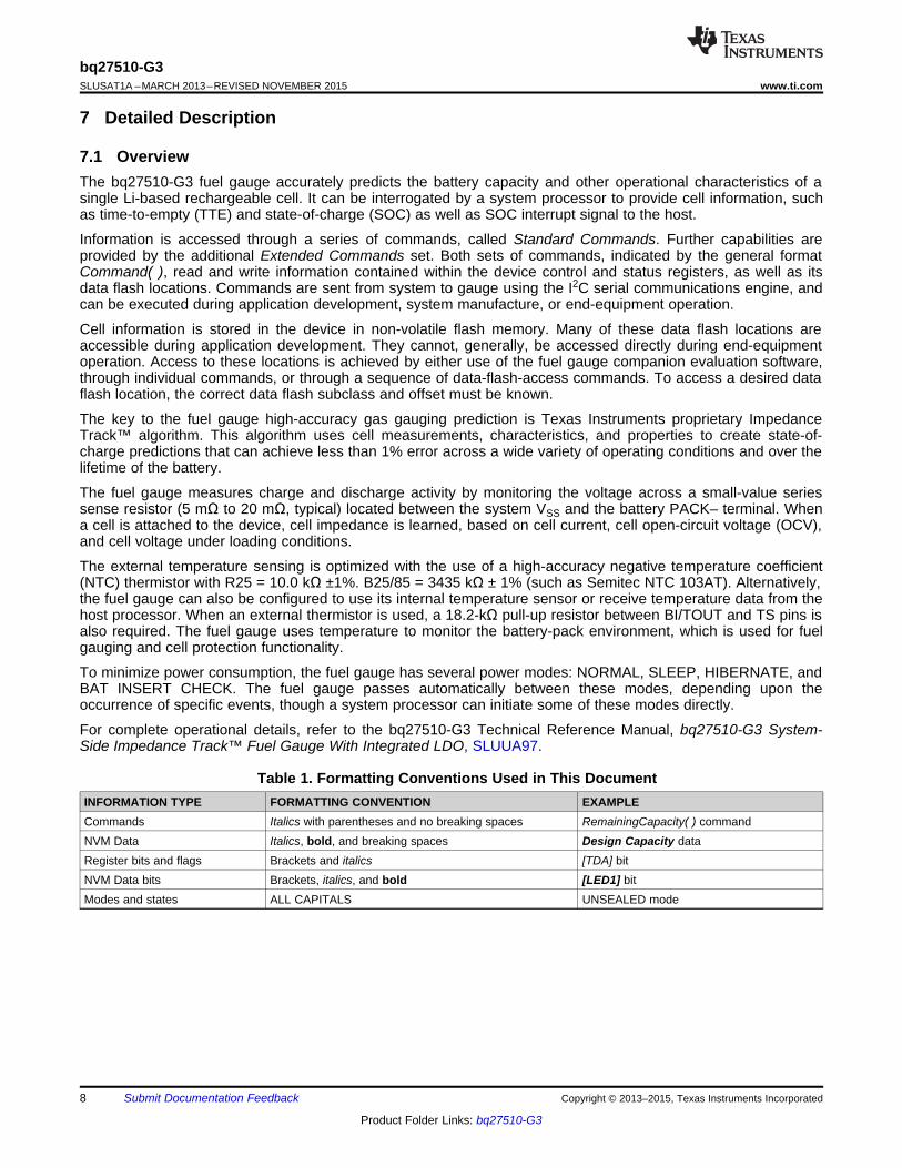
7.1 OverviewThe bq27510-G3 fuel gauge accurately predicts the battery capacity and other operational characteristics of asingle Li-based rechargeable cell. It can be interrogated by a system processor to provide cell information, suchas time-to-empty (TTE) and state-of-charge (SOC) as well as SOC interrupt signal to the host.
Information is accessed through a series of commands, called Standard Commands. Further capabilities areprovided by the additional Extended Commands set. Both sets of commands, indicated by the general formatCommand( ), read and write information contained within the device control and status registers, as well as itsdata flash locations. Commands are sent from system to gauge using the I2C serial communications engine, andcan be executed during application development, system manufacture, or end-equipment operation.
Cell information is stored in the device in non-volatile flash memory. Many of these data flash locations areaccessible during application development. They cannot, generally, be accessed directly during end-equipmentoperation. Access to these locations is achieved by either use of the fuel gauge companion evaluation software,through individual commands, or through a sequence of data-flash-access commands. To access a desired dataflash location, the correct data flash subclass and offset must be known.
The key to the fuel gauge high-accuracy gas gauging prediction is Texas Instruments proprietary ImpedanceTrack™ algorithm. This algorithm uses cell measurements, characteristics, and properties to create state-of-charge predictions that can achieve less than 1% error across a wide variety of operating conditions and over thelifetime of the battery.
The fuel gauge measures charge and discharge activity by monitoring the voltage across a small-value seriessense resistor (5 mΩ to 20 mΩ, typical) located between the system VSS and the battery PACK– terminal. Whena cell is attached to the device, cell impedance is learned, based on cell current, cell open-circuit voltage (OCV),and cell voltage under loading conditions.
The external temperature sensing is optimized with the use of a high-accuracy negative temperature coefficient(NTC) thermistor with R25 = 10.0 kΩ ±1%. B25/85 = 3435 kΩ ± 1% (such as Semitec NTC 103AT). Alternatively,the fuel gauge can also be configured to use its internal temperature sensor or receive temperature data from thehost processor. When an external thermistor is used, a 18.2-kΩ pull-up resistor between BI/TOUT and TS pins isalso required. The fuel gauge uses temperature to monitor the battery-pack environment, which is used for fuelgauging and cell protection functionality.
To minimize power consumption, the fuel gauge has several power modes: NORMAL, SLEEP, HIBERNATE, andBAT INSERT CHECK. The fuel gauge passes automatically between these modes, depending upon theoccurrence of specific events, though a system processor can initiate some of these modes directly.
For complete operational details, refer to the bq27510-G3 Technical Reference Manual, bq27510-G3 System-Side Impedance Track™ Fuel Gauge With Integrated LDO, SLUUA97.
Table 1. Formatting Conventions Used in This DocumentINFORMATION TYPE FORMATTING CONVENTION EXAMPLECommands Italics with parentheses and no breaking spaces RemainingCapacity( ) commandNVM Data Italics, bold, and breaking spaces Design Capacity dataRegister bits and flags Brackets and italics [TDA] bitNVM Data bits Brackets, italics, and bold [LED1] bitModes and states ALL CAPITALS UNSEALED mode
8 Submit Documentation Feedback Copyright © 2013–2015, Texas Instruments Incorporated
Product Folder Links: bq27510-G3

REGIN
BAT
VCC
TS
SRN
SRP
GPOUT SDA
VSS SCL
MUX
4R
Data FLASH
LDO
DataSRAM
CC
ADC
2.5 V
R
Internal Temp
Sensor
Wake Comparator
Instruction FLASH
Instruction ROM
I2C Slave Engine
CPU
22
22
8 8
HFO LFO
GP Timer and
PWM
I/O Controller
Wake and
Watchdog Timer
HFO
HFO/128
HFO/128
HFO/4
POR
BI/TOUT
REG25
bq27510-G3www.ti.com SLUSAT1A –MARCH 2013–REVISED NOVEMBER 2015
7.2 Functional Block Diagram
Copyright © 2013–2015, Texas Instruments Incorporated Submit Documentation Feedback 9
Product Folder Links: bq27510-G3

bq27510-G3SLUSAT1A –MARCH 2013–REVISED NOVEMBER 2015 www.ti.com
7.3 Feature DescriptionThe fuel gauge measures the cell voltage, temperature, and current to determine battery SOC. The fuel gaugemonitors charge and discharge activity by sensing the voltage across a small-value (5 mΩ to 20 mΩ typical)resistor between the SRP and SRN pins and in series with the cell. By integrating charge passing through thebattery, the battery’s SOC is adjusted during battery charge or discharge.
The total battery capacity is found by comparing states of charge before and after applying the load with theamount of charge passed. When an application load is applied, the impedance of the cell is measured bycomparing the OCV obtained from a predefined function for present SOC with the measured voltage under load.Measurements of OCV and charge integration determine chemical state of charge and chemical capacity(Qmax). The initial Qmax values are taken from a cell manufacturers' data sheet multiplied by the number ofparallel cells. It is also used for the value in Design Capacity. The fuel gauge acquires and updates thebatteryimpedance profile during normal battery usage. It uses this profile, along with SOC and the Qmax value,to determine FullChargeCapacity() and StateOfCharge(), specifically for the present load and temperature.FullChargeCapacity() is reported as capacity available from a fully charged battery under the present load andtemperature until Voltage() reaches the Terminate Voltage. NominalAvailableCapacity() andFullAvailableCapacity() are the uncompensated (no or light load) versions of RemainingCapacity() andFullChargeCapacity() respectively.
The fuel gauge has two flags accessed by the Flags() function that warns when the battery’s SOC has fallen tocritical levels. When StateOfCharge() falls below the first capacity threshold, specified in SOC1 Set Threshold,the [SOC1] (State of Charge Initial) flag is set. The flag is cleared once StateOfCharge() rises above SOC1 ClearThreshold. The fuel gauge’s GPOUT pin puts out 3 pulses 10ms wide and in 10ms intervals whenever theSOC1 flag is set. This flag is enabled when RMC_IND bit in Operation Configuration B is set. This behavioralso applies to the [SOCF] (State of Charge Final) flag.
When Voltage( ) falls below the system shut down threshold voltage, SysDown Set Volt Threshold, the[SYSDOWN] flag is set, serving as a final warning to shut down the system. The GPOUT also signals. WhenVoltage( ) rises above SysDown Clear Voltage and the [SYSDOWN] flag has already been set, the[SYSDOWN] flag is cleared. The GPOUT also signals such change. All units are in mV. Additional details arefound in the bq27510-G3 Technical Reference Manual, bq27510-G3 System-Side Impedance Track™ FuelGauge With Integrated LDO, SLUUA97.
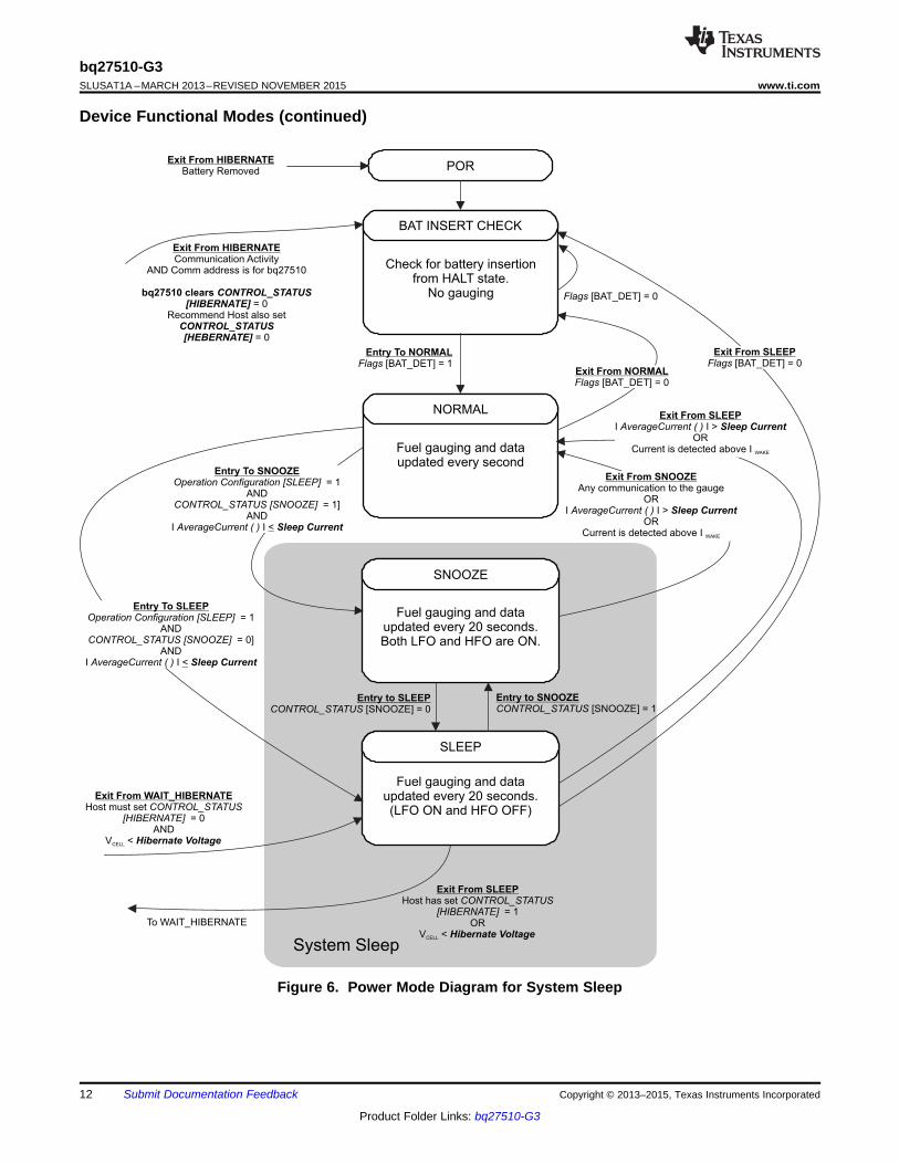
7.4 Device Functional Modes
7.4.1 Power ModesThe fuel gauge has different power modes: BAT INSERT CHECK, NORMAL, SNOOZE, SLEEP, andHIBERNATE. In NORMAL mode, the fuel gauge is fully powered and can execute any allowable task. InSNOOZE mode, both low-frequency and high-frequency oscillators are active. Although the SNOOZE mode hashigher current consumption than the SLEEP mode, it is also a reduced-power mode. In SLEEP mode, the fuelgauge turns off the high-frequency oscillator and exists in a reduced-power state, periodically takingmeasurements and performing calculations. In HIBERNATE mode, the fuel gauge is in a low-power state, butcan be woken up by communication or certain IO activity. Finally, the BAT INSERT CHECK mode is a poweredup, but low-power halted, state, where the fuel gauge resides when no battery is inserted into the system.
Figure 5 and Figure 6 show the relationship between these modes.
10 Submit Documentation Feedback Copyright © 2013–2015, Texas Instruments Incorporated
Product Folder Links: bq27510-G3

System Shutdown
HIBERNATE
Disable all bq27510subcircuits except GPIO
Negate BAT_GD
WAIT_HIBERNATE
Fuel gauging and dataupdated every 20 seconds.
unchanged.BAT_GD
Wakeup From HIBERNATECommunication Activity
ANDComm address is not for
bq27510
Exit From WAIT_HIBERNATECell relaxed
ANDAverageCurrent () <
ORCell relaxed
ANDV <
Ι Ι HibernateCurrent
Hibernate VoltageCELL
To SLEEP
POR
BAT INSERT CHECK
Check for battery insertionfrom HALT state.
No gauging
NORMAL
Fuel gauging and dataupdated every second.
Entry To NORMAL[BAT_DET] = 1Flags
Exit From WAIT_HIBERNATEHost must set
= 0AND
CONTROL_STATUS[HIBERNATE]
V <CELL Hibernate Voltage
Exit From SLEEPHost has set
= 1OR
CONTROL_STATUS[HIBERNATE]
V <CELL Hibernate Voltage
Flags [BAT_DET] = 0
Exit From NORMAL[BAT_DET] = 0Flags
Exit From SLEEP[BAT_DET] = 0Flags
Exit From HIBERNATEBattery Removed
Exit From HIBERNATECommunication Activity
AND Comm address is for bq27510
= 0Recommend Host also set
= 0
bq27510 clears CONTROL_STATUS[HIBERNATE]
CONTROL_STATUS[HEBERNATE]
bq27510-G3www.ti.com SLUSAT1A –MARCH 2013–REVISED NOVEMBER 2015
Device Functional Modes (continued)
Figure 5. Power Mode Diagram for System Shutdown
Copyright © 2013–2015, Texas Instruments Incorporated Submit Documentation Feedback 11
Product Folder Links: bq27510-G3
POR
BAT INSERT CHECK
Check for battery insertionfrom HALT state.
No gauging
System Sleep
SNOOZE
SLEEP
Fuel gauging and dataupdated every 20 seconds.Both LFO and HFO are ON.
Entry to SLEEP[SNOOZE] = 0CONTROL_STATUS
Exit From HIBERNATEBattery Removed
NORMAL
Fuel gauging and dataupdated every second
Exit From HIBERNATECommunication Activity
AND Comm address is for bq27510
= 0Recommend Host also set
= 0
bq27510 clears CONTROL_STATUS[HIBERNATE]
CONTROL_STATUS[HEBERNATE]
Entry To NORMAL[BAT_DET] = 1Flags
Flags [BAT_DET] = 0
Fuel gauging and dataupdated every 20 seconds.(LFO ON and HFO OFF)
Exit From SLEEPHost has set
= 1OR
CONTROL_STATUS[HIBERNATE]
V <CELL Hibernate Voltage
To WAIT_HIBERNATE
Entry to SNOOZE[SNOOZE] = 1CONTROL_STATUS
Exit From SLEEP>
ORCurrent is detected above
Ι Ι
Ι
AverageCurrent ( ) Sleep Current
WAKE
Exit From SNOOZEAny communication to the gauge
OR>
ORCurrent is detected above
Ι Ι
Ι
AverageCurrent ( ) Sleep Current
WAKE
Exit From NORMAL[BAT_DET] = 0Flags
Exit From WAIT_HIBERNATEHost must set
= 0AND
CONTROL_STATUS[HIBERNATE]
V <CELL Hibernate Voltage
Entry To SNOOZE= 1
AND= 1]
Operation Configuration [SLEEP]
CONTROL_STATUS [SNOOZE]AND
Ι ΙAverageCurrent ( ) < Sleep Current
Entry To SLEEP= 1
AND= 0]
Operation Configuration [SLEEP]
CONTROL_STATUS [SNOOZE]AND
Ι ΙAverageCurrent ( ) < Sleep Current
Exit From SLEEP[BAT_DET] = 0Flags
bq27510-G3SLUSAT1A –MARCH 2013–REVISED NOVEMBER 2015 www.ti.com
Device Functional Modes (continued)
Figure 6. Power Mode Diagram for System Sleep
12 Submit Documentation Feedback Copyright © 2013–2015, Texas Instruments Incorporated
Product Folder Links: bq27510-G3

bq27510-G3www.ti.com SLUSAT1A –MARCH 2013–REVISED NOVEMBER 2015
7.5 Programming
7.5.1 Standard Data CommandsThe bq27510-G3 fuel gauge uses a series of 2-byte standard commands to enable system reading and writing ofbattery information. Each standard command has an associated command-code pair, as indicated in Table 2.Because each command consists of two bytes of data, two consecutive I2C transmissions must be executed bothto initiate the command function, and to read or write the corresponding two bytes of data. Additional options fortransferring data are described in Communications. Standard commands are accessible in NORMAL operation.Read and write permissions depend on the active access mode, SEALED or UNSEALED. Additional details arefound in the bq27510-G3 Technical Reference Manual, SLUUA97.
Table 2. Standard CommandsNAME COMMAND CODE UNIT SEALED ACCESS
Control( ) 0x00 / 0x01 N/A R/WAtRate( ) 0x02 / 0x03 mA R/WAtRateTimeToEmpty( ) 0x04 / 0x05 minutes RTemperature( ) 0x06 / 0x07 0.1 K R/WVoltage( ) 0x08 / 0x09 mV RFlags( ) 0x0a / 0x0b N/A RNominalAvailableCapacity( ) 0x0c / 0x0d mAh RFullAvailableCapacity( ) 0x0e / 0x0f mAh RRemainingCapacity( ) 0x10 / 0x11 mAh RFullChargeCapacity( ) 0x12 / 0x13 mAh RAverageCurrent( ) 0x14 / 0x15 mA RTimeToEmpty( ) 0x16 / 0x17 minutes RStandbyCurrent( ) 0x18 / 0x19 mA RStandbyTimeToEmpty( ) 0x1a/ 0x1b minutes RStateOfHealth( ) 0x1c / 0x1d % / num RCycleCount( ) 0x1e/ 0x1f num RStateOfCharge( ) 0x20/ 0x21 % RnstantaneousCurrent( ) 0x22 / 0x23 mA RnternalTemperature( ) 0x28 / 0x29 0.1 K RResistanceScale( ) 0x2a / 0x2b ROperationConfiguration( ) 0x2c/ 0x2d N/A RDesignCapacity( ) 0x2e / 0x2f mAh R
Copyright © 2013–2015, Texas Instruments Incorporated Submit Documentation Feedback 13
Product Folder Links: bq27510-G3

Host generated
A AS 0ADDR[6:0] CMD[7:0] Sr 1ADDR[6:0] A DATA [7:0] A DATA [7:0] PN. . .
(d) incremental read
A AS 0ADDR[6:0] CMD[7:0] Sr 1ADDR[6:0] A DATA [7:0] PN
(c) 1- byte read
A AS A0 PADDR[6:0] CMD[7:0] DATA [7:0]
(a) 1-byte write (b) quick read
S 1ADDR[6:0] A DATA [7:0] PN
Gauge generated
. . .A AS A0 PADDR[6:0] CMD[7:0] DATA [7:0] DATA [7:0] A A
(e) incremental write
(S = Start , Sr = Repeated Start , A = Acknowledge , N = No Acknowledge , and P = Stop).
bq27510-G3SLUSAT1A –MARCH 2013–REVISED NOVEMBER 2015 www.ti.com
7.5.1.1 Control( ): 0x00/0x01Issuing a Control( ) command requires a subsequent 2-byte subcommand. These additional bytes specify theparticular control function desired. The Control( ) command allows the system to control specific features of thefuel gauge during normal operation and additional features when the device is in different access modes, asdescribed in Table 3. Additional details are found in the bq27510-G3 Technical Reference Manual, SLUUA97.
Table 3. Control( ) SubcommandsCNTL FUNCTION CNTL DATA SEALED ACCESS DESCRIPTION
CONTROL_STATUS 0x0000 Yes Reports the status of DF checksum, hibernate, IT, and so forthDEVICE_TYPE 0x0001 Yes Reports the device type (for example: 0x0520)FW_VERSION 0x0002 Yes Reports the firmware version on the device typePREV_MACWRITE 0x0007 Yes Returns previous Control( ) subcommand codeCHEM_ID 0x0008 Yes Reports the chemical identifier of the Impedance Track™ configurationOCV_CMD 0x000C Yes Requests the fuel gauge to take an OCV measurementBAT_INSERT 0x000D Yes Forces Flags( ) [BAT_DET] bit set when OpConfig B [BIE] = 0BAT_REMOVE 0x000E Yes Forces Flags( ) [BAT_DET] bit clear when OpConfig B [BIE] = 0SET_HIBERNATE 0x0011 Yes Forces CONTROL_STATUS [HIBERNATE] to 1CLEAR_HIBERNATE 0x0012 Yes Forces CONTROL_STATUS [HIBERNATE] to 0SET_SLEEP+ 0x0013 Yes Forces CONTROL_STATUS [SNOOZE] to 1CLEAR_SLEEP+ 0x0014 Yes Forces CONTROL_STATUS [SNOOZE] to 0DF_VERSION 0x001F Yes Returns the Data Flash Version codeSEALED 0x0020 No Places the fuel gauge in SEALED access modeIT_ENABLE 0x0021 No Enables the Impedance Track™ (IT) algorithmRESET 0x0041 No Forces a full reset of the fuel gauge
7.5.2 Communications
7.5.2.1 I2C InterfaceThe bq27510-G3 fuel gauge supports the standard I2C read, incremental read, quick read, one byte write, andincremental write functions. The 7-bit device address (ADDR) is the most significant 7 bits of the hex addressand is fixed as 1010101. The first 8-bits of the I2C protocol is, therefore, 0xAA or 0xAB for write or read,respectively.
Figure 7. I2C Read, Incremental Read, Quick Read, One Byte Write, and Incremental Write Functions
14 Submit Documentation Feedback Copyright © 2013–2015, Texas Instruments Incorporated
Product Folder Links: bq27510-G3
A AS 0ADDR [6:0] CMD [7:0] Sr 1ADDR [6:0] A DATA [7:0] A DATA [7:0] PN
A AS A0 PADDR [6:0] CMD [7:0] DATA [7:0] DATA [7:0] A 66 sm
A AS 0ADDR [6:0] CMD [7:0] Sr 1ADDR [6:0] A DATA [7:0] A DATA [7:0] A
DATA [7:0] A DATA [7:0] PN
Waiting time inserted between incremental 2-byte write packet for a subcommand and reading results
(acceptable for 100 kHz)fSCL £
Waiting time inserted after incremental read
66 sm
66 sm
A AS 0ADDR [6:0] CMD [7:0] Sr 1ADDR [6:0] A DATA [7:0] A DATA [7:0] PN
A AS A0 PADDR [6:0] CMD [7:0] DATA [7:0] 66 sm
Waiting time inserted between two 1-byte write packets for a subcommand and reading results
(required for 100 kHz < f 400 kHz)SCL £
66 sm
A AS A0 PADDR [6:0] CMD [7:0] DATA [7:0] 66 sm
bq27510-G3www.ti.com SLUSAT1A –MARCH 2013–REVISED NOVEMBER 2015
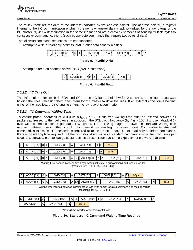
The “quick read” returns data at the address indicated by the address pointer. The address pointer, a registerinternal to the I2C communication engine, increments whenever data is acknowledged by the fuel gauge or theI2C master. “Quick writes” function in the same manner and are a convenient means of sending multiple bytes toconsecutive command locations (such as two-byte commands that require two bytes of data)
The following command sequences are not supported:Attempt to write a read-only address (NACK after data sent by master):
Figure 8. Invalid Write
Attempt to read an address above 0x6B (NACK command):
Figure 9. Invalid Read
7.5.2.2 I2C Time OutThe I2C engine releases both SDA and SCL if the I2C bus is held low for 2 seconds. If the fuel gauge washolding the lines, releasing them frees them for the master to drive the lines. If an external condition is holdingeither of the lines low, the I2C engine enters the low-power sleep mode.
7.5.2.3 I2C Command Waiting TimeTo ensure proper operation at 400 kHz, a t(BUF) ≥ 66 μs bus free waiting time must be inserted between allpackets addressed to the fuel gauge. In addition, if the SCL clock frequency (fSCL) is > 100 kHz, use individual 1-byte write commands for proper data flow control. The following diagram shows the standard waiting timerequired between issuing the control subcommand the reading the status result. For read-write standardcommand, a minimum of 2 seconds is required to get the result updated. For read-only standard commands,there is no waiting time required, but the host should not issue all standard commands more than two times persecond. Otherwise, the fuel gauge could result in a reset issue due to the expiration of the watchdog timer.
Figure 10. Standard I2C Command Waiting Time Required
Copyright © 2013–2015, Texas Instruments Incorporated Submit Documentation Feedback 15
Product Folder Links: bq27510-G3

bq27510-G3SLUSAT1A –MARCH 2013–REVISED NOVEMBER 2015 www.ti.com
7.5.2.4 I2C Clock StretchingA clock stretch can occur during all modes of fuel gauge operation. In SLEEP and HIBERNATE modes, a shortclock stretch occurs on all I2C traffic as the device must wake-up to process the packet. In the other modes (BATINSERT CHECK, NORMAL) clock stretching only occurs for packets addressed for the fuel gauge. The majorityof clock stretch periods are small as the I2C interface performs normal data flow control. However, less frequentyet more significant clock stretch periods may occur as blocks of Data Flash are updated. The following tablesummarizes the approximate clock stretch duration for various fuel gauge operating conditions.
Table 4. Approximate Clock Stretch DurationGAUGING APPROXIMATEOPERATING CONDITION OR COMMENTMODE DURATION
SLEEP Clock stretch occurs at the beginning of all traffic as the device wakes up. ≤ 4 msHIBERNATEBAT INSERT Clock stretch occurs within the packet for flow control (after a start bit, ACK or first data bit). ≤ 4 msCHECK, Normal Ra table Data Flash updates. 24 msNORMAL
Data Flash block writes. 72 msRestored Data Flash block write after loss of power. 116 msEnd of discharge Ra table Data Flash update. 144 ms
16 Submit Documentation Feedback Copyright © 2013–2015, Texas Instruments Incorporated
Product Folder Links: bq27510-G3

bq27510DRZGPOUT
GPOUT
bq27510-G3www.ti.com SLUSAT1A –MARCH 2013–REVISED NOVEMBER 2015
8 Application and Implementation
NOTEInformation in the following applications sections is not part of the TI componentspecification, and TI does not warrant its accuracy or completeness. TI’s customers areresponsible for determining suitability of components for their purposes. Customers shouldvalidate and test their design implementation to confirm system functionality.
8.1 Application InformationThe bq27510-G3 system-side Li-Ion battery fuel gauge is a microcontroller peripheral that provides fuel gaugingfor single-cell Li-Ion battery packs. The device requires little system microcontroller firmware development. Thefuel resides on the main board of the system and manages an embedded battery (non-removable) or a up to32000-mAhr Capacity removable battery pack.To allow for optimal performance in the end application, specialconsiderations must be taken to ensure minimization of measurement error through proper printed circuit board(PCB) board layout. Such requirements are detailed in Design Requirements.
8.2 Typical Application
Figure 11. bq27510-G3 Typical Application
8.2.1 Design RequirementsSeveral key parameters must be updated to align with a given application's battery characteristics. For highestaccuracy gauging, it is important to follow-up this initial configuration with a learning cycle to optimize resistanceand maximum chemical capacity (Qmax) values prior to sealing and shipping systems to the field. Successfuland accurate configuration of the fuel gauge for a target application can be used as the basis for creating a"golden" gas gauge (.fs) file that can be written to all gauges, assuming identical pack design and Li-ion cellorigin (chemistry, lot, and so on). Calibration data is included as part of this golden GG file to cut down onsystem production time. If going this route, it is recommended to average the voltage and current measurementcalibration data from a large sample size and use these in the golden file. Table 5, Key Data Flash Parametersfor Configuration, shows the items that should be configured to achieve reliable protection and accurate gaugingwith minimal initial configuration.
Copyright © 2013–2015, Texas Instruments Incorporated Submit Documentation Feedback 17
Product Folder Links: bq27510-G3

bq27510-G3SLUSAT1A –MARCH 2013–REVISED NOVEMBER 2015 www.ti.com
Typical Application (continued)Table 5. Key Data Flash Parameters for Configuration
NAME DEFAULT UNIT RECOMMENDED SETTINGSet based on the nominal pack capacity as interpreted from cell manufacturer'sDesign Capacity 1000 mAh datasheet. If multiple parallel cells are used, should be set to N × Cell Capacity.Set to 10 to convert all power values to cWh or to 1 for mWh. Design EnergyDesign Energy Scale 1 - is divided by this value.Set to desired runtime remaining (in seconds / 3600) × typical applied loadReserve Capacity-mAh 0 mAh between reporting 0% SOC and reaching Terminate Voltage, if needed.Should be configured using TI-supplied Battery Management Studio software.Default open-circuit voltage and resistance tables are also updated in
Chem ID 0100 hex conjunction with this step. Do not attempt to manually update reported DeviceChemistry as this does not change all chemistry information! Always updatechemistry using the appropriate software tool (that is, bqStudio).
Load Mode 1 - Set to applicable load model, 0 for constant current or 1 for constant power.Load Select 1 - Set to load profile which most closely matches typical system load.
Set to initial configured value for Design Capacity. The gauge will update thisQmax Cell 0 1000 mAh parameter automatically after the optimization cycle and for every regular
Qmax update thereafter.Set to nominal cell voltage for a fully charged cell. The gauge will update thisCell0 V at Chg Term 4200 mV parameter automatically each time full charge termination is detected.Set to empty point reference of battery based on system needs. Typical isTerminate Voltage 3200 mV between 3000 and 3200 mV.
Ra Max Delta 44 mΩ Set to 15% of Cell0 R_a 4 resistance after an optimization cycle is completed.Set based on nominal charge voltage for the battery in normal conditions
Charging Voltage 4200 mV (25°C, etc). Used as the reference point for offsetting by Taper Voltage for fullcharge termination detection.Set to the nominal taper current of the charger + taper current tolerance toTaper Current 100 mA ensure that the gauge will reliably detect charge termination.Sets the voltage window for qualifying full charge termination. Can be set
Taper Voltage 100 mV tighter to avoid or wider to ensure possibility of reporting 100% SOC in outerJEITA temperature ranges that use derated charging voltage.Sets threshold for gauge detecting battery discharge. Should be set lower thanDsg Current Threshold 60 mA minimal system load expected in the application and higher than Quit Current.Sets the threshold for detecting battery charge. Can be set higher or lower
Chg Current Threshold 75 mA depending on typical trickle charge current used. Also should be set higherthan Quit Current.Sets threshold for gauge detecting battery relaxation. Can be set higher orQuit Current 40 mA lower depending on typical standby current and exhibited in the end system.Current profile used in capacity simulations at onset of discharge or at all times
Avg I Last Run –299 mA if Load Select = 0. Should be set to nominal system load. Is automaticallyupdated by the gauge every cycle.Power profile used in capacity simulations at onset of discharge or at all times
Avg P Last Run –1131 mW if Load Select = 0. Should be set to nominal system power. Is automaticallyupdated by the gauge every cycle.Sets the threshold at which the fuel gauge enters SLEEP mode. Take care in
Sleep Current 10 mA setting above typical standby currents else entry to SLEEP may beunintentionally blocked.Calibrate this parameter using TI-supplied bqStudio software and calibration
CC Gain 10 mohms procedure in the TRM. Determines conversion of coulomb counter measuredsense resistor voltage to current.Calibrate this parameter using TI-supplied bqStudio software and calibration
CC Delta 10 mohms procedure in the TRM. Determines conversion of coulomb counter measuredsense resistor voltage to passed charge.Calibrate this parameter using TI-supplied bqStudio software and calibration
Board Offset 0 Counts procedure in the TRM. Determines native offset of the printed circuit boardparasitics that should be removed from conversions.
18 Submit Documentation Feedback Copyright © 2013–2015, Texas Instruments Incorporated
Product Folder Links: bq27510-G3

bq27510-G3www.ti.com SLUSAT1A –MARCH 2013–REVISED NOVEMBER 2015
Typical Application (continued)Table 5. Key Data Flash Parameters for Configuration (continued)
NAME DEFAULT UNIT RECOMMENDED SETTINGCalibrate this parameter using TI-supplied bqStudio software and calibrationprocedure in the TRM. Determines voltage offset between cell tab and ADCPack V Offset 0 mV input node to incorporate back into or remove from measurement, dependingon polarity.
8.2.2 Detailed Design Procedure
8.2.2.1 BAT Voltage Sense InputA ceramic capacitor at the input to the BAT pin is used to bypass AC voltage ripple to ground, greatly reducingits influence on battery voltage measurements. It proves most effective in applications with load profiles thatexhibit high-frequency current pulses (that is, cell phones) but is recommended for use in all applications toreduce noise on this sensitive high-impedance measurement node.
8.2.2.2 SRP and SRN Current Sense InputsThe filter network at the input to the coulomb counter is intended to improve differential mode rejection of voltagemeasured across the sense resistor. These components should be placed as close as possible to the coulombcounter inputs and the routing of the differential traces length-matched to best minimize impedance mismatch-induced measurement errors.
8.2.2.3 Sense Resistor SelectionAny variation encountered in the resistance present between the SRP and SRN pins of the fuel gauge will affectthe resulting differential voltage, and derived current, it senses. As such, it is recommended to select a senseresistor with minimal tolerance and temperature coefficient of resistance (TCR) characteristics. The standardrecommendation based on best compromise between performance and price is a 1% tolerance, 100 ppm driftsense resistor with a 1-W power rating.
8.2.2.4 TS Temperature Sense InputSimilar to the BAT pin, a ceramic decoupling capacitor for the TS pin is used to bypass AC voltage ripple awayfrom the high-impedance ADC input, minimizing measurement error. Another helpful advantage is that thecapacitor provides additional ESD protection since the TS input to system may be accessible in systems that useremovable battery packs. It should be placed as close as possible to the respective input pin for optimal filteringperformance.
8.2.2.5 Thermistor SelectionThe fuel gauge temperature sensing circuitry is designed to work with a negative temperature coefficient-type(NTC) thermistor with a characteristic 10-kΩ resistance at room temperature (25°C). The default curve-fittingcoefficients configured in the fuel gauge specifically assume a 103AT-2 type thermistor profile and so that is thedefault recommendation for thermistor selection purposes. Moving to a separate thermistor resistance profile (forexample, JT-2 or others) requires an update to the default thermistor coefficients in data flash to ensure highestaccuracy temperature measurement performance.
8.2.2.6 REGIN Power Supply Input FilteringA ceramic capacitor is placed at the input to the fuel gauge internal LDO to increase power supply rejection(PSR) and improve effective line regulation. It ensures that voltage ripple is rejected to ground instead ofcoupling into the internal supply rails of the fuel gauge.
8.2.2.7 VCC LDO Output FilteringA ceramic capacitor is also needed at the output of the internal LDO to provide a current reservoir for fuel gaugeload peaks during high peripheral utilization. It acts to stabilize the regulator output and reduce core voltageripple inside of the fuel gauge.
Copyright © 2013–2015, Texas Instruments Incorporated Submit Documentation Feedback 19
Product Folder Links: bq27510-G3

Temperature (qC)
HF
O (
MH
Z)
-40 -20 0 20 40 60 80 1008.365
8.37
8.375
8.38
8.385
8.39
8.395
8.4
D003
Temperature (qC)
RE
G2
5 O
utp
ut
(V)
-40 -20 0 20 40 60 80 1002.44
2.46
2.48
2.5
2.52
2.54
2.56
2.58
D001
IOUT = 16 mA, REGIN = 5 VIOUT = 3 mA, REGIN = 2.7 V
Temperature (qC)
LF
O (
kH
Z)
-40 -20 0 20 40 60 80 10032.45
32.5
32.55
32.6
32.65
32.7
32.75
32.8
D002
bq27510-G3SLUSAT1A –MARCH 2013–REVISED NOVEMBER 2015 www.ti.com
8.2.3 Application Curves
Figure 12. REG25 vs. Temperature Figure 13. Low Frequency Oscillator vs. Temperature
Figure 14. High Frequency Oscillator vs. Temperature
9 Power Supply Recommendations
9.1 Power Supply DecouplingBoth the REGIN input pin and the VCC output pin require low equivalent series resistance (ESR) ceramiccapacitors placed as closely as possible to the respective pins to optimize ripple rejection and provide a stableand dependable power rail that is resilient to line transients. A 0.1-µF capacitor at the REGIN and a 1-µFcapacitor at VCC will suffice for satisfactory device performance.
20 Submit Documentation Feedback Copyright © 2013–2015, Texas Instruments Incorporated
Product Folder Links: bq27510-G3

CVCC
Use copper
pours for battery
power path to
minimize IR
losses
Place capacitors
close to gauge
IC. Trace to pin
and VSS should
be short
Via connects to Power Ground
Kelvin connect
BAT sense line
right at positive
battery terminal
Kelvin connect SRP
and SRN
connections right at
Rsense terminals
RESD3
RESD5
RESD4
RESD4
Use short and wide
traces to minimize
inductance
SCL
SDA
Star ground right at PACK-
for ESD return path
BI/
TOUT
REG25
REGIN
BAT
VCC
VSS
GPOUT
SCL
SDA
TS
SRN
SRP
CBAT
CREGIN
GPOUT
10m1%
PACKP
PACKN
Battery power
Connection to
System
THERM
BI/TOUT
Ground
Return to
system
R1
R2
bq27510-G3www.ti.com SLUSAT1A –MARCH 2013–REVISED NOVEMBER 2015
10 Layout
10.1 Layout Guidelines
10.1.1 Sense Resistor ConnectionsKelvin connections at the sense resistor are just as critical as those for the battery terminals themselves. Thedifferential traces should be connected at the inside of the sense resistor pads and not anywhere along the high-current trace path to prevent false increases to measured current that could result when measuring between thesum of the sense resistor and trace resistance between the tap points. In addition, the routing of these leadsfrom the sense resistor to the input filter network and finally into the SRP and SRN pins needs to be as closelymatched in length as possible else additional measurement offset could occur. It is further recommended to addcopper trace or pour-based "guard rings" around the perimeter of the filter network and coulomb counter inputs toshield these sensitive pins from radiated EMI into the sense nodes. This prevents differential voltage shifts thatcould be interpreted as real current change to the fuel gauge. All of the filter components need to be placed asclose as possible to the coulomb counter input pins.
10.1.2 Thermistor ConnectionsThe thermistor sense input should include a ceramic bypass capacitor placed as close to the TS input pin aspossible. The capacitor helps to filter measurements of any stray transients as the voltage bias circuit pulsesperiodically during temperature sensing windows.
10.1.3 High-Current and Low-Current Path SeparationFor best possible noise performance, it is extremely important to separate the low-current and high-current loopsto different areas of the board layout. The fuel gauge and all support components should be situated on one sideof the boards and tap off of the high-current loop (for measurement purposes) at the sense resistor. Routing thelow-current ground around instead of under high-current traces will further help to improve noise rejection.
10.2 Layout Example
Figure 15. bq27510-G3 Board Layout
Copyright © 2013–2015, Texas Instruments Incorporated Submit Documentation Feedback 21
Product Folder Links: bq27510-G3

bq27510-G3SLUSAT1A –MARCH 2013–REVISED NOVEMBER 2015 www.ti.com
11 Device and Documentation Support
11.1 Device Support
11.1.1 Third-Party Products DisclaimerTI'S PUBLICATION OF INFORMATION REGARDING THIRD-PARTY PRODUCTS OR SERVICES DOES NOTCONSTITUTE AN ENDORSEMENT REGARDING THE SUITABILITY OF SUCH PRODUCTS OR SERVICESOR A WARRANTY, REPRESENTATION OR ENDORSEMENT OF SUCH PRODUCTS OR SERVICES, EITHERALONE OR IN COMBINATION WITH ANY TI PRODUCT OR SERVICE.
11.2 Documentation Support
11.2.1 Related DocumentationFor related documentation see the following:• bq27510-G3 Technical Reference Manual, bq27510-G3 System-Side Impedance Track™ Fuel Gauge With
Integrated LDO, SLUUA97
11.3 Community ResourcesThe following links connect to TI community resources. Linked contents are provided "AS IS" by the respectivecontributors. They do not constitute TI specifications and do not necessarily reflect TI's views; see TI's Terms ofUse.
TI E2E™ Online Community TI's Engineer-to-Engineer (E2E) Community. Created to foster collaborationamong engineers. At e2e.ti.com, you can ask questions, share knowledge, explore ideas and helpsolve problems with fellow engineers.
Design Support TI's Design Support Quickly find helpful E2E forums along with design support tools andcontact information for technical support.
11.4 TrademarksImpedance Track, E2E are trademarks of Texas Instruments.All other trademarks are the property of their respective owners.
11.5 Electrostatic Discharge CautionThese devices have limited built-in ESD protection. The leads should be shorted together or the device placed in conductive foamduring storage or handling to prevent electrostatic damage to the MOS gates.
11.6 GlossarySLYZ022 — TI Glossary.
This glossary lists and explains terms, acronyms, and definitions.
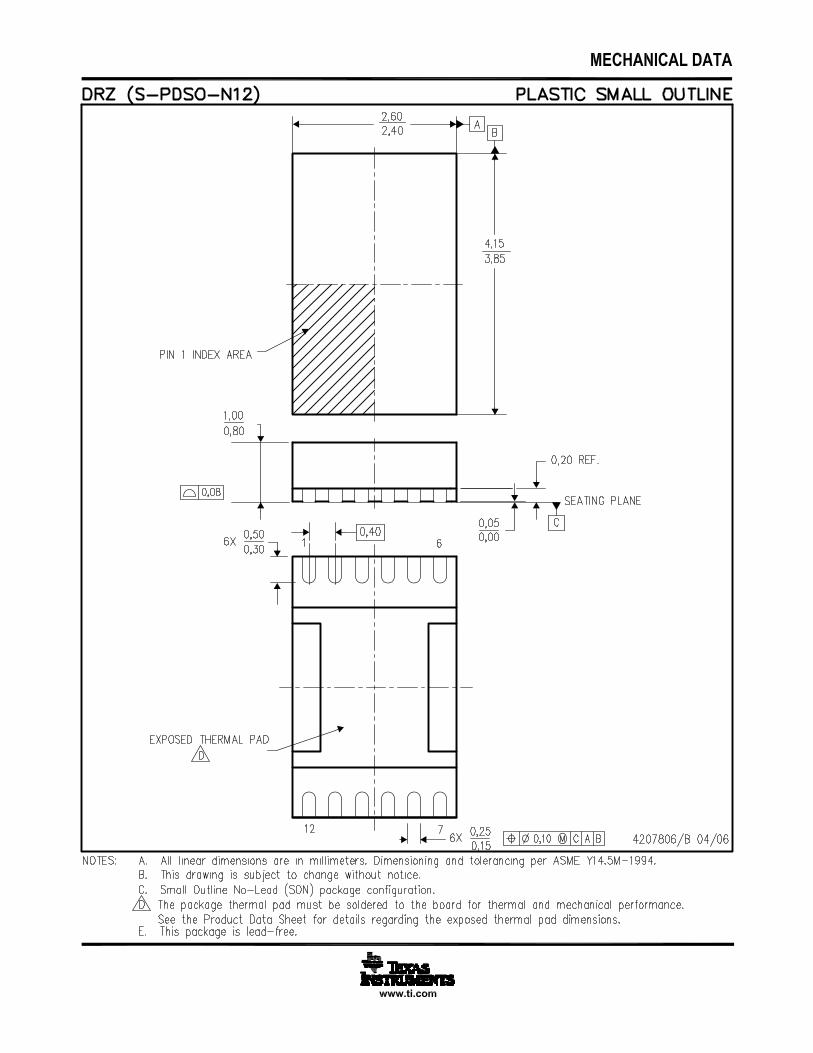
12 Mechanical, Packaging, and Orderable InformationThe following pages include mechanical, packaging, and orderable information. This information is the mostcurrent data available for the designated devices. This data is subject to change without notice and revision ofthis document. For browser-based versions of this data sheet, refer to the left-hand navigation.
22 Submit Documentation Feedback Copyright © 2013–2015, Texas Instruments Incorporated
Product Folder Links: bq27510-G3

PACKAGE OPTION ADDENDUM
www.ti.com 29-Oct-2015
Addendum-Page 1
PACKAGING INFORMATION
Orderable Device Status(1)
Package Type PackageDrawing
Pins PackageQty
Eco Plan(2)
Lead/Ball Finish(6)
MSL Peak Temp(3)
Op Temp (°C) Device Marking(4/5)
Samples
BQ27510DRZR-G3 ACTIVE SON DRZ 12 3000 Green (RoHS& no Sb/Br)
CU NIPDAU Level-2-260C-1 YEAR -40 to 85 BQ7510
BQ27510DRZT-G3 ACTIVE SON DRZ 12 250 Green (RoHS& no Sb/Br)
CU NIPDAU Level-2-260C-1 YEAR -40 to 85 BQ7510
(1) The marketing status values are defined as follows:ACTIVE: Product device recommended for new designs.LIFEBUY: TI has announced that the device will be discontinued, and a lifetime-buy period is in effect.NRND: Not recommended for new designs. Device is in production to support existing customers, but TI does not recommend using this part in a new design.PREVIEW: Device has been announced but is not in production. Samples may or may not be available.OBSOLETE: TI has discontinued the production of the device.
(2) Eco Plan - The planned eco-friendly classification: Pb-Free (RoHS), Pb-Free (RoHS Exempt), or Green (RoHS & no Sb/Br) - please check http://www.ti.com/productcontent for the latest availabilityinformation and additional product content details.TBD: The Pb-Free/Green conversion plan has not been defined.Pb-Free (RoHS): TI's terms "Lead-Free" or "Pb-Free" mean semiconductor products that are compatible with the current RoHS requirements for all 6 substances, including the requirement thatlead not exceed 0.1% by weight in homogeneous materials. Where designed to be soldered at high temperatures, TI Pb-Free products are suitable for use in specified lead-free processes.Pb-Free (RoHS Exempt): This component has a RoHS exemption for either 1) lead-based flip-chip solder bumps used between the die and package, or 2) lead-based die adhesive used betweenthe die and leadframe. The component is otherwise considered Pb-Free (RoHS compatible) as defined above.Green (RoHS & no Sb/Br): TI defines "Green" to mean Pb-Free (RoHS compatible), and free of Bromine (Br) and Antimony (Sb) based flame retardants (Br or Sb do not exceed 0.1% by weightin homogeneous material)
(3) MSL, Peak Temp. - The Moisture Sensitivity Level rating according to the JEDEC industry standard classifications, and peak solder temperature.
(4) There may be additional marking, which relates to the logo, the lot trace code information, or the environmental category on the device.
(5) Multiple Device Markings will be inside parentheses. Only one Device Marking contained in parentheses and separated by a "~" will appear on a device. If a line is indented then it is a continuationof the previous line and the two combined represent the entire Device Marking for that device.
(6) Lead/Ball Finish - Orderable Devices may have multiple material finish options. Finish options are separated by a vertical ruled line. Lead/Ball Finish values may wrap to two lines if the finishvalue exceeds the maximum column width.
Important Information and Disclaimer:The information provided on this page represents TI's knowledge and belief as of the date that it is provided. TI bases its knowledge and belief on informationprovided by third parties, and makes no representation or warranty as to the accuracy of such information. Efforts are underway to better integrate information from third parties. TI has taken andcontinues to take reasonable steps to provide representative and accurate information but may not have conducted destructive testing or chemical analysis on incoming materials and chemicals.TI and TI suppliers consider certain information to be proprietary, and thus CAS numbers and other limited information may not be available for release.
PACKAGE OPTION ADDENDUM
www.ti.com 29-Oct-2015
Addendum-Page 2
In no event shall TI's liability arising out of such information exceed the total purchase price of the TI part(s) at issue in this document sold by TI to Customer on an annual basis.
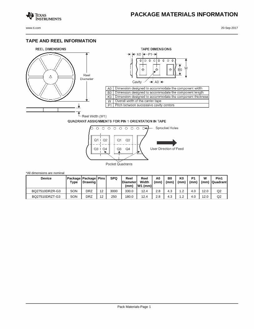
TAPE AND REEL INFORMATION
*All dimensions are nominal
Device PackageType
PackageDrawing
Pins SPQ ReelDiameter
(mm)
ReelWidth
W1 (mm)
A0(mm)
B0(mm)
K0(mm)
P1(mm)
W(mm)
Pin1Quadrant
BQ27510DRZR-G3 SON DRZ 12 3000 330.0 12.4 2.8 4.3 1.2 4.0 12.0 Q2
BQ27510DRZT-G3 SON DRZ 12 250 180.0 12.4 2.8 4.3 1.2 4.0 12.0 Q2
PACKAGE MATERIALS INFORMATION
www.ti.com 20-Sep-2017
Pack Materials-Page 1

*All dimensions are nominal
Device Package Type Package Drawing Pins SPQ Length (mm) Width (mm) Height (mm)
BQ27510DRZR-G3 SON DRZ 12 3000 367.0 367.0 35.0
BQ27510DRZT-G3 SON DRZ 12 250 210.0 185.0 35.0
PACKAGE MATERIALS INFORMATION
www.ti.com 20-Sep-2017
Pack Materials-Page 2


IMPORTANT NOTICE
Texas Instruments Incorporated (TI) reserves the right to make corrections, enhancements, improvements and other changes to itssemiconductor products and services per JESD46, latest issue, and to discontinue any product or service per JESD48, latest issue. Buyersshould obtain the latest relevant information before placing orders and should verify that such information is current and complete.TI’s published terms of sale for semiconductor products (http://www.ti.com/sc/docs/stdterms.htm) apply to the sale of packaged integratedcircuit products that TI has qualified and released to market. Additional terms may apply to the use or sale of other types of TI products andservices.Reproduction of significant portions of TI information in TI data sheets is permissible only if reproduction is without alteration and isaccompanied by all associated warranties, conditions, limitations, and notices. TI is not responsible or liable for such reproduceddocumentation. Information of third parties may be subject to additional restrictions. Resale of TI products or services with statementsdifferent from or beyond the parameters stated by TI for that product or service voids all express and any implied warranties for theassociated TI product or service and is an unfair and deceptive business practice. TI is not responsible or liable for any such statements.Buyers and others who are developing systems that incorporate TI products (collectively, “Designers”) understand and agree that Designersremain responsible for using their independent analysis, evaluation and judgment in designing their applications and that Designers havefull and exclusive responsibility to assure the safety of Designers' applications and compliance of their applications (and of all TI productsused in or for Designers’ applications) with all applicable regulations, laws and other applicable requirements. Designer represents that, withrespect to their applications, Designer has all the necessary expertise to create and implement safeguards that (1) anticipate dangerousconsequences of failures, (2) monitor failures and their consequences, and (3) lessen the likelihood of failures that might cause harm andtake appropriate actions. Designer agrees that prior to using or distributing any applications that include TI products, Designer willthoroughly test such applications and the functionality of such TI products as used in such applications.TI’s provision of technical, application or other design advice, quality characterization, reliability data or other services or information,including, but not limited to, reference designs and materials relating to evaluation modules, (collectively, “TI Resources”) are intended toassist designers who are developing applications that incorporate TI products; by downloading, accessing or using TI Resources in anyway, Designer (individually or, if Designer is acting on behalf of a company, Designer’s company) agrees to use any particular TI Resourcesolely for this purpose and subject to the terms of this Notice.TI’s provision of TI Resources does not expand or otherwise alter TI’s applicable published warranties or warranty disclaimers for TIproducts, and no additional obligations or liabilities arise from TI providing such TI Resources. TI reserves the right to make corrections,enhancements, improvements and other changes to its TI Resources. TI has not conducted any testing other than that specificallydescribed in the published documentation for a particular TI Resource.Designer is authorized to use, copy and modify any individual TI Resource only in connection with the development of applications thatinclude the TI product(s) identified in such TI Resource. NO OTHER LICENSE, EXPRESS OR IMPLIED, BY ESTOPPEL OR OTHERWISETO ANY OTHER TI INTELLECTUAL PROPERTY RIGHT, AND NO LICENSE TO ANY TECHNOLOGY OR INTELLECTUAL PROPERTYRIGHT OF TI OR ANY THIRD PARTY IS GRANTED HEREIN, including but not limited to any patent right, copyright, mask work right, orother intellectual property right relating to any combination, machine, or process in which TI products or services are used. Informationregarding or referencing third-party products or services does not constitute a license to use such products or services, or a warranty orendorsement thereof. Use of TI Resources may require a license from a third party under the patents or other intellectual property of thethird party, or a license from TI under the patents or other intellectual property of TI.TI RESOURCES ARE PROVIDED “AS IS” AND WITH ALL FAULTS. TI DISCLAIMS ALL OTHER WARRANTIES ORREPRESENTATIONS, EXPRESS OR IMPLIED, REGARDING RESOURCES OR USE THEREOF, INCLUDING BUT NOT LIMITED TOACCURACY OR COMPLETENESS, TITLE, ANY EPIDEMIC FAILURE WARRANTY AND ANY IMPLIED WARRANTIES OFMERCHANTABILITY, FITNESS FOR A PARTICULAR PURPOSE, AND NON-INFRINGEMENT OF ANY THIRD PARTY INTELLECTUALPROPERTY RIGHTS. TI SHALL NOT BE LIABLE FOR AND SHALL NOT DEFEND OR INDEMNIFY DESIGNER AGAINST ANY CLAIM,INCLUDING BUT NOT LIMITED TO ANY INFRINGEMENT CLAIM THAT RELATES TO OR IS BASED ON ANY COMBINATION OFPRODUCTS EVEN IF DESCRIBED IN TI RESOURCES OR OTHERWISE. IN NO EVENT SHALL TI BE LIABLE FOR ANY ACTUAL,DIRECT, SPECIAL, COLLATERAL, INDIRECT, PUNITIVE, INCIDENTAL, CONSEQUENTIAL OR EXEMPLARY DAMAGES INCONNECTION WITH OR ARISING OUT OF TI RESOURCES OR USE THEREOF, AND REGARDLESS OF WHETHER TI HAS BEENADVISED OF THE POSSIBILITY OF SUCH DAMAGES.Unless TI has explicitly designated an individual product as meeting the requirements of a particular industry standard (e.g., ISO/TS 16949and ISO 26262), TI is not responsible for any failure to meet such industry standard requirements.Where TI specifically promotes products as facilitating functional safety or as compliant with industry functional safety standards, suchproducts are intended to help enable customers to design and create their own applications that meet applicable functional safety standardsand requirements. Using products in an application does not by itself establish any safety features in the application. Designers mustensure compliance with safety-related requirements and standards applicable to their applications. Designer may not use any TI products inlife-critical medical equipment unless authorized officers of the parties have executed a special contract specifically governing such use.Life-critical medical equipment is medical equipment where failure of such equipment would cause serious bodily injury or death (e.g., lifesupport, pacemakers, defibrillators, heart pumps, neurostimulators, and implantables). Such equipment includes, without limitation, allmedical devices identified by the U.S. Food and Drug Administration as Class III devices and equivalent classifications outside the U.S.TI may expressly designate certain products as completing a particular qualification (e.g., Q100, Military Grade, or Enhanced Product).Designers agree that it has the necessary expertise to select the product with the appropriate qualification designation for their applicationsand that proper product selection is at Designers’ own risk. Designers are solely responsible for compliance with all legal and regulatoryrequirements in connection with such selection.Designer will fully indemnify TI and its representatives against any damages, costs, losses, and/or liabilities arising out of Designer’s non-compliance with the terms and provisions of this Notice.
Mailing Address: Texas Instruments, Post Office Box 655303, Dallas, Texas 75265Copyright © 2017, Texas Instruments Incorporated