bq24640 high-efficiency synchronous switched-mode super ... · pdf file1• charge super...
TRANSCRIPT

bq24
640 Super
Cap
HIDRV
LODRV
PH
SRNSRP
VFB
CE
VREF
ISET
ADAPTER
ADAPTERSTAT
PG
VREF
TS
Product
Folder
Sample &Buy
Technical
Documents
Tools &
Software
Support &Community
ReferenceDesign
bq24640SLUSA44A –MARCH 2010–REVISED JULY 2015
bq24640 High-Efficiency Synchronous Switched-Mode Super Capacitor Charger1 Features 2 Applications1• Charge Super Capacitor Pack From 2.1 V to 26 V • Memory Backup Systems• CC/CV Charge Profile From 0 V Without • Industrial UPS Systems and Power Transient
Precharge Buffering• 600-kHz NMOS-NMOS Synchronous Buck • Bridge Power to Buffer the Battery
Controller3 Description• Over 90% Efficiency for up to 10-A ChargeThe bq24640 device is a highly integrated switched-Currentmode super capacitor charge controller. The device• 5-V to 28-V VCC Input Voltage Rangeoffers a constant-frequency synchronous PWM
• Accuracy controller with high accuracy charge current, voltage– ±0.5% Charge Voltage Regulation regulation, and charge status monitoring.– ±3% Charge Current Regulation The bq24640 charges a super capacitor in two
phases: constant current and constant voltage• High Integration(CC/CV). The device can charge super capacitors– Internal Loop Compensationfrom 0 V with current set on the ISET pin. When the
– Internal Digital Soft Start super capacitor voltage reaches the programmed• Safety target voltage, charge current begins tapering down.
– Input Overvoltage Protection The bq24640 enters a low-current sleep mode(<15 μA) when the input voltage falls below the– Capacitor Temperature Sensing Hot and Coldoutput capacitor voltage.Charge Suspend
– Thermal Shutdown The bq24640 has an input CE pin to enable anddisable charge, and the STAT and PG output pins• Status Outputsreport charge and adapter status. The TS pin on the– Adapter Present bq24640 monitors the temperature of the capacitor
– Charger Operation Status and suspends charge during hot and cold conditions.• Charge Enable Pin
Device Information(1)• 30-ns Driver Dead Time and 99.5% Maximum
PART NUMBER PACKAGE BODY SIZE (NOM)Effective Duty Cyclebq24640 VQFN (16) 3.50 mm × 3.50 mm• Automatic Sleep Mode for Low Power(1) For all available packages, see the orderable addendum atConsumption
the end of the data sheet.– <15-µA Off-State Super Capacitor DischargeCurrent
– <1.5-mA Off-State Input Quiescent Current
Simplified Schematic
1
An IMPORTANT NOTICE at the end of this data sheet addresses availability, warranty, changes, use in safety-critical applications,intellectual property matters and other important disclaimers. PRODUCTION DATA.

bq24640SLUSA44A –MARCH 2010–REVISED JULY 2015 www.ti.com
Table of Contents7.4 Device Functional Modes........................................ 161 Features .................................................................. 1
8 Application and Implementation ........................ 172 Applications ........................................................... 18.1 Application Information............................................ 173 Description ............................................................. 18.2 Typical Application .................................................. 174 Revision History..................................................... 2
9 Power Supply Recommendations ...................... 215 Pin Configuration and Functions ......................... 310 Layout................................................................... 216 Specifications......................................................... 4
10.1 Layout Guidelines ................................................. 216.1 Absolute Maximum Ratings ..................................... 410.2 Layout Examples................................................... 226.2 ESD Ratings.............................................................. 4
11 Device and Documentation Support ................. 236.3 Recommended Operating Conditions....................... 511.1 Device Support...................................................... 236.4 Thermal Information .................................................. 511.2 Documentation Support ........................................ 236.5 Electrical Characteristics........................................... 511.3 Community Resources.......................................... 236.6 Typical Characteristics .............................................. 811.4 Trademarks ........................................................... 237 Detailed Description ............................................ 1011.5 Electrostatic Discharge Caution............................ 237.1 Overview ................................................................. 1011.6 Glossary ................................................................ 237.2 Functional Block Diagram ....................................... 11
12 Mechanical, Packaging, and Orderable7.3 Feature Description................................................. 12Information ........................................................... 23
4 Revision HistoryNOTE: Page numbers for previous revisions may differ from page numbers in the current version.
Changes from Original (March 2010) to Revision A Page
• Added ESD Ratings table, Feature Description section, Device Functional Modes, Application and Implementationsection, Power Supply Recommendations section, Layout section, Device and Documentation Support section, andMechanical, Packaging, and Orderable Information section .................................................................................................. 1
2 Submit Documentation Feedback Copyright © 2010–2015, Texas Instruments Incorporated
Product Folder Links: bq24640

´
ISETCHG
SR
VI =
20 R
VCC
CE
STAT
TS
BT
ST
HID
RV
PH
LO
DR
V
REGN
GND
SRP
SRN
VF
B
ISE
T
VR
EF
PG
1
2
3
4
5 6 7 8
9
10
11
12
13141516
bq24640www.ti.com SLUSA44A –MARCH 2010–REVISED JULY 2015
5 Pin Configuration and Functions
RVA Package16-Pin VQFN With Exposed Thermal Pad
Top View
Pin FunctionsPIN
TYPE (1) DESCRIPTIONNAME NO.BTST 16 P PWM high-side driver positive supply. Connect the 0.1-μF bootstrap capacitor from PH to BTST.
Charge enable, active HIGH logic input. HI enables charge, and LO disables charge. Connect to pullup railCE 2 I with 10-kΩ resistor. It has an internal 1-MΩ pulldown resistor.GND 11 P Low-current sensitive analog/digital ground. On PCB layout, connect with thermal pad underneath the IC.
PWM high-side driver output. Connect to the gate of the high-side N-channel power MOSFET with a shortHIDRV 15 O trace.Charge current set point. The voltage is set through a voltage divider from VREF to ISET and to GND.
ISET 7 I
PWM low-side driver output. Connect to the gate of the low-side N-channel power MOSFET with a shortLODRV 13 O trace.Open-drain active-low adapter status output. Connect to pullup rail through LED and 10-kΩ resistor. The LEDPG 5 O turns on when a valid is detected, and off in the sleep mode.Switching node, charge current output inductor connection. Connect the 0.1-μF bootstrap capacitor from PHPH 14 P to BTST.PWM low-side driver positive 6-V supply output. Connect a 1-μF ceramic capacitor from REGN to GND pin
REGN 12 P close to the IC. Use for low-side driver and high-side driver bootstrap voltage by small signal Schottky diodefrom REGN to BTST.Charge current-sense resistor, negative input. A 0.1-μF ceramic capacitor is placed from SRN to SRP to
SRN 9 I provide differential-mode filtering. An optional 0.1-μF ceramic capacitor is placed from SRN pin to GND forcommon-mode filtering.Charge current sense resistor, positive input. A 0.1-μF ceramic capacitor is placed from SRN to SRP to
SRP 10 P/I provide differential-mode filtering. A 0.1-μF ceramic capacitor is placed from SRP pin to GND for common-mode filtering.Open-drain charge status output to indicate various charger operation. Connect to the pullup rail through theSTAT 3 O LED and 10-kΩ (see Table 4).Temperature qualification voltage input for negative temperature coefficient thermistor. Program the hot and
TS 4 I cold temperature window with a resistor-divider from VREF to TS to GND. Recommend SEMITEC 103AT-210-kΩ thermister.
(1) P - Power, I - Input, O - Output
Copyright © 2010–2015, Texas Instruments Incorporated Submit Documentation Feedback 3
Product Folder Links: bq24640

bq24640SLUSA44A –MARCH 2010–REVISED JULY 2015 www.ti.com
Pin Functions (continued)PIN
TYPE (1) DESCRIPTIONNAME NO.
IC power positive supply. Connect through a 10-Ω resistor to the cathode of input diode. Place a 1-μF ceramicVCC 1 P capacitor from VCC to GND and place it as close as possible to IC to filter out the noise.Charge voltage analog feedback adjustment. Connect a resistor divider from output to VFB to GND to adjustVFB 8 I the output voltage. The internal regulation limit is 2.1V.3.3-V reference voltage output. Place a 1-μF ceramic capacitor from VREF to GND pin close to the IC. This
VREF 6 P voltage could be used for programming charge current regulation on ISET and for thermal threshold on TS. Itcan be used as the pullup rail of STAT, and PG.Exposed pad beneath the IC. Always solder thermal pad to the board, and have vias on the thermal pad
Thermal pad — plane star-connecting to GND and ground plane for high-current power converter. It also serves as a thermalpad to dissipate the heat.
6 Specifications
6.1 Absolute Maximum Ratingsover operating free-air temperature range (unless otherwise noted) (1)
MIN MAX UNITVCC, SRP, SRN, STAT, PG, CE –0.3 33PH –2 33VFB (3) –0.3 16
Voltage (2) VREGN, LODRV, TS –0.3 7BTST, HIDRV with respect to GND –0.3 39VREF, ISET –0.3 3.6
Maximum SRP–SRN –0.5 0.5 Vdifference voltageJunction, TJ –40 155
Temperature °CStorage, Tstg –55 155
(1) Stresses beyond those listed under Absolute Maximum Ratings may cause permanent damage to the device. These are stress ratingsonly, and functional operation of the device at these or any other conditions beyond those indicated under Recommended OperatingConditions is not implied. Exposure to absolute-maximum-rated conditions for extended periods may affect device reliability
(2) All voltages are with respect to GND if not specified. Currents are positive into, negative out of the specified terminal. Consult thePackage Option Addendum at the end of the data sheet for thermal limitations and considerations.
(3) Must have a series resistor between output to VFB if output voltage is expected to be greater than 16 V. Usually the resistor-divider topresistor will take care of this.
6.2 ESD RatingsVALUE UNIT
Human body model (HBM), per ANSI/ESDA/JEDEC JS-001 (1) ±2000V(ESD) Electrostatic discharge VCharged device model (CDM), per JEDEC specification JESD22- ±500
C101 (2)
(1) JEDEC document JEP155 states that 500-V HBM allows safe manufacturing with a standard ESD control process.(2) JEDEC document JEP157 states that 250-V CDM allows safe manufacturing with a standard ESD control process.
4 Submit Documentation Feedback Copyright © 2010–2015, Texas Instruments Incorporated
Product Folder Links: bq24640

bq24640www.ti.com SLUSA44A –MARCH 2010–REVISED JULY 2015
6.3 Recommended Operating Conditionsover operating free-air temperature range (unless otherwise noted)
MIN MAX UNITVCC, SRP, SRN, STAT, PG, CE –0.3 28PH –2 30VFB –0.3 14
Voltage REGN, LODRV, TS –0.3 6.5 V(with respect to GND)BTST, HIDRV with respect to GND –0.3 34ISET –0.3 3.3VREF 3.3
Maximum difference voltage SRP–SRN –0.2 0.2 VJunction temperature, TJ 0 125 °C
6.4 Thermal Informationbq24640
THERMAL METRIC (1) RVA (VQFN) UNIT16 PINS
RθJA Junction-to-ambient thermal resistance 43.8 °C/WRθJC(top) Junction-to-case(top) thermal resistance 81 °C/WRθJB Junction-to-board thermal resistance 16 °C/WψJT Junction-to-top characterization parameter 0.6 °C/WψJB Junction-to-board characterization parameter 15.77 °C/WRθJC(bot) Junction-to-case(bottom) thermal resistance 4 °C/W
(1) For more information about traditional and new thermal metrics, see the Semiconductor and IC Package Thermal Metrics applicationreport, SPRA953.
6.5 Electrical Characteristics5 V ≤ V(VCC) ≤ 28 V, 0°C < T < 125°C, typical values are at TA = 25°C, with respect to GND (unless otherwise noted)
PARAMETER TEST CONDITIONS MIN TYP MAX UNITOPERATING CONDITIONSVVCC_OP VCC input voltage operating range 5 28 VQUIESCENT CURRENTS
Total output discharge current (sumIOUT of currents into VCC, BTST, PH, VUVLO < VVCC < VSRN (sleep mode) 15 µA
SRP, SRN, VFB), VFB ≤ 2.1VVVCC > VSRN, VVCC > VUVLO, 1 1.5CE = LOWVVCC > VSRN, VVCC > VVCCLOWV, 2 5IAC Adapter supply current into VCC pin CE = HIGH, charge done mAVVCC > VSRN, VVCC > VVCCLOWV,CE = HIGH, Charging, Qg_total = 20 nC, 25VVCC = 20 V
CHARGE VOLTAGE REGULATIONVFB Feedback regulation voltage 2.1 V
TJ = 0°C to 85°C –0.5% 0.5%Charge voltage regulation accuracy
TJ = –40°C to 125°C –0.7% 0.7%IVFB Leakage current into VFB pin VFB = 2.1 V 100 nA
Copyright © 2010–2015, Texas Instruments Incorporated Submit Documentation Feedback 5
Product Folder Links: bq24640

bq24640SLUSA44A –MARCH 2010–REVISED JULY 2015 www.ti.com
Electrical Characteristics (continued)5 V ≤ V(VCC) ≤ 28 V, 0°C < T < 125°C, typical values are at TA = 25°C, with respect to GND (unless otherwise noted)
PARAMETER TEST CONDITIONS MIN TYP MAX UNITCURRENT REGULATIONVISET1 ISET voltage range 2 V
SRP-SRN current sense voltageVIREG_CHG VIREG_CHG = VSRP – VSRN 100 mVrangeCharge current set factor (amps ofKISET1 RSENSE = 10 mΩ 5 A/Vcharge current per volt on ISET pin)
VIREG_CHG = 40 mV –3% 3%VIREG_CHG = 20 mV –5% 5%
Charge current regulation accuracyVIREG_CHG = 5 mV –25% 25%VIREG_CHG = 1.5 mV –50% 50%
IISET Leakage current into ISET pin VISET1 = 2 V 100 nAINPUT UNDERVOLTAGE LOCKOUT COMPARATOR (UVLO)VUVLO AC undervoltage rising threshold Measure on VCC 3.65 3.85 4 VVUVLO_HYS AC undervoltage hysteresis, falling 350 mVVCC LOWV COMPARATORVLOWV_FALL Falling threshold, disable charge Measure on VCC 4.1 VVLOWV_RISE Rising threshold, resume charge 4.35 4.5 VSLEEP COMPARATOR (REVERSE DISCHARGING PROTECTION)VSLEEP _FALL Sleep falling threshold VVCC – VSRN to enter sleep mdoe 40 100 150 mV
Sleep hysteresis 500 mVSleep rising delay VCC falling below SRN, Delay to pull up PG 1 µs
VCC rising above SRN, Delay to pull downSleep falling delay 30 msPGVSLEEP_HYSVCC falling below SRN, Delay to enter sleepSleep rising shutdown deglitch 100 msmodeVCC rising above SRN, Delay to exit sleepSleep falling powerup deglitch 30 msmode
OUT OVERVOLTAGE COMPARATORVOV_RISE Overvoltage rising threshold As percentage of VVFB 104%VOV_FALL Overvoltage falling threshold As percentage of VVFB 102%INPUT OVERVOLTAGE COMPARATOR (ACOV)VACOV AC overvoltage rising threshold Measured on VCC 31 32 33 VVACOV_HYS AC overvoltage falling hysteresis 1 V
AC overvoltage rising deglitch Delay to disable charge 1 msAC overvoltage falling deglitch Delay to resume charge 1 ms
THERMAL SHUTDOWN COMPARATORThermal shutdown risingTSHUT Temperature Increasing 145 °Ctemperature
TSHUT_HYS Thermal shutdown hysteresis 15 °CThermal shutdown rising deglitch Temperature Increasing 100 µsThermal shutdown falling deglitch Temperature Decreasing 10 ms
THERMISTOR COMPARATORVLTF Cold temperature rising threshold As percentage to VVREF 72.5% 73.5% 74.5%VLTF_HYS Rising hysteresis As percentage to VVREF 0.2% 0.4% 0.6%VHTF Hot temperature rising threshold As percentage to VVREF 36.4% 37% 37.6%VTCO Cutoff temperature rising threshold As percentage to VVREF 33.7% 34.4% 35.1%
Deglitch time for temperature out-of- VTS < VLTF, or VTS < VTCO, or VTS < VHTF 400 msrange detection
6 Submit Documentation Feedback Copyright © 2010–2015, Texas Instruments Incorporated
Product Folder Links: bq24640

bq24640www.ti.com SLUSA44A –MARCH 2010–REVISED JULY 2015
Electrical Characteristics (continued)5 V ≤ V(VCC) ≤ 28 V, 0°C < T < 125°C, typical values are at TA = 25°C, with respect to GND (unless otherwise noted)
PARAMETER TEST CONDITIONS MIN TYP MAX UNITDeglitch time for temperature in- VTS > VLTF – VLTF_HYS or VTS >VTCO, or VTS 20 msvalid-range detection > VHTF
CHARGE OVERCURRENT COMPARATOR (CYCLE-BY-CYCLE)Current rising, in nonsynchronous mode, 45.5 mVmeasure on V(SRP-SRN), VSRP < 2 V
Charge overcurrent rising thresholdCurrent rising, as percentage of V(IREG_CHG), 160%in synchronous mode, VSRP > 2.2 V
VOC Minimum OCP threshold in synchronousCharge overcurrent threshold floor 50 mVmode, measure on V(SRP-SRN), VSRP > 2.2 VMaximum OCP threshold in synchronousCharge overcurrent threshold ceiling 180 mVmode, measure on V(SRP-SRN), VSRP > 2.2 V
CHARGE UNDERCURRENT COMPARATOR (CYCLE-BY-CYCLE)Charge undercurrent fallingVISYNSET Switch from CCM to DCM, VSRP > 2.2 V 1 5 9 mVthreshold
LOW CHARGE CURRENT COMPARATORLow charge current (average) falling
VLC threshold to force into Measure V(SRP-SRN) 1.25 mVnonsynchronous mode
VLC_HYS Low charge current rising hysteresis 1.25 mVVLC_DEG Deglitch on both edges 1 µsVREF REGULATORVVREF_REG VREF regulator voltage VVCC > VUVLO (0–35 mA load) 3.267 3.3 3.333 VIVREF_LIM VREF current limit VVREF = 0 V, VVCC > VUVLO 35 mAREGN REGULATORVREGN_REG REGN regulator voltage VVCC > 10 V, CE = HIGH (0–40 mA load) 5.7 6 6.3 VIREGN_LIM REGN current limit VREGN = 0 V, VVCC > VUVLO, CE = HIGH 40 mAPWM HIGH-SIDE DRIVER (HIDRV)
High-side driver (HSD) turnonRDS_HI_ON VBTST – VPH = 5.5 V 3.3 6 ΩresistanceRDS_HI_OFF High-side driver turnoff resistance VBTST – VPH = 5.5 V 1 1.3 Ω
Bootstrap refresh comparator VBTST – VPH when low side refresh pulseVBTST_REFRESH 4 4.2 Vthreshold voltage is requestedPWM LOW-SIDE DRIVER (LODRV)
Low-side driver (LSD) turnonRDS_LO_ON 4.1 7 ΩresistanceRDS_LO_OFF Low-side driver turnoff resistance 1 1.4 ΩPWM DRIVERS TIMING
Dead time when switching between LSD andDriver Dead-Time 30 nsHSD, no load at LSD and HSDPWM OSCILLATORVRAMP_HEIGHT PWM ramp height As percentage of VCC 7%
PWM switching frequency 510 600 690 kHzINTERNAL SOFT START (8 STEPS TO REGULATION CURRENT ICHG)
Soft start steps 8 stepSoft start step time 1.6 ms
Copyright © 2010–2015, Texas Instruments Incorporated Submit Documentation Feedback 7
Product Folder Links: bq24640

VCC
VREF
STAT
PG
CE
REGN
PH
IOUT
bq24640SLUSA44A –MARCH 2010–REVISED JULY 2015 www.ti.com
Electrical Characteristics (continued)5 V ≤ V(VCC) ≤ 28 V, 0°C < T < 125°C, typical values are at TA = 25°C, with respect to GND (unless otherwise noted)
PARAMETER TEST CONDITIONS MIN TYP MAX UNITLOGIC IO PIN CHARACTERISTICS (CE, STAT, PG)VIN_LO CE input low threshold voltage 0.8 VVIN_HI CE input high threshold voltage 2.1 V
VCE = 3.3 nV (CE has internal 1-MΩVBIAS_CE CE input bias current 6 μApulldown resistor)STAT, PG output low saturationVOUT_LO Sink current = 5 mA 0.5 Vvoltage
IOUT_HI Leakage current V = 32 V 1.2 μA
6.6 Typical CharacteristicsTable 1. Table of Graphs
FIGURESPower Up (VREF, REGN, PG) Figure 1Charge Enable and Disable Figure 2Current Soft Start (CE = HIGH) Figure 3Continuous Conduction Mode Switching Waveform Figure 5Discontinuous Conduction Mode Switching Waveform Figure 6Charge Profile Figure 7
Figure 2. Charge Enable and DisableFigure 1. Power Up
8 Submit Documentation Feedback Copyright © 2010–2015, Texas Instruments Incorporated
Product Folder Links: bq24640

VOUT
STAT
VCC
IOUT
PH
LODRV
IL
PH
HIDRV
LODRV
IL
REGN
PH
IOUT
CE
PH
LODRV
CE
IOUT
bq24640www.ti.com SLUSA44A –MARCH 2010–REVISED JULY 2015
Figure 4. Charge Stops on CE LOWFigure 3. Current Soft Start (CE = HIGH)
Figure 5. Continuous Conduction Mode Figure 6. Discontinuous Conduction Mode
Figure 7. Charge Profile
Copyright © 2010–2015, Texas Instruments Incorporated Submit Documentation Feedback 9
Product Folder Links: bq24640

ICHARGE
(PROG)
VOREG
(PROG)
Taper Current
Constant Current Constant Voltage
Time
bq24640SLUSA44A –MARCH 2010–REVISED JULY 2015 www.ti.com
7 Detailed Description
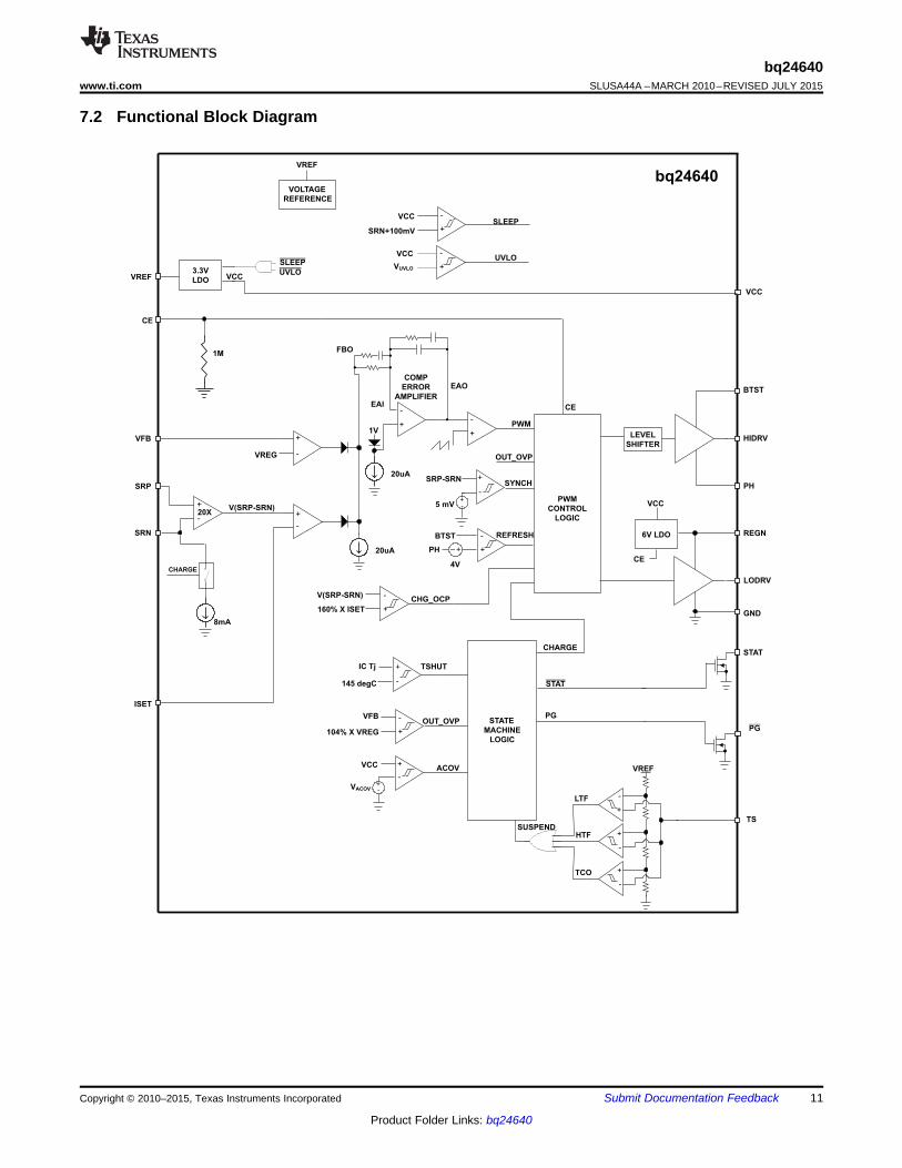
7.1 OverviewThe bq24640 device is a stand-alone, integrated super capacitor charger. The device employs a switched-modesynchronous buck PWM controller with constant switching frequency.
Charging begins in one of two phases (depending upon super capacitor voltage): constant current (fast-chargecurrent regulation), and constant voltage (fast-charge voltage regulation). Constant current can be configuredthrough the ISET pin, allowing for flexibility in the super capacitor charging profile. During charging, theintegrated fault monitors of the device, such as output overvoltage protection (VOV_RISE), thermal shutdown(internal TSHUT and TS pin), and input voltage protection (VACOV and VUVLO), ensure super capacitor safety.
The bq24640 has two status pins (STAT and PG) to indicate the charging status and input voltage (AC adapter)status. These pins can be used to drive LEDs or communicate with a host processor.
Figure 8. Typical Charging Profile
10 Submit Documentation Feedback Copyright © 2010–2015, Texas Instruments Incorporated
Product Folder Links: bq24640
VCC
BTST
HIDRV
PH
REGN
LODRV
GND
TS
CE
VREG
SRP
6V LDO
V(SRP-SRN)
COMP
ERROR
AMPLIFIER
20uA
1V
SRN
STATE
MACHINE
LOGIC
VCC
PH
4V
+_
BTST REFRESH
CE
145 degC
IC Tj TSHUT
SRN+100mV
VCCSLEEP
LEVEL
SHIFTER
+
-
+
-
+
-+
-
+
-
V(SRP-SRN)CHG_OCP
+
-
160% X ISET
SYNCHSRP-SRN
ISET
5 mV20X
OUT_OVP
+
-
104% X VREG
LTF
+
-
HTF
VREF
TCO +
-
+
-
SUSPEND
VCC ACOV+
-
VACOV
CE
VREF
STAT
STAT
3.3V
LDO VCC
bq24640
+
-
+
-UVLO
VUVLO
VCCSLEEP
UVLO
PWM
CONTROL
LOGIC
+
-PWM
+
-
+
-+-
PG
+-
CHARGE
20uA
CHARGE
8mA
OUT_OVP
VOLTAGE
REFERENCE
VREF
PG
1MFBO
EAO
EAI
VFB
VFB
bq24640www.ti.com SLUSA44A –MARCH 2010–REVISED JULY 2015
7.2 Functional Block Diagram
Copyright © 2010–2015, Texas Instruments Incorporated Submit Documentation Feedback 11
Product Folder Links: bq24640

´
ISETCHARGE
SR
VI =
20 R
é ù´ ê úë û
R2V = 2.1V 1 +
OUT R1
bq24640SLUSA44A –MARCH 2010–REVISED JULY 2015 www.ti.com
7.3 Feature Description
7.3.1 Output Voltage RegulationThe bq24640 uses a high-accuracy voltage regulator for the charging voltage. The charge voltage isprogrammed through a resistor-divider from the output to ground, with the midpoint tied to the VFB pin. Thevoltage at the VFB pin is regulated to 2.1 V, giving Equation 1 for the regulation voltage:
where• R2 is connected from VFB to the output, and R1 is connected from VFB to GND. (1)
7.3.2 Output Current RegulationThe ISET input sets the maximum charging current. Output current is sensed by resistor RSR connected betweenSRP and SRN. The full-scale differential voltage between SRP and SRN is 100 mV. Thus, for a 10-mΩ senseresistor, the maximum charging current is 10 A. The equation for charge current is:
(2)
The input voltage range of ISET is from 0 V to 2 V. The SRP and SRN pins are used to sense voltage acrossRSR with default value of 10 mΩ. However, resistors of other values can also be used. A larger sense resistor willgive a larger sense voltage and a higher regulation accuracy, but this comes at the expense of higher conductionloss.
7.3.3 Power UpThe bq24640 uses a sleep comparator to determine if the source of power on the VCC pin is a valid supply tocharge the capacitor. If the VCC voltage is above the UVLO threshold and greater than the SRN voltage, and allother conditions are met, bq24640 will then start to charge (see Enable and Disable Charging). If the SRNvoltage is greater than VCC, the bq24640 enters a low quiescent current sleep mode to minimize current drainfrom the capacitor (<15 µA).
If VCC is below the UVLO threshold, the device is disabled.
7.3.4 Enable and Disable ChargingThe following conditions have to be valid before charge is enabled:• CE is HIGH.• The device is not in undervoltage lockout (UVLO) mode and not in VCCLOWV.• The device is not in sleep mode (that is, VCC > SRN).• The VCC voltage is lower than the AC overvoltage threshold (VCC < VACOV).• 30-ms delay is complete after initial power up.• The REGN LDO and VREF LDO voltages are at the correct levels.• Thermal shutdown (TSHUT) is not valid.• TS fault is not detected.
One of the following conditions will stop ongoing charging:• CE is LOW.• Adapter is removed, thus causing the device to enter VCCLOWV.• The device is in sleep mode (that is, VCC < SRN).• Adapter is over voltage.• The REGN or VREF LDOs voltage are not valid.• TSHUT IC temperature threshold is reached.• TS voltage goes out of range indicating the temperature is too hot or too cold.
12 Submit Documentation Feedback Copyright © 2010–2015, Texas Instruments Incorporated
Product Folder Links: bq24640

p¦o
o o
1=
2 L C
bq24640www.ti.com SLUSA44A –MARCH 2010–REVISED JULY 2015
Feature Description (continued)7.3.5 Automatic Internal Soft-Start Charger CurrentThe charger automatically soft starts the charger regulation current to ensure there is no overshoot or stress onthe output capacitor. The soft start consists of stepping up the charge regulation current into 8 evenly dividedsteps up to the programmed charge current. Each step lasts around 1.6 ms, for a typical rise time of 13 ms. Noexternal components are needed for this function.
7.3.6 Converter OperationThe synchronous buck PWM converter uses a fixed-frequency voltage mode with feed-forward control scheme. Atype III compensation network allows using ceramic capacitors at the output of the converter. The compensationinput stage is connected internally between the feedback output (FBO) and the error amplifier input (EAI). Thefeedback compensation stage is connected between the error amplifier input (EAI) and error amplifier output(EAO). The LC output filter is selected to give a resonant frequency of 12 kHz to 17 kHz, where resonantfrequency, fo, is given by:
(3)
An internal saw-tooth ramp is compared to the internal EAO error control signal to vary the duty-cycle of theconverter. The ramp height is 7% of the input adapter voltage making it always directly proportional to the inputadapter voltage. This cancels out any loop gain variation due to a change in input voltage, and simplifies the loopcompensation. The ramp is offset in order to allow zero percent duty-cycle when the EAO signal is below theramp. The EAO signal is also allowed to exceed the saw-tooth ramp signal in order to get a 100% duty-cyclePWM request. Internal gate drive logic allows achieving 99.98% duty-cycle while ensuring the N-channel upperdevice always has enough voltage to stay fully on. If the BTST pin to PH pin voltage falls below 4.2 V for morethan 3 cycles, then the high-side N-channel power MOSFET is turned off and the low-side N-channel powerMOSFET is turned on to pull the PH node down and recharge the BTST capacitor. Then the high-side driverreturns to 100% duty-cycle operation until the (BTST-PH) voltage is detected to fall low again due to leakagecurrent discharging the BTST capacitor below the 4.2 V, and the reset pulse is issued.
The fixed-frequency oscillator keeps tight control of the switching frequency under all conditions of input voltage,output voltage, charge current, and temperature, simplifying output filter design and keeping it out of the audiblenoise region.
7.3.7 Synchronous and Nonsynchronous OperationThe charger operates in synchronous mode when the SRP-SRN voltage is above 5 mV (0.5-A inductor currentfor a 10-mΩ sense resistor). During synchronous mode, the internal gate drive logic ensures there is break-before-make complimentary switching to prevent shoot-through currents. During the 30-ns dead time where bothFETs are off, the body-diode of the low-side power MOSFET conducts the inductor current. Having the low-sideFET turnon keeps the power dissipation low, and allows safely charging at high currents. During synchronousmode the inductor current is always flowing and converter operates in continuous conduction mode (CCM),creating a fixed two-pole system.
The charger operates in nonsynchronous mode when the SRP-SRN voltage is below 5 mV (0.5-A inductorcurrent on 10-mΩ sense resistor). The charger is forced into nonsynchronous mode when the super capacitorvoltage is lower than 2 V or when the average SRP-SRN voltage is lower than 1.25 mV (125 mA on 10-mΩsense resistor).
During nonsynchronous operation, the body-diode of lower-side MOSFET can conduct the positive inductorcurrent after the high-side N-channel power MOSFET turns off. When the load current decreases and theinductor current drops to zero, the body diode will be naturally turned off and the inductor current will becomediscontinuous. This mode is called Discontinuous Conduction Mode (DCM). During DCM, the low-side N-channelpower MOSFET will turn on when the bootstrap capacitor voltage drops below 4.2 V, then the low-side powerMOSFET will turn off and stay off until the beginning of the next cycle, where the high-side power MOSFET isturned on again. The low-side MOSFET on-time is required to ensure the bootstrap capacitor is alwaysrecharged and able to keep the high-side power MOSFET on during the next cycle.
Copyright © 2010–2015, Texas Instruments Incorporated Submit Documentation Feedback 13
Product Folder Links: bq24640
bq24640SLUSA44A –MARCH 2010–REVISED JULY 2015 www.ti.com
Feature Description (continued)At very low currents during nonsynchronous operation, there may be a small amount of negative inductor currentduring the recharge pulse. The charge must be low enough to be absorbed by the input capacitance. Wheneverthe converter goes into zero percent duty-cycle, the high-side MOSFET does not turn on, and the low-sideMOSFET does not turn on (only recharge pulse) either, and there is almost no discharge from the output.
During the DCM mode the loop response automatically changes and has a single-pole system at which the poleis proportional to the load current, because the converter does not sink current, and only the load provides acurrent sink. This means at very low currents the loop response is slower, as there is less sinking currentavailable to discharge the output voltage.
7.3.8 Input Overvoltage Protection (ACOV)ACOV provides protection to prevent system damage due to high input voltage. When the adapter voltagereaches the ACOV threshold, charge is disabled.
7.3.9 Output Overvoltage ProtectionThe converter will not allow the high-side FET to turn-on until the output voltage goes below 102% of theregulation voltage. This allows one-cycle response to an overvoltage condition – such as occurs when the load isremoved. An 8-mA current sink from SRP-SRN to GND is on during charge and allows discharging the outputcapacitors.
7.3.10 Cycle-by-Cycle Charge Overcurrent ProtectionThe charger has a secondary cycle-to-cycle overcurrent protection. The charger monitors the charge current, andprevents the current from exceeding 160% of the programmed charge current. The high-side gate drive turns offwhen the overcurrent is detected, and automatically resumes when the current falls below the overcurrentthreshold.
7.3.11 Thermal Shutdown ProtectionThe VQFN package has low thermal impedance, which provides good thermal conduction from the silicon to theambient, to keep junctions temperatures low. As added level of protection, the charger converter turns off andself-protects whenever the junction temperature exceeds the TSHUT threshold of 145°C. The charger stays offuntil the junction temperature falls below 130°C.
7.3.12 Temperature QualificationThe controller continuously monitors load temperature by measuring the voltage between the TS pin and GND. Anegative temperature coefficient thermistor (NTC) and an external voltage divider typically develop this voltage.The controller compares this voltage against its internal thresholds to determine if charging is allowed. To initiatea charge cycle, the temperature must be within the V(LTF) to V(HTF) thresholds. If temperature is outside of thisrange, the controller suspends charge and waits until the temperature is within the V(LTF) to V(HTF) range.During the charge cycle the temperature must be within the V(LTF) to V(TCO) thresholds. If temperature isoutside of this range, the controller suspends charge and waits until the temperature is within the V(LTF) toV(HTF) range. The controller suspends charge by turning off the PWM charge FETs. If the TS function is notrequired, R9 and R10 can be the same value so the voltage on TS is 1.65 V with VREF as the reference supply.
14 Submit Documentation Feedback Copyright © 2010–2015, Texas Instruments Incorporated
Product Folder Links: bq24640

VREF
TS
RT 2
RT 1
RTH
103 AT
bq24640
-
VREF
LTF
COLD
V1
VRT1 =
1 1+
RT2 RTH
VREF COLD HOT
LTF TCO
VREF VREFHOT COLD
TCO LTF
1 1V RTH RTH
V VRT2 =
V VRTH 1 RTH 1
V V
æ ö´ ´ ´ -ç ÷
è ø
æ ö æ ö´ - - ´ -ç ÷ ç ÷
è øè ø
CHARGE SUSPENDED CHARGE SUSPENDED
TEMPERATURE RANGE
TO INITIATE CHARGE
TEMPERATURE RANGE
DURING A CHARGE
CYCLE
VLTF
VHTF
GND
VTCO
VLTF
GND
VLTFH VLTFH
VREF VREF
CHARGE SUSPENDED CHARGE SUSPENDED
bq24640www.ti.com SLUSA44A –MARCH 2010–REVISED JULY 2015
Feature Description (continued)
Figure 9. TS Pin, Thermistor Sense Thresholds
Assuming a 103AT NTC thermistor is selector, the value RT1 and RT2 can be determined by using the followingequations:
(4)
(5)
Figure 10. TS Resistor Network
7.3.13 CE (Charge Enable)The CE digital input is used to disable or enable the charge process. A high-level signal on this pin enablescharge, provided all the other conditions for charge are met (see Enabling and Disabling Charge). A high-to-low transition on this pin also resets all timers and fault conditions. There is an internal 1-MΩ pulldown resistoron the CE pin, so if CE is floated the charge will not turn on.
Copyright © 2010–2015, Texas Instruments Incorporated Submit Documentation Feedback 15
Product Folder Links: bq24640

bq24640SLUSA44A –MARCH 2010–REVISED JULY 2015 www.ti.com
Feature Description (continued)7.3.14 PG OutputThe open-drain PG (power good) output indicates when the VCC voltage is present. The open-drain FET turnson whenever bq24640 is not in UVLO mode and not in sleep mode (that is, V(VCC) > V(SRN) and V(VCC) >V(UVLO)). The PG pin can be used to drive an LED or communicate to the host processor.
7.3.15 Charge Status OutputsThe open-drain STAT output indicates various charger operations as shown in Table 2. These status pins can beused to drive LEDs or communicate with the host processor.
NOTEOFF indicates that the open-drain transistor is turned off.
Table 2. STAT Pin DefinitionCHARGE STATE STAT
CE high ONSleep mode OFFCharge Suspend (TS), Input or Output Overvoltage, CE low Blinking
7.4 Device Functional Modes
7.4.1 Constant Current ModeIf the super capacitor voltage is less than the programmed target voltage (that is, VFB pin is less than VFB) whencharging is enabled, then charging will resume in constant current mode. In this mode, the super capacitorcharge current will be constant and regulated as per the ISET and current sense resistor (between SRP andSRN) settings.
7.4.2 Constant Voltage ModeWhen the super capacitor voltage is between the target charge voltage and OVP condition (that is, VFB ≤ VFB pin< VOV_RISE), then the device will be in constant voltage mode. In this mode, the super capacitor voltage will beconstant and regulated as per the VFB setting while the charge current will taper down.
16 Submit Documentation Feedback Copyright © 2010–2015, Texas Instruments Incorporated
Product Folder Links: bq24640

³SAT CHG RIPPLEI I + (1/2) I
apacitor
Cff22 pF
VCC
REGN
BTST
HIDRV
PH
LODRV
GND
SRP
SRN
VFB
VREF
CE
ISET
TS
STAT
PG
Q5SiS412DN
L: 6.8 µ HC1310 mF
RSR10m W
bq24640
C 810 m F
Q4SiS412DN
C 22.2 mF
Adapter
C1210mF
C1 1: 0.1 µ F
C5:1 mFC 41mF
Super C
C 7: 1 mF
R2300 kW
R1105 kW
R7100 kW
R822.1 kW
R99.31 kW
R10430 kW
TempS ensing
10k(SEMITEC103AT - 2)
R1 3 :10 kW
R1 4:10 kW
Adapter
R 112W
R6: 10 W
D2
MBRS540T3
R 5: 100 W
C10.1 m F
PwrPad
D1BAT54
C 910 m F
C 60. 1mF
C10
0.1 m F
bq24640www.ti.com SLUSA44A –MARCH 2010–REVISED JULY 2015
8 Application and Implementation
NOTEInformation in the following applications sections is not part of the TI componentspecification, and TI does not warrant its accuracy or completeness. TI’s customers areresponsible for determining suitability of components for their purposes. Customers shouldvalidate and test their design implementation to confirm system functionality.
8.1 Application InformationThe bq24640 super capacitor charger is ideal for high current charging (up to 10 A). The bq24640EVMevaluation module is a complete charge module for evaluating the bq24640. The application curves were takenusing the bq24640EVM. Refer to the EVM user's guide (SLUU410) for EVM information.
8.2 Typical Application
VIN = 19 V, VOUT = 8.1 V, Icharge = 3 A, Temperature range 0–45°C
Figure 11. Typical Application Schematic
8.2.1 Design RequirementsFor this design example, use the parameters listed in Table 3 as the input parameters.
Table 3. Design ParametersDESIGN PARAMETER EXAMPLE VALUE
AC adapter voltage (VIN) 19 VBattery charge voltage 8.1 VBattery charge current (during constant current phase) 3 A
8.2.2 Detailed Design Procedure
8.2.2.1 Inductor SelectionThe bq24640 has a 600-kHz switching frequency to allow the use of small inductor and capacitor values. Theinductor saturation current must be higher than the charging current (ICHG) plus half the ripple current(IRIPPLE):
(6)
Copyright © 2010–2015, Texas Instruments Incorporated Submit Documentation Feedback 17
Product Folder Links: bq24640
´ ´top DS(on) GD bottom DS(on) GFOM = R Q ; FOM = R Q
2
OUTOUTO 2
IN
V1ΔV = V
V8LC s
æ ö-ç ÷ç ÷¦ è ø
» ´
´
RIPPLECOUT RIPPLE
II = 0.29 I
2 3
´ -CIN CHGI = I D × (1 D)
´ ´ -
¦ ´
INRIPPLE
V D (1 D)I =
s L
bq24640SLUSA44A –MARCH 2010–REVISED JULY 2015 www.ti.com
The inductor ripple current depends on input voltage (VIN), duty cycle (D = VOUT / VIN), switching frequency (fs),and inductance (L):
(7)
The maximum inductor ripple current happens with D = 0.5 or close to 0.5. Usually inductor ripple is designed inthe range of (20–40%) maximum charging current as a trade-off between inductor size and efficiency for apractical design.
8.2.2.2 Input CapacitorInput capacitor must have enough ripple current rating to absorb input switching ripple current. The worst-caseRMS ripple current is half of the charging current when duty cycle is 0.5. If the converter does not operate at50% duty cycle, then the worst case capacitor RMS current ICIN occurs where the duty cycle is closest to 50%and can be estimated by the following equation:
(8)
Low ESR ceramic capacitor such as X7R or X5R is preferred for input decoupling capacitor and must be placedto the drain of the high-side MOSFET and source of the low-side MOSFET as close as possible. Voltage ratingof the capacitor must be higher than normal input voltage level. A 25-V rating or higher capacitor is preferred for20-V input voltage. The 20-μF capacitance is suggested for typical of 3-A to 4-A charging current.
8.2.2.3 Output CapacitorOutput capacitor also must have enough ripple current rating to absorb output switching ripple current. Theoutput capacitor RMS current ICOUT is given:
(9)
The output capacitor voltage ripple can be calculated as follows:
(10)
At certain input/output voltage and switching frequency, the voltage ripple can be reduced by increasing theoutput filter LC.
The bq24640 has internal loop compensator. To get good loop stability, the resonant frequency of the outputinductor and output capacitor must be designed from 12 kHz to 17 kHz. The preferred ceramic capacitor is 25 Vor higher rating, X7R or X5R.
8.2.2.4 Power MOSFETs SelectionTwo external N-channel MOSFETs are used for a synchronous switching charger. The gate drivers are internallyintegrated into the IC with 6 V of gate drive voltage. 30-V or higher voltage rating MOSFETs are preferred for 20-V input voltage and 40-V or higher rating MOSFETs are preferred for 20-V to 28-V input voltage.
Figure-of-merit (FOM) is usually used for selecting proper MOSFET based on a tradeoff between the conductionloss and switching loss. For top side MOSFET, FOM is defined as the product of the ON-resistance of theMOSFET, RDS(ON), and the gate-to-drain charge, QGD. For bottom-side MOSFET, FOM is defined as the productof the ON-resistance of the MOSFET, RDS(ON), and the total gate charge, QG.
(11)
The lower the FOM value, the lower the total power loss. Usually lower RDS(ON) has higher cost with the samepackage size.
18 Submit Documentation Feedback Copyright © 2010–2015, Texas Instruments Incorporated
Product Folder Links: bq24640
SICLoss_driver IN g_totalP = V Q f´ ´
- ´ ´2
bottom CHG DS(on)P = (1 D) I R
REGN plt plton off
on off
V - V VI = , I =
R R
´SW GD GS
1Q = Q + Q
2
SW SWon off
on off
Q Qt = , t =
I I
2Stop CHG DS(on) IN CHG on off
1P = D I R + V I (t + t ) f
2´ ´ ´ ´ ´ ´
bq24640www.ti.com SLUSA44A –MARCH 2010–REVISED JULY 2015
The top-side MOSFET loss includes conduction loss and switching loss. It is a function of duty cycle(D=VOUT/VIN), charging current (ICHG), ON-resistance of the MOSFET (RDS(ON)), input voltage (VIN), switchingfrequency (F), turnon time (ton), and turnoff time (toff):
(12)
The first item represents the conduction loss. Usually MOSFET RDS(ON) increases by 50% with 100ºC junctiontemperature rise. The second term represents the switching loss. The MOSFET turnon and turnoff times aregiven by:
where• QSW is the switching charge• Ion is the turn-on gate driving current• IOFF is the turn-off gate driving current. (13)
If the switching charge is not given in MOSFET datasheet, it can be estimated by gate-to-drain charge (QGD) andgate-to-source charge (QGS):
(14)
Gate driving current total can be estimated by REGN voltage (VREGN), MOSFET plateau voltage (VPLT), totalturnon gate resistance (RON) and turnoff gate resistance ROFF) of the gate driver:
(15)
The conduction loss of the bottom-side MOSFET is calculated with Equation 16 when it operates in synchronouscontinuous conduction mode:
(16)
If the SRP-SRN voltage decreases below 5 mV (the charger is also forced into nonsynchronous mode when theaverage SRP-SRN voltage is lower than 1.25 mV), the low-side FET will be turned off for the remainder of theswitching cycle to prevent negative inductor current.
As a result all the freewheeling current goes through the body-diode of the bottom-side MOSFET. The maximumcharging current in nonsynchronous mode can be up to 0.9 A (0.5 A typical) for a 10-mΩ charging current-sensing resistor considering IC tolerance. Choose the bottom-side MOSFET with either an internal Schottky orbody diode capable of carrying the maximum nonsynchronous mode charging current.
MOSFET gate driver power loss contributes to the dominant losses on controller IC, when the buck converter isswitching. Choosing the MOSFET with a small Qg_total will reduce the IC power loss to avoid thermal shutdown.
where• Qg_total is the total gate charge for both upper and lower MOSFET at 6-V VREGN. (17)
8.2.2.5 Input Filter DesignDuring adapter hot plug-in, the parasitic inductance and input capacitor from the adapter cable form a second-order system. The voltage spike at VCC pin may be beyond IC maximum voltage rating and damage IC. Theinput filter must be carefully designed and tested to prevent an overvoltage event on VCC pin.
There are several methods to damping or limit the overvoltage spike during adapter hot plug-in. An electrolyticcapacitor with high ESR as an input capacitor can damp the over voltage spike well below the IC maximum pinvoltage rating. A high current capability TVS Zener diode can also limit the overvoltage level to an IC safe level.However these two solutions may not have low cost or small size.
Copyright © 2010–2015, Texas Instruments Incorporated Submit Documentation Feedback 19
Product Folder Links: bq24640

AdapterConnector
R1 (2010)
2 W
D1
C1
2.2 Fm
R2 (1206)
4.7 - 30 W
C2
0.1 - 1 Fm
VCC pin
bq24640SLUSA44A –MARCH 2010–REVISED JULY 2015 www.ti.com
A cost effective and small size solution is shown in Figure 12. The R1 and C1 are composed of a damping RCnetwork to damp the hot plug-in oscillation. As a result, the overvoltage spike is limited to a safe level. D1 is usedfor reverse-voltage protection for VCC pin. C2 is the VCC pin decoupling capacitor and must be placed as closeas possible to the VCC pin. The R2 and C2 form a damping RC network to further protect the IC from high dv/dtand high-voltage spike. C2 value must be less than C1 value so R1 can dominant the equivalent ESR value toget enough damping effect for hot plug-in. R1 and R2 package must be sized enough to handle inrush currentpower loss according to resistor manufacturer’s datasheet. The filter components value must always be verifiedwith real application and minor adjustments may must fit in the real application circuit.
Figure 12. Input Filter
8.2.2.6 Inductor, Capacitor, and Sense Resistor Selection GuidelinesThe bq24640 provides internal loop compensation. With this scheme, best stability occurs when the LC resonantfrequency, fo, is approximately 12 kHz to 17 kHz. Table 4 provides a summary of typical LC components forvarious charge currents.
See Inductor Selection for information on controlling ripple current.
Table 4. Typical Inductor, Capacitor, and Sense Resistor Values as a Function of Charge CurrentCHARGE CURRENT 2 A 4 A 6 A 8 A 10 AOutput Inductor Lo 10 µH 6.8 µH 4.7 µH 3.3 µH 3.3 µHOutput Capacitor Co 15 µF 20 µF 30 µF 40 µF 40 µFSense Resistor 10 mΩ 10 mΩ 10 mΩ 10 mΩ 10 mΩ
Table 5. Component List for Typical System Circuit of Figure 11PART DESIGNATOR QTY DESCRIPTIONQ4, Q5 2 N-channel MOSFET, 30 V, 12 A, PowerPAK 1212-8, Vishay-Siliconix, Sis412DND1 1 Diode, Dual Schottky, 30 V, 200 mA, SOT23, Fairchild, BAT54CD2 1 Schottky Diode, 40 V, 5 A, SMC, ON Semiconductor, MBRS540T3D3, D4 2 LED Diode, Green, 2.1 V, 10 mΩ, Vishay-Dale, WSL2010R0100FRSR 1 Sense Resistor, 10 mΩ, 1%, 1 W, 2010, Vishay-Dale, WSL2010R0100FL 1 Inductor, 6.8 μH, 5.5 A, Vishay-Dale IHLP2525CZC8, C9, C12, C13 4 Capacitor, Ceramic, 10 μF, 35 V, 20%, X7RC4, C5 2 Capacitor, Ceramic, 1 μF, 16 V, 10%, X7RC7 1 Capacitor, Ceramic, 1 μF, 50 V, 10%, X7RC1, C6, C11 3 Capacitor, Ceramic, 0.1 μF, 16 V, 10%, X7RC2 1 Capacitor, Ceramic, 2.2 μF, 50 V, 10%, X7RCff 1 Capacitor, Ceramic, 22 pF, 35 V, 10%, X7RC10 1 Capacitor, Ceramic, 0.1 μF, 35 V, 10%, X7RR1 1 Resistor, Chip, 105 kΩ, 1/16 W, 0.5%R2 1 Resistor, Chip, 300 kΩ, 1/16 W, 0.5%R7 1 Resistor, Chip, 100 kΩ, 1/16 W, 0.5%R8 1 Resistor, Chip, 22.1 kΩ, 1/16 W, 0.5%R9 1 Resistor, Chip, 9.31 kΩ, 1/16 W, 1%
20 Submit Documentation Feedback Copyright © 2010–2015, Texas Instruments Incorporated
Product Folder Links: bq24640

bq24640www.ti.com SLUSA44A –MARCH 2010–REVISED JULY 2015
Table 5. Component List for Typical System Circuit of Figure 11 (continued)PART DESIGNATOR QTY DESCRIPTIONR10 1 Resistor, Chip, 430 kΩ, 1/16 W, 1%R11 1 Resistor, Chip, 2 Ω, 1 W, 5%R13, R14 2 Resistor, Chip, 100 kΩ, 1/16 W, 5%R5 1 Resistor, Chip, 100 Ω, 1/16 W, 0.5%R6 1 Resistor, Chip, 10 Ω, 0.25 W, 5%
8.2.3 Application Curves
VIN: 19 V VCAP: 8 V ICHG = 3 A VIN: 19 V VCAP: 8 V ICHG = 3 A
Figure 13. Continuous Conduction Mode Figure 14. Battery Charging Soft Start(by Asserting CE Low to High)
9 Power Supply RecommendationsFor proper operation of bq24640, VCC must be from 5 V to 28 V. To begin charging, VCC must be higher thanSRN by at least 500 mV (otherwise, the device will be in sleep mode). TI recommends an input voltage of atleast 1.5 V to 2 V higher than the super capacitor voltage, taking into consideration the DC losses in the high-side FET (Rdson), inductor (DCR), the input diode drop, and current-sense resistor (between SRP and SRN).Power limit for the input supply must be greater than the maximum power required for super capacitor charging.
10 Layout
10.1 Layout GuidelinesThe switching node rise and fall times should be minimized for minimum switching loss. Proper layout of thecomponents to minimize high frequency current path loop (see Figure 15) is important to prevent electrical andmagnetic field radiation and high frequency resonant problems. Here is a PCB layout priority list for properlayout. Layout PCB according to this specific order is essential.1. Place the input capacitor as close as possible to switching MOSFET supply and ground connections and use
the shortest copper trace connection. These parts must be placed on the same layer of PCB instead of ondifferent layers and using vias to make this connection.
2. The IC must be placed close to the switching MOSFET gate terminals and keep the gate drive signal tracesshort for a clean MOSFET drive. The IC can be placed on the other side of the PCB of switching MOSFETs.
3. Place the inductor input terminal to switching MOSFET output terminal as close as possible. Minimize thecopper area of this trace to lower electrical and magnetic field radiation but make the trace wide enough tocarry the charging current. Do not use multiple layers in parallel for this connection. Minimize parasiticcapacitance from this area to any other trace or plane.
4. The charging current sensing resistor must be placed right next to the inductor output. Route the sense leadsconnected across the sensing resistor back to the IC in same layer, close to each other (minimize loop area)
Copyright © 2010–2015, Texas Instruments Incorporated Submit Documentation Feedback 21
Product Folder Links: bq24640

Charge Current Direction
To SRP and SRN pin
R SNS
To Inductor To Capacitor and Output
Current Sensing Direction
High
Frequency
Current
Path
L1 R1
C3C1 C2PGND
SW V OUT
SuperCapacitor
V IN
bq24640SLUSA44A –MARCH 2010–REVISED JULY 2015 www.ti.com
Layout Guidelines (continued)and do not route the sense leads through a high-current path (see Figure 15 for Kelvin connection for bestcurrent accuracy). Place decoupling capacitor on these traces next to the IC.
5. Place the output capacitor next to the sensing resistor output and ground.6. Output capacitor ground connections must be tied to the same copper that connects to the input capacitor
ground before connecting to system ground.7. Route analog ground separately from power ground and use single ground connection to tie charger power
ground to charger analog ground. Just beneath the IC, use analog ground copper pour, but avoid power pinsto reduce inductive and capacitive noise coupling. Connect analog ground to GND pin using thermal pad asthe single ground connection point to connect analog ground and power ground together, or use a 0-Ωresistor to tie analog ground to power ground (thermal pad must tie to analog ground in this case). A star-connection under thermal pad is highly recommended.
8. It is critical to solder the exposed thermal pad on the backside of the IC package to the PCB ground. Ensurethat there are sufficient thermal vias directly under the IC, connecting to the ground plane on the other layers.
9. Decoupling capacitors must be placed next to the IC pins and make trace connection as short as possible.10. All via size and number should be enough for a given current path.
Refer to the EVM design (SLUU410) for the recommended component placement with trace and via locations.
For the QFN information, refer to Quad Flatpack No-Lead Logic Packages (SCBA017) and QFN/SON PCBAttachment Application Report (SLUA271).
10.2 Layout Examples
Figure 15. High-Frequency Current Path
Figure 16. Sensing Resistor PCB Layout
22 Submit Documentation Feedback Copyright © 2010–2015, Texas Instruments Incorporated
Product Folder Links: bq24640

bq24640www.ti.com SLUSA44A –MARCH 2010–REVISED JULY 2015
11 Device and Documentation Support
11.1 Device Support
11.1.1 Third-Party Products DisclaimerTI'S PUBLICATION OF INFORMATION REGARDING THIRD-PARTY PRODUCTS OR SERVICES DOES NOTCONSTITUTE AN ENDORSEMENT REGARDING THE SUITABILITY OF SUCH PRODUCTS OR SERVICESOR A WARRANTY, REPRESENTATION OR ENDORSEMENT OF SUCH PRODUCTS OR SERVICES, EITHERALONE OR IN COMBINATION WITH ANY TI PRODUCT OR SERVICE.
11.2 Documentation Support
11.2.1 Related DocumentationFor related documentation, see the following:• bq24600/20/40 EVM (HPA421) Multi Cell Synchronous Switch-Mode Charger, SLUU410• Quad Flatpack No-Lead Logic Packages, SCBA017• QFN/SON PCB Attachment, SLUA271
11.3 Community ResourcesThe following links connect to TI community resources. Linked contents are provided "AS IS" by the respectivecontributors. They do not constitute TI specifications and do not necessarily reflect TI's views; see TI's Terms ofUse.
TI E2E™ Online Community TI's Engineer-to-Engineer (E2E) Community. Created to foster collaborationamong engineers. At e2e.ti.com, you can ask questions, share knowledge, explore ideas and helpsolve problems with fellow engineers.
Design Support TI's Design Support Quickly find helpful E2E forums along with design support tools andcontact information for technical support.
11.4 TrademarksE2E is a trademark of Texas Instruments.All other trademarks are the property of their respective owners.
11.5 Electrostatic Discharge CautionThese devices have limited built-in ESD protection. The leads should be shorted together or the device placed in conductive foamduring storage or handling to prevent electrostatic damage to the MOS gates.
11.6 GlossarySLYZ022 — TI Glossary.
This glossary lists and explains terms, acronyms, and definitions.
12 Mechanical, Packaging, and Orderable InformationThe following pages include mechanical, packaging, and orderable information. This information is the mostcurrent data available for the designated devices. This data is subject to change without notice and revision ofthis document. For browser-based versions of this data sheet, refer to the left-hand navigation.
Copyright © 2010–2015, Texas Instruments Incorporated Submit Documentation Feedback 23
Product Folder Links: bq24640
PACKAGE OPTION ADDENDUM
www.ti.com 2-May-2015
Addendum-Page 1
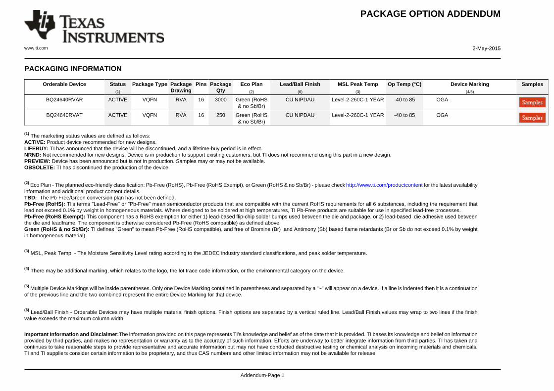
PACKAGING INFORMATION
Orderable Device Status(1)
Package Type PackageDrawing
Pins PackageQty
Eco Plan(2)
Lead/Ball Finish(6)
MSL Peak Temp(3)
Op Temp (°C) Device Marking(4/5)
Samples
BQ24640RVAR ACTIVE VQFN RVA 16 3000 Green (RoHS& no Sb/Br)
CU NIPDAU Level-2-260C-1 YEAR -40 to 85 OGA
BQ24640RVAT ACTIVE VQFN RVA 16 250 Green (RoHS& no Sb/Br)
CU NIPDAU Level-2-260C-1 YEAR -40 to 85 OGA
(1) The marketing status values are defined as follows:ACTIVE: Product device recommended for new designs.LIFEBUY: TI has announced that the device will be discontinued, and a lifetime-buy period is in effect.NRND: Not recommended for new designs. Device is in production to support existing customers, but TI does not recommend using this part in a new design.PREVIEW: Device has been announced but is not in production. Samples may or may not be available.OBSOLETE: TI has discontinued the production of the device.
(2) Eco Plan - The planned eco-friendly classification: Pb-Free (RoHS), Pb-Free (RoHS Exempt), or Green (RoHS & no Sb/Br) - please check http://www.ti.com/productcontent for the latest availabilityinformation and additional product content details.TBD: The Pb-Free/Green conversion plan has not been defined.Pb-Free (RoHS): TI's terms "Lead-Free" or "Pb-Free" mean semiconductor products that are compatible with the current RoHS requirements for all 6 substances, including the requirement thatlead not exceed 0.1% by weight in homogeneous materials. Where designed to be soldered at high temperatures, TI Pb-Free products are suitable for use in specified lead-free processes.Pb-Free (RoHS Exempt): This component has a RoHS exemption for either 1) lead-based flip-chip solder bumps used between the die and package, or 2) lead-based die adhesive used betweenthe die and leadframe. The component is otherwise considered Pb-Free (RoHS compatible) as defined above.Green (RoHS & no Sb/Br): TI defines "Green" to mean Pb-Free (RoHS compatible), and free of Bromine (Br) and Antimony (Sb) based flame retardants (Br or Sb do not exceed 0.1% by weightin homogeneous material)
(3) MSL, Peak Temp. - The Moisture Sensitivity Level rating according to the JEDEC industry standard classifications, and peak solder temperature.
(4) There may be additional marking, which relates to the logo, the lot trace code information, or the environmental category on the device.
(5) Multiple Device Markings will be inside parentheses. Only one Device Marking contained in parentheses and separated by a "~" will appear on a device. If a line is indented then it is a continuationof the previous line and the two combined represent the entire Device Marking for that device.
(6) Lead/Ball Finish - Orderable Devices may have multiple material finish options. Finish options are separated by a vertical ruled line. Lead/Ball Finish values may wrap to two lines if the finishvalue exceeds the maximum column width.
Important Information and Disclaimer:The information provided on this page represents TI's knowledge and belief as of the date that it is provided. TI bases its knowledge and belief on informationprovided by third parties, and makes no representation or warranty as to the accuracy of such information. Efforts are underway to better integrate information from third parties. TI has taken andcontinues to take reasonable steps to provide representative and accurate information but may not have conducted destructive testing or chemical analysis on incoming materials and chemicals.TI and TI suppliers consider certain information to be proprietary, and thus CAS numbers and other limited information may not be available for release.

PACKAGE OPTION ADDENDUM
www.ti.com 2-May-2015
Addendum-Page 2
In no event shall TI's liability arising out of such information exceed the total purchase price of the TI part(s) at issue in this document sold by TI to Customer on an annual basis.

TAPE AND REEL INFORMATION
*All dimensions are nominal
Device PackageType
PackageDrawing
Pins SPQ ReelDiameter
(mm)
ReelWidth
W1 (mm)
A0(mm)
B0(mm)
K0(mm)
P1(mm)
W(mm)
Pin1Quadrant
BQ24640RVAR VQFN RVA 16 3000 330.0 12.4 3.75 3.75 1.15 8.0 12.0 Q1
BQ24640RVAR VQFN RVA 16 3000 330.0 12.4 3.75 3.75 1.15 8.0 12.0 Q1
BQ24640RVAT VQFN RVA 16 250 180.0 12.4 3.75 3.75 1.15 8.0 12.0 Q1
BQ24640RVAT VQFN RVA 16 250 180.0 12.4 3.75 3.75 1.15 8.0 12.0 Q1
PACKAGE MATERIALS INFORMATION
www.ti.com 29-Dec-2017
Pack Materials-Page 1

*All dimensions are nominal
Device Package Type Package Drawing Pins SPQ Length (mm) Width (mm) Height (mm)
BQ24640RVAR VQFN RVA 16 3000 367.0 367.0 35.0
BQ24640RVAR VQFN RVA 16 3000 367.0 367.0 35.0
BQ24640RVAT VQFN RVA 16 250 210.0 185.0 35.0
BQ24640RVAT VQFN RVA 16 250 210.0 185.0 35.0
PACKAGE MATERIALS INFORMATION
www.ti.com 29-Dec-2017
Pack Materials-Page 2


IMPORTANT NOTICE
Texas Instruments Incorporated (TI) reserves the right to make corrections, enhancements, improvements and other changes to itssemiconductor products and services per JESD46, latest issue, and to discontinue any product or service per JESD48, latest issue. Buyersshould obtain the latest relevant information before placing orders and should verify that such information is current and complete.TI’s published terms of sale for semiconductor products (http://www.ti.com/sc/docs/stdterms.htm) apply to the sale of packaged integratedcircuit products that TI has qualified and released to market. Additional terms may apply to the use or sale of other types of TI products andservices.Reproduction of significant portions of TI information in TI data sheets is permissible only if reproduction is without alteration and isaccompanied by all associated warranties, conditions, limitations, and notices. TI is not responsible or liable for such reproduceddocumentation. Information of third parties may be subject to additional restrictions. Resale of TI products or services with statementsdifferent from or beyond the parameters stated by TI for that product or service voids all express and any implied warranties for theassociated TI product or service and is an unfair and deceptive business practice. TI is not responsible or liable for any such statements.Buyers and others who are developing systems that incorporate TI products (collectively, “Designers”) understand and agree that Designersremain responsible for using their independent analysis, evaluation and judgment in designing their applications and that Designers havefull and exclusive responsibility to assure the safety of Designers' applications and compliance of their applications (and of all TI productsused in or for Designers’ applications) with all applicable regulations, laws and other applicable requirements. Designer represents that, withrespect to their applications, Designer has all the necessary expertise to create and implement safeguards that (1) anticipate dangerousconsequences of failures, (2) monitor failures and their consequences, and (3) lessen the likelihood of failures that might cause harm andtake appropriate actions. Designer agrees that prior to using or distributing any applications that include TI products, Designer willthoroughly test such applications and the functionality of such TI products as used in such applications.TI’s provision of technical, application or other design advice, quality characterization, reliability data or other services or information,including, but not limited to, reference designs and materials relating to evaluation modules, (collectively, “TI Resources”) are intended toassist designers who are developing applications that incorporate TI products; by downloading, accessing or using TI Resources in anyway, Designer (individually or, if Designer is acting on behalf of a company, Designer’s company) agrees to use any particular TI Resourcesolely for this purpose and subject to the terms of this Notice.TI’s provision of TI Resources does not expand or otherwise alter TI’s applicable published warranties or warranty disclaimers for TIproducts, and no additional obligations or liabilities arise from TI providing such TI Resources. TI reserves the right to make corrections,enhancements, improvements and other changes to its TI Resources. TI has not conducted any testing other than that specificallydescribed in the published documentation for a particular TI Resource.Designer is authorized to use, copy and modify any individual TI Resource only in connection with the development of applications thatinclude the TI product(s) identified in such TI Resource. NO OTHER LICENSE, EXPRESS OR IMPLIED, BY ESTOPPEL OR OTHERWISETO ANY OTHER TI INTELLECTUAL PROPERTY RIGHT, AND NO LICENSE TO ANY TECHNOLOGY OR INTELLECTUAL PROPERTYRIGHT OF TI OR ANY THIRD PARTY IS GRANTED HEREIN, including but not limited to any patent right, copyright, mask work right, orother intellectual property right relating to any combination, machine, or process in which TI products or services are used. Informationregarding or referencing third-party products or services does not constitute a license to use such products or services, or a warranty orendorsement thereof. Use of TI Resources may require a license from a third party under the patents or other intellectual property of thethird party, or a license from TI under the patents or other intellectual property of TI.TI RESOURCES ARE PROVIDED “AS IS” AND WITH ALL FAULTS. TI DISCLAIMS ALL OTHER WARRANTIES ORREPRESENTATIONS, EXPRESS OR IMPLIED, REGARDING RESOURCES OR USE THEREOF, INCLUDING BUT NOT LIMITED TOACCURACY OR COMPLETENESS, TITLE, ANY EPIDEMIC FAILURE WARRANTY AND ANY IMPLIED WARRANTIES OFMERCHANTABILITY, FITNESS FOR A PARTICULAR PURPOSE, AND NON-INFRINGEMENT OF ANY THIRD PARTY INTELLECTUALPROPERTY RIGHTS. TI SHALL NOT BE LIABLE FOR AND SHALL NOT DEFEND OR INDEMNIFY DESIGNER AGAINST ANY CLAIM,INCLUDING BUT NOT LIMITED TO ANY INFRINGEMENT CLAIM THAT RELATES TO OR IS BASED ON ANY COMBINATION OFPRODUCTS EVEN IF DESCRIBED IN TI RESOURCES OR OTHERWISE. IN NO EVENT SHALL TI BE LIABLE FOR ANY ACTUAL,DIRECT, SPECIAL, COLLATERAL, INDIRECT, PUNITIVE, INCIDENTAL, CONSEQUENTIAL OR EXEMPLARY DAMAGES INCONNECTION WITH OR ARISING OUT OF TI RESOURCES OR USE THEREOF, AND REGARDLESS OF WHETHER TI HAS BEENADVISED OF THE POSSIBILITY OF SUCH DAMAGES.Unless TI has explicitly designated an individual product as meeting the requirements of a particular industry standard (e.g., ISO/TS 16949and ISO 26262), TI is not responsible for any failure to meet such industry standard requirements.Where TI specifically promotes products as facilitating functional safety or as compliant with industry functional safety standards, suchproducts are intended to help enable customers to design and create their own applications that meet applicable functional safety standardsand requirements. Using products in an application does not by itself establish any safety features in the application. Designers mustensure compliance with safety-related requirements and standards applicable to their applications. Designer may not use any TI products inlife-critical medical equipment unless authorized officers of the parties have executed a special contract specifically governing such use.Life-critical medical equipment is medical equipment where failure of such equipment would cause serious bodily injury or death (e.g., lifesupport, pacemakers, defibrillators, heart pumps, neurostimulators, and implantables). Such equipment includes, without limitation, allmedical devices identified by the U.S. Food and Drug Administration as Class III devices and equivalent classifications outside the U.S.TI may expressly designate certain products as completing a particular qualification (e.g., Q100, Military Grade, or Enhanced Product).Designers agree that it has the necessary expertise to select the product with the appropriate qualification designation for their applicationsand that proper product selection is at Designers’ own risk. Designers are solely responsible for compliance with all legal and regulatoryrequirements in connection with such selection.Designer will fully indemnify TI and its representatives against any damages, costs, losses, and/or liabilities arising out of Designer’s non-compliance with the terms and provisions of this Notice.
Mailing Address: Texas Instruments, Post Office Box 655303, Dallas, Texas 75265Copyright © 2017, Texas Instruments Incorporated