body etd 17thdec - ncsu
TRANSCRIPT

Abstract PARTHASARATHY, SRIVATSAN. Interfacing AC Coupled Interconnect design with Rocket I/O compatible FPGA systems. (Under the direction of Dr John Wilson).
As data rates continue to increase, there is an increasing need for reliable high-
density, high-speed interconnect technologies. AC Coupled Interconnect provides a
solution to this problem. The characterizing of high-speed systems in an efficient manner
is an important issue and BER (Bit Error Rate) is one of the most important metrics
utilized to characterize high-speed interconnect technologies.
In this thesis we have developed circuitry that interfaces AC Coupled Interconnect
designs with FPGA based systems that compute the system BER. The FPGA uses Rocket
IO transmitters and receivers to communicate with the test chip. Thus the understanding
of Rocket IO signaling becomes important. Extensive simulations of the Rocket IO
transmitter and receiver models provided by XILINX were carried out across all the
process corners to characterize the system behavior accurately. The interface circuitry
was designed using the TSMC 0.25 Micron process parameters, and the entire design is
validated across a temperature spectrum of -40 C to 120 C and supply voltage of 2.25 V
to 2.75 V. The complete self-test vehicle constitutes the FPGA and the test chip on a
single PCB.
This system is evaluated based on jitter, signal swing and common mode voltage
associated with the signal at the Rocket IO receiver input. HSPICE models for the Rocket
IO transceivers provided by Xilinx allow us to simulate the entire system.
Simulations were carried out to study the impact of ESD on the coupling capacitor
used in the ACCI design. HBM, MM and CDM ESD wave forms were generated in
HSPICE using the standard circuit models provided. The simulation results were helpful
to understand the amount of ESD protection offered by the coupling capacitor.
Capacitance associated with ESD protection becomes a major area for concern with
continuous device scaling. These simulations clearly point to the fact that the coupling
capacitors used in the ACCI system helps to reduce the amount of ESD protection
required. This in turn enables the use of smaller ESD protection circuits with lower
capacitances.

Interfacing AC Coupled Interconnect design with Rocket I/O compatible
FPGA systems
by
Srivatsan Parthasarathy
A thesis submitted to the graduate faculty of
North Carolina State University
in partial fulfillment of the
requirements for the Degree of
Master of Science
Electrical Engineering
Raleigh, North Carolina
2006
Approved by:
__________________________ __________________________
Dr. Paul Franzon Dr.W.Rhett Davis
____________________________________
Dr.John Wilson
Chair of Advisory Committee

To amma and appa
ii

Biography Srivatsan Parthasarathy was born on March 12, 1983 in Chennai a city in southern
India. He graduated from the University of Madras, with a Bachelors degree in
Electronics and Communication Engineering in April 2004. In August 2004, he joined
North Carolina State University as a graduate student. He worked in Sony Ericsson
Mobile Communications, RTP, NC as a RF design co-op from August 2005 to December
2005. While working towards his Masters Degree, he worked on his thesis under the
guidance of Dr.John Wilson. His research interests include high-speed circuit design and
ESD protection for high-speed circuits.
iii

Acknowledgements I thank my parents for all the motivation during the course of this project. It was
their encouragement and love that helped me maintain sanity during the course of this
thesis.
I wholeheartedly acknowledge the efforts of Dr John Wilson, my academic advisor
for providing me with all the possible guidance and encouragement for the completion of
this thesis. I learned the nuances of research in his company. I feel this attribute will help
me immensely in the coming years.
I am very grateful to Dr Paul Franzon for making me realize the importance
continuous progress in a project. I also thank him for his useful comments and time. I am
equally thankful to Dr.W.Rhett Davis for being on the committee and for his valuable
feedback on the thesis document. Special thanks to Manav, Jian, Bruce, Lei and Yongjin
for all those insightful discussions which helped me complete this thesis. I would also
like to thank Prem for his help with the bias circuit design.
Special thanks to my roommates Sreeram, Raju and Suresh for making my stay in
NC State eventful. I sincerely thank Yasaswini for the good cheer and encouragement she
has offered during my graduate study.
iv

v
Contents
List of Figures viii
List of Tables xi
List of Abbreviations xii
1 Introduction....................................................................................................................1
1.1 Overview .................................................................................................................1
1.2 Motivation................................................................................................................2
1.3 Thesis Outline ..........................................................................................................3
2 Literature Review ..........................................................................................................4
2.1 AC Coupled Interconnects.........................................................................................4
2.1.1 Channel Behavior..............................................................................................4
2.1.2 Edge Rate and Coupling Capacitor...................................................................7
2.2 Bit Error Rate Testing................................................................................................8
2.3 Bias Circuit ................................................................................................................9
2.4 Transmission Line Structure on a PCB......................................................................13
2.4.1 Termination schemes ........................................................................................14
3 Rocket IO Signal Environment.....................................................................................18
3.1 Introduction to Rocket IO ..........................................................................................18
3.1.1 Rocket IO Features ...........................................................................................18
3.2 Rocket IO Transceiver ...............................................................................................19
3.2.1 Current Mode Logic..........................................................................................19
3.2.2 Rocket IO Transmitter ......................................................................................20
3.2.3 Rocket IO Receiver...........................................................................................25
4 System Design.................................................................................................................27
4.1 Design Overview (Top Level Hierarchy) .................................................................27
4.2 Programmable Termination Design...........................................................................29

vi
4.3 Front-end Receiver....................................................................................................32
4.4 Limited Swing Differential to Full Swing Single-end conversion ...........................33
4.5 AC Coupled Interconnect Design .............................................................................35
4.5.1 Pulse Signaling.................................................................................................35
4.5.2 ACCI Transmitter ............................................................................................35
4.5.3 Pulse Receiver..................................................................................................36
4.5.4 Summary .........................................................................................................38
4.6 Single end to Differential Conversion ......................................................................38
4.7 Back-end Transmitter................................................................................................40
4.8 Auto adaptive bias design .........................................................................................41
5 Simulation Results ........................................................................................................43
5.1 Simulation test setup .................................................................................................43
5.1.1 Rocket IO Settings ...........................................................................................43
5.2 Top level Simulation setup .......................................................................................43
5.3 Simulation Results ...................................................................................................45
5.3.1 Simulation Results – Front End Receiver........................................................46
5.3.2 Simulation Results – Differential to Single End Converter.............................47
5.3.3 Simulation Results – ACCI TX/CHANNEL/RX ............................................48
5.3.4 Simulation Results – Single-end to Differential Converter .............................50
5.3.5 Simulation Results – Rocket IO Receiver ....................................................52
6 ESD Protection for High Speed Circuits ....................................................................56
6.1Introduction to ESD ........................................................................................56
6.2 ESD Test Models ......................................................................................................57
6.2.1 Human Body Model.........................................................................................57
6.2.2 Machine Model ................................................................................................58
6.2.3 Charged Device Model ....................................................................................59
6.3 MOS Device Physics in High Current High Voltage Region...................................60
6.4 ESD Protection..........................................................................................................62
6.4.1 MOS Based ESD Protection ............................................................................62
6.4.2 ESD Protection Architectures ..........................................................................64
6.5 ACCI and ESD..........................................................................................................64

vii
6.5.1 Issues with Buffer Design for ESD protection ................................................68
6.5.2 Distributed ESD Protection for High Speed Circuits – A Study .....................68
6.6 Impact of CDM on ACCI .........................................................................................69
7 Conclusion .....................................................................................................................73
7.1 Future Work ..............................................................................................................73
Bibliography ...................................................................................................................75
Appendix A.....................................................................................................................78
Appendix B .....................................................................................................................85
List of Figures 1.1: System Level description of the BERT [3]............................................................2
2.1: AC Coupled Interconnect System...........................................................................4
2.2: Capacitively Coupled Interconnect System............................................................5
2.3: Traditional T-Line...................................................................................................5
2.4: Channel Response comparing T-Line and an ACCI channel .................................6
2.5: ACCI Channel.........................................................................................................7
2.6: Impact of Edge Rate on signal Swing.....................................................................8
2.7: A Basic BER Measurement System .......................................................................9
2.8: Circuit to establish supply-independent currents....................................................10
2.9: Plot of reference current versus VDD.....................................................................11
2.10: Transient behavior of reference circuit .................................................................12
2.11: Digital Trimming ..................................................................................................12
2.12: Transmission line models .....................................................................................14
2.13: PI-Termination......................................................................................................16
2.14: T-Termination.......................................................................................................17
3.1: Overview of Rocket IO signal environment ..........................................................18
3.2: Current Mode Logic...............................................................................................20
3.3: Rocket IO transmitter.............................................................................................21
3.4: Impact of Pre-emphasis .........................................................................................23
3.5: Rocket IO TX Eye Diagrams with Different Pre-emphasis levels ........................24
4.1: System Level Representation ................................................................................28
4.2: Digitally Programmable Resistor...........................................................................29
4.3: Resistor Termination..............................................................................................31
4.4: Front-end Receiver Schematic...............................................................................32
4.5: Differential to Single-end converter ......................................................................34
4.6: Simulated VTC/Gain Characteristics.....................................................................34
4.7: ACCI Transmitter ..................................................................................................36
4.8: Pulse Receiver Design [18]....................................................................................37
4.9: Cross coupled inverter VTC ..................................................................................38
viii

4.10: Single end to Differential Conversion .................................................................39
4.11: Transient response depicting equal delays...........................................................39
4.12: Back end Transmitter...........................................................................................41
4.13: Adaptive Bias network.........................................................................................42
5.1: Top level simulation setup.....................................................................................44
5.1(a): Differential Input to Rocket IO TX and Front end RX .....................................45
5.2: Differential Input Eye Pattern ...............................................................................46
5.3: Transient response of the receiver output ..............................................................47
5.4: Differential Eye Diagram of the receiver output ...................................................48
5.5: Eye Diagram and Transient response of the single ended signal ..........................49
5.6: Transient waveform of ACCI channel ..................................................................50
5.7: Eye Diagrams related to ACCI ..............................................................................51
5.8: Transient response/Eye diagram at the output of single-differential converter.....52
5.9: Rocket IO receiver input (Transient response and Eye Diagram) .........................53
5.10: Rocket IO receiver outputs (Transient response and Eye Diagram) ...................55
6.1: HBM ESD Model and associated waveform.........................................................58
6.2: MM ESD Model and associated waveform...........................................................58
6.3: CDM ESD Model and associated waveform.........................................................60
6.4: (a) Generic I-V curve for an NMOS (b) Cross-section of an
NMOS showing the currents in the parasitic NPN transistor ........................60
6.5: Equivalent circuit for the MOSFET including the current source,
substrate resistance and parasitic bipolar transistor [25] .......................................62
6.6: Basic ESD protection structure of the gg-NMOS
showing the parasitic bipolar transistor [7]............................................................63
6.7: Test setup and simulation result for HBM pu66lses..............................................65
6.8: Test setup and simulation result for MM pulses....................................................66
6.9: Test setup and simulation result for CDM pulses..................................................67
6.10: (A) Voltage across coupling capacitor.................................................................70
6.10: (B) Voltage at the end connected to the Buffer ...................................................70
6.11: CDM ESD test setup............................................................................................71
6.12: Impact of discharge path impedance on rise time................................................72
ix

A.1: Front end Receiver................................................................................................78
A.2: Differential to Single-end Converter ....................................................................79
A.3: ACCI Transmitter .................................................................................................80
A.4: ACCI ReceiverA.5: Differential to Single end converter.....................................81
A.6: Back end Transmitter............................................................................................82
A.7: Adaptive Bias Circuit............................................................................................83
B.1: Eye diagram showing working at worst case condition (-40 C) ...........................86
B.2: Butterfly plot at 25 C and -40 C for Cross coupled latch......................................87
B.3: Transient simulation showing Latch functionality................................................88
B.4: Eye diagram showing working at worst case condition (120 C) ..........................89
B.5: Butterfly plot at 25 C and 120 C for Cross coupled latch.....................................90
B.6: Eye diagram showing working at worst case condition (-40 C) ...........................91
B.7: Butterfly plot at 25 C and -40 C for Cross coupled latch......................................92
x

List of Tables
3.1: Rocket IO transmitter parameters ...........................................................................22
3.2: Pre-emphasis Values...............................................................................................23
3.3: Rocket IO receiver parameters ...............................................................................25
3.4: Recommended VTRX for AC/DC Coupling..........................................................26
4.1: Resistor value Calculation for various bits .............................................................30
5.1: Comparing simulated and actual Rocket IO parameters ........................................54
6.1: Short-circuit HBM ESD waveform specifications .................................................57
6.2: Short-circuit MM ESD waveform specifications ...................................................59
6.3: Short-circuit MM ESD waveform specifications ...................................................60
B.1: Design functionality at temperature and Voltage...................................................85
B.2: Design functionality at temperature and Voltage...................................................89
B.3: Design functionality at temperature and Voltage...................................................91
xi

LIST OF ABBREVIATIONS ACCI-AC Coupled Interconnect
BER-Bit Error Rate
BERT-Bit Error Rate Tester
CDM-Charge Device Model
CML-Current Mode Logic
DUT-Device Under Test
EMI-Electromagnetic Interference
ESD-Electrostatic Discharge
FPGA-Field Programmable Gate Array
HBM-Human Body Model
ISI-Inter Symbol Interference
I/O-Input/Output
IC-Integrated Circuit
MM-Machine Model
NRZ-Non Return to Zero
PCB-Printed Circuit Board
PRBS-Pseudo-Random Bit Sequence
RZ-Return to Zero
RX-Receiver
SCL-Source Coupled Logic
SPICE-Simulation Program with Integrated Circuit Emphasis
TX-Transmitter
VTC-Voltage Transfer Characteristic
xii

1
Chapter 1
Introduction
1.1 Overview
The continuous scaling of Integrated circuits has enabled a rapid increase in
operating frequencies, and the increase in circuit density, coupled with synthesis
algorithms, has eased the design of large complex digital systems. The primary
bottleneck in the construction of these complex digital system is the interconnect
technology. This has resulted in the development of novel interconnect techniques that
can handle high data rates and high density off-chip I/Os [1]. As data rates continue to
climb serial communication systems become very dominant. The fundamental advantages
of these systems are that they are less constrained by the timing and alignment problem
that limit a parallel system from being used in high frequency design. Thus signal
integrity becomes a major issue in the design of high speed serial links. Increasing jitter
and reducing jitter budget become the key problems faced in high speed serial link
design. Jitter results in the variation of clock and data edges which in turn results in
higher bit error rates. For the complex digital systems being designed today the minimum
acceptable BER is 10-12
and this should be met for any serial link established between a
transmitter and receiver [2].
BER is defined as the probability of receiving a single bit error at the receiver. This
is the metric that is used to compute the BER of a system. The basic frame work adopted
in this thesis is shown in Figure 1.1. The goal of this thesis is to develop a system that
interfaces the AC Coupled Interconnect design with Rocket IO compatible FRGA’S. This
is being done in order to compute the BER of the AC Coupled Interconnect designs. The
test board consists of power supply, clock oscillators and high-speed connectors to
interface the DUT (ACCI Design) to the FPGA having Rocket IOs. The BER design is
implemented on the FPGA and the interface circuitry is implemented on a separate chip
using TSMC 0.25 micron process parameters. Stripline interconnects are used in between
the FPGA and the chip. It is to be noted that the chip will go on a daughter card which in
turn will be plugged into the main board having the FPGA.

2
Figure 1.1 System Level description of the BERT [3]
The test flow is summarized in the following steps:
1) The specified PRBS pattern is generated by the FPGA
2) This is serialized and sent to the DUT (ACCI Design) through the Rocket IO
transmitter
3) The interface circuitry designed receives the serial data and provides it to the
DUT (ACCI Design)
4) The data from the ACCI design (DUT) is sent back to the FPGA using a custom
designed transmitter.
5) The serial data is received at the Rocket IO receiver. It is than deserialized and
provided to the error detector present in the FPGA.
1.2 Motivation
This thesis is directed by a number of system goals. These include overall jitter,
common mode voltage level for the signal and the total skew associated with the digital
signal. The fundamental challenge is to design interface circuitry that is compatible with

3
Rocket IO signaling levels. The secondary focus of this thesis is to aid in the
development of a complete test system for high speed serial interfaces. This thesis will
provide insights into Rocket IO signaling levels which in turn will allow future designers
to develop a complete self test system.
1.3 Thesis Outline
This thesis is divided into seven chapters. Chapter1 gives an introduction to BER
testing and high-speed serial links. Chapter 2 is the literature review where details are
provided about AC Coupled Interconnect systems, bias circuitry and termination.
Chapter3 goes into the details of Rocket IOs. Chapter4 describes the entire system with
the help of schematics and circuit diagrams. Chapter5 dwells into the simulation results.
Chapter6 describes the impact of ESD on AC Coupled designs and lastly chapter7
concludes.

4
Chapter 2
Literature Review
2.1 AC Coupled Interconnects
The fundamental basis for AC coupling is derived from the assumption that it is
easier to build a dense array of non-contacting AC connections when compared to DC
connections. This is further supported by the fact that all the information pertaining to a
digital signal is present in the AC component [4] [5]. This gives rise to the question of
how to isolate the AC component. The AC component is isolated by blocking the DC
component of the signal by placing a series coupling capacitor or inductor in its path [4]
.The capacitive connection can be created by bringing the two opposing metal plates of
the two different IC'S into close proximity or by direct fabrication on the chip or on a
substrate. An inductive connection can be formed likewise, using two spiral inductors [6].
It has been demonstrated by S. Mick et al that using such non-contacting structures allow
very high density interconnects to be realized [6]. A complete AC coupled system
consists of capacitive or inductive coupling elements, buried solder bumps for DC
connections and transceiver circuits to compensate for the frequency response of the
coupling [5].
Figure 2.1: AC Coupled Interconnect System
2.1.1 Channel Behavior
The two basic implementations for an AC Coupled interconnect system are
capacitive coupling and inductive coupling. In this thesis we have focused our attention

5
on capacitive coupling. The schematic for a capacitively coupled system is shown in
Figure 2.2.
Figure 2.2: Capacitively Coupled Interconnect System
A traditional T-Line sans the coupling capacitor as shown in Figure 2.3 has a low pass
channel response.
Figure 2.3: Traditional T-Line
This limits the channels 3dB bandwidth. On the other hand an ACCI channel as shown in
Figure in 2.4 gives you a band pass response. This is due to the presence of the T-Line,
the series coupling capacitor (Cc) and the parasitic capacitor (Cp). These three elements
create a channel from the TX to the RX with a band pass response. The low pass
characteristics of the channel are defined by the T-Line and the parasitic capacitor where
as the high pass characteristics are defined by the series coupling capacitor. The series
coupling capacitor filters out the low frequency component of the transmitted data. Thus
reducing the ISI and increasing the 3dB channel bandwidth to higher frequencies. This is
depicted in the channel response plot as shown in Figure 2.5 comparing the traditional T-
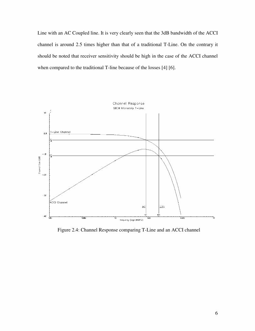
6
Line with an AC Coupled line. It is very clearly seen that the 3dB bandwidth of the ACCI
channel is around 2.5 times higher than that of a traditional T-Line. On the contrary it
should be noted that receiver sensitivity should be high in the case of the ACCI channel
when compared to the traditional T-line because of the losses [4] [6].
Figure 2.4: Channel Response comparing T-Line and an ACCI channel

7
Figure 2.5: ACCI Channel
2.1.2 Edge Rate and Coupling Capacitor
It is observed that a large signal swing at the receiver input will result in a higher
Signal to Noise ration and low BER. In an ACCI system it is the series coupling capacitor
which converts the full swing NRZ signals to RZ pulse signals. Thus it is very important
that the RZ pulses have a sufficiently high signal swing at the receiver. It is observed that
one of the most important factors determining the signal swing at the receiver is the edge
rate of the NRZ input [4]. This is aptly demonstrated in figure 2.6 which shows the
impact of edge rate on signal swing. The experimental setup for this plot was based on
Figure 2.5. It is clearly observed that the signal having the fastest edge rate has the largest
signal swing at the receiver input [4].
A key point is that faster edge rates result in greater signal swing where as the
transition time of the NRZ signal determines the pulse width of the RZ signal at the
receiver input. The best driver designs for ACCI are those that provide fast edge rates and
short pulse durations [7].

8
Figure 2.6: Impact of Edge Rate on signal Swing
2.2 Bit Error Rate Testing
BER (Bit Error Rate) is technically defined as the number of erroneous bits divided
by the total number of bits transmitted, received, or processed over some stipulated
period. It is just one of many statistical measures of a communication link or channel, and
is usually expressed as a negative power of ten [3].
The two key components of a BERT are the serializer block and the deserializer
block. The serializer block accepts parallel data and converts it to a high-speed serial
output. The deserializer block contains a clock and data recovery unit that extracts the
clock from the serial data and adjusts the serial data with respect to the extracted clock.
The data is then demultiplexed to provide a parallel output. It should be noted that the
intrinsic BER should be zero. Signal-to-noise ratio, jitter, EMI, crosstalk are some of the
major factors that affect the BER [3] [8].
9
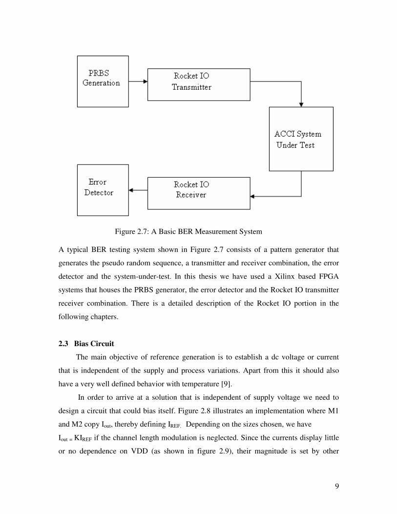
Figure 2.7: A Basic BER Measurement System
A typical BER testing system shown in Figure 2.7 consists of a pattern generator that
generates the pseudo random sequence, a transmitter and receiver combination, the error
detector and the system-under-test. In this thesis we have used a Xilinx based FPGA
systems that houses the PRBS generator, the error detector and the Rocket IO transmitter
receiver combination. There is a detailed description of the Rocket IO portion in the
following chapters.
2.3 Bias Circuit
The main objective of reference generation is to establish a dc voltage or current
that is independent of the supply and process variations. Apart from this it should also
have a very well defined behavior with temperature [9].
In order to arrive at a solution that is independent of supply voltage we need to
design a circuit that could bias itself. Figure 2.8 illustrates an implementation where M1
and M2 copy Iout, thereby defining IREF. Depending on the sizes chosen, we have
Iout = KIREF if the channel length modulation is neglected. Since the currents display little
or no dependence on VDD (as shown in figure 2.9), their magnitude is set by other

10
parameters. It is observed that if all the transistors (M1-M4) operate in the saturation
region and CLM = 0, then the circuit is governed by only one equation, Iout = KIREF. In
order to uniquely define the currents in the circuit we add a resistor as depicted in Figure
2.8 [9].
Figure 2.8: Circuit to establish supply-independent currents
Note that a start-up circuit is included in the Figure 2.8. In any self-biased circuit there
are two possible operating points. The first operating point is based on the assumption
that there will be some finite amount of current flowing in the circuit. The second
possible operating point suggests that there can be a condition where zero current flows
in the circuit. This unwanted state occurs when the gates of transistor M3/M4 are at
ground while the gates of M1/M2 are at VDD. The start-up circuit comes to your rescue
in this state. Now assuming the circuit settles into this unwanted state, the gate of
transistor SU1 is at ground and so it is off. The gate of PMOS SU2 is somewhere in
between VDD and VDD-VTHP. The transistor SU3 behaves like an NMOS switch and
leaks current into the gates of M3/M4 from gates of M1/M2 when turned ON. This
causes the current to snap to the desired state and results in transistor SU3 switching off.
This is due to transistor SU1 turning on. It is imperative that during normal operation the
start-up should not interfere in the circuit’s functionality. The current through transistor

11
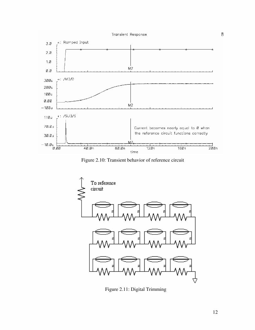
SU3 should be close to zero as shown in Figure 2.10. The problem of start-up requires
some careful analysis and simulations. The supply voltage must be ramped up from zero
in a dc sweep simulation and the behavior of the circuit should be studied with and with
out the start-up [10].
Figure 2.9: Plot of reference current versus VDD
One important aspect to be noted is that MOSFET characteristics and the sheet resistance
vary with process run. Thus there will be a difference in the reference voltage/current
value after fabrication. This difference can be compensated by digitally trimming the
resistors by using fuses. For the circuit in Figure in 2.8 it is observed that decreasing the
resistor value increases the reference voltage and vice versa. To trim the resistor, we start
blowing the fuse across the resistor (electrically or with a LASER). With each blown fuse
we add a finite amount of resistance to the main series resistor. This is pictorially shown
in Figure 2.11 [10].
12
Figure 2.10: Transient behavior of reference circuit
Figure 2.11: Digital Trimming

13
2.4 Transmission Line Structure on a PCB
Transmission line structures seen on a typical PCB consist of conductive traces
buried into a dielectric material with one or more reference planes. The metal in a typical
PCB is usually copper and the dielectric is FR4, which is a type of fiberglass. The two
most common types of transmission lines used in digital designs are microstriplines and
striplines. A microstripline is usually routed on an outside layer of the PCB and has only
one reference plane. A stripline is routed on an inside layer and has two reference planes.
In this thesis we have used single ended and differential transmission line models. This
thesis puts greater emphasis on the differential models because of the complexity
involved and use in Rocket IO channel design.
Figure 2.12 gives a cross sectional view of the differential stripline model. As
mentioned in the previous paragraph a stripline is routed in between two reference planes.
This cross section allows the high frequency current to be distributed equally on both the
top and bottom sides of the signal conductor. Apart from this it also spreads out the
returning current equally among the top and bottom reference planes. Since the current is
spread over a large area conductor losses are minimized.
The other widely used transmission line model is the differential microstripline
model. The cross sectional view of this model is also shown in Figure 2.12. In a
microstripline the signal is exposed to air and has got only a single reference plane. This
makes the line very lossy and is often not utilized for long high speed interconnects.
Microstriplines do not require a via to an inner layer of the PCB, hence are very useful
for dense routing of low speed lines. To interconnect short distances for high-speed
applications, microstriplines can be widened to limit loss. This might also provide
performance advantages over stripline approaches, since striplines require vias to
interconnect signals, reducing bandwidth [11].
For these cross sections shown in Figure 2.12, the dimensions are as follows:
t: Thickness of a signal conductor
w: Width of a signal conductor
s: Spacing between two conductors
h: Height (or thickness) of the dielectric material

14
In addition to this the PCB laminate material has a relative permittivity associated with it
which is labeled Er.
Figure 2.12: Transmission line models
2.4.1 Termination schemes
Transmission lines being designed for this thesis are being driven differentially.
Signals propagating along the line will encounter the differential impedance. This is
lower than the impedance of the line on its own as the influence of the equal and opposite
polarity of the two propagating signals makes the structure behave as though an extra
ground plane has been added vertically between the traces. Though this is an "imaginary"
or "virtual" ground, its influence is the same as a real copper wall.

15
However not all signals on a pair of coupled lines will be differential. The simplest
example to take is electrical noise. One reason for using differential pairs is that a low
level signal can be faithfully reproduced at the receiver in an electrically noisy
environment. As the traces are close, they will suffer from identical noise exposure.
Noise induced on the pair will be of both equal amplitude and polarity. So while the
original signal has equal and opposite polarity and feels the influence of the virtual
ground, the noise will encounter no such ground. In fact as the noise is equal on both
traces, the effect is to slightly increase the impedance of both traces. The impedance seen
by the noise as it propagates is therefore the even mode impedance. Thus it becomes
imperative to terminate both EVEN and ODD mode impedances. Transmission lines need
correct termination in order to preserve signal integrity and minimize reflections [12].
The two commonly used techniques to terminate even and odd mode impedances
simultaneously are PI and T network terminations. Figure 2.12 depicts the PI network
termination. The resistances R1, R2, R3 must be chosen in a way so as to terminate both
even and odd mode impedances. First let’s consider even mode termination where the
voltage at points 1 and 2 are equal. As the net potential difference between the points 1
and 2 is equal to zero no current will be flowing between these two points. Thus R1 and
R2 must be equal to the even mode impedance [13]. To calculate R3 it is required to
evaluate the odd mode propagation. In this case V1 and V2 will be equal in magnitude
but opposite in polarity i.e. V1= -V2. Thus R3 could be split into two equal resistors
with a virtual ground placed in-between. This means that each signal, in odd-mode
propagation, is terminated with a value of R1 (or R2), in parallel with R3 [13]. The
required values of R1 and R3 that may be used to terminate a pair of tightly coupled
transmission lines in both even and odd propagation modes are:
(1) R1 = R2 = Zeven
(2) R3 = 2 * (Zeven) * (Zodd) / (Zeven -Zodd)

16
Figure 2.13: PI-Termination
Figure 2.13 on the other hand shows the T network termination. Let’s initially consider
odd mode termination. In this case the voltage at points 1 and 2 are equal in magnitude
and opposite in direction, a virtual ground can be placed at the point where R3 is
connected. Thus for odd mode propagation the lines are terminated by R1 and R2.
Therefore R1/R2 must be set to the value of odd mode impedance. Moving to even mode
propagation, it’s clear that no current is going to flow between the points 1 and 2. Since
no current will flow between points 1 and 2, the resistor R1 or R2 in series with 2R3 must
equal the even-mode impedance [13]. The subsequent values for R1, R2, and R3 in a T
termination network are:
(!) R1 = R2 = Zodd
(2) R3 = 0.5 * (Zeven -Zodd)

17
Figure 2.14: T-Termination

18
Chapter 3
Rocket IO Signal Environment
3.1 Introduction to Rocket IO
The primary objective of this thesis is to interface the AC Coupled design with
FPGA’s having Rocket IO transmitters and receivers. Rocket IO is a standard that
provides Non-Return to Zero (NRZ) or binary serial communications at up to 3.125 Gb/s
per serial channel. This standard was developed by XILINX and is being used in their
Virtex series FPGA. Figure 3.1 gives a good overview of the Rocket IO signal
environment [11].
Figure 3.1: Overview of Rocket IO signal environment
3.1.1 Rocket IO Features
The Rocket IO transceiver is a highly flexible and programmable system that can be
easily integrated into any Virtex-II Pro design. Following are a few important features
associated with the Rocket IO transceivers [11].

19
- It has a variable speed full duplex transceiver that can operate any where between
600 Mb/s to 3.125 Gb/s.
- Five programmable output swing levels from 800mV to 1600mV peak to peak.
This gives compatibility with other serial systems.
- Four programmable Pre-emphasis levels. This helps minimizing ISI
- It has features for both AC and DC coupling. This gives the advantage of
interfacing with different serial receivers.
- It has programmable 50/75 OHM on-chip tunable resistor. This eliminates the use
of external termination resistors.
- Serial and parallel TX-to-RX internal loopback modes for testing operability
3.2 Rocket IO Transceiver
The Rocket IO transmitter and receiver work on the principle of differential
signaling. It is therefore very important to understand the idea of differential signaling. A
serial differential line will have a positive (V+) and a negative (V-) signal driving it. Thus
the voltage difference between V+ and V- represents the received data. Differential
switching is performed at the crossing of the two signals and thus eliminates the use of a
reference level. This feature operates at a supply voltage of 2.5 [11].
3.2.1 Current Mode Logic
Current Mode Logic is used in the implementation of the Rocket IO transceiver. A
generalized CML circuit shown in Figure 3.2 consists of: 1) Current Sink (NMOS
constant current source to determine the tail current), 2) Pull down network (differential
NMOS pair to perform the logic operation), 3) Resistive load. The required digital logic
is realized by designing the pull down network in a manner so as to switch the tail current
from one branch to another depending on the combination of the differential input signal.
In the branch where current is flowing a resistive voltage drop I*R is developed at the
output and in the other branch where no current flows the output is pulled to VDD
(supply voltage). The output signal swing thus depends totally on the tail current and the
load resistor value. The prime reason for using CML in high-speed designs is that the
load capacitances have to be charged or discharged by an amount equal to the signal

20
swing. This ensures faster switching. The other big reason being the constant current
provided by the NMOS current sink greatly minimizes the switching noise which is
detrimental in high speed design [15] .Apart from this CML is differential in nature this
automatically eliminates the common mode noise [16]
Figure 3.2: Current Mode Logic
3.2.2 Rocket IO Transmitter
Figure 3.3 shows the Rocket IO transceiver design. The basic difference between a
standard CML design and the Rocket IO design is that in this case there is a finite amount
of current flowing through both the branches. Thus one branch will sink more current
than the other. This way the signal and its complement are differentiated. The signal
swing can be improved in two ways: 1) Increase the tail current at the cost of power 2)
Increase the load resistor value. The differential pair output consists of a 50/75 OHM
programmable source resistors. This is useful to minimize reflections.

21
Figure 3.3: Rocket IO transmitter
The Rocket IO transmitter specification is shown in Table 3.1.The terms used in the table
are described below:
VOUT- Differential peak to peak output (TXP-TXN)
VTTX- Output termination voltage
VTCM- Common mode voltage range
VSKEW- Differential output skew

22
Table 3.1: Rocket IO transmitter parameters
Parameter Min Max
VOUT
0.8 V 1.600 V
VTTX
1.8 V 2.625 V
VTCM
1.1 V 2.000 V
VSKEW
15 ps
Pre-Emphasis
The microstrip transmission line model built using the FR4 dielectric is highly lossy
in nature at the desired frequency of operation. The desired frequency of operation is in
the GHZ range. At these frequencies the two main factors that dominate are the dielectric
losses and skin effect. Skin effect is caused due to non uniform electric fields present on
the surface of the conductor. At high frequencies wire resistance increases. This prevents
the electric field from fully penetrating the conductor. These high frequency losses will
result in reflections and decrease in the interconnect bandwidth which in turn will result
in ISI (Inter Symbol Interference).
Pre-emphasis techniques will help to compensate for these high frequency losses.
Pre-emphasis is done by boosting the signal amplitude to create a stronger rising or
falling wave form. This will help in improving the distance over which a signal can be
transmitted over the lossy media and also improve the SNR at the input of the receiver.
This in turn minimizes the BER. The impact of Pre-emphasis is depicted in the Figures
3.4 and 3.5 [11].
In the waveforms shown in Figure 3.4 there are two indicators namely strong low
and strong high. A strong high level shows that the magnitude of the signal at that point
of time is greater than the normal level. The extant of the strong high level indicates the
amount of pre-emphasis. It is observed that pre-emphasis settings should not be set very
high in the case of very short links. The impact of having a very high pre-emphasis
setting can be clearly seen in the eye diagram as shown in Figure 3.5. It is clear that a
very high setting will have an adverse impact on the overall BER. Thus the pre-emphasis

23
levels should be set after careful simulation of the entire system [11]. The four levels of
pre-emphasis are shown in Table 3.2
Table 3.2: Pre-emphasis Values.
Attribute Value Emphasis (%)
0 10
1 20
2 25
3 33
Figure 3.4: Impact of Pre-emphasis

24
Figure 3.5: Rocket IO TX Eye Diagrams with Different Pre-emphasis levels.

25
3.2.3 Rocket IO Receiver
The receiver computes the difference between the two incoming signals to
determine if a ‘1’ or a ‘0’ has been transmitted. Common mode voltage is an important
parameter to be considered in any kind of receiver design. The common mode voltage
level determines how a receiver reads the incoming signal. For the Rocket IO receiver the
incoming signal should have a common mode value between 0.5 V to 2.5 V. Table 3.3
summarizes all the parameters associated with the Rocket IO receiver. The terms used in
the table are described below:
VIN - Serial input differential Peak to Peak (RXP-RXN)
VICM - Common mode voltage level
TJTOL – Total Jitter tolerance for the received data
VSKEW- Total skew associated with the received differential data.
Table 3.3: Rocket IO receiver parameters.
Parameter Min Max
VIN
0.175 V 2.000 V
VTCM
0.5 V 2.500 V
TJTOL 0.65 UI (*)
VSKEW
75 ps
Notes:
* UI=Unit Interval
The incoming signal can be coupled to the receiver in 2 ways: 1) AC Coupling 2) DC
coupling. AC coupling is generally used if the transmitter being coupled with the Rocket
IO receiver does not belong to the Rocket IO family. In that case there could be a
mismatch in the common mode voltage. By AC coupling the signal to the receiver the
common mode value of the signal is zero and is set at the input of the receiver. The
common mode value is automatically set to around 1.6-1.8 V by adjusting the VTRX

26
value. Capacitors in the range of 0.01µF are preferred for AC coupling. On the other
hand if the transmitter being used belongs to the Rocket IO family than the signal can is
DC coupled to the receiver. The VTRX value in this case is set to 2.5 V. The common
mode voltage will be automatically set to 1.7 V. The Rocket IO differential receiver
produces the best bit-error rates when its common mode voltage falls between 1.6V and
1.8V [11]. The VTRX (Common mode voltage) level for the different environments is
shown in Table 3.4.
Table 3.4: Recommended VTRX for AC/DC Coupling
Coupling VTRX VTTX
AC 1.6-1.8 V 2.5 V
DC 2.5 V 2.5 V

27
Chapter 4
System Design
4.1 Design Overview (Top Level Hierarchy)
The primary motive in this thesis is to design circuitry that interfaces the ACCI
design with Rocket IO compatible FPGA systems. This is done in order to verify the
BER of the ACCI system. The error detector present in the FPGA receives the data
propagated via the ACCI system and computes the BER of the DUT. The top level block
diagram is shown in Figure 4.1.The working of this system is as follows:
- The FPGA transmits serial data at 2.5 Gb/s using the Rocket IO transmitter over a 10cm
differential stripline.
- There is a programmable on-chip termination network that helps to remove any kind of
common mode noise.
- Termination is followed by a front-end receiver designed to receive the 2.5 Gb/s data. It
belongs to the SCL (Source Coupled Logic) family.
- A differential to single end converter follows the front-end receiver. This is designed to
interface the single ended ACCI circuitry with the receiver.
- ACCI design follows this. This is our DUT. The ACCI design consists of a transmitter,
series coupling capacitor, 10cm microstrip line, and a receiver.
- The data coming out of the ACCI design is single ended in nature. In order to interface
this design with the differential receiver present in the FPGA a single ended to
differential converter is designed.
- A backend transmitter follows this to transmit data back to the FPGA over a 10cm
differential stripline.

28
Figure 4.1: System Level Representation

29
In the following sub-sections the individual blocks will be analyzed in a detailed manner.
This will include circuit level representations and supporting results/waveforms.
4.2 Programmable Termination Design
Front end termination is a very important design consideration in this system. The
final BER and jitter constraints are greatly affected by improper termination. Since
resistors are going to be used in the termination it is very essential to develop a
programmable termination system which can be externally adjusted depending on the
process variations and temperature. Figure 4.2 shows the schematic of a resistor that can
be digitally tuned depending on the process variation [17].
Figure 4.2: Digitally Programmable Resistor

30
The resistor value is calculated using this simple formula depending on the value of the
digital control bits V<0> and V<1>. Table 4.1 computes the resistor value for the
different Boolean combinations.
Table 4.1: Resistor value Calculation for various bits
V<0> V<1> Net Resistor Value
0 0
0
11
RR term
=
1 0
0,210
111
dsterm rRRRR +++=
0 1
1,65430
111
dsterm rRRRRRR +++++=
1 1
1,65430,210
1111
dsdsterm rRRRRrRRRR +++++
+++=
Notes
0 – Logic low 1 – Logic high
rds,0 , rds,1 – MOSFET (MO,M1) Resistance in linear region of operation
The control bits are realized using two switches present on the PCB. The switch in turn is
connected to a 2.5 V supply line. When switch1 is ON control bit V<0> is high and when
OFF control bit V<0> is low. Similarly when switch2 is ON control bit V<1> is high and
vice versa.
It is also important to understand how the resistor values rds,0 , rds,1 are computed.
MOSFETS’S in linear region of operation behave as resistors. This is the underlying
principle. The reason being in the linear region of operation the drain to source voltage is
directly proportional to the drain to source current. Equations 4.1-4.3 clearly depict the
functionality of the MOSFET like a resistor. Equation 4.1 gives the MOSFET drain to
source current in the linear region.
( )
−−=
2
2
1dsdsthgsoxnD VVVV
L
WCI µ
(4.1)

31
In the equation 4.1 the drain current and the drain to source voltage have a second order
relationship. If in equation 4.1 Vds ≤ 2 (Vgs-Vth), equation 4.1 transforms to
( )[ ]dsthgsoxnD VVV
L
WCI −≈ µ (4.2)
This indicates that the drain current is a linear function of Vds. Thus an important point
to be observed here is that a MOSFET will behave like a linear resistor only for small
values of Vds. The resistance offered by the MOSFET is computed using equation 4.3.
( )[ ]thgsoxn
on
VVL
WC
R
−
=
µ
1
(4.3)
Figure 4.3 shows the whole termination network
Figure 4.3: Resistor Termination

32
A MOSFET can therefore act as a resistor whose value is controlled by the overdrive
voltage (Vgs-Vth) when the condition Vds ≤ 2 (Vgs-Vth) is met. The design described in
the above Figure 4.3 is used realize a 50 OHM termination.
4.3 Front-end Receiver
The most important entity in this system is the front-end receiver. The proposed
receiver has two stages. Though a single stage receiver is sufficient a two stage receiver
is selected in order to drive the subsequent stages. The receiver stages belong to the SCL
family. Simple source coupled inverters are designed as receivers and their main
functionality is to amplify the incoming signal and feed the signal to the subsequent
stage. Source coupled logic is purely differential in nature. This helps to reject common
mode noise in the signal path as well from the power supply. The SCL designs have a
resistive load as pull up instead of a PMOS load in order to achieve higher gain. Figure
4.4 shows the schematic of the two stage receiver based on source coupled logic.
Figure 4.4: Front-end Receiver Schematic

33
Bandwidth, power and signal swing are the most important parameters in the design of
the source coupled logic circuitry. The pull up resistors R1, R2 (R1=R2) are designed
based on the bandwidth requirements and the load capacitance. The load capacitance is
the source to drain capacitance associated with the subsequent MOSFET which is being
driven. As a general rule of thumb the drain to source capacitance of a MOSFET is
equivalent to twice its width. Once the pull up resistors are designed depending on the
input signal swing and the gain required the tail current is calculated. NMOS M5/M6 is
than designed to achieve this tail current. M1 – M4 should be designed in a way so as to
turn OFF during the lower bound of the input signal. As M1, M2, M3 and M4 are source
coupled, the source voltage (Vp1, Vp2) becomes an important design criteria. Vp1/Vp2
should always be set to a value that is greater than the difference between the lower
bound of the input signal and Vth. This is done so that the lower bound of the input signal
turns OFF the NMOS. Thus MI – M4 are designed to achieve a proper bias level at this
computed Vp1/Vp2 value.
The output signal for this design swings from VDD to VDD- R Itail. In order to
increase the signal swing Itail has to be correspondingly increased. This in turn results in
greater power consumption. Based on the bandwidth and signal swing requirement,
power dissipation is determined.
4.4 Limited Swing Differential to Full Swing Single-end conversion
The ACCI circuitry in the subsequent stage is single ended in nature. Apart from
being single-ended it requires full swing CMOS inputs having rail to rail swing. In order
to convert the received differential Rocket IO signals with limited swing to full swing
single ended signals this block was designed. Figure 4.5 shows the schematic of the
above mentioned design.
Differential amplifier with an active PMOS load and single-end output has a
number of advantages like good common mode rejection and high voltage gain. In the
subsequent ACCI stage the transmitter is designed using a set of inverters stages. These
inverters need full swing CMOS inputs to function correctly. Thus if the input signal
swing to the inverter is not sufficient the inverter will either permanently read it as a zero

34
or a one. In order to understand this we have to analyze the inverter transfer
characteristics in a detailed manner.
Figure 4.5: Differential to Single-end converter
Figure 4.6: Simulated VTC/Gain Characteristics

35
The transfer and gain characteristics of the subsequent stage are shown in Figure 4.6. It is
to be noted that the inverter has a PMOS to NMOS ratio of 9:1. This helps to shift the trip
point of the inverter to 1.52 V. It is observed that my increasing the PMOS to NMOS
ration we can move the trip point. There by increasing the gain. This also helps to shift
the VIH and VIL values. The shifting of the VIL value is of particular interest because the
lower bound of the input signal is closer to that value. An inverter reads any value less
than VIL as a one/high. So it is important that the lower bound of the input signal falls
within this range. Thus this design gives us a full swing single-ended CMOS output that
can serve as an input to the subsequent ACCI transmitter [14].
4.5 AC Coupled Interconnect Design
The basics of AC Coupling have been explained in section 2.1 of Chapter 2. In this
section the circuits involved in AC Coupled Interconnect design are described in great
detail. These include the transmitter and the receiver.
4.5.1 Pulse Signaling
As mentioned in section 2.1 of chapter 2 the band pass response of the ACCI
channel produces return to zero pulses. This minimizes the overall power consumption.
In Figure 2.4 of chapter 2 Cc and Cp are the coupling and parasitic capacitors
respectively. The combination of coupling capacitor and the termination resistor behaves
like a differentiator to convert the full swing Non return to zero (NRZ) data to Return to
zero (RZ) pulses [4] [5]. The coupling capacitors will make the DC levels to zero. Thus
the pulse receiver should be able to bias the pulsed signal and reconvert it back to NRZ
data.
4.5.2 ACCI Transmitter
The ACCI channel is extremely lossy in nature. The channel also has very high
input impedance. Thus it is advantageous to go in for a voltage mode driver when
compared to a current mode driver. The other reason for choosing a voltage mode driver
is to have full swing high edge rate signals that can compensate for the high frequency
losses that occur in the ACCI channel. The other feature of voltage mode driver is that it
only consumes dynamic current. This makes the voltage mode driver consume much
lesser power when compared to a current mode driver. To summarize, the benefits of

36
voltage mode driver are as follows: 1) Faster Edge rates, 2) Lower Dynamic power
dissipation, 3) Inverter design is fairly uncomplicated, 4) Chip area consumed is lower.
Figure 4.7 shows the schematic of the ACCI transmitter [4].
The ACCI transmitter is a series of progressively sized inverters. The rule of thumb
used in progressive sizing is that every stage can drive a subsequent stage whose
transistor sizing is twice the previous. This rule of thumb has not been followed for the
last two pairs of inverters. A 1:1 ratio has been used in order to have a really good edge
rate. As observed in Figure 2.9 of chapter 2 it is very clear that faster edge rates will
result in a better signal swing at the input of the ACCI receiver. Thus the goal of
transmitter design should be to provide signals that have a very high edge rate.
Figure 4.7: ACCI Transmitter
4.5.3 Pulse Receiver
The main functionality of the pulse receiver is to convert the RZ pulses back to NRZ
pulses. In the ACCI design the series coupling capacitor removes the DC component
from the signal. Thus the pulse receiver should have the ability to bias the incoming
signal apart from amplifying it and converting it to NRZ pulses. Figure 4.8 shows the
schematic of the pulse receiver [4] [5].
As mentioned in the previous paragraph the input to the receiver has zero bias and it
needs to be set. This is achieved by using an inverter with negative feedback (M6-M7).
Apart from biasing the input signal this design also serves the purpose of amplifying it.
The negative feedback structure also helps to keep the inverter in the high gain region.
The bias voltage set by this negative feedback is vulnerable to the incoming signal width
and swing. It is not very accurate. In order to overcome this problem we have the NMOS

37
M8 tied to VDD that provides a constant feedback that stabilizes the bias voltage. This
feedback is not very strong [4] [18]
A cross coupled inverter is used to perform the latching operation. It is very useful
to understand the working of a cross coupled inverter. A cross coupled inverter is a
bistable circuit with two stable stages, each corresponding to one logic level. Figure 4.9
shows the VTC of a cross coupled inverter. The circuit has three possible operation
points (A, B, C). C is an unstable operating point. If an inverter is biased at C there is a
chance that even a small deviation will result in the operating point being moved from its
original bias. Hence it is very rare to see a cross coupled inverter biased at C.
Figure 4.8: Pulse Receiver Design [18]
Operating points with this property are termed metastable. Therefore the two stable
operating points are A and B. The loop gain is less than unity at these points. Even a large
deviation will not cause the operating point to move from its original bias [14].
In order to move from one state to another the circuit should be switched from
operating point A to B. This is achieved my temporarily increasing the loop gain beyond
unity by using a trigger at the input. In this case the trigger is the incoming data signal.
The trigger will force the loop to have a gain more than unity. For example assume the
latch has stored a 1 and is in position A (Input=0, Output=1). If the incoming trigger
(Data) is 0 the latch will continue to remain in the same state. If a 1 is encountered than
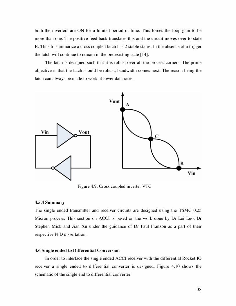
38
both the inverters are ON for a limited period of time. This forces the loop gain to be
more than one. The positive feed back translates this and the circuit moves over to state
B. Thus to summarize a cross coupled latch has 2 stable states. In the absence of a trigger
the latch will continue to remain in the pre existing state [14].
The latch is designed such that it is robust over all the process corners. The prime
objective is that the latch should be robust, bandwidth comes next. The reason being the
latch can always be made to work at lower data rates.
Figure 4.9: Cross coupled inverter VTC
4.5.4 Summary
The single ended transmitter and receiver circuits are designed using the TSMC 0.25
Micron process. This section on ACCI is based on the work done by Dr Lei Luo, Dr
Stephen Mick and Jian Xu under the guidance of Dr Paul Franzon as a part of their
respective PhD dissertation.
4.6 Single ended to Differential Conversion
In order to interface the single ended ACCI receiver with the differential Rocket IO
receiver a single ended to differential converter is designed. Figure 4.10 shows the
schematic of the single end to differential converter.

39
Figure 4.10: Single end to Differential Conversion
Figure 4.11: Transient response depicting equal delays
The key feature in the design of this converter is to minimize the amount of skew
between the two signals. This is achieved by making the delays equal in both Path1 and
40
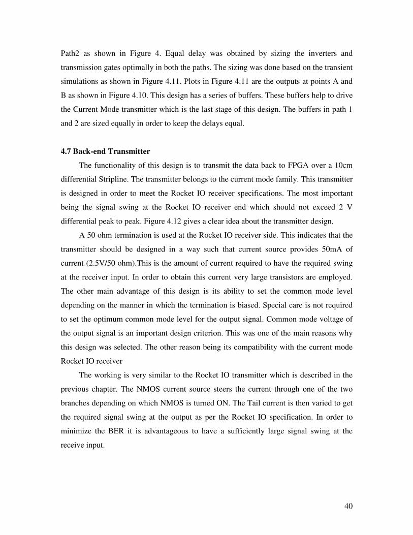
Path2 as shown in Figure 4. Equal delay was obtained by sizing the inverters and
transmission gates optimally in both the paths. The sizing was done based on the transient
simulations as shown in Figure 4.11. Plots in Figure 4.11 are the outputs at points A and
B as shown in Figure 4.10. This design has a series of buffers. These buffers help to drive
the Current Mode transmitter which is the last stage of this design. The buffers in path 1
and 2 are sized equally in order to keep the delays equal.
4.7 Back-end Transmitter
The functionality of this design is to transmit the data back to FPGA over a 10cm
differential Stripline. The transmitter belongs to the current mode family. This transmitter
is designed in order to meet the Rocket IO receiver specifications. The most important
being the signal swing at the Rocket IO receiver end which should not exceed 2 V
differential peak to peak. Figure 4.12 gives a clear idea about the transmitter design.
A 50 ohm termination is used at the Rocket IO receiver side. This indicates that the
transmitter should be designed in a way such that current source provides 50mA of
current (2.5V/50 ohm).This is the amount of current required to have the required swing
at the receiver input. In order to obtain this current very large transistors are employed.
The other main advantage of this design is its ability to set the common mode level
depending on the manner in which the termination is biased. Special care is not required
to set the optimum common mode level for the output signal. Common mode voltage of
the output signal is an important design criterion. This was one of the main reasons why
this design was selected. The other reason being its compatibility with the current mode
Rocket IO receiver
The working is very similar to the Rocket IO transmitter which is described in the
previous chapter. The NMOS current source steers the current through one of the two
branches depending on which NMOS is turned ON. The Tail current is then varied to get
the required signal swing at the output as per the Rocket IO specification. In order to
minimize the BER it is advantageous to have a sufficiently large signal swing at the
receive input.

41
Figure 4.12: Back end Transmitter
4.8 Auto adaptive bias design
The SCL design used to build the front end receiver has resistive load. It is known
that resistors vary heavily with process variations. If the load resistor varies it will have
an instant impact on the output signal swing. The auto bias circuitry will adapt to the
changes in the resistor values as per the process variations. It has been observed that the
resistors vary by as much as +/- 20%. The bias circuitry is shown in Figure 4.13.
It is assumed that Rs and Rl vary in the same direction. Thus if Rs increases Rl also
increases and vice versa. When Rs increases I0 decreases and the product of Rs and I0
remains a constant. So whenever I0 decreases I1 decreases and I2 will eventually
decrease because it’s mirrored from I1. Therefore our objective of making the product of
Rl and I2 a constant has been achieved by the reduction in I2.
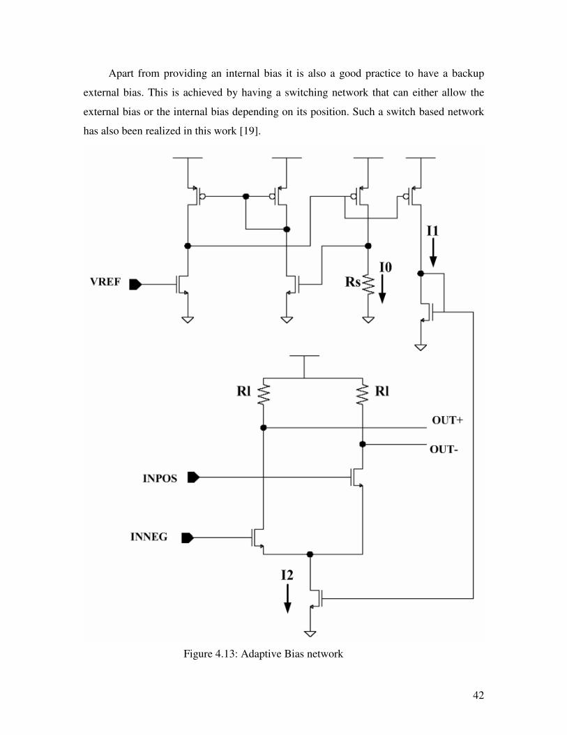
42
Apart from providing an internal bias it is also a good practice to have a backup
external bias. This is achieved by having a switching network that can either allow the
external bias or the internal bias depending on its position. Such a switch based network
has also been realized in this work [19].
Figure 4.13: Adaptive Bias network

43
Chapter 5
Simulation Results
5.1 Simulation test setup
The circuit design was done using the TSMC 0.25 Micron process parameters.
The XILINX Signal Integrity Simulation kit provides the HSPICE models for Rocket IO
transceivers. These include the models for transmitter out buffer, receiver input buffer,
package, interconnects and the input data pattern. The transmitter, receiver and the
package models are encrypted.
The XILINX SIS kit includes two specific files (prbs.inc, datagen.inc) that generate
the PRBS sequence and pre-emphasis sequence. The circuit provided generates a 27 – 1
pseudo random sequence. The pattern has a run length of 7. (Run length is the maximum
number of consecutive 1s or 0s in a pattern). The pattern repeats itself very 127 bits. It is
almost DC balanced with 63 0s and 64 1s in a 127 bit pattern [20].
The circuit in the file datagen.inc produces the pre-emphasis pattern and the data
pattern for the transmitter buffer. The data inputs are reversed and delayed by one bit
period to produce the pre-emphasis pattern. The data input signal has to have a high level
of 2.1V and low level of 1.42V; whereas, the pre-emphasis input signal has to have a
high level of 2.13V and low level of 1.66V. These signaling conventions should be
adhered in order to make the Rocket IO transceiver function properly [20].
5.1.1 Rocket IO Settings
Transmitter output swing 800mV (Maximum 1600mV)
Pre-emphasis 20 %
Transmitter side termination 50 ohms
Data Rate 2Gb/s
Receiver side termination 50 ohms
For further details regarding the settings please refer to tables 3.1, 3.2, and 3.3 of chapter
3. It will give a better picture regarding the different parameters.
5.2 Top level Simulation setup
Figure 5.1 gives the top level setup for this simulation.
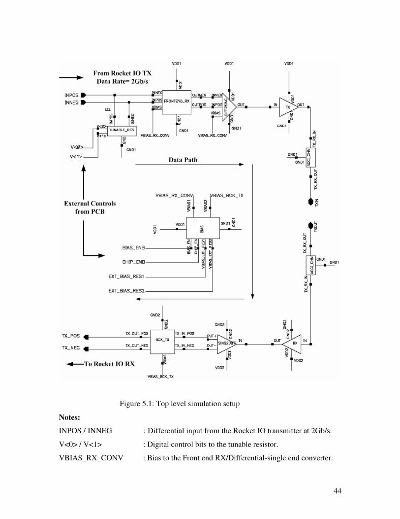
44
Figure 5.1: Top level simulation setup
Notes:
INPOS / INNEG : Differential input from the Rocket IO transmitter at 2Gb/s.
V<0> / V<1> : Digital control bits to the tunable resistor.
VBIAS_RX_CONV : Bias to the Front end RX/Differential-single end converter.

45
VBIAS_BCK_TX : Bias to the back end TX
BIAS_ENB : Lets the user choose between the internal and external bias
CHIP_ENB : To switch ON and OFF the Bias Circuitry.
EXT_BIAS_RES (1/2) : To the external bias resistor that is off chip.
5.3 Simulation Results
The differential input to the Rocket IO TX and the front end receiver is shown in
Figure 5.1. As mentioned in section 5.1 the input to the Rocket IO TX (Data+/Data-)
Figure 5.1 (a): Differential Input to Rocket IO TX and Front end RX
swings from 1.4 to 2.1 V. The input to the front end receiver swing from 1.4-1.8 V. That
is 400mV single ended peak to peak swing or 800mV differential peak to peak swing.
Pre-emphasis is set to 20%. Figure 5.2 shows the eye diagram corresponding to the
differential input pattern.

46
Figure 5.2: Differential Input Eye Pattern
5.3.1 Simulation Results – Front End Receiver
In the previous section the inputs to the Front-end receiver was plotted. As
mentioned in Chapter 4 section 4.3 the output from the receiver swings from 1.8-2.5 V.
There is a 700mV single ended peak to peak swing. It is also important to start keeping
an eye on the jitter budget. The reason being the jitter at the input of the Rocket IO RX is
an important design criterion. The input pattern to the receiver may not represent the
actual jitter. The reason being the SIS kit does not include the models for the core of the
transmitter and the receiver. Only the current mode TX and RX are modeled. Though
some extra jitter has been added to the signal, there might be some discrepancies in the
jitter representation.
Figures 5.3 and 5.4 depict the transient response and the eye diagram associated
with the front end receiver output.

47
Figure 5.3: Transient response of the receiver output.
5.3.2 Simulation Results – Differential to Single End Converter
As explained in Chapter 4 section 4.4 the main goal of this design is to improve the
signal swing and make it compatible with the single ended ACCI TX of the next stage.
The output signal swings from around 700mV to 2.3 V. This signal is subsequently fed to
a specially designed inverter whose trip point is shifted in order to get full swing CMOS
outputs. The jitter at this point is calculated to be 68ps. It should be noted that the total
jitter of the entire system should not exceed 300ps. Figure 5.5 depicts the transient
response and the eye diagram associated with the output of the differential to single
ended converter.

48
Figure 5.4: Differential Eye Diagram of the receiver output
5.3.3 Simulation Results – ACCI TX/CHANNEL/RX
The ACCI transient response is shown in Figure 5.6. The Eye Diagrams associated
with the respective signals are shown in Figure 5.7. The coupling capacitor size used for
the simulation is 450fF. A 10cm Microstripline is used as the channel. 50ohm termination
is used at both the transmitter and the receiver side. The bond wire inductance used in
this case is 2nH. The bond pad capacitance values used in simulations are 200fF. The
parasitic capacitance associated with the coupling capacitors is equal to 100fF. Figure 2.4
depicts the ACCI channel. The signal swing at the receiver is around 110mV and the
common mode level set by the auto bias circuitry is equal to 1.2 V.

49
Figure 5.5: Eye Diagram and Transient response of the single ended signal

50
Figure 5.6: Transient waveform of ACCI channel
5.3.4 Simulation Results – Single-end to Differential Converter
The differential outputs should have minimal skew. This in order to meet the skew
budget at the Rocket IO receiver input. The transient response shown in Figure 5.7
clearly indicates that the skew is quite minimal. Section 4.5 in chapter 4 gives a detailed
overview of this design.

51
Figure 5.7: Eye Diagrams related to ACCI

52
JITTER
110ps
Figure 5.8: Transient response/Eye diagram at the output of single ended-differential
converter
5.3.5 Simulation Results – Rocket IO Receiver
The input to the Rocket IO receiver should have a minimum swing of 175mV and a
maximum swing of 2 V differential peak to peak. The jitter at the input should be less
than 300ps. The common mode voltage of the input should be ranging from 0.5V to 2 V.
Figure 5.9 shows the transient response/eye Diagram of the input to the Rocket IO

53
receiver. The results are tabulated in table 5.1 and compared with the Rocket IO
specifications provided by Xilinx.
Figure 5.9: Rocket IO receiver input (Transient response and Eye Diagram)

54
Table 5.1: Comparing simulated and actual Rocket IO parameters
Parameter
Min Max From
Simulation
VIN 0.175 V 2.000 V 1.5 V
VTCM
0.5 V 2.500 V 1.1 V
TJTOL 0.65 UI (*) 95 ps
VSKEW
75 ps 15 ps
Notes:
UI=Unit Interval (500ps)
VIN - Serial input differential Peak to Peak (RXP-RXN)
VTCM - Common mode voltage level
TJTOL - Total Jitter tolerance for the received data
VSKEW - Total skew associated with the received differential data.
Figure 5.10 shows the Rocket IO receiver output. This receiver data is than passed
through an error detector in the FPGA to compute the BER of the ACCI system.
Computing the BER of the system is beyond the scope of this work. It is clear from the
Rocket IO receiver output that most of the system level specifications were met for this
design.
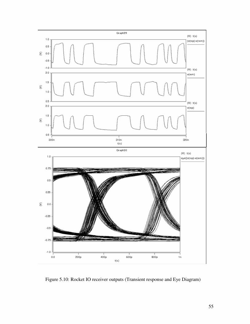
55
Figure 5.10: Rocket IO receiver outputs (Transient response and Eye Diagram)

56
Chapter 6
ESD Protection for High Speed Circuits
6.1 Introduction to ESD
“An electrical surge of a voltage or current that exceeds a device’s rating can trigger
a catastrophic device failure. Such a sudden transfer of charges via induction or direct
contact is defined as electrostatic discharge (ESD)” [26]. ESD can also result in latent
damages that shorten the life of the exposed device instead of immediate failure. To have
a clear understanding of how ESD occurs and what preventive measures to use, it is
important to understand the basic ESD models. There are a number of models that
simulate the ESD conditions that cause direct damage. These include the human body
model (HBM), the machine model (MM), and the charged-device model (CDM). The
HBM is used to simulate a condition where a direct transfer of electrostatic charges takes
place from the human body. In this case the human body acts like a charge-storage
capacitance. The MM approximates the ESD from a charged conductive object, such as a
metallic tool or fixture. The CDM applies to the discharge event between a charged
electronic device and another conductor.
ACCI is a technology that provides a solution for high-density signal I/O and
power/ground pin distribution. It is observed that most of the digital data is carried by AC
components. It is easier to build a dense array of non-contacting AC connections when
compared to DC connections. This is one of the main advantages in using capacitive
coupling for chip to chip connection.
This chapter reviews the impact of ESD on an ACCI design. Previous approaches to
ESD circuit design are discussed, including design theory and specific design examples.
The primary focus of this work is to create electrical models and simulate the effect of the
different ESD pulses on the coupling capacitor and the terminating resistors. After
studying the impact of the ESD pulses, viable protection architectures should be
implemented to offset effects of ESD transients on the ACCI circuit. An important
consideration is to maintain the optimal circuit functionality after the implementation of
the ESD protection circuitry

57
This chapter is divided into 4 subsections. Subsection 6.2 gives a comprehensive
overview of the different ESD test models. A conscious attempt has been made to
highlight the CDM event. The primary reason for this is with the progress of automation
in manufacturing lines, the HBM and MM failures have decreased to a large extant and
major failures would be explained by the CDM ESD event. Subsection 6.3 gives an
overview of the fundamental ESD device phenomena like snap-back and breakdown.
This section also includes a circuit level implementation for modeling MOS snapback
using the HSPICE simulator. Subsection 6.4 starts with a description of the various
devices used in the protection circuitry and subsequently moves on to the various
architectures describing ESD protection. Subsection 6.5 describes the effect of ESD on
ACCI.
6.2 ESD TEST MODELS
6.2.1 Human Body Model
The most well understood ESD mechanism is associated with the human body
caused electrostatic discharge. The HBM ESD event describes a discharge procedure
where in a charged human body contacts a device directly and electrostatic charges
transfer from the human body into the device. HBM can be described on the basis of a
circuit illustrated below in Figure 6.1. This is a military test model and uses a simplified
equivalent circuit where the human charged body is modeled by a charged human body
capacitor Cesd=100pF and typical human body discharging resistance is specified as
Resd =1500Ω. A HBM event is than simulated as ESD from a pre-charged capacitor C
into a DUT via the resistance R. To ensure reliable HBM ESD test data, the MIL-STD-
883E defines a standard short circuit HBM ESD output waveform. In a real world
scenario parasitic effects have a good amount of impact on the transient waveform. All
these parasitics can either be represented as second order or fourth order circuits [31].
Table 6.1: Short-circuit HBM ESD waveform specifications
Parameters T(Rise) T(Decay) ( td) I(Peak)
Specifications <10ns 150ns ~2.75A

58
Figure 6.1: HBM ESD Model and associated waveform
6.2.2 Machine Model
In addition to the human body caused ESD discharge any charged body can
discharge into a DUT without touching it. The most common ESD event of this kind
occurs when metallic machinery contacts the IC components. Typical actions include in-
line inspection and ATE tests. The main difference between the HBM and the MM is that
the parasitic resistance is very low for metallic machinery. This results in a very high
peak current. A basic model is described below. Inductor results in the oscillatory current
waveform.
Figure 6.2: MM ESD Model and associated waveform

59
Table 6.2: Short-circuit MM ESD waveform specifications
6.2.3 Charged Device Model
The CDM applies to the discharge event between a charged electronic device and
another conductor. Triboelectrification, involving the device package or pins, is the
principal cause for the original charge on the device. A CDM-ESD event is a charge
driven phenomena. An IC gets charged by triboelectrification, after contact and
separation with another body. If this charged device comes in contact with a metallic
surface, the charge initially distributed over all the conductive parts of the device is
collected at this point and leaves it via the stress pin within a few nanoseconds [26].
There is a potential drop across the device when a charge passes though it. This voltage
establishes an electric field in the surrounding objects based on the dielectric material
present in the structure. The electric field established results in excessive current which in
turn results in joule heating. Joule heating will melt that specific region. There are two
failure modes associated with high dielectric fields: Dielectric rupture and charge
injection. If the electric field created by the induced voltage is greater than the dielectric
strength of the material it will result in dielectric rupture. Charge injection occurs when
the surface electrons gain sufficient energy to surmount the oxide–silicon energy barrier.
Thus semiconductor devices are damaged by high current densities and high electric
fields. CDM discharge is very rapid and produces a large ESD current because of low
discharge resistance and inductance. The CDM test setup along with the associated
waveforms is shown in Figure 6.3 [26] [21].
The Cesd value is very small in this case because CDM is a self discharging
phenomenon. The Cesd of a device under test will be equal to 7pF approximately. The
parasitic inductance in the discharge path is very unpredictable. That is the precise reason
it is difficult to model a CDM wave form. By definition a CDM waveform should have
very sharp rise times <0.4nS .The reason being the values of resistances and the
Parameters T(Rise) T(Decay) I(Peak)
Specifications ~15-30ns 60-100ns 6-8A
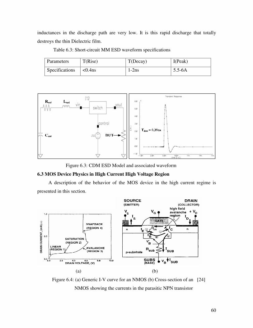
60
inductances in the discharge path are very low. It is this rapid discharge that totally
destroys the thin Dielectric film.
Table 6.3: Short-circuit MM ESD waveform specifications
Figure 6.3: CDM ESD Model and associated waveform
6.3 MOS Device Physics in High Current High Voltage Region
A description of the behavior of the MOS device in the high current regime is
presented in this section.
(a) (b)
Figure 6.4: (a) Generic I-V curve for an NMOS (b) Cross-section of an [24]
NMOS showing the currents in the parasitic NPN transistor
Parameters T(Rise) T(Decay) I(Peak)
Specifications <0.4ns 1-2ns 5.5-6A

61
ESD operation takes place in regions 3 and 4.The mechanism of operation in these
regions involve both avalanche breakdown and turn on of the parasitic lateral NPN
transistor. During high current operation the avalanche generation of carriers in the high
field region near the drain results in hole current into the substrate. This hole current will
result in a voltage drop across the substrate resistance and will eventually result in the
source sub-strate becoming forward biased. The electrons injected from the source into
the sub-strate are collected at the drain forming a lateral NPN bipolar transistor with the
drain as the collector, the source as emitter and the sub-strate as the base. [21] [22] [24]
As the gate voltage goes beyond the MOS threshold it will result in current flowing
between the source and the drain. Therefore this will reduce the amount of sub-strate
current required to turn on the bipolar. As the bipolar turns on, the bipolar current
provides an additional current source for avalanche multiplication thus the magnitude of
drain voltage can reduce and “snapback” is observed when the drain voltage drops to a
minimum sustaining level for the bipolar to be in on condition. Hence the snapback
voltage is a function of the sub-strate resistance and the gain of the intrinsic bipolar
transistor. [21] [22] [24]
The MOSFET operation is broadly divided into 4 regions. Regions 1 and 2 are
governed by the standard MOS equations and modeled in SPICE. Region 3 is the
avalanche breakdown region and the standard MOS equations are no longer valid in this
region. Similarly Region 4 is the bipolar or the snapback region where the standard
models equations do not extend and these regions cannot be modeled in SPICE.
The MOS breakdown region can be modeled in SPICE with a parasitic bipolar
transistor in parallel with the MOS device, together with a current controlled source that
models the avalanche multiplicative effect. [25]
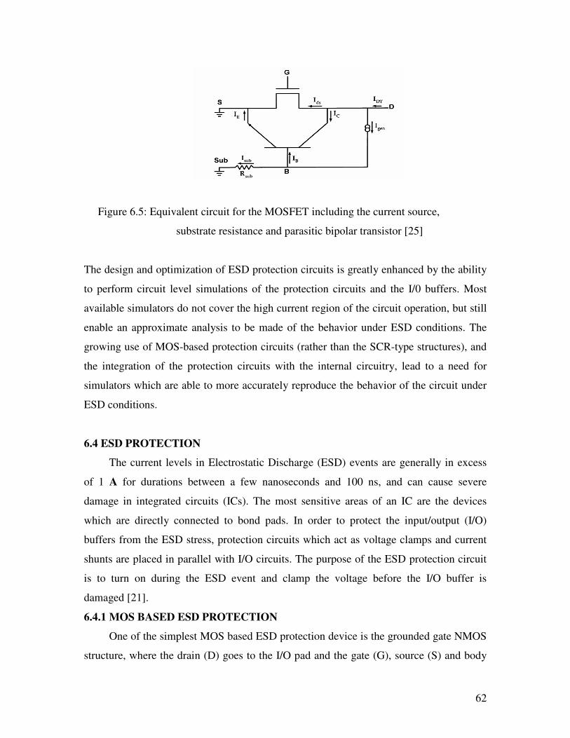
62
Figure 6.5: Equivalent circuit for the MOSFET including the current source,
substrate resistance and parasitic bipolar transistor [25]
The design and optimization of ESD protection circuits is greatly enhanced by the ability
to perform circuit level simulations of the protection circuits and the I/0 buffers. Most
available simulators do not cover the high current region of the circuit operation, but still
enable an approximate analysis to be made of the behavior under ESD conditions. The
growing use of MOS-based protection circuits (rather than the SCR-type structures), and
the integration of the protection circuits with the internal circuitry, lead to a need for
simulators which are able to more accurately reproduce the behavior of the circuit under
ESD conditions.
6.4 ESD PROTECTION
The current levels in Electrostatic Discharge (ESD) events are generally in excess
of 1 A for durations between a few nanoseconds and 100 ns, and can cause severe
damage in integrated circuits (ICs). The most sensitive areas of an IC are the devices
which are directly connected to bond pads. In order to protect the input/output (I/O)
buffers from the ESD stress, protection circuits which act as voltage clamps and current
shunts are placed in parallel with I/O circuits. The purpose of the ESD protection circuit
is to turn on during the ESD event and clamp the voltage before the I/O buffer is
damaged [21].
6.4.1 MOS BASED ESD PROTECTION
One of the simplest MOS based ESD protection device is the grounded gate NMOS
structure, where the drain (D) goes to the I/O pad and the gate (G), source (S) and body
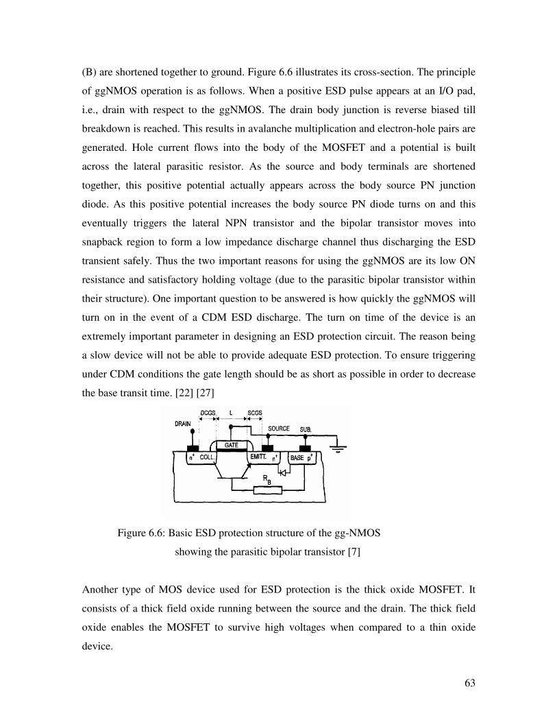
63
(B) are shortened together to ground. Figure 6.6 illustrates its cross-section. The principle
of ggNMOS operation is as follows. When a positive ESD pulse appears at an I/O pad,
i.e., drain with respect to the ggNMOS. The drain body junction is reverse biased till
breakdown is reached. This results in avalanche multiplication and electron-hole pairs are
generated. Hole current flows into the body of the MOSFET and a potential is built
across the lateral parasitic resistor. As the source and body terminals are shortened
together, this positive potential actually appears across the body source PN junction
diode. As this positive potential increases the body source PN diode turns on and this
eventually triggers the lateral NPN transistor and the bipolar transistor moves into
snapback region to form a low impedance discharge channel thus discharging the ESD
transient safely. Thus the two important reasons for using the ggNMOS are its low ON
resistance and satisfactory holding voltage (due to the parasitic bipolar transistor within
their structure). One important question to be answered is how quickly the ggNMOS will
turn on in the event of a CDM ESD discharge. The turn on time of the device is an
extremely important parameter in designing an ESD protection circuit. The reason being
a slow device will not be able to provide adequate ESD protection. To ensure triggering
under CDM conditions the gate length should be as short as possible in order to decrease
the base transit time. [22] [27]
Figure 6.6: Basic ESD protection structure of the gg-NMOS
showing the parasitic bipolar transistor [7]
Another type of MOS device used for ESD protection is the thick oxide MOSFET. It
consists of a thick field oxide running between the source and the drain. The thick field
oxide enables the MOSFET to survive high voltages when compared to a thin oxide
device.

64
6.4.2 ESD PROTECTION ARCHITECTURE
A primary secondary ESD protection scheme is mainly used to protect the I/O
pads. The primary ESD protection circuit is designed to discharge majority of the ESD
current transient. The main function of the secondary ESD protection circuit is to assist
the turn-on of the primary that usually has a relatively high triggering threshold. The
other function of the secondary unit is to ensure sufficient low voltage clamping at the
pad in order to protect the CMOS gate oxide. The operation of this architecture is as
follows. When an ESD transient appears at the bond pads, the secondary ESD protection
unit is turned on initially at a relatively lower voltage and the ESD current flows to the
ground via this shunting path. As the voltage builds across the isolation resistor, the
primary ESD protection unit will be turned on eventually. The key factor in this type of a
design is that the channel impedance of the primary path must be lower than channel
impedance of the secondary path for the primary protection to discharge most of the ESD
current. Typically a primary ESD protection unit can be realized by using thick oxide
NMOS or diode strings, where the capability of handing large ESD current transient is
the most important specification. A ggNMOS is a good secondary ESD protection
structure because of its lower triggering voltage. An important criterion in this case is to
have the holding voltage of the ggNMOS safely below the CMOS gate breakdown limit.
The isolation resistor should be large enough to ensure current limiting function, without
affecting the IC speed performance. [21] [22]
6.5 ACCI and ESD
ACCI is a combination of 3 important components 1) Series coupling capacitor 2)
Parasitic Capacitances and 3) T-Line. The T-line and parasitic capacitors define the low-
pass characteristics while the coupling capacitors define the high-pass characteristics of
the ACCI channel response. The series coupling capacitors filter out the low-frequency
components of transmitted data, thereby reducing ISI and effectively extending channel
bandwidth to higher frequencies. This is a brief introduction to the ACCI Channel.
Our Area of focus in this thesis is to study the behavior of the ACCI Circuit
when an ESD pulse travels from the output pin to the internal circuitry via the coupling
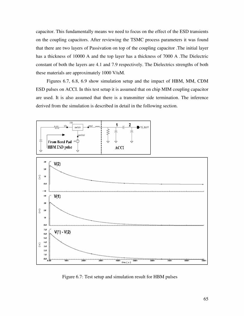
65
capacitor. This fundamentally means we need to focus on the effect of the ESD transients
on the coupling capacitors. After reviewing the TSMC process parameters it was found
that there are two layers of Passivation on top of the coupling capacitor .The initial layer
has a thickness of 10000 A and the top layer has a thickness of 7000 A .The Dielectric
constant of both the layers are 4.1 and 7.9 respectively. The Dielectrics strengths of both
these materials are approximately 1000 V/uM.
Figures 6.7, 6.8, 6.9 show simulation setup and the impact of HBM, MM, CDM
ESD pulses on ACCI. In this test setup it is assumed that on chip MIM coupling capacitor
are used. It is also assumed that there is a transmitter side termination. The inference
derived from the simulation is described in detail in the following section.
Figure 6.7: Test setup and simulation result for HBM pulses

66
Figure 6.8: Test setup and simulation result for MM pulses

67
From Bond Pad
CDM ESD pulseACCI
1 2
V(2)
V(1)
V(1) - V(2)
Figure 6.9: Test setup and simulation result for CDM pulses
After observing the waveforms in Figures 6.7, 6.8, 6.9 following inferences can be
drawn:
1) The MIM on-chip series coupling capacitor will not be damaged by any of the
three ESD pulses. The reason being the voltage across the MIM capacitor never
goes beyond 1000 V which is the breakdown voltage for the dielectric.
2) The series coupling capacitor will offer a sufficient amount of ESD protection
against HBM pulses which have comparatively longer rise times of 10-20 ns. This
validated by the plot which shows that voltage at the other end of the capacitor (2)
in Figure 6.7 is equal to only about 25 V. The really large output buffers will need
minimal ESD protection for such voltages.
3) But as we move to MM and CDM pulses which have a sub-nano seconds rise
times, the series coupling capacitor does not provide good ESD protection. The
reason being the resistance offered by the capacitor decreases with increasing in
frequency. It is very clear from Figures6.8 and 6.9 that voltage at the other end of
68
the capacitor (2) is close to 200 V for CDM and 100 for MM. Thus in these cases
definite ESD protection is required for ACCI designs.
6.5.1 Issues with Buffer Design for ESD protection
Electrostatic discharge and I/O interact at many levels. Usually ESD reliability
imposes additional constraints in the design and layout of the I/O buffers. Fixed finger
width is one of the main constraints imposed by ESD on the design of output buffers.
This can be explained with the help of an example. Assume that a design requires an out
buffers whose width is 200uM. This buffer structure can be realized by using four fingers
each of which is 40uM wide. But this is not possible because of the constraint imposed
by ESD which states that minimum finger width should be 60uM. This means we can
either realize an 180uM design with three fingers or a 240 uM buffer design with four
fingers, both these buffer sizes are 10% under or 20% over the required buffer strength.
The reduced or excess buffer sizing has a direct impact on the output noise and the
network settling time. [21]
6.5.2 Distributed ESD Protection for High Speed Circuits – A Study
Capacitance associated with ESD protection becomes a major area for concern
with continuous device scaling. Apart from scaling the frequency of operation is also
increasing rapidly. As frequency increases the amount of resistance offered by a capacitor
decreases. Thus at high frequencies, the resistance associated with this capacitance
becomes comparable to the 50 ohm characteristic impedance of the board, package and
the transmission line. As a result of this there is severe reflection which in turn decreases
the chip to chip bandwidth. Distributed ESD protection is a possible solution to this
problem as it will enable a low-loss impedance-matched transition from the package to
the chip. A simple resistive model adequately predicts the ESD behavior under stress
according to the charged device and human body models. The large area of the
distributed ESD scheme would limit its application to High Speed serial link design. The
distributed ESD protection is compatible with high-speed layout guidelines, requiring
only low-loss transmission lines in addition to a conventional ESD device. Thus high
bandwidth can be achieved with limited compromise in ESD performance. [29]

69
6.6 Impact of CDM ESD event on ACCI
The coupling capacitor used in ACCI design belongs to the family of metal
insulator metal capacitors. These kinds of capacitors are constructed using metal layers 4
and 5 which in turn form the bottom and top plates of the capacitor. As per the TSMC
0.25 process documentation the IMD (Inter Metal Dielectric) between metal layers 4 and
5 has a thickness of 9492 A. The dielectric constant associated with this dielectric is 4.1.
The dielectric strength of this material is approximately 106 V / cm (1 MV/cm).
The dielectric strength is an intrinsic property of a material. At breakdown, the
electric field frees bound electrons. If the applied electric field is sufficiently high, free
electrons gain energy and start to collide with the other bound electrons resulting in a
process called avalanche breakdown. Breakdown occurs quite abruptly (typically in
nanoseconds) resulting in the formation of an electrically conductive path and a
disruptive discharge through the material. For solid materials, a breakdown event
severely degrades, or even destroys, its insulating capability.
As explained in the previous section it very clear that the coupling capacitor
definitely helps to reduce the impact of the ESD pulse on the output buffer. In this section
the impact of the ESD pulse on the coupling capacitor is studied along with the amount of
protection offered by it. Simulation results are carried out for coupling capacitors whose
size varies from 50 fF to 450 fF.
Thus when coupling capacitors with lower values are being used care must be
taken to verify if the inter metal dielectric are unaffected by the CDM ESD pulse. It is
very clear that if the dielectric strength of the material is 106 V / cm the 9492 A thick
dielectric will breakdown at a voltage of 95 V.
Following conclusions can be drawn from Figure 6.10:-
1) Figure 6.10 (A) clearly shows that the voltage across the coupling capacitor
increases with decreasing capacitance value.
2) Since the IMD (Inter Metal Dielectric) of the coupling capacitor breaks down at
95 V minimal amount of ESD is required to protect the coupling capacitor when
the capacitance value goes below 100ff. This is clearly an important point to be
considered at really high data rates where very small coupling capacitors will be
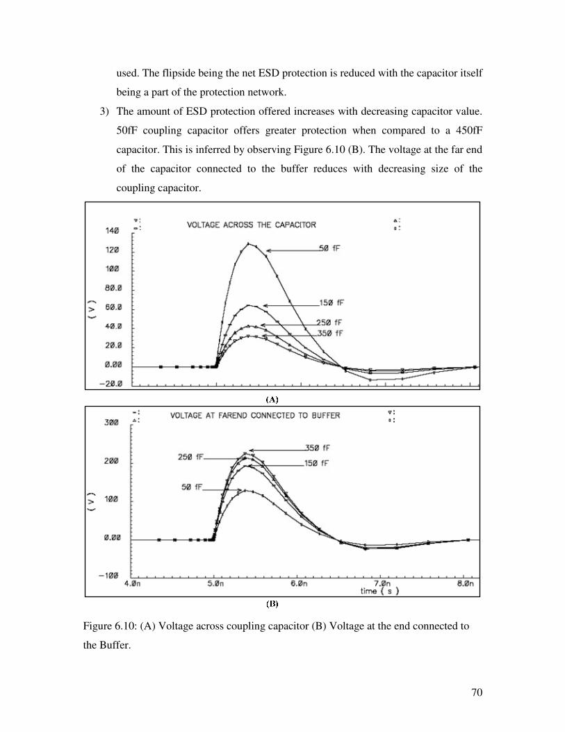
70
used. The flipside being the net ESD protection is reduced with the capacitor itself
being a part of the protection network.
3) The amount of ESD protection offered increases with decreasing capacitor value.
50fF coupling capacitor offers greater protection when compared to a 450fF
capacitor. This is inferred by observing Figure 6.10 (B). The voltage at the far end
of the capacitor connected to the buffer reduces with decreasing size of the
coupling capacitor.
Figure 6.10: (A) Voltage across coupling capacitor (B) Voltage at the end connected to
the Buffer.

71
Figure 6.11: CDM ESD test setup
The next important feature associated with any ESD waveform is its rise time. Therefore
it is important to analyze the behavior of the series coupling capacitor for CDM ESD
pulses with different rise times. In fact it is extremely difficult to predict the rise time of a
CDM ESD pulse accurately because of the difficulty in exactly characterizing the
impedance of the discharge path. The impedance of the discharge path shown in Figure
6.11 mainly depends on the inductance present in the path. Figure 6.12 clearly depicts the
behavior for the various path impedances. The inductance values chosen in this case are 5
nH, 10 nH and 15 nH respectively. Following are the inferences that we can draw from
Figure 6.12:-
1) It is clear from the plot that when the impedance of the discharge path decreases
the rise time of the CDM ESD waveform also decreases. Discharge path with
5 nH inductance has the fastest rise time of 210 ps and the discharge path with
15 nH has the slowest rise time of 400 ps.
2) This means the peak amplitude of the waveform increases with decreasing path
impedance.
3) Voltage across the capacitor increases with decreasing value of the discharge
path impedance.
4) This indicates for lower capacitor values ESD protection is absolutely necessary.
This simulation is carried out for a 150 fF coupling capacitor.

72
Voltage Across Capacitor Cc = 150 fF
Voltage at Near End
Voltage at Far End
Trise = 210 p
Trise = 402 p
Figure 6.12: Impact of discharge path impedance on rise time

73
Chapter 7
Conclusion
A complete system that interfaces AC Coupled Interconnect designs with Rocket
IO based FPGA modules has been designed using TSMC 0.25 Micron process. The
design is supported with robust simulation results across different process corners, supply
voltages and temperatures. A few key Highlights of this design are as follows:
1) HSPICE based Rocket IO models were combined with custom designed circuits. This
allowed us to simulate the entire system.
2) A programmable termination that is digitally controlled has been designed.
Simulations results indicate that this design gives good termination depending on the
control bits selected for all the process corners and for up to +/- 20% variation in resistor
values.
3) The intermediate swing Rocket IO signals are converted to full swing CMOS outputs
with specially designed differential amplifiers and inverters. The inverters were
specifically designed to have a higher trip point.
4) The current design is for single ended ACCI. But it can easily be interfaced with
differential ACCI design.
5) Single end to differential converters were designed to have minimal skew between the
outputs. This was in order to meet the skew constraints at the Rocket IO receiver output.
6) All the specifications at the input of the Rocket IO receiver were met. These include
Jitter, signal swing and common mode level.
7) PVT (Process, Voltage, and Temperature) simulations were carried out to verify the
functionality of the design.
8) Impact of ESD on the ACCI system was studied.
7.1 Future Work
The system design is currently supported only with simulation data. In future the
design should be sent to fabrication and the results verified. The system should also be
verified by interfacing it with Xilinx Virtex-II boards that have Rocket IO transceivers.
The accuracy of the tunable resistor can be improved by using more number of digital

74
control bits. The current system is designed for single ended ACCI circuits. It should be
extended to accommodate differential ACCI design. Phase interpolators can be added in
order to sample the data at various points to eliminate Jitter when longer transmission
lines are used. The system should be simulated with longer transmission lines and the
results should be verified. A robust ESD protection scheme should be added such that it
does not affect the functionality of the design.

75
Bibliography
[1] Interconnects. International Technology Roadmap for Semiconductors, pages 46–50,
2005 Edition.
[2] Gary Ruggles. ARM White Paper on Meeting the High-Speed Serial Link Challenge
November 2006
[3] Manav Shah. Design of a self-test vehicle for AC coupled interconnect technology
Masters thesis, NC State University, 2006
[4] Lei Luo. Capacitively Coupled Chip-to-Chip Interconnect Design. PhD thesis
NC State university, 2005
[5] Stephen Mick, John Wilson, and Paul Franzon. 4 Gbps High-Density AC Coupled
Interconnection. pages 133–140. IEEE Custom Integrated Circuits Conference,
February 2002.
[6] Stephen Mick, Lei Luo, John Wilson, and Paul Franzon. Buried Bump and AC
Coupled Interconnection Technology. volume 27. IEEE Transactions on Advanced
Packaging, February 2004.
[7] L. Luo, J. M. Wilson, S. E. Mick, J. Xu, L. Zhang and P. D. Franzon. A 3Gb/s
AC Coupled Chip-to-Chip Communication using a Low Swing Pulse Receiver.
Pages 522–523. ISSCC Dig. Tech. Papers, February 2005.
[8] ATIS Telecom Glossary 2000. Alliance for Telecommunications Industry Solutions,
February 2000.
[9] Behzad Razavi. Design of Analog CMOS Integrated Circuits. McGraw-Hill,2002
[10] Jacob Baker. CMOS Circuit Design, Layout and Simulation. Wiley, 2006
[11] RocketIO Transceiver User Guide. Xilinx Incorporation, December 2004.
[12] http://www.polarinstruments.com/support/cits/AP157.html
[13] Stephen Hall. High-Speed Digital System Design—A Handbook of Interconnect
Theory and Design Practices. Wiley, 2000

76
[14] Jan Rabey. Digital Integrated Circuits- A Design Perspective. Prentice Hall 2003
[15] J. M. Musicer, J. Rabaey, "MOS Current Mode Logic for Low Power, Low Noise,
CORDIC Computation in Mixed-Signal Environments," Proceedings of the 2000
International Symposium on Low Power Electronics and Design, 2000. ISLPED '00.
July 2000, p. 102-107
[16] M. Mizuno, M. Yamashina, K. Fumta, H. Igura, H. Abiko, K Okabe, A. Ono, and H.
Yamada. A GHz MOS adaptive pipeline technique using MOS Current-mode Logic.
Vol31 ISSCC Dig. Tech. Papers, 1996
[17] Marijan Kumric,Frank Ebert,Roland Ramp,Klaus Welch.Digitally tuneable. On-chip
line termination resistor for 2.5Gbit/s LVDS receiver in 0.25µ standard CMOS
technology
[18] Jian Xu. AC Coupled Interconnect for Inter-chip Communications. Ph D thesis
NC State university,2006
[19] Paul Franzon. Lecture notes ECE 733. NC State university, 2006
[20] Signal Integrity Simulation Kit 3.0 User Guide. Xilinx Incorporation, December
2003
[21] S. Dabral and T. J. Maloney, Basic ESD and I/O Design. New York: Wiley, 1998.
[22]Albert Wang, On-Chip ESD Protection for Integrated Circuits. Boston Kluwer
Publications, 2002.
[23] A.Amerasekara and C.Duvvury, ESD in Silicon Integrated Circuits Wiley, 1995.
[24]A.Amerasekera, S. Ramnswamy, M. Chang, C. Duvvury, “Modeling MOS Snapback
and Parasitic Bipolar Action for Circuit-Level ESD and High Current Simulations”,
Proceedings of 34th Annual IEEE International Reliability Physics, p.318-326, 1996.
[25] X. F. Gao, J. J. Liou, J. Bernier, G. Croft, and A. Ortiz-Conde, “Implementation of a
Comprehensive and Robust MOSFET Model in Cadence SPICE for ESD
Applications”,
[26] Jaesik Lee; Ki-Wook Kim; Yoonjong Huh; Bendix, P.; Sung-Mo Kang, “Chip-level
charged-device modeling and simulation in CMOS integrated circuits”, IEEE
Transactions on Computer-Aided Design of Integrated Circuits and Systems,
Page(s):67 – 81, 2003.

77
[27] G. Meneghesso, J.R.M. Luchies, F. G. Kuper and A.J. Mouthaan, “TURN-ON
SPEED OF GROUNDED GATE NMOS ESD PROTECTION TRANSISTORS”
[28] S.G. Beebe, “Characterization, Modeling, and Design of ESD Protection Circuits,”
Ph.D. Dissertation, Stanford University, 1998.
[29] Kleveland, B.; Maloney, T.J.; Morgan, I.; Madden, L.; Lee, T.H.; Wong, S.S.
“Distributed ESD protection for high-speed integrated circuits”, Electron Device
Letters, IEEE, Page(s):390 – 392, 2000.
[30] F. C. Hsu, P. K. Ko, S. Tan, C. M. Hu, and R. S. Muller, “An analytical
breakdown model for short-channel MOSFET’s,” IEEE Trans. Electron.
Devices, vol. ED-29, Nov. 1982.
[31] MIL-STD-883E, Method 3015.7, ESD sensitivity classification, DOD 1989

78
Appendix A
Circuit Schematic
Figure A.1: Front end Receiver

79
Figure A.2: Differential to Single-end Converter

80
Figure A.3: ACCI Transmitter

81
Figure A.4: ACCI Receiver
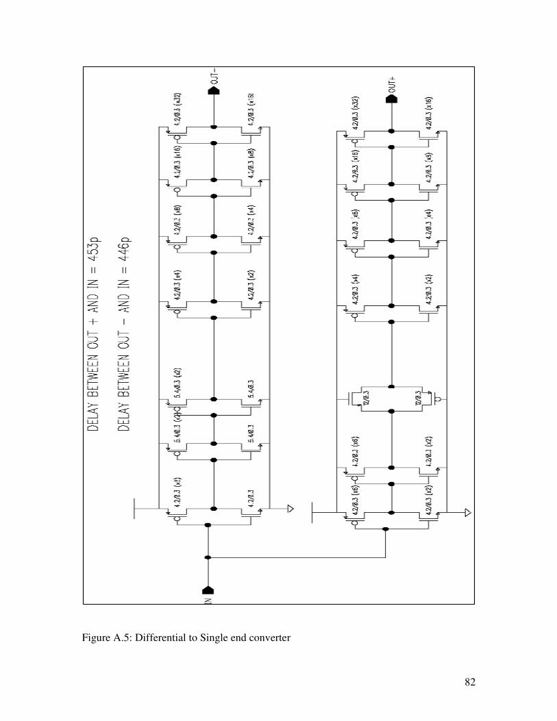
82
Figure A.5: Differential to Single end converter

83
Figure A.6: Back end Transmitter

84
Figure A.7: Adaptive Bias Circuit

85
Appendix B
Process Voltage Temperature Analysis
The design was simulated across three different process corners (SS, FF, TT), three
different supply voltages (2.25, 2.5, 2.75 V) and three different temperatures (-40, 25,120
C). Whenever a process corner failed at a particular temperature supply voltage was
increased or decreased accordingly to get the design working. This gave an insight into
the correct behavior of the design at all the temperatures.
To understand why a design fails at low or high temperature it is important to
understand the working of the MOSFET. At low temperatures the channel resistance goes
down. This results in the reduction of the base transit time for the electrons there by
improving the operating speed of the MOSFET. At high temperatures due to the
enhanced thermal energy, collision among electrons increases and this will result in
increasing the base transit time for the electrons. Thus the device will operate slowly at
low temperatures.
TT Process Corner
Table B.1: Design functionality at temperature and Voltage
-40
25
120
2.02.752.52.25
-40
25
120
2.02.752.52.25

86
From Table B.1 it is very clear that the design at typical (TT) process corner fails at -40 C
for all the voltages. This failure is due to the improper functionality of the cross coupled
latch present in the ACCI receiver. Figure B.1 depicts the working of the design at -40 C.
This is at a much lower supply voltage of 2.0 V.
Latch Output
TT--40 C 2.0 V
Figure B.1: Eye diagram showing working at worst case condition (-40 C)
Figure B.2 depicts the butterfly plot associated with the cross coupled inverter. This lets
us understand the DC behavior of the latch in a clear manner. The butterfly plot gives you
the high and low noise margin values. This helps us determine if the latching operation is
being performed correctly. For example if the input to the latch is high it is expected that
the output is low. But if for some reason the high input falls below the VIH value the
output will have to change its state. This is very clear from the transient analysis depicted
in Figure B.3. A comparison is performed between the working case of the latch and a
non working case. If we observe the non working case it is clearly seen that the latch fails
when ever the input falls below the VIH value.

87
NM High = 1.13 V
NM Low = 1.096 V
25 C TT 2.5 V
NM Low = 1.13 V
-40 C TT 2.5 V
NM High = 1.18 V
Figure B.2: Butterfly plot at 25 C and -40 C for Cross coupled latch

88
Latch Fails
Latch Works
Vih
Cross Coupled Inverter Output
Cross Coupled Inverter Output
Cross Coupled Inverter Input
Cross Coupled Inverter Input
Vih
Figure B.3: Transient simulation showing Latch functionality
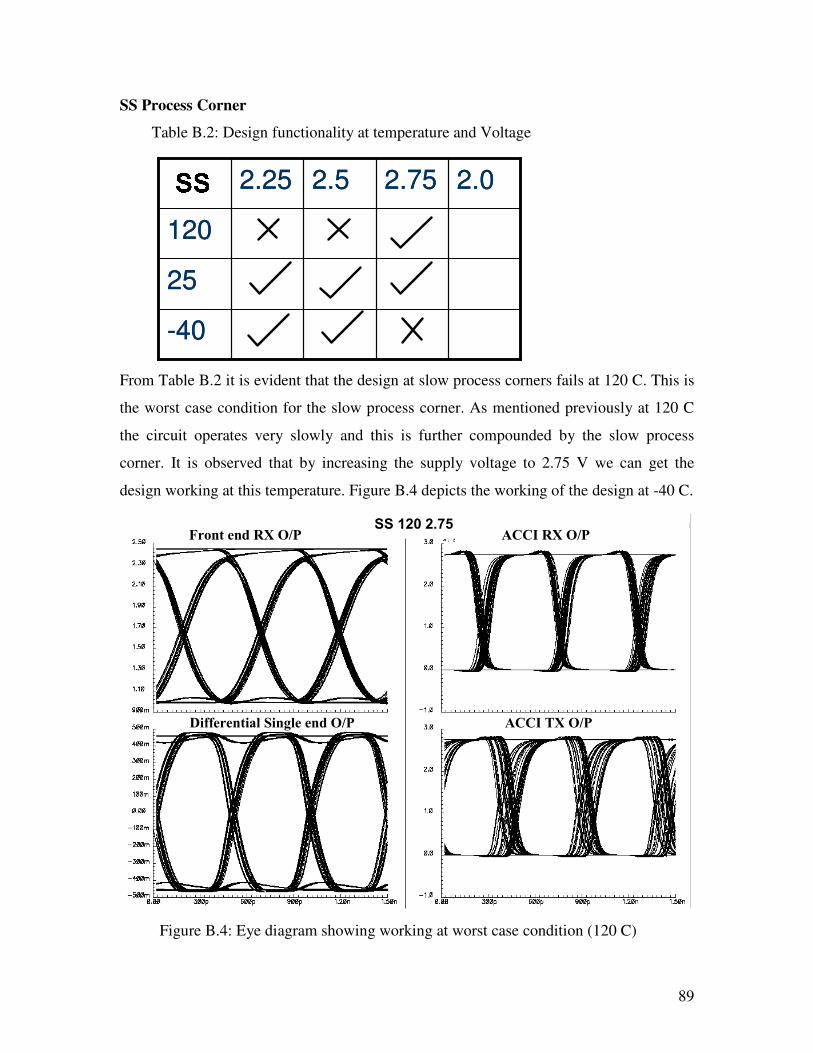
89
SS Process Corner
Table B.2: Design functionality at temperature and Voltage
From Table B.2 it is evident that the design at slow process corners fails at 120 C. This is
the worst case condition for the slow process corner. As mentioned previously at 120 C
the circuit operates very slowly and this is further compounded by the slow process
corner. It is observed that by increasing the supply voltage to 2.75 V we can get the
design working at this temperature. Figure B.4 depicts the working of the design at -40 C.
SS 120 2.75ACCI RX O/PFront end RX O/P
Differential Single end O/P ACCI TX O/P
Figure B.4: Eye diagram showing working at worst case condition (120 C)
-40
25
120
2.02.752.52.25
-40
25
120
2.02.752.52.25

90
As mentioned in the previous section the DC characteristics of the latch is described
using the butterfly plot shown in Figure B.5.
SS 25 C 2.5
NM High = 1.25
NM Low = 1.28
SS 120 C 2.5
NM High = 1.212
NM High = 1.253
Figure B.5: Butterfly plot at 25 C and 120 C for Cross coupled latch

91
FF Process Corner
Table B.3: Design functionality at temperature and Voltage
The worst case temperature for the Fast process corner is -40 C. It is clear that the design
does not function at -40 C. The supply voltage is reduced to 1.6 V to get the design
working at -40C. By reducing the supply voltage the circuit is made to operate at a much
lower speed. This in turn regulates the rise and fall times of the outputs associated with
the inverter. Figure B.6 shows the functionality of the design at -40 C.
FF--40 C 1.6 V
Figure B.6: Eye diagram showing working at worst case condition (-40 C)
-40
25
120
1.62.02.752.502.25
-40
25
120
1.62.02.752.502.25
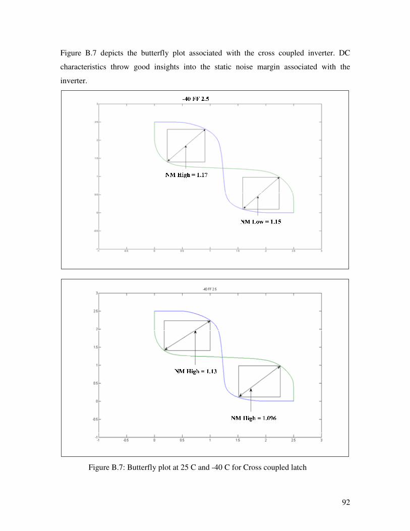
92
Figure B.7 depicts the butterfly plot associated with the cross coupled inverter. DC
characteristics throw good insights into the static noise margin associated with the
inverter.
Figure B.7: Butterfly plot at 25 C and -40 C for Cross coupled latch