bl1400 - digi internationalftp1.digi.com/support/documentation/0190017_02.pdf · bl1400 table of...
TRANSCRIPT
BL1400C-Programmable Controller
Users ManualRevision 2
Z-World BL1400
Users Manual Part Number 019-0017-02Revision 2 021-0026-02 Printed in U.S.A.Last revised by RPB/TI on September 21, 1998
Copyright
© 1998 Z-World All rights reserved.
Z-World reserves the right to make changes and improvements to itsproducts without providing notice.
Trademarks Dynamic C® is a registered trademark of Z-World PLCBus is a trademark of Z-World Windows® is a registered trademark of Microsoft Corporation. Hayes Smart Modem is a trademark of Hayes Microcomputer Products, Inc.
Notice to UsersWhen a system failure may cause serious consequences, protecting life andproperty against such consequences with a backup system or safety deviceis essential. The buyer agrees that protection against consequencesresulting from system failure is the buyers responsibility.
This device is not approved for life-support or medical systems.
Company Address
Z-World2900 Spafford StreetDavis, California 95616-6800 USA
Telephone:Facsimile:
24-Hour FaxBack:Web Site:
E-Mail:
(530) 757-3737(530) 753-5141(530) 753-0618http://www.z [email protected]
Table of Contents s iiiBL1400
TABLE OF CONTENTS
About This Manual vii
BL1400 Overview 1-1BL1400 Overview.............................................................................. 1-2BL1400 Features ................................................................................ 1-3Developers Kit .................................................................................. 1-4Networking ........................................................................................ 1-4Software Development and Evaluation Tools .................................... 1-5
Getting Started 2-1Initial BL1400 Setup .......................................................................... 2-2Connecting the BL1400 to a Host PC ................................................ 2-2
Via Development Board ................................................................ 2-2Via Flash EPROM ......................................................................... 2-5Via Regular EPROM ..................................................................... 2-7
Running Dynamic C ........................................................................... 2-8Test the Communication Line ....................................................... 2-8Selecting Communications Rate, Port, and Protocol .................... 2-8
Running a Sample Program ............................................................... 2-8Power Options ................................................................................... 2-9
BL1400 Subsystems 3-1Operating Modes ............................................................................... 3-2
Changing Baud Rate on the BL1400 ............................................ 3-2Power Connections ....................................................................... 3-2
Interface Description .......................................................................... 3-3Parallel Input/Output (PIO) Chip ....................................................... 3-4
PIO Operation Modes ................................................................... 3-6Control Register Byte Sequence ................................................... 3-7
Header H2 Signals (RS-232 Port) ...................................................... 3-9Header H3 Signals (PIO Ports) .......................................................... 3-9Serial Communication ...................................................................... 3-10
RS-232 Communication .............................................................. 3-10Receive and Transmit Buffers ................................................... 3-10Echo Option .............................................................................. 3-11CTS/RTS Control ..................................................................... 3-11XMODEM File Transfer .......................................................... 3-11Modem Communication ........................................................... 3-11

iv s Table of Contents BL1400
RS-485 Communication .............................................................. 3-12Developing an RS-485 Network ............................................... 3-12Hardware Connection ............................................................... 3-13
Regulator .......................................................................................... 3-14Supervisor ........................................................................................ 3-14Real-Time Clock (RTC) ................................................................... 3-15555 Timer ......................................................................................... 3-16
Using Thermistors ....................................................................... 3-18Memory ............................................................................................ 3-19Direct Programming of the Serial Ports ........................................... 3-20
Attainable Baud Rates ................................................................. 3-21Z180 Serial Ports ...................................................................... 3-21
Asynchronous Serial Communication Interface ............................... 3-23ASCI Status Registers ................................................................. 3-23ASCI Control Register A ............................................................ 3-25ASCI Control Register B ............................................................ 3-26
SS (Source/Speed Select) ......................................................... 3-26DR (Divide Ratio) .................................................................... 3-26PEO (Parity Even/Odd) ............................................................ 3-26CTS/PS (Clear to Send/Prescaler) .......................................... 3-26MP (Multiprocessor Mode) ...................................................... 3-27MPBT (Multiprocessor Bit Transmit) ...................................... 3-27
Software Reference 4-1Software Development Options ......................................................... 4-2
Dynamic C Development Software ............................................... 4-2Dynamic C Manuals ...................................................................... 4-2
Programmable Input/Output .............................................................. 4-3PIO Ports A and B ......................................................................... 4-3
Shadow Registers ........................................................................ 4-3Function Prototypes .................................................................... 4-4
Real-Time Clock Integrated Circuit ................................................... 4-5Global Time and Date Structure .................................................... 4-5
555 Timer ........................................................................................... 4-6Flash EPROM .................................................................................... 4-7Serial Communication Software ........................................................ 4-8
Interrupt Handling for Z180 Port 0 ............................................... 4-8RS-232 Software Support ........................................................... 4-9
XMODEM Commands ............................................................... 4-11Miscellaneous Functions .......................................................... 4-12
Master-Slave Networking ........................................................... 4-14Miscellaneous Functions .......................................................... 4-15

Table of Contents s vBL1400
Support Libraries and Sample Programs ......................................... 4-16Sample Programs ........................................................................ 4-16
Appendix A: Troubleshooting A-1Out of the Box....................................................................................A-2Dynamic C Will Not Start ..................................................................A-2Dynamic C Loses Serial Link ............................................................A-3BL1400 Resets Repeatedly ................................................................A-3Input/Output Problems .......................................................................A-3Power-Supply Problems .....................................................................A-3Common Programming Errors ...........................................................A-4
Appendix B: Specifications B-1Electrical and Mechanical Specifications .......................................... B-2
BL1400 ......................................................................................... B-2Development Board ...................................................................... B-4Prototyping Board ......................................................................... B-5Base Plate ...................................................................................... B-6
Connectors ......................................................................................... B-7Temperature ....................................................................................... B-7Power ................................................................................................. B-7Headers and Jumpers ......................................................................... B-8
BL1400 ......................................................................................... B-8Development Board ...................................................................... B-9
Appendix C: Power Management C-1Direct Current Input ........................................................................... C-2Power Regulator ................................................................................ C-2
Maximum Power Dissipation ........................................................ C-2Heat Dissipation with the BL1400 Base Plate .............................. C-3Heat Dissipation without the Base Plate ....................................... C-4
Appendix D: Prototyping Board D-1Prototyping Board ..............................................................................D-2
Installing the Prototyping Board ...................................................D-4Sample Circuits ..................................................................................D-5
LEDs .............................................................................................D-5Switches ........................................................................................D-5Jumpers .........................................................................................D-5Buzzer ...........................................................................................D-6RC Filter ........................................................................................D-6Thermistor .....................................................................................D-6

vi s Table of Contents BL1400
Appendix E: PLCBus E-1PLCBus Overview ............................................................................. E-2Allocation of Devices on the Bus ...................................................... E-6
4-Bit Devices ................................................................................ E-68-Bit Devices ................................................................................ E-7
Expansion Bus Software .................................................................... E-7
Appendix F: Simulated PLCBus Connection F-1PIO Port Connections ........................................................................ F-2
Expansion Boards ......................................................................... F-2Liquid Crystal Displays and Keypads ........................................... F-3
Software Drivers ................................................................................ F-5Using Expansion Boards with PIO Port A .................................... F-5Using an LCD with PIO Port A ..................................................... F-8Using a Keypad with PIO Ports A and B ...................................... F-9
Appendix G: Input/Output Maps and InterruptVectors G-1
Memory Map .....................................................................................G-2Internal Input/Output Registers .....................................................G-2Other Input/Output Addresses .......................................................G-4
Real-Time Clock (RTC) Registers .....................................................G-4Interrupt Vectors ................................................................................G-6
Interrupt Priorities .........................................................................G-7
Appendix H: Simulated EEPROM H-1
Index
Schematics
About This Manual s viiBL1400
ABOUT THIS MANUAL
This manual provides instructions for installing, testing, configuring, andinterconnecting Z-Worlds BL1400 series controllers.
The term BL1400 will be used generically throughout this manual whenreferring to any controller in the BL1400 series. Where informationapplies to a specific controller, the model number will be specified. Themodels currently covered by this manual include the BL1400 and theBL1410.
Instructions to get started using Dynamic C software programmingfunctions as well as complete C and Dynamic C references and program-ming resources are referenced when necessary.
AssumptionsAssumptions are made regarding the user's knowledge and experience inthe following areas:
Ability to design and engineer a target system that is controlled by acontroller with relay expansion boards.
Understanding of the basics of operating a software program andediting files under Windows on a PC.
Knowledge of the basics of C programming.
For a full treatment of C, refer to the following texts:The C Programming Language by Kernighan and RitchieC: A Reference Manual by Harbison and Steel
Knowledge of basic Z80 assembly language and architecture.
For documentation from Zilog, refer to the following texts:Z180 MPU User's ManualZ180 Serial Communication ControllersZ80 Microprocessor Family User's Manual
$
$

BL1400viii s About This Manual
AcronymsTable 1 is a list of acronyms that may be used in this manual.
ConventionsTable 2 lists and defines typographical conventions that may be used inthis manual.
Table 2. Typographical Conventions
Example Description
while Courier font (bold) indicates a program, a fragment of aprogram, or a Dynamic C keyword or phrase.
// IN-01… Program comments are written in Courier font, plain face.
Italics Indicates that something should be typed instead of theitalicized words (e.g., in place of filename, type a file’sname).
Edit Sans serif font (bold) signifies a menu or menu selection.
. . . An ellipsis indicates that (1) irrelevant program text isomitted for brevity or that (2) preceding program text maybe repeated indefinitely.
[ ] Brackets in a C function’s definition or program segmentindicate that the enclosed directive is optional.
< > Angle brackets occasionally enclose classes of terms.
a | b | c A vertical bar indicates that a choice should be made fromamong the items listed.
Table 1. Acronyms
Acronym Meaning
EPROM Erasable Programmable Read Only Memory
EEPROM Electronically Erasable Programmable ReadOnly Memory
NMI Nonmaskable Interrupt
PIO Parallel Input / Output Circuit(Individually Programmable Input / Output)
PRT Programmable Reload Timer
RAM Random Access Memory
RTC Real Time Clock
SIB Serial Interface Board
SRAM Static Random Access Memory
UART Universal Asynchronous Receiver Transmitter
About This Manual s ixBL1400
Programming Pseudo Types
For convenience, this manual uses the following pseudo types.
uint means unsigned integer
ulong means unsigned long
These pseudo types are not standard C keywords; therefore, they will notfunction in an application unless first declared with typedef or#define.
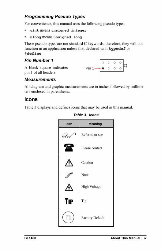
Pin Number 1
A black square indicatespin 1 of all headers.
Measurements
All diagram and graphic measurements are in inches followed by millime-ters enclosed in parenthesis.
IconsTable 3 displays and defines icons that may be used in this manual.
J1Pin 1
Table 3. Icons
Icon Meaning
$ Refer to or see
( Please contact
Caution
! Note
High Voltage
7,3 Tip
Factory Default
FD

BL1400x s About This Manual

BL1400 Overview s 1-1
BL1400 OVERVIEW
Chapter 1 provides an overview and a brief description of the BL1400features and options.

BL14001-2 s Overview
BL1400 OverviewThe BL1400 is a compact and powerful programmable controller. Itssmall size, low cost, and versatility make it ideal for a wide range ofembedded control applications. The BL1400 accepts Z-Worlds 4-bitexpansion boards through its PIO ports.
Figure 1-1 illustrates the BL1400 board layout.
Figure 1-1. BL1400 Board Layout
Y1
Z180
U1
(U5)
EPROM
U7
U3
Reg.
PIO
U6
U2
Y2H3
U4 H2
JP1 32K RAM
Supervisor
(H1)
ParallelPorts,
RS-485,RTC,555,
JP2
C1
C14
RP1
U11U10 U9
U8
RTC
555
R1
RS-232
RS-485RS-232
BOTTOM VIEW
TOP VIEW
BL1400 Overview s 1-3
BL1400 Features Z180 microprocessor running at 6.144 MHz.
Zilog PIO with 12 configurable parallel I/O channels.
32K SRAM, surface-mounted.
EPROM socket for up to 512K EPROM or 256K flash EPROM. TheBL1400 comes with a 32K EPROM installed; 128K or 256K factory-installed flash EPROM options are available.
DS1232 supervisor with watchdog timer and power-failure reset.
Linear regulator (5 V).
RS-232 serial channel.
RS-485 serial channel.
555 timer, configured as an analog input channel.
DS1302 real-time clock (RTC) with 31-byte scratchpad RAM.
Optional base plate for mounting and additional heat sinking.
Table 1-1 lists the versions of the BL1400 Series that are available.
Table 1-1. BL1400 Series Features
Model Features
BL1400 Standard full-featured model.
BL1410BL1400 without RS-485 channel or real-timeclock. Has two additional PIO channels
BL1470EasyStart™ version of BL1410 with 128Kflash EPROM and base plate.
See the BL1470 Users Manual for further information onthe BL1470 and EasyStart.$Appendix B, Specifications, provides a complete list of theBL1400s specifications.$
BL14001-4 s Overview
Developers KitThe BL1400 developers kit contains the following items.
Manual with schematics
Development board
Prototyping board for BL1400 expansion
Aluminum base plate/heat sink
128K flash EPROM
AC power supply
Programming cable
NetworkingThe BL1400s RS-485 capability allows system developers to build anetwork of controllers with links up to several kilometers apart.
The BL1400 was designed to allow users to build and add their ownpiggyback expansion boards. The developers kit contains a prototypingboard for this purpose.
Refer to Appendix D, The Prototyping Board, for moreinformation.$
A BL1400 system may be extended with Z-Worlds standard 4-bit PLCBusexpansion boards. Software for these purposes, which uses the PIO ports,is included in BL14_15.LIB and is described in Chapter 5, SoftwareReference.
See Appendix E, PLCBus, and Appendix F, SimulatedPLCBus Connection, for more information on usingZ-Worlds expansion boards with the BL1400.
$

BL1400 Overview s 1-5
Software Development and Evaluation ToolsDynamic C, Z-Worlds Windows-based real-time C language developmentsystem, is used to develop software for the BL1400. Dynamic C is anintegrated editor-compiler-debugger that runs under Windows on IBM-compatible PCs.
As a program compiles, it is downloaded directly to the BL1400, which isconnected to one of the COM ports on the host PC. Serial communicationis normally at 19,200 bps, but may be as high as 57,600 bps. The control-ler normally remains connected to the PC while a program is undergoingdevelopment. Once program development is complete, the completedprogram may be compiled for EPROM. An EPROM can be burned in aseparate process and installed in the EPROM socket on the BL1400.
On power-up, the Dynamic C BIOS (in the BL1400s EPROM) checks forthe presence of the development board first, then for the presence of flashEPROM. If neither of these is present, Dynamic C reverts to the EPROM.If Dynamic C detects a program in the EPROM, it executes that program.
For ordering information, or for more details about thevarious options and prices, call your Z-World SalesRepresentative at (530) 757-3737.
(
$ Z-Worlds Dynamic C reference manuals provide completesoftware descriptions and programming instructions.

BL14001-6 s Overview

BL1400 Getting Started s 2-1
GETTING STARTED
Chapter 2 provides instructions for connecting the BL1400 to a host PCand running a sample program.
BL14002-2 s Getting Started
Initial BL1400 SetupThe developers kit contains the items necessary for BL1400 software andhardware development. The kit includes the following items.
Development Board for programming the BL1400, with developmentRAM up to 512K
Prototyping Board for prototyping BL1400 expansion circuits andpowering the board during development
Aluminum base plate/heat sink that adds support and allows theBL1400 to dissipate up to 3.5 W at an ambient temperaturesof 50°C
Manual with schematics
128K flash EPROM
AC adapter
Serial programming cable
Miscellaneous small hardware such as 26-pin cable connectors,screws, and standoffs.
Connecting the BL1400 to a Host PCThe BL1400 can be developed in three ways: using the DevelopmentBoard, using flash EPROM, or using regular EPROM. Each method isdescribed below.
On power-up, the Dynamic C BIOS (in the BL1400s EPROM) checks forthe presence of the Development Board first, then for the presence of flashEPROM. If neither is present, Dynamic C searches for a program in theEPROM. If Dynamic C detects a program in the EPROM, it executes thatprogram.
The BL1400 operates either in a program mode or in run mode. Select therun/program mode as described below either through jumpers JP3 and JP4on the Development Board or through header H2 on the Protoyping Board,depending on which development method is being used.
Via Development Board
The Development Board plugs into the EPROM socket of the BL1400.The Development Board has its own RS-232 port, and communicates withthe host PC. It emulates the EPROM normally installed on the BL1400,providing up to 504K of program space in addition to the 32K RAM onthe BL1400 (used as data space).
BL1400 Getting Started s 2-3
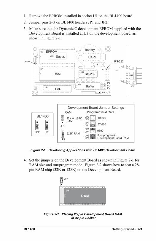
1. Remove the EPROM installed in socket U1 on the BL1400 board.
2. Jumper pins 23 on BL1400 headers JP1 and JP2.
3. Make sure that the Dynamic C development EPROM supplied with theDevelopment Board is installed at U3 on the development board, asshown in Figure 2-1.
U5
U8
U3
Y1
(U1)
U7
U2
U4
JP4JP3JP2
JP5
JP1
H1
EPROM
RAM
PAL
Super. UART
Buffer U6
U5
H2
Battery
RS-232
RS-232
19,200
9600
57,600
JP3JP4
JP3JP4
JP3JP4
JP3JP4
Development Board Jumper Settings
Run program inDevelopment Board RAM
BL1400
JP1JP2
JP1
32K or 128KRAM
JP1
512K RAM
RAM Program/Baud Rate
Figure 2-1. Developing Applications with BL1400 Development Board
4. Set the jumpers on the Development Board as shown in Figure 2-1 forRAM size and run/program mode. Figure 2-2 shows how to seat a 28-pin RAM chip (32K or 128K) on the Development Board.
U5
JP1
RAM
Figure 2-2. Placing 28-pin Development Board RAM in 32-pin Socket

BL14002-4 s Getting Started
5. Plug the Development Board into BL1400 socket U1 and H1, as shownin Figure 2-3. U6 and H2 on the under side of the Development Boardmatch the BL1400 U1 and H1 sockets exactly.
6. Connect the serial cable as shown in Figure 2-4. Connect the 10-pinend to header H1 on the Development Board, taking care to match thearrow on the 10-pin connector to pin 1 on H1. Connect the end withthe DB9 connector to the COM port of your PC.
6. Connect the Prototyping Board to the BL1400 by connecting headerH1 on the underside of the Prototyping Board to H3 on the BL1400 asshown in Figure 2-4. Make sure the Prototyping Board is oriented asshown. Most of the Prototyping Board extends beyond the BL1400.
7. Connect the DC plug from the AC adapter to the DC input jack of thePrototyping Board. Plug in the AC adapter. The BL1400 is now readyfor programming.
Dynamic C is used to create the application, which is then compiled byselecting Compile to File in the Compile menu. Essential library routinesare uploaded from the Dynamic C development EPROM on the Develop-ment Board and are linked to the application being developed. TheDynamic C output is a binary file (or an Intel hex format file) that can beused to burn an EPROM for use in the BL1400.
After the Development Board is removed, the BL1400 will rememberthe last setting established by the Development Board. Be sure to powerthe BL1400 up in run mode (with JP3 and JP4 on the Development Boardconnected as shown in Figure 2-1) before disconnecting the developmentboard. Place the newly burned EPROM in socket U1.
RAM
Z180
PIO
RAM
PAL
EPROMDevelopment B
oard
BL1400
H1
Serialcable toPC
Figure 2-3. Attaching Development Board to BL1400

BL1400 Getting Started s 2-5
Via Flash EPROM
Using the flash EPROM provides up to 256K programming space (in flashEPROM) and 32K in RAM (on the BL1400). The RS-232 port on theBL1400 is used for programming.
1. If necessary, plug a flash EPROM into socket U1 on the BL1400board.
2. Jumper pins 23 on BL1400 header JP1 and pins 12 on BL1400header JP2, which indicates flash EPROM.
3. Connect the Prototyping Board to the BL1400 by connecting headerH1 on the underside of the prototyping board to H3 on the BL1400 asshown in Figure 2-4. Make sure the Prototyping Board is oriented asshown. The Development Board is not used with this developmentmethod. Most of the Prototyping Board extends beyond the BL1400.
Y1
Z180
U7
Reg.PIO
H3
U4
H2
JP1
32K
RA
MC
1
RP
1
JP4JP3JP2
JP5
H1
EPROM
RAM
Development Board
BL1400
Serialcable toPC
PowerJack
SuperCap. Buzzer
Prototyping Board
Figure 2-4. Attaching Prototyping Board to BL1400
BL14002-6 s Getting Started
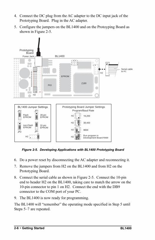
4. Connect the DC plug from the AC adapter to the DC input jack of thePrototyping Board. Plug in the AC adapter.
5. Configure the jumpers on the BL1400 and on the Protoyping Board asshown in Figure 2-5.
19,200
9600
38,400
Prototyping Board Jumper Settings
Run program inDevelopment Board RAM
BL1400 Jumper SettingsProgram/Baud Rate
H21
35
246
H21
35
246
H29
10
H21
35
246
EPROM
PIO
H2
Serial cableto PC
Z180
123
123 1
1
Power Jack
PrototypingBoard
BL1400
H2
H21
35
246
JP2
FlashEPROM
non-FlashEPROM
JP1
28-pinEPROM
32-pinEPROM
JP2 JP1
Figure 2-5. Developing Applications with BL1400 Prototyping Board
6. Do a power reset by disconnecting the AC adapter and reconnecting it.
7. Remove the jumpers from H2 on the BL1400 and from H2 on thePrototyping Board.
8. Connect the serial cable as shown in Figure 2-5. Connect the 10-pinend to header H2 on the BL1400, taking care to match the arrow on the10-pin connector to pin 1 on H2. Connect the end with the DB9connector to the COM port of your PC.
9. The BL1400 is now ready for programming.
The BL1400 will remember the operating mode specified in Step 5 untilSteps 57 are repeated.
BL1400 Getting Started s 2-7
Via Regular EPROM
Using regular EPROM provides up to 32K code and data space, in RAM,on the BL1400. The RS-232 port on the BL1400 is used for programming.
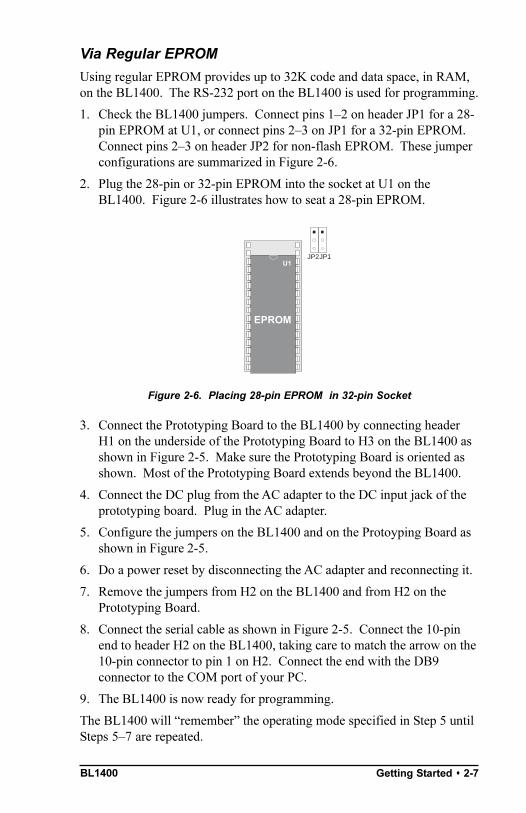
1. Check the BL1400 jumpers. Connect pins 12 on header JP1 for a 28-pin EPROM at U1, or connect pins 23 on JP1 for a 32-pin EPROM.Connect pins 23 on header JP2 for non-flash EPROM. These jumperconfigurations are summarized in Figure 2-6.
2. Plug the 28-pin or 32-pin EPROM into the socket at U1 on theBL1400. Figure 2-6 illustrates how to seat a 28-pin EPROM.
3. Connect the Prototyping Board to the BL1400 by connecting headerH1 on the underside of the Prototyping Board to H3 on the BL1400 asshown in Figure 2-5. Make sure the Prototyping Board is oriented asshown. Most of the Prototyping Board extends beyond the BL1400.
4. Connect the DC plug from the AC adapter to the DC input jack of theprototyping board. Plug in the AC adapter.
5. Configure the jumpers on the BL1400 and on the Protoyping Board asshown in Figure 2-5.
6. Do a power reset by disconnecting the AC adapter and reconnecting it.
7. Remove the jumpers from H2 on the BL1400 and from H2 on thePrototyping Board.
8. Connect the serial cable as shown in Figure 2-5. Connect the 10-pinend to header H2 on the BL1400, taking care to match the arrow on the10-pin connector to pin 1 on H2. Connect the end with the DB9connector to the COM port of your PC.
9. The BL1400 is now ready for programming.
The BL1400 will remember the operating mode specified in Step 5 untilSteps 57 are repeated.
U1
EPROM
JP1JP2
Figure 2-6. Placing 28-pin EPROM in 32-pin Socket
BL14002-8 s Getting Started
Running Dynamic C
Test the Communication Line
Double-click the Dynamic C icon to start the software. Note that the PCattempts to communicate with the BL1400 each time Dynamic C is started.No error messages are displayed once communication is established.
See Appendix A, Troubleshooting, if an error message such asTarget Not Responding or Communication Error appears.
$Once the necessary changes have been made to establishcommunication between the host PC and the BL1400, use theDynamic C shortcut Ctrl Y to reset the controller and initiatecommunication.
!
Selecting Communications Rate, Port, and Protocol
The communication rate, port, and protocol are all selected by choosingSerial Options from Dynamic Cs OPTIONS menu.
The BL1400s factory-default communication rate is 19,200 bps. How-ever, the Dynamic C software may be initialized for a different rate. Tobegin with, use the communications rate of 19,200 bps.
Make sure that the PC serial port used to connect the serial cable (COM1or COM2) is the one selected in the Dynamic C OPTIONS menu. Selectthe 1-stop-bit protocol.
Running a Sample Program1. Open the sample program MGDEMORT.C located in the Dynamic C
SAMPLES\BL14_15 directory.
2. Compile the program by pressing F3 or by choosing Compile from theCompile menu. Dynamic C compiles and downloads the program intothe BL1400s memory. During compilation, Dynamic C rapidlydisplays several messages in the STDIO window. This condition isnormal.
3. Run the program by pressing F9 or by choosing Run from the Runmenu.
4. Press Ctrl Z to stop execution of the program.
5. If needed, press F9 to restart execution of the program.

BL1400 Getting Started s 2-9
Power OptionsDuring software development, the BL1400 draws its power from thePrototyping Board, which is connected to the 9 V DC output of the ACadapter.
After development is complete, connect the 9 V to 12 V power leads fromthe power source to pins 25 (DCIN) and 26 (GND) of header H3 of theBL1400. A 26-pin cable connector in the developers kit may be used tobuild a cable to connect the power source (and other signals).
Customer piggyback expansion boards are normally normally connecteddirectly to header H3 on the BL1400. The expansion boards must havetheir own power connection.

BL14002-10 s Getting Started

BL1400 BL1400 Subsystems s 3-1
BL1400 SUBSYSTEMS
Sections in Chapter 3 discuss the following topics.
Operating Modes
Interface Overview
Parallel Input/Output Chip
H2 Signals
H3 Signals
Serial Communication
Regulator
Supervisor
Real-Time Clock
555 Precision Timer
Memory
BL14003-2 s BL1400 Subsystems
Operating ModesThe BL1400 operates either in a program mode or in run mode. Select therun/program mode either through jumpers JP3 and JP4 on the Develop-ment Board, or through header H2 on the Protoyping Board and header H2on the BL1400, depending on which development method is being used.The BL1400 will remember the latest settings after the DevelopmentBoard or the Prototyping Boards have been removed.
When in run mode, the BL1400 will look for and then execute the programin EPROM upon power-up.
Changing Baud Rate on the BL1400
The baud rate may be changed by connecting the appropriate pins on theDevelopment Board or the Prototyping Board, depending on whichdevelopment method is being used. The baud rate may be changed afterthe application has been developed. The BL1400 will remember the latestsettings after the Development Board or the Prototyping Board has beenremoved.
Power Connections
After development is complete, connect the 9 V to 12 V power leads fromthe power source to pins 25 (DCIN) and 26 (GND) of header H3 of theBL1400. A 26-pin cable connector in the developers kit may be used tobuild a cable to connect the power source (and other signals).
See Chapter 2, Getting Started, for complete details onconfiguring the BL1400 for programming or standaloneoperation.
$
BL1400 BL1400 Subsystems s 3-3
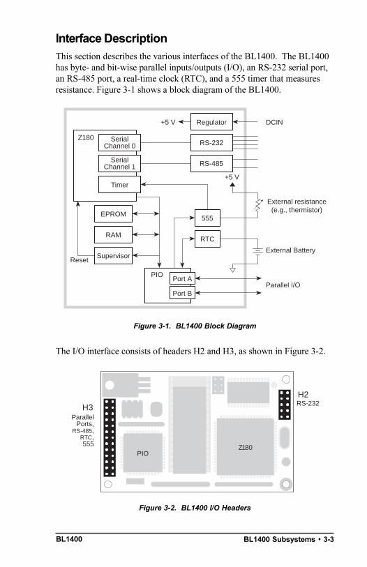
Figure 3-2. BL1400 I/O Headers
Z180PIO
H3
H2
ParallelPorts,
RS-485,RTC,555
RS-232
The I/O interface consists of headers H2 and H3, as shown in Figure 3-2.
Figure 3-1. BL1400 Block Diagram
Z180
Regulator DCIN
SerialChannel 0
Timer
SerialChannel 1
555
RTC
EPROM
RAM
Supervisor
PIOPort A
Port B
Reset
Parallel I/O
External Battery
External resistance(e.g., thermistor)
+5 V
+5 V
RS-232
RS-485
Interface DescriptionThis section describes the various interfaces of the BL1400. The BL1400has byte- and bit-wise parallel inputs/outputs (I/O), an RS-232 serial port,an RS-485 port, a real-time clock (RTC), and a 555 timer that measuresresistance. Figure 3-1 shows a block diagram of the BL1400.
BL14003-4 s BL1400 Subsystems
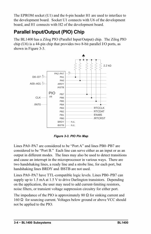
The EPROM socket (U1) and the 6-pin header H1 are used to interface tothe development board. Socket U1 connects with U6 of the developmentboard, and H1 connects with H2 of the development board.
Parallel Input/Output (PIO) ChipThe BL1400 has a Zilog PIO (Parallel Input/Output) chip. The Zilog PIOchip (U6) is a 44-pin chip that provides two 8-bit parallel I/O ports, asshown in Figure 3-3.
Figure 3-3. PIO Pin Map
/INT0
CLK
2
PB5
PA2–PA7
PIOU6
6
PB0
PB1
PB2
PB3
PB4
PB6
PB7
PA1
PA0
RTCDATRTCCLK
/RTCRSTEN485
ARDY
/ASTB
BRDY
/BSTB
n.c.n.c.
D0–D7 8
A00–A01
2.2 kΩ
Lines PA0PA7 are considered to be Port A and lines PB0PB7 areconsidered to be Port B. Each line can serve either as an input or as anoutput in different modes. The lines may also be used to detect transitionsand cause an interrupt in the microprocessor in various ways. There aretwo handshaking lines, a ready line and a strobe line, for each port, buthandshaking lines BRDY and /BSTB are not used.
Lines PA0PA7 have TTL-compatible logic levels. Lines PB0PB7 cansupply up to 1.5 mA at 1.5 V to drive Darlington transistors. Dependingon the application, the user may need to add current-limiting resistors,noise filters, or transient voltage suppression circuitry for either port.
The impedance of the PIO is approximately 80 Ω for sinking current and160 Ω for sourcing current. Voltages below ground or above VCC shouldnot be applied to the PIO.
BL1400 BL1400 Subsystems s 3-5
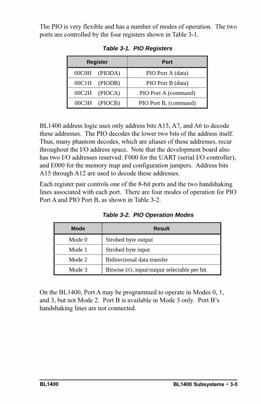
The PIO is very flexible and has a number of modes of operation. The twoports are controlled by the four registers shown in Table 3-1.
Table 3-1. PIO Registers
Register Port
00C0H (PIODA) PIO Port A (data)
00C1H (PIODB) PIO Port B (data)
00C2H (PIOCA) PIO Port A (command)
00C3H (PIOCB) PIO Port B, (command)
BL1400 address logic uses only address bits A15, A7, and A6 to decodethese addresses. The PIO decodes the lower two bits of the address itself.Thus, many phantom decodes, which are aliases of these addresses, recurthroughout the I/O address space. Note that the development board alsohas two I/O addresses reserved: F000 for the UART (serial I/O controller),and E000 for the memory map and configuration jumpers. Address bitsA15 through A12 are used to decode these addresses.
Each register pair controls one of the 8-bit ports and the two handshakinglines associated with each port. There are four modes of operation for PIOPort A and PIO Port B, as shown in Table 3-2.
Table 3-2. PIO Operation Modes
Mode Result
Mode 0 Strobed byte output
Mode 1 Strobed byte input
Mode 2 Bidirectional data transfer
Mode 3 Bitwise I/O, input/output selectable per bit
On the BL1400, Port A may be programmed to operate in Modes 0, 1,and 3, but not Mode 2. Port B is available in Mode 3 only. Port Bshandshaking lines are not connected.

BL14003-6 s BL1400 Subsystems
Four of port Bs lines are preassigned, as shown in Table 3-3 (see alsoFigure 3-3).
Table 3-3. Preasssigned PIO Lines
PIO Port Pin Signal Pin Function
PB3 RTCCLK DS1302 RTC serial clock
PB2 RTCDAT DS1302 RTC serial data
PB1 EN485 RS485 transmit enable
PB0 /RTCRST 555 trigger and DS1302 RTC reset
PB3 and PB2 can be used as two additional parallel I/O if the real-timeclock is not being used.
The PIO uses /INT0 of the Z180. The PIO can be programmed to inter-rupt the Z180 upon the transfer of each byte of data during handshakemode, or upon the change of state of individual bits during bit I/O mode.
Refer to Zilogs Z80180/Z180 MPU Users Manual forcomplete details.$
PIO Operation Modes
Mode 0 (Strobed Byte Output)
When the microprocessor stores a byte in a ports data register, the eightassociated output lines change their level according to how each bit is set:to high for a 1 and low for a 0. The ready handshake line goes high.When an external device pulses the strobe line (low), the ready line isreset. If interrupts are enabled for the port, a PIO interrupt is requested.This allows for interrupt-driven parallel output.
Mode 1 (Strobed Byte Input)
The PIO latches eight bits into a register upon the strobe signal from anexternal device. The strobe signal also causes the ready line to go low. Aninterrupt is then requested. After the microprocessor reads the register, theready line is raised to indicate that the port is ready for another byte.
Mode 2 (Bidirectional Data Transfer)
Mode 2 is not available on the BL1400.
Mode 3 (Bitwise I/O)
This is a general-purpose I/O mode. Each bit can be individually specifiedas input or output. In this mode, the input lines can also serve as interruptrequest lines. Either transition to high or transition to low can be specifiedfor the interrupt request. Interrupts for specific input lines are controlledwith a mask and by specifying an AND or an OR function for the maskedlines. Interrupts on PIO ports are edge-triggered.

BL1400 BL1400 Subsystems s 3-7
Control Register Byte Sequence
To set up a port for I/O, first write a sequence of bytes to its controlregister. Then read, or write, its data register to transfer data.
The control register byte sequence is shown below.
mode control wordI/O register control word (only if mode 3)interrupt vector wordinterrupt control wordmask control wordinterrupt disable word
The mode control word specifies the mode for the port.
0 0 = Mode 00 1 = Mode 11 0 = Mode 21 1 = Mode 3
Identifies this asmode control word
1D7 D6 X X 1 1 1
The I/O register control word must immediately follow the mode controlword, but only in Mode 3 (bitwise I/O). This byte specifies which bits areinputs and which bits are outputs for bitwise I/O.
0 – bit is output1 – bit is input
D0D7 D6 D5 D4 D3 D2 D1
The interrupt vector word specifies the interrupt vector for the particularPIO channel.
interrupt vectorIdentifies this asinterrupt vector word
0D7 D6 D5 D4 D3 D2 D1
The vectors for the PIO ports are as follows.
0x12 (PIOA_VEC) PIO Port A0x14 (PIOB_VEC) PIO Port B
BL14003-8 s BL1400 Subsystems
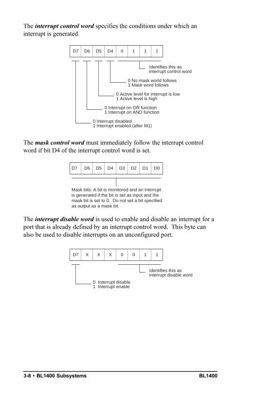
The interrupt control word specifies the conditions under which aninterrupt is generated.
0 No mask world follows1 Mask word follows
Identifies this asinterrupt control word
1D7 D6 D5 D4 0 1 1
0 Active level for interrupt is low1 Active level is high
0 Interrupt on OR function1 Interrupt on AND function
0 Interrupt disabled1 Interrupt enabled (after M1)
The mask control word must immediately follow the interrupt controlword if bit D4 of the interrupt control word is set.
Mask bits: A bit is monitored and an interruptis generated if the bit is set as input and themask bit is set to 0. Do not set a bit specifiedas output as a mask bit.
D0D7 D6 D5 D4 D3 D2 D1
The interrupt disable word is used to enable and disable an interrupt for aport that is already defined by an interrupt control word. This byte canalso be used to disable interrupts on an unconfigured port.
Identifies this asinterrupt disable word
1D7 X X X 0 0 1
0 Interrupt disable1 Interrupt enable
BL1400 BL1400 Subsystems s 3-9
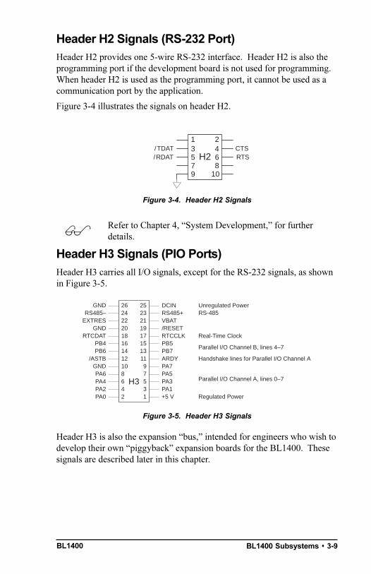
Header H2 Signals (RS-232 Port)Header H2 provides one 5-wire RS-232 interface. Header H2 is also theprogramming port if the development board is not used for programming.When header H2 is used as the programming port, it cannot be used as acommunication port by the application.
Figure 3-4 illustrates the signals on header H2.
Figure 3-5. Header H3 Signals
Regulated Power
H3
GND
PA6
RS485–EXTRES
GND
PB4PB6
/ASTBGND
2624222018161412108
252321191715131197
DCIN
PA5
RS485+VBAT/RESETRTCCLKPB5PB7ARDYPA7
PA4 6 5 PA3PA2 4 3 PA1PA0 2 1
RTCDAT
Unregulated Power
Real-Time Clock
Parallel I/O Channel B, lines 4–7
Handshake lines for Parallel I/O Channel A
Parallel I/O Channel A, lines 0–7
RS-485
+5 V
Figure 3-4. Header H2 Signals
13579
2468
H2
10
CTSRTS
/TDAT/RDAT
Refer to Chapter 4, System Development, for furtherdetails.$
Header H3 Signals (PIO Ports)Header H3 carries all I/O signals, except for the RS-232 signals, as shownin Figure 3-5.
Header H3 is also the expansion bus, intended for engineers who wish todevelop their own piggyback expansion boards for the BL1400. Thesesignals are described later in this chapter.
BL14003-10 s BL1400 Subsystems
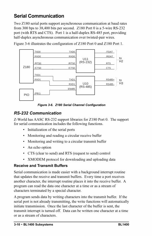
Serial CommunicationTwo Z180 serial ports support asynchronous communication at baud ratesfrom 300 bps to 38,400 bits per second. Z180 Port 0 is a 5-wire RS-232port (with RTS and CTS). Port 1 is a half-duplex RS-485 port, providinghalf-duplex asynchronous communication over twisted-pair wires.
Figure 3-6 illustrates the configuration of Z180 Port 0 and Z180 Port 1.
Figure 3-6. Z180 Serial Channel Configuration
TXD1
/CTS0
RXD1
TXD1
RXD0
TXD0
Z180 CTS
RTS
/RDAT
/TDAT
/CTS0
/RTS0
RXD0
TXD0
/RTS0
RS485–
RS485+
RXD1
toH2
toH3
EN485
PIO (PB1)
U11(RS-232)
U10(RS-485)
RS-232 Communication
Z-World has AASC RS-232 support libraries for Z180 Port 0. The supportfor serial communication includes the following functions.
Initialization of the serial ports
Monitoring and reading a circular receive buffer
Monitoring and writing to a circular transmit buffer
An echo option
CTS (clear to send) and RTS (request to send) control
XMODEM protocol for downloading and uploading data
Receive and Transmit Buffers
Serial communication is made easier with a background interrupt routinethat updates the receive and transmit buffers. Every time a port receivesanother character, the interrupt routine places it into the receive buffer. Aprogram can read the data one character at a time or as a stream ofcharacters terminated by a special character.
A program sends data by writing characters into the transmit buffer. If theserial port is not already transmitting, the write functions will automaticallyinitiate transmission. Once the last character of the buffer is sent, thetransmit interrupt is turned off. Data can be written one character at a timeor as a stream of characters.

BL1400 BL1400 Subsystems s 3-11
Echo Option
If the echo option is turned on with Dinit_z0 during initialization of theserial port, any character received is automatically echoed back (transmit-ted out). This feature is ideal for use with a dumb terminal and also forchecking the characters received.
CTS/RTS Control
Z180 Port 0 is constrained by hardware to have the CTS (clear to send)pulled low by the RS-232 device to which it is talking.
If the CTS/RTS option is chosen, the support software will pull the RTS(request to send) line high when the receive buffer has reached 80% of itscapacity. Thus, the transmitting device (if its CTS is enabled) will stoptransmitting. The RTS line is pulled low again when the receive buffer hasgone below 20% of its capacity.
If the device with which the BL1400 is communicating does not supportCTS and RTS, the CTS and RTS lines on the BL1400 side must be tiedtogether to make communication possible.
The CTS line must be pulled up when not in use.
XMODEM File Transfer
The BL1400 supports the XMODEM protocol for downloading anduploading data. Currently, the library supports downloading an array ofdata whose size is a multiple of 128 bytes.
Uploaded data are written to a specified area in RAM. The targeted areafor writing should not conflict with the current resident program or data.
Character echo is automatically suspended during XMODEM transfer.
Modem Communication
Modems and telephone lines enable RS-232 communication across greatdistances. If the modem option is chosen, character streams that are readfrom the receive buffer are automatically scanned for modem commands.When a modem command is found, the software takes appropriate action.Normally, the communication package would be in COMMAND modewhile waiting for valid modem commands or messages. Once a link isestablished, the communication is in DATA mode (regular RS-232).However, the software continues to monitor the modem for a NO_CARRIERmessage.
BL14003-12 s BL1400 Subsystems
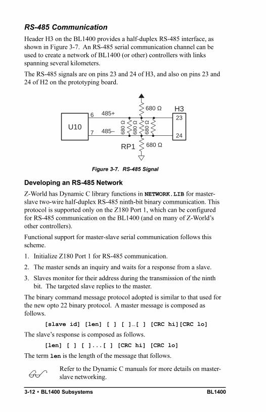
RS-485 Communication
Header H3 on the BL1400 provides a half-duplex RS-485 interface, asshown in Figure 3-7. An RS-485 serial communication channel can beused to create a network of BL1400 (or other) controllers with linksspanning several kilometers.
The RS-485 signals are on pins 23 and 24 of H3, and also on pins 23 and24 of H2 on the prototyping board.
Developing an RS-485 Network
Z-World has Dynamic C library functions in NETWORK.LIB for master-slave two-wire half-duplex RS-485 ninth-bit binary communication. Thisprotocol is supported only on the Z180 Port 1, which can be configuredfor RS-485 communication on the BL1400 (and on many of Z-Worldsother controllers).
Functional support for master-slave serial communication follows thisscheme.
1. Initialize Z180 Port 1 for RS-485 communication.
2. The master sends an inquiry and waits for a response from a slave.
3. Slaves monitor for their address during the transmission of the ninthbit. The targeted slave replies to the master.
The binary command message protocol adopted is similar to that used forthe new opto 22 binary protocol. A master message is composed asfollows.
[slave id] [len] [ ] [ ][ ] [CRC hi][CRC lo]
The slaves response is composed as follows.
[len] [ ] [ ]...[ ] [CRC hi] [CRC lo]
The term len is the length of the message that follows.
Figure 3-7. RS-485 Signal
23
24
H3
U10
485+
485–
6
7
RP1
680 Ω
680 Ω
680
Ω
680
Ω
680
Ω
Refer to the Dynamic C manuals for more details on master-slave networking.$

BL1400 BL1400 Subsystems s 3-13
Hardware Connection
Figure 3-8 shows the connections for a two-wire RS-485 network. On allnetworked controllers, connect RS-485+ to RS-485+ and RS-485- toRS-485- using single twisted pair wires (nonstranded, tinned).
BL1400
BL1400
Enable terminationresistors on themaster controllerand end controlleronly
H3
BL1400
H3
H3
Figure 3-8. BL1400 Multidrop RS-485 Network
Any one of Z-Worlds controllers can be a master or a slave. While therecan only be one master, there can be up to 255 slaves. The master shouldhave a board identification address of 0. Slaves should each have theirown distinct identification address from 1 to 255.
Termination and bias resistors are required in a multidrop network tominimize reflections (echoing), and to keep the network line active in anidle state. Typically, 120 Ω termination resistors are installed across themaster node and across the physical end node of an RS-485 network.
Contact Z-World Technical Support at (530) 757-3737for assistance with large-scale network design.(

BL14003-14 s BL1400 Subsystems
Figure 3-9. Reset Circuit
19
20
H3
ExternalReset
/RESETZ180
U7
/RESET8
DS1232
U2
7
6
HITWD
2.2 kΩ
0.47 µF
22
*100 Ω–200 Ω
* Add resistor and small capacitoras shown if debouncing is needed
*C
See Appendix C, Power Management, for more informa-tion.$
RegulatorAn on-board +5 V linear regulator (U3) accepts 9 V to 12 V DC. This isDCIN. The regulator has some excess capacity to power expansion boardsor external loads.
The maximum power dissipation is 1.0 W at 70°C without additional heatsinking. The BL1400 itself draws 120 mA, dissipating about 0.85 W with12 V input. Additional heat sinking can be obtained by mounting theBL1400 on the optional aluminum base plate, using aluminum standoffs.
SupervisorThe DS1232 supervisor (U2) provides a watchdog timer that guardsagainst system or software faults by resetting the Z180 microprocessor ifthe software does not hit the timer at least every 1.2 seconds.by making acall to hitwd. The supervisor also provides the reset signal for themicroprocessor and the rest of the system on power-up or when VCC(normally +5 V) falls below 4.62 V.
The negative-going reset signal (/RESET) (shown in Figure 3-8) is activefor at least 250 ms after VCC reaches 4.62 V. /RESET is an open-drainsignal, pulled up by a 2.2 kΩ resistor
An external reset switch can be added as shown in Figure 3-9. A smallcapacitor can also be added if debouncing is needed.
BL1400 BL1400 Subsystems s 3-15
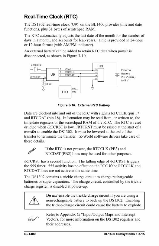
Data are clocked into and out of the RTC with signals RTCCLK (pin 17)and RTCDAT (pin 18). Information may be read from, or written to, thetime/date registers or the scratchpad RAM of the RTC. The RTC is resetor idled when /RTCRST is low. /RTCRST must be raised at the start of atransfer to enable the DS1302. It must be lowered at the end of thetransfer to terminate the transfer. Z-World software drivers take care ofthese details.
If the RTC is not present, the RTCCLK (PB3) andRTCDAT (PB2) lines may be used for other purposes.!
/RTCRST has a second function. The falling edge of /RTCRST triggersthe 555 timer. 555 activity has no effect on the RTC if the RTCCLK andRTCDAT lines are not active at the same time.
The DS1302 contains a trickle charge circuit to charge rechargeablebatteries or super capacitors. The charge circuit, controlled by the tricklecharge register, is disabled at power-up.
Refer to Appendix G, Input/Output Maps and InterruptVectors, for more information on the DS1302 registers andtheir addresses.
$
Real-Time Clock (RTC)The DS1302 real-time clock (U9) on the BL1400 provides time and datefunctions, plus 31 bytes of scratchpad RAM.
The RTC automatically adjusts the last date of the month for the number ofdays in a month, and accounts for leap years. Time is provided in 24-houror 12-hour format (with AM/PM indicator).
An external battery can be added to retain RTC data when power isdisconnected, as shown in Figure 3-10.
Figure 3-10. External RTC Battery
RTCDATRTCCLK
21H3
U9
VBAT8
7
32768 Hz
/RTCRST6
17
18
205
ExternalBattery2.5 V (min.)to 5 V
PIOPB2
PB3
10 kΩ
Do not enable the trickle charge circuit if you are using anonrechargeable battery to back up the DS1302. Enablingthe trickle-charge circuit could cause the battery to explode.
BL14003-16 s BL1400 Subsystems
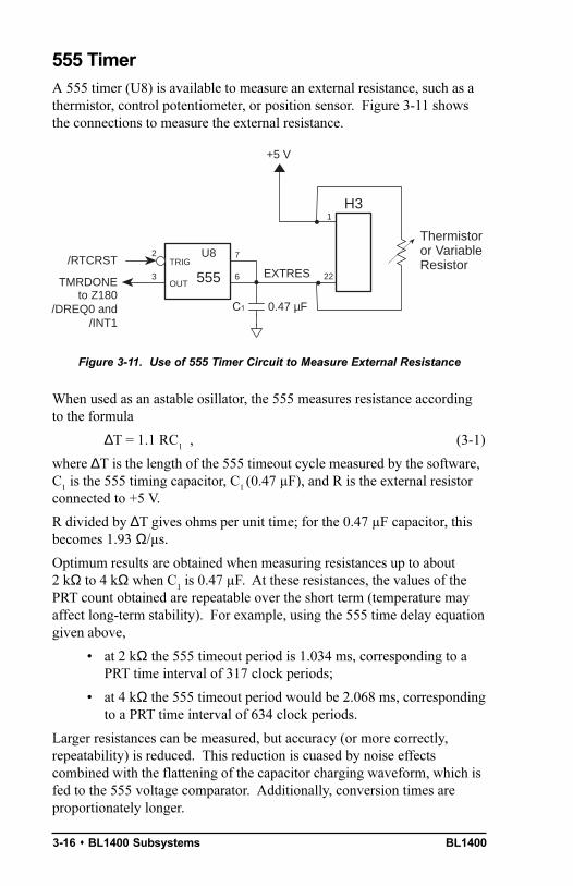
555 TimerA 555 timer (U8) is available to measure an external resistance, such as athermistor, control potentiometer, or position sensor. Figure 3-11 showsthe connections to measure the external resistance.
Figure 3-11. Use of 555 Timer Circuit to Measure External Resistance
1
22
H3
Thermistoror VariableResistor
555
U82
3
TRIG
OUT
7
6
/RTCRST
TMRDONEEXTRES
to Z180/DREQ0 and
/INT10.47 µFC1
+5 V
When used as an astable osillator, the 555 measures resistance accordingto the formula
∆T = 1.1 RC1 , (3-1)
where ∆T is the length of the 555 timeout cycle measured by the software,C
1 is the 555 timing capacitor, C
1 (0.47 µF), and R is the external resistor
connected to +5 V.
R divided by ∆T gives ohms per unit time; for the 0.47 µF capacitor, thisbecomes 1.93 Ω/µs.
Optimum results are obtained when measuring resistances up to about2 kΩ to 4 kΩ when C
1 is 0.47 µF. At these resistances, the values of the
PRT count obtained are repeatable over the short term (temperature mayaffect long-term stability). For example, using the 555 time delay equationgiven above,
at 2 kΩ the 555 timeout period is 1.034 ms, corresponding to aPRT time interval of 317 clock periods;
at 4 kΩ the 555 timeout period would be 2.068 ms, correspondingto a PRT time interval of 634 clock periods.
Larger resistances can be measured, but accuracy (or more correctly,repeatability) is reduced. This reduction is cuased by noise effectscombined with the flattening of the capacitor charging waveform, which isfed to the 555 voltage comparator. Additionally, conversion times areproportionately longer.
BL1400 BL1400 Subsystems s 3-17
The initial accuracies and temperature stability of the primary componentslisted below contribute to the overall accuracy of 555 resistance measure-ments.
The Z180 crystal. The initial accuracy of the crystal is 0.005%, or 50parts per million.
The 555 timer. The data sheet for the Phillips NE555D specifies atemperature stability of 0.005% per degree Celcius, or 50 parts permillion, referenced to 25°C. The initial deviation of the NE555D isspecified as 1% typical, 3% maximum. This represents a temperaturestability of 0.225% over the operating temperature range of theBL1400 (0°C to 70°C).
The onboard timing capacitor C1. For C
1, the value is 10%. Timing
capacitor C1 has an X7R temperature coefficient that results in a
temperature stability of approximately 2% to 3%, varying somewhatwith the manufacturer, over the operating temperature range of theBL1400.
The external resistor. The user must determine the initial accuracy ofthe external resistor.
When measuring temperature with a thermistor, the temperature coefficientof the thermistor, discussed in the next section, is the primary consider-ation. When measuring an external variable resistance, be aware of itstemperature coefficient and the effect the temperature coefficient has onthe overall accuracy of the measurement.
For maximum accuracy, connect the external resistance to the +5 V supplyof the BL1400, as shown in Figure 3-10. Do not return the externalresistor to another power supply in the system.
Phillips and other manufacturers have published severaluseful application notes that describe in detail how to use the555 effectively. These notes include important precautionsas well as suggestions for ensuring reliable results.
$
$ See Chapter 5, Software Reference, for functions thatread the 555.

BL14003-18 s BL1400 Subsystems
Using Thermistors
Negative temperature coefficient (NTC) thermistors are frequently used asinexpensive and reasonably accurate temperature sensors. Units withinitial accuracies of 1% are available.
This section presents a brief summary of the use of thermistors as tempera-ture sensors.
Refer to a specific manufacturers literature for additionaldetail.$
The resistance of an NTC thermistor varies inversely with temperatureaccording to Equation (3-2).
R = Aeß/T (T in kelvins) (3-2)
Two parameters are typically specified for a thermistor: its resistance at25°C and its temperature coefficient α (alpha), expressed as the percentchange of resistance per degree Celcius at 25°C. ß (beta) in the tempera-ture equation is computed from α, or is sometimes given by the manufac-turer:
ß = T2α (T = 25°C, or 298.15 K) .
α (alpha) is defined as 1/R × dR/dT, and equals β/T2 fromthe resistance equation.!
.)]907.3(R[ln
3911
A)lnR(lnKelvins)(in T
−−=
−=
β
Once β is known, A can be computed from the resistance at 25°C.
For example: assume a thermistor with α = 4.40% per degree Celcius andR, at 25°C, of 10 kΩ. Then,
ß = (298.15 K × 298.15 K) × (0.044 K-1)
= 3911 K .
Since the resistance at 25°C is 10 kΩ,
10,000 Ω = Ae(3911 K/298.15 K)
= A × 497,600 .
Therefore,
A = 10,000 Ω/497,600 = 0.0200 Ω , and
ln A = -3.907 .
Using the resistance equation and expressing T as a function of R,
BL1400 BL1400 Subsystems s 3-19
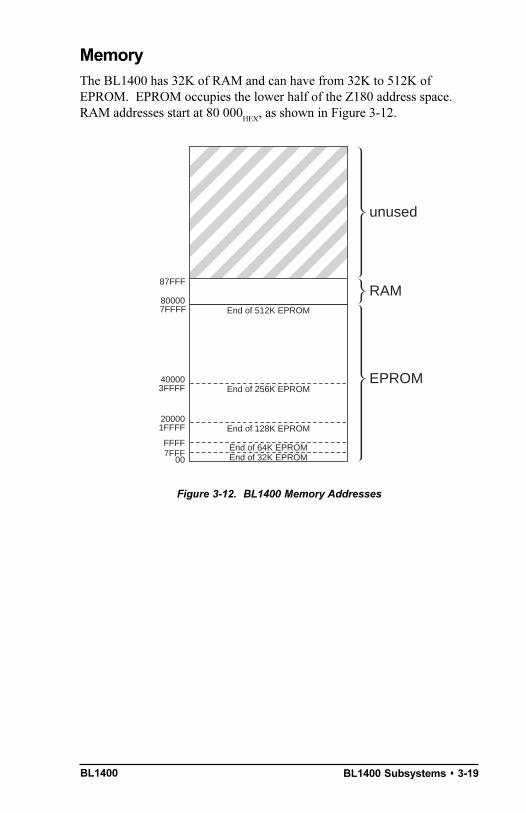
Figure 3-12. BL1400 Memory Addresses
End of 32K EPROMEnd of 64K EPROM
RAM
EPROM
7FFFF80000
87FFF
3FFFF
1FFFF
7FFF
40000
20000
00
FFFF
End of 128K EPROM
End of 256K EPROM
End of 512K EPROM
unused
MemoryThe BL1400 has 32K of RAM and can have from 32K to 512K ofEPROM. EPROM occupies the lower half of the Z180 address space.RAM addresses start at 80 000
HEX, as shown in Figure 3-12.
BL14003-20 s BL1400 Subsystems
Direct Programming of the Serial PortsIf you are planning extensive use of the serial ports, or intend to usesynchronous communication, Z-World recommends that you obtain copiesof the Zilog technical manuals. You will need the Z180 MPU UsersManual and the Z180 Microprocessor Family Users Manual (whichdescribes the CPU and CTC, DMA, PIO and SIO functions). Z-Worldprovides just a few low-level utility functions.
int sysclock()
Returns the clock frequency in multiples of 1200 bps, as read fromRAM. The fixed clock frequency is stored at location 108H at thefactory.
int z180baud( int clock, int baud )
Returns the byte to be stored in CNTLB0 or CNTLB1, consideringonly the bits needed to set the baud rate. The clock and baud rate mustbe supplied in multiples of 1200 Hz. Thus, a 6.144 MHz clock isexpressed by 5120 and 19,200 bps is expressed by 16. The returnvalue is 1 if the value for the baud rate cannot be derived from thegiven clock frequency.
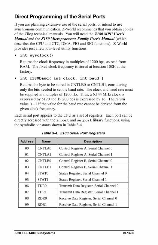
Each serial port appears to the CPU as a set of registers. Each port can bedirectly accessed with the inport and outport library functions, usingthe symbolic constants shown in Table 3-4.
Table 3-4. Z180 Serial Port Registers
Address Name Description
00 CNTLA0 Control Register A, Serial Channel 0
01 CNTLA1 Control Register A, Serial Channel 1
02 CNTLB0 Control Register B, Serial Channel 0
03 CNTLB1 Control Register B, Serial Channel 1
04 STAT0 Status Register, Serial Channel 0
05 STAT1 Status Register, Serial Channel 1
06 TDR0 Transmit Data Register, Serial Channel 0
07 TDR1 Transmit Data Register, Serial Channel 1
08 RDR0 Receive Data Register, Serial Channel 0
09 RDR1 Receive Data Register, Serial Channel 1
BL1400 BL1400 Subsystems s 3-21
For example, use the following code to read and write from Serial Port 0.
char ch;ch = inport( RDR0 );outport( TDR0, ch );
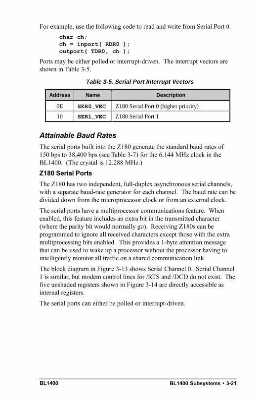
Ports may be either polled or interrupt-driven. The interrupt vectors areshown in Table 3-5.
Table 3-5. Serial Port Interrupt Vectors
Address Name Description
0E SER0_VEC Z180 Serial Port 0 (higher priority)
10 SER1_VEC Z180 Serial Port 1
Attainable Baud Rates
The serial ports built into the Z180 generate the standard baud rates of150 bps to 38,400 bps (see Table 3-7) for the 6.144 MHz clock in theBL1400. (The crystal is 12.288 MHz.)
Z180 Serial Ports
The Z180 has two independent, full-duplex asynchronous serial channels,with a separate baud-rate generator for each channel. The baud rate can bedivided down from the microprocessor clock or from an external clock.
The serial ports have a multiprocessor communications feature. Whenenabled, this feature includes an extra bit in the transmitted character(where the parity bit would normally go). Receiving Z180s can beprogrammed to ignore all received characters except those with the extramultiprocessing bits enabled. This provides a 1-byte attention messagethat can be used to wake up a processor without the processor having tointelligently monitor all traffic on a shared communication link.
The block diagram in Figure 3-13 shows Serial Channel 0. Serial Channel1 is similar, but modem control lines for /RTS and /DCD do not exist. Thefive unshaded registers shown in Figure 3-14 are directly accessible asinternal registers.
The serial ports can either be polled or interrupt-driven.

BL14003-22 s BL1400 Subsystems
A polling driver tests the ready flags (TDRE and RDRF) until a readycondition appears (transmitter data register empty or receiver data registerfull). If an error condition occurs on receive, the routine must clear theerror flags and take appropriate action, if any. If the /CTS line is used forflow control, transmission of data is automatically stopped when /CTSgoes high because the TDRE flag is disabled. This prevents the driverfrom transmitting more characters because it thinks the transmitter is notready. The transmitter will still function with /CTS high, but exercise caresince TDRE is not available to synchronize loading the data register(TDR) properly.
An interrupt-driven driver works as follows. The program enables thereceiver interrupt as long as it wants to receive characters. The transmitterinterrupt is enabled only while characters are waiting in the output buffer.When an interrupt occurs, the interrupt routine must determine the cause:receiver data register full, transmitter data register empty, receiver error, or/DCD0 pin high (channel 0 only). None of these interrupts is edge-triggered. Another interrupt will occur immediately if interrupts are re-enabled without disabling the condition causing the interrupt. The signal/DCD0 is grounded on the BL1400.
Microprocessor Internal Bus
RDR0 TDR0
TSR0RXA0 TXA0
Shift Register OutShift Register In
Baud-RateGenerator
CKA0CNTLA0
STAT0
CNTLB0
/RTS0
/CTS0
/DCD0
RSR0
Figure 3-13. Z180 Serial Channel 0

BL1400 BL1400 Subsystems s 3-23
Asynchronous Serial Communication InterfaceThe Z180 incorporates an asynchronous serial communication interface(ASCI) that supports two independent full-duplex channels.
ASCI Status Registers
A status register for each channel provides information about the state ofeach channel and allows interrupts to be enabled and disabled.
STAT0 (04H)7 6 5 4 3 2 1 0
RDRF OVRN PE FE RIE /DCD0 TDRE TIE
R R R R R / W R R R / W
STAT1 (05H)7 6 5 4 3 2 1 0
RDRF OVRN PE FE RIE CTS1E TDRE TIE
R R R R R / W R R R / W
/DCD0 (Data Carrier Detect)
This bit echoes the state of the /DCD0 input pin for Channel 0. However,when the input to the pin switches from high to low, the data bit switcheslow only after STAT0 has been read. The receiver is held reset as long asthe input pin is held high. This function is not generally useful because aninterrupt is requested as long as /DCD0 is a 1. This forces the programmerto disable the receiver interrupts to avoid endless interrupts. A betterdesign would cause an interrupt only when the state of the pin changes. Inthe BL1400, this pin is tied to ground.
TIE (Transmitter Interrupt Enable)
This bit masks the transmitter interrupt. If set to 1, an interrupt is re-quested whenever TDRE is 1. The interrupt is not edge-triggered. Set thisbit 0 to stop sending. Otherwise, interrupts will be requested continuouslyas soon as the transmitter data register is empty.
TDRE (Transmitter Data Register Empty)
A 1 means that the channel is ready to accept another character. A highlevel on the /CTS pin forces this bit to 0 even though the transmitter isready.
BL14003-24 s BL1400 Subsystems
CTS1E (CTS Enable, Channel 1)
The signals RXS and CTS1 are multiplexed on the same pin. A 1 stored inthis bit makes the pin serve the CTS1 function. A 0 selects the RXSfunction. (The pin RXS is the CSIO data receive pin.) When RXS isselected, the CTS line has no effect. It is not advisable to use the CTS1function on the BL1400 because the RXS line is needed to control severalother devices on the board.
RIE (Receiver Interrupt Enable)
A 1 enables receiver interrupts and 0 disables them. A receiver interrupt isrequested under any of the following conditions: /DCD0 (channel 0 only),RDRF (read data register full), OVRN (overrun), PE (parity error), or FE(framing error). The condition causing the interrupt must be removedbefore the interrupts are re-enabled, or another interrupt will occur.Reading the receiver data register (RDR) clears the RDRF flag. The EFRbit in CNTLA is used to clear the other error flags.
FE (Framing Error)
A stop bit was missing, indicating scrambled data. This bit is cleared bythe EFR bit in CNTLA.
PE (Parity Error)
Parity is tested only if MOD1 in CNTLA is set. This bit is cleared by theEFR bit in CNTLA.
OVRN (Overrun Error)
Overrun occurs when bytes arrive faster than they can be read from thereceiver data register. The receiver shift register (RSR) and receiver dataregister (RDR) are both full.
RDRF (Receiver Data Register Full)
This bit is set when data is transferred from the receiver shift register to thereceiver data register. It is set even when one of the error flags is set, inwhich case defective data is still loaded to RDR. The bit is cleared whenthe receiver data register is read, when the /DCD0 input pin is high, and byRESET and IOSTOP.
BL1400 BL1400 Subsystems s 3-25
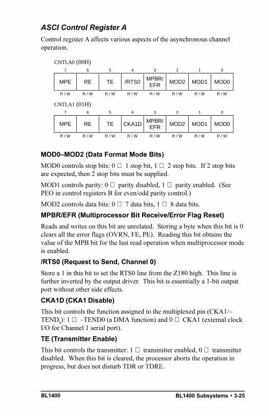
ASCI Control Register A
Control register A affects various aspects of the asynchronous channeloperation.
CNTLA0 (00H)7 6 5 4 3 2 1 0
MPE RE TE /RTS0 MPBR/EFR
MOD2 MOD1 MOD0
R / W R / W R / W R / W R / W R / W R / W R / W
CNTLA1 (01H)7 6 5 4 3 2 1 0
MPE RE TE CKA1D MPBR/EFR
MOD2 MOD1 MOD0
R / W R / W R / W R / W R / W R / W R / W R / W
MOD0MOD2 (Data Format Mode Bits)
MOD0 controls stop bits: 0 ⇒ 1 stop bit, 1 ⇒ 2 stop bits. If 2 stop bitsare expected, then 2 stop bits must be supplied.
MOD1 controls parity: 0 ⇒ parity disabled, 1 ⇒ parity enabled. (SeePEO in control registers B for even/odd parity control.)
MOD2 controls data bits: 0 ⇒ 7 data bits, 1 ⇒ 8 data bits.
MPBR/EFR (Multiprocessor Bit Receive/Error Flag Reset)
Reads and writes on this bit are unrelated. Storing a byte when this bit is 0clears all the error flags (OVRN, FE, PE). Reading this bit obtains thevalue of the MPB bit for the last read operation when multiprocessor modeis enabled.
/RTS0 (Request to Send, Channel 0)
Store a 1 in this bit to set the RTS0 line from the Z180 high. This line isfurther inverted by the output driver. This bit is essentially a 1-bit outputport without other side effects.
CKA1D (CKA1 Disable)
This bit controls the function assigned to the multiplexed pin (CKA1/TEND
0): 1 ⇒ TEND0 (a DMA function) and 0 ⇒ CKA1 (external clock
I/O for Channel 1 serial port).
TE (Transmitter Enable)
This bit controls the transmitter: 1 ⇒ transmitter enabled, 0 ⇒ transmitterdisabled. When this bit is cleared, the processor aborts the operation inprogress, but does not disturb TDR or TDRE.

BL14003-26 s BL1400 Subsystems
RE (Receiver Enable)
This bit controls the receiver: 1 ⇒ enabled, 0 ⇒ disabled. When this bit iscleared, the processor aborts the operation in progress, but does not disturbRDRF or the error flags.
MPE (Multiprocessor Enable)
This bit (1 ⇒ enabled, 0 ⇒ disabled) controls multiprocessor communica-tion mode, which uses an extra bit for selective communication when anumber of processors share a common serial bus. This bit has effect onlywhen MP in Control Register B is set to 1. When this bit is 1, only byteswith the MP bit on will be detected. Others are ignored. If this bit is 0, allbytes received are processed. Ignored bytes do not affect the error flags orRDRF.
ASCI Control Register B
Control Register B for each channel configures multiprocessor mode,parity and baud rate selection.
CNTLB0 (02H) and CNTLB1 (03H)7 6 5 4 3 2 1 0
MPBT MP /CTSPS PEO DR SS2 SS1 SS0
R / W R / W R / W R / W R / W R / W R / W R / W
SS (Source/Speed Select)
Coupled with the prescaler (PS) and the divide ratio (DR), the SS bitsselect the source (internal or external clock) and the baud rate divider, asshown in Table 4-2:
DR (Divide Ratio)
This bit controls one stage of frequency division in the baud-rate generator.If 1, then divide by 64. If 0, then divide by 16. This is the only control bitthat affects the external clock frequency.
PEO (Parity Even/Odd)
This bit affects parity: 0 ⇒ even parity, 1 ⇒ odd parity. It is effective onlyif MOD1 is set in CNTLA (parity enabled).
CTS/PS (Clear to Send/Prescaler)
When read, this bit gives the state of external pin /CTS: 0 ⇒ low,1 ⇒ high. When /CTS pin is high, RDRF is inhibited so that incomingreceive characters are ignored. When written, this bit has an entirelydifferent function. If a 0 is written, the baud rate prescaler is set to divideby 10. If a 1 is written, it is set to divide by 30.

BL1400 BL1400 Subsystems s 3-27
MP (Multiprocessor Mode)
When this bit is set to 1, multiprocessor mode is enabled. The multipro-cessor bit (MPB) is included in transmitted data:
start bit, data bits, MPB, stop bits.
The MPB is 1 when MPBT is 1 and 0 when MPBT is 0.
MPBT (Multiprocessor Bit Transmit)
This bit controls the multiprocessor bit (MPB). When the MPB is 1,transmitted bytes will get the attention of other units listening only forbytes with MPB set.
The prescaler (PS), the divide ratio (DR), and the SS bits form a baud-rategenerator, as shown in Figure 3-14.
Prescaler(PS)×10or×30
ProcessorClock
Divider12...64
DivideRatio(DR)16or64
Ext.Clock
Figure 3-14. Z180 Baud-Rate Generator
Table 3-6 relates ASCI Control Register B to the baud rate. The Z180 inthe BL1400 has a 6.144 MHz clock.
Table 3-6. Baud Rate Dependence onASCI Control Register B
ASCI Control Register BValue
Baud Rate for6.144 MHz Clock
(bps)
00 38,400
01 19,200
02 or 08 9,600
03 or 09 4,800
04 or 0A 2,400
05 or 0B 1,200
06 or 0C 600
0D 300
0E 150

BL14003-28 s BL1400 Subsystems
BL1400 Software Reference s 4-1
SOFTWARE REFERENCE
Chapter 4 describes the software functions available for the BL1400.Most functions are in the BL14_15.LIB; others are found in theDynamic C BIOS in the BL1400s on-board EPROM.
Sections in this chapter include the following topics.
Software Development Options
Programmable Input/Output
Real-Time Clock Integrated Circuit
Serial Communication
Master-Slave Networking
Support Libraries and Sample Programs

BL14004-2 s Software Reference
Software Development Options
Dynamic C Development Software
Two versions of Z-Worlds Dynamic C development software, which runsunder Microsoft Windows, are currently available for the BL1400.
Standard: Maximum 80 Kbytes of code.
This version of Dynamic C is suitable for programs up to 80K withlimited access to extended memory (data items cannot be declared inextended memory).
Deluxe: Maximum 512K of code, 512 Kb of data.
This version supports programs with full access to extended memory.
Dynamic C Manuals
Z-World offers three Dynamic C manuals for programming reference.
Dynamic C Technical Reference
Dynamic C Application Frameworks
Dynamic C Function Reference

BL1400 Software Reference s 4-3
Programmable Input/OutputThe functions described in this section operate the I/O interfaces of theBL1400. Most of these functions are to be found in BL14_15.LIB.Some are in the Dynamic C BIOS (in EPROM).
PIO Ports A and B
PIO Port A is available, all 8 bits, in PIO Modes 0, 1, and 3. PIO Port B isavailable in Mode 3 (bit I/O) only. Bits 47 of port B are always avail-able; bits 3 (RTCCLK) and 2 (RTCDAT) are available if not the real-timeclock is not used. Bits 0 and 1 of port B are dedicated lines, EN485 and/RTCRST respectively.
On power-up, the Dynamic C BIOS configures the PIO Ports A and B toMode 3, with all bits as inputs.. There are four registers for Ports A and B,as shown in Table 4-1.
Table 4-1. PIO Register Names
Register Name Function
PIODA PIO Port A, data
PIOCA PIO Port A, control
PIODB PIO Port B, data
PIOCB PIO Port B, control
Shadow Registers
Dynamic C maintains and uses shadow registers, PIOCAShadow andPIOCBShadow, for both ports. Shadow registers are a standard embedded-systems programming technique. Some of the functions that manipulatethe hardware I/O ports automatically keep a copy of each registers currentconfiguration. If writing routines (especially interrupt-service routines)that temporarily change the configuration of any hardware I/O port, theinterrupt routines first save the appropriate shadow registers beforechanging the ports, and then use the saved shadow-register contents torestore the ports to their original configuration before exiting.
BL14004-4 s Software Reference
Function Prototypes
The following function descriptions follow standard C notation forfunction prototypes. Function prototypes are not examples of how to usea given function. Instead, they modify the names, parameters, and argu-ments of functions with a C-type specifier such as void, byte, and int.In addition, some function prototypes use dummy arguments for param-eters. When using these functions in an application program, do notinclude the type specifiers; instead replace the applicable dummy argu-ments with your own defined arguments.
void setPIOCA( char mask )
Active bits (1s) of mask are set in PIOCAShadow. That result is thensent to PIOCA. Active bits becomes input bits.
PIOCA ← PIOCAShadow ← PIOCAShadow OR mask
void resPIOCA( char mask )
Active bits (1s) of mask are reset in PIOCAShadow. That result is thensent to PIOCA. Active bits becomes output bits.
PIOCA ← PIOCAShadow ← PIOCAShadow AND NOT mask
void setPIODA( char mask )
Active bits (1s) of mask are set in the current output of PIODA.
PIODA ← PIODA OR mask
void resPIODA( char mask )
Active bits (1s) of mask are reset in the current output of PIODA.
PIODA ← PIODA AND NOT mask
void setPIOCB( char mask )
Active bits (1s) of mask are set in PIOCBShadow. That result is thensent to PIOCB. Active bits becomes input bits.
PIOCB ← PIOCBShadow ← PIOCBShadow OR mask
void resPIOCB( char mask )
Active bits (1s) of mask are reset in PIOCBShadow. That result is thensent to PIOCB. Active bits becomes output bits.
PIOCB ← PIOCBShadow ← PIOCBShadow AND NOT mask
void setPIODB( char mask )
Active bits (1s) of mask are set in the current output of PIODB.
PIODB ← PIODB OR mask
BL1400 Software Reference s 4-5
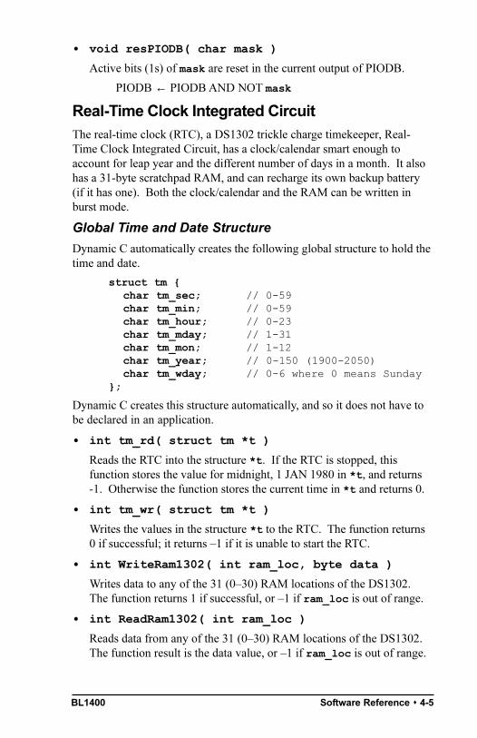
void resPIODB( char mask )
Active bits (1s) of mask are reset in the current output of PIODB.
PIODB ← PIODB AND NOT mask
Real-Time Clock Integrated CircuitThe real-time clock (RTC), a DS1302 trickle charge timekeeper, Real-Time Clock Integrated Circuit, has a clock/calendar smart enough toaccount for leap year and the different number of days in a month. It alsohas a 31-byte scratchpad RAM, and can recharge its own backup battery(if it has one). Both the clock/calendar and the RAM can be written inburst mode.
Global Time and Date Structure
Dynamic C automatically creates the following global structure to hold thetime and date.
struct tm char tm_sec; // 0-59char tm_min; // 0-59char tm_hour; // 0-23char tm_mday; // 1-31char tm_mon; // 1-12char tm_year; // 0-150 (1900-2050)char tm_wday; // 0-6 where 0 means Sunday
;
Dynamic C creates this structure automatically, and so it does not have tobe declared in an application.
int tm_rd( struct tm *t )
Reads the RTC into the structure *t. If the RTC is stopped, thisfunction stores the value for midnight, 1 JAN 1980 in *t, and returns-1. Otherwise the function stores the current time in *t and returns 0.
int tm_wr( struct tm *t )
Writes the values in the structure *t to the RTC. The function returns0 if successful; it returns 1 if it is unable to start the RTC.
int WriteRam1302( int ram_loc, byte data )
Writes data to any of the 31 (030) RAM locations of the DS1302.The function returns 1 if successful, or 1 if ram_loc is out of range.
int ReadRam1302( int ram_loc )
Reads data from any of the 31 (030) RAM locations of the DS1302.The function result is the data value, or 1 if ram_loc is out of range.

BL14004-6 s Software Reference
void WriteBurst1302( void* pdata, int count )
Writes count bytes, in burst mode, to the DS1302, starting at RAMlocation 0. The term pdata points to the data.
void ReadBurst1302( void* pdata, int count )
Reads count bytes, in burst mode, from the DS1302, starting at RAMlocation 0. The term pdata points to a storage area for the data.
void Write1302( int reg, byte data )
Writes data to a specified register of the DS1302.
int Read1302( int reg )
Reads data from a specified register of the DS1302. The functionreturns the data value.
Charger1302( int on_off, int diode, int resistor )
Turns the trickle charger on the DS1302 on (when on_off is non-zero)or off (on_off is 0). The term diode is 1 or 2 for the number ofdiodes on the charging circuit. The term resistor is 2, 4 or 8 for theresistance (in kilohms) of the circuit. If a supercapacitor or a recharge-able battery is connected across VBAT, and GND is charged, then theRTC continues to run and RAM data are not lost when power isremoved from the BL1400.
Do not enable the trickle charge circuit if a nonrecharge-able battery is used to back up the DS1302. The batterycould explode.
555 TimerThe 555 timer, used as an analog input channel to measures resistanceaccording to the formula
∆T = 1.1 RC1 .
Software starts the 555 measurement process, and simultaneously startsone of the Z180 timers. When the 555 finishes its measurement (i.e., after∆T), it trips the timer. The timer value is proportional to R. C
1 is 0.47 µF.
There is a certain amount of overhead in the software, including thesefunctions, which will cause some imprecision in readings. The resistor andcapacitor will vary from their nominal values within a certain tolerance.The finished system may introduce other unpredictable factors. Therefore,Z-World recommends that resistance measurement software be calibrated,on site, if accuracy is important.
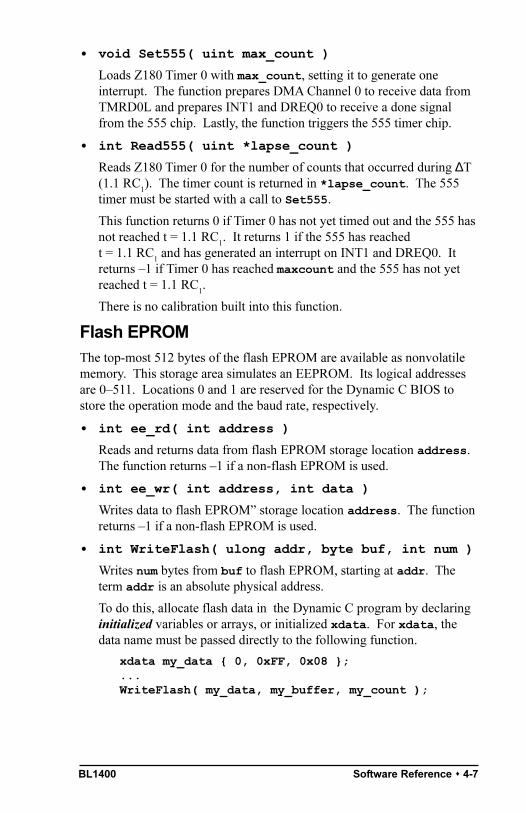
BL1400 Software Reference s 4-7
void Set555( uint max_count )
Loads Z180 Timer 0 with max_count, setting it to generate oneinterrupt. The function prepares DMA Channel 0 to receive data fromTMRD0L and prepares INT1 and DREQ0 to receive a done signalfrom the 555 chip. Lastly, the function triggers the 555 timer chip.
int Read555( uint *lapse_count )
Reads Z180 Timer 0 for the number of counts that occurred during ∆T(1.1 RC
1). The timer count is returned in *lapse_count. The 555
timer must be started with a call to Set555.
This function returns 0 if Timer 0 has not yet timed out and the 555 hasnot reached t = 1.1 RC
1. It returns 1 if the 555 has reached
t = 1.1 RC1 and has generated an interrupt on INT1 and DREQ0. It
returns 1 if Timer 0 has reached maxcount and the 555 has not yetreached t = 1.1 RC
1.
There is no calibration built into this function.
Flash EPROMThe top-most 512 bytes of the flash EPROM are available as nonvolatilememory. This storage area simulates an EEPROM. Its logical addressesare 0511. Locations 0 and 1 are reserved for the Dynamic C BIOS tostore the operation mode and the baud rate, respectively.
int ee_rd( int address )
Reads and returns data from flash EPROM storage location address.The function returns 1 if a non-flash EPROM is used.
int ee_wr( int address, int data )
Writes data to flash EPROM storage location address. The functionreturns 1 if a non-flash EPROM is used.
int WriteFlash( ulong addr, byte buf, int num )
Writes num bytes from buf to flash EPROM, starting at addr. Theterm addr is an absolute physical address.
To do this, allocate flash data in the Dynamic C program by declaringinitialized variables or arrays, or initialized xdata. For xdata, thedata name must be passed directly to the following function.
xdata my_data 0, 0xFF, 0x08 ;...WriteFlash( my_data, my_buffer, my_count );
BL14004-8 s Software Reference
For normal data, the physical address of the data must be passed to thefollowing function.
char xxx[] = 0, 0xFF, 0x08 ;...WriteFlash( phy_adr(xxx), my_buffer, my_count );
RETURN VALUE:
0 if the operation was successful1 if no flash EPROM is present2 if a physical address is within the BIOS area (low 8K)3 if a physical address is within the symbol table4 if the write times out.
If some form of initialization is not included when data are declared,the data will be placed in RAM, not ROM, and this function will notwork.
It may seem contradictory to write to read-only memory. But flashEPROM, despite its name, is not really read-only memory. Writing toflash EPROM, in essence, treats the flash memory as read/write non-volatile memory.
Flash EPROM is rated for 10,000 writes. In practice, flashEPROM has performed for up to 100,000 writes. Z-Worldrecommends that any writes to the flash EPROM be madeby the programmer rather than automatically by thesoftware to maximize the life of the flash EPROM.
!
Serial Communication SoftwareThis section describes functions for Port 0 of the Z180.
Interrupt Handling for Z180 Port 0
Normally, a serial interrupt service routine is declared with the followingcompiler directive.
#INT_VEC SER0_VEC routine
However, if the same serial port is used for Dyamic C programming, theprogram has to be downloaded first with Dynamic C before the address ofthe serial interrupt service routine is loaded into the interrupt vector table.That is, the service routine must be loaded at run-time. The function
reload_vec( int vector, int(*serv_function)() )
will load the address of the service function into the specified location inthe interrupt vector table. In this case, do not the #INT_VEC directive.Once the service routine has taken over, the program cannot be debuged inDynamic C.
BL1400 Software Reference s 4-9
When executable programs are generated for EPROM or for download toRAM, there will be no need for communication with Dynamic C. Thecompile-time directive #INT_VEC can then be used freely.
RS-232 Software Support
int Dinit_z0( void *rbuf, void *tbuf,int rsize, int tsize,byte mode, byte baud,byte modem, byte echo );
Initializes Z180 Port 0 for communication.
PARAMATERS: rbuf is a pointer to the receive buffer.
tbuf is a pointer to the transmit buffer.
rsize is the size of the receive buffer.
tsize is the size of the transmit buffer.
mode selects the operation mode as follows.
bit 0 0 1 stop bit1 2 stop bits
bit 1 0 no parity1 with parity
bit 2 0 7 data bits1 8 data bits
bit 3 0 even parity1 odd parity
bit 4 0 CTS, RTS disabled1 CTS, RTS enabled
baud is the baud rate in multiples of 1200 bps (e.g., specify 8 for9600 bps).
modem If 1, modem is supported. If 0, there is no modem.
echo If 1, every character is echoed. If 0, there is no echoing.
If CTS/RTS handshaking is selected, transmission from the sender isdisabled (by raising RTS) when the receive buffer is 80 % full. Thesoftware lowers RTS (enabling the sender to transmit) when the receivebuffer falls below 20 % of capacity. In a similar manner, a remotesystem can prevent transmission of data by the Z180 Port 0 by assertingits RTS (connected to the Z180 Port 0 CTS).
BL14004-10 s Software Reference
int Dread_z01ch( char* ch )
Reads a character from the circular receive buffer into character ch.
RETURN VALUE:
0 buffer is empty1 byte has been successfully extracted from buffer
int Dwrite_z01ch( char ch )
Places a character in the transmit buffer. If not already transmitting, thefunction initiates transmission.
RETURN VALUE:
0 transmit buffer did not have space for ch1 write was successful
int Dread_z0( char* buffer, char terminate )
Checks the receive buffer for a message terminated with the characterterminate. The message is copied to buffer and terminated with anull character according to the C convention.
RETURN VALUE:
0 no message found with the specified terminating character1 message has been successfully extracted from buffer
int Dwrite_z0( char* buffer, int count )
Copies count bytes from buffer to the transmit buffer. If not alreadytransmitting, the function initiates transmission.
RETURN VALUE:
0 transmit buffer did not have space for count bytes1 write is successful.
void Dz0send_prompt()
Places CR, LF and > in the transmit buffer.
void Dreset_z0rbuf()
Resets the receive buffer.
void Dreset_z0tbuf()
Resets the transmit buffer and stops transmission.
void Dkill_z0()
Turns off Z180 Port 0.
void z0binaryreset()
Sets the serial communication mode to regular ASCII mode. Thismeans that the backspace character is tracked.

BL1400 Software Reference s 4-11
void z0binaryset()
Sets the serial communication mode to binary. This means that all datareceived are placed directly to the receive buffer without preprocessing.
XMODEM Commands
int Dxmodem_z0down( char* buffer, int count )
Sends (downloads) count 128-byte blocks in buffer usingXMODEM protocol.
RETURN VALUE:
0 timed-out (no transfer)1 successful transfer2 canceled transfer (canceled by receiver side)
int Dxmodem_z0up( ulong address, int* pages, int dest, int(*parser)() )
Receives (uploads) a file using XMODEM protocol.
PARAMETERS: address is the physical address in RAM where thereceived data are to be stored. If the receive buffer is allocated byxdata (a Dynamic C keyword to allocate extended memory data), thenthe name of the array may be used for the address argument. If,however, the data area is allocated using normal C, the logicaladdress of the buffer must first be converted to a physical address usingthe library function phy_adr.
pages is the number of 4K blocks of data that have been transferred.
dest If an RS-485 master-slave network is set up, specify dest = 0when the upload is intended for the master. If dest isnon-zero, the upload is intended for the designated slave.
parser is the function that handles parsing of the uploaded data.
RETURN VALUE:
0 timed-out (no transfer)1 successful transfer2 canceled transfer (canceled by sender side)
int z0modemset()
Returns information about modem selection. The function returns 1 ifthe modem option is selected (with Dinit_z0) and 0 if not.
int z0modemstat()
Returns the status of the modem. The function returns 1 if the modemis in command mode and 0 if it is in data mode.
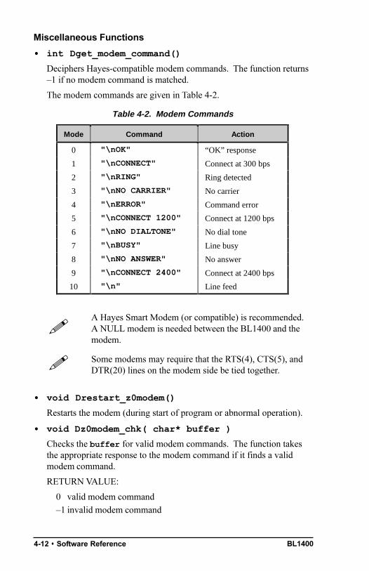
BL14004-12 s Software Reference
Miscellaneous Functions
int Dget_modem_command()
Deciphers Hayes-compatible modem commands. The function returns1 if no modem command is matched.
The modem commands are given in Table 4-2.
Table 4-2. Modem Commands
Mode Command Action
0 "\nOK" “OK” response
1 "\nCONNECT" Connect at 300 bps
2 "\nRING" Ring detected
3 "\nNO CARRIER" No carrier
4 "\nERROR" Command error
5 "\nCONNECT 1200" Connect at 1200 bps
6 "\nNO DIALTONE" No dial tone
7 "\nBUSY" Line busy
8 "\nNO ANSWER" No answer
9 "\nCONNECT 2400" Connect at 2400 bps
10 "\n" Line feed
A Hayes Smart Modem (or compatible) is recommended.A NULL modem is needed between the BL1400 and themodem.
!
Some modems may require that the RTS(4), CTS(5), andDTR(20) lines on the modem side be tied together.!
void Drestart_z0modem()
Restarts the modem (during start of program or abnormal operation).
void Dz0modem_chk( char* buffer )
Checks the buffer for valid modem commands. The function takesthe appropriate response to the modem command if it finds a validmodem command.
RETURN VALUE:
0 valid modem command1 invalid modem command
BL1400 Software Reference s 4-13
void Dz0_circ_int()
This is an interrupt service routine for Z180 Port 0.
void Ddelay_1sec()
Creates adelay of approximately 1 second. suspend(40) is used ifRUNKERNEL is defined.
void Ddelay_100ms()
Creates a delay of approximately 100 ms.
void reload_vec( int vector, int(*function)() )
Loads the address of a function into the interrupt vector table.
This function is only useful during program development, when Z180Port 0 is also used as the Dynamic C programming port. The compile-time interrupt directive can load the serial service functions address inthe interrupt vector table to generate the executable code for EPROMor for download to RAM.
PARAMETERS: vector is the offset for the specific interrupt.
function is a pointer to the interrupt service function.
int getcrc( char* buffer, byte count,int accum )
Computes the CRC (cyclic redundancy check, or check sum) for data inbuffer. Calls to getcrc can be concatenated to compute the CRCfor a large buffer.
PARAMETERS: buffer represents the characters for which tocompute the CRC.
count is the number of characters in buffer, limited to 255, for thisfunction.
accum is the accumulated CRC value from previous computation.
RETURN VALUE: The function returns the integer CRC value.
void resetZ180int()
This is a general reset function that resets, or disables, interrupts for theDMA channels, Z180 serial channels 0 and 1, the PRT timers, theCSIO, INT1, and INT2.
BL14004-14 s Software Reference
Master-Slave Networking
void op_init_z1( char baud, char* rbuf,byte address )
Initializes Z180 Port 1 for RS-485 9th-bit binary communication. Thedata format defaults to 8 bits, no parity, 1 stop bit.
PARAMETERS: baud selects the baud rate in multiples of 1200 bps(specify 16 for 19,200 bps).
rbuf is the receive buffer.
address is the network address of the board: 0 for the master board,1255 for slaves.
int check_opto_command()
Checks for a valid and completed command or reply in the receivebuffer.
RETURN VALUE:
0 if there is no completed command or message available1 if there is a completed command or reply available2 if the completed command or reply has a bad CRC check
int sendOp22( byte dest, char* message,byte len, int delays )
The master sends a message to the slave and waits for a reply. Thefunction puts the message in the following format.
[slave id] [len+2] [ ] [ ]...[ ] [CRC hi][CRC lo]
PARAMETERS: dest is the slave destination (1255).
message is the message.
len is the length of the message. The maximum message length is 251bytes.
delays is the number of delays to wait for the slave reply. Each delayis ~50 ms if the RTK is used. If the RTK is not used, the software-generated delay is approximately 50 ms.
RETURN VALUE:
1 if there is no reply from the slave2 if a completed reply has a bad CRC1 if there is a completed reply with a proper CRC
The slaves reply is stored in the receive buffer initialized withop_init_z1().
BL1400 Software Reference s 4-15
void replyOpto22( char* reply, byte count, int delays )
The slave replies to the masters inquiry. The function puts the reply inthe following format.
[count+2] [ ] [ ]...[ ] [CRC hi] [CRC lo]
PARAMETERS: reply is the slaves reply string.
count is the length of the reply. Because two CRC bytes are appendedat the end, the longest reply is 252 bytes.
delays is the number of delays before the message is transmittedback. Each delay is ~50 ms when the RTK is used. If the RTK is notin use, the software-generated delay is approximately 50 ms.
The delay is implemented with suspend() if the real-time kernel isbeing used. Otherwise, the delay is a software countdown delay.
Miscellaneous Functions
void misticware( char* tbuf, char count )
This is the gateway for RS-485 9th-bit binary communication. Thereceive buffer and the transmit buffer must have been previously set up.Interrupt-driven transmission must be enabled.
PARAMETERS: tbuf is the transmit buffer. Data in the buffer shouldalready be in the correct format
count is the number of bytes to be transmitted
void optodelay()
Produces a delay of ~50 ms. The delay is implemented with suspend()if the real-time kernel is being used. Otherwise, it is a softwarecountdown delay.
int rbuf_there()
Monitors the receive buffer for a completed command or reply.
RETURN VALUE:
1 if a completed command or reply is available0 if a completed command or reply is not available
void op_send_z1( char* tbuf, byte count )
This function is called by misticware() to initiate transmission ofdata.
void op_rec_z1()
This function is called by misticware() to reset and to ready thereceiver to receive data.
BL14004-16 s Software Reference
void op_kill_z1()
Turns off Z180 Port 1. The RS-485 driver is also disabled.
void z1_op_int()
This is an interrupt service routine for the Z180 Port 1 used in master-slave networking.
Support Libraries and Sample ProgramsDynamic C provides libraries and software samples. These softwarelibraries and sample programs are included on the Dynamic C distributiondisk.
DRIVERS.LIB and PLC_EXP.LIB apply to most Z-World controllers. Thelibraries listed in Table 4-3 apply speciifically to the BL1400.
Table 4-3. Dynamic C Libraries
Library Description
Z0232.LIB RS-232 library for Z180 Port 0
BL14_15.LIB Low-level drivers for the BL1400
MODEM232.LIB Miscellaneous functions common to the other communication libraries
NETWORK.LIB RS-485 9-bit binary half-duplex support for Z180 Port 1
Sample Programs
The sample programs listed in Table 4-4 can be found in theSAMPLES\BL14_15 subdirectory in the Dynamic C directory.

BL1400 Software Reference s 4-17
Table 4-4. BL1400 Sample Programs
Program Description
MG485MST.C RS-485 master program that communicates to anotherBL1400 running MG485SLV.C
MG485SLV.C RS-485 slave program that communicates to anotherBL1400 running MG485MST.C
MG555.C Uses Timer0, INT1 and DMA0 to read back theelapsed time when the 555 times out
MG555PIO.C Uses the 555 to time square waves generated out ofthe PIODA bits
MGCHRGER.C Charges a supercapacitor or rechargeable battery withthe DS1302
MGDEMO_RT.C Shows the real-time kernel (RTK) for the BL1400
MGDSRAM.C Writes and reads data from the RAM space of theDS1302
MGFLASH.C Stores data to flash EPROM “initialized data space”
MGFLSHEE.C Writes and reads data from simulated EEPROM ofthe flash EPROM
MGLCD.C Uses PIOA to drive an LCD
MGLCDCG.C Loads and uses special LCD characters
MGLCDKEY.C Uses PIOA and PIOB to drive keypad and print toLCD
MGPIODAC.C Uses bit 2 of PIOA as a simple 10-bit DAC.
MGPIOM0.C Uses PIOA in Mode 0
MGPIOM1.C Uses PIOA in Mode 1
MGPIOM3A.C Uses PIOA in Mode 3
MGPIOM3B.C Uses PIOB in Mode 3
MGPLCDAC.C Uses PIOA to drive an XP8600
MGPLCRLY.C Uses PIOA to drive an XP8300 or an XP8400
MGPLCUIO.C Uses PIOA to drive an XP8200
MGPRTPIO.C Uses PRT0 to time square waves generated out of thePIODA
MGRS-232.C Uses RS-232 port on Z180 Port 0
MGRTC.C Reads and displays time from the real-time clock

BL14004-18 s Software Reference

BL1400 Appendix A: Troubleshooting s A-1
APPENDIX A: TROUBLESHOOTING
Appendix A provides procedures for troubleshooting system hardware andsoftware.
BL1400A-2 s Appendix A: Troubleshooting
Out of the BoxCheck the items listed below before starting development. Recheckingmay help to solve problems found during development.
Verify that the BL1400 runs in standalone mode before connecting anyexpansion boards or I/O devices.
Verify that the entire system has good, low-impedance, separategrounds for analog and digital signals. The BL1400 is often connectedbetween the host PC and another device. Any differences in groundpotential can cause serious problems that are hard to diagnose.
Do not connect analog ground to digital ground anywhere.
Verify that the host PCs COM port works by connecting a known-goodserial device to the COM port. Remember that a PCs COM1/COM3and COM2/COM4 share interrupts. User shells and mouse software, inparticular, often interfere with proper COM-port operation. Forexample, a mouse running on COM1 can preclude running Dynamic Con COM3.
Use the Z-World power supply supplied with the developers kit. Ifanother power supply must be used, verify that it has enough capacityand filtering to support the BL1400.
Use the Z-World cables supplied.
Experiment with each peripheral device connected to the BL1400 inorder to determine how it appears to the BL1400 when powered up,powered down, and/or when its connecting wiring is open or shorted.
Dynamic C Will Not StartIf Dynamic C will not start, an error message on the Dynamic C screen (forexample, Target Not Responding or Communication Error), announcesa communication failure:
Wrong Baud Rate Either Dynamic Cs baud rate is not set correctlyor the BL1400s baud rate is not set correctly. Both baud rates must beidentical. The baud rate is stored in the flash EPROM. Chapter 2described how to change this rate. Dynamic Cs baud rate is set by theSerial Options command in the OPTIONS menu.
Wrong Communication Mode Both the PC and the BL1400 must beusing the same protocol: RS-232. Use Dynamic Cs Serial Optionscommand in the OPTIONS menu to check and alter the protocol for thePC.
BL1400 Appendix A: Troubleshooting s A-3
Wrong COM Port A PC generally has two serial ports, COM1 andCOM2. Specify the one used in the Dynamic C Serial Optionscommand in the OPTIONS menu. Use trial and error, if necessary.
Wrong Operating Mode Communication with Dynamic C is lost ifthe jumpers are set for standalone operation. Reconfigure the board forprogramming as explained in Chapter 2.
Wrong Memory Size Jumpers JP1 and JP2 of the BL1400 specifythe EPROM size. The size of the development board RAM is specifiedwith jumper JP1 on the development board.
If all else fails, connect the serial cable to the BL1400 after power up.If the PCs RS-232 port supplies a large current (most commonly onportable and industrial PCs), some RS-232 level converter ICs go intoa nondestructive latch-up. Connecting the RS-232 cable after power upalleviates this problem.
Dynamic C Loses Serial LinkDynamic C will lose its link if the program disables interrupts for morethan 50 ms. If a communication method is used that is not driven by thenonmaskable interrupt (NMI), make sure that interrupts are not disabledfor more than 50 ms. This is not a concern if a communication methoddriven by NMI is used.
BL1400 Resets RepeatedlyA system reset will occur every 1.2 s if the watchdog timer is not hit.Dynamic C hits the timer, but a user program must include a call tohitwd to make sure the watchdog timer is hit periodically.
Input/Output ProblemsA strobe is needed to move data in PIO modes 0 and 1. The strobe linesare connected to H5 and H6. Use Mode 3 for static input. Mode 1 mayappear to work, but will be erratic because the strobe line floats.
Power-Supply ProblemsIf the external power supply does not have sufficient capacity, an addi-tional load such as an LED can trigger a power-fail interrupt, initiating ahardware reset. The reset triggers the load to be turned off, but then thecomputer restarts and turns the load back on. The oscillation can becorrected by increasing the size of the power supply.

BL1400A-4 s Appendix A: Troubleshooting
Common Programming Errors Values for constants or variables out of range.
Type Range
int –32,768 (–215) to+32,767 (215–1)
long int −2,147,483,648 (−231) to+2147483647 (231−1)
float –6.805646 × 1038 to+6.805646 × 1038
Counting up from, or down to, one instead of zero. In thesoftware world, ordinal series often begin or terminate with zero,not one.
Confusing a functions definition with an instance of its use in alisting.
Not ending statements with semicolons.
Not inserting commas as required in functions parameter lists.
Leaving out an ASCII space character between characters forminga different legalbut unwantedoperator.
Confusing similar-looking operators such as && with &, == with=, // with /, etc.
Inadvertently inserting ASCII nonprinting characters into asource-code file.

BL1400 Appendix B: Specifications s B-1
APPENDIX B: SPECIFICATIONS
Appendix B provides the dimensions and specifications for the BL1400controller.

BL1400B-2 s Appendix B: Specifications
Electrical and Mechanical Specifications
BL1400
Figure B-1 shows the dimensions and the locations of the mounting holesfor the BL1400.
Figure B-1. BL1400 Dimensions
3.2(81)
1.77
5(4
5)
0.125 typ(3.2)
~0.
4(1
0)
~0.
56(1
4)
0.12
5 ty
p(3
.2)
2.0
(51)
0.125 dia, 3x(3.2)
0.15 dia(3.8)
0.15(3.8)
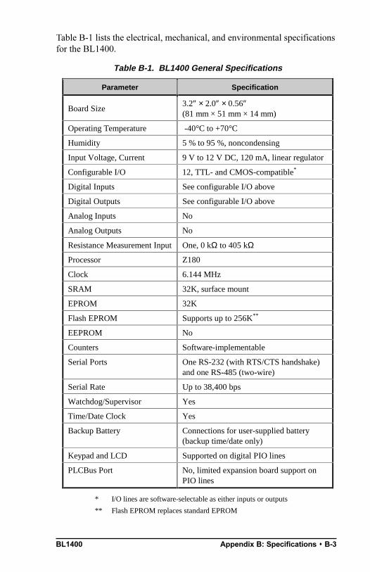
BL1400 Appendix B: Specifications s B-3
Table B-1 lists the electrical, mechanical, and environmental specificationsfor the BL1400.
Table B-1. BL1400 General Specifications
Parameter Specification
Board Size3.2″ × 2.0″ × 0.56″(81 mm × 51 mm × 14 mm)
Operating Temperature -40°C to +70°C
Humidity 5 % to 95 %, noncondensing
Input Voltage, Current 9 V to 12 V DC, 120 mA, linear regulator
Configurable I/O 12, TTL- and CMOS-compatible*
Digital Inputs See configurable I/O above
Digital Outputs See configurable I/O above
Analog Inputs No
Analog Outputs No
Resistance Measurement Input One, 0 kΩ to 405 kΩ
Processor Z180
Clock 6.144 MHz
SRAM 32K, surface mount
EPROM 32K
Flash EPROM Supports up to 256K**
EEPROM No
Counters Software-implementable
Serial Ports One RS-232 (with RTS/CTS handshake)and one RS-485 (two-wire)
Serial Rate Up to 38,400 bps
Watchdog/Supervisor Yes
Time/Date Clock Yes
Backup Battery Connections for user-supplied battery(backup time/date only)
Keypad and LCD Supported on digital PIO lines
PLCBus Port No, limited expansion board support onPIO lines
* I/O lines are software-selectable as either inputs or outputs
** Flash EPROM replaces standard EPROM
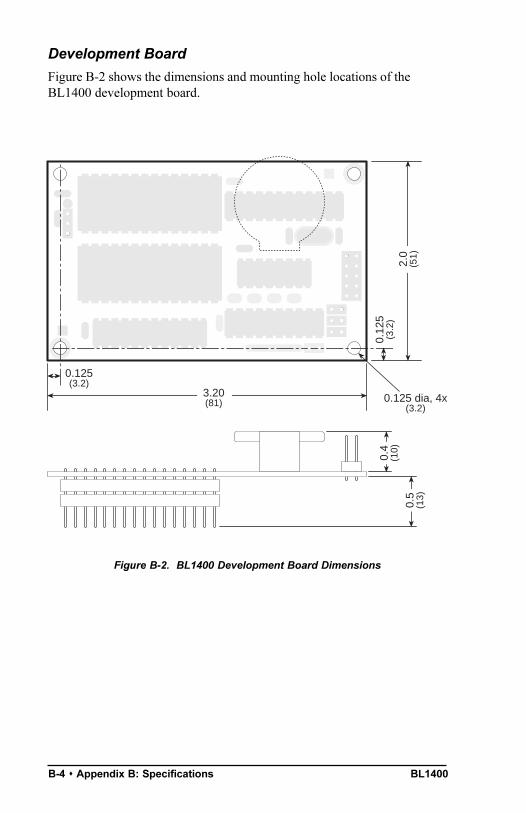
BL1400B-4 s Appendix B: Specifications
Development Board
Figure B-2 shows the dimensions and mounting hole locations of theBL1400 development board.
Figure B-2. BL1400 Development Board Dimensions
0.125(3.2)
3.20(81) 0.125 dia, 4x
(3.2)2.
0(5
1)
0.12
5(3
.2)
0.5
(13)
0.4
(10)
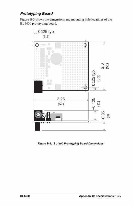
BL1400 Appendix B: Specifications s B-5
Prototyping Board
Figure B-3 shows the dimensions and mounting hole locations of theBL1400 prototyping board.
Figure B-3. BL1400 Prototyping Board Dimensions
2.25(57)
~0.
425
(11)
~0.
35(9
)
0.12
5 ty
p(3
.2)
2.0
(51)
0.125 typ(3.2)

BL1400B-6 s Appendix B: Specifications
Base Plate
Figure B-4 shows the dimensions and mounting hole locations of theBL1400 base plate. The base plate is made from 0.060" aluminum.
6-32 clear, 4x
soa-6-32-6
soa-4-40-6, 3x
0.25 typ(6.4)
3.45(87.6)
0.125 R, typ(3.2)
0.18
5(4
.7)
0.50
(12.
7)
2.75
(70)
2.15
(54.
6)
0.275 typ(7.0)
Figure B-4. BL1400 Base Plate Dimensions

BL1400 Appendix B: Specifications s B-7
ConnectorsBL1400 connectors are not polarized or keyed. Carefully observe connec-tor orientation and pin alignment before making a connection and beforeapplying power.
TemperatureThe BL1400 operates at ambient temperatures from 40°C to +70°C. TheBL1400 may be stored at temperatures from 55°C to +85°C.
PowerThe unregulated input is 9 V to 12 V DC. The maximum power dissipa-tion without additional heat sinking is 1.0 W at 70°C. The BL1400 itselfdraws 120 mA, dissipating about 0.85 W for a 12 V input. Additional heatsinking can be obtained by mounting the BL1400 on the optional alumi-num base plate, or by using aluminum standoffs.
See Appendix C, Power Management, for more informa-tion.$
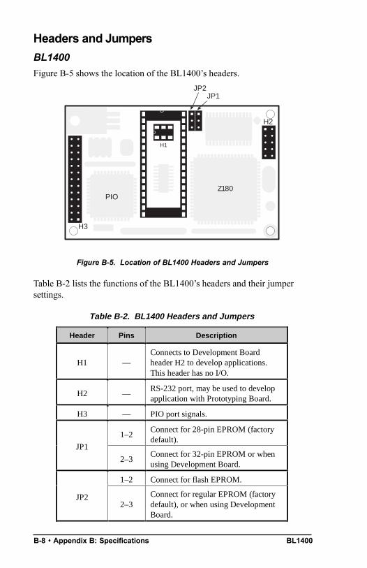
BL1400B-8 s Appendix B: Specifications
Headers and Jumpers
BL1400
Figure B-5 shows the location of the BL1400s headers.
Figure B-5. Location of BL1400 Headers and Jumpers
Z180
U1
PIO
H3
H2
JP1
H1
JP2
Table B-2 lists the functions of the BL1400s headers and their jumpersettings.
Table B-2. BL1400 Headers and Jumpers
Header Pins Description
H1 —Connects to Development Boardheader H2 to develop applications.This header has no I/O.
H2 —RS-232 port, may be used to developapplication with Prototyping Board.
H3 — PIO port signals.
1–2Connect for 28-pin EPROM (factorydefault).
JP1
2–3Connect for 32-pin EPROM or whenusing Development Board.
1–2 Connect for flash EPROM.
JP22–3
Connect for regular EPROM (factorydefault), or when using DevelopmentBoard.
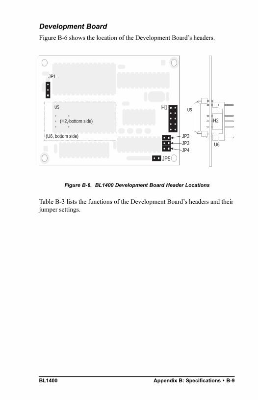
BL1400 Appendix B: Specifications s B-9
Development Board
Figure B-6 shows the location of the Development Boards headers.
Figure B-6. BL1400 Development Board Header Locations
U5
JP4JP3JP2
JP5
JP1
H1
U6
U5
H2(H2, bottom side)
(U6, bottom side)
Table B-3 lists the functions of the Development Boards headers and theirjumper settings.
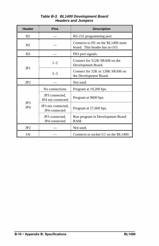
BL1400B-10 s Appendix B: Specifications
Table B-3. BL1400 Development BoardHeaders and Jumpers
Header Pins Description
H1 — RS-232 programming port.
H2 —Connects to H1 on the BL1400 mainboard. This header has no I/O.
H3 — PIO port signals.
1–2Connect for 512K SRAM on theDevelopment Board.
JP1
2–3Connect for 32K or 128K SRAM onthe Development Board.
JP2 — Not used.
No connections Program at 19,200 bps.
JP3 connected,JP4 not connected
Program at 9600 bps.
JP3 not connected,JP4 connected
Program at 57,600 bps.
JP3JP4
JP3 connected,JP4 connected
Run program in Development BoardRAM.
JP2 — Not used.
U6 — Connects to socket U1 on the BL1400.

BL1400 Appendix C: Power Management s C-1
APPENDIX C: POWER MANAGEMENT
Appendix C provides detailed information on power systems and sources.Sections include the following topics.
Direct Current Input
Power Regulator
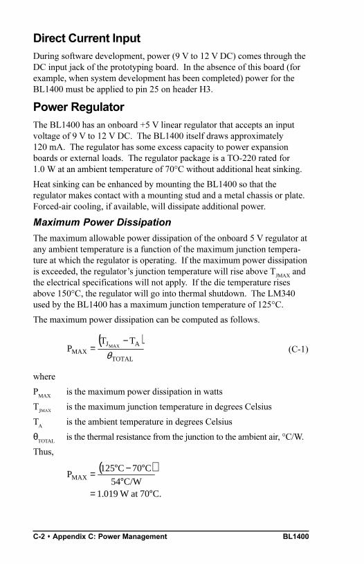
BL1400C-2 s Appendix C: Power Management
Direct Current InputDuring software development, power (9 V to 12 V DC) comes through theDC input jack of the prototyping board. In the absence of this board (forexample, when system development has been completed) power for theBL1400 must be applied to pin 25 on header H3.
Power RegulatorThe BL1400 has an onboard +5 V linear regulator that accepts an inputvoltage of 9 V to 12 V DC. The BL1400 itself draws approximately120 mA. The regulator has some excess capacity to power expansionboards or external loads. The regulator package is a TO-220 rated for1.0 W at an ambient temperature of 70°C without additional heat sinking.
Heat sinking can be enhanced by mounting the BL1400 so that theregulator makes contact with a mounting stud and a metal chassis or plate.Forced-air cooling, if available, will dissipate additional power.
Maximum Power Dissipation
The maximum allowable power dissipation of the onboard 5 V regulator atany ambient temperature is a function of the maximum junction tempera-ture at which the regulator is operating. If the maximum power dissipationis exceeded, the regulators junction temperature will rise above T
JMAX and
the electrical specifications will not apply. If the die temperature risesabove 150°C, the regulator will go into thermal shutdown. The LM340used by the BL1400 has a maximum junction temperature of 125°C.
The maximum power dissipation can be computed as follows.
where
PMAX
is the maximum power dissipation in watts
TJMAX is the maximum junction temperature in degrees Celsius
TA
is the ambient temperature in degrees Celsius
θTOTAL
is the thermal resistance from the junction to the ambient air, °C/W.
Thus,
( )TOTAL
AJMAX
TTP MAX
θ−
= (C-1)
( )
C.70atW019.1C/W54
C70C125PMAX
°=°
°−°=
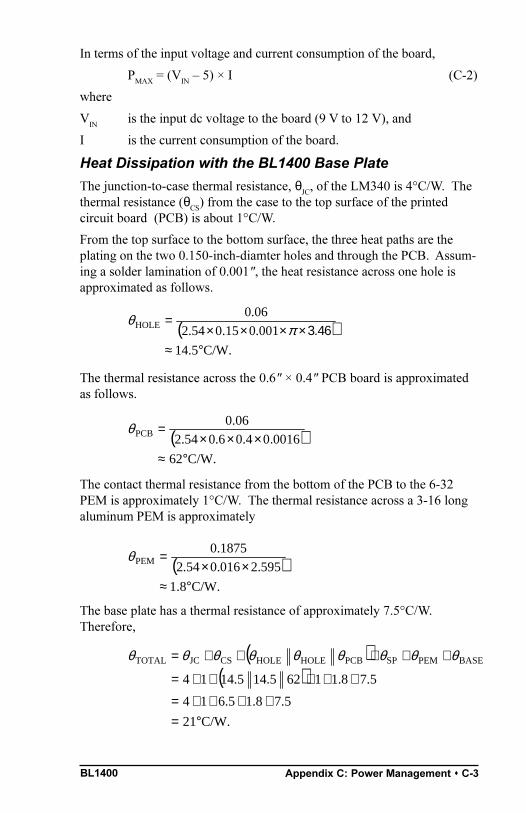
BL1400 Appendix C: Power Management s C-3
In terms of the input voltage and current consumption of the board,
PMAX = (VIN 5) × I (C-2)
where
VIN
is the input dc voltage to the board (9 V to 12 V), and
I is the current consumption of the board.
Heat Dissipation with the BL1400 Base Plate
The junction-to-case thermal resistance, θJC, of the LM340 is 4°C/W. Thethermal resistance (θCS) from the case to the top surface of the printedcircuit board (PCB) is about 1°C/W.
From the top surface to the bottom surface, the three heat paths are theplating on the two 0.150-inch-diamter holes and through the PCB. Assum-ing a solder lamination of 0.001", the heat resistance across one hole isapproximated as follows.
( )C/W.5.14
001.015.054.2
06.0HOLE
°≈3.46××××
=π
θ
The thermal resistance across the 0.6" × 0.4" PCB board is approximatedas follows.
( )C/W.62
001604.06.054.2
06.0PCB
°≈.×××
=θ
The contact thermal resistance from the bottom of the PCB to the 6-32PEM is approximately 1°C/W. The thermal resistance across a 3-16 longaluminum PEM is approximately
( )C/W.8.1
595.2016.054.2
1875.0PEM
°≈××
=θ
The base plate has a thermal resistance of approximately 7.5°C/W.Therefore,
( )( )
C/W.21
5.78.15.614
5.78.11625.145.1414
BASEPEMSPPCBHOLEHOLECSJCTOTAL
°=++++=
+++++=
+++++= θθθθθθθθθ

BL1400C-4 s Appendix C: Power Management
At an ambient temperature of 50°C, the maximum power dissipation is
PMAX
= (125 50) / 21 ≅ 3.57 W.
With VIN
equal to 13 V, the maximum current draw is
I = 3.57 / (13 5) ≅ 446 mA.
Heat Dissipation without the Base Plate
If the BL1400 is to be mounted on a heat-conducting surface, Z-Worldrecommends the following mounting scheme. Use a 6-32 steel screw tohold the regulator to a ¼ 6-32 aluminum standoff mounted on a large heatsink. A conservative estimate of the thermal resistance is as follows.
The thermal resistance across a ¼-6-32 aluminum standoff of ¼ height is
( )( )
C/W.5.17
515.614
511625.145.1414
BASEPEMSPPCBHOLEHOLECSJCTOTAL2
°=++++=
+++++=
+++++= θθθθθθθθθ
C/W.1595.2035.054.2
25.0AL
°=××
=θ
Assuming a basis of 5 °C/W, the total thermal resistance becomes
At an ambient temperature of 50°C, the maximum power dissipation is
PMAX
= (125 50) / 17.5 = 4.28 W.
With VIN
equal to 13 V, the maximum current draw is
I = 4.28 / (13 5) = 535 mA.

BL1400 Appendix D: Prototyping Board s D-1
APPENDIX D: PROTOTYPING BOARD
Appendix D describes the BL1400 Prototyping Board.

BL1400D-2 s Appendix D: Prototyping Board
Prototyping BoardThe BL1400 Prototyping Board was designed to allow the user to experi-ment with the BL1400 and to prototype small circuits that can piggybackon the BL1400. The Prototyping Board has several pre-built subcircuitsthat can be tested or used as part of a custom design. An array of uncom-mitted pads facilitates prototyping. Power rails bring +5 V and GND tothese pads.
The prototyping board has the following features:
Direct Header Connections
Header H1 on the bottom side of the Prototyping Board connects directlyto header H3 of the BL1400.
Array of Pads
An array of pads for dual in-line packages (DIPs) and discrete componentsis provided. Pads and power rails are arranged and interconnected so thatit is easy to place and connect 300-mil or 600-mil DIPs.
Extra Pads
Extra pads bring out signals from header H1 oo the Prototyping Board foreasier soldering.
Figure D-1. BL1400 Prototyping Board
H126-pin
Header(underboard)
SuperCap.
Buzzer
Thermistor
DC Jack
JP2
JP1
Pushbutton Switch
Pushbutton SwitchLED
LED
H2

BL1400 Appendix D: Prototyping Board s D-3
The following list notes some important points about the BL1400:
The prototyping board measures 2.0" × 2.25" (51 mm × 57 mm).
The mounting holes are 0.125" in diameter. Their centers are inset0.125" from the edges of the board.
Signals on header H1 are identical to those on header H3 of BL1400.
Power (9 V to 12 V DC) comes in the jack, through pin 25 of H1, thento the 5 V regulator on the BL1400, and back to the Prototyping Boardon pin 1 (+5 V) of H1.
H2 on the Prototyping Board is nearly identical to H1, but most of thesignal positions on H2 are pads for easy solder connections. Theremaining positions on H2 are jumper pins.
A set of nine test points or pads (shown in Figure D-2) make signalsfrom the demonstration circuits available.
Power rails bring +5 V and GND to the array of pads (see Figure D-3).
Figure D-2. Prototyping Board Signals
Test Points
H2, 26 pins
12345678
9
DCIN
GND, 6 places
H1, 26 pins(bottom side)
+5 V
Figure D-3. Prototyping Board+5 V and GND Connections
GND
Dashed tracesare on theunderside ofthe board
GND
GND
GND
+5 V
+5 V
+5 V
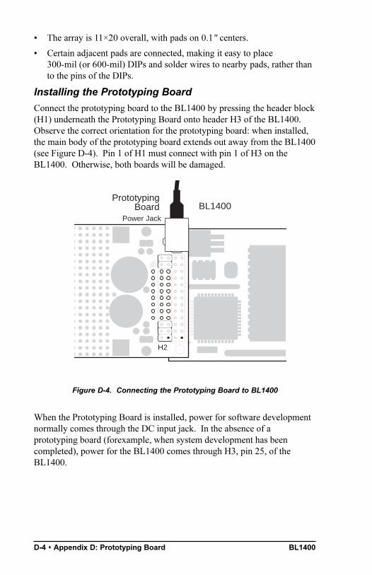
BL1400D-4 s Appendix D: Prototyping Board
The array is 11×20 overall, with pads on 0.1" centers.
Certain adjacent pads are connected, making it easy to place300-mil (or 600-mil) DIPs and solder wires to nearby pads, rather thanto the pins of the DIPs.
Installing the Prototyping Board
Connect the prototyping board to the BL1400 by pressing the header block(H1) underneath the Prototyping Board onto header H3 of the BL1400.Observe the correct orientation for the prototyping board: when installed,the main body of the prototyping board extends out away from the BL1400(see Figure D-4). Pin 1 of H1 must connect with pin 1 of H3 on theBL1400. Otherwise, both boards will be damaged.
Figure D-4. Connecting the Prototyping Board to BL1400
EPROM
PIO
H3 1
BL1400
H2
PrototypingBoard
Power Jack
When the Prototyping Board is installed, power for software developmentnormally comes through the DC input jack. In the absence of aprototyping board (forexample, when system development has beencompleted), power for the BL1400 comes through H3, pin 25, of theBL1400.

BL1400 Appendix D: Prototyping Board s D-5
Sample CircuitsSeveral demonstration circuits are included on the Prototyping Board.
LEDs
LEDs D1 and D2 are turned on when their respective test pads (TP8, TP1)are driven with a low logic level.
Figure D-5. Prototyping Board LEDs
TP8
TP1
D2
D1
470 Ω
470 Ω
Switches
Pushbutton switches SW1 and SW2 are tied to pull-up resistors. Theirrespective test pads (TP3, TP6) are pulled to ground when the switches arepressed.
Figure D-6. Prototyping Board Switches
TP6
SW2
TP3
SW1
10 kΩ 10 kΩ
Jumpers
Jumpers J1 and J2 are tied to pull-up resistors. Their respective test pads(TP2, TP7) are pulled to ground when connectors are installed.
Figure D-7. Prototyping Board Jumpers
TP2
TP7
JP1 JP2
10 kΩ 10 kΩ
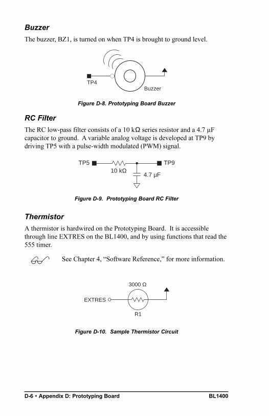
BL1400D-6 s Appendix D: Prototyping Board
Buzzer
The buzzer, BZ1, is turned on when TP4 is brought to ground level.
Figure D-8. Prototyping Board Buzzer
BuzzerTP4
RC Filter
The RC low-pass filter consists of a 10 kΩ series resistor and a 4.7 µFcapacitor to ground. A variable analog voltage is developed at TP9 bydriving TP5 with a pulse-width modulated (PWM) signal.
Figure D-9. Prototyping Board RC Filter
TP9TP5
4.7 µF10 kΩ
Thermistor
A thermistor is hardwired on the Prototyping Board. It is accessiblethrough line EXTRES on the BL1400, and by using functions that read the555 timer.
See Chapter 4, Software Reference, for more information.$
Figure D-10. Sample Thermistor Circuit
EXTRES
R1
3000 Ω

BL1400 Appendix D: Prototyping Board s D-7
The Using Thermistors section in Chapter 3, Interface Overview,discusses the resistance equations and temperature coefficient of a hypo-thetical thermistor. The thermistor used on the Prototyping Board has aresistance of 3000 Ω at 25°C and a temperature coefficient of -4.49% perdegree Celsius. (This is Keystone part RL2007-1723-103-SA, or Digikeypart KC004E-ND.)
For α = 4.49%, ß = (298.15 × 298.15) × 0.0449 = 3991.
The resistance at 25°C is 3000 Ω, and so
650,740A
eA3000 15.298/3991
×==
or
.00461.0650,740
3000A ==
Therefore,
ln A = 5.379
and so
( )
( ) .379.5Rln
3991
AlnRlnT
+=
−= β

BL1400D-8 s Appendix D: Prototyping Board

BL1400 Appendix E: PLCBus s E-1
APPENDIX E: PLCBUS
Appendix E provides the pin assignments for the PLCBus, describes theregisters, and lists the software drivers.
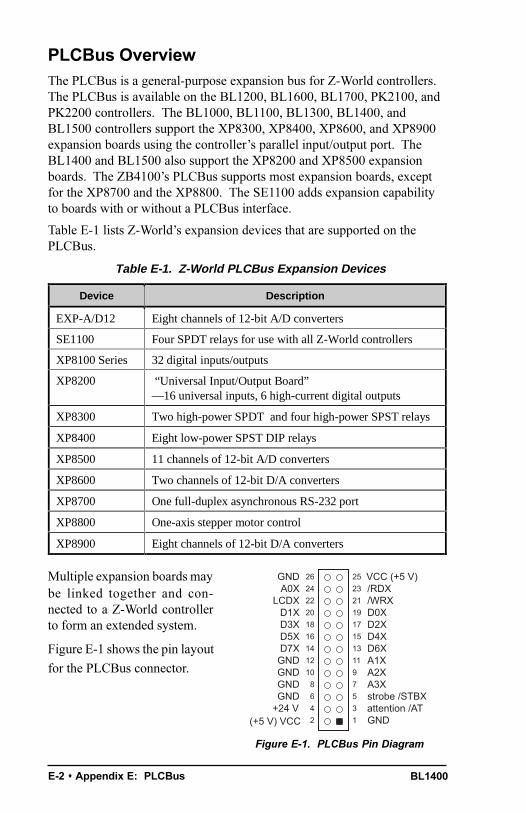
BL1400E-2 s Appendix E: PLCBus
PLCBus OverviewThe PLCBus is a general-purpose expansion bus for Z-World controllers.The PLCBus is available on the BL1200, BL1600, BL1700, PK2100, andPK2200 controllers. The BL1000, BL1100, BL1300, BL1400, andBL1500 controllers support the XP8300, XP8400, XP8600, and XP8900expansion boards using the controllers parallel input/output port. TheBL1400 and BL1500 also support the XP8200 and XP8500 expansionboards. The ZB4100s PLCBus supports most expansion boards, exceptfor the XP8700 and the XP8800. The SE1100 adds expansion capabilityto boards with or without a PLCBus interface.
Table E-1 lists Z-Worlds expansion devices that are supported on thePLCBus.
Multiple expansion boards maybe linked together and con-nected to a Z-World controllerto form an extended system.
Figure E-1 shows the pin layout
for the PLCBus connector.
Table E-1. Z-World PLCBus Expansion Devices
Device Description
EXP-A/D12 Eight channels of 12-bit A/D converters
SE1100 Four SPDT relays for use with all Z-World controllers
XP8100 Series 32 digital inputs/outputs
XP8200 “Universal Input/Output Board”—16 universal inputs, 6 high-current digital outputs
XP8300 Two high-power SPDT and four high-power SPST relays
XP8400 Eight low-power SPST DIP relays
XP8500 11 channels of 12-bit A/D converters
XP8600 Two channels of 12-bit D/A converters
XP8700 One full-duplex asynchronous RS-232 port
XP8800 One-axis stepper motor control
XP8900 Eight channels of 12-bit D/A converters
24
13
6 58 7
10 912 1114 1316 1518 1720 1922 2124 2326 25
GNDD7XD5XD3XD1X
LCDXA0X
GND
GND attention /ATstrobe /STBXGNDA3XGNDA2XGNDA1X
/RDXVCC (+5 V)
D0X/WRX
D4XD2X
D6X
+24 V(+5 V) VCC
Figure E-1. PLCBus Pin Diagram
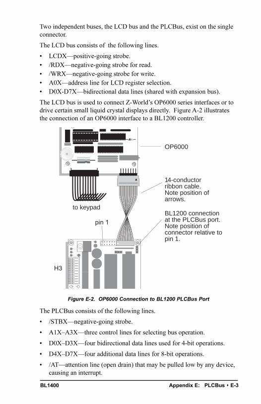
BL1400 Appendix E: PLCBus s E-3
The PLCBus consists of the following lines.
/STBXnegative-going strobe.
A1XA3Xthree control lines for selecting bus operation.
D0XD3Xfour bidirectional data lines used for 4-bit operations.
D4XD7Xfour additional data lines for 8-bit operations.
/ATattention line (open drain) that may be pulled low by any device,causing an interrupt.
pin 1
P1
H3
OP6000
14-conductorribbon cable.Note position ofarrows.
to keypadBL1200 connectionat the PLCBus port.Note position ofconnector relative topin 1.
Figure E-2. OP6000 Connection to BL1200 PLCBus Port
Two independent buses, the LCD bus and the PLCBus, exist on the singleconnector.
The LCD bus consists of the following lines.
LCDXpositive-going strobe. /RDXnegative-going strobe for read. /WRXnegative-going strobe for write. A0Xaddress line for LCD register selection. D0X-D7Xbidirectional data lines (shared with expansion bus).
The LCD bus is used to connect Z-Worlds OP6000 series interfaces or todrive certain small liquid crystal displays directly. Figure A-2 illustratesthe connection of an OP6000 interface to a BL1200 controller.
BL1400E-4 s Appendix E: PLCBus
The PLCBus may be used as a 4-bit bus (D0XD3X) or as an 8-bit bus(D0XD7X). Whether it is used as a 4-bit bus or an 8-bit bus depends onthe encoding of the address placed on the bus. Some PLCBus expansioncards require 4-bit addressing and others (such as the XP8700) require8-bit addressing. These devices may be mixed on a single bus.
There are eight registers corresponding to the modes determined by buslines A1X, A2X, and A3X. The registers are listed in Table E-2.
Table E-2. PLCBus Registers
Register Address A3 A2 A1 Meaning
BUSRD0 C0 0 0 0 Read data, one way
BUSRD1 C2 0 0 1Read data, anotherway
BUSRD2 C4 0 1 0 Spare, or read data
BUSRESET C6 0 1 1Read this register toreset the PLCBus
BUSADR0 C8 1 0 0First address nibbleor byte
BUSADR1 CA 1 0 1Second addressnibble or byte
BUSADR2 CC 1 1 0Third address nibbleor byte
BUSWR CE 1 1 1 Write data
Writing or reading one of these registers takes care of all the bus details.Functions are available in Z-Worlds software libraries to read from orwrite to expansion bus devices.
To communicate with a device on the expansion bus, first select a registerassociated with the device. Then read or write from/to the register. Theregister is selected by placing its address on the bus. Each device recog-nizes its own address and latches itself internally.
A typical device has three internal latches corresponding to the threeaddress bytes. The first is latched when a matching BUSADR0 is de-tected. The second is latched when the first is latched and a matchingBUSADR1 is detected. The third is latched if the first two are latched anda matching BUSADR2 is detected. If 4-bit addressing is used, then thereare three 4-bit address nibbles, giving 12-bit addresses. In addition, aspecial register address is reserved for address expansion. This address, ifever used, would provide an additional four bits of addressing when usingthe 4-bit convention.

BL1400 Appendix E: PLCBus s E-5
If eight data lines are used, then the addressing possibilities of the busbecome much greatermore than 256 million addresses according to theconventions established for the bus.
Place an address on the bus by writing (bytes) to BUSADR0, BUSADR1and BUSADR2 in succession. Since 4-bit and 8-bit addressing modesmust coexist, the lower four bits of the first address byte (written toBUSADR0) identify addressing categories, and distinguish 4-bit and 8-bitmodes from each other.
There are 16 address categories, as listed in Table E-3. An x indicatesthat the address bit may be a 1 or a 0.
Table E-3. First-Level PLCBus Address Coding
First Byte Mode Addresses Full Address Encoding
– – – – 0 0 0 0– – – – 0 0 0 1– – – – 0 0 1 0– – – – 0 0 1 1
4 bits × 3 256256256256
0000 xxxx xxxx0001 xxxx xxxx0010 xxxx xxxx0011 xxxx xxxx
– – – x 0 1 0 0– – – x 0 1 0 1– – – x 0 1 1 0– – – x 0 1 1 1
5 bits × 3 2,0482,0482,0482,048
x0100 xxxxx xxxxxx0101 xxxxx xxxxxx0110 xxxxx xxxxxx0111 xxxxx xxxxx
– – x x 1 0 0 0– – x x 1 0 0 1
6 bits × 3 16,38416,384
xx1000 xxxxxx xxxxxxxx1001 xxxxxx xxxxxx
– – x x 1 0 1 0 6 bits × 1 4 xx1010
– – – – 1 0 1 1 4 bits × 1 1 1011 (expansion register)
x x x x 1 1 0 0 8 bits × 2 4,096 xxxx1100 xxxxxxxx
x x x x 1 1 0 1 8 bits × 3 1M xxxx1101 xxxxxxxx xxxxxxxx
x x x x 1 1 1 0 8 bits × 1 16 xxxx1110
x x x x 1 1 1 1 8 bits × 1 16 xxxx1111
This scheme uses less than the full addressing space. The mode notationindicates how many bus address cycles must take place and how many bitsare placed on the bus during each cycle. For example, the 5 × 3 modemeans three bus cycles with five address bits each time to yield 15-bitaddresses, not 24-bit addresses, since the bus uses only the lower five bitsof the three address bytes.
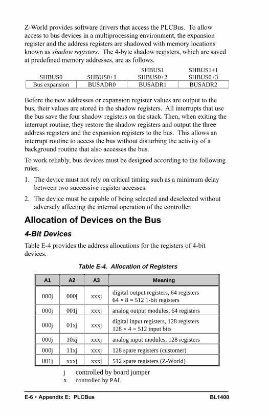
BL1400E-6 s Appendix E: PLCBus
Z-World provides software drivers that access the PLCBus. To allowaccess to bus devices in a multiprocessing environment, the expansionregister and the address registers are shadowed with memory locationsknown as shadow registers. The 4-byte shadow registers, which are savedat predefined memory addresses, are as follows.
SHBUS1 SHBUS1+1SHBUS0 SHBUS0+1 SHBUS0+2 SHBUS0+3
Bus expansion BUSADR0 BUSADR1 BUSADR2
Before the new addresses or expansion register values are output to thebus, their values are stored in the shadow registers. All interrupts that usethe bus save the four shadow registers on the stack. Then, when exiting theinterrupt routine, they restore the shadow registers and output the threeaddress registers and the expansion registers to the bus. This allows aninterrupt routine to access the bus without disturbing the activity of abackground routine that also accesses the bus.
To work reliably, bus devices must be designed according to the followingrules.
1. The device must not rely on critical timing such as a minimum delaybetween two successive register accesses.
2. The device must be capable of being selected and deselected withoutadversely affecting the internal operation of the controller.
Allocation of Devices on the Bus
4-Bit Devices
Table E-4 provides the address allocations for the registers of 4-bitdevices.
Table E-4. Allocation of Registers
A1 A2 A3 Meaning
000j 000j xxxjdigital output registers, 64 registers64 × 8 = 512 1-bit registers
000j 001j xxxj analog output modules, 64 registers
000j 01xj xxxjdigital input registers, 128 registers128 × 4 = 512 input bits
000j 10xj xxxj analog input modules, 128 registers
000j 11xj xxxj 128 spare registers (customer)
001j xxxj xxxj 512 spare registers (Z-World)
j controlled by board jumperx controlled by PAL
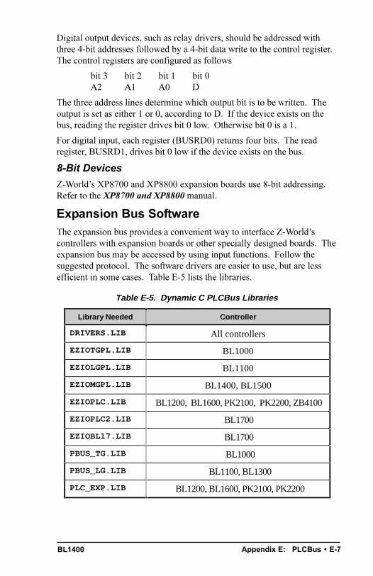
BL1400 Appendix E: PLCBus s E-7
Digital output devices, such as relay drivers, should be addressed withthree 4-bit addresses followed by a 4-bit data write to the control register.The control registers are configured as follows
bit 3 bit 2 bit 1 bit 0A2 A1 A0 D
The three address lines determine which output bit is to be written. Theoutput is set as either 1 or 0, according to D. If the device exists on thebus, reading the register drives bit 0 low. Otherwise bit 0 is a 1.
For digital input, each register (BUSRD0) returns four bits. The readregister, BUSRD1, drives bit 0 low if the device exists on the bus.
8-Bit Devices
Z-Worlds XP8700 and XP8800 expansion boards use 8-bit addressing.Refer to the XP8700 and XP8800 manual.
Expansion Bus SoftwareThe expansion bus provides a convenient way to interface Z-Worldscontrollers with expansion boards or other specially designed boards. Theexpansion bus may be accessed by using input functions. Follow thesuggested protocol. The software drivers are easier to use, but are lessefficient in some cases. Table E-5 lists the libraries.
Table E-5. Dynamic C PLCBus Libraries
Library Needed Controller
DRIVERS.LIB All controllers
EZIOTGPL.LIB BL1000
EZIOLGPL.LIB BL1100
EZIOMGPL.LIB BL1400, BL1500
EZIOPLC.LIB BL1200, BL1600, PK2100, PK2200, ZB4100
EZIOPLC2.LIB BL1700
EZIOBL17.LIB BL1700
PBUS_TG.LIB BL1000
PBUS_LG.LIB BL1100, BL1300
PLC_EXP.LIB BL1200, BL1600, PK2100, PK2200
BL1400E-8 s Appendix E: PLCBus
There are 4-bit and 8-bit drivers. The 4-bit drivers employ the followingcalls.
void eioResetPlcBus()
Resets all expansion boards on the PLCBus. When using this call,make sure there is sufficient delay between this call and the first accessto an expansion board.
LIBRARY: EZIOPLC.LIB, EZIOPLC2.LIB, EZIOMGPL.LIB.
void eioPlcAdr12( unsigned addr )
Specifies the address to be written to the PLCBus using cyclesBUSADR0, BUSADR1, and BUSADR2.
PARAMETER: addr is broken into three nibbles, and one nibble iswritten in each BUSADRx cycle.
LIBRARY: EZIOPLC.LIB, EZIOPLC2.LIB, EZIOMGPL.LIB.
void set16adr( int adr )
Sets the current address for the PLCBus. All read and write operationsaccess this address until a new address is set.
PARAMETER: adr is a 16-bit physical address. The high-ordernibble contains the value for the expansion register, and the remainingthree 4-bit nibbles form a 12-bit address (the first and last nibbles mustbe swapped).
LIBRARY: DRIVERS.LIB.
void set12adr( int adr )
Sets the current address for the PLCBus. All read and write operationsaccess this address until a new address is set.
PARAMETER: adr is a 12-bit physical address (three 4-bit nibbles)with the first and third nibbles swapped.
LIBRARY: DRIVERS.LIB.
void eioPlcAdr4( unsigned addr )
Specifies the address to be written to the PLCBus using only cycleBUSADR2.
PARAMETER: addr is the nibble corresponding to BUSADR2.
LIBRARY: EZIOPLC.LIB, EZIOPLC2.LIB, EZIOMGPL.LIB.

BL1400 Appendix E: PLCBus s E-9
void set4adr( int adr )
Sets the current address for the PLCBus. All read and write operationsaccess this address until a new address is set.
A 12-bit address may be passed to this function, but only the last fourbits will be set. Call this function only if the first eight bits of theaddress are the same as the address in the previous call to set12adr.
PARAMETER: adr contains the last four bits (bits 811) of thephysical address.
LIBRARY: DRIVERS.LIB.
char _eioReadD0( )
Reads the data on the PLCBus in the BUSADR0 cycle.
RETURN VALUE: the byte read on the PLCBus in the BUSADR0cycle.
LIBRARY: EZIOPLC.LIB, EZIOPLC2.LIB, EZIOMGPL.LIB.
char _eioReadD1( )
Reads the data on the PLCBus in the BUSADR1 cycle.
RETURN VALUE: the byte read on the PLCBus in the BUSADR1cycle.
LIBRARY: EZIOPLC.LIB, EZIOPLC2.LIB, EZIOMGPL.LIB.
char _eioReadD2( )
Reads the data on the PLCBus in the BUSADR2 cycle.
RETURN VALUE: the byte read on the PLCBus in the BUSADR2cycle.
LIBRARY: EZIOPLC.LIB, EZIOPLC2.LIB, EZIOMGPL.LIB.
char read12data( int adr )
Sets the current PLCBus address using the 12-bit adr, then reads fourbits of data from the PLCBus with BUSADR0 cycle.
RETURN VALUE: PLCBus data in the lower four bits; the upper bitsare undefined.
LIBRARY: DRIVERS.LIB.

BL1400E-10 s Appendix E: PLCBus
char read4data( int adr )
Sets the last four bits of the current PLCBus address using adr bits 811, then reads four bits of data from the bus with BUSADR0 cycle.
PARAMETER: adr bits 811 specifies the address to read.
RETURN VALUE: PLCBus data in the lower four bits; the upper bitsare undefined.
LIBRARY: DRIVERS.LIB.
void _eioWriteWR( char ch)
Writes information to the PLCBus during the BUSWR cycle.
PARAMETER: ch is the character to be written to the PLCBus.
LIBRARY: EZIOPLC.LIB, EZIOPLC2.LIB, EZIOMGPL.LIB.
void write12data( int adr, char dat )
Sets the current PLCBus address, then writes four bits of data to thePLCBus.
PARAMETER: adr is the 12-bit address to which the PLCBus is set.
dat (bits 03) specifies the data to write to the PLCBus.
LIBRARY: DRIVERS.LIB.
void write4data( int address, char data )
Sets the last four bits of the current PLCBus address, then writes fourbits of data to the PLCBus.
PARAMETER: adr contains the last four bits of the physical address(bits 811).
dat (bits 03) specifies the data to write to the PLCBus.
LIBRARY: DRIVERS.LIB.
The 8-bit drivers employ the following calls.
void set24adr( long address )
Sets a 24-bit address (three 8-bit nibbles) on the PLCBus. All read andwrite operations will access this address until a new address is set.
PARAMETER: address is a 24-bit physical address (for 8-bit bus)with the first and third bytes swapped (low byte most significant).
LIBRARY: DRIVERS.LIB.
BL1400 Appendix E: PLCBus s E-11
void set8adr( long address )
Sets the current address on the PLCBus. All read and write operationswill access this address until a new address is set.
PARAMETER: address contains the last eight bits of the physicaladdress in bits 1623. A 24-bit address may be passed to this function,but only the last eight bits will be set. Call this function only if the first16 bits of the address are the same as the address in the previous call toset24adr.
LIBRARY: DRIVERS.LIB.
int read24data0( long address )
Sets the current PLCBus address using the 24-bit address, then readseight bits of data from the PLCBus with a BUSRD0 cycle.
RETURN VALUE: PLCBus data in lower eight bits (upper bits 0).
LIBRARY: DRIVERS.LIB.
int read8data0( long address )
Sets the last eight bits of the current PLCBus address using address bits1623, then reads eight bits of data from the PLCBus with a BUSRD0cycle.
PARAMETER: address bits 1623 are read.
RETURN VALUE: PLCBus data in lower eight bits (upper bits 0).
LIBRARY: DRIVERS.LIB.
void write24data( long address, char data )
Sets the current PLCBus address using the 24-bit address, then writeseight bits of data to the PLCBus.
PARAMETERS: address is 24-bit address to write to.
data is data to write to the PLCBus.
LIBRARY: DRIVERS.LIB.
void write8data( long address, char data )
Sets the last eight bits of the current PLCBus address using address bits1623, then writes eight bits of data to the PLCBus.
PARAMETERS: address bits 1623 are the address of the PLCBusto write.
data is data to write to the PLCBus.
LIBRARY: DRIVERS.LIB.

BL1400E-12 s Appendix E: PLCBus

Appendix F: Simulated PLCBus Connection s F-1BL1400
APPENDIX F:
SIMULATED PLCBUS CONNECTION
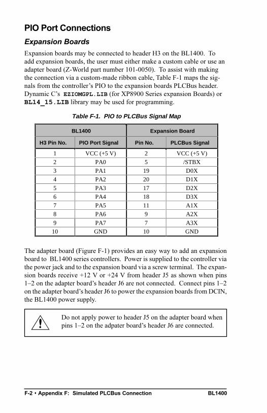
F-2 s Appendix F: Simulated PLCBus Connection BL1400
Table F-1. PIO to PLCBus Signal Map
BL1400 Expansion Board
H3 Pin No. PIO Port Signal Pin No. PLCBus Signal
1 VCC (+5 V) 2 VCC (+5 V)
2 PA0 5 /STBX
3 PA1 19 D0X
4 PA2 20 D1X
5 PA3 17 D2X
6 PA4 18 D3X
7 PA5 11 A1X
8 PA6 9 A2X
9 PA7 7 A3X
10 GND 10 GND
PIO Port Connections
Expansion Boards
Expansion boards may be connected to header H3 on the BL1400. Toadd expansion boards, the user must either make a custom cable or use anadapter board (Z-World part number 101-0050). To assist with makingthe connection via a custom-made ribbon cable, Table F-1 maps the sig-nals from the controllers PIO to the expansion boards PLCBus header.Dynamic Cs EZIOMGPL.LIB (for XP8900 Series expansion Boards) orBL14_15.LIB library may be used for programming.
The adapter board (Figure F-1) provides an easy way to add an expansionboard to BL1400 series controllers. Power is supplied to the controller viathe power jack and to the expansion board via a screw terminal. The expan-sion boards receive +12 V or +24 V from header J5 as shown when pins12 on the adapter boards header J6 are not connected. Connect pins 12on the adapter boards header J6 to power the expansion boards from DCIN,the BL1400 power supply.
Do not apply power to header J5 on the adapter board whenpins 12 on the adpater boards header J6 are connected.

Appendix F: Simulated PLCBus Connection s F-3BL1400
Adapter Board +VGND
J6
J6R2 R1
J2
J1J8
J5J4
J3
BL1400
Exp
ansi
on B
oard
BL1400 PowerSupply
Expansion BoardPower Supply
H3
To LCD
Figure F-1. Adapter Board Connections
If either J2 or J3 on the adapter board is used, some of thesignals on J8 are inaccesible. J8s RS-485 and RMI signalsremain available.
!
Liquid Crystal Displays and Keypads
Liquid crystal displays (LCDs) can also be connected to the BL1400s PIOport on header H3 using the adapter board. The LCD must be hardwiredfor writing only. Table F-2 lists the wiring connections. for LCDs.
Only the LCDs EN line is exclusive to the LCD. RS and the other datalines can be shared with other devices. The LCD busy flag is never checked.Instead, a 40 µs software delay ensures that the LCD is not busy beforewriting to the LCD.
Table F-3 lists the wiring connections for keypads.

F-4 s Appendix F: Simulated PLCBus Connection BL1400
Table F-2. PIO to LCD Signal Map
BL1400 2 × 20 LCD
H3 Pin No. PIO Port Signal Pin No. Signal
1 VCC (+5 V) 2 VDD
4 PA2 4 RS
5 PA3 6 EN
— — 7 DB0
— — 8 DB1
— — 9 DB2
— — 10 DB3
6 PA4 11 DB4
7 PA5 12 DB5
8 PA6 13 DB6
9 PA7 14 DB7
10 GND 3 VO*
5 RD/WR26 GND
1 VSS
* To improve contrast, connect VO to +0.3 V by adding a resistor betweenV0 and GND instead of connecting VO to GND.
Table F-3. PIO to Keypad Signal Map
BL1400
H3 Pin No. PIO Port SignalKeypad Signal
2 PA0 KeyRead 1
3 PA1 KeyRead 2
6 PA4 DriveLine 1
7 PA5 DriveLine 2
8 PA6 DriveLine 3
9 PA7 DriveLine 4
13 PB7 KeyRead 6
14 PB6 KeyRead 5
15 PB5 KeyRead 4
16 PB4 KeyRead 3

Appendix F: Simulated PLCBus Connection s F-5BL1400
Software Drivers
Using Expansion Boards with PIO Port A
A PLCBus driver is implemented using the 8-bit PIO Port A (PIOA).With the BL1400, the developer is limited to 4-bit PLCBus peripherals.An attention line (/AT) is not available. The wiring connections shown inTable F-1 are used.
For multiply threaded programs, be sure to save and to restore the state ofthe PLCBus when entering a thread that can preempt other threads thatalso use the PLCBus. The function mgsave_pbus saves PLCBus stateto the stack and mgrestore_pbus restores it from the stack.
void mgset12adr( int addr )
Sets the current address of the PLCBus. A subsequent read or write ofthe PLCBus will access the expansion board with this address. Theaddress remains in effect until a new address is set. The term addr isthe 12-bit physical address of the PLCBus expansion board. Thelowest 4-bit nibble is transmitted last (as BUSADR2). The thirdnibble is transmitted first (as BUSADR0).
void mgset12data( int addr, int data )
Writes data to the expansion board at addr. Only the lowest four bitsof data are useable (for BUSWR).
int mgread12data0( int addr )
Reads data (with BUSRD0) from the expansion board at addr. Thefunction result holds the data.
int mgread12data1( int addr )
Reads data (with BUSRD1) from the expansion board at addr. Thefunction result holds the data.
int mgread12data2( int addr )
Reads data (with BUSRD2) from the expansion board at addr. Thefunction result holds the data.
void mgwrite4data( int value )
Writes the low 4 bits of value (with BUSWR) to an expansion board.This function assumes that the expansion boards address has beenplaced on the PLCBus (with mgset12adr).
void mgreset_pbus()
Initializes PIO Port A to communicate with expansion boards. Thefunction also resets all expansion boards.

F-6 s Appendix F: Simulated PLCBus Connection BL1400
Refer to the XP8300, XP8400 and SE1100 Users Manualfor details regarding devices and device numbering schemes.$
Refer to the XP8300, XP8400 and SE1100 Users Manualfor details regarding devices and device numbering schemes.$
Refer to the XP8100 and XP8200 Users Manual for detailsregarding devices and device numbering schemes.$
int mgplc_poll_node( int addr )
Polls for the presence of an expansion board with the given boardaddress. The function returns 1 if the board is found and 0 if the boardis not found.
void mgsave_pbus()
Saves the current state of the PLCBus to the stack. This functionshould only be called in tandem with mgrestore_pbus. Otherwise,the stack will become unbalanced.
void mgrestore_pbus()
Restores the current state of the PLCBus from the stack. This functionshould only be called in tandem with mgsave_pbus. Otherwise, thestack will become unbalanced.
void mgplc_set_relay( int number, int relay,int state )
Turns a relay on an expansion board on or off. The relay board mustbe a Z-World XP8300 or XP8400 expansion board and its numbermust be from 0 to 63. The term relay selects the relay on the selectedboard (05 for XP8300 boards and 07 for XP8400 boards. The termstate is 1 to turn on the relay board and 0 to turn it off.
int mgplcrly_board( int number )
Computes the physical address of a relay board from its board number.The number must be from 0 to 63. (Board number 0 corresponds toaddress 0x000; board number 63 corresponds to address 0x11F.) Thereturn value has the third and the first nibbles interchanged.
int mgplcuio_board( int number )
Computes the physical address of an XP8200 expansion board from itsboard number. The number must be from 0 to 15. (Board number 0corresponds to address 0x040. Board number 15 corresponds toaddress 0x04F.) The return value has the third and the first nibblesinterchanged.
Appendix F: Simulated PLCBus Connection s F-7BL1400
Refer to the XP8600 and XP8900 Users Manual for detailsregarding devices and device numbering schemes.$
int mgplc_dac_board( int number )
Computes the physical address of an XP8600 or XP8900 expansionboard from its board number. The number must be from 0 to 63.(Board number 0 corresponds to address 0x020; board number 63corresponds to address 0x13F.) The return value has the third and thefirst nibbles interchanged.
void mginit_dac()
Initializes an XP8600 or XP8900 expansion board on the PLCBus.This function assumes that the boards address has been placed on thebus (with mgset12adr).
void mgwrite_dac1( int value )
Writes the 12-bit integer value to Register A of DAC 1 of an XP8600or XP8900 expansion board on the PLCBus. This function assumesthat the boards address has been placed on the bus (with mgset12adr).The an XP8600 or XP8900 expansion board does not produce a newconversion value until a call to mglatch_dac1 is executed.
void mglatch_dac1()
Moves Register A data to Register B of DAC 1 of an XP8600 orXP8900 expansion board on the PLCBus. The actual DAC 1 output isconverted from Register B. This function assumes that the boardsaddress has been placed on the bus (with mgset12adr). Be sure thatRegister A contains valid data. See mgwrite_dac1 above.
void mgset_dac1( int value )
Writes a 12-bit integer value to Register A, then moves the data fromRegister A to Register B of DAC 1 of a selected XP8600 or XP8900expansion board. This function assumes that the boards address hasbeen placed on the bus (with mgset12adr). It combines the effect ofmgwrite_dac1 and mglatch_dac1.
void mgwrite_dac2( int value )
Writes the 12-bit integer value to Register A of DAC 2 of an XP8600or XP8900 expansion board on the PLCBus. This function assumesthat the boards address has been placed on the bus (withmgset12adr). The XP8600 or XP8900 expansion board does notproduce a new conversion value until a call to mglatch_dac2 isexecuted.

F-8 s Appendix F: Simulated PLCBus Connection BL1400
void mglatch_dac2()
Moves Register A data to Register B of DAC 2 of an XP8600 orXP8900 expansion board on the PLCBus. The actual DAC 2 output isconverted from Register B. This function assumes that the boardsaddress has been placed on the bus (with mgset12adr). Be sure thatRegister A contains valid data. See mgwrite_dac2 above.
void mgset_dac2( int value )
Writes a 12-bit integer value to Register A, then moves the data fromRegister A to Register B of DAC 2 of a selected XP8600 or XP8900expansion board. This function assumes that the boards address hasbeen placed on the bus (with mgset12adr). It combines the effect ofmgwrite_dac2 and mglatch_dac2.
Using an LCD with PIO Port A
A 4-bit LCD (liquid crystal display) driver is implemented through six bitsof PIO Port A.
The LCD drivers are compatible with the keypad drivers in the followingsection. That is, both an LCD and a keypad can be driven with thissoftware and a BL1400.
void lc_char( byte data )
Writes a character to the LCD.
void lc_ctrl( byte cmd )
Writes a control command to the LCD.
void lc_init()
Initialize the LCD and accessory variables. The LCD uses PIO Port A.
void lc_cgram( void* ptr )
Loads up to eight special characters to the character generator of theLCD from the byte array *p. The first byte in the array is the numberof bytes to store (at 8 bytes per character), with a maximum value of 64for 8 characters. The character codes for the special characters are 0,1, 2, 3, 4, 5, 6, and 7.
void lc_printf( char* format, ... )
This function works like printf, but for the LCD. The escape se-quences shown in Table F-4 are also implemented.
The escape character code is 0x1B.
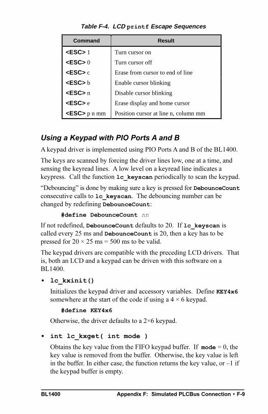
Appendix F: Simulated PLCBus Connection s F-9BL1400
Table F-4. LCD printf Escape Sequences
Command Result
<ESC> 1 Turn cursor on
<ESC> 0 Turn cursor off
<ESC> c Erase from cursor to end of line
<ESC> b Enable cursor blinking
<ESC> n Disable cursor blinking
<ESC> e Erase display and home cursor
<ESC> p n mm Position cursor at line n, column mm
Using a Keypad with PIO Ports A and B
A keypad driver is implemented using PIO Ports A and B of the BL1400.
The keys are scanned by forcing the driver lines low, one at a time, andsensing the keyread lines. A low level on a keyread line indicates akeypress. Call the function lc_keyscan periodically to scan the keypad.
Debouncing is done by making sure a key is pressed for DebounceCountconsecutive calls to lc_keyscan. The debouncing number can bechanged by redefining DebounceCount:
#define DebounceCount nn
If not redefined, DebounceCount defaults to 20. If lc_keyscan iscalled every 25 ms and DebounceCount is 20, then a key has to bepressed for 20 × 25 ms = 500 ms to be valid.
The keypad drivers are compatible with the preceding LCD drivers. Thatis, both an LCD and a keypad can be driven with this software on aBL1400.
lc_kxinit()
Initializes the keypad driver and accessory variables. Define KEY4x6somewhere at the start of the code if using a 4 × 6 keypad.
#define KEY4x6
Otherwise, the driver defaults to a 2×6 keypad.
int lc_kxget( int mode )
Obtains the key value from the FIFO keypad buffer. If mode = 0, thekey value is removed from the buffer. Otherwise, the key value is leftin the buffer. In either case, the function returns the key value, or 1 ifthe keypad buffer is empty.

F-10 s Appendix F: Simulated PLCBus Connection BL1400
For more information or assistance, call a Z-WorldTechnical Support Representative at (530) 757-3737.(
void lc_keyscan()
Scans the 4 × 6 or 2 × 6 keypad. A valid key has to be persistent forDebounceCount calls to lc_keyscan. The function puts validkeypresses into the keypad FIFO buffer. The software will access thesekeypresses using lc_kxget.

BL1400 Appendix G: I/O Maps and Interrupt Vectors s G-1
APPENDIX G: INPUT/OUTPUT MAPS
AND INTERRUPT VECTORS
Appendix G provides information on the BL1400s input/output maps andinterrupt vectors.

BL1400G -2 s Appendix G: I/O Maps and Interrupt Vectors
Memory Map
Internal Input/Output Registers
The internal registers for the I/O devices built into to the Z180 processoroccupy the first 40 (hex) addresses of the I/O space. Table G-1 listsaddresses 00-3F of the Z180s internal I/O registers.
Table G-1. Z180 Addresses 00-3F
Address Name Description
00 CNTLA0 Control Register A, Serial Channel 0
01 CNTLA1 Control Register A, Serial Channel 1
02 CNTLB0 Control Register B, Serial Channel 0
03 CNTLB1 Control Register B, Serial Channel 1
04 STAT0 Status Register, Serial Channel 0
05 STAT1 Status Register, Serial Channel 1
06 TDR0 Transmit Data Register, Serial Channel 0
07 TDR1 Transmit Data Register, Serial Channel 1
08 RDR0 Receive Data Register, Serial Channel 0
09 RDR1 Receive Data Register, Serial Channel 1
0A CNTR Clocked Serial Control Register
0B TRDR Clocked Serial Data Register
0C TMDR0L Timer Data Register, Channel 0, least
0D TMDR0H Timer Data Register, Channel 0, most
0E RLDR0L Timer Reload Register, Channel 0, least
0F RLDR0H Timer Reload Register, Channel 0, most
10 TCR Timer Control Register
11–13 — Reserved
14 TMDR1L Timer Data Register, Channel 1, least
15 TMDR1H Timer Data Register, Channel 1, most
16 RLDR1L Timer Reload Register, Channel 1, least
17 RLDR1H Timer Reload Register, Channel 1, most
18 FRC Free Running Counter
19–1F — Reserved
continued…
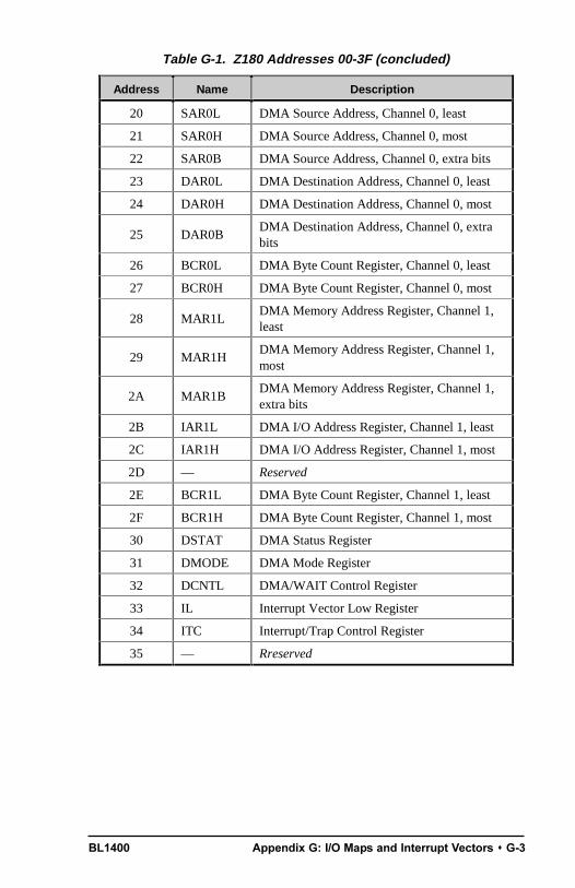
BL1400 Appendix G: I/O Maps and Interrupt Vectors s G-3
Table G-1. Z180 Addresses 00-3F (concluded)
Address Name Description
20 SAR0L DMA Source Address, Channel 0, least
21 SAR0H DMA Source Address, Channel 0, most
22 SAR0B DMA Source Address, Channel 0, extra bits
23 DAR0L DMA Destination Address, Channel 0, least
24 DAR0H DMA Destination Address, Channel 0, most
25 DAR0BDMA Destination Address, Channel 0, extrabits
26 BCR0L DMA Byte Count Register, Channel 0, least
27 BCR0H DMA Byte Count Register, Channel 0, most
28 MAR1LDMA Memory Address Register, Channel 1,least
29 MAR1HDMA Memory Address Register, Channel 1,most
2A MAR1BDMA Memory Address Register, Channel 1,extra bits
2B IAR1L DMA I/O Address Register, Channel 1, least
2C IAR1H DMA I/O Address Register, Channel 1, most
2D — Reserved
2E BCR1L DMA Byte Count Register, Channel 1, least
2F BCR1H DMA Byte Count Register, Channel 1, most
30 DSTAT DMA Status Register
31 DMODE DMA Mode Register
32 DCNTL DMA/WAIT Control Register
33 IL Interrupt Vector Low Register
34 ITC Interrupt/Trap Control Register
35 — Rreserved
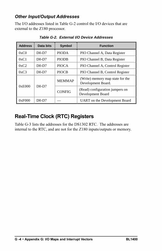
BL1400G -4 s Appendix G: I/O Maps and Interrupt Vectors
Other Input/Output Addresses
The I/O addresses listed in Table G-2 control the I/O devices that areexternal to the Z180 processor.
Table G-2. External I/O Device Addresses
Address Data bits Symbol Function
0xC0 D0-D7 PIODA PIO Channel A, Data Register
0xC1 D0-D7 PIODB PIO Channel B, Data Register
0xC2 D0-D7 PIOCA PIO Channel A, Control Register
0xC3 D0-D7 PIOCB PIO Channel B, Control Register
MEMMAP (Write) memory map state for the Development Board.
0xE000 D0-D7
CONFIG(Read) configuration jumpers onDevelopment Board
0xF000 D0-D7 — UART on the Development Board
Real-Time Clock (RTC) RegistersTable G-3 lists the addresses for the DS1302 RTC. The addresses areinternal to the RTC, and are not for the Z180 inputs/outputs or memory.
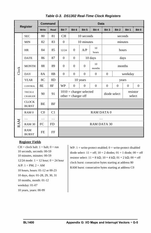
BL1400 Appendix G: I/O Maps and Interrupt Vectors s G-5
Table G-3. DS1302 Real-Time Clock Registers
Command DataRegister
Write Read Bit 7 Bit 6 Bit 5 Bit 4 Bit 3 Bit 2 Bit 1 Bit 0
SEC 80 81 CH 10 seconds seconds
MIN 82 83 0 10 minutes minutes
HR 84 85 12/24 0 A/P10
hourshours
DATE 86 87 0 0 10 days days
MONTH 88 89 0 0 010
monthsmonths
DAY 8A 8B 0 0 0 0 0 weekday
YEAR 8C 8D 10 years years
CONTROL 8E 8F WP 0 0 0 0 0 0 0
TRICKLE
CHARGER90 91
1010 = charger selectedother = charger off
diode selectresistorselect
Clo
ck
CLOCKBURST
BE BF
RAM 0 C0 C1 RAM DATA 0
… … … …
RAM 30 FC FD RAM DATA 30
RA
M
RAMBURST
FE FF
Register Fields
CH = clock halt: 1 = halt; 0 = run
10 seconds, seconds: 00-5910 minutes, minutes: 00-59
12/24 mode: 1 = 12 hour; 0 = 24 hour
A/P: 1 = PM; 2 = AM
10 hours, hours: 01-12 or 00-23
10 days, days: 01-28, 29, 30, 31
10 months, month: 01-12
weekday: 01-07
10 years, years: 00-99
WP: 1 = write-protect enabled; 0 = write-protect disabled
diode select: 11 = off; 10 = 2 diodes; 01 = 1 diode; 00 = off
resistor select: 11 = 8 kΩ; 10 = 4 kΩ; 01 = 2 kΩ; 00 = off
clock burst: consecutive bytes starting at address 80
RAM burst: consecutive bytes starting at address C0

BL1400G -6 s Appendix G: I/O Maps and Interrupt Vectors
Table G-4. Interrupt Vectors for Z180 Internal Devices
Address Name Description
0x00 INT1_VEC Expansion bus attention INT1 vector
0x02 INT2_VEC INT2 vector
0x04 PRT0_VEC PRT Timer Channel 0
0x06 PRT1_VEC PRT Timer Channel 1
0x08 DMA0_VEC DMA Channel 0
0x0A DMA1_VEC DMA Channel 1
0x0C CSIO_VEC Clocked Serial I/O
0x0E SER0_VEC Asynchronous Serial Port Channel 0
0x10 SER1_VEC Asynchronous Serial Port Channel 1
0x12 PIOA_VEC PIO Channel A (through INT0)
0x14 PIOB_VEC PIO Channel B (through INT0)
Interrupt VectorsTable G-4 shows a suggested interrupt vector map. Most of these inter-rupt vectors can be altered under program control. The addresses aregiven are in hex, relative to the start of the interrupt vector page, as deter-mined by the contents of the I-register. These are the default interruptvectors set by the boot code in the Dynamic C EPROM.
To vector an interrupt to a user function in Dynamic C, a directive suchas the following is used:
#INT_VEC 0x10 myfunction
The above example causes the interrupt at offset 10H (Serial Port 1 of theZ180) to invoke the function myfunction(). The function must bedeclared with the interrupt keyword.
interrupt myfunction() ...
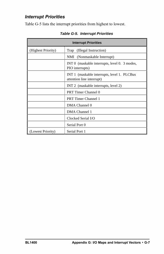
BL1400 Appendix G: I/O Maps and Interrupt Vectors s G-7
Table G-5. Interrupt Priorities
Interrupt Priorities
(Highest Priority) Trap (Illegal Instruction)
NMI (Nonmaskable Interrupt)
INT 0 (maskable interrupts, level 0. 3 modes,PIO interrupts)
INT 1 (maskable interrupts, level 1. PLCBusattention line interrupt)
INT 2 (maskable interrupts, level 2)
PRT Timer Channel 0
PRT Timer Channel 1
DMA Channel 0
DMA Channel 1
Clocked Serial I/O
Serial Port 0
(Lowest Priority) Serial Port 1
Interrupt Priorities
Table G-5 lists the interrupt priorities from highest to lowest.

BL1400G -8 s Appendix G: I/O Maps and Interrupt Vectors

BL1400 Appendix H: Simluated EEPROM s H-1
APPENDIX H: SIMULATED EEPROM
Appendix H provides information about how to use flash EPROM tosimulate EEPROM for the BL1400.
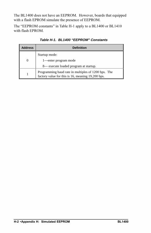
BL1400H-2 sAppendix H: Simulated EEPROM
The BL1400 does not have an EEPROM. However, boards that equippedwith a flash EPROM simulate the presence of EEPROM.
The EEPROM constants in Table H-1 apply to a BL1400 or BL1410with flash EPROM.
Table H-1. BL1400 “EEPROM” Constants
Address Definition
0
Startup mode:
1—enter program mode
8— execute loaded program at startup.
1Programming baud rate in multiples of 1200 bps. Thefactory value for this is 16, meaning 19,200 bps.

BL1400 Index s I-1
INDEX
Symbols
#define F-9#INT_VEC 4-8, 4-9, G-6+5 V C-2, D-2, D-3+5 V supply 3-14, 3-17/ASTB 3-4/AT E-3/BSTB 3-4/CTS 3-22, 3-23, 3-26/CTS/PS 3-26/CTS0 3-11/DCD0 3-21, 3-22, 3-23, 3-24/INT0 3-6/RDX E-3/RESET 3-14/RTCRST 3-15, 4-3/RTS0 3-25/RTS1 3-21/STBX E-3/WRX E-3= (assignment) A-42 × 2 LCD pinout F-44-bit bus operations E-4, E-64 × 6 keypad
initializing F-95 × 3 addressing mode E-5555 timer 1-3, 3-3, 3-15, 3-
16, 4-6, 4-7, D-6Phillips NE555D 3-17
8-bit bus operations E-4, E-5, E-79th-bit
binary communication 4-14, 4-15
transmission 3-12
A
A0X E-3A1X, A2X, A3X E-3, E-4addresses
encoding E-5
addressesmodes E-5PLCBus E-4, E-5, F-5
analog input 1-3ARDY 3-4array of pads D-3ASCI 3-23, 3-25, 3-26
channel operation 3-25Control Register A 3-25Control Register B 3-27serial ports 3-21status registers 3-23
attention line E-3
B
background routine E-6base plate 1-4, 3-14, B-6,
B-7, C-2battery
external backup 3-15, 4-5baud rate 1-5, 3-10, 3-20, 3-
21, 3-26, 3-27, 4-7, 4-9,4-14
changing 3-2Development Board
programming jumper settingsB-9
serial ports 3-21bidirectional data lines E-3BIOS
Dynamic C 1-5, 2-2, 4-3, 4-7bitwise mode
PIO 3-6, 3-7BL14_15.LIB 1-4, 4-3BL1400 1-2
block diagram 3-3default communication rate 2-8Development Board 2-2, 3-4
dimensions B-4headers and jumper settingsB-9
BL1400I-2 s Index
BL1400dimensions B-2features 1-3interfaces 3-3memory map 3-19options 1-3Prototyping Board 1-4, 2-9,
3-12, C-2, D-2, D-3,D-4, D-5dimensions B-5
BL1410features 1-3options 1-3
block diagramBL1400 3-3
BRDY 3-4buffer
receive 3-10, 3-11, 4-9,4-10, 4-14, 4-15initialization 4-9reading 4-10
transmit 3-10, 4-10, 4-15initialization 4-9writing 4-10
buscontrol registers E-7expansion 1-4, 3-10, E-2,
E-3, E-4, E-5, E-6, E-7,F-5, F-6, F-7, F-84-bit drivers E-88-bit drivers E-10addresses E-6control registers E-7devices E-6, E-7functions E-8, E-9, E-10, E-11rules for devices E-6software drivers E-7
LCD E-3operations
4-bit E-4, E-68-bit E-4, E-7
BUSADR0 E-4, E-5, F-5BUSADR1 E-4, E-5
BUSADR2 E-4, E-5, F-5BUSADR3 E-10, E-11BUSRD0 E-7, E-8, E-9,
E-11, F-5BUSRD1 E-7, E-8, F-5BUSRD2 F-5BUSWR E-8, F-5buzzer D-6BZ1 (buzzer) D-6
C
changing baud rate 3-2Charger1302 4-6charging batteries 3-15check_opto_command 4-14checking for modem commands
4-12Checksum 3-12CKA1 3-25CKA1 disable 3-25CKA1/TEND0 3-25CKA1D 3-25clock
external 3-21real-time See real-time clocktime/date 1-3, 3-6, 3-14, 3-
15, 4-3, 4-5, 4-6.clock frequency 3-10
system 3-20, 3-21, 3-26, 3-27CNTLA 3-24CNTLB 3-26CNTLB0 3-20CNTLB1 3-20COM port 1-5COMMAND mode
modem communication 3-11command protocol
master-slave 3-12common problems
programming errors A-4wrong COM port A-2
communication. See serial commu-nication

BL1400 Index s I-3
compile-time interrupt directive4-13
connectionsRS-485 two-wire network 3-13
connectors B-726-pin
pin assignments E-2Control Register A 3-25Control Register B 3-26CRC 3-12, 4-14, 4-15
computing 4-13CSIO 3-24, 4-13CTS 3-10, 3-11, 3-24, 4-9CTS Enable 3-24CTS/PS 3-26CTS1 3-24custom EPROM 2-4cyclic redundancy check 3-12,
4-14, 4-15computing 4-13
D
D0X-D7X E-3D1 D-5D2 D-5DAC board
expansion bus F-7, F-8PLCBus F-7, F-8
data format mode bits 3-25DATA mode
modem communication 3-11DB4 F-3DB5 F-3DB6 F-3DB7 F-3DC
input jack C-2, D-4unregulated input voltage B-7
DCD 3-23DCIN 2-9, 3-2, 3-14Ddelay_100ms 4-13Ddelay_1sec 4-13DebounceCount F-9, F-10
debouncing 3-14, F-9deciphering modem commands
4-12delay
in slave response 4-15modem communication 4-13
developer's kit 1-4contents 1-4, 2-2
developmentsoftware 1-5
Development Board 2-2, 3-4,B-4, B-9
headers and jumper settings B-9RAM 2-3
development methods 1-5, 2-2,2-5
Dget_modem_command 4-12digital input 1-3, 4-6digital output 1-3Dinit_z0 3-11, 4-9, 4-11DIP relays E-2disabling interrupts 4-13
DMA channels 4-13Z180 serial channels 0 and 1 4-
13disabling RS-485 driver 4-16display
liquid crystal E-3, F-3, F-8,F-9
Dkill_z0 4-10DMA 3-25DMA Channel 0
and 555 timer 4-7DMA channels
disabling interrupts 4-13downloading data 3-10, 3-11,
4-11downloading programs 4-9, 4-13DR 3-26Dread_z0 4-10Dread_z01ch 4-10DREQ0 4-7Dreset_z0rbuf 4-10Dreset_z0tbuf 4-10

BL1400I-4 s Index
Drestart_z0modem 4-12drivers
expansion bus E-74-bit E-88-bit E-10
high-level 4-3low-level 4-3relay E-7
DRIVERS.LIB E-7function library 4-16
DS1232 supervisor IC 1-3, 3-14DS1302 RTC IC 1-3, 3-15, 4-5,
4-6, G-4, G-5Dwrite_z0 4-10Dwrite_z01ch 4-10Dxmodem_z0down 4-11Dxmodem_z0up 4-11Dynamic C 1-5
BIOS 1-5, 2-2, 4-3, 4-7programming port 4-13running a sample program 2-8serial options 2-8will not start A-2
Dz0_circ_int 4-13Dz0modem_chk 4-12Dz0send_prompt 4-10
E
E000 3-5echo option 3-10, 3-11, 4-9ee_rd 4-7ee_wr 4-7EEPROM 4-13
simulated 4-7, H-2EFR 3-24
bit 3-24eioPlcAdr12 E-8eioReadD0 E-9eioReadD1 E-9eioReadD2 E-9eioResetPlcBus E-8eioWriteWR E-10EN F-3EN485 4-3
EPROM 1-3, 1-5, 2-2, 2-5,2-7, 3-4, 3-19, 4-7, 4-8, 4-9
flash 1-3, 1-5, 2-2, 2-5,4-7, H-2how to write data 4-7
jumper settings B-8escape sequences F-8Exp-A/D12 E-2expansion boards 1-4, 2-9, 3-
9, 3-14, D-2, D-3,D-4, D-5
reset E-8expansion bus 1-4, 3-10, E-2,
E-3, E-4, E-5, E-6, E-7,F-5, F-6, F-7, F-8
4-bit drivers E-88-bit drivers E-10addresses E-6devices E-6, E-7digital inputs E-7functions E-8, E-9, E-10, E-11registers E-4, E-6rules for devices E-6software drivers E-7
external battery 3-15external clock 3-21external reset switch 3-14EXTRES 3-16, D-6EZIOBL17.LIB E-7EZIOLGPL.LIB E-7EZIOMGPL.LIB E-7EZIOPL2.LIB E-7EZIOPLC.LIB E-7EZIOTGPL.LIB E-7
F
F000 3-5FE 3-24, 3-25filter
low pass D-6RC D-6
flash EPROM 1-3, 1-5, 2-2,2-5, 4-7, H-2
writing to 4-7
BL1400 Index s I-5
frequencysystem clock 3-10, 3-21,
3-26, 3-27function libraries 4-16, E-4DRIVERS.LIB 4-16PLC_EXP.LIB 4-16serial communication 4-16
G
getcrc 4-13GND 2-9, 3-2, 4-6, D-2, D-3,
F-3
H
H1 3-4, D-2, D-3H2 3-3, 3-4, 3-10, 3-12, D-3H3 2-9, 3-2, 3-3, 3-4, 3-9, 3-
10, 3-12, 3-14, 3-15, 3-16, C-2, D-2, D-3, D-4
handshakingRS-232 3-10
Hayes Smart Modem 4-12headers B-8, B-9heat dissipation
with base plate C-3without base plate C-4
heat sink 1-4, 3-14, B-6, B-7,C-2
high-level drivers 4-3hitwd 3-14
I
I/O devices G-2, G-4I/O interface 4-3I/O map G-2I/O space G-2impedance
PIO 3-4initialization
keypad F-9receive buffer 4-9
initializationserial communication 4-8transmit buffer 4-9Z180 Port 1 3-12, 4-14
initiating serial transmission4-10, 4-15
inport 3-20, E-8, E-9, E-11input mode
PIO 3-6strobed 3-6
inputsanalog 1-3, 4-6digital 1-3, 4-6, E-7RS-232 4-10
INT1 4-7, 4-13INT2 4-13interfaces 3-3
I/O 3-3interrupt handling
Z180 Port 0 4-8interrupt service functions 4-13interrupt service routines 4-13,
4-16interrupt vectors 3-21interrupt-driven driver 3-22interrupt-driven transmission 4-15interrupts 3-22, 3-23, 3-24,
E-3, E-6disabling 4-13keyword G-6PIO 3-6, 3-7, 3-8routines E-6serial 4-8
and debugging 4-8serial communication 3-10vector table 4-8, 4-13vectors G-6
J
J1 D-5J2 D-5JP4 B-9
BL1400I-6 s Index
jumper settingsBL1400 B-8
JP1 B-8JP2 B-8
BL1400 flash EPROM 2-6BL1400 non-flash EPROM 2-7Development Board 2-3, B-9Prototyping Board flash EPROM
2-6, D-3, D-5run mode B-9
K
kernelreal-time 4-13, 4-15
KEY4x6 F-9keypad 1-4keypad driver F-8, F-9
L
lc_cgram F-8lc_char F-8lc_ctrl F-8lc_init F-8lc_keyscan F-9, F-10lc_kxget F-9, F-10lc_kxinit F-9lc_printf F-8LCD 1-4, E-3, F-3, F-8, F-9
printf F-8special characters F-8
LCD bus E-3LCDX E-3LEDs D-5libraries
function 4-16, E-4communications 4-16DRIVERS.LIB 4-16PLC_EXP.LIB 4-16
liquid crystal display E-3, F-3,F-8, F-9
locationsmounting holes
base plate B-6BL1400 B-2Development Board B-4Prototyping Board B-5
low-pass filter D-6low-level drivers 4-3
M
master message format 3-12, 4-14master-slave
command protocol 3-12functional support 3-12networking 3-12, 4-16serial communication 3-12,
4-14, 4-15software support 4-14
measuring resistance 4-6memory
battery-backed 4-9extended
and uploaded data 4-11random access 3-11read only 3-4, 3-19read-only 1-3, 1-5, 2-2,
2-5, 2-7, 4-7, 4-8memory map
BL1400 3-19memory-mapped I/O register E-4mginit_dac F-7mglatch_dac1 F-7mglatch_dac2 F-7, F-8mgplc_dac_board F-7mgplc_poll_node F-6mgplc_set_relay F-6mgplcrly_board F-6mgplcuio_board F-6mgread12data0 F-5mgread12data1 F-5mgread12data2 F-5mgreset_pbus F-5mgrestore_pbus F-5, F-6mgsave_pbus F-5, F-6

BL1400 Index s I-7
mgset_dac1 F-7mgset_dac2 F-8mgset12adr F-5, F-7, F-8mgset12data F-5mgwrite_dac1 F-7mgwrite_dac2 F-7, F-8mgwrite4data F-5misticware 4-15MOD0 3-25MOD1 3-24, 3-25MOD2 3-25modes
addressing E-5PIO operation 3-5
Mode 0 3-5, 3-6Mode 1 3-5, 3-6Mode 2 3-5, 3-6Mode 3 3-5, 3-6
modems 4-9, 4-11commands 3-11, 4-12communication delay 4-13control lines 3-21deciphering commands 4-12options 3-11restarting communication 4-12
mounting holesbase plate B-6BL1400 B-2Development Board B-4Prototyping Board B-5, D-3
MP 3-26, 3-27MPBR/EFR 3-25MPBT 3-27MPE 3-26multiprocessor
bit receive/error flag reset 3-25bit transmit 3-27enable 3-26mode 3-25, 3-27
N
NE555DPhillips 3-17
networkRS-485 1-4, 3-12
network connectionstwo-wire RS-485 3-13
NO_CARRIER message 3-11nonmaskable interrupt A-3nonvolatile memory 4-7, 4-8NTC thermistors 3-18NULL modem 4-12number of bits 4-9
O
op_init_z1 4-14op_kill_z1 4-16op_rec_z1 4-15op_send_z1 4-15operating modes 4-7
PIO 3-5operating temperature B-7Opto 22 binary protocol 3-12,
4-14, 4-15, 4-16optodelay 4-15outport 3-20, 3-21, E-8,
E-9, E-11outputs
digital 1-3RS-232 3-10, 4-10
output modePIO 3-6strobed 3-6
overrun 3-24overrun error 3-24OVRN 3-24, 3-25
P
PA0 F-3PA0PA7 3-4PA1 F-3PA2 F-3PA3 F-3PA4 F-3PA5 F-3PA6 F-3
BL1400I-8 s Index
PA7 F-3parallel I/O 1-3, 3-3, 3-4, 3-5,
3-6, 3-7, F-3, F-5, F-8, F-9parity 3-26, 4-9PB0PB7 3-4PB2 3-6
and RTCDAT 3-14PB3 3-6
and RTCCLK 3-14PBUS_TG.LIB F-2PC 2-2PE 3-24, 3-25PEO 3-26Phillips NE555D 3-17phy_adr 4-11piggyback expansion boards
1-4, 3-9, 3-14, D-2,D-3, D-4, D-5
power connection 2-9PIO 1-3, 1-4, 3-3, 3-4, 3-5,
3-6, 3-7, 3-10, 4-3, F-3,F-5, F-8, F-9
bitwise mode 3-6, 3-7I/O register control word 3-7impedance 3-4interrupt control word 3-7interrupt disable word 3-8interrupt vector word 3-7interrupts 3-6mask control word 3-8Mode 0 3-5, 3-6Mode 1 3-5, 3-6Mode 2 3-5, 3-6Mode 3 3-5, 3-6, 3-7mode control word 3-7operation modes 3-5ports 4-3Port A 3-4, 3-5, 3-7, 4-3,
F-5, F-8, F-9Port B 3-4, 3-5, 3-6, 3-7, 4-3,
F-9registers 3-5strobed input mode 3-6strobed output mode 3-6
PIOA_VEC 3-7PIOB_VEC 3-7PIOCA 4-4PIOCAShadow 4-3, 4-4PIOCB 4-4PIOCBShadow 4-3, 4-4PIODA 4-4PIODB 4-4, 4-5PLC_EXP.LIB
function library 4-16PLCBus 3-10, E-2, E-3, E-4,
E-5, E-6, E-7, F-526-pin connector
pin assignments E-24-bit operations E-4, E-58-bit operations E-4, E-5addresses E-4, E-5, F-5, F-
6, F-7DACs F-7, F-8installing
BL1400 F-2reading data E-4relays F-6
DIP E-2drivers E-7
reset F-5state F-6writing data E-4
portsserial 3-10, 3-11, 3-20, 3-21
asynchronous 3-21baud rate 3-21interrupt-driven 3-21multiprocessor communica-tions feature 3-21polling 3-21
power 2-9, 3-2, 3-3, 3-14,4-6, B-7, C-2, D-3, D-4
consumption 3-14maximum dissipation 3-14, C-2
power failure 1-3prescaler 3-27printf
for LCD F-8
BL1400 Index s I-9
processorstack F-6
program development methods1-5, 2-2, 2-5
via Development Board 2-2via flash EPROM 2-5via regular EPROM 2-7
programmable ROM 1-3, 1-5,2-2, 2-5, 2-7, 3-4, 3-19,4-7, 4-8, B-8
programming 1-5protocol
commandmaster-slave 3-12
Prototyping Board 1-4, 3-12,B-5, C-2, D-2, D-3,D-4, D-5
pad array D-2power rails D-2sample circuits D-5sample demonstration circuits
SW1 D-5SW2 D-5switches D-5thermistor D-6, D-7
TP1 D-5TP2 D-5TP3 D-5TP4 D-6TP5 D-6TP6 D-5TP7 D-5TP8 D-5TP9 D-6
PRT 4-13pulse-width modulation D-6PWM. See pulse-width modulation
R
RAM 4-9battery-backed 3-11BL1400 1-3, 2-2, 3-19, 4-8Development Board 2-2, 4-8
RAMscratchpad 1-3, 3-15, 4-5, 4-6static 3-11
rbuf_there 4-15RC filter D-6RDR 3-24RDRF 3-22, 3-24, 3-26RE 3-26read-only memory 1-3, 1-5, 3-4,
3-20, 4-7, 4-8, 4-9, 4-13read12data E-9Read1302 4-6read24data E-11read4data E-10Read555 4-7read8data E-11ReadBurst1302 4-6reading data on the PLCBus
E-4, E-9ReadRam1302 4-5ready line 3-4real-time clock 1-3, 3-3, 3-6,
3-14, 3-15, 4-3, 4-5,4-6, G-4
real-time kernel 4-13, 4-15receive buffer 3-10, 3-11, 4-9,
4-10, 4-14, 4-15initialization 4-9reading 4-10
receiver interrupt 3-22, 3-23,3-24
rechargeable batteries 3-15, 4-6registers
DS1302 G-5PIO 3-5real-time clock G-5Z180 I/O G-2
regulator 1-3, 3-14, C-2, D-3relays
expansion bus F-6PLCBus F-6
Reload_vec 4-8, 4-13ReplyOpto22 4-15
BL1400I-10 s Index
resetexpansion boards E-8
reset switchexternal 3-14
ResetZ180int 4-13resistance measurement 3-16,
3-17, 4-6conversion time 3-16
ResPIOCA 4-4ResPIOCB 4-4ResPIODA 4-4ResPIODB 4-5restarting modem communication
4-12RIE 3-24ROM 2-2, 2-5, 2-7
programmable 1-3, 1-5, 2-2,2-5, 2-7, 3-4, 3-19, 3-20,4-7, 4-8, 4-9, 4-13
RS F-3RS-232 communication 1-3, 2-2,
3-3, 3-9, 3-10, 3-11, 4-10handshaking 3-10serial input 4-10serial output 3-10, 4-10software support 4-9
RS-485 communication 1-3,1-4, 3-3, 3-10, 3-12, 3-13,4-14, 4-15, 4-16
disabling driver 4-16network connections 3-13
RSR 3-24RTC. See real-time clockRTCCLK 3-14, 3-15, 4-3RTCDAT 3-15, 4-3RTS 3-10, 3-11, 3-25, 4-9RTS0 3-25RUNKERNEL 4-13RXS 3-24
S
sample programs 4-16SAMPLES\BL14_15 2-8
scratchpad RAM 3-15, 4-5, 4-6SE1100 E-2select PLCBus address E-8sendOp22 4-14SER0_VEC 4-8serial communication 1-3, 1-4,
1-5, 2-2, 3-3, 3-9, 3-10,3-11, 3-12, 3-13, 3-20,3-21, 3-22, 3-23, 3-25,3-26, 3-27, 4-8, 4-9,4-14, 4-15
establishing 2-8function libraries 4-16initialization routines 4-8interrupts 3-10master-slave 3-12, 4-14, 4-15RS-232 1-3, 2-2, 3-3, 3-9,
3-10, 3-11, 4-9, 4-10RS-485 1-3, 1-4, 3-3, 3-10,
3-12, 3-13, 4-14, 4-15, 4-16RS-485 network 3-12
serial interrupts 4-8and debugging 4-8
serial ports 3-10, 3-11, 3-20,3-21
asynchronous 3-21baud rate 3-21interrupt-driven 3-21low-level utility functions 3-20multiprocessor communications
feature 3-21polling 3-21
serial transmissioninitiating 4-10terminating 4-10
set12adr E-8set16adr E-8set24adr E-10set4adr E-9Set555 4-7set8adr E-11setPIOCA 4-4setPIOCB 4-4setPIODA 4-4
BL1400 Index s I-11
setPIODB 4-4shadow registers E-6simulated EEPROM H-2slave response delay 4-15slave response format 3-12, 4-15SmartModem
Hayes 4-12software development 1-5software development methods
1-5, 2-2, 2-5software libraries 4-16, E-4source (C term) A-4special characters
for LCD F-8specifcations
general B-3SS 3-26SS0 3-26SS1 3-26SS2 3-26stack
processor F-6STAT0 3-23static RAM 3-11stop bits 4-9storage temperature B-7strobed input mode
PIO 3-6strobed output mode
PIO 3-6struct tm 4-5super capacitors 3-15, 4-6supervisor IC 1-3, 3-14support libraries 4-16suspend 4-13, 4-15switch
external reset 3-14sysclock 3-20system clock frequency 3-10,
3-20, 3-21, 3-26, 3-27
T
TDR 3-25TDRE 3-22, 3-23, 3-25TE 3-25temperature
operating B-7storage B-7
temperatuve vs resistance inthermistors 3-18
termination resistors 3-13test pads D-3thermistors
NTC 3-18temperatuve vs. resistance 3-18
TIE 3-22, 3-23time and date
structure 4-5time/date clock 1-3, 3-3, 3-6,
3-14, 3-15, 4-3, 4-5, 4-6timer
555 1-3, 3-15, 3-16, 4-6, 4-7PRT 4-13watchdog 1-3, 3-14
tm 4-5tm_rd 4-5tm_wr 4-5TMRD0L 4-7transmission
initiating 4-10, 4-15interrupt-driven 4-15
transmit buffer 3-10, 4-10, 4-15initialization 4-9writing 4-10
trickle charge timekeeper 4-5trickle charger 4-6troubleshooting
baud rate A-2C will not start A-2cables A-2com port A-3communication mode A-2expansion boards A-2input/output problems A-3
BL1400I-12 s Index
troubleshootingmemory size A-3nonmaskable interrupts A-3operating mode A-3power supply A-3repeated interrupts A-3serial link A-3watchdog timer A-3
two-wire connectionsRS-485 network 3-13
U
U1 3-4U10 3-10U11 3-10U2 3-14U3 3-14U6 3-4U8 3-16U9 3-15UART 3-5UIO board
expansion bus F-6PLCBus F-6
unregulated input voltage B-7uploading data 3-10, 3-11, 4-11
V
VBAT 3-15, 4-6VCC 3-4, 3-14, F-3VO F-3VSS F-3
W
watchdog timer 1-3, 3-14, A-3write12data E-10Write1302 4-6write24data E-11write4data E-10write8data E-11WriteBurst1302 4-6WriteFlash 4-7, 4-8WriteRam1302 4-5
writing data on the PLCBusE-4, E-10
X
X7R 3-17xdata 4-7, 4-11XMODEM commands 4-11XMODEM protocol 3-10,
3-11, 4-11XP8100 E-2XP8200 E-2, F-6XP8300 E-2, F-6XP8400 E-2, F-6XP8500 E-2XP8600 E-2XP8700 E-2, E-4, E-7XP8800 E-2, E-7XP8900 E-2
Z
z0binaryreset 4-10z0binaryset 4-11z0modemset 4-11z0modemstat 4-11z1_op_int 4-16Z180
I/O registers G-2Microprocessor Family User's
Manual 3-20MPU User's Manual 3-20Port 0 3-11, 4-9, 4-10, 4-11,
4-13interrupt handling 4-8
Port 1 3-12, 4-16, G-6initialization 3-12, 4-14
Serial Channel 0 3-21Serial Channel 1 3-21Serial Channels 0 and 1
disabling interrupts 4-13Z180baud 3-20Z80 Microprocessor Family
Manual 3-7

Part No. 019-0017-02Revision 2
Printed in U.S.A.
Z-World2900 Spafford Street
Davis, California 95616-6800 USA
Telephone:Facsimile:
24-Hour FaxBack:Web Site:
E-Mail:
(530) 757-3737(530) 753-5141(530) 753-0618http://www.z [email protected]