bk1 - rutgers eceorfanidi/ewa/ch14.pdf14 s-parameters 14.1 scattering parameters linear two-port...
TRANSCRIPT

14S-Parameters
14.1 Scattering Parameters
Linear two-port (and multi-port) networks are characterized by a number of equivalentcircuit parameters, such as their transfer matrix, impedance matrix, admittance matrix,and scattering matrix. Fig. 14.1.1 shows a typical two-port network.
Fig. 14.1.1 Two-port network.
The transfer matrix, also known as the ABCD matrix, relates the voltage and currentat port 1 to those at port 2, whereas the impedance matrix relates the two voltagesV1, V2 to the two currents I1, I2:†[
V1
I1
]=
[A BC D
][V2
I2
](transfer matrix)
[V1
V2
]=
[Z11 Z12
Z21 Z22
][I1
−I2
](impedance matrix)
(14.1.1)
Thus, the transfer and impedance matrices are the 2×2 matrices:
T =[A BC D
], Z =
[Z11 Z12
Z21 Z22
](14.1.2)
The admittance matrix is simply the inverse of the impedance matrix, Y = Z−1. Thescattering matrix relates the outgoing waves b1, b2 to the incoming waves a1, a2 thatare incident on the two-port:
†In the figure, I2 flows out of port 2, and hence −I2 flows into it. In the usual convention, both currentsI1, I2 are taken to flow into their respective ports.
664 14. S-Parameters
[b1
b2
]=
[S11 S12
S21 S22
][a1
a2
], S =
[S11 S12
S21 S22
](scattering matrix) (14.1.3)
The matrix elements S11, S12, S21, S22 are referred to as the scattering parameters orthe S-parameters. The parameters S11, S22 have the meaning of reflection coefficients,and S21, S12, the meaning of transmission coefficients.
The many properties and uses of the S-parameters in applications are discussedin [1135–1174]. One particularly nice overview is the HP application note AN-95-1 byAnderson [1150] and is available on the web [1847].
We have already seen several examples of transfer, impedance, and scattering ma-trices. Eq. (11.7.6) or (11.7.7) is an example of a transfer matrix and (11.8.1) is thecorresponding impedance matrix. The transfer and scattering matrices of multilayerstructures, Eqs. (6.6.23) and (6.6.37), are more complicated examples.
The traveling wave variables a1, b1 at port 1 and a2, b2 at port 2 are defined in termsof V1, I1 and V2, I2 and a real-valued positive reference impedance Z0 as follows:
a1 = V1 + Z0I1
2√Z0
b1 = V1 − Z0I1
2√Z0
a2 = V2 − Z0I2
2√Z0
b2 = V2 + Z0I2
2√Z0
(traveling waves) (14.1.4)
The definitions at port 2 appear different from those at port 1, but they are reallythe same if expressed in terms of the incoming current −I2:
a2 = V2 − Z0I2
2√Z0
= V2 + Z0(−I2)2√Z0
b2 = V2 + Z0I2
2√Z0
= V2 − Z0(−I2)2√Z0
The term traveling waves is justified below. Eqs. (14.1.4) may be inverted to expressthe voltages and currents in terms of the wave variables:
V1 =√Z0(a1 + b1)
I1 = 1√Z0
(a1 − b1)
V2 =√Z0(a2 + b2)
I2 = 1√Z0
(b2 − a2)(14.1.5)
In practice, the reference impedance is chosen to be Z0 = 50 ohm. At lower fre-quencies the transfer and impedance matrices are commonly used, but at microwavefrequencies they become difficult to measure and therefore, the scattering matrix de-scription is preferred.
The S-parameters can be measured by embedding the two-port network (the device-under-test, or, DUT) in a transmission line whose ends are connected to a network ana-lyzer. Fig. 14.1.2 shows the experimental setup.
A typical network analyzer can measure S-parameters over a large frequency range,for example, the HP 8720D vector network analyzer covers the range from 50 MHz to

14.1. Scattering Parameters 665
40 GHz. Frequency resolution is typically 1 Hz and the results can be displayed eitheron a Smith chart or as a conventional gain versus frequency graph.
Fig. 14.1.2 Device under test connected to network analyzer.
Fig. 14.1.3 shows more details of the connection. The generator and load impedancesare configured by the network analyzer. The connections can be reversed, with thegenerator connected to port 2 and the load to port 1.
Fig. 14.1.3 Two-port network under test.
The two line segments of lengths l1, l2 are assumed to have characteristic impedanceequal to the reference impedance Z0. Then, the wave variables a1, b1 and a2, b2 arerecognized as normalized versions of forward and backward traveling waves. Indeed,according to Eq. (11.7.8), we have:
a1 = V1 + Z0I1
2√Z0
= 1√Z0
V1+
b1 = V1 − Z0I1
2√Z0
= 1√Z0
V1−
a2 = V2 − Z0I2
2√Z0
= 1√Z0
V2−
b2 = V2 + Z0I2
2√Z0
= 1√Z0
V2+
(14.1.6)
Thus, a1 is essentially the incident wave at port 1 and b1 the corresponding reflectedwave. Similarly, a2 is incident from the right onto port 2 and b2 is the reflected wavefrom port 2.
The network analyzer measures the waves a′1, b′1 and a′2, b′2 at the generator andload ends of the line segments, as shown in Fig. 14.1.3. From these, the waves at theinputs of the two-port can be determined. Assuming lossless segments and using thepropagation matrices (11.7.7), we have:
666 14. S-Parameters
[a1
b1
]=
[e−jδ1 0
0 ejδ1
][a′1b′1
],
[a2
b2
]=
[e−jδ2 0
0 ejδ2
][a′2b′2
](14.1.7)
where δ1 = βll and δ2 = βl2 are the phase lengths of the segments. Eqs. (14.1.7) can berearranged into the forms:
[b1
b2
]= D
[b′1b′2
],
[a′1a′2
]= D
[a1
a2
], D =
[ejδ1 0
0 ejδ2
]
The network analyzer measures the corresponding S-parameters of the primed vari-ables, that is,
[b′1b′2
]=
[S′11 S′12
S′21 S′22
][a′1a′2
], S′ =
[S′11 S′12
S′21 S′22
](measured S-matrix) (14.1.8)
The S-matrix of the two-port can be obtained then from:
[b1
b2
]= D
[b′1b′2
]= DS′
[a′1a′2
]= DS′D
[a1
a2
]⇒ S = DS′D
or, more explicitly,
[S11 S12
S21 S22
]=
[ejδ1 0
0 ejδ2
][S′11 S′12
S′21 S′22
][ejδ1 0
0 ejδ2
]
=[S′11e2jδ1 S′12ej(δ1+δ2)
S′21ej(δ1+δ2) S′22e2jδ2
] (14.1.9)
Thus, changing the points along the transmission lines at which the S-parametersare measured introduces only phase changes in the parameters.
Without loss of generality, we may replace the extended circuit of Fig. 14.1.3 with theone shown in Fig. 14.1.4 with the understanding that either we are using the extendedtwo-port parameters S′, or, equivalently, the generator and segment l1 have been re-placed by their Thevenin equivalents, and the load impedance has been replaced by itspropagated version to distance l2.
Fig. 14.1.4 Two-port network connected to generator and load.

14.2. Power Flow 667
The actual measurements of the S-parameters are made by connecting to a matchedload, ZL = Z0. Then, there will be no reflected waves from the load, a2 = 0, and theS-matrix equations will give:
b1 = S11a1 + S12a2 = S11a1 ⇒ S11 = b1
a1
∣∣∣∣ZL=Z0
= reflection coefficient
b2 = S21a1 + S22a2 = S21a1 ⇒ S21 = b2
a1
∣∣∣∣ZL=Z0
= transmission coefficient
Reversing the roles of the generator and load, one can measure in the same way theparameters S12 and S22.
14.2 Power Flow
Power flow into and out of the two-port is expressed very simply in terms of the travelingwave amplitudes. Using the inverse relationships (14.1.5), we find:
1
2Re[V∗1 I1] = 1
2|a1|2 − 1
2|b1|2
−1
2Re[V∗2 I2] = 1
2|a2|2 − 1
2|b2|2
(14.2.1)
The left-hand sides represent the power flow into ports 1 and 2. The right-hand sidesrepresent the difference between the power incident on a port and the power reflectedfrom it. The quantity Re[V∗2 I2]/2 represents the power transferred to the load.
Another way of phrasing these is to say that part of the incident power on a portgets reflected and part enters the port:
1
2|a1|2 = 1
2|b1|2 + 1
2Re[V∗1 I1]
1
2|a2|2 = 1
2|b2|2 + 1
2Re[V∗2 (−I2)]
(14.2.2)
One of the reasons for normalizing the traveling wave amplitudes by√Z0 in the
definitions (14.1.4) was precisely this simple way of expressing the incident and reflectedpowers from a port.
If the two-port is lossy, the power lost in it will be the difference between the powerentering port 1 and the power leaving port 2, that is,
Ploss = 1
2Re[V∗1 I1]−1
2Re[V∗2 I2]= 1
2|a1|2 + 1
2|a2|2 − 1
2|b1|2 − 1
2|b2|2
Noting that a†a = |a1|2 + |a2|2 and b†b = |b1|2 + |b2|2, and writing b†b = a†S†Sa,we may express this relationship in terms of the scattering matrix:
Ploss = 1
2a†a− 1
2b†b = 1
2a†a− 1
2a†S†Sa = 1
2a†(I − S†S)a (14.2.3)
668 14. S-Parameters
For a lossy two-port, the power loss is positive, which implies that the matrix I−S†Smust be positive definite. If the two-port is lossless, Ploss = 0, the S-matrix will beunitary, that is, S†S = I.
We already saw examples of such unitary scattering matrices in the cases of the equaltravel-time multilayer dielectric structures and their equivalent quarter wavelength mul-tisection transformers.
14.3 Parameter Conversions
It is straightforward to derive the relationships that allow one to pass from one param-eter set to another. For example, starting with the transfer matrix, we have:
V1 = AV2 + BI2
I1 = CV2 +DI2
⇒V1 = A
( 1
CI1 − D
CI2)+ BI2 = A
CI1 − AD− BC
CI2
V2 = 1
CI1 − D
CI2
The coefficients of I1, I2 are the impedance matrix elements. The steps are reversible,and we summarize the final relationships below:
Z =[Z11 Z12
Z21 Z22
]= 1
C
[A AD− BC1 D
]
T =[A BC D
]= 1
Z21
[Z11 Z11Z22 − Z12Z21
1 Z22
] (14.3.1)
We note the determinants det(T)= AD − BC and det(Z)= Z11Z22 − Z12Z21. Therelationship between the scattering and impedance matrices is also straightforward toderive. We define the 2×1 vectors:
V =[V1
V2
], I =
[I1
−I2
], a =
[a1
a2
], b =
[b1
b2
](14.3.2)
Then, the definitions (14.1.4) can be written compactly as:
a = 1
2√Z0
(V+ Z0I)= 1
2√Z0
(Z + Z0I)I
b = 1
2√Z0
(V− Z0I)= 1
2√Z0
(Z − Z0I)I(14.3.3)
where we used the impedance matrix relationship V = ZI and defined the 2×2 unitmatrix I. It follows then,
1
2√Z0
I = (Z + Z0I)−1a ⇒ b = 1
2√Z0
(Z − Z0I)I = (Z − Z0I)(Z + Z0I)−1a
Thus, the scattering matrix S will be related to the impedance matrix Z by
S = (Z − Z0I)(Z + Z0I)−1 � Z = (I − S)−1(I + S)Z0 (14.3.4)

14.4. Input and Output Reflection Coefficients 669
Explicitly, we have:
S =[Z11 − Z0 Z12
Z21 Z22 − Z0
][Z11 + Z0 Z12
Z21 Z22 + Z0
]−1
=[Z11 − Z0 Z12
Z21 Z22 − Z0
]1
Dz
[Z22 + Z0 −Z12
−Z21 Z11 + Z0
]
where Dz = det(Z + Z0I)= (Z11 + Z0)(Z22 + Z0)−Z12Z21. Multiplying the matrixfactors, we obtain:
S = 1
Dz
[(Z11 − Z0)(Z22 + Z0)−Z12Z21 2Z12Z0
2Z21Z0 (Z11 + Z0)(Z22 − Z0)−Z12Z21
](14.3.5)
Similarly, the inverse relationship gives:
Z = Z0
Ds
[(1+ S11)(1− S22)+S12S21 2S12
2S21 (1− S11)(1+ S22)+S12S21
](14.3.6)
where Ds = det(I− S)= (1− S11)(1− S22)−S12S21. Expressing the impedance param-eters in terms of the transfer matrix parameters, we also find:
S = 1
Da
⎡⎢⎢⎣A+ B
Z0−CZ0 −D 2(AD− BC)
2 −A+ BZ0−CZ0 +D
⎤⎥⎥⎦ (14.3.7)
where Da = A+ BZ0+CZ0 +D.
14.4 Input and Output Reflection Coefficients
When the two-port is connected to a generator and load as in Fig. 14.1.4, the impedanceand scattering matrix equations take the simpler forms:
V1 = ZinI1
V2 = ZLI2
�b1 = Γina1
a2 = ΓLb2
(14.4.1)
where Zin is the input impedance at port 1, and Γin, ΓL are the reflection coefficients atport 1 and at the load:
Γin = Zin − Z0
Zin + Z0, ΓL = ZL − Z0
ZL + Z0(14.4.2)
The input impedance and input reflection coefficient can be expressed in terms ofthe Z- and S-parameters, as follows:
670 14. S-Parameters
Zin = Z11 − Z12Z21
Z22 + ZL� Γin = S11 + S12S21ΓL
1− S22ΓL(14.4.3)
The equivalence of these two expressions can be shown by using the parameterconversion formulas of Eqs. (14.3.5) and (14.3.6), or they can be shown indirectly, asfollows. Starting with V2 = ZLI2 and using the second impedance matrix equation, wecan solve for I2 in terms of I1:
V2 = Z21I1 − Z22I2 = ZLI2 ⇒ I2 = Z21
Z22 + ZLI1 (14.4.4)
Then, the first impedance matrix equation implies:
V1 = Z11I1 − Z12I2 =(Z11 − Z12Z21
Z22 + ZL
)I1 = ZinI1
Starting again with V2 = ZLI2 we find for the traveling waves at port 2:
a2 = V2 − Z0I2
2√Z0
= ZL − Z0
2√Z0
I2
b2 = V2 + Z0I2
2√Z0
= ZL + Z0
2√Z0
I2
⇒ a2 = ZL − Z0
ZL + Z0b2 = ΓLb2
Using V1 = ZinI1, a similar argument implies for the waves at port 1:
a1 = V1 + Z0I1
2√Z0
= Zin + Z0
2√Z0
I1
b1 = V1 − Z0I1
2√Z0
= Zin − Z0
2√Z0
I1
⇒ b1 = Zin − Z0
Zin + Z0a1 = Γina1
It follows then from the scattering matrix equations that:
b2 = S21a1 + S22a2 = S22a1 + S22ΓLb2 ⇒ b2 = S21
1− S22ΓLa1 (14.4.5)
which implies for b1:
b1 = S11a1 + S12a2 = S11a1 + S12ΓLb2 =(S11 + S12S21ΓL
1− S22ΓL
)a1 = Γina1
Reversing the roles of generator and load, we obtain the impedance and reflectioncoefficients from the output side of the two-port:
Zout = Z22 − Z12Z21
Z11 + ZG� Γout = S22 + S12S21ΓG
1− S11ΓG(14.4.6)
where
Γout = Zout − Z0
Zout + Z0, ΓG = ZG − Z0
ZG + Z0(14.4.7)
14.5. Stability Circles 671
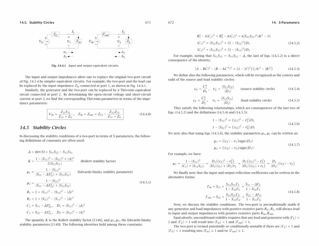
Fig. 14.4.1 Input and output equivalent circuits.
The input and output impedances allow one to replace the original two-port circuitof Fig. 14.1.4 by simpler equivalent circuits. For example, the two-port and the load canbe replaced by the input impedance Zin connected at port 1, as shown in Fig. 14.4.1.
Similarly, the generator and the two-port can be replaced by a Thevenin equivalentcircuit connected at port 2. By determining the open-circuit voltage and short-circuitcurrent at port 2, we find the corresponding Thevenin parameters in terms of the impe-dance parameters:
Vth = Z21VG
Z11 + ZG, Zth = Zout = Z22 − Z12Z21
Z11 + ZG(14.4.8)
14.5 Stability Circles
In discussing the stability conditions of a two-port in terms of S-parameters, the follow-ing definitions of constants are often used:
Δ = det(S)= S11S22 − S12S21
K = 1− |S11|2 − |S22|2 + |Δ|22|S12S21| (Rollett stability factor)
μ1 = 1− |S11|2|S22 −ΔS∗11| + |S12S21| (Edwards-Sinsky stability parameter)
μ2 = 1− |S22|2|S11 −ΔS∗22| + |S12S21|
B1 = 1+ |S11|2 − |S22|2 − |Δ|2
B2 = 1+ |S22|2 − |S11|2 − |Δ|2
C1 = S11 −ΔS∗22 , D1 = |S11|2 − |Δ|2
C2 = S22 −ΔS∗11 , D2 = |S22|2 − |Δ|2
(14.5.1)
The quantity K is the Rollett stability factor [1146], and μ1, μ2, the Edwards-Sinskystability parameters [1149]. The following identities hold among these constants:
672 14. S-Parameters
B21 − 4|C1|2 = B2
2 − 4|C2|2 = 4|S12S21|2(K2 − 1)
|C1|2 = |S12S21|2 +(1− |S22|2
)D1
|C2|2 = |S12S21|2 +(1− |S11|2
)D2
(14.5.2)
For example, noting that S12S21 = S11S22 − Δ, the last of Eqs. (14.5.2) is a directconsequence of the identity:
|A− BC|2 − |B−AC∗|2 = (1− |C|2)(|A|2 − |B|2) (14.5.3)
We define also the following parameters, which will be recognized as the centers andradii of the source and load stability circles:
cG = C∗1D1
, rG = |S12S21||D1| (source stability circle) (14.5.4)
cL = C∗2D2
, rL = |S12S21||D2| (load stability circle) (14.5.5)
They satisfy the following relationships, which are consequences of the last two ofEqs. (14.5.2) and the definitions (14.5.4) and (14.5.5):
1− |S11|2 =(|cL|2 − r2
L)D2
1− |S22|2 =(|cG|2 − r2
G)D1
(14.5.6)
We note also that using Eqs. (14.5.6), the stability parameters μ1, μ2 can be written as:
μ1 =(|cL| − rL
)sign(D2)
μ2 =(|cG| − rG
)sign(D1)
(14.5.7)
For example, we have:
μ1 = 1− |S11|2|C2| + |S12S21| =
D2(|cL|2 − r2
L)
|D2||cL| + |D2|rL =D2
(|cL|2 − r2L)
|D2|(|cL| + rL
) = D2
|D2|(|cL| − rL
)
We finally note that the input and output reflection coefficients can be written in thealternative forms:
Γin = S11 + S12S21ΓL1− S22ΓL
= S11 −ΔΓL1− S22ΓL
Γout = S22 + S12S21ΓG1− S22ΓG
= S22 −ΔΓG1− S11ΓG
(14.5.8)
Next, we discuss the stability conditions. The two-port is unconditionally stable ifany generator and load impedances with positive resistive parts RG,RL, will always leadto input and output impedances with positive resistive parts Rin, Rout.
Equivalently, unconditional stability requires that any load and generator with |ΓL| <1 and |ΓG| < 1 will result into |Γin| < 1 and |Γout| < 1.
The two-port is termed potentially or conditionally unstable if there are |ΓL| < 1 and|ΓG| < 1 resulting into |Γin| ≥ 1 and/or |Γout| ≥ 1.

14.5. Stability Circles 673
The load stability region is the set of all ΓL that result into |Γin| < 1, and the sourcestability region, the set of all ΓG that result into |Γout| < 1.
In the unconditionally stable case, the load and source stability regions contain theentire unit-circles |ΓL| < 1 or |ΓG| < 1. However, in the potentially unstable case, onlyportions of the unit-circles may lie within the stability regions and such ΓG, ΓL will leadto a stable input and output impedances.
The connection of the stability regions to the stability circles is brought about by thefollowing identities, which can be proved easily using Eqs. (14.5.1)–(14.5.8):
1− |Γin|2 = |ΓL − cL|2 − r2L
|1− S22ΓL|2 D2
1− |Γout|2 = |ΓG − cG|2 − r2G
|1− S11ΓG|2 D1
(14.5.9)
For example, the first can be shown starting with Eq. (14.5.8) and using the definitions(14.5.5) and the relationship (14.5.6):
1− |Γin|2 = 1−∣∣∣∣S11 −ΔΓL
1− S22ΓL
∣∣∣∣2
= |S11 −ΔΓL|2 − |1− S22ΓL|2|1− S22ΓL|2
=(|S22|2 − |Δ|2
)|ΓL|2 − (S22 −ΔS∗11)ΓL − (S∗22 −Δ∗S11)Γ∗L + 1− |S11|2|1− S22ΓL|2
= D2|ΓL|2 −C2ΓL −C∗2 Γ∗L + 1− |S11|2|1− S22ΓL|2
= D2(|ΓL|2 − c∗LΓL − c∗LΓ
∗L + |cL|2 − r2
L)
|1− S22ΓL|2 = D2(|ΓL − cL|2 − r2
L)
|1− S22ΓL|2
It follows from Eq. (14.5.9) that the load stability region is defined by the conditions:
1− |Γin|2 > 0 �(|ΓL − cL|2 − r2
L)D2 > 0
Depending on the sign of D2, these are equivalent to the outside or the inside of theload stability circle of center cL and radius rL:
|ΓL − cL| > rL , if D2 > 0
|ΓL − cL| < rL , if D2 < 0(load stability region) (14.5.10)
The boundary of the circle |ΓL−cL| = rL corresponds to |Γin| = 1. The complementof these regions corresponds to the unstable region with |Γin| > 1. Similarly, we findfor the source stability region:
|ΓG − cG| > rG , if D1 > 0
|ΓG − cG| < rG , if D1 < 0(source stability region) (14.5.11)
In order to have unconditional stability, the stability regions must contain the unit-circle in its entirety. If D2 > 0, the unit-circle and load stability circle must not overlap
674 14. S-Parameters
at all, as shown in Fig. 14.5.1. Geometrically, the distance between the pointsO andA inthe figure is (OA)= |cL|−rL. The non-overlapping of the circles requires the condition(OA)> 1, or, |cL| − rL > 1.
If D2 < 0, the stability region is the inside of the stability circle, and therefore, theunit-circle must lie within that circle. This requires that (OA)= rL−|cL| > 1, as shownin Fig. 14.5.1.
Fig. 14.5.1 Load stability regions in the unconditionally stable case.
These two conditions can be combined into sign(D2)(|cL| − rL
)> 1. But, that is
equivalent to μ1 > 1 according to Eq. (14.5.7). Geometrically, the parameter μ1 repre-sents the distance (OA). Thus, the condition for the unconditional stability of the inputis equivalent to:
μ1 > 1 (unconditional stability condition) (14.5.12)
It has been shown by Edwards and Sinsky [1149] that this single condition (or, alter-natively, the single condition μ2 > 1) is necessary and sufficient for the unconditionalstability of both the input and output impedances of the two-port. Clearly, the sourcestability regions will be similar to those of Fig. 14.5.1.
If the stability condition is not satisfied, that is, μ1 < 1, then only that portion of theunit-circle that lies within the stability region will be stable and will lead to stable inputand output impedances. Fig. 14.5.2 illustrates such a potentially unstable case.
If D2 > 0, then μ1 < 1 is equivalent to |cL| − rL < 1, and if D2 < 0, it is equivalentto rL − |cL| < 1. In either case, the unit-circle is partially overlapping with the stabilitycircle, as shown in Fig. 14.5.2. The portion of the unit-circle that does not lie within thestability region will correspond to an unstable Zin.
There exist several other unconditional stability criteria that are equivalent to thesingle criterion μ1 > 1. They all require that the Rollett stability factor K be greaterthan unity, K > 1, as well as one other condition. Any one of the following criteria arenecessary and sufficient for unconditional stability [1147]:

14.5. Stability Circles 675
Fig. 14.5.2 Load stability regions in potentially unstable case.
K > 1 and |Δ| < 1K > 1 and B1 > 0K > 1 and B2 > 0K > 1 and |S12S21| < 1− |S11|2K > 1 and |S12S21| < 1− |S22|2
(stability conditions) (14.5.13)
Their equivalence to μ1 > 1 has been shown in [1149]. In particular, it follows fromthe last two conditions that unconditional stability requires |S11| < 1 and |S22| < 1.These are necessary but not sufficient for stability.
A very common circumstance in practice is to have a potentially unstable two-port,but with |S11| < 1 and |S22| < 1. In such cases, Eq. (14.5.6) implies D2
(|cL|2 − r2L)> 0,
and the lack of stability requires μ1 = sign(D2)(|cL|2 − r2
L)< 1.Therefore, if D2 > 0, then we must have |cL|2 − r2
L > 0 and |cL| − rL < 1, whichcombine into the inequality rL < |cL| < rL + 1. This is depicted in the left picture ofFig. 14.5.2. The geometrical distance (OA)= |cL| − rL satisfies 0 < (OA)< 1, so thatstability circle partially overlaps with the unit-circle but does not enclose its center.
On the other hand, ifD2 < 0, the two conditions require |cL|2−r2L < 0 and rL−|cL| <
1, which imply |cL| < rL < |cL| + 1. This is depicted in the right Fig. 14.5.2. Thegeometrical distance (OA)= rL − |cL| again satisfies 0 < (OA)< 1, but now the centerof the unit-circle lies within the stability circle, which is also the stability region.
We have written a number of MATLAB functions that facilitate working with S-parameters. They are described in detail later on:
smat reshape S-parameters into S-matrix
sparam calculate stability parameters
sgain calculate transducer, available, operating, and unilateral power gains
smatch calculate simultaneous conjugate match for generator and load
gin,gout calculate input and output reflection coefficients
smith draw a basic Smith chart
smithcir draw a stability or gain circle on Smith chart
sgcirc determine stability and gain circles
nfcirc determine noise figure circles
nfig calculate noise figure
676 14. S-Parameters
The MATLAB function sparam calculates the stability parameters μ1, K, |Δ|, B1, B2,as well as the parameters C1, C2,D1,D2. It has usage:
[K,mu,D,B1,B2,C1,C2,D1,D2] = sparam(S); % stability parameters
The function sgcirc calculates the centers and radii of the source and load stabilitycircles. It also calculates gain circles to be discussed later on. Its usage is:
[cL,rL] = sgcirc(S,’l’); % load or Zin stability circle
[cG,rG] = sgcirc(S,’s’); % source or Zout stability circle
The MATLAB function smith draws a basic Smith chart, and the function smithcirdraws the stability circles:
smith(n); % draw four basic types of Smith charts, n = 1,2,3,4
smith; % default Smith chart corresponding to n = 3
smithcir(c,r,max,width); % draw circle of center c and radius r
smithcir(c,r,max); % equivalent to linewidth width=1
smithcir(c,r); % draw full circle with linewidth width=1
The parameter max controls the portion of the stability circle that is visible outsidethe Smith chart. For example, max = 1.1 will display only that portion of the circle thathas |Γ| < 1.1.
Example 14.5.1: The Hewlett-Packard AT-41511 NPN bipolar transistor has the following S-parameters at 1 GHz and 2 GHz [1848]:
S11 = 0.48∠−149o , S21 = 5.189∠89o , S12 = 0.073∠43o , S22 = 0.49∠−39o
S11 = 0.46∠162o , S21 = 2.774∠59o , S12 = 0.103∠45o , S22 = 0.42∠−47o
Determine the stability parameters, stability circles, and stability regions.
Solution: The transistor is potentially unstable at 1 GHz, but unconditionally stable at 2 GHz.The source and load stability circles at 1 GHz are shown in Fig. 14.5.3.
Fig. 14.5.3 Load and source stability circles at 1 GHz.
The MATLAB code used to generate this graph was:

14.6. Power Gains 677
S = smat([0.48 -149 5.189 89 0.073 43 0.49 -39]); % form S-matrix
[K,mu,D,B1,B2,C1,C2,D1,D2] = sparam(S); % stability parameters
[cL,rL] = sgcirc(S,’l’); % stability circles
[cG,rG] = sgcirc(S,’s’);
smith; % draw basic Smith chart
smithcir(cL, rL, 1.1, 1.5); % draw stability circles
smithcir(cG, rG, 1.1, 1.5);
The computed stability parameters at 1 GHz were:
[K,μ1, |Δ|, B1, B2,D1,D2]= [0.781, 0.847, 0.250, 0.928, 0.947, 0.168, 0.178]
The transistor is potentially unstable because K < 1 even though |Δ| < 1, B1 > 0, andB2 > 0. The load and source stability circle centers and radii were:
cL = 2.978∠51.75o , rL = 2.131
cG = 3.098∠162.24o , rG = 2.254
Because both D1 and D2 are positive, both stability regions will be the portion of the Smithchart that lies outside the stability circles. For 2 GHz, we find:
[K,μ1, |Δ|, B1, B2,D1,D2]= [1.089, 1.056, 0.103, 1.025, 0.954, 0.201, 0.166]
cL = 2.779∠50.12o , rL = 1.723
cG = 2.473∠−159.36o , rG = 1.421
The transistor is stable at 2 GHz, with both load and source stability circles being com-pletely outside the unit-circle. ��
Problem 14.2 presents an example for which the D2 parameter is negative, so thatthe stability regions will be the insides of the stability circles. At one frequency, theunit-circle is partially overlapping with the stability circle, while at another frequency,it lies entirely within the stability circle.
14.6 Power Gains
The amplification (or attenuation) properties of the two-port can be deduced by com-paring the power Pin going into the two-port to the power PL coming out of the two-portand going into the load. These were given in Eq. (14.2.1) and we rewrite them as:
Pin = 1
2Re[V∗1 I1]= 1
2Rin|I1|2 (power into two-port)
PL = 1
2Re[V∗2 I2]= 1
2RL|I2|2 (power out of two-port and into load)
(14.6.1)
678 14. S-Parameters
where we used V1 = ZinI1, V2 = ZLI2, and defined the real parts of the input andload impedances by Rin = Re(Zin) and RL = Re(ZL). Using the equivalent circuits ofFig. 14.4.1, we may write I1, I2 in terms of the generator voltage VG and obtain:
Pin = 1
2
|VG|2Rin
|Zin + ZG|2
PL = 1
2
|Vth|2RL
|Zout + ZL|2 =1
2
|VG|2RL|Z21|2∣∣(Z11 + ZG)(Zout + ZL)∣∣2
(14.6.2)
Using the identities of Problem 14.1, PL can also be written in the alternative forms:
PL = 1
2
|VG|2RL|Z21|2∣∣(Z22 + ZL)(Zin + ZG)∣∣2 =
1
2
|VG|2RL|Z21|2∣∣(Z11 + ZG)(Z22 + ZL)−Z12Z21∣∣2 (14.6.3)
The maximum power that can be delivered by the generator to a connected loadis called the available power of the generator, PavG, and is obtained when the load isconjugate-matched to the generator, that is, PavG = Pin when Zin = Z∗G.
Similarly, the available power from the two-port network, PavN, is the maximumpower that can be delivered by the Thevenin-equivalent circuit of Fig. 14.4.1 to a con-nected load, that is, PavN = PL when ZL = Z∗th = Z∗out. It follows then from Eq. (14.6.2)that the available powers will be:
PavG = maxPin = |VG|28RG
(available power from generator)
PavN = maxPL = |Vth|28Rout
(available power from network)
(14.6.4)
Using Eq. (14.4.8), PavN can also be written as:
PavN = |VG|28Rout
∣∣∣∣ Z21
Z11 + ZG
∣∣∣∣2
(14.6.5)
The powers can be expressed completely in terms of the S-parameters of the two-port and the input and output reflection coefficients. With the help of the identities ofProblem 14.1, we find the alternative expressions for Pin and PL:
Pin = |VG|28Z0
(1− |Γin|2
)|1− ΓG|2|1− ΓinΓG|2
PL = |VG|28Z0
(1− |ΓL|2
)|1− ΓG|2|S21|2∣∣(1− ΓinΓG)(1− S22ΓL)∣∣2
= |VG|28Z0
(1− |ΓL|2
)|1− ΓG|2|S21|2∣∣(1− ΓoutΓL)(1− S11ΓG)∣∣2
= |VG|28Z0
(1− |ΓL|2
)|1− ΓG|2|S21|2∣∣(1− S11ΓG)(1− S22ΓL)−S12S21ΓGΓL∣∣2
(14.6.6)
Similarly, we have for PavG and PavN:

14.6. Power Gains 679
PavG = |VG|28Z0
|1− ΓG|21− |ΓG|2
PavN = |VG|28Z0
|1− ΓG|2|S21|2(1− |Γout|2
)|1− S11ΓG|2(14.6.7)
It is evident that PavG, PavN are obtained from Pin, PL by setting Γin = Γ∗G and ΓL =Γ∗out, which are equivalent to the conjugate-match conditions.
Three widely used definitions for the power gain of the two-port network are thetransducer power gain GT, the available power gain Ga, and the power gain Gp, alsocalled the operating gain. They are defined as follows:
GT = power out of network
maximum power in= PLPavG
(transducer power gain)
Ga = maximum power out
maximum power in= PavN
PavG(available power gain)
Gp = power out of network
power into network= PLPin
(operating power gain)
(14.6.8)
Each gain is expressible either in terms of the Z-parameters of the two-port, or interms of its S-parameters. In terms of Z-parameters, the transducer gain is given by thefollowing forms, obtained from the three forms of PL in Eqs. (14.6.2) and (14.6.3):
GT = 4RGRL|Z21|2∣∣(Z22 + ZL)(Zin + ZG)∣∣2
= 4RGRL|Z21|2∣∣(Z11 + ZG)(Zout + ZL)∣∣2
= 4RGRL|Z21|2∣∣(Z11 + ZG)(Z22 + ZL)−Z12Z21∣∣2
(14.6.9)
And, in terms of the S-parameters:
GT = 1− |ΓG|2|1− ΓinΓG|2 |S21|2 1− |ΓL|2
|1− S22ΓL|2
= 1− |ΓG|2|1− S11ΓG|2 |S21|2 1− |ΓL|2
|1− ΓoutΓL|2
= (1− |ΓG|2)|S21|2(1− |ΓL|2)∣∣(1− S11ΓG)(1− S22ΓL)−S12S21ΓGΓL∣∣2
(14.6.10)
Similarly, we have for Ga and Gp:
Ga = RG
Rout
∣∣∣∣ Z21
Z11 + ZG
∣∣∣∣2
= 1− |ΓG|2|1− S11ΓG|2 |S21|2 1
1− |Γout|2
Gp = RL
Rin
∣∣∣∣ Z21
Z22 + ZL
∣∣∣∣2
= 1
1− |Γin|2 |S21|2 1− |ΓL|2|1− S22ΓL|2
(14.6.11)
680 14. S-Parameters
The transducer gain GT is, perhaps, the most representative measure of gain forthe two-port because it incorporates the effects of both the load and generator impe-dances, whereas Ga depends only on the generator impedance and Gp only on the loadimpedance.
If the generator and load impedances are matched to the reference impedance Z0,so that ZG = ZL = Z0 and ΓG = ΓL = 0, and Γin = S11, Γout = S22, then the power gainsreduce to:
GT = |S21|2 , Ga = |S21|21− |S22|2 , Gp = |S21|2
1− |S11|2 (14.6.12)
A unilateral two-port has by definition zero reverse transmission coefficient, that is,S12 = 0. In this case, the input and output reflection coefficients simplify into:
Γin = S11 , Γout = S22 (unilateral two-port) (14.6.13)
The expressions of the power gains simplify somewhat in this case:
GTu = 1− |ΓG|2|1− S11ΓG|2 |S21|2 1− |ΓL|2
|1− S22ΓL|2
Gau = 1− |ΓG|2|1− S11ΓG|2 |S21|2 1
1− |S22|2
Gpu = 1
1− |S11|2 |S21|2 1− |ΓL|2|1− S22ΓL|2
(unilateral gains) (14.6.14)
For both the bilateral and unilateral cases, the gains Ga,Gp are obtainable from GTby setting ΓL = Γ∗out and Γin = Γ∗G, respectively, as was the case for PavN and PavG.
The relative power ratios Pin/PavG and PL/PavN measure the mismatching betweenthe generator and the two-port and between the load and the two-port. Using the defi-nitions for the power gains, we obtain the input and output mismatch factors:
Min = Pin
PavG= GT
Gp= 4RinRG
|Zin + ZG|2 =(1− |Γin|2
)(1− |ΓG|2
)|1− ΓinΓG|2 (14.6.15)
Mout = PLPavN
= GT
Ga= 4RoutRL
|Zout + ZL|2 =(1− |Γout|2
)(1− |ΓL|2
)|1− ΓoutΓL|2 (14.6.16)
The mismatch factors are always less than or equal to unity (for positive Rin andRout.) Clearly, Min = 1 under the conjugate-match condition Zin = Z∗G or Γin = Γ∗G, andMout = 1 if ZL = Z∗out or ΓL = Γ∗out. The mismatch factors can also be written in thefollowing forms, which show more explicitly the mismatch properties:
Min = 1−∣∣∣∣∣ Γin − Γ∗G
1− ΓinΓG
∣∣∣∣∣2
, Mout = 1−∣∣∣∣∣ Γout − Γ∗L
1− ΓoutΓL
∣∣∣∣∣2
(14.6.17)
These follow from the identity:
|1− Γ1Γ2|2 − |Γ1 − Γ∗2 |2 =(1− |Γ1|2
)(1− |Γ2|2
)(14.6.18)

14.6. Power Gains 681
The transducer gain is maximized when the two-port is simultaneously conjugatematched, that is, when Γin = Γ∗G and ΓL = Γ∗out. Then, Min = Mout = 1 and the threegains become equal. The common maximum gain achieved by simultaneous matchingis called the maximum available gain (MAG):
GT,max = Ga,max = Gp,max = GMAG (14.6.19)
Simultaneous matching is discussed in Sec. 14.8. The necessary and sufficient con-dition for simultaneous matching is K ≥ 1, where K is the Rollett stability factor. It canbe shown that the MAG can be expressed as:
GMAG = |S21||S12|
(K −
√K2 − 1
)(maximum available gain) (14.6.20)
The maximum stable gain (MSG) is the maximum value GMAG can have, which isachievable when K = 1:
GMSG = |S21||S12| (maximum stable gain) (14.6.21)
In the unilateral case, the MAG is obtained either by setting ΓG = Γ∗in = S∗11 andΓL = Γ∗out = S∗22 in Eq. (14.6.14), or by a careful limiting process in Eq. (14.6.20), in whichK →∞ so that both the numerator factor K−√K2 − 1 and the denominator factor |S12|tend to zero. With either method, we find the unilateral MAG:
GMAG,u = |S21|2(1− |S11|2
)(1− |S22|2
) = G1|S21|2G2 (unilateral MAG) (14.6.22)
The maximum unilateral input and output gain factors are:
G1 = 1
1− |S11|2 , G2 = 1
1− |S22|2 (14.6.23)
They are the maxima of the input and output gain factors in Eq. (14.6.14) realizedwith conjugate matching, that is, with ΓG = S∗11 and ΓL = S∗22. For any other valuesof the reflection coefficients (such that |ΓG| < 1 and ΓL| < 1), we have the followinginequalities, which follow from the identity (14.6.18):
1− |ΓG|2|1− S11ΓG|2 ≤
1
1− |S11|2 ,1− |ΓL|2|1− S22ΓL|2 ≤
1
1− |S22|2 (14.6.24)
Often two-ports, such as most microwave transistor amplifiers, are approximatelyunilateral, that is, the measured S-parameters satisfy |S12| |S21|. To decide whetherthe two-port should be treated as unilateral, a figure of merit is used, which is essentiallythe comparison of the maximum unilateral gain to the transducer gain of the actualdevice under the same matching conditions, that is, ΓG = S∗11 and ΓL = S∗22.
For these matched values ofΓG, ΓL, the ratio of the bilateral and unilateral transducergains can be shown to have the form:
gu = GT
GTu= 1
|1−U|2 , U = S12S21S∗11S∗22(
1− |S11|2)(
1− |S22|2) (14.6.25)
682 14. S-Parameters
The quantity |U| is known as the unilateral figure of merit. If the relative gain ratiogu is near unity (typically, within 10 percent of unity), the two-port may be treated asunilateral.
The MATLAB function sgain computes the transducer, available, and operatingpower gains, given the S-parameters and the reflection coefficients ΓG, ΓL. In addition,it computes the unilateral gains, the maximum available gain, and the maximum stablegain. It also computes the unilateral figure of merit ratio (14.6.25). It has usage:
Gt = sgain(S,gG,gL); transducer power gain at given ΓG,ΓLGa = sgain(S,gG,’a’); available power gain at given ΓG with ΓL = Γ∗outGp = sgain(S,gL,’p’); operating power gain at given ΓL with ΓG = Γ∗in
Gmag = sgain(S); maximum available gain (MAG)
Gmsg = sgain(S,’msg’); maximum stable gain (MSG)
Gu = sgain(S,’u’); maximum unilateral gain, Eq. (14.6.22)
G1 = sgain(S,’ui’); maximum unilateral input gain, Eq. (14.6.23)
G2 = sgain(S,’uo’); maximum unilateral output gain, Eq. (14.6.23)
gu = sgain(S,’ufm’); unilateral figure of merit gain ratio, Eq. (14.6.25)
The MATLAB functions gin and gout compute the input and output reflection coef-ficients from S and ΓG, ΓL. They have usage:
Gin = gin(S,gL); input reflection coefficient, Eq. (14.4.3)
Gout = gout(S,gG); output reflection coefficient, Eq. (14.4.6)
Example 14.6.1: A microwave transistor amplifier uses the Hewlett-Packard AT-41410 NPNbipolar transistor with the following S-parameters at 2 GHz [1848]:
S11 = 0.61∠165o , S21 = 3.72∠59o , S12 = 0.05∠42o , S22 = 0.45∠−48o
Calculate the input and output reflection coefficients and the various power gains, if theamplifier is connected to a generator and load with impedances ZG = 10− 20j and ZL =30+ 40j ohm.
Solution: The following MATLAB code will calculate all the required gains:
Z0 = 50; % normalization impedance
ZG = 10+20j; gG = z2g(ZG,Z0); % ΓG = −0.50+ 0.50j = 0.71∠135o
ZL = 30-40j; gL = z2g(ZL,Z0); % ΓL = −0.41− 0.43j = 0.59∠−133.15o
S = smat([0.61 165 3.72 59 0.05 42 0.45 -48]); % reshape S into matrix
Gin = gin(S,gL); % Γin = 0.54∠162.30o
Gout = gout(S,gG); % Γout = 0.45∠−67.46o
Gt = sgain(S,gG,gL); % GT = 4.71, or, 6.73 dB
Ga = sgain(S,gG,’a’); % Ga = 11.44, or, 10.58 dB
Gp = sgain(S,gL,’p’); % Gp = 10.51, or, 10.22 dB
Gu = sgain(S,’u’); % Gu = 27.64, or, 14.41 dB
G1 = sgain(S,’ui’); % G1 = 1.59, or, 2.02 dB
G2 = sgain(S,’uo’); % G2 = 1.25, or, 0.98 dB
14.7. Generalized S-Parameters and Power Waves 683
gu = sgain(S,’ufm’); % gu = 1.23, or, 0.89 dB
Gmag = sgain(S); % GMAG = 41.50, or, 16.18 dB
Gmsg = sgain(S,’msg’); % GMSG = 74.40, or, 18.72 dB
The amplifier cannot be considered to be unilateral as the unilateral figure of merit ratiogu = 1.23 is fairly large (larger than 10 percent from unity.)
The amplifier is operating at a gain of GT = 6.73 dB, which is far from the maximum valueof GMAG = 16.18 dB. This is because it is mismatched with the given generator and loadimpedances.
To realize the optimum gain GMAG the amplifier must ‘see’ certain optimum generatorand load impedances or reflection coefficients. These can be calculated by the MATLABfunction smatch and are found to be:
ΓG = 0.82∠−162.67o ⇒ ZG = g2z(ZG,Z0)= 5.12− 7.54j Ω
ΓL = 0.75∠52.57o ⇒ ZL = g2z(ZL,Z0)= 33.66+ 91.48j Ω
The design of such optimum matching terminations and the function smatch are discussedin Sec. 14.8. The functions g2z and z2g were discussed in Sec. 11.7 . ��
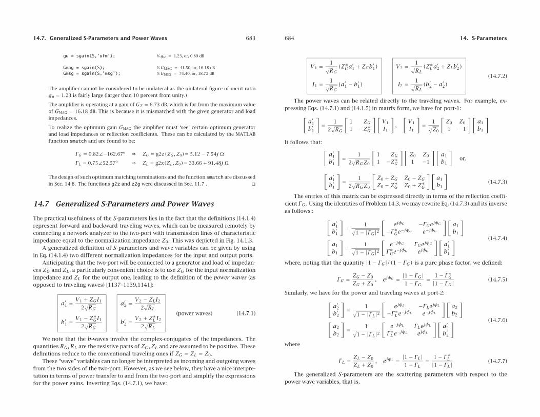
14.7 Generalized S-Parameters and Power Waves
The practical usefulness of the S-parameters lies in the fact that the definitions (14.1.4)represent forward and backward traveling waves, which can be measured remotely byconnecting a network analyzer to the two-port with transmission lines of characteristicimpedance equal to the normalization impedance Z0. This was depicted in Fig. 14.1.3.
A generalized definition of S-parameters and wave variables can be given by usingin Eq. (14.1.4) two different normalization impedances for the input and output ports.
Anticipating that the two-port will be connected to a generator and load of impedan-ces ZG and ZL, a particularly convenient choice is to use ZG for the input normalizationimpedance and ZL for the output one, leading to the definition of the power waves (asopposed to traveling waves) [1137–1139,1141]:
a′1 =V1 + ZGI1
2√RG
b′1 =V1 − Z∗GI1
2√RG
a′2 =V2 − ZLI2
2√RL
b′2 =V2 + Z∗L I2
2√RL
(power waves) (14.7.1)
We note that the b-waves involve the complex-conjugates of the impedances. Thequantities RG,RL are the resistive parts of ZG,ZL and are assumed to be positive. Thesedefinitions reduce to the conventional traveling ones if ZG = ZL = Z0.
These “wave” variables can no longer be interpreted as incoming and outgoing wavesfrom the two sides of the two-port. However, as we see below, they have a nice interpre-tation in terms of power transfer to and from the two-port and simplify the expressionsfor the power gains. Inverting Eqs. (14.7.1), we have:
684 14. S-Parameters
V1 = 1√RG
(Z∗Ga′1 + ZGb′1)
I1 = 1√RG
(a′1 − b′1)
V2 = 1√RL
(Z∗L a′2 + ZLb′2)
I2 = 1√RL
(b′2 − a′2)(14.7.2)
The power waves can be related directly to the traveling waves. For example, ex-pressing Eqs. (14.7.1) and (14.1.5) in matrix form, we have for port-1:
[a′1b′1
]= 1
2√RG
[1 ZG1 −Z∗G
][V1
I1
],
[V1
I1
]= 1√
Z0
[Z0 Z0
1 −1
][a1
b1
]
It follows that: [a′1b′1
]= 1
2√RGZ0
[1 ZG1 −Z∗G
][Z0 Z0
1 −1
][a1
b1
]or,
[a′1b′1
]= 1
2√RGZ0
[Z0 + ZG Z0 − ZGZ0 − Z∗G Z0 + Z∗G
][a1
b1
](14.7.3)
The entries of this matrix can be expressed directly in terms of the reflection coeffi-cient ΓG. Using the identities of Problem 14.3, we may rewrite Eq. (14.7.3) and its inverseas follows::
[a′1b′1
]= 1√
1− |ΓG|2[
ejφG −ΓGejφG
−Γ∗Ge−jφG e−jφG
][a1
b1
]
[a1
b1
]= 1√
1− |ΓG|2[
e−jφG ΓGejφG
Γ∗Ge−jφG ejφG
][a′1b′1
] (14.7.4)
where, noting that the quantity |1− ΓG|/(1− ΓG) is a pure phase factor, we defined:
ΓG = ZG − Z0
ZG + Z0, ejφG = |1− ΓG|
1− ΓG= 1− Γ∗G|1− ΓG| (14.7.5)
Similarly, we have for the power and traveling waves at port-2:
[a′2b′2
]= 1√
1− |ΓL|2[
ejφL −ΓLejφL
−Γ∗L e−jφL e−jφL
][a2
b2
]
[a2
b2
]= 1√
1− |ΓL|2[
e−jφL ΓLejφL
Γ∗L e−jφL ejφL
][a′2b′2
] (14.7.6)
where
ΓL = ZL − Z0
ZL + Z0, ejφL = |1− ΓL|
1− ΓL= 1− Γ∗L|1− ΓL| (14.7.7)
The generalized S-parameters are the scattering parameters with respect to thepower wave variables, that is,

14.7. Generalized S-Parameters and Power Waves 685
[b′1b′2
]=
[S′11 S′12
S′21 S′22
][a′1a′2
]⇒ b′ = S′a′ (14.7.8)
To relate S′ to the conventional scattering matrix S, we define the following diagonalmatrices:
Γ =[ΓG 00 ΓL
], F =
⎡⎢⎢⎢⎣
ejφG√1− |ΓG|2
0
0ejφL√
1− |ΓL|2
⎤⎥⎥⎥⎦ =
[FG 00 FL
](14.7.9)
Using these matrices, it follows from Eqs. (14.7.4) and (14.7.6):
a′1 = FG(a1 − ΓGb1)
a′2 = FL(a2 − ΓLb2)⇒ a′ = F(a− Γb) (14.7.10)
b′1 = F∗G(b1 − Γ∗Ga1)
b′2 = F∗L (b2 − Γ∗La2)⇒ b′ = F∗(b− Γ∗a) (14.7.11)
Using b = Sa, we find
a′ = F(a− Γb)= F(I − ΓS)a ⇒ a = (I − ΓS)−1F−1a′
b′ = F∗(S− Γ∗)a = F∗(S− Γ∗)(I − ΓS)−1F−1a′ = S′a′
where I is the 2×2 unit matrix. Thus, the generalized S-matrix is:
S′ = F∗(S− Γ∗)(I − ΓS)−1F−1 (14.7.12)
We note that S′ = S when ZG = ZL = Z0, that is, when ΓG = ΓL = 0. The explicitexpressions for the matrix elements of S′ can be derived as follows:
S′11 =(S11 − Γ∗G)(1− S22ΓL)+S21S12ΓL
(1− S11ΓG)(1− S22ΓL)−S12S21ΓGΓLe−2jφG
S′22 =(S22 − Γ∗L )(1− S11ΓG)+S21S12ΓG
(1− S11ΓG)(1− S22ΓL)−S12S21ΓGΓLe−2jφL
(14.7.13a)
S′21 =√
1− |ΓG|2 S21
√1− |ΓL|2
(1− S11ΓG)(1− S22ΓL)−S12S21ΓGΓLe−j(φG+φL)
S′12 =√
1− |ΓL|2 S12
√1− |ΓG|2
(1− S11ΓG)(1− S22ΓL)−S12S21ΓGΓLe−j(φL+φG)
(14.7.13b)
The S′11, S′22 parameters can be rewritten in terms of the input and output reflection
coefficients by using Eq. (14.13.2) and the following factorization identities:
(S11 − Γ∗G)(1− S22ΓL)+S21S12ΓL = (Γin − Γ∗G)(1− S22ΓL)(S22 − Γ∗L )(1− S11ΓG)+S21S12ΓG = (Γout − Γ∗L )(1− S11ΓG)
It then follows from Eq. (14.7.13) that:
686 14. S-Parameters
S′11 =Γin − Γ∗G
1− ΓinΓGe−2jφG , S′22 =
Γout − Γ∗L1− ΓoutΓL
e−2jφL (14.7.14)
Therefore, the mismatch factors (14.6.17) are recognized to be:
MG = 1− |S′11|2 , ML = 1− |S′22|2 (14.7.15)
The power flow relations (14.2.1) into and out of the two-port are also valid in termsof the power wave variables. Using Eq. (14.7.2), it can be shown that:
Pin = 1
2Re[V∗1 I1]= 1
2|a′1|2 −
1
2|b′1|2
PL = 1
2Re[V∗2 I2]= 1
2|b′2|2 −
1
2|a′2|2
(14.7.16)
In the definitions (14.7.1), the impedances ZG,ZL are arbitrary normalization param-eters. However, if the two-port is actually connected to a generator VG with impedanceZG and a load ZL, then the power waves take particularly simple forms.
It follows from Fig. 14.1.4 thatVG = V1+ZGI1 andV2 = ZLI2. Therefore, definitionsEq. (14.7.1) give:
a′1 =V1 + ZGI1
2√RG
= VG
2√RG
a′2 =V2 − ZLI2
2√RL
= 0
b′2 =V2 + Z∗L I2
2√RL
= ZL + Z∗L2√RL
I2 = 2RL
2√RL
I2 =√RL I2
(14.7.17)
It follows that the available power from the generator and the power delivered tothe load are given simply by:
PavG = |VG|28RG
= 1
2|a′1|2
PL = 1
2RL|I2|2 = 1
2|b′2|2
(14.7.18)
Because a′2 = 0, the generalized scattering matrix gives, b′1 = S′11a′1 and b′2 = S′21a
′1.
The power expressions (14.7.16) then become:
Pin = 1
2|a′1|2 −
1
2|b′1|2 =
(1− |S′11|2
)1
2|a′1|2 =
(1− |S′11|2
)PavG
PL = 1
2|b′2|2 −
1
2|a′2|2 =
1
2|b′2|2 = |S′21|2
1
2|a′1|2 = |S′21|2PavG
(14.7.19)
It follows that the transducer and operating power gains are:
GT = PLPavG
= |S′21|2 , Gp = PLPin
= |S′21|21− |S′11|2
(14.7.20)

14.8. Simultaneous Conjugate Matching 687
These also follow from the explicit expressions (14.7.13) and Eqs. (14.6.10) and(14.6.11). We can also express the available power gain in terms of the generalizedS-parameters, that is, Ga = |S′21|2/
(1− |S′22|2
). Thus, we summarize:
GT = |S′21|2 , Ga = |S′21|21− |S′22|2
, Gp = |S′21|21− |S′11|2
(14.7.21)
When the load and generator are matched to the network, that is, Γin = Γ∗G andΓL = Γ∗out, the generalized reflections coefficients vanish, S′11 = S′22 = 0, making all thegains equal to each other.
14.8 Simultaneous Conjugate Matching
We saw that the transducer, available, and operating power gains become equal to themaximum available gain GMAG when both the generator and the load are conjugatelymatched to the two-port, that is, Γin = Γ∗G and ΓL = Γ∗out. Using Eq. (14.5.8), theseconditions read explicitly:
Γ∗G = S11 + S12S21ΓL1− S22ΓL
= S11 −ΔΓL1− S22ΓL
Γ∗L = S22 + S12S21ΓG1− S22ΓG
= S22 −ΔΓG1− S11ΓG
(14.8.1)
Assuming a bilateral two-port, Eqs. (14.8.1) can be solved in the two unknowns ΓG, ΓL(eliminating one of the unknowns gives a quadratic equation for the other.) The resultingsolutions can be expressed in terms of the parameters (14.5.1):
ΓG =B1 ∓
√B2
1 − 4|C1|22C1
ΓL =B2 ∓
√B2
2 − 4|C2|22C2
(simultaneous conjugate match) (14.8.2)
where the minus signs are used when B1 > 0 and B2 > 0, and the plus signs, otherwise.A necessary and sufficient condition for these solutions to have magnitudes |ΓG| < 1
and |ΓL| < 1 is that the Rollett stability factor be greater than unity, K > 1. This issatisfied when the two-port is unconditionally stable, which implies that K > 1 andB1 > 0, B2 > 0.
A conjugate match exists also when the two-port is potentially unstable, but withK > 1. Necessarily, this means that B1 < 0, B2 < 0, and also |Δ| > 1. Such cases arerare in practice. For example, most microwave transistors have either K > 1 and arestable, or, they are potentially unstable with K < 1 and |Δ| < 1.
If the two-port is unilateral, S12 = 0, then the two equations (14.8.1) decouple, sothat the optimum conjugately matched terminations are:
ΓG = S∗11 , ΓL = S∗22 (unilateral conjugate match) (14.8.3)
688 14. S-Parameters
The MATLAB function smatch implements Eqs. (14.8.2). It works only if K > 1. Itsusage is as follows:
[gG,gL] = smatch(S); % conjugate matched terminations ΓG, ΓL
To realize such optimum conjugately matched terminations, matching networksmust be used at the input and output of the two-port as shown in Fig. 14.8.1.
The input matching network can be thought as being effectively connected to theimpedance Zin = Z∗G at its output terminals. It must transform Zin into the actualimpedance of the connected generator, typically, Z0 = 50 ohm.
The output matching network must transform the actual load impedance, here Z0,into the optimum load impedance ZL = Z∗out.
Fig. 14.8.1 Input and output matching networks.
The matching networks may be realized in several possible ways, as discussed inChap. 13. Stub matching, quarter-wavelength matching, or lumped L-section or Π-section networks may be used. In designing the matching networks, it proves convenientto first design the reverse network as mentioned in Sec. 13.13.
Fig. 14.8.2 shows the procedure for designing the output matching network usinga reversed stub matching transformer or a reversed quarter-wave transformer with aparallel stub. In both cases the reversed network is designed to transform the loadimpedance Z∗L into Z0.
Example 14.8.1: A microwave transistor amplifier uses the Hewlett-Packard AT-41410 NPNbipolar transistor having S-parameters at 2 GHz [1848]:
S11 = 0.61∠165o , S21 = 3.72∠59o , S12 = 0.05∠42o , S22 = 0.45∠−48o
Determine the optimum conjugately matched source and load terminations, and designappropriate input and output matching networks.
Solution: This is the continuation of Example 14.6.1. The transistor is stable with K = 1.1752and |Δ| = 0.1086. The function smatch gives:
[ΓG, ΓL]= smatch(S) ⇒ ΓG = 0.8179∠−162.6697o , ΓL = 0.7495∠52.5658o
The corresponding source, load, input, and output impedances are (with Z0 = 50):
ZG = Z∗in = 5.1241− 7.5417j Ω , ZL = Z∗out = 33.6758+ 91.4816j Ω

14.8. Simultaneous Conjugate Matching 689
Fig. 14.8.2 Two types of output matching networks and their reversed networks..
Fig. 14.8.3 Optimum load and source reflection coefficients.
The locations of the optimum reflection coefficients on the Smith chart are shown inFig. 14.8.3. For comparison, the unilateral solutions of Eq. (14.8.3) are also shown.
We consider three types of matching networks: (a) microstrip single-stub matching net-works with open shunt stubs, shown in Fig. 14.8.4, (b) microstrip quarter-wavelengthmatching networks with open λ/8 or 3λ/8 stubs, shown in Fig. 14.8.5, and (c) L-sectionmatching networks, shown in 14.8.6.
Fig. 14.8.4 Input and output stub matching networks.
690 14. S-Parameters
In Fig. 14.8.4, the input stub must transform Zin to Z0. It can be designed with the help ofthe function stub1, which gives the two solutions:
dl = stub1(Zin/Z0,’po’)=[
0.3038 0.42710.1962 0.0247
]
We choose the lower one, which has the shortest lengths. Thus, the stub length is d =0.1962λ and the segment length l = 0.0247λ. Both segments can be realized with mi-crostrips of characteristic impedance Z0 = 50 ohm. Similarly, the output matching net-work can be designed by:
dl = stub1(Zout/Z0,’po’)=[
0.3162 0.11940.1838 0.2346
]
Again, we choose the lower solutions, d = 0.1838λ and l = 0.2346λ. The solutions usingshorted shunt stubs are:
stub1(Zin/Z0)=[
0.0538 0.42710.4462 0.0247
], stub1(Zout/Z0)=
[0.0662 0.11940.4338 0.2346
]
Using microstrip lines with alumina substrate (εr = 9.8), we obtain the following valuesfor the width-to-height ratio, effective permittivity, and wavelength:
u = wh= mstripr(εr, Z0)= 0.9711
εeff = mstripa(εr, u)= 6.5630
λ = λ0√εeff
= 5.8552 cm
where λ0 = 15 cm is the free-space wavelength at 2 GHz. It follows that the actual segmentlengths are d = 1.1486 cm, l = 0.1447 cm for the input network, and d = 1.0763 cm,l = 1.3734 cm for the output network.
In the quarter-wavelength method shown in Fig. 14.8.5, we use the function qwt2 to carryout the design of the required impedances of the microstrip segments. We have for theinput and output networks:
[Z1, Z2]= qwt2(Zin, Z0)= [28.4817,−11.0232] Ω
[Z1, Z2]= qwt2(Zout, Z0)= [118.7832,103.8782] Ω
For the input case, we find Z2 = −11.0232 Ω, which means that we should use either a3λ/8-shorted stub or a λ/8-opened one. We choose the latter. Similarly, for the outputcase, we have Z2 = 103.8782 Ω, and we choose a 3λ/8-opened stub. The parameters ofeach microstrip segment are:
Z1 = 28.4817 Ω, u = 2.5832, εeff = 7.2325, λ = 5.578 cm, λ/4 = 1.394 cmZ2 = 11.0232 Ω, u = 8.9424, εeff = 8.2974, λ = 5.207 cm, λ/8 = 0.651 cmZ1 = 118.7832 Ω, u = 0.0656, εeff = 5.8790, λ = 6.186 cm, λ/4 = 1.547 cmZ2 = 103.8782 Ω, u = 0.1169, εeff = 7.9503, λ = 6.149 cm, 3λ/8 = 2.306 cm

14.8. Simultaneous Conjugate Matching 691
Fig. 14.8.5 Quarter-wavelength matching networks with λ/8-stubs.
Fig. 14.8.6 Input and output matching with L-sections.
Finally, the designs using L-sections shown in Fig. 14.8.6, can be carried out with the helpof the function lmatch. We have the dual solutions for the input and output networks:
[X1, X2]= lmatch(Z0, Zin,’n’)=[
16.8955 −22.7058−16.8955 7.6223
]
[X1, X2]= lmatch(Zout, Z0,’n’)=[
57.9268 −107.7472502.4796 7.6223
]
According to the usage of lmatch, the output network transforms Z0 into Z∗out, but that isequal to ZL as required.
Choosing the first rows as the solutions in both cases, the shunt part X1 will be inductiveand the series part X2, capacitive. At 2 GHz, we find the element values:
L1 = X1
ω= 1.3445 nH, C1 = − 1
ωX2= 3.5047 pF
L2 = X1
ω= 4.6097 nH, C2 = − 1
ωX2= 0.7386 pF
The output network, but not the input one, also admits a reversed L-section solution:
[X1, X2]= lmatch(Zout, Z0,’r’)=[
71.8148 68.0353−71.8148 114.9280
]
The essential MATLAB code used to generate the above results was as follows:
Z0 = 50; f = 2; w=2*pi*f; la0 = 30/f; er = 9.8; % f in GHz
S = smat([0.61 165 3.72 59 0.05 42 0.45 -48]); % S-matrix
692 14. S-Parameters
[gG,gL] = smatch(S); % simultaneous conjugate match
smith; % draw Fig. 14.8.3
plot(gG, ’.’); plot(conj(S(1,1)), ’o’);plot(gL, ’.’); plot(conj(S(2,2)), ’o’);
ZG = g2z(gG,Z0); Zin = conj(ZG);ZL = g2z(gL,Z0); Zout = conj(ZL);
dl = stub1(Zin/Z0, ’po’); % single-stub design
dl = stub1(Zout/Z0, ’po’);
u = mstripr(er,Z0); % microstrip w/h ratio
eff = mstripa(er,u); % effective permittivity
la = la0/sqrt(eff); % wavelength within microstrip
[Z1,Z2] = qwt2(Zin, Z0); % quarter-wavelength with λ/8 stub
[Z1,Z2] = qwt2(Zout, Z0);
X12 = lmatch(Z0,Zin,’n’); L1 = X12(1,1)/w; C1 = -1/(w * X12(1,2))*1e3;X12 = lmatch(Zout,Z0,’n’); L2 = X12(1,1)/w; C2 = -1/(w * X12(1,2))*1e3;X12 = lmatch(Zout,Z0,’r’); % L,C in units of nH and pF
One could replace the stubs with balanced stubs, as discussed in Sec. 13.9, or use Π- orT-sections instead of L-sections. ��
14.9 Power Gain Circles
For a stable two-port, the maximum transducer gain is achieved at single pair of pointsΓG, ΓL. When the gain G is required to be less than GMAG, there will be many possiblepairs ΓG, ΓL at which the gain G is realized. The locus of such points ΓG and ΓL on theΓ-plane is typically a circle of the form:
|Γ− c| = r (14.9.1)
where c, r are the center and radius of the circle and depend on the desired value of thegain G.
In practice, several types of such circles are used, such as unilateral, operating, andavailable power gain circles, as well as constant noise figure circles, constant SWR circles,and others.
The gain circles allow one to select appropriate values for ΓG, ΓL that, in addition toproviding the desired gain, also satisfy other requirements, such as striking a balancebetween minimizing the noise figure and maximizing the gain.
The MATLAB function sgcirc calculates the stability circles as well as the operating,available, and unilateral gain circles. Its complete usage is:
[c,r] = sgcirc(S,’s’); % source stability circle
[c,r] = sgcirc(S,’l’); % load stability circle
[c,r] = sgcirc(S,’p’,G); % operating power gain circle
[c,r] = sgcirc(S,’a’,G); % available power gain circle

14.10. Unilateral Gain Circles 693
[c,r] = sgcirc(S,’ui’,G); % unilateral input gain circle
[c,r] = sgcirc(S,’uo’,G); % unilateral output gain circle
where in the last four cases G is the desired gain in dB.
14.10 Unilateral Gain Circles
We consider only the unconditionally stable unilateral case, which has |S11| < 1 and|S22| < 1. The dependence of the transducer power gain on ΓG and ΓL decouples andthe value of the gain may be adjusted by separately choosing ΓG and ΓL. We have fromEq. (14.6.14):
GT = 1− |ΓG|2|1− S11ΓG|2 |S21|2 1− |ΓL|2
|1− S22ΓL|2 = GG |S21|2 GL (14.10.1)
The input and output gain factors GG,GL satisfy the inequalities (14.6.24). Concen-trating on the output gain factor, the corresponding gain circle is obtained as the locusof points ΓL that will lead to a fixed value, say GL = G, which necessarily must be lessthan the maximum G2 given in Eq. (14.6.23), that is,
1− |ΓL|2|1− S22ΓL|2 = G ≤ G2 = 1
1− |S22|2 (14.10.2)
Normalizing the gain G to its maximum value g = G/G2 = G(1 − |S22|2
), we may
rewrite (14.10.2) in the form:
(1− |ΓL|2
)(1− |S22|2
)|1− S22ΓL|2 = g ≤ 1 (14.10.3)
This equation can easily be rearranged into the equation of a circle |ΓL−c| = r, withcenter and radius given by:
c = gS∗22
1− (1− g)|S22|2 , r =√
1− g(1− |S22|2
)1− (1− g)|S22|2 (14.10.4)
When g = 1 or G = G2, the gain circle collapses onto a single point, that is, theoptimum point ΓL = S∗22. Similarly, we find for the constant gain circles of the inputgain factor:
c = gS∗11
1− (1− g)|S11|2 , r =√
1− g(1− |S11|2
)1− (1− g)|S11|2 (14.10.5)
where here, g = G/G1 = G(1− |S11|2
)and the circles are |ΓG − c| = r.
Both sets of c, r satisfy the conditions |c| < 1 and |c| + r < 1, the latter implyingthat the circles lie entirely within the unit circle |Γ| < 1, that is, within the Smith chart.
Example 14.10.1: A unilateral microwave transistor has S-parameters:
S11 = 0.8∠120o, S21 = 4∠60o, S12 = 0, S22 = 0.2∠−30o
694 14. S-Parameters
The unilateral MAG and the maximum input and output gains are obtained as follows:
GMAG,u = sgain(S,’u’)= 16.66 dB
G1 = sgain(S,’ui’)= 4.44 dB
G2 = sgain(S,’uo’)= 0.18 dB
Most of the gain is accounted for by the factor |S21|2, which is 12.04 dB. The constant inputgain circles for GG = 1,2,3 dB are shown in Fig. 14.10.1. Their centers lie along the ray toS∗11. For example, the center and radius of the 3-dB case were computed by
[c3, r3]= sgcirc(S,’ui’,3) ⇒ c3 = 0.701∠−120o , r3 = 0.233
Fig. 14.10.1 Unilateral input gain circles.
Because the output does not provide much gain, we may choose the optimum value ΓL =S∗22 = 0.2∠30o. Then, with any point ΓG along the 3-dB input gain circle the total trans-ducer gain will be in dB:
GT = GG + |S21|2 +GL = 3+ 12.04+ 0.18 = 15.22 dB
Points along the 3-dB circle are parametrized as ΓG = c3 + r3ejφ, where φ is any angle.Choosingφ = arg(S∗11)−πwill correspond to the point on the circle that lies closest to theorigin, that is, ΓG = 0.468∠−120o, as shown in Fig. 14.10.1. The corresponding generatorand load impedances will be:
ZG = 69.21+ 14.42j Ω, ZL = 23.15− 24.02j Ω
The MATLAB code used to generate these circles was:
S = smat([0.8, 120, 4, 60, 0, 0, 0.2, -30]);
[c1,r1] = sgcirc(S,’ui’,1);[c2,r2] = sgcirc(S,’ui’,2);[c3,r3] = sgcirc(S,’ui’,3);
smith; smithcir(c1,r1); smithcir(c2,r2); smithcir(c3,r3);
c = exp(-j*angle(S(1,1))); line([0,real(c)], [0,imag(c)]);

14.11. Operating and Available Power Gain Circles 695
gG = c3 - r3*exp(j*angle(c3));
plot(conj(S(1,1)),’.’); plot(conj(S(2,2)),’.’); plot(gG,’.’);
The input and output matching networks can be designed using open shunt stubs as inFig. 14.8.4. The stub lengths are found to be (with Z0 = 50 Ω):
dl = stub1(Z∗G/Z0,’po’)=[
0.3704 0.33040.1296 0.0029
]
dl = stub1(Z∗L /Z0,’po’)=[
0.4383 0.09940.0617 0.3173
]
Choosing the shortest lengths, we have for the input network d = 0.1296λ, l = 0.0029λ,and for the output network, d = 0.0617λ, l = 0.3173λ. Fig. 14.10.2 depicts the completematching circuit. ��
Fig. 14.10.2 Input and output stub matching networks.
14.11 Operating and Available Power Gain Circles
Because the transducer power gain GT depends on two independent parameters—thesource and load reflection coefficients—it is difficult to find the simultaneous locus ofpoints for ΓG, ΓL that will result in a given value for the gain.
If the generator is matched, Γin = Γ∗G, then the transducer gain becomes equal tothe operating gain GT = Gp and depends only on the load reflection coefficient ΓL.The locus of points ΓL that result in fixed values of Gp are the operating power gaincircles. Similarly, the available power gain circles are obtained by matching the loadend, ΓL = Γ∗out, and varying ΓG to achieve fixed values of the available power gain.
Using Eqs. (14.6.11) and (14.5.8), the conditions for achieving a constant value, sayG, for the operating or the available power gains are:
Gp = 1
1− |Γin|2 |S21|2 1− |ΓL|2|1− S22ΓL|2 = G, Γ∗G = Γin = S11 −ΔΓL
1− S22ΓL
Ga = 1− |ΓG|2|1− S11ΓG|2 |S21|2 1
1− |Γout|2 = G, Γ∗L = Γout = S22 −ΔΓG1− S11ΓG
(14.11.1)
696 14. S-Parameters
We consider the operating gain first. Defining the normalized gain g = G/|S21|2,substituting Γin, and using the definitions (14.5.1), we obtain the condition:
g = 1− |ΓL|2|1− S22ΓL|2 − |S11 −ΔΓL|2
= 1− |ΓL|2(|S22|2 − |Δ|2)|ΓL|2 − (S22 −ΔS∗11)ΓL − (S∗22 −Δ∗S11)Γ∗L + 1− |S11|2
= 1− |ΓL|2D2|ΓL|2 −C2ΓL −C∗2 Γ∗L + 1− |S11|2
This can be rearranged into the form:
|ΓL|2 − gC2
1+ gD2ΓL − gC∗2
1+ gD2Γ∗L =
1− g(1− |S11|2
)1+ gD2
and then into the circle form:
∣∣∣∣∣ΓL − gC∗21+ gD2
∣∣∣∣∣2
= g2|C2|2(1+ gD2)2
+ 1− g(1− |S11|2
)1+ gD2
Using the identities (14.5.2) and 1 − |S11|2 = 2K|S12S21| +D2, which follows from(14.5.1), the right-hand side of the above circle form can be written as:
g2|C2|2(1+ gD2)2
+ 1− g(1− |S11|2
)1+ gD2
= g2|S12S21|2 − 2gK|S12S21| + 1
(1+ gD2)2(14.11.2)
Thus, the operating power gain circle will be |ΓL − c|2 = r2 with center and radius:
c = gC∗21+ gD2
, r =√g2|S12S21|2 − 2gK|S12S21| + 1
|1+ gD2| (14.11.3)
The points ΓL on this circle result into the value Gp = G for the operating gain.Such points can be parametrized as ΓL = c + rejφ, where 0 ≤ φ ≤ 2π. As ΓL tracesthis circle, the conjugately matched source coefficient ΓG = Γ∗in will also trace a circlebecause Γin is related to ΓL by the bilinear transformation (14.5.8).
In a similar fashion, we find the available power gain circles to be |ΓG − c|2 = r2,where g = G/|S21|2 and:
c = gC∗11+ gD1
, r =√g2|S12S21|2 − 2gK|S12S21| + 1
|1+ gD1| (14.11.4)
We recall from Sec. 14.5 that the centers of the load and source stability circles werecL = C∗2 /D2 and cG = C∗1 /D1. It follows that the centers of the operating power gaincircles are along the same ray as cL, and the centers of the available gain circles arealong the same ray as cG.

14.11. Operating and Available Power Gain Circles 697
For an unconditionally stable two-port, the gain G must be 0 ≤ G ≤ GMAG, withGMAG given by Eq. (14.6.20). It can be shown easily that the quantities under the squareroots in the definitions of the radii r in Eqs. (14.11.3) and (14.11.4) are non-negative.The gain circles lie inside the unit circle for all such values of G. The radii r vanishwhen G = GMAG, that is, the circles collapse into single points corresponding to thesimultaneous conjugate matched solutions of Eq. (14.8.2).
The MATLAB function sgcirc calculates the center and radii c, r of the operatingand available power gain circles. It has usage, where G must be entered in dB:
[c,r] = sgcirc(S,’p’,G); operating power gain circle
[c,r] = sgcirc(S,’a’,G); available power gain circle
Example 14.11.1: A microwave transistor amplifier uses the Hewlett-Packard AT-41410 NPNbipolar transistor with the following S-parameters at 2 GHz [1848]:
S11 = 0.61∠165o , S21 = 3.72∠59o , S12 = 0.05∠42o , S22 = 0.45∠−48o
Calculate GMAG and plot the operating and available power gain circles for G = 13,14,15dB. Then, design source and load matching circuits for the case G = 15 dB by choosingthe reflection coefficient that has the smallest magnitude.
Solution: The MAG was calculated in Example 14.6.1, GMAG = 16.18 dB. The gain circles and thecorresponding load and source stability circles are shown in Fig. 14.11.1. The operatinggain and load stability circles were computed and plotted by the MATLAB statements:
[c1,r1] = sgcirc(S,’p’,13); % c1 = 0.4443∠52.56o, r1 = 0.5212
[c2,r2] = sgcirc(S,’p’,14); % c2 = 0.5297∠52.56o, r2 = 0.4205
[c3,r3] = sgcirc(S,’p’,15); % c3 = 0.6253∠52.56o, r3 = 0.2968
[cL,rL] = sgcirc(S,’l’); % cL = 2.0600∠52.56o, rL = 0.9753
smith; smithcir(cL,rL,1.7); % display portion of circle with |ΓL| ≤ 1.7smithcir(c1,r1); smithcir(c2,r2); smithcir(c3,r3);
Fig. 14.11.1 Operating and available power gain circles.
698 14. S-Parameters
The gain circles lie entirely within the unit circle, for example, we have r3+|c3| = 0.9221 <1, and their centers lie along the ray of cL. As ΓL traces the 15-dB circle, the correspondingΓG = Γ∗in traces its own circle, also lying within the unit circle. The following MATLAB codecomputes and adds that circle to the above Smith chart plots:
phi = linspace(0,2*pi,361); % equally spaced angles at 1o intervals
gammaL = c3 + r3 * exp(j*phi); % points on 15-dB operating gain circle
gammaG = conj(gin(S,gammaL)); % circle of conjugate matched source points
plot(gammaG);
In particular, the point ΓL on the 15-dB circle that lies closest to the origin is ΓL =c3 − r3ej arg c3 = 0.3285∠52.56o. The corresponding matched load will be ΓG = Γ∗in =0.6805∠−163.88o. These and the corresponding source and load impedances were com-puted by the MATLAB statements:
gL = c3 - r3*exp(j*angle(c3)); zL = g2z(gL);gG = conj(gin(S,gL)); zG = g2z(gG);
The source and load impedances normalized to Z0 = 50 ohm are:
zG = ZGZ0
= 0.1938− 0.1363j , zL = ZLZ0
= 1.2590+ 0.7361j
The matching circuits can be designed in a variety of ways as in Example 14.8.1. Usingopen shunt stubs, we can determine the stub and line segment lengths with the help ofthe function stub1:
dl = stub1(z∗G,’po’)=[
0.3286 0.41220.1714 0.0431
]
dl = stub1(z∗L ,’po’)=[
0.4033 0.07860.0967 0.2754
]
In both cases, we may choose the lower solutions as they have shorter total length d + l.The available power gain circles can be determined in a similar fashion with the help ofthe MATLAB statements:
[c1,r1] = sgcirc(S,’a’,13); % c1 = 0.5384∠−162.67o, r1 = 0.4373
[c2,r2] = sgcirc(S,’a’,14); % c2 = 0.6227∠−162.67o, r2 = 0.3422
[c3,r3] = sgcirc(S,’a’,15); % c3 = 0.7111∠−162.67o, r3 = 0.2337
[cG,rG] = sgcirc(S,’s’); % cG = 1.5748∠−162.67o, rG = 0.5162
smith; smithcir(cG,rG); % plot entire source stability circle
smithcir(c1,r1); smithcir(c2,r2); smithcir(c3,r3);
Again, the circles lie entirely within the unit circle. As ΓG traces the 15-dB circle, thecorresponding matched load ΓL = Γ∗out traces its own circle on the Γ-plane. It can beplotted with:
phi = linspace(0,2*pi,361); % equally spaced angles at 1o intervals
gammaG = c3 + r3 * exp(j*phi); % points on 15-dB available gain circle
gammaL = conj(gout(S,gammaG)); % circle of conjugate matched loads
plot(gammaL);

14.11. Operating and Available Power Gain Circles 699
In particular, the point ΓG = c3 − r3ej arg c3 = 0.4774∠−162.67o lies closest to the origin.The corresponding matched load will have ΓL = Γ∗out = 0.5728∠50.76o. The resultingnormalized impedances are:
zG = ZGZ0
= 0.3609− 0.1329j , zL = ZLZ0
= 1.1135+ 1.4704j
and the corresponding stub matching networks will have lengths:
stub1(z∗G,’po’)=[
0.3684 0.39050.1316 0.0613
], stub1(z∗L ,’po’)=
[0.3488 0.10300.1512 0.2560
]
The lower solutions have the shortest lengths. For both the operating and available gaincases, the stub matching circuits will be similar to those in Fig. 14.8.4. ��
When the two-port is potentially unstable (but with |S11| < 1 and |S22| < 1,) thestability circles intersect with the unit-circle, as shown in Fig. 14.5.2. In this case, theoperating and available power gain circles also intersect the unit-circle and at the samepoints as the stability circles.
We demonstrate this in the specific case of K < 1, |S11| < 1, |S22| < 1, but withD2 > 0, an example of which is shown in Fig. 14.11.2. The intersection of an operatinggain circle with the unit-circle is obtained by setting |ΓL| = 1 in the circle equation|ΓL − c| = r. Writing ΓL = ejθL and c = |c|ejθc , we have:
r2 = |ΓL − c|2 = 1− 2|c| cos(θL − θc)+|c|2 ⇒ cos(θL − θc)= 1+ |c|2 − r2
2|c|Similarly, the intersection of the load stability circle with the unit-circle leads to the
relationship:
r2L = |ΓL − cL|2 = 1− 2|cL| cos(θL −θcL)+|cL|2 ⇒ cos(θL −θcL)=
1+ |cL|2 − r2L
2|cL|Because c = gC∗2 /(1 + gD2), cL = C∗2 /D2, and D2 > 0, it follows that the phase
angles of c and cL will be equal, θc = θcL . Therefore, in order for the load stabilitycircle and the gain circle to intersect the unit-circle at the same ΓL = ejθL , the followingcondition must be satisfied:
cos(θL − θc)= 1+ |c|2 − r2
2|c| = 1+ |cL|2 − r2L
2|cL| (14.11.5)
Using the identities 1 − |S11|2 = B2 − D2 and 1 − |S11|2 =(|cL|2 − r2
L)D2, which
follow from Eqs. (14.5.1) and (14.5.6), we obtain:
1+ |cL|2 − r2L
2|cL| = 1+ (B2 −D2)/D2
2|C2|/|D2| = B2
2|C2|where we used D2 > 0. Similarly, Eq. (14.11.2) can be written in the form:
r2 = |c|2 + 1− g(1− |S11|2
)1+ gD2
⇒ |c|2 − r2 = g(1− |S11|2
)− 1
1+ gD2= g(B2 −D2)−1
1+ gD2
700 14. S-Parameters
Therefore, we have:
1+ |c|2 − r2
2|c| = 1+ (g(B2 −D2)−1
)/(1+ gD2)
2g|C2|/|1+ gD2| = B2
2|C2|Thus, Eq. (14.11.5) is satisfied. This condition has two solutions for θL that cor-
respond to the two points of intersection with the unit-circle. When D2 > 0, we havearg c = argC∗2 = − argC2. Therefore, the two solutions for ΓL = ejθL will be:
ΓL = ejθL , θL = − arg(C2)± acos(
B2
2|C2|)
(14.11.6)
Similarly, the points of intersection of the unit-circle and the available gain circlesand source stability circle are:
ΓG = ejθG , θG = − arg(C1)± acos(
B1
2|C1|)
(14.11.7)
Actually, these expressions work also when D2 < 0 or D1 < 0.
Example 14.11.2: The microwave transistor Hewlett-Packard AT-41410 NPN is potentially un-stable at 1 GHz with the following S-parameters [1848]:
S11 = 0.6∠−163o , S21 = 7.12∠86o , S12 = 0.039∠35o , S22 = 0.50∠−38o
Calculate GMSG and plot the operating and available power gain circles for G = 20,21,22dB. Then, design source and load matching circuits for the 22-dB case by choosing thereflection coefficients that have the smallest magnitudes.
Solution: The MSG computed from Eq. (14.6.21) is GMSG = 22.61 dB. Fig. 14.11.2 depicts theoperating and available power gain circles as well as the load and source stability circles.The stability parameters are: K = 0.7667, μ1 = 0.8643, |Δ| = 0.1893,D1 = 0.3242,D2 =0.2142. The computations and plots are done with the following MATLAB code:†
S = smat([0.60, -163, 7.12, 86, 0.039, 35, 0.50, -38]); % S-parameters
[K,mu,D,B1,B2,C1,C2,D1,D2] = sparam(S); % stability parameters
Gmsg = db(sgain(S,’msg’)); % GMSG = 22.61 dB
% operating power gain circles:
[c1,r1] = sgcirc(S,’p’,20); % c1 = 0.6418∠50.80o, r1 = 0.4768
[c2,r2] = sgcirc(S,’p’,21); % c2 = 0.7502∠50.80o, r2 = 0.4221
[c3,r3] = sgcirc(S,’p’,22); % c3 = 0.8666∠50.80o, r3 = 0.3893
% load and source stability circles:
[cL,rL] = sgcirc(S,’l’); % cL = 2.1608∠50.80o, rL = 1.2965
[cG,rG] = sgcirc(S,’s’); % cG = 1.7456∠171.69o, rG = 0.8566
smith; smithcir(cL,rL,1.5); smithcir(cG,rG,1.5); % plot Smith charts
smithcir(c1,r1); smithcir(c2,r2); smithcir(c3,r3); % plot gain circles
gL = c3 - r3*exp(j*angle(c3)); % ΓL of smallest magnitude
gG = conj(gin(S,gL)); % corresponding matched ΓGplot(gL,’.’); plot(gG,’.’);
†The function db converts absolute scales to dB. The function ab converts from dB to absolute units.

14.12. Noise Figure Circles 701
Fig. 14.11.2 Operating and available power gain circles.
% available power gain circles:
[c1,r1] = sgcirc(S,’a’,20); % c1 = 0.6809∠171.69o, r1 = 0.4137
[c2,r2] = sgcirc(S,’a’,21); % c2 = 0.7786∠171.69o, r2 = 0.3582
[c3,r3] = sgcirc(S,’a’,22); % c3 = 0.8787∠171.69o, r3 = 0.3228
figure;smith; smithcir(cL,rL,1.5); smithcir(cG,rG,1.5);smithcir(c1,r1); smithcir(c2,r2); smithcir(c3,r3);
gG = c3 - r3*exp(j*angle(c3)); % ΓG of smallest magnitude
gL = conj(gout(S,gG)); % corresponding matched ΓLplot(gL,’.’); plot(gG,’.’);
Because D1 > 0 and D2 > 0, the stability regions are the portions of the unit-circle thatlie outside the source and load stability circles. We note that the operating gain circlesintersect the unit-circle at exactly the same points as the load stability circle, and theavailable gain circles intersect it at the same points as the source stability circle.
The value of ΓL on the 22-dB operating gain circle that lies closest to the origin is ΓL =c3 − r3ej arg c3 = 0.4773∠50.80o and the corresponding matched source is ΓG = Γ∗in =0.7632∠167.69o. We note that both ΓL and ΓG lie in their respective stability regions.
For the 22-dB available gain circle (also denoted by c3, r3), the closest ΓG to the origin willbe ΓG = c3− r3ej arg c3 = 0.5559∠171.69o with a corresponding matched load ΓL = Γ∗out =0.7147∠45.81o. Again, both ΓL, ΓG lie in their stable regions.
Once the ΓG, ΓL have been determined, the corresponding matching input and outputnetworks can be designed with the methods of Example 14.8.1. ��
14.12 Noise Figure Circles
Every device is a source of internally generated noise. The noise entering the device andthe internal noise must be added to obtain the total input system noise. If the device isan amplifier, the total system noise power will be amplified at the output by the gain ofthe device. If the output load is matched, this gain will be the available gain.
702 14. S-Parameters
The internally generated noise is quantified in practice either by the effective noisetemperature Te, or by the noise figure F of the device. The internal noise power is givenby Pn = kTeB, where k is the Boltzmann constant and B the bandwidth in Hz. Theseconcepts are discussed further in Sec. 16.8. The relationship betweenTe and F is definedin terms of a standard reference temperature T0 = 290 K (degrees Kelvin):
F = 1+ Te
T0(14.12.1)
The noise figure is usually quoted in dB, FdB = 10 log10 F. Because the available gainof a two-port depends on the source impedance ZG, or the source reflection coefficientΓG, so will the noise figure.
The optimum source impedance ZGopt corresponds to the minimum noise figureFmin that can be achieved by the two-port. For other values of ZG, the noise figure F isgreater than Fmin and is given by [117–120]:
F = Fmin + Rn
RG|ZGopt|2 |ZG − ZGopt|2 (14.12.2)
where RG = Re(ZG) and Rn is an equivalent noise resistance. We note that F = Fmin
when ZG = ZGopt. Defining the normalized noise resistance rn = Rn/Z0, where Z0 =50 ohm, we may write Eq. (14.12.2) in terms of the corresponding source reflectioncoefficients:
F = Fmin + 4rn|ΓG − ΓGopt|2
|1+ ΓGopt|2(1− |ΓG|2
) (14.12.3)
The parameters Fmin, rn, and ΓGopt characterize the noise properties of the two-portand are usually known.
In designing low-noise microwave amplifiers, one would want to achieve the mini-mum noise figure and the maximum gain. Unfortunately, the optimum source reflectioncoefficient ΓGopt does not necessarily correspond to the maximum available gain.
The noise figure circles and the available gain circles are useful tools that allow oneto obtain a balance between low noise and high gain designs. The noise figure circlesare the locus of points ΓG that correspond to fixed values of F. They are obtained byrewriting Eq. (14.12.3) as the equation of a circle |ΓG − c|2 = r2. We write Eq. (14.12.3)in the form:
|ΓG − ΓGopt|21− |ΓG|2 = N , where N = (F − Fmin)|1+ ΓGopt|2
4rn(14.12.4)
which can be rearranged into the circle equation:
∣∣∣∣ΓG − ΓGopt
N + 1
∣∣∣∣2
= N2 +N(1− |ΓGopt|2
)(N + 1)2
Thus, the center and radius of the noise figure circle are:
c = ΓGopt
N + 1, r =
√N2 +N
(1− |ΓGopt|2
)N + 1
(14.12.5)
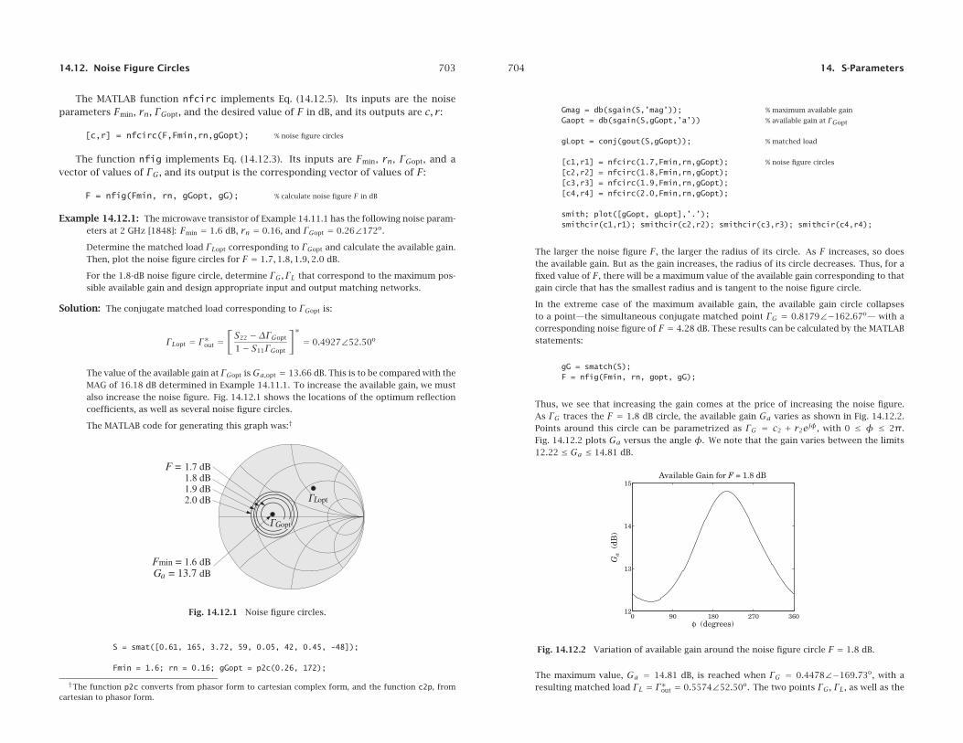
14.12. Noise Figure Circles 703
The MATLAB function nfcirc implements Eq. (14.12.5). Its inputs are the noiseparameters Fmin, rn, ΓGopt, and the desired value of F in dB, and its outputs are c, r:
[c,r] = nfcirc(F,Fmin,rn,gGopt); % noise figure circles
The function nfig implements Eq. (14.12.3). Its inputs are Fmin, rn, ΓGopt, and avector of values of ΓG, and its output is the corresponding vector of values of F:
F = nfig(Fmin, rn, gGopt, gG); % calculate noise figure F in dB
Example 14.12.1: The microwave transistor of Example 14.11.1 has the following noise param-eters at 2 GHz [1848]: Fmin = 1.6 dB, rn = 0.16, and ΓGopt = 0.26∠172o.
Determine the matched load ΓLopt corresponding to ΓGopt and calculate the available gain.Then, plot the noise figure circles for F = 1.7,1.8,1.9,2.0 dB.
For the 1.8-dB noise figure circle, determine ΓG, ΓL that correspond to the maximum pos-sible available gain and design appropriate input and output matching networks.
Solution: The conjugate matched load corresponding to ΓGopt is:
ΓLopt = Γ∗out =[S22 −ΔΓGopt
1− S11ΓGopt
]∗= 0.4927∠52.50o
The value of the available gain at ΓGopt isGa,opt = 13.66 dB. This is to be compared with theMAG of 16.18 dB determined in Example 14.11.1. To increase the available gain, we mustalso increase the noise figure. Fig. 14.12.1 shows the locations of the optimum reflectioncoefficients, as well as several noise figure circles.
The MATLAB code for generating this graph was:†
Fig. 14.12.1 Noise figure circles.
S = smat([0.61, 165, 3.72, 59, 0.05, 42, 0.45, -48]);
Fmin = 1.6; rn = 0.16; gGopt = p2c(0.26, 172);
†The function p2c converts from phasor form to cartesian complex form, and the function c2p, fromcartesian to phasor form.
704 14. S-Parameters
Gmag = db(sgain(S,’mag’)); % maximum available gain
Gaopt = db(sgain(S,gGopt,’a’)) % available gain at ΓGopt
gLopt = conj(gout(S,gGopt)); % matched load
[c1,r1] = nfcirc(1.7,Fmin,rn,gGopt); % noise figure circles
[c2,r2] = nfcirc(1.8,Fmin,rn,gGopt);[c3,r3] = nfcirc(1.9,Fmin,rn,gGopt);[c4,r4] = nfcirc(2.0,Fmin,rn,gGopt);
smith; plot([gGopt, gLopt],’.’);smithcir(c1,r1); smithcir(c2,r2); smithcir(c3,r3); smithcir(c4,r4);
The larger the noise figure F, the larger the radius of its circle. As F increases, so doesthe available gain. But as the gain increases, the radius of its circle decreases. Thus, for afixed value of F, there will be a maximum value of the available gain corresponding to thatgain circle that has the smallest radius and is tangent to the noise figure circle.
In the extreme case of the maximum available gain, the available gain circle collapsesto a point—the simultaneous conjugate matched point ΓG = 0.8179∠−162.67o— with acorresponding noise figure of F = 4.28 dB. These results can be calculated by the MATLABstatements:
gG = smatch(S);F = nfig(Fmin, rn, gopt, gG);
Thus, we see that increasing the gain comes at the price of increasing the noise figure.As ΓG traces the F = 1.8 dB circle, the available gain Ga varies as shown in Fig. 14.12.2.Points around this circle can be parametrized as ΓG = c2 + r2ejφ, with 0 ≤ φ ≤ 2π.Fig. 14.12.2 plots Ga versus the angle φ. We note that the gain varies between the limits12.22 ≤ Ga ≤ 14.81 dB.
0 90 180 270 36012
13
14
15
Ga
(dB
)φ (degrees)
Available Gain for F = 1.8 dB
Fig. 14.12.2 Variation of available gain around the noise figure circle F = 1.8 dB.
The maximum value, Ga = 14.81 dB, is reached when ΓG = 0.4478∠−169.73o, with aresulting matched load ΓL = Γ∗out = 0.5574∠52.50o. The two points ΓG, ΓL, as well as the

14.12. Noise Figure Circles 705
Fig. 14.12.3 Maximum available gain for given noise figure.
Ga = 14.81 dB gain circle, which is tangential to the 1.8-dB noise figure circle, are shownin Fig. 14.12.3.
The following MATLAB code performs these calculations and plots:
phi = linspace(0,2*pi,721); % angle in 1/2o increments
gG = c2 + r2*exp(j*phi); % ΓG around the c2, r2 circle
G = db(sgain(S,gG,’a’)); % available gain in dB
plot(phi*180/pi, G);
[Ga,i] = max(G); % maximum available gain
gammaG = gG(i); % ΓG for maximum gain
gammaL = conj(gout(S,gammaG)); % matched load ΓL
[ca,ra] = sgcirc(S,’a’,Ga); % available gain circle
smith; smithcir(c2,r2); smithcir(ca,ra);plot([gammaG,gammaL],’.’);
The maximum gain and the point of tangency with the noise figure circle are determined bydirect search, that is, evaluating the gain around the 1.8-dB noise figure circle and findingwhere it reaches a maximum.
The input and output stub matching networks can be designed with the help of the functionstub1. The normalized source and load impedances are:
zG = 1+ ΓG1− ΓG
= 0.3840− 0.0767j , zL = 1+ ΓL1− ΓL
= 1.0904+ 1.3993j
The stub matching networks have lengths:
stub1(z∗G,’po’)=[
0.3749 0.39770.1251 0.0738
], stub1(z∗L ,’po’)=
[0.3519 0.09910.1481 0.2250
]
The lower solutions have shorter total lengths d+ l. The implementation of the matchingnetworks with microstrip lines will be similar to that in Fig. 14.8.4. ��
706 14. S-Parameters
If the two-port is potentially unstable, one must be check that the resulting solutionsfor ΓG, ΓL both lie in their respective stability regions. Problems 14.6 and 14.7 illustratethe design of such potentially unstable low noise microwave amplifiers.
14.13 Problems
14.1 Using the relationships (14.4.3) and (14.4.6), derive the following identities:
(Z11 + ZG)(Z22 + ZL)−Z12Z21 =(Z22 + ZL)(Zin + ZG)= (Z11 + ZG)(Zout + ZL)
(14.13.1)
(1− S11ΓG)(1− S22ΓL)−S12S21ΓGΓL =(1− S22ΓL)(1− ΓinΓG)= (1− S11ΓG)(1− ΓoutΓL)
(14.13.2)
Using Eqs. (14.4.4) and (14.4.5), show that:
Z21
Z22 + ZL= S21
1− S22ΓL1− ΓL1− Γin
,Z21
Z11 + ZG= S21
1− S11ΓG1− ΓG1− Γout
(14.13.3)
2Z0
Zin + ZG= (1− Γin)(1− ΓG)
1− ΓinΓG,
2Z0
Zout + ZL= (1− Γout)(1− ΓL)
1− ΓoutΓL(14.13.4)
Finally, for the real part RL = Re(ZL), show that:
ZL = Z01+ ΓL1− ΓL
⇒ RL = Z01− |ΓL|2|1− ΓL|2 (14.13.5)
14.2 Computer Experiment. The Hewlett-Packard ATF-10136 GaAs FET transistor has the follow-ing S-parameters at 4 GHz and 8 GHz [1848]:
S11 = 0.54∠−120o , S21 = 3.60∠61o , S12 = 0.137∠31o , S22 = 0.22∠−49o
S11 = 0.60∠87o , S21 = 2.09∠−32o , S12 = 0.21∠−36o , S22 = 0.32∠−48o
Determine the stability parameters, stability circles, and stability regions at the two frequen-cies.
14.3 Derive the following relationships, where RG = Re(ZG):
Z0 + ZG2√RGZ0
= 1√1− |ΓG|2
|1− ΓG|1− ΓG
,Z0 − ZG2√RGZ0
= − ΓG√1− |ΓG|2
|1− ΓG|1− ΓG
14.4 Derive Eqs. (14.7.13) relating the generalized S-parameters of power waves to the conven-tional S-parameters.
14.5 Derive the expression Eq. (14.6.20) for the maximum available gain GMAG, and show that itis the maximum of all three gains, that is, transducer, available, and operating gains.
14.6 Computer Experiment. The microwave transistor of Example 14.11.2 has the following noiseparameters at a frequency of 1 GHz [1848]: Fmin = 1.3 dB, rn = 0.16, and ΓGopt = 0.06∠49o.
Determine the matched load ΓLopt corresponding to ΓGopt and calculate the available gain.Then, plot the noise figure circles for F = 1.4,1.5,1.6 dB.
For the 1.5-dB noise figure circle, determine the values of ΓG, ΓL that correspond to themaximum possible available gain.
Design microstrip stub matching circuits for the computed values of ΓG, ΓL.

14.13. Problems 707
14.7 Computer Experiment. The Hewlett-Packard ATF-36163 pseudomorphic high electron mo-bility transistor (PHEMT) has the following S- and noise parameters at 6 GHz [1848]:
S11 = 0.75∠−131o , S21 = 3.95∠55o , S12 = 0.13∠−12o , S22 = 0.27∠−116o
Fmin = 0.66 dB, rn = 0.15, ΓGopt = 0.55∠88o
Plot the F = 0.7,0.8,0.9 dB noise figure circles. On the 0.7-dB circle, determine the sourcereflection coefficient ΓG that corresponds to maximum available gain, and then determinethe corresponding matched load coefficient ΓL.
Design microstrip stub matching circuits for the computed values of ΓG, ΓL.
14.8 Computer Experiment. In this experiment, you will carry out two low-noise microwave am-plifier designs, including the corresponding input and output matching networks. The firstdesign fixes the noise figure and finds the maximum gain that can be used. The seconddesign fixes the desired gain and finds the minimum noise figure that may be achieved.
The Hewlett-Packard Agilent ATF-34143 PHEMT transistor is suitable for low-noise ampli-fiers in cellular/PCS base stations, low-earth-orbit and multipoint microwave distributionsystems, and other low-noise applications.
At 2 GHz, its S-parameters and noise-figure data are as follows, for biasing conditions ofVDS = 4 V and IDS = 40 mA:
S11 = 0.700∠−150o , S12 = 0.081∠19o
S21 = 6.002∠73o , S22 = 0.210∠−150o
Fmin = 0.22 dB, rn = 0.09, ΓGopt = 0.66∠67o
a. At 2 GHz, the transistor is potentially unstable. Calculate the stability parametersK,μ,Δ,D1,D2. Calculate the MSG in dB.
Draw a basic Smith chart and place on it the source and load stability circles (displayonly a small portion of each circle outside the Smith chart.)
Then, determine the parts of the Smith chart that correspond to the source and loadstability regions.
b. For the given optimum reflection coefficient ΓGopt, calculate the corresponding loadreflection coefficient ΓLopt assuming a matched load.
Place the two points ΓGopt, ΓLopt on the above Smith chart and determine whether theylie in their respective stability regions.
c. Calculate the available gain Ga,opt in dB that corresponds to ΓGopt.
Add the corresponding available gain circle to the above Smith chart. (Note that thesource stability circle and the available gain circles intersect the Smith chart at thesame points.)
d. Add to your Smith chart the noise figure circles corresponding to the noise figurevalues of F = 0.25,0.30,0.35 dB.
For the case F = 0.35 dB, calculate and plot the available gain Ga in dB as ΓG tracesthe noise-figure circle. Determine the maximum value of Ga and the correspondingvalue of ΓG.
Place on your Smith chart the available gain circle corresponding to this maximum Ga.Place also the corresponding point ΓG, which should be the point of tangency betweenthe gain and noise figure circles.
708 14. S-Parameters
Calculate and place on the Smith chart the corresponding load reflection coefficientΓL = Γ∗out. Verify that the two points ΓG, ΓL lie in their respective stability regions.
In addition, for comparison purposes, place on your Smith chart the available gaincircles corresponding to the values Ga = 15 and 16 dB.
e. The points ΓG and ΓL determined in the previous question achieve the maximum gainfor the given noise figure of F = 0.35 dB.
Design input and output stub matching networks that match the amplifier to a 50-ohmgenerator and a 50-ohm load. Use “parallel/open” microstrip stubs having 50-ohmcharacteristic impedance and alumina substrate of relative permittivity of εr = 9.8.
Determine the stub lengths d, l in units ofλ, the wavelength inside the microstrip lines.Choose always the solution with the shortest total length d+ l.Determine the effective permittivity εeff of the stubs, the stub wavelength λ in cm, andthe width/height ratio, w/h. Then, determine the stub lengths d, l in cm.
Finally, make a schematic of your final design that shows both the input and outputmatching networks (as in Fig.10.8.3.)
f. The above design sets F = 0.35 dB and finds the maximum achievable gain. Carry outan alternative design as follows. Start with a desired available gain of Ga = 16 dB anddraw the corresponding available gain circle on your Smith chart.
As ΓG traces the portion of this circle that lies inside the Smith chart, compute thecorresponding noise figure F. (Points on the circle can be parametrized by ΓG = c +rejφ, but you must keep only those that have |ΓG| < 1.)
Find the minimum among these values of F in dB and calculate the correspondingvalue of ΓG. Calculate the corresponding matched ΓL.
Add to your Smith chart the corresponding noise figure circle and place on it the pointsΓG and ΓL.
g. Design the appropriate stub matching networks as in part 14.8.