bit banged lin slave node for pic16 &...
TRANSCRIPT
AN239Bit Banged LIN Slave Node for PIC16 & PIC18
INTRODUCTIONThe Local Interconnect Network (LIN), as described inthe LIN v1.2 specification, is a multi-layered system. Thelevels vary from the physical interface up to the highlevel application. This application note focuses on theimplementation of a low level driver, essentially an inter-face between the physical hardware connection and thehigher level application firmware. Specifically, this appli-cation note presents a generic ‘bit banged’ LIN slavedriver for both the PIC16 and PIC18 family of PICmicro®
microcontrollers.
There are many details to this firmware design; how-ever, this application note focuses mainly on how to setup and use the driver. Therefore, the LIN systemdesigner should be able to get an application runningon LIN quickly without spending significant time on thedetails of LIN.
Some information about the firmware design is pro-vided at the end of this document for the curiousdesigner who wants to learn a little more about LIN andthis driver implementation.
The reader should note information in this applicationnote is presented with the assumption that the readeris familiar with LIN specification v1.2, the most currentspecification available at the time this document waswritten. Therefore, not all details about LIN are dis-cussed. Refer to the References section for additionalinformation.
APPLICATIONSThe first question that must be asked is: “Will this driverwork for my application?” The next few sections canhelp those who would like to know the answer to thisquestion and quickly decide whether this is the appro-priate driver implementation for their application. Theimportant elements that have significant weight on thedecision include available process time, resourceusage, and bit rate performance.
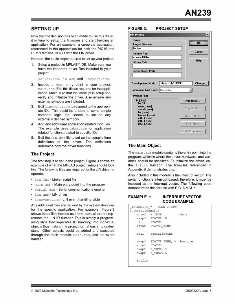
Process TimeAvailable process time is dictated predominately by bitrate, clock frequency, and code execution. Since codeexecution varies depending on the state within the LINdriver and there being many states, generating a singleequation for process time is unrealistic. A much simplersolution is to test the process time. Figure 1 shows theapproximate average available process time for a noderunning at 8 MHz.
FIGURE 1: AVAILABLE PROCESS TIME @ 8 MHz
When the LIN bus is IDLE, the driver uses significantlyless process time. Although dependent on the sameconditions stated above, the used process time isextremely low. At 8 MHz, the average availableprocess time is greater than 98%.
Resource UsageA few of the hardware resources are used to maintainrobust communications and precise timing. Timer0 isused for maintaining communications timing and busactivity time. In addition, the timer prescaler is adjustedunder various conditions to simplify the code andimprove performance in many states of the driver. Anexternal interrupt is used for START edge detection foreach received byte; either an interrupt-on-change pin,or the INT pin can be configured as the interruptsource.
Author: Ross FoslerMicrochip Technology Inc.
9.6K 19.2K
70%
80%
4.8K
50%
2002 Microchip Technology Inc. DS00239A-page 1

AN239
Bit RateBy selecting the appropriate clock frequency, the driveris designed to operate over the specified operatingrange of LIN: 1000 bps to 20000 bps. Note, however,that the clock must be selected such that at least 70instructions can be executed per every bit received.Refer to Figure 2 for recommended operating regions.SummaryThe driver is designed almost entirely in firmware. Onlythe hardware peripherals standard to PIC16 and PIC18MCUs are used. Thus, all communications and timingrequired by the LIN specification are controlled in firm-ware. This implies a certain percentage of softwareresources are consumed, most importantly, time. Toput this into perspective, at 19.2 Kbps using an 8 MHzoscillator source, an average of 50% of the processtime is used by the driver. Also, given the intolerance touncertainty, interrupts (high priority for PIC18) shouldbe restricted to the LIN communications driver whenthe instruction rate to bit rate ration (FOSC/B) is small(i.e., less than 200). For PIC18 devices, the low priorityinterrupt vector is available since low priority interruptsdo not interfere with high priority interrupts.
In summary, this basically means the PIC16 and PIC18bit banged drivers are well suited for applications thatdo not require excessive firmware processing and tighttiming. There are a number of peripherals available forthe PIC16 and PIC18 devices that can enhance theapplication without extensive firmware. Some of theseinclude A/D, PWM, USART, and comparators. Also, thePIC18 devices do have an advantage in that they havean extra interrupt vector and hardware stack manage-ment capability. Some applications could include motorcontrol, sensor feedback, on/off control, and indication.
FIGURE 2: RECOMMENDED OPERATING REGIONS
Clo
ck F
requ
ency
4 MHz
6 MHz
14k1.2kBit Rate
HS Mode Operation(1)
XT, and INTRC(1)
No Operation
20k2 MHz
7.2k
Note 1: Check specific device for available Oscillator modes.
DS00239A-page 2 2002 Microchip Technology Inc.
AN239
SETTING UP Now that the decision has been made to use this driver,it is time to setup the firmware and start building anapplication. For an example, a complete application,referenced in the appendixes for both the PIC16 andPIC18 families, is built with the LIN driver.
Here are the basic steps required to set up your project:
1. Setup a project in MPLAB® IDE. Make sure youhave the important driver files included in yourproject:
serial.asm, lin.asm, and linevent.asm.
2. Include a main entry point in your project:main.asm. Edit this file as required for the appli-cation. Make sure that the interrupt is setup cor-rectly and initialize the driver. Also ensure anyexternal symbols are included.
3. Edit linevent.asm to respond to the appropri-ate IDs. This could be a table or some simplecompare logic. Be certain to include anyexternally defined symbols.
4. Add any additional application related modules.The example uses idxx.asm for applicationrelated functions related to specific IDs.
5. Edit the lin.def file to set up the compile timedefinitions of the driver. The definitionsdetermine how the driver functions.
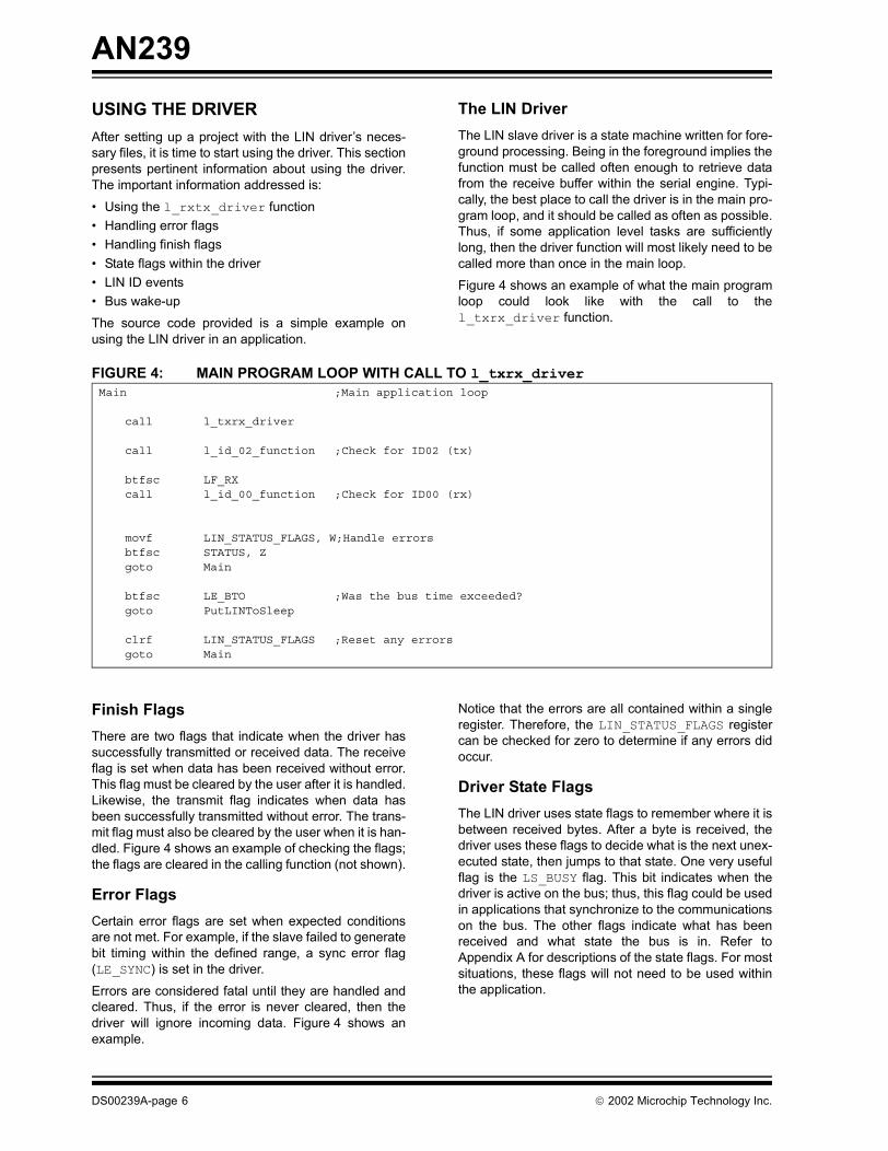
The ProjectThe first step is to setup the project. Figure 3 shows anexample of what the MPLAB project setup should looklike. The following files are required for the LIN driver tooperate:
• lin.lkr - Linker script file• main.asm - Main entry point into the program• serial.asm - Serial communications engine• lin.asm - LIN driver• linevent.asm - LIN event handling table
Any additional files are defined by the system designerfor the specific application. For example, Figure 3shows these files labeled as idxx.asm, where xx rep-resents the LIN ID number. This is simply a program-ming style that separates ID handling into individualobjects thus making the project format easier to under-stand. Other objects could be added and executedthrough the main module, main.asm, and the eventhandler.
FIGURE 3: PROJECT SETUP
The Main ObjectThe main.asm module contains the entry point into theprogram, which is where the driver, hardware, and vari-ables should be initialized. To initialize the driver, callthe l_init function. The firmware referenced inAppendix B demonstrates this.
Also included in this module is the interrupt vector. Theserial function is interrupt based; therefore, it must beincluded at the interrupt vector. The following codedemonstrates this for use with PIC16 MCUs.
EXAMPLE 1: INTERRUPT VECTOR CODE EXAMPLE
_INTERRUPT_V CODE 0x0004InterruptHandler
movwf W_TEMP ;Save swapf STATUS, Wclrf STATUSmovwf STATUS_TEMP
call SerialEngine
swapf STATUS_TEMP, W ;Restoremovwf STATUSswapf W_TEMP, Fswapf W_TEMP, W
retfie
2002 Microchip Technology Inc. DS00239A-page 3

AN239
The above example could also be used for PIC18MCUs; however, PIC18 MCUs have the Fast RegisterStack and a different interrupt vector. If the fast registerstack is used, then time and space could be saved byeliminating the context save and restore.DefinitionsThere are numerous compile time definitions, all ofthem located in lin.def, that are used to setup thesystem. Table 1 lists and describes these definitions.Likewise, the definitions are also listed in Appendix A.Only five of these definitions are critical for getting asystem running. They are:
• MAX_BIT_TIME• NOM_BIT_TIME• MIN_BIT_TIME• USE_GP_CHANGE• RX_ADVANCE (or RX_DELAY)The first three definitions, the bit time definitions, setupthe baud rate and its boundary for communication. Thenext item depends on the application hardware design.The LIN designer needs to setup an external STARTedge detection source; the two options are the INT pinor an interrupt-on-change pin. The last, yet very impor-tant definition, is the receive advance or delay. Thereceive advance (or delay) is used to advance (ordelay) the time-base to align to the center of the next bitafter the START bit.
LIN EventsLIN event functions are where the ID is decoded todetermine what to do next, transmit, receive, and howmuch. The designer should edit or modify the eventfunction to handle specific LIN IDs (see Appendix B foran example). One possibility is to set up a jump table.Another option is to set up some simple compare logic.The example firmware uses simple compare logic.
ID ModulesThe application firmware must be developed some-where in the project, it can be in main or in separatemodules; however, from a functional perspective, itdoes not matter. The example firmware uses separateID modules for individual handling of IDs and theirassociated functions. The most important part is toremember to include all the external symbols that areused. The symbols used by the driver are in lin.inc;this should be included in every application module.
DS00239A-page 4 2002 Microchip Technology Inc.

AN239
TABLE 1: COMPILE TIME DEFINITIONSDefinition Name Value Description
BRK_THRESHOLD d'11' Sets the receive break threshold. For low tolerance oscillator sources, this value should be ‘11’, for high tolerance sources, this value should be ‘9’.
LIN_ACTVE_TIME_PS b'10001000' The value loaded into the option register when the slave is actively receiving or transmitting on the LIN bus. A prescale value of 1x is ideal for bit rates between 4800 bps and 14400 bps at 4 MHz.
LIN_IDLE_TIME_PS b'10010110' The value loaded into the option register when the LIN bus is IDLE. A prescale setting of 128x is the desired choice for the prescaler.
LIN_SYNC_TIME_PS b'10010010' The value loaded into the option register when the slave is capturing the sync byte. A prescale setting of 8x is the desired choice for the prescaler.
MAX_BIT_TIME d'118' The upper boundary bit time for synchronization, which should equal ((FOSC x 1.15) / 4) /(bit rate) – 2
MAX_HEADER_TIME d'39' The maximum allowable time for the header. This value equals ((34 + 1) x 1.4) – 10, and should not be changed unless debugging.
MAX_IDLE_TIME d'195' Defines the maximum bus IDLE time; the spec defines this to be 25000 bit times. The value equals 25000 / 128. The 128 comes from the LIN_IDLE_TIME_PS defini-tion.
MAX_TIME_OUT d'128' Specifies the maximum time-out between wake-up requests. The LIN specification defines this to be 128 bit times.
MIN_BIT_TIME d'87' The lower boundary bit time for synchronization, which should equal ((FOSC x 0.85) / 4) /(bit rate) – 2
NOM_BIT_TIME d'102' The nominal bit time for synchronization, which should equal (FOSC / 4) /(bit rate) – 2
RC_OSC N/A Enables synchronization. Do not use this definition if using a crystal or resonator.
RX_ADVANCE 0x10 This is the receive advance. Use this definition to adjust center sampling for high bit rates, 7400 bps or greater at 4 MHz. RX_ADVANCE must not be used in conjunction with RX_DELAY.
RX_DELAY 0xF0 The receive delay. Use this definition to adjust center sampling for low bit rates, less than 7400 bps at 4 MHz. For lower bit rates, the delay should be longer. Note, this value is complimented (i.e., 0xF0 is a delay of 16 cycles). RX_DELAY must not be used in conjunction with RX_ADVANCE.
IO_MASK_A b'10111111' Logical AND mask of the transmit pin.
IO_MASK_O b'01000000' Logical OR mask of the I/O pin.
RX_PIN PORTC,7 The receive pin.
RX_PIN_DIR TRISC,7 The receive pin direction control.
TX_PIN PORTC,6 The transmit pin.
TX_PIN_DIR TRISC,6 The transmit pin direction control.
TX_PORT PORTC The transmit pin port.
USE_GP_CHANGE N/A Use this definition to configure the external interrupt to be a GPIO interrupt on change. The alternative is to use the INT pin.
2002 Microchip Technology Inc. DS00239A-page 5
AN239
USING THE DRIVERAfter setting up a project with the LIN driver’s neces-sary files, it is time to start using the driver. This sectionpresents pertinent information about using the driver.The important information addressed is:
• Using the l_rxtx_driver function• Handling error flags• Handling finish flags• State flags within the driver• LIN ID events• Bus wake-up
The source code provided is a simple example onusing the LIN driver in an application.
The LIN DriverThe LIN slave driver is a state machine written for fore-ground processing. Being in the foreground implies thefunction must be called often enough to retrieve datafrom the receive buffer within the serial engine. Typi-cally, the best place to call the driver is in the main pro-gram loop, and it should be called as often as possible.Thus, if some application level tasks are sufficientlylong, then the driver function will most likely need to becalled more than once in the main loop.
Figure 4 shows an example of what the main programloop could look like with the call to thel_txrx_driver function.
FIGURE 4: MAIN PROGRAM LOOP WITH CALL TO l_txrx_driver
Finish FlagsThere are two flags that indicate when the driver hassuccessfully transmitted or received data. The receiveflag is set when data has been received without error.This flag must be cleared by the user after it is handled.Likewise, the transmit flag indicates when data hasbeen successfully transmitted without error. The trans-mit flag must also be cleared by the user when it is han-dled. Figure 4 shows an example of checking the flags;the flags are cleared in the calling function (not shown).
Error FlagsCertain error flags are set when expected conditionsare not met. For example, if the slave failed to generatebit timing within the defined range, a sync error flag(LE_SYNC) is set in the driver.
Errors are considered fatal until they are handled andcleared. Thus, if the error is never cleared, then thedriver will ignore incoming data. Figure 4 shows anexample.
Notice that the errors are all contained within a singleregister. Therefore, the LIN_STATUS_FLAGS registercan be checked for zero to determine if any errors didoccur.
Driver State FlagsThe LIN driver uses state flags to remember where it isbetween received bytes. After a byte is received, thedriver uses these flags to decide what is the next unex-ecuted state, then jumps to that state. One very usefulflag is the LS_BUSY flag. This bit indicates when thedriver is active on the bus; thus, this flag could be usedin applications that synchronize to the communicationson the bus. The other flags indicate what has beenreceived and what state the bus is in. Refer toAppendix A for descriptions of the state flags. For mostsituations, these flags will not need to be used withinthe application.
Main ;Main application loop
call l_txrx_driver
call l_id_02_function ;Check for ID02 (tx)
btfsc LF_RXcall l_id_00_function ;Check for ID00 (rx)
movf LIN_STATUS_FLAGS, W;Handle errorsbtfsc STATUS, Zgoto Main
btfsc LE_BTO ;Was the bus time exceeded?goto PutLINToSleep
clrf LIN_STATUS_FLAGS ;Reset any errorsgoto Main
DS00239A-page 6 2002 Microchip Technology Inc.

AN239
ID Events and FunctionsFor each ID, there is an event function. The event func-tion is required to tell the driver how to respond to thedata following the ID. For example, does the driverneed to prepare to receive or transmit data? Also, howmuch data is expected to be received or transmitted?For successful operation three variables must be initial-ized, a pointer to data memory, frame time, and thecount, as shown in Figure 5.
FIGURE 5: VARIABLE INITIALIZATION
The pointer to memory tells the driver where to storedata for receiving or where to retrieve data for sending.The frame time is the adjusted time, based on thenumber of bytes to expect. Typically, the frame timeregister will already have time left over from the header,so time should be added to the register. For two bytes,this would be an additional (30 + 1) * 1.4 bit times, or43; the value 30 is the total bits of data, START bits, andSTOP bits, plus the checksum bits. The counter simplytells the driver how much data to operate on. Note thatthe count must always be initialized to somethinggreater than zero for the driver to function properly.
Waking the BusA LIN bus wake-up function, l_tx_wakeup, is pro-vided for applications that need the ability to wake thebus up. Calling this function will broadcast the wake-uprequest character.
GENERAL INFORMATION
Additional InterruptsIt is possible to add extra interrupts; however, it is notrecommended. The driver uses an external interrupt tosynchronize timing to the START edge. If additionalinterrupts are added, then uncertainty is added to thereceived START edge. Uncertainty in receiving theSTART edge can severely degrade the maximum bitrate under certain conditions.
There is a finite amount of uncertainty that is accept-able for a given bit rate and clock frequency, defined asfollows:
Without going into too much detail here, the aboveequation basically derives the maximum number ofinstructions related to uncertainty in terms of the idealbit rate and frequency (discussed later in this docu-ment). The real question is what instructions can becounted in this uncertainty and the answer is, itdepends on the way the code is written for the applica-tion. It is also important to note that some uncertainty isalready assumed.
To be safe (i.e., not sacrifice reliability), avoid addingany extra code to the interrupt unless your instructionrate to bit rate ratio is greater than 200, or the numberof instructions added is extremely small.
With PIC18 devices, you have the option of using thelow priority interrupt vector for additional interrupts. Thehigh priority interrupt should be used for the LIN driver,since it has precedence. The low priority interrupt couldbe used for any other interrupt source not related toLIN.
Definitions Using PrescalarsThe prescaler definitions are set to achieve bit ratesbetween 4800 bps and 14400 bps, using a 4 MHzclock source. It is possible to adjust these to achievelower bit rates or higher clock speeds. For example,multiplying all the prescaler values by two would yieldmuch lower bit rates, if desired.
The LIN Event HandlerEvent handling should be as short as possible. If theevent handler is long, unacceptable interbyte spacemay be seen between receiving the ID byte and trans-mitting data from the slave to the master. Therefore,choose the best method for decoding in your applica-tion. If you are only responding to a couple of IDs, thensimple XOR logical compares will suffice. If any moreIDs are responded to, then use a jump table. A com-plete jump table uses a significant amount of programmemory; however, it is very quick to decode IDs.
l_id_00 GLOBAL l_id_00
movlw ID00_BUFF ;Set the pointer movwf LIN_POINTER
movlw 0x20 ;Adjust the frame time addwf FRAME_TIME, F movlw 0x02 ;Set up the data count movwf LIN_COUNT retlw 0x00 ;Read
1BI----- TE1 low( ) TE2 high( ) 2TES+ +( )– Tw
4NINSFOSC---------------= =
2002 Microchip Technology Inc. DS00239A-page 7

AN239
Calling the DriverThe driver is not a true background task, only the serialcommunication is. Thus, the driver function must becalled frequently. There are two potential problems ifthe driver function is not called frequently enough. Thereceive buffer could be overrun, thus, the entire packetwould be corrupted. Another problem is unacceptableinterbyte space during slave to master transmissions.To be safe, ensure the driver function is called at leastfour times for every byte. The driver function willexecute very quickly if there is no action required.With the access to the hardware stack on the PIC18devices, it is possible to make the driver look like it isoperating in the background. Essentially, the addressof the driver function could be pushed onto the stackupon interrupt. When the serial communications fin-ishes, the address of the driver is pulled off the stack forexecution. when driver tasks are finished, controlreturns to the application. This method is a possibility;however, it is not shown.
Advance or DelayAfter detecting a START edge for a serial byte, there isa finite duration required to set up for the reception ofthe byte. Depending on the bit rate and frequency, theduration could put the sample point before or after thecenter of the next received bit. Thus, the advance anddelay options are available. The delay is used to holdsampling when the setup duration is shorter than halfthe bit time. The advance is used to advance the bittime for the next bit when the setup duration is longerthan half the bit time. The setup duration also includesthe time required to enter the interrupt, thus, the dura-tion depends significantly on how the interrupt is setup.PIC18 MCUs will have a slightly shorter setup time thanPIC16 MCUs, since time can be saved by using the fastregister stack.
IMPLEMENTATIONThere are five functions found in the associated exam-ple firmware that control the operation of the LINinterface:
• LIN Transmit/Receive Driver• LIN Serial Engine• LIN Timekeeper• LIN Hardware Initialization• LIN Wake-up
The Serial EngineThe serial engine is interrupt driven firmware. It han-dles all bit level communication and synchronization.The function requires an external interrupt source con-figurable to either an interrupt-on-change pin, or theINT pin. Also, Timer0 is used to control asynchronouscommunication.
SYNCHRONIZATION
Synchronization is performed by stretching the bit rateclock and using the external interrupt to count theedges of the sync byte. After the last falling edge of thesync byte, the time is captured and compared to themaximum and minimum bit time tolerances specified. Ifwithin the tolerance, the value is used as the newtime-base.
TRANSMITTING WITH READBACK
The software UART handles asynchronous communi-cations much like a hardware UART; it receives dataand generates errors under various conditions.Because the LIN physical layer has a feedback path fordata (see Figure 6), the UART also reads backtransmitted data.
FIGURE 6: SIMPLIFIED LIN TRANSCEIVER
The UART is designed to pre-sample before transmit-ting to capture feedback information. Transmit opera-tions take 11 bit times to accurately capture the last bitin the transmission.
SERIAL STATUS FLAGS
There are a few flags within the software UART to con-trol its operation and to feed status information to func-tions outside the UART. The serial status flags arelisted and defined in Appendix A.
VBAT
Open Drain
PIC16TX
RX
Buffer
LIN bus
DS00239A-page 8 2002 Microchip Technology Inc.

AN239
Transmit/Receive DriverThe l_rxtx_driver is a state machine. Bit flags areused to retain information about various states withinthe driver. In addition, status flags are maintained toindicate errors during transmit or receive operations.STATES AND STATE FLAGS
The LIN driver uses state flags to remember where it isbetween received bytes. After a byte is received, thedriver uses these flags to decide what is the next unex-ecuted state, then jumps to that state. Figure 7 andFigure 8 outline the program flow through the differentstates. The states and state flags are listed and definedin Appendix A.
TX/RX TABLE
A transmit/receive table is provided to determine howto handle data after the node has successfully receivedthe ID byte. The table returns information to thetransmit/receive driver about data size and direction.
STATUS FLAGS
Within various states, status flags may be set depend-ing on certain conditions. For example, if the slavereceives a corrupted checksum, then a checksum erroris indicated through a status flag. Unlike state flags,status flags are not reset automatically. Status flags areleft for the LIN system designer to act upon within thehigher levels of the firmware. The status flags are listedand defined in Appendix A.
LIN TimersThe LIN specification identifies maximum frame timesand bus IDLE times. For this reason, a timekeepingfunction is implemented. The timekeeping functionworks together with the transmit/receive driver and thetransmit and receive functions. Essentially, the driverand the transmit and receive functions update theappropriate time, and bus and frame time when called.If time-out conditions do occur, then status flags are setto indicate the condition.
Hardware InitializationAn initialization function, l_init, is provided to setupthe necessary hardware settings. Also, the state andstatus flags are all cleared. This function can also beused to reset the LIN driver.
Wake-upThe only time the slave can transmit to the bus withouta request is when the bus is sleeping. Basically, anyslave can transmit a wake-up signal. For this reason, awake-up function is defined, and it sends a wake-upsignal when called.
2002 Microchip Technology Inc. DS00239A-page 9

AN239
FIGURE 7: RECEIVE HEADER PROGRAM FLOWRequesting
No
Test Break, SetGot Break?
Got Sync? No
Yes
NoFlags
Yes
Finish
Measure andTest, Set Flags
Read Back Test,Yes Set Flags
Got ID?
Yes
TX or RX?
Wake-up?
Update Bus Timer
Build Option
Test ID, DetermineRX or TX,
Determine DataCount, Set FrameTimer, Set Flags
TX
No
A
B
RX
DS00239A-page 10 2002 Microchip Technology Inc.

AN239
FIGURE 8: TRANSMIT/RECEIVE MESSAGE PROGRAM FLOWTX or RX?
Yes
Test, Set FlagsRead Back?
Sent Whole No
Yes
No
Yes
Finish
Sent Checksum?
Yes
No
No
RX TX
Message?Test, Set Flags
Test, Set Flags
Test, Set Flags Got WholeMessage?
Read Checksum
Reset State Flags
B
2002 Microchip Technology Inc. DS00239A-page 11

AN239
FIGURE 9: TIMEKEEPING PROGRAM FLOWEVALUATING OPERATING REGIONIt is important to understand the relationship betweenbit rate and clock frequency when designing a slavenode in a LIN network. Therefore, this section focuseson developing this understanding based on the LINspecification. It is assumed that the physical limitsdefined in the LIN specification are reasonable andaccurate. This section merely uses the defined physicallimits and does not present any analysis of the limitsdefined for physical interface to the LIN bus. Essen-tially, the focus of this section is to analyze the firmwareand its performance based on the defined conditions inthe LIN specification.
General InformationSome general information used throughout theanalysis is provided here.
DATA RATE VS. SAMPLING RATE
There are essentially two rates to compare: the incom-ing data rate and the sampling rate. The slave nodeonly has control of the sampling rate; therefore, for thisdiscussion, the logical choice for a reference is theincoming data rate, BI. The equations that followassume BI is the ideal data rate of the system.
SAMPLING
The ideal sampling point is assumed to be the center ofthe incoming bit, as shown in Figure 10. The equationspresented in the following sections use this point as thereference.
FIGURE 10: SAMPLING
RELATING CLOCK FREQUENCY ERROR TO BIT ERROR
The LIN specification refers to clock frequency errorrather than bit error. Because of this, the LIN systemdesigner must design the system with like clock sources;however, this is rather impractical. It is more feasible tohave clock sources designed for the individual needs ofthe node. All of the equations in this section refer to biterror, rather than frequency error. The following equationrelates frequency error to bit rate error:
For very low clock frequency errors, the bit rate errorcan be approximated by:
Thus, a ±2% frequency error is nearly the same bit rateerror.
Finish
Update Bus TimeTest for Time-out
LIN bus Sleeping?
No
No YesActive TX/RX?Update FrameTime, Test for
Time-out
Start
Yes
11 EF+---------------- 1– EB=
E– F EB≈
DS00239A-page 12 2002 Microchip Technology Inc.

AN239
Acceptable Bit Rate ErrorThe LIN specification allows for a ±2% error for mas-ter/slave communications. This section evaluates thistolerance based on specified worst case conditions(slew rate, voltage, and threshold) and theimplementation.IDEAL SAMPLING WINDOW
It is relatively easy to see the maximum allowed errorin the ideal situation. Ideal is meant by infinite slew ratewith a purely symmetrical signal, like the signal shownin Figure 11.
FIGURE 11: IDEAL WINDOW
Basically, if the data sampling is greater or less thanhalf of one bit time, TE, over nine bits, the last bit in thetransmission will be interpreted incorrectly. Figure 12graphically depicts how data may be misinterpretedbecause of misaligned data and sampling rates.
FIGURE 12: DATA VS SAMPLING
The following two equations give the maximum andminimum bit rates based on shifting time by one-half ofone bit time or TE = ±1/(2BI).
SHORTENED WINDOW DUE TO SLEW RATE
Although the ideal sampling window may be a usefulapproximation at very low bit rates, slew rate andthreshold must be accounted for at higher rates. Theideal analysis serves as a base for more realisticanalysis.
The LIN specification defines a tolerable slew raterange and threshold. The worst case is the minimumslew rate at the maximum voltage, 1V/µs and 18V,according to the LIN specification. The threshold isabove 60% and below 40% for valid data. Figure 13shows the basic measurements.
FIGURE 13: ADJUSTED BIT TIME ERROR
Taking the difference of the ideal maximum time andthe slight adjustment due to specified operatingconditions yields the following error time adjustment:
Therefore, TE is slightly smaller than the ideal case,and the minimum and maximum equations in theprevious section yield a slightly narrower range for bitrate.
OFFSETS
An offset is a less than ideal sample point. For exam-ple, it is possible for a software UART to take a samplebefore or after the center point of an incoming bit, asshown in Figure 14. This is related to an offset from theSTART edge and ultimately shifts the bit rate error tofavor one side over the other. For example, if theSTART edge detection is delayed for 10 µs from thecenter of a 9.6 Kbit transmission, the absolute range forbit rate error is -4.1% and +6.9%.
FIGURE 14: OFFSET FROM CENTER
TE
VBAT
Ideal
Fast
Slow
1BI-----
TE9------– 1
Bmax------------=
1BI-----
TE9------+ 1
Bmin-----------=
TESTEI
VBAT
40%60%
TEI TES– 12BI-------- 0.5V 0.4V–( )
Vd( ) td( )⁄ min---------------------------------– TE= =
TEE
TEI
VBAT
40%60%
TO
2002 Microchip Technology Inc. DS00239A-page 13

AN239
The example firmware leaves the Timer0 interruptenabled at all times to maintain some basic time aboutthe LIN bus activity. A side effect of this is unpredictableoffset. For example, if a START edge occurs while pro-gram execution is in an interrupt, the interrupt routinemust finish before the START edge can be Acknowl-edged. Therefore, an undetermined offset from theSTART edge occurs.Although the exact offset cannot be determined wheninterrupts are enabled, it is possible to determine amaximum offset. Basically, the maximum offset isrelated to the longest time through the interrupt whenlooking for a START edge. Having the maximum offsetleads to the maximum bit rate.
The same equations apply as before; however, TE isdifferent for the maximum and minimum bit rate,because there is no time symmetry.
TE1 and TE2 are related:
where:
Ultimately, the LIN specification requires that the slaveaccept as much as a ±2% error between the incomingbit rate (BI) and the sampling bit rate. TE1 and TE2 havespecific limits for offsets before and after the centersampling point. They are:
With these times, the total window time shown inFigure 15, can be calculated to determine themaximum allowable offset or the maximum interruptduration:
FIGURE 15: ABSOLUTE OFFSET WINDOW
The 4/FOSC term is the instruction time. Multiplying theinstruction time by the number of executed instructionsin the interrupt routine results in the total time throughthe interrupt.
Substituting the time equations TE1(low), TE2(high), andTES, and solving BI yields the maximum bit rate:
Adjusting this down by 15% to allow for synchronizationtolerances leads to maximum allowable bit rate. Forexample, for a slave node operating at 4 MHz with amaximum instruction count of 40 through an interrupt,the maximum ideal bit rate would be about 14.2 kbps.Beyond 14.2 kbps, there is a significant probability thatincoming data will be misinterpreted.
Minimum Samples Per BitGiven a finite bit rate error range and finite control of thebit rate, leads to areas where the slave cannot operate.These are basically gaps where the error is outside thedefined bit rate error range for a particular number ofinstructions per bit. This section provides the mathe-matical basis for these gaps. The equations developedin this section are provided to help the LIN designerbuild a robust network.
FREQUENCY RANGE
The following equation determines the clock frequencyas a function of the number of instructions executed perbit, bit rate, and bit rate error.
1BI-----
TE19---------– 1
Bmax------------=
1BI-----
TE29---------+ 1
Bmin-----------=
1BI----- 2TES– TE1 TE2+=
TE2 TEI TES– TO–=
TE1 TEI TES– TO+=
TE2 high( )9 0.02–( )–0.98( ) BI( )--------------------------=
TE1 low( )9 0.02( )1.02( ) BI( )--------------------------=
1BI----- TE1 low( ) TE2 high( ) 2TES+ +( )– Tw
4NINSFOSC---------------= =
VBAT
40%60%
TE1(low) TE2(high)Tw
0.63994NF------- 1.8µs–---------------------------BI =0.6399
4NF------- 1.8µs–---------------------------
FOSC EB 1+( ) N( ) 4( ) B( )=
DS00239A-page 14 2002 Microchip Technology Inc.
AN239
OVERLAPPING OPERATIONFor a large number of instructions executed per bit, theslave will synchronize and communicate well with themaster. However, for a particular error range, ±2%, withhigher bit rates and lower clock frequencies, the slavemay never synchronize and communicate.
To approach this problem, the minimum frequency fora number of instructions (EL+1)(N)(4)(BI) must be com-pared to the maximum frequency for one less numberof instructions (EH+1)(N-1)(4)(BI). Where these areequal is the border between continuous anddiscontinuous operation for any given input frequency:
Solving this equation yields:
Therefore, the minimum number of instructions, Nlow,must be executed per bit to accept the defined error.For example, for a ±2% error, the lowest number ofinstructions accepted before certain clock frequency/bitrate combinations become a problem is 26. Note thatthe value of 26 is much lower than the number ofinstructions through the interrupt.
POSSIBLE ALTERNATE IMPLEMENTATIONThe bit banged firmware code referenced in this appli-cation note utilizes the Timer0 module and an externalinterrupt. It is also possible to use the CCP and Timer1module to perform the same function. The results arenearly the same as the implementation presented here.
MEMORY USAGEThe firmware code size depends on the build condi-tions. As it is currently built with the example applica-tion, the firmware occupies 412 words of programmemory and 46 bytes of data memory.
REFERENCESLIN Specification Package Revision 1.2, http://www.lin-subbus.org/
MPASM™ User’s Guide with MPLINK™ and MPLIB™,Microchip Technology Incorporated, 1999
EL 1+( ) N( ) 4( ) BI( ) EH 1+( ) N 1–( ) 4( ) BI( )=
NlowEH 1+( )
EH 1+( ) EL 1+( )–------------------------------------------------=
2002 Microchip Technology Inc. DS00239A-page 15

AN239
APPENDIX A: SYMBOLS
TABLE A-1: FUNCTIONS
TABLE A-2: REGISTERS
Function Name Purposel_init Call this function to initialize or reset the hardware associated to the LIN interface.l_tx_wakeup Wake-up function. Call this function to wake-up the bus if asleep.l_txrx_driver The core transmit and receive function, which manages transmit and receive operations to the bus.
State flags are set and cleared within this function. Status flags are also set based on certain conditions (i.e., errors).
l_txrx_table This function is called by the transmit/receive daemon after the identifier byte has been received. Message length and direction is returned to the driver. Within the table, pointers could be set up for different identifiers.
SerialEngine This is the interrupt driven software UART.UpdateTimer Used to update the bus and frame timers.
Variable Name PurposeBUS_TIME Bus timer.FRAME_TIME 8-bit frame timer register.HEADER_TIME Same as FRAME_TIME.LIN_CHKSUM Used by the driver to calculate checksum for transmit and receive.LIN_COUNT Used by the driver to maintain a message data count.LIN_FINISH_FLAGS Contains flags indicating completion of transmit and receive data.LIN_ID Holding register for the received identifier byte. This register is used in the l_txrx_table function to
determine how the node should react.LIN_POINTER Pointer to a storage area used by the driver. Data is either loaded into or read from memory depending
on the identifier.LIN_READBACK Holding register for transmitted data to be compared with received data for bit error detection.LIN_STATE_FLAGS Flags to indicate what state the LIN bus is in.LIN_STATE_FLAGS2 Additional flags to indicate what state the LIN bus is in.LIN_STATUS_FLAGS Contains status information about the LIN bus.RXDATA The Least Significant Byte of the receive shift register. The data is also pulled from this register after a
complete receive.RXSR_2 The Most Significant Byte of the receive shift register.RXTX_COUNT Bit counter register for the software UART.SERIAL_FLAGS This register holds the flags to control the software UART.TIME_BASE This register holds the time per bit based on the number of instructions.TXSR The Most Significant Byte of the transmit shift register.TXSR_2 The Least Significant Byte of the transmit shift register.
DS00239A-page 16 2002 Microchip Technology Inc.

AN239
TABLE A-3: FLAGSFlag Name Register MeaningLE_BIT LIN_STATUS_FLAGS Indicates a bit error.LE_BRK LIN_STATUS_FLAGS Indicates a failure to receive a valid break.LE_BTO LIN_STATUS_FLAGS Indicates a bus activity time-out error.LE_CHKSM LIN_STATUS_FLAGS Indicates a checksum error during a receive.LE_FTO LIN_STATUS_FLAGS Indicates a frame time-out error.LE_GEN LIN_STATUS_FLAGS Indicates a general error, typically a framing error.LE_PAR LIN_STATUS_FLAGS Indicates a parity error.LE_SYNC LIN_STATUS_FLAGS Indicates a synchronization tolerance error.LF_RX LIN_FINISH_FLAGS Indicates data has been received.LF_TX LIN_FINISH_FLAGS Indicates data has been sent.LS_BRK LIN_STATE_FLAGS Indicates a break has been received.LS_BUSY LIN_STATE_FLAGS Indicates the LIN bus is busy.LS_CHKSM LIN_STATE_FLAGS Indicates the checksum has been sent or received.LS_DATA LIN_STATE_FLAGS Indicates all data has been sent or received.LS_ID LIN_STATE_FLAGS Indicates the identifier has been received.LS_RBACK LIN_STATE_FLAGS Indicates a read back is pending.LS_SLPNG LIN_STATE_FLAGS Indicates the LIN bus is sleeping.LS_SYNC LIN_STATE_FLAGS Indicates a sync byte has been received.LS_TXRX LIN_STATE_FLAGS Indicates transmit or receive operation.LS_WAKE LIN_STATE_FLAGS Indicates a wake-up has been requested (this node only).S_BUSY SERIAL_FLAGS Indicates whether the serial engine is busy or not.S_FERR SERIAL_FLAGS Indicates an invalid STOP bit was received.S_RXIF SERIAL_FLAGS Indicates data has been received.S_SSRT SERIAL_FLAGS Indicates the serial engine is waiting for a start of sync.S_SYNC SERIAL_FLAGS Indicates the serial engine is syncing.S_SYNCERR SERIAL_FLAGS Indicates a failure to sync.S_TXRX SERIAL_FLAGS Indicates the UART is transmitting or receiving.
2002 Microchip Technology Inc. DS00239A-page 17

AN239
TABLE A-4: COMPILE TIME DEFINITIONS
Definition Name Value Description
BRK_THRESHOLD d'11' Sets the receive break threshold. For low tolerance oscillator sources, this value should be ‘11’, for high tolerance sources this value should be ‘9’.
LIN_ACTVE_TIME_PS b'10001000' The value loaded into the option register when the slave is actively receiving or transmitting on the LIN bus. A prescale value of 1x is ideal for bit rates between 4800 bps and 14400 bps at 4 MHz.
LIN_IDLE_TIME_PS b'10010110' The value loaded into the option register when the LIN bus is IDLE. A prescale setting of 128x is the desired choice for the prescaler.
LIN_SYNC_TIME_PS b'10010010' The value loaded into the option register when the slave is capturing the sync byte. A prescale setting of 8x is the desired choice for the prescaler.
MAX_BIT_TIME d'118' The upper boundary bit time for synchronization, which should equal ((FOSC x 1.15) / 4) /(bit rate) – 2
MAX_HEADER_TIME d'39' The maximum allowable time for the header. This value equals ((34 + 1) x 1.4) – 10, and should not be changed unless debugging.
MAX_IDLE_TIME d'195' Defines the maximum bus IDLE time; the spec defines this to be 25000 bit times. The value equals 25000 / 128. The 128 comes from the LIN_IDLE_TIME_PS definition.
MAX_TIME_OUT d'128' Specifies the maximum time out between wake-up requests. The LIN specification defines this to be 128 bit times.
MIN_BIT_TIME d'87' The lower boundary bit time for synchronization, which should equal ((FOSC x 0.85) / 4) /(bit rate) – 2
NOM_BIT_TIME d'102' The nominal bit time for synchronization, which should equal (FOSC / 4) /(bit rate) – 2
RC_OSC N/A Enables synchronization. Do not use this definition if using a crystal or resonator.
RX_ADVANCE 0x10 This is the receive advance. Use this definition to adjust center sampling for high bit rates, 7400 bps or greater at 4 MHz. RX_ADVANCE must not be used in conjunction with RX_DELAY.
RX_DELAY 0xF0 The receive delay. Use this definition to adjust center sampling for low bit rates, less than 7400 bps at 4 MHz. For lower bit rates, the delay should be longer. Note, this value is complimented (i.e., 0xF0 is a delay of 16 cycles). RX_DELAY must not be used in conjunction with RX_ADVANCE.
IO_MASK_A b'10111111' Logical AND mask of the transmit pin.
IO_MASK_O b'01000000' Logical OR mask of the I/O pin.
RX_PIN PORTC,7 The receive pin.
RX_PIN_DIR TRISC,7 The receive pin direction control.
TX_PIN PORTC,6 The transmit pin.
TX_PIN_DIR TRISC,6 The transmit pin direction control.
TX_PORT PORTC The transmit pin port.
USE_GP_CHANGE N/A Use this definition to configure the external interrupt to be a GPIO interrupt-on-change. The alternative is to use the INT pin.
DS00239A-page 18 2002 Microchip Technology Inc.

AN239
APPENDIX B: SOURCE CODEDue to size considerations, the complete source codefor this application note is not included in the text. Acomplete version of the source code, with all requiredsupport files, is available for download as a Zip archivefrom the Microchip web site, at:
www.microchip.com
2002 Microchip Technology Inc. DS00239A-page 19

AN239
NOTES:DS00239A-page 20 2002 Microchip Technology Inc.
Note the following details of the code protection feature on Microchip devices:• Microchip products meet the specification contained in their particular Microchip Data Sheet.
• Microchip believes that its family of products is one of the most secure families of its kind on the market today, when used in the intended manner and under normal conditions.
• There are dishonest and possibly illegal methods used to breach the code protection feature. All of these methods, to our knowl-edge, require using the Microchip products in a manner outside the operating specifications contained in Microchip's Data Sheets. Most likely, the person doing so is engaged in theft of intellectual property.
• Microchip is willing to work with the customer who is concerned about the integrity of their code.
• Neither Microchip nor any other semiconductor manufacturer can guarantee the security of their code. Code protection does not mean that we are guaranteeing the product as “unbreakable.”
Code protection is constantly evolving. We at Microchip are committed to continuously improving the code protection features of ourproducts.
Information contained in this publication regarding deviceapplications and the like is intended through suggestion onlyand may be superseded by updates. It is your responsibility toensure that your application meets with your specifications.No representation or warranty is given and no liability isassumed by Microchip Technology Incorporated with respectto the accuracy or use of such information, or infringement ofpatents or other intellectual property rights arising from suchuse or otherwise. Use of Microchip’s products as critical com-ponents in life support systems is not authorized except withexpress written approval by Microchip. No licenses are con-veyed, implicitly or otherwise, under any intellectual propertyrights.
2002 Microchip Technology Inc.
Trademarks
The Microchip name and logo, the Microchip logo, KEELOQ,MPLAB, PIC, PICmicro, PICSTART and PRO MATE areregistered trademarks of Microchip Technology Incorporatedin the U.S.A. and other countries.
FilterLab, microID, MXDEV, MXLAB, PICMASTER, SEEVALand The Embedded Control Solutions Company areregistered trademarks of Microchip Technology Incorporatedin the U.S.A.
dsPIC, dsPICDEM.net, ECONOMONITOR, FanSense,FlexROM, fuzzyLAB, In-Circuit Serial Programming, ICSP,ICEPIC, microPort, Migratable Memory, MPASM, MPLIB,MPLINK, MPSIM, PICC, PICDEM, PICDEM.net, rfPIC, SelectMode and Total Endurance are trademarks of MicrochipTechnology Incorporated in the U.S.A. and other countries.
Serialized Quick Turn Programming (SQTP) is a service markof Microchip Technology Incorporated in the U.S.A.
All other trademarks mentioned herein are property of theirrespective companies.
© 2002, Microchip Technology Incorporated, Printed in theU.S.A., All Rights Reserved.
Printed on recycled paper.
DS00239A - page 21
Microchip received QS-9000 quality system certification for its worldwide headquarters, design and wafer fabrication facilities in Chandler and Tempe, Arizona in July 1999 and Mountain View, California in March 2002. The Company’s quality system processes and procedures are QS-9000 compliant for its PICmicro® 8-bit MCUs, KEELOQ® code hopping devices, Serial EEPROMs, microperipherals, non-volatile memory and analog products. In addition, Microchip’s quality system for the design and manufacture of development systems is ISO 9001 certified.
DS00239A-page 22 2002 Microchip Technology Inc.
AMERICASCorporate Office2355 West Chandler Blvd.Chandler, AZ 85224-6199Tel: 480-792-7200 Fax: 480-792-7277Technical Support: 480-792-7627Web Address: http://www.microchip.com
Rocky Mountain2355 West Chandler Blvd.Chandler, AZ 85224-6199Tel: 480-792-7966 Fax: 480-792-4338
Atlanta500 Sugar Mill Road, Suite 200BAtlanta, GA 30350Tel: 770-640-0034 Fax: 770-640-0307
Boston2 Lan Drive, Suite 120Westford, MA 01886Tel: 978-692-3848 Fax: 978-692-3821
Chicago333 Pierce Road, Suite 180Itasca, IL 60143Tel: 630-285-0071 Fax: 630-285-0075
Dallas4570 Westgrove Drive, Suite 160Addison, TX 75001Tel: 972-818-7423 Fax: 972-818-2924
DetroitTri-Atria Office Building 32255 Northwestern Highway, Suite 190Farmington Hills, MI 48334Tel: 248-538-2250 Fax: 248-538-2260
Kokomo2767 S. Albright Road Kokomo, Indiana 46902Tel: 765-864-8360 Fax: 765-864-8387
Los Angeles18201 Von Karman, Suite 1090Irvine, CA 92612Tel: 949-263-1888 Fax: 949-263-1338
San JoseMicrochip Technology Inc.2107 North First Street, Suite 590San Jose, CA 95131Tel: 408-436-7950 Fax: 408-436-7955
Toronto6285 Northam Drive, Suite 108Mississauga, Ontario L4V 1X5, CanadaTel: 905-673-0699 Fax: 905-673-6509
ASIA/PACIFICAustraliaMicrochip Technology Australia Pty LtdSuite 22, 41 Rawson StreetEpping 2121, NSWAustraliaTel: 61-2-9868-6733 Fax: 61-2-9868-6755China - BeijingMicrochip Technology Consulting (Shanghai)Co., Ltd., Beijing Liaison OfficeUnit 915Bei Hai Wan Tai Bldg.No. 6 Chaoyangmen Beidajie Beijing, 100027, No. ChinaTel: 86-10-85282100 Fax: 86-10-85282104China - ChengduMicrochip Technology Consulting (Shanghai)Co., Ltd., Chengdu Liaison OfficeRm. 2401, 24th Floor, Ming Xing Financial TowerNo. 88 TIDU StreetChengdu 610016, ChinaTel: 86-28-86766200 Fax: 86-28-86766599China - FuzhouMicrochip Technology Consulting (Shanghai)Co., Ltd., Fuzhou Liaison OfficeUnit 28F, World Trade PlazaNo. 71 Wusi RoadFuzhou 350001, ChinaTel: 86-591-7503506 Fax: 86-591-7503521China - ShanghaiMicrochip Technology Consulting (Shanghai)Co., Ltd.Room 701, Bldg. BFar East International PlazaNo. 317 Xian Xia RoadShanghai, 200051Tel: 86-21-6275-5700 Fax: 86-21-6275-5060China - ShenzhenMicrochip Technology Consulting (Shanghai)Co., Ltd., Shenzhen Liaison OfficeRm. 1315, 13/F, Shenzhen Kerry Centre,Renminnan LuShenzhen 518001, ChinaTel: 86-755-82350361 Fax: 86-755-82366086China - Hong Kong SARMicrochip Technology Hongkong Ltd.Unit 901-6, Tower 2, Metroplaza223 Hing Fong RoadKwai Fong, N.T., Hong KongTel: 852-2401-1200 Fax: 852-2401-3431IndiaMicrochip Technology Inc.India Liaison OfficeDivyasree Chambers1 Floor, Wing A (A3/A4)No. 11, O’Shaugnessey RoadBangalore, 560 025, IndiaTel: 91-80-2290061 Fax: 91-80-2290062
JapanMicrochip Technology Japan K.K.Benex S-1 6F3-18-20, ShinyokohamaKohoku-Ku, Yokohama-shiKanagawa, 222-0033, JapanTel: 81-45-471- 6166 Fax: 81-45-471-6122KoreaMicrochip Technology Korea168-1, Youngbo Bldg. 3 FloorSamsung-Dong, Kangnam-KuSeoul, Korea 135-882Tel: 82-2-554-7200 Fax: 82-2-558-5934SingaporeMicrochip Technology Singapore Pte Ltd.200 Middle Road#07-02 Prime CentreSingapore, 188980Tel: 65-6334-8870 Fax: 65-6334-8850TaiwanMicrochip Technology (Barbados) Inc., Taiwan Branch11F-3, No. 207Tung Hua North RoadTaipei, 105, TaiwanTel: 886-2-2717-7175 Fax: 886-2-2545-0139
EUROPEAustriaMicrochip Technology Austria GmbHDurisolstrasse 2A-4600 WelsAustriaTel: 43-7242-2244-399Fax: 43-7242-2244-393DenmarkMicrochip Technology Nordic ApSRegus Business CentreLautrup hoj 1-3Ballerup DK-2750 DenmarkTel: 45 4420 9895 Fax: 45 4420 9910FranceMicrochip Technology SARLParc d’Activite du Moulin de Massy43 Rue du Saule TrapuBatiment A - ler Etage91300 Massy, FranceTel: 33-1-69-53-63-20 Fax: 33-1-69-30-90-79GermanyMicrochip Technology GmbHSteinheilstrasse 10D-85737 Ismaning, GermanyTel: 49-89-627-144 0 Fax: 49-89-627-144-44ItalyMicrochip Technology SRLCentro Direzionale Colleoni Palazzo Taurus 1 V. Le Colleoni 120041 Agrate BrianzaMilan, Italy Tel: 39-039-65791-1 Fax: 39-039-6899883United KingdomMicrochip Ltd.505 Eskdale RoadWinnersh TriangleWokingham Berkshire, England RG41 5TUTel: 44 118 921 5869 Fax: 44-118 921-5820
10/18/02
WORLDWIDE SALES AND SERVICE