binary adder and subtractor binary addition circuits
TRANSCRIPT

University of Basrah – College of Engineering – Computer Engineering Department Digital Logic - 1st
year – 2nd
Semester
1 Prepared by: Dr. Mohammed A. Al-Ebadi
Binary Adder and Subtractor
Binary Addition Circuits
1. Half Adder
A logic circuit block used for adding two one bit numbers or simply two bits is called as
a half adder circuit. This circuit has two inputs which accept the two bits and two
outputs, with one producing sum output and other produce carry output.
In the above half adder, inputs are labeled as A and B. The sum output is labeled with
the S and the carry output or carry out is labeled with Co. Half adder is mainly used for
addition of augend and addend of first order binary numbers.
Half adder has limited number of applications, and practically not used in the
application especially multi-digit addition. In such applications carry of the previous
digit addition must be added along with two bits; hence it is three bits addition.

University of Basrah – College of Engineering – Computer Engineering Department Digital Logic - 1st
year – 2nd
Semester
2 Prepared by: Dr. Mohammed A. Al-Ebadi
2. Full Adder
A binary full adder is a multiple output combinational logic network that performs the
arithmetic sum of three input bits. As we have seen that the half adder cannot respond to
the three inputs and hence the full adder is used to add three digits at a time.
It consists of three inputs, in which two are input variables represent the two significant
bits to be added, labeled as A and B, whereas the third input terminal is the carry from
the previous lower significant position and labeled as Cin. The two outputs are a sum
and a carry outputs which are labeled as S and Cout respectively.
Full adder can be formed by combining two half adders and an OR gate as shown in
above where output and carry-in of the first adder becomes the input to the second half
adder that produce the total sum output. The total carry out is produced by ORing the
two half adder carry outs as shown in figure. The full adder block diagram and truth
table is shown below.

University of Basrah – College of Engineering – Computer Engineering Department Digital Logic - 1st
year – 2nd
Semester
3 Prepared by: Dr. Mohammed A. Al-Ebadi
3. Parallel Binary Adders
As we discussed that a single full adder performs the addition of two one bit numbers
and an input carry. For performing the addition of binary numbers with more than one
bit, more than one full adder is required depends on the number bits. Thus, a parallel
adder is used for adding all bits of the two numbers simultaneously.
By connecting a number of full adders in parallel, n-bit parallel adder is constructed.
From the below figure, it is to be noted that there is no carry at the least significant
position, hence we can use either a half adder or made the carry input of full adder to
zero at this position.

University of Basrah – College of Engineering – Computer Engineering Department Digital Logic - 1st
year – 2nd
Semester
4 Prepared by: Dr. Mohammed A. Al-Ebadi
The figure below shows a parallel 4 bit binary adder which has three full adders and one
half-adder. The two binary numbers to be added are A3A2A1A0 and B3B2B1B0 which
are applied to the corresponding inputs of full adders. This parallel adder produces their
sum as C4S3S2S1S0 where C4 is the final carry.
In the 4 bit adder, first block is a half-adder that has two inputs as A0B0 and produces
their sum S0 and a carry bit C1. Next block should be full adder as there are three inputs
applied to it. Hence this full adder produces their sum S1 and a carry C2. This will be
followed by other two full adders and thus the final sum is C4S3S2S1S0.
Most commonly Full adders designed in dual in-line package integrated circuits. A
typical 74LS283 is a 4 bit full adder. Arithmetic and Logic Unit of a unit computer
consist of these parallel adders to perform the addition of binary numbers.

University of Basrah – College of Engineering – Computer Engineering Department Digital Logic - 1st
year – 2nd
Semester
5 Prepared by: Dr. Mohammed A. Al-Ebadi
Binary Subtraction Circuits
1. Half Subtractor
A half subtractor is a multiple output combinational logic network that does the
subtraction of two bits of binary data. It has input variables and two output variables.
Two inputs are corresponding to two input bits and two output variables correspond to
the difference bit and borrow bit.
The binary subtraction is also performed by the Ex-OR gate with additional circuitry to
perform the borrow operation. Thus, a half subtractor is designed by an Ex-OR gate
including AND gate with A input complemented before fed to the gate.
The block model, truth table and logic diagram of a half subtractor shown in above
figure. This circuit is similar to the half adder with only difference in input A i.e.,
minuend which is complemented before applied at the AND gate to implement the
borrow output.

University of Basrah – College of Engineering – Computer Engineering Department Digital Logic - 1st
year – 2nd
Semester
6 Prepared by: Dr. Mohammed A. Al-Ebadi
In case of multi-digit subtraction, subtraction between the two digits must be performed
along with borrow of the previous digit subtraction, and hence a subtractor needs to
have three inputs. Therefore, a half subtractor has limited applications and strictly it is
not used in practice.
2. Full Subtractor
A combinational logic circuit performs a subtraction between the two binary bits by
considering borrow of the lower significant stage is called as the full subtractor. In this,
subtraction of the two digits is performed by taking into consideration whether a 1 has
already borrowed by the previous adjacent lower minuend bit or not.
It has three input terminals in which two terminals corresponds to the two bits to be
subtracted (minuend A and subtrahend B), and a borrow bit Bi corresponds to the
borrow operation. There are two outputs, one corresponds to the difference D output
and other borrow output BO as shown in figure along with truth table.
By deriving the Boolean expression for the full subtractor from above truth table, we get
the expression that tells that a full subtractor can be implemented with two half
subtractors and OR gate as shown in figure below.
University of Basrah – College of Engineering – Computer Engineering Department Digital Logic - 1st
year – 2nd
Semester
7 Prepared by: Dr. Mohammed A. Al-Ebadi
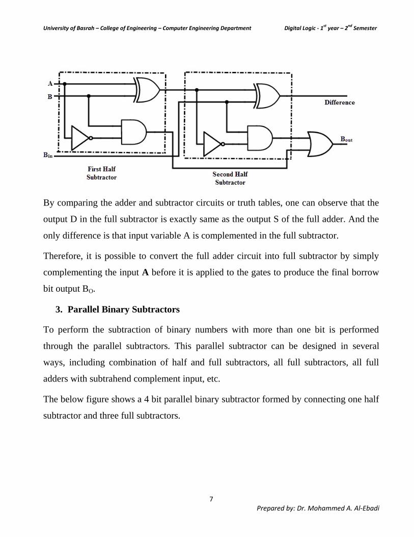
By comparing the adder and subtractor circuits or truth tables, one can observe that the
output D in the full subtractor is exactly same as the output S of the full adder. And the
only difference is that input variable A is complemented in the full subtractor.
Therefore, it is possible to convert the full adder circuit into full subtractor by simply
complementing the input A before it is applied to the gates to produce the final borrow
bit output BO.
3. Parallel Binary Subtractors
To perform the subtraction of binary numbers with more than one bit is performed
through the parallel subtractors. This parallel subtractor can be designed in several
ways, including combination of half and full subtractors, all full subtractors, all full
adders with subtrahend complement input, etc.
The below figure shows a 4 bit parallel binary subtractor formed by connecting one half
subtractor and three full subtractors.

University of Basrah – College of Engineering – Computer Engineering Department Digital Logic - 1st
year – 2nd
Semester
8 Prepared by: Dr. Mohammed A. Al-Ebadi
In this subtractor, 4 bit minuend A3A2A1A0 is subtracted by 4 bit subtrahend B3B2B1B0
and gives the difference output D3D2D1D0. The borrow output of each subtractor is
connected as the borrow input to the next preceding subtractor.
It is also possible to design a 4 bit parallel subtractor by 4 full adders as shown in the
below figure.
This circuit performs the subtraction operation by considering the principle that the
addition of minuend and the complement of the subtrahend is equivalent to the
subtraction process.
University of Basrah – College of Engineering – Computer Engineering Department Digital Logic - 1st
year – 2nd
Semester
9 Prepared by: Dr. Mohammed A. Al-Ebadi
We know that the subtraction of A by B is obtained by taking 2’s complement of B and
adding it to A. The 2’s complement of B is obtained by taking 1’s complement and
adding 1 to the least significant pair of bits.
Hence, in this circuit 1’s complement of B is obtained with the inverters (NOT gate) and
a 1 can be added to the sum through the input carry.
Parallel Adder / Subtractor
The operations of both addition and subtraction can be performed by a one common
binary adder. Such binary circuit can be designed by adding an Ex-OR gate with each
full adder as shown in below figure. The figure below shows the 4 bit parallel binary
adder/subtractor which has two 4 bit inputs as A3A2A1A0 and B3B2B1B0.
The mode input control line M is connected with carry input of the least significant bit
of the full adder. This control line decides the type of operation, whether addition or
subtraction.
When M= 1, the circuit is a subtractor and when M=0, the circuit becomes adder. The
Ex-OR gate consists of two inputs to which one is connected to the B and other to input

University of Basrah – College of Engineering – Computer Engineering Department Digital Logic - 1st
year – 2nd
Semester
10 Prepared by: Dr. Mohammed A. Al-Ebadi
M. When M = 0, B Ex-OR of 0 produce B. Then full adders add the B with A with carry
input zero and hence an addition operation is performed.
When M = 1, B Ex-OR of 0 produce B complement and also carry input is 1. Hence the
complemented B inputs are added to A and 1 is added through the input carry, nothing
but a 2’s complement operation. Therefore, the subtraction operation is performed.
University of Basrah – College of Engineering – Computer Engineering Department Digital Logic – 1st
year – 2nd
Semester
1 Prepared by: Dr. Mohammed Al-Ebadi
Latches and Flip-Flops
1. Introduction
Sequential switching circuits have the property that the output depends not only on
the present input but also on the past sequence of inputs. In effect, these circuits
must be able to “remember” something about the past history of the inputs in order
to produce the present output. Latches and flip-flops are commonly used memory
devices in sequential circuits. Basically, latches and flip-flops are memory devices
which can assume one of two stable output states and which have one or more
inputs that can cause the output state to change.
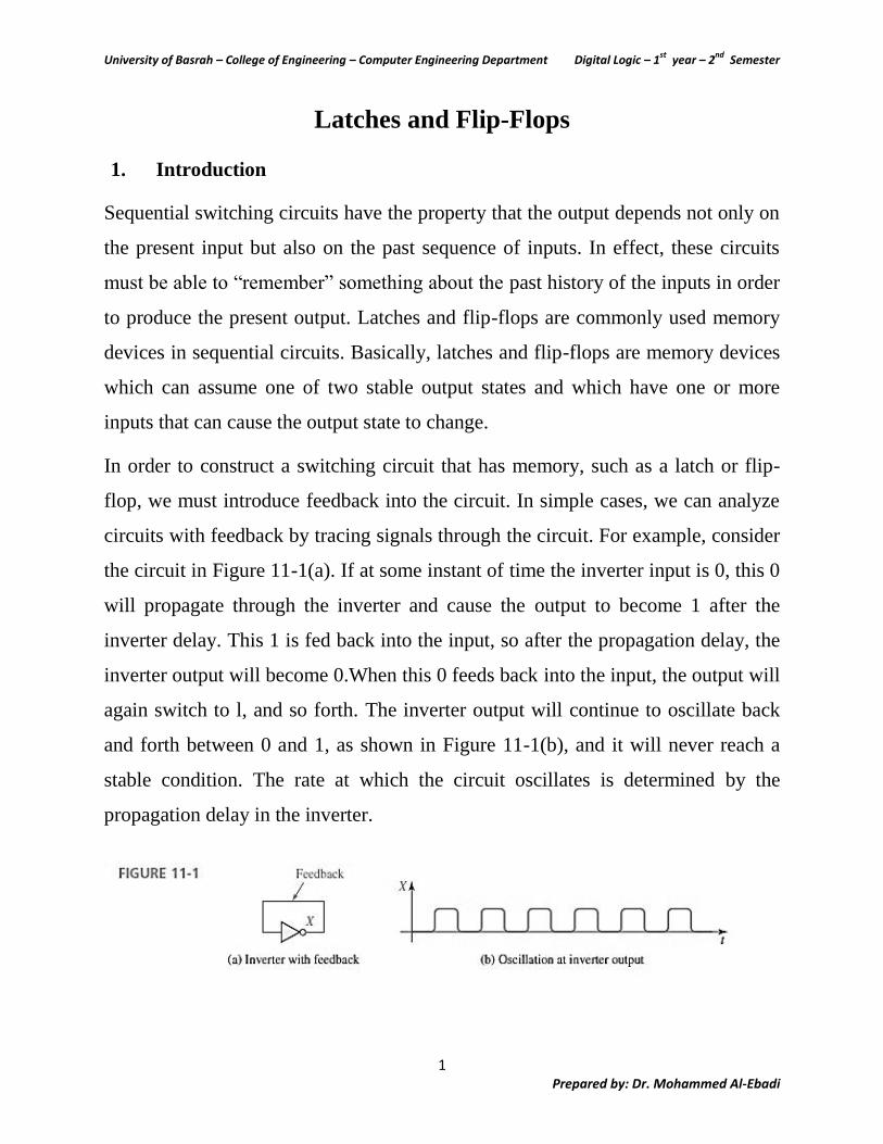
In order to construct a switching circuit that has memory, such as a latch or flip-
flop, we must introduce feedback into the circuit. In simple cases, we can analyze
circuits with feedback by tracing signals through the circuit. For example, consider
the circuit in Figure 11-1(a). If at some instant of time the inverter input is 0, this 0
will propagate through the inverter and cause the output to become 1 after the
inverter delay. This 1 is fed back into the input, so after the propagation delay, the
inverter output will become 0.When this 0 feeds back into the input, the output will
again switch to l, and so forth. The inverter output will continue to oscillate back
and forth between 0 and 1, as shown in Figure 11-1(b), and it will never reach a
stable condition. The rate at which the circuit oscillates is determined by the
propagation delay in the inverter.

University of Basrah – College of Engineering – Computer Engineering Department Digital Logic – 1st
year – 2nd
Semester
2 Prepared by: Dr. Mohammed Al-Ebadi
Next, consider a feedback loop which has two inverters in it, as shown in Figure
11-2(a). In this case, the circuit has two stable conditions, often referred to as
stable states. If the input to the first inverter is 0, its output will be 1.Then, the
input to the second inverter will be 1, and its output will be 0.This 0 will feed back
into the first inverter, but because this input is already 0, no changes will occur.
The circuit is then in a stable state. As shown in Figure 11-2(b), a second stable
state of the circuit occurs when the input to the first inverter is 1 and the input to
the second inverter is 0.
2. Set-Reset Latch
We can construct a simple latch by introducing feedback into a NOR-gate circuit,
as seen in Figure 11-3(a). As indicated, if the inputs are S = R = 0, the circuit can
assume a stable state with Q = 0 and P = 1. Note that this is a stable condition of
the circuit because P = 1 feeds into the second gate forcing the output to be Q = 0,
and Q = 0 feeds into the first gate allowing its output to be 1. Now if we change S
to 1, P will become 0. This is an unstable condition or state of the circuit because
both the inputs and output of the second gate are 0; therefore Q will change to 1,
leading to the stable state shown in Figure 11-3(b).

University of Basrah – College of Engineering – Computer Engineering Department Digital Logic – 1st
year – 2nd
Semester
3 Prepared by: Dr. Mohammed Al-Ebadi
If S is changed back to 0, the circuit will not change state because Q = 1 feeds back
into the first gate, causing P to remain 0, as shown in Figure 11-4(a). Note that the
inputs are again S = R = 0, but the outputs are different than those with which we
started. Thus, the circuit has two different stable states for a given set of inputs.
If we now change R to 1, Q will become 0 and P will then change back to 1, as
seen in Figure 11-4(b). If we then change R back to 0, the circuit remains in this
state and we are back where we started.
This circuit is said to have memory because its output depends not only on the
present inputs, but also on the past sequence of inputs. If we restrict the inputs so
that R = S = 1 is not allowed, the stable states of the outputs P and Q are always
complements, that is, P = Qʹ.
As shown in Figures 11-3(b) and 11-4(b), an input S = 1 sets the output to Q = 1,
and an input R = 1 resets the output to Q = 0.When used with the restriction that R
and S cannot be 1 simultaneously, the circuit is commonly referred to as a set-reset
(S-R) latch and given the symbol shown in Figure 11-5(b). Note that although Q
comes out of the NOR gate with the R input, the standard S-R latch symbol has Q
directly above the S input.

University of Basrah – College of Engineering – Computer Engineering Department Digital Logic – 1st
year – 2nd
Semester
4 Prepared by: Dr. Mohammed Al-Ebadi
The timming diagram below summerizes the operation of S-R latch.
Figure 11-8 shows the truth table and the derivation of Q+ for an S-R latch. From
the K-map, it’s clear that Q+= S +RʹQ where (S.R= 0). This equation is called the
next-state equation, or characteristic equation.

University of Basrah – College of Engineering – Computer Engineering Department Digital Logic – 1st
year – 2nd
Semester
5 Prepared by: Dr. Mohammed Al-Ebadi
An alternative form of the S-R latch uses NAND gates, as shown in Figure 11-10.
We will refer to this circuit as an ̅- ̅ latch, and the table describes its operation.
We have labeled the inputs to this latch ̅ and ̅ because S= 0 will set Q to 1 and
R= 0 will reset Q to 0. If ̅ and ̅ are 0 at the same time, both the Q and Qʹ outputs
are forced to 1.Therefore, for the proper operation of this latch, the condition ̅ = ̅
= 0 is not allowed.
3. Gated D Latch
A gated D latch (Figure 11-11) has two inputs, a data input (D) and a gate input
(G). The D latch can be constructed from an S-R latch and gates (Figure 11-
1(a)).When G = 0, S = R =0, so Q does not change. When G = 1 and D = 1, S = 1
and R = 0, so Q is set to 1.When G = 1 and D = 0, S = 0 and R = 1, so Q is reset to
0. In other words, when G = 1, the Q output follows the D input, and when G = 0,
the Q output holds the last value of D (no state change). This type of latch is also
referred to as a transparent latch because when G = 1, the Q output is the same as
the D input. From the truth table (Figure 11-12), the characteristic equation for
the latch is Q+ = GʹQ + GD

University of Basrah – College of Engineering – Computer Engineering Department Digital Logic – 1st
year – 2nd
Semester
6 Prepared by: Dr. Mohammed Al-Ebadi
4. Edge-Triggered D Flip-Flop
D flip-flop (Figure 11-13) has two inputs, D (data) and Ck (clock). The small
arrowhead on the flip-flop symbol identifies the clock input. Unlike the D latch,
the flip-flop output changes only in response to the clock, not to a change in D. If
the output can change in response to a 0 to 1 transition on the clock input, we say
that the flip-flop is triggered on the rising edge (or positive edge) of the clock. If
the output can change in response to a 1 to 0 transition on the clock input, we say
that the flip-flop is triggered on the falling edge (or negative edge) of the clock.
An inversion bubble on the clock input indicates a falling-edge trigger (Figure 11-
13(b)), and no bubble indicates a rising-edge trigger [Figure 11-13(a)].The term
active edge refers to the clock edge (rising or falling) that triggers the flip-flop
state change.

University of Basrah – College of Engineering – Computer Engineering Department Digital Logic – 1st
year – 2nd
Semester
7 Prepared by: Dr. Mohammed Al-Ebadi
The state of a D flip-flop after the active clock edge (Q+) is equal to the input (D)
before the active edge. For example, if D = 1 before the clock pulse, Q = 1 after the
active edge, regardless of the previous value of Q. Therefore, the characteristic
equation is Q+ = D. If D changes at most once following each clock pulse, the
output of the flip-flop is the same as the D input, except that the output changes are
delayed until after the active edge of the clock pulse, as illustrated in Figure 11-14.
A rising-edge-triggered D flip-flop can be constructed from two gated D latches
and an inverter, as shown in Figure 11-15(a).The timing diagram is shown in
Figure 11-15(b).
University of Basrah – College of Engineering – Computer Engineering Department Digital Logic – 1st
year – 2nd
Semester
8 Prepared by: Dr. Mohammed Al-Ebadi
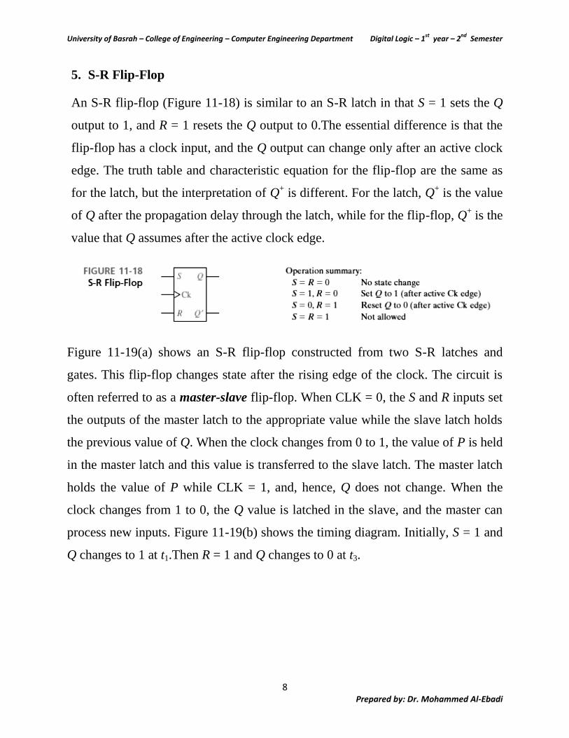
5. S-R Flip-Flop
An S-R flip-flop (Figure 11-18) is similar to an S-R latch in that S = 1 sets the Q
output to 1, and R = 1 resets the Q output to 0.The essential difference is that the
flip-flop has a clock input, and the Q output can change only after an active clock
edge. The truth table and characteristic equation for the flip-flop are the same as
for the latch, but the interpretation of Q+ is different. For the latch, Q
+ is the value
of Q after the propagation delay through the latch, while for the flip-flop, Q+ is the
value that Q assumes after the active clock edge.
Figure 11-19(a) shows an S-R flip-flop constructed from two S-R latches and
gates. This flip-flop changes state after the rising edge of the clock. The circuit is
often referred to as a master-slave flip-flop. When CLK = 0, the S and R inputs set
the outputs of the master latch to the appropriate value while the slave latch holds
the previous value of Q. When the clock changes from 0 to 1, the value of P is held
in the master latch and this value is transferred to the slave latch. The master latch
holds the value of P while CLK = 1, and, hence, Q does not change. When the
clock changes from 1 to 0, the Q value is latched in the slave, and the master can
process new inputs. Figure 11-19(b) shows the timing diagram. Initially, S = 1 and
Q changes to 1 at t1.Then R = 1 and Q changes to 0 at t3.

University of Basrah – College of Engineering – Computer Engineering Department Digital Logic – 1st
year – 2nd
Semester
9 Prepared by: Dr. Mohammed Al-Ebadi
6. J-K Flip-Flop
The J-K flip-flop (Figure 11-20) is an extended version of the S-R flip-flop.
The J-K flip-flop was named after Jack Kilby, the Texas Instruments engineer that
invented the integrated circuit in 1958. The J-K flip-flop has three inputs: J, K,
and the clock (CK).The J input corresponds to S, and K corresponds to R. That is,
if J = 1 and K = 0, the flip-flop output is set to Q = 1 after the active clock edge;
and if K = 1 and J = 0, the flip-flop output is reset to Q = 0 after the active edge.
Unlike the S-R flip-flop, a 1 input may be applied simultaneously to J and K, in
which case the flip-flop changes state after the active clock edge. When J = K = 1,
the active edge will cause Q to change from 0 to 1, or from 1 to 0.The next state
table and characteristic equation for the J-K flip-flop are given in Figure 11-20(b).
Figure 11-20(c) shows the timing for a J-K flip-flop.

University of Basrah – College of Engineering – Computer Engineering Department Digital Logic – 1st
year – 2nd
Semester
10 Prepared by: Dr. Mohammed Al-Ebadi
One way to realize the J-K flip-flop is with two S-R latches connected in a master-
slave arrangement, as shown in Figure 11-21. This is the same circuit as for the S-R
master-slave flip-flop, except S and R have been replaced with J and K, and the Q
and Qʹ outputs are feeding back into the input gates. Because S=J∙Qʹ∙Clkʹ and
R=K∙Q∙Clkʹ, only one of S and R inputs to the first latch can be 1 at any given time.
If Q = 0 and J = 1, then S = 1 and R = 0, regardless of the value of K. If Q = 1 and
K = 1, then S = 0 and R = 1, regardless of the value of J.

University of Basrah – College of Engineering – Computer Engineering Department Digital Logic – 1st
year – 2nd
Semester
11 Prepared by: Dr. Mohammed Al-Ebadi
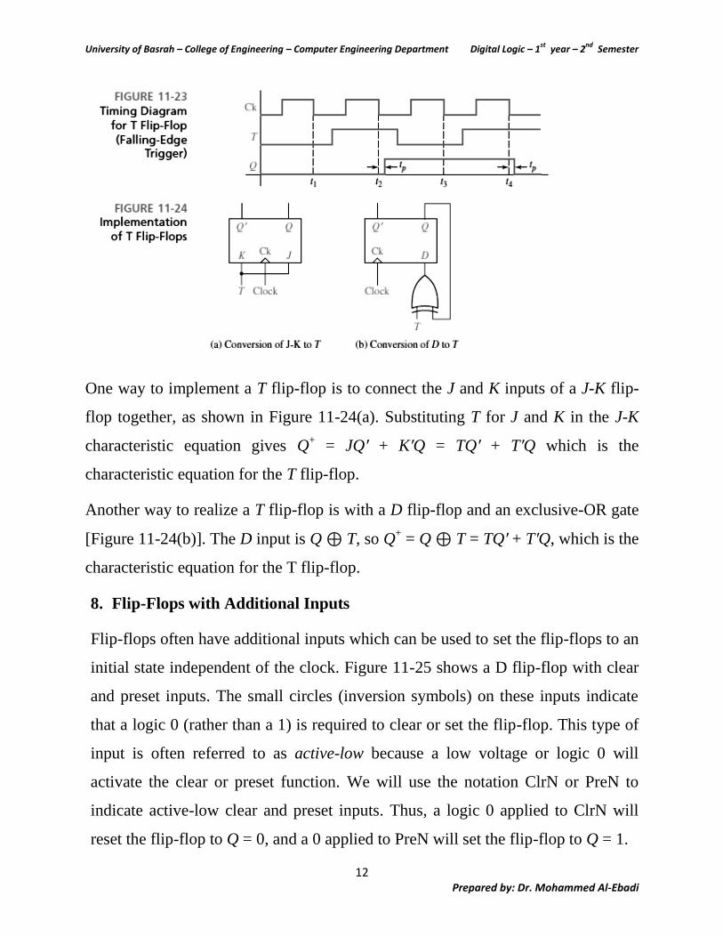
7. T Flip-Flop
The T flip-flop, also called the toggle flip-flop, is frequently used in building
counters. The T flip-flop in Figure 11-22(a) has a T input and a clock input. When
T = 1 the flip-flop changes state after the active edge of the clock. When T = 0, no
state change occurs. The next state table and characteristic equation for the T flip-
flop are given in Figure 11-22(b). The characteristic equation states that the next
state of the flip-flop (Q+) will be 1 if and only if the present state (Q) is 1 and T = 0
or the present state is 0 and T = 1. Figure 11-23 shows a timing diagram for the T
flip-flop. At times t2 and t4 the T input is 1 and the flip-flop state (Q) changes a
short time (tp) after the falling edge of the clock pulse. At times tl and t3 the T input
is 0, and the clock edge does not cause a change of state.
University of Basrah – College of Engineering – Computer Engineering Department Digital Logic – 1st
year – 2nd
Semester
12 Prepared by: Dr. Mohammed Al-Ebadi
One way to implement a T flip-flop is to connect the J and K inputs of a J-K flip-
flop together, as shown in Figure 11-24(a). Substituting T for J and K in the J-K
characteristic equation gives Q+ = JQʹ + KʹQ = TQʹ + TʹQ which is the
characteristic equation for the T flip-flop.
Another way to realize a T flip-flop is with a D flip-flop and an exclusive-OR gate
[Figure 11-24(b)]. The D input is Q ⊕ T, so Q+ = Q ⊕ T = TQʹ + TʹQ, which is the
characteristic equation for the T flip-flop.
8. Flip-Flops with Additional Inputs
Flip-flops often have additional inputs which can be used to set the flip-flops to an
initial state independent of the clock. Figure 11-25 shows a D flip-flop with clear
and preset inputs. The small circles (inversion symbols) on these inputs indicate
that a logic 0 (rather than a 1) is required to clear or set the flip-flop. This type of
input is often referred to as active-low because a low voltage or logic 0 will
activate the clear or preset function. We will use the notation ClrN or PreN to
indicate active-low clear and preset inputs. Thus, a logic 0 applied to ClrN will
reset the flip-flop to Q = 0, and a 0 applied to PreN will set the flip-flop to Q = 1.

University of Basrah – College of Engineering – Computer Engineering Department Digital Logic – 1st
year – 2nd
Semester
13 Prepared by: Dr. Mohammed Al-Ebadi
Figure 11-27(b) shows a D flip-flop with a clock enable, which we will call a D-
CE flip-flop. When CE = 0, the clock is disabled and no state change occurs, so
Q+=Q. When CE = 1, the flip-flop acts like a normal D flip-flop, so Q
+ = D.
Therefore, the characteristic equation is Q+=Q∙CEʹ + D∙CE. The D-CE flip-flop is
easily implemented using a D flip-flop and a multiplexer (Figure 11-27(c)). For
this circuit, the MUX output is Q+ = D = Q∙CEʹ + Din∙CE .

University of Basrah – College of Engineering – Computer Engineering Department Digital Logic – 1st
year – 2nd Semester
1 Prepared by: Dr. Mohammed A. Al-Ebadi
Registers and Counters
A register consists of a group of flip-flops with a common clock input. Registers
are commonly used to store and shift binary data. Counters are another simple type
of sequential circuits. A counter is usually constructed from two or more flip-flops
which change states in a prescribed sequence when input pulses are received.
Registers
Several D flip-flops may be grouped together with a common clock to form a
register [Figure 12-1(a)]. Because each flip-flop can store one bit of information,
this register can store four bits of information. This register has a load signal that is
ANDed with the clock.
When Load=0, the register is not clocked, and it holds its present value. When it is
time to load data into the register, Load is set to 1 for one clock period. When
Load=1, the clock signal (Clk) is transmitted to the flip-flop clock inputs and the
data applied to the D inputs will be loaded into the flip-flops on the falling edge of
the clock. For example, if the Q outputs are 0000 (Q3=Q2=Q1=Q0=0) and the data
inputs are 1101 (D3=1, D2=1, D1=0 and D0=1), after the falling edge Q will change
from 0000 to 1101 as indicated. (The notation 0→1 at the flip-flop outputs
indicates a change from 0 to 1.)
The flip-flops in the register have asynchronous clear inputs that are connected to a
common clear signal, ClrN. The bubble at the clear inputs indicates that a logic 0 is
required to clear the flip-flops. ClrN is normally 1, and if it is changed
momentarily to 0, the Q outputs of all four flip-flops will become 0.
Gating the clock with another signal can cause timing problems. If flip-flops with
clock enable are available, the register can be designed as shown in Figure 12-1(b).
The load signal is connected to all four CE inputs. When Load = 0, the clock is

University of Basrah – College of Engineering – Computer Engineering Department Digital Logic – 1st
year – 2nd Semester
2 Prepared by: Dr. Mohammed A. Al-Ebadi
disabled and the register holds its data. When Load is 1, the clock is enabled, and
the data applied to the D inputs will be loaded into the flip-flops, following the
falling edge of the clock. Figure 12-1(c) shows a symbol for the 4-bit register using
bus notation for the D inputs and Q outputs. A group of wires that perform a
common function is often referred to as a bus. A heavy line is used to represent a
bus, and a slash with a number beside it indicates the number of bits in the bus.

University of Basrah – College of Engineering – Computer Engineering Department Digital Logic – 1st
year – 2nd Semester
3 Prepared by: Dr. Mohammed A. Al-Ebadi
Shift Registers
A shift register is a register in which binary data can be stored, and this data can be
shifted to the left or right when a shift signal is applied. Bits shifted out one end of
the register may be lost, or if the shift register is of cyclic type, bits shifted out one
end are shifted back in the other end.
1- Serial-In Serial-Out Shift Register:
Figure 12-7(a) illustrates a 4-bit right-shift register with serial input and output
constructed from D flip-flops. When Shift = 1, the clock is enabled and shifting
occurs on the rising clock edge. When Shift = 0, no shifting occurs and the data in
the register is unchanged. The serial input (SI) is loaded into the first flip-flop (Q3)
by the rising edge of the clock. At the same time, the output of the first flip-flop is
loaded into the second flip-flop, the output of the second flip-flop is loaded into the
third flip-flop, and the output of the third flip-flop is loaded into the last flip-flop.
Because of the propagation delay of the flip-flops, the output value loaded into
each flip-flop is the value before the rising clock edge. Figure 12-7(b) illustrates
the timing when the shift register initially contains 0101 and the serial input
sequence is 1, 1, 0, 1.The sequence of shift register states is 0101, 1010, 1101,
0110, 1011.
Shift registers with 4, 8, or more flip-flops are available in integrated circuit form.
Figure 12-8 illustrates an 8-bit serial-in, serial-out shift register. Serial in means
that data is shifted into the first flip-flop one bit at a time, and the flip-flops cannot
be loaded in parallel. Serial out means that data can only be read out of the last
flip-flop and the outputs from the other flip-flops are not connected to terminals of
the integrated circuit. The inputs to the first flip-flop are S = SI and R = SI′. Thus,

University of Basrah – College of Engineering – Computer Engineering Department Digital Logic – 1st
year – 2nd Semester
4 Prepared by: Dr. Mohammed A. Al-Ebadi
if SI = 1, a 1 is shifted into the register when it is clocked, and if SI = 0, a 0 is
shifted in. Figure 12-9 shows a typical timing diagram.

University of Basrah – College of Engineering – Computer Engineering Department Digital Logic – 1st
year – 2nd Semester
5 Prepared by: Dr. Mohammed A. Al-Ebadi
2- Parallel-In Parallel-Out Shift Register
Figure 12-10(a) shows a 4-bit parallel-in, parallel-out shift register. Parallel-in
implies that all four bits can be loaded at the same time, and parallel-out implies
that all bits can be read out at the same time. The shift register has two control
inputs, shift enable (Sh) and load enable (L). If Sh = 1 (and L = 1 or L = 0),
clocking the register causes the serial input (SI) to be shifted into the first flip-flop,
while the data in flip-flops Q3, Q2, and Q1 are shifted right. If Sh = 0 and L = 1,
clocking the shift register will cause the four data inputs (D3, D2, D1, D0) to be
loaded in parallel into the flip-flops. If Sh = L = 0, clocking the register causes no
change of state. Table 12-1 summarizes the operation of this shift register. All state
changes occur immediately following the falling edge of the clock.

University of Basrah – College of Engineering – Computer Engineering Department Digital Logic – 1st
year – 2nd Semester
6 Prepared by: Dr. Mohammed A. Al-Ebadi
The shift register can be implemented using MUXs and D flip-flops, as shown in
Figure 12-10(b). For the first flip-flop, when Sh = L = 0, the flip-flop Q3 output is
selected by the MUX, so Q3+ = Q3 and no state change occurs. When Sh = 0 and
L=1, the data input D3 is selected and loaded into the flip-flop. When Sh = 1 and
L=0 or 1, SI is selected and loaded into the flip-flop. The second MUX selects Q2,
D2, or Q3, etc. The next-state equations for the flip-flops are:
A typical application of this register is the conversion of parallel data to serial data.
The output from the last flip-flop (Q0) serves as a serial output as well as one of the
parallel outputs.
Figure 12-11 shows a typical timing diagram. The first clock pulse loads data into
the shift register in parallel. During the next four clock pulses, this data is available
at the serial output. Assuming that the register is initially clear (Q3Q2Q1Q0 = 0000),
that the serial input is SI = 0 throughout, and that the data inputs D3D2D1D0 are
1011 during the load time (t0), the resulting waveforms are as shown. Shifting
occurs at the end of t1, t2, and t3, and the serial output can be read during these
clock times. During t4, Sh = L = 0, so no state change occurs.

University of Basrah – College of Engineering – Computer Engineering Department Digital Logic – 1st
year – 2nd Semester
7 Prepared by: Dr. Mohammed A. Al-Ebadi
Figure 12-12(a) shows a 3-bit shift register with the Q1 output from the last flip-
flop fed back into the D input of the first flip-flop. If the initial state of the register
is 000, the initial value of D3 is 1, so after the first clock pulse, the register state is
100. Successive states are shown on the state graph of Figure 12-12(b).When the
register is in state 001, D3 is 0, and the next register state is 000. Then, successive
clock pulses take the register around the loop again. Note that states 010 and 101
are not in the main loop. If the register is in state 010, then a shift pulse takes it to
101 and vice versa; therefore, we have a secondary loop on the state graph. A
circuit that cycles through a fixed sequence of states is called a counter, and a shift
register with inverted feedback is often called a Johnson counter.

University of Basrah – College of Engineering – Computer Engineering Department Digital Logic – 1st
year – 2nd Semester
8 Prepared by: Dr. Mohammed A. Al-Ebadi

University of Basrah – College of Engineering – Computer Engineering Department Digital Logic – 1st
year – 2nd Semester
9 Prepared by: Dr. Mohammed A. Al-Ebadi
Counters
Synchronous counters mean the operation of the flip-flops is synchronized by a
common clock pulse so that when several flip-flops must change state, the state
changes occur simultaneously. Ripple counters, in which the state change of one
flip-flop triggers the next flip-flop in line, will be discussed next.
1. Design of Binary Counters
We will design the binary counter by using a state table (Table 12-2).This table
shows the present state of three T flip-flops C, B, and A (before a clock pulse is
received) and the corresponding next state (after the clock pulse is received). For
example, if the flip-flops are in state CBA = 011 and a clock pulse is received; the
next state will be C+B
+A
+ = 100. Although the clock is not explicit in the table, it is
understood to be the input that causes the counter to go to the next state in
sequence. A third column in the table is used to derive the inputs for TC,TB, and TA.
Whenever the entries in the A and A+ columns differ, flip-flop A must change state
and TA must be 1. Similarly, if B and B+ differ, B must change state so TB must be
1. For example, if CBA = 011, C+B
+A
+ = 100, all three flip-flops must change state,
so TCTBTA = 111.
TC, TB, and TA are now derived from the table as functions of C, B, and A. By
inspection, TA = 1. Figure 12-14 shows the Karnaugh maps for TC and TB, from
which TC = BA and TB = A. These equations yield the same circuit derived for
Figure 12-13.

University of Basrah – College of Engineering – Computer Engineering Department Digital Logic – 1st
year – 2nd Semester
10 Prepared by: Dr. Mohammed A. Al-Ebadi
We can redesign the binary counter to use D flip-flops instead of T flip-flops. The
easiest way to do this is to convert each D flip-flop to a T flip-flop by adding an
XOR (exclusive-OR) gate, (see T flip-flop section). Figure 12-15 shows the
resulting counter circuit. The rightmost XOR gate can be replaced with an inverter
because A ⊕ 1 = Aʹ.

University of Basrah – College of Engineering – Computer Engineering Department Digital Logic – 1st
year – 2nd Semester
11 Prepared by: Dr. Mohammed A. Al-Ebadi
We can also derive the D flip-flop inputs for the binary counter starting with its
state table (Table 12-2). For a D flip-flop, Q+ = D. By inspection of the table, QA=
Aʹ, so DA = A. The Karnaugh maps for QB+ and QC
+ are plotted in Figure 12-16.The
D input equations derived from the Karnaugh maps are:
which give the same logic circuit as was obtained by inspection in Fig. 12-15.

University of Basrah – College of Engineering – Computer Engineering Department Digital Logic – 1st
year – 2nd Semester
12 Prepared by: Dr. Mohammed A. Al-Ebadi
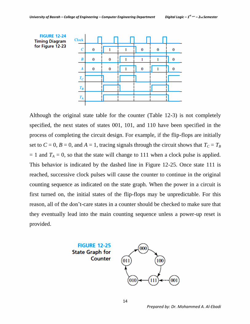
2. Counters for Other Sequences
In some applications, the sequence of states of a counter is not in straight binary
order. Figure 12-21 shows the state graph for such a counter. The arrows indicate
the state sequence. If this counter is started in state 000, the first clock pulse will
take it to state 100, the next pulse to 111, etc. The clock pulse is implicitly
understood to be the input to the circuit and not shown on the graph. The
corresponding state table for the counter is Table 12-3. Note that the next state is
unspecified for the present states 001, 101, and 110.
We will design the counter specified by Table 12-3 using T flip-flops. We could
derive TC, TB, and TA directly from this table, as in the preceding example. This
yields the maps and equations of Figure 12-22 and the circuit shown in Figure 12-
23.

University of Basrah – College of Engineering – Computer Engineering Department Digital Logic – 1st
year – 2nd Semester
13 Prepared by: Dr. Mohammed A. Al-Ebadi
The timing diagram of Figure 12-24, derived by tracing signals through the circuit,
verifies that the counter functions according to the state diagram of Figure 12-21;
for example, starting with CBA = 000, TC = 1 and TB = TA = 0. Therefore, when the
clock pulse comes along, only flip-flop C changes state, and the new state is
100.Then, TC = 0 and TB = TA = 1, so flip-flops B and A change state when the next
clock pulse occurs, etc. Note that the flip-flops change state following the falling
clock edge.
University of Basrah – College of Engineering – Computer Engineering Department Digital Logic – 1st
year – 2nd Semester
14 Prepared by: Dr. Mohammed A. Al-Ebadi
Although the original state table for the counter (Table 12-3) is not completely
specified, the next states of states 001, 101, and 110 have been specified in the
process of completing the circuit design. For example, if the flip-flops are initially
set to C = 0, B = 0, and A = 1, tracing signals through the circuit shows that TC = TB
= 1 and TA = 0, so that the state will change to 111 when a clock pulse is applied.
This behavior is indicated by the dashed line in Figure 12-25. Once state 111 is
reached, successive clock pulses will cause the counter to continue in the original
counting sequence as indicated on the state graph. When the power in a circuit is
first turned on, the initial states of the flip-flops may be unpredictable. For this
reason, all of the don’t-care states in a counter should be checked to make sure that
they eventually lead into the main counting sequence unless a power-up reset is
provided.

University of Basrah – College of Engineering – Computer Engineering Department Digital Logic – 1st
year – 2nd Semester
15 Prepared by: Dr. Mohammed A. Al-Ebadi
Counter Design Using D Flip-Flops
For a D flip-flop, Q+=D, so the D input map is identical with the next-state map.
Therefore, the equation for D can be read directly from the Q+
map. For the counter
of Figure 12-21, the following equations can be read from the next-state maps
shown in Figure 12-22(a):
This leads to the circuit shown in Figure 12-26 using D flip-flops. Note that the
connecting wires between the flip-flop outputs and the gate inputs have been
omitted to facilitate reading the diagram.
Counter Design Using S-R and J-K Flip-Flops
The procedures used to design a counter with S-R flip-flops are similar to the
procedures discussed for designing a counter using T and D flip-flops. However,
instead of deriving an input equation for each D or T flip-flop, the S and R input
equations must be derived.
Table 12-5(a) describes the behavior of the S-R flip-flop. Given S,R, and Q, we
can determine Q_ from this table.

University of Basrah – College of Engineering – Computer Engineering Department Digital Logic – 1st
year – 2nd Semester
16 Prepared by: Dr. Mohammed A. Al-Ebadi
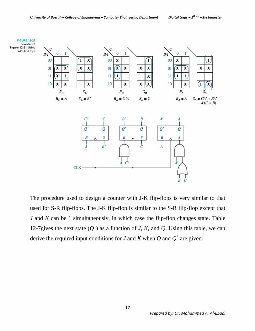
We will redesign the counter of Figure 12-21 using S-R flip-flops. Table 12-3 is
repeated in Table 12-6 with columns added for the S and R flip-flop inputs. These
columns can be filled in using Table 12-5(c). For CBA = 000, C = 0 and C+ = 1, so
SC = 1, RC = 0. For CBA = 010 and 011, C = 0 and C+ = 0, so SC = 0 and RC = X.
For CBA = 100, C = 1 and C+ = 1, so SC = X and RC = 0. For row 111, C = 1 and C
+
= 0, so SC = 0 and RC = l. For CBA = 001, 101, and 110, C+ = X, so SC = RC = X.
Similarly, the values of SB and RB are derived from the values of B and B+, and SA
and RA are derived from A and A+. The Karnaugh map of flip-flop input and the
resulting logic circuit for the counter are illustrated in Figure 12-27.
University of Basrah – College of Engineering – Computer Engineering Department Digital Logic – 1st
year – 2nd Semester
17 Prepared by: Dr. Mohammed A. Al-Ebadi
The procedure used to design a counter with J-K flip-flops is very similar to that
used for S-R flip-flops. The J-K flip-flop is similar to the S-R flip-flop except that
J and K can be 1 simultaneously, in which case the flip-flop changes state. Table
12-7gives the next state (Q+) as a function of J, K, and Q. Using this table, we can
derive the required input conditions for J and K when Q and Q+ are given.

University of Basrah – College of Engineering – Computer Engineering Department Digital Logic – 1st
year – 2nd Semester
18 Prepared by: Dr. Mohammed A. Al-Ebadi
We will now redesign the counter of Figure 12-21 using J-K flip-flops. Table 12-3
is repeated in Table 12-8 with columns added for the J and K flip-flop inputs. We
will fill in these columns using Table 12-7(c). For CBA = 000, C = 0 and C+ = 1, so
JC = 1 and KC = X. For CBA = 010 and 011, C = 0 and C+ = 0, so JC = 0 and KC =
X. The remaining table entries are filled in similarly. The Karnaugh map of flip-
flop input and the resulting logic circuit for the counter are illustrated in Figure 12-
28.

University of Basrah – College of Engineering – Computer Engineering Department Digital Logic – 1st
year – 2nd Semester
19 Prepared by: Dr. Mohammed A. Al-Ebadi