bimosfet in fly back
TRANSCRIPT

Technical Application Comparative Performance ofBIMOSFETs in Fly-Back
Converter Circuits
UDS
C1
IS D1
C2 U2
T1
U1
IS
0
t
tT
UDS
0tT
U1
Micro Controller
AC
U
V
W
DC
AC
Inverter
IGBT Driver
Brake Chopper
BIMOSFET
DC 1
DC 2
DC n
.
.
.
Inrush Current Limitation
Start up Circuit& Driver
C 1
C 2
C 3
Input Rectifier
DC 1
DC 2
DC 3
DC 4
DC 5
DC - Bus 500-800 V
400 V3 ~
50 Hz
AC
DC 400 V3 ~
0-50 Hz
Flyback Operation
The Flyback Converter is one of the most simple convertertypes. The minimum configuration consists of only a switch, atransformer, a diode and two capacitors as shown in fig. 1. The
Flyback Application
One of the typical applications for a flyback converter is theauxiliary power supply for the IGBT gate driver in an inverter.This application has all the requirements, which can be fulfilledideally by a flyback converter.
One of the typical applications for a flyback converter is the auxiliary power supply for the IGBT gate driver in an inverter. Theessential requirement for a switch of a flyback converter in a drives inverter is a high breakdown voltage combined with fastswitching speed. To minimize the predominant switching losses, the switch-on and -off energies have to be low. The mainadvantage of the BIMOSFET lies first in its lower turn- on losses and secondarily in its lower conduction losses. A comparisonof the total energy losses between a MOSFET and a BIMOSFET results in 35 % less total losses for the BIMOSFET.
Figure 1: flyback
energy in this converter type is stored in the air gap of theferrite core. Primary current ramps up during the on state ofthe switch storing magnetic energy, which is then transferredto the output by the diodes when the switch turns off. The powerrange for this converter type is limited to approximately 300 W.
The advantages of this circuit are the very wide input-outputvoltage ratio and the feasibility of adding more secondarywindings to create multiple output voltages. Furthermore, it isadvantageous to have galvanic insulation between primary andsecondary side. The disadvantages are the high breakdownvoltage required for the switch and the RFI emission generatedby the air gap in the transformer. The flyback converter can notwork without load or closed regulation loop as otherwise theoutput voltage will exceed allowable limits.
Figure 2: inverter
The shaded area in fig. 2 shows a converter with the start-upcircuit as part of the drives inverter. The auxiliary power supplycan be built very cost effectively with relatively few elements.
Since the input voltage for the converter is the DC-power bus,there is a wide voltage variation. During the precharge of thebus capacitors, the power supply has to work properly with verylow DC-bus voltages, as well as under braking operation of themotor, when the bus voltage reaches high values up to 750 V.The output voltage can easily be regulated by varying thetransistor duty cycle.
All the insulated DC- outputs can be generated by adding moreseparated secondary windings. For example the 5 V supply forthe micro controller, ± 15 V for current sensors, a common +15Vsupply for the driver of the three lower IGBTs and three separa-te +15V supplies for the upper IGBT drivers.
2
Epitaxial IGBT crossection
5 10 15 20 25 300
1
2
3
4
5
6
7
8
9
10
V_GS=4 VV_GS=5 V
V_GS=6 VV_GS=15 V
V_DS [V]
I_D [A]
Mosfet 1500V, 2A: T_vj=125°C
0
5 10 15 20 25 300
1
2
3
4
5
6
7
8
9
10
V_GE=7VV_GE=9 V
V_GE=11 VV_GE=15 V
V_CE [V]
I_C [A]
0
IXBH9N160; T_vj=125°C
Requirements for the Switch
The essential requirement for a switch of a flyback converter ina drives inverter is a high breakdown voltage. In a flybackconverter the maximum voltage applied to the switch isapproximately two x the input voltage. Therefore, the minimumbreakdown voltage must be higher than 2 x Vin. For standardinverters for motor control used off mains of 400 V, the DC-busvoltage can reach up to 750 V in the motor braking mode ofoperation. Here a breakdown voltage of at least 1600 V isneeded.
Flyback converters normally run with switching frequenciesbetween 50 to 100 kHz. To minimize the predominant switchinglosses the switch-on and -off energies have to be low. To achievethis, a high switching speed by the switch is obvious. A commontrick to avoid switch-on losses in a fly back topology is not toturn on the transistor until the current in the output diode hasreached zero (discontinuous mode). There must be a deadtimeuntil the next cycle starts. The advantage here is less transistorand diode commutation losses, which allows higher switchingfrequency in order to reduce the size of the transformer.
BIMOSFETTM Chip Technology
Standard high voltage IGBTs are too slow for flybackapplications. The new family of high voltage BIMOSFETtransistors is fulfilling these needs.
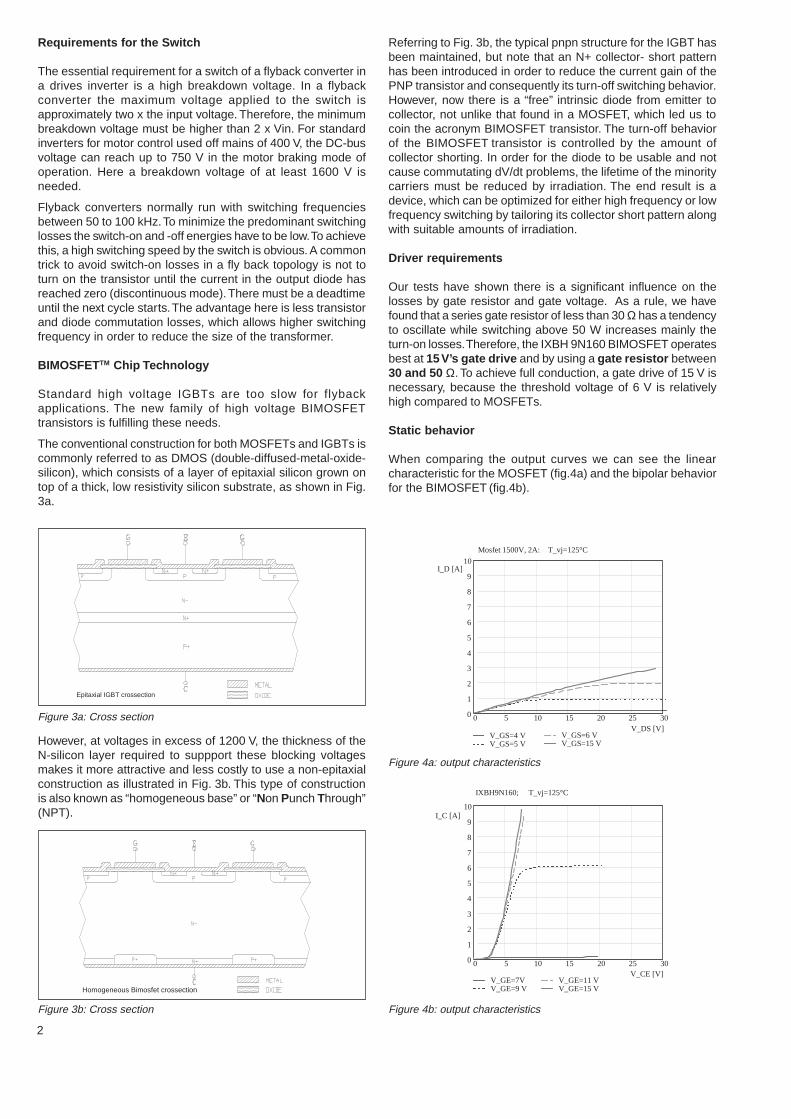
The conventional construction for both MOSFETs and IGBTs iscommonly referred to as DMOS (double-diffused-metal-oxide-silicon), which consists of a layer of epitaxial silicon grown ontop of a thick, low resistivity silicon substrate, as shown in Fig.3a.
Referring to Fig. 3b, the typical pnpn structure for the IGBT hasbeen maintained, but note that an N+ collector- short patternhas been introduced in order to reduce the current gain of thePNP transistor and consequently its turn-off switching behavior.However, now there is a “free” intrinsic diode from emitter tocollector, not unlike that found in a MOSFET, which led us tocoin the acronym BIMOSFET transistor. The turn-off behaviorof the BIMOSFET transistor is controlled by the amount ofcollector shorting. In order for the diode to be usable and notcause commutating dV/dt problems, the lifetime of the minoritycarriers must be reduced by irradiation. The end result is adevice, which can be optimized for either high frequency or lowfrequency switching by tailoring its collector short pattern alongwith suitable amounts of irradiation.
Driver requirements
Our tests have shown there is a significant influence on thelosses by gate resistor and gate voltage. As a rule, we havefound that a series gate resistor of less than 30 Ω has a tendencyto oscillate while switching above 50 W increases mainly theturn-on losses. Therefore, the IXBH 9N160 BIMOSFET operatesbest at 15 V’s gate drive and by using a gate resistor between30 and 50 Ω. To achieve full conduction, a gate drive of 15 V isnecessary, because the threshold voltage of 6 V is relativelyhigh compared to MOSFETs.
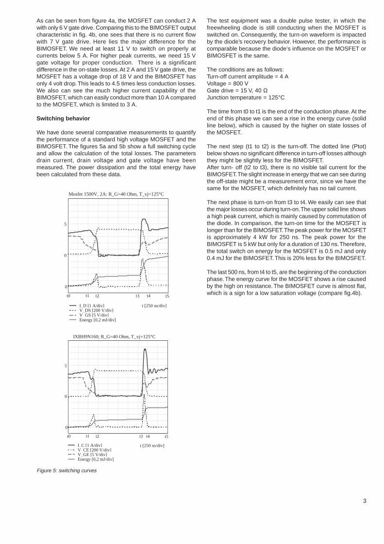
Static behavior
When comparing the output curves we can see the linearcharacteristic for the MOSFET (fig.4a) and the bipolar behaviorfor the BIMOSFET (fig.4b).
However, at voltages in excess of 1200 V, the thickness of theN-silicon layer required to suppport these blocking voltagesmakes it more attractive and less costly to use a non-epitaxialconstruction as illustrated in Fig. 3b. This type of constructionis also known as “homogeneous base” or “Non Punch Through”(NPT).
Figure 3a: Cross section
Homogeneous Bimosfet crossection
Figure 3b: Cross section Figure 4b: output characteristics
Figure 4a: output characteristics
3
0
0
5
I_D [1 A/div]V_DS [200 V/div]V_GS [5 V/div]Energy [0,2 mJ/div]
Mosfet 1500V, 2A: R_G=40 Ohm, T_vj=125°C
t [250 ns/div]
t1 t2 t3 t4t0 t5
0
0
5
I_C [1 A/div]V_CE [200 V/div]V_GE [5 V/div]Energy [0,2 mJ/div]
IXBH9N160; R_G=40 Ohm, T_vj=125°C
t [250 ns/div]
t1 t2 t3 t4t0 t5
As can be seen from figure 4a, the MOSFET can conduct 2 Awith only 6 V gate drive. Comparing this to the BIMOSFET outputcharacteristic in fig. 4b, one sees that there is no current flowwith 7 V gate drive. Here lies the major difference for theBIMOSFET. We need at least 11 V to switch on properly atcurrents below 5 A. For higher peak currents, we need 15 Vgate voltage for proper conduction. There is a significantdifference in the on-state losses. At 2 A and 15 V gate drive, theMOSFET has a voltage drop of 18 V and the BIMOSFET hasonly 4 volt drop. This leads to 4.5 times less conduction losses.We also can see the much higher current capability of theBIMOSFET, which can easily conduct more than 10 A comparedto the MOSFET, which is limited to 3 A.
Switching behavior
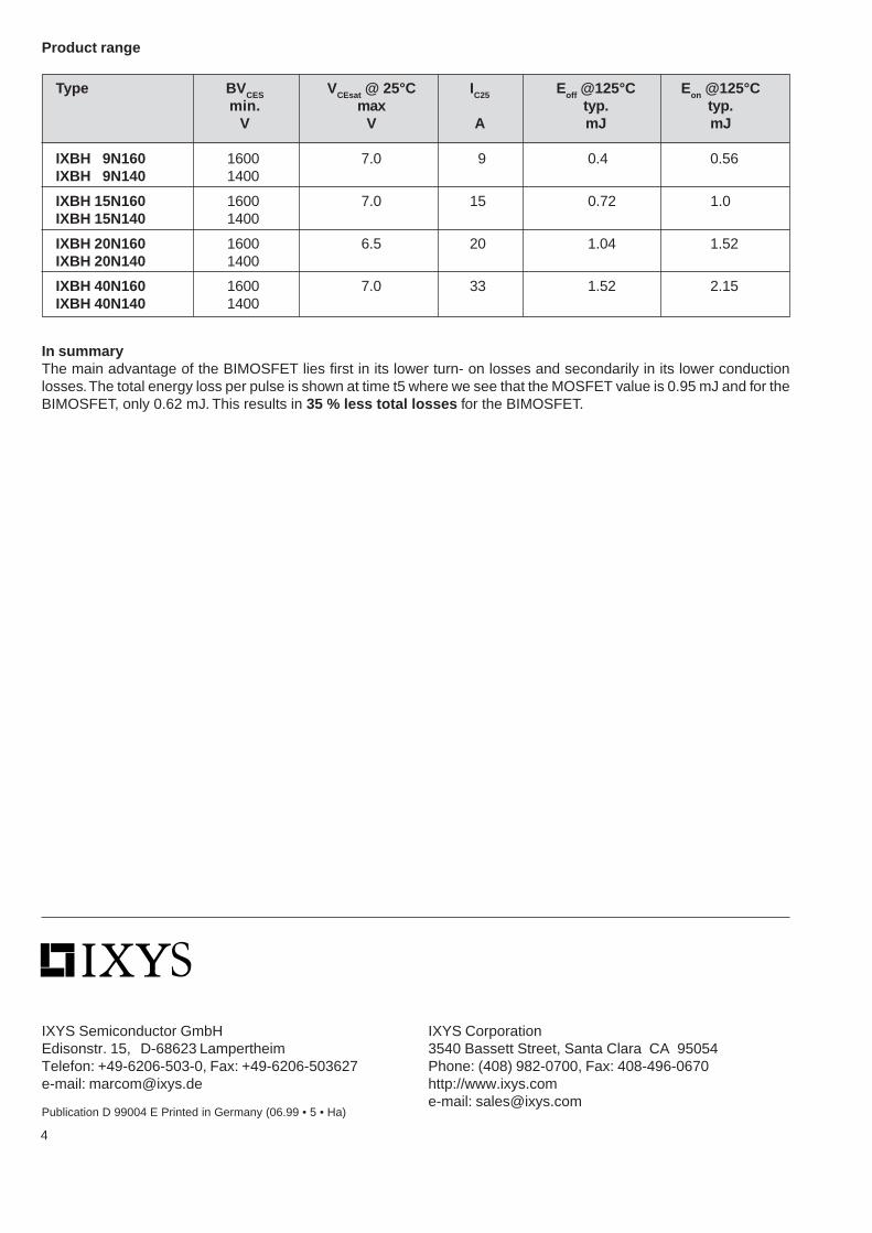
We have done several comparative measurements to quantifythe performance of a standard high voltage MOSFET and theBIMOSFET. The figures 5a and 5b show a full switching cycleand allow the calculation of the total losses. The parametersdrain current, drain voltage and gate voltage have beenmeasured. The power dissipation and the total energy havebeen calculated from these data.
The test equipment was a double pulse tester, in which thefreewheeling diode is still conducting when the MOSFET isswitched on. Consequently, the turn-on waveform is impactedby the diode’s recovery behavior. However, the performance iscomparable because the diode‘s influence on the MOSFET orBIMOSFET is the same.
The conditions are as follows:Turn-off current amplitude = 4 AVoltage = 800 VGate drive = 15 V, 40 ΩJunction temperature = 125°C
The time from t0 to t1 is the end of the conduction phase. At theend of this phase we can see a rise in the energy curve (solidline below), which is caused by the higher on state losses ofthe MOSFET.
The next step (t1 to t2) is the turn-off. The dotted line (Ptot)below shows no significant difference in turn-off losses althoughthey might be slightly less for the BIMOSFET.After turn- off (t2 to t3), there is no visible tail current for theBIMOSFET. The slight increase in energy that we can see duringthe off-state might be a measurement error, since we have thesame for the MOSFET, which definitely has no tail current.
The next phase is turn-on from t3 to t4. We easily can see thatthe major losses occur during turn-on. The upper solid line showsa high peak current, which is mainly caused by commutation ofthe diode. In comparison, the turn-on time for the MOSFET islonger than for the BIMOSFET. The peak power for the MOSFETis approximately 4 kW for 250 ns. The peak power for theBIMOSFET is 5 kW but only for a duration of 130 ns. Therefore,the total switch on energy for the MOSFET is 0.5 mJ and only0.4 mJ for the BIMOSFET. This is 20% less for the BIMOSFET.
The last 500 ns, from t4 to t5, are the beginning of the conductionphase. The energy curve for the MOSFET shows a rise causedby the high on resistance. The BIMOSFET curve is almost flat,which is a sign for a low saturation voltage (compare fig.4b).
Figure 5: switching curves
4
Product range
Type BV CES VCEsat @ 25°C IC25 Eoff @125°C Eon @125°Cmin. max typ. typ.
V V A mJ mJ
IXBH 9N160 1600 7.0 9 0.4 0.56IXBH 9N140 1400
IXBH 15N160 1600 7.0 15 0.72 1.0IXBH 15N140 1400
IXBH 20N160 1600 6.5 20 1.04 1.52IXBH 20N140 1400
IXBH 40N160 1600 7.0 33 1.52 2.15IXBH 40N140 1400
IXYS Semiconductor GmbHEdisonstr. 15, D-68623 LampertheimTelefon: +49-6206-503-0, Fax: +49-6206-503627e-mail: [email protected]
IXYS Corporation3540 Bassett Street, Santa Clara CA 95054Phone: (408) 982-0700, Fax: 408-496-0670http://www.ixys.come-mail: [email protected]
Publication D 99004 E Printed in Germany (06.99 • 5 • Ha)
In summaryThe main advantage of the BIMOSFET lies first in its lower turn- on losses and secondarily in its lower conductionlosses. The total energy loss per pulse is shown at time t5 where we see that the MOSFET value is 0.95 mJ and for theBIMOSFET, only 0.62 mJ. This results in 35 % less total losses for the BIMOSFET.