bcd smart power roadmap trends and challenges · bcd smart power roadmap trends and challenges ......
TRANSCRIPT
BCD Smart Power RoadmapTrends and ChallengesGiuseppe Croce
NEREID WORKSHOP ‘Smart Energy’
Bertinoro, October 20 th
Outline
• Introduction
• Major Trends in Smart Power ASICs
• An insight on (some) differentiating enablers• Power Devices evolution
• Enhanced Programmability (ePCM)
• High Voltage applications
• Challenges & Conclusions
2
Outline
• Introduction
• Major Trends in Smart Power ASICs
• An insight on (some) differentiating enablers• Power Devices evolution
• Enhanced Programmability (ePCM)
• High Voltage applications
• Challenges & Conclusions
3
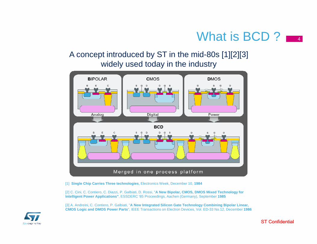
What is BCD ?A concept introduced by ST in the mid-80s [1][2][3]
widely used today in the industry
[1] Single Chip Carries Three technologies , Electronics Week, December 10, 1984
[2] C. Cini, C. Contiero, C. Diazzi, P. Galbiati, D. Rossi, "A New Bipolar, CMOS, DMOS Mixed Technology for Intelligent Power Applications" , ESSDERC '85 Proceedings, Aachen (Germany), September 1985
[3] A. Andreini, C. Contiero, P. Galbiati, "A New Integrated Silicon Gate Technology Combining Bipolar Linear, CMOS Logic and DMOS Power Parts ", IEEE Transactions on Electron Devices, Vol. ED-33 No.12, December 1986
4
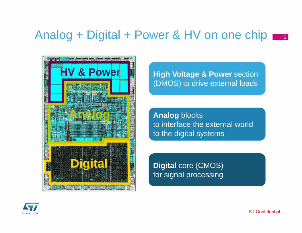
Analog + Digital + Power & HV on one chip
High Voltage & Power section (DMOS) to drive external loads
Digital core (CMOS)for signal processing
Analog blocksto interface the external worldto the digital systems
HV & Power
Analog
Digital
5
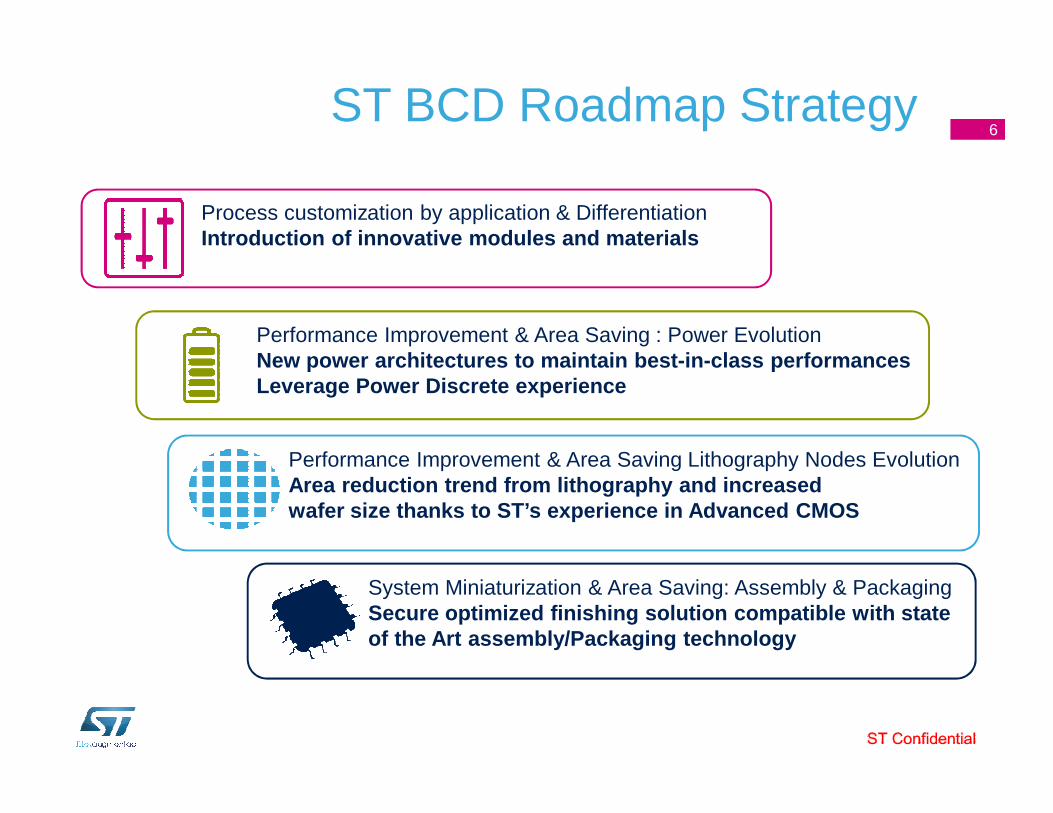
ST BCD Roadmap Strategy
Performance Improvement & Area Saving Lithography Nodes Evolution Area reduction trend from lithography and increased wafer size thanks to ST’s experience in Advanced CM OS
Performance Improvement & Area Saving : Power EvolutionNew power architectures to maintain best-in-class p erformancesLeverage Power Discrete experience
Process customization by application & DifferentiationIntroduction of innovative modules and materials
System Miniaturization & Area Saving: Assembly & PackagingSecure optimized finishing solution compatible with state of the Art assembly/Packaging technology
6
Outline
• Introduction
• Major Trends in Smart Power ASICs
• An insight on (some) differentiating enablers• Power Devices evolution
• Enhanced Programmability (ePCM)
• High Voltage applications
• Challenges & Conclusions
7
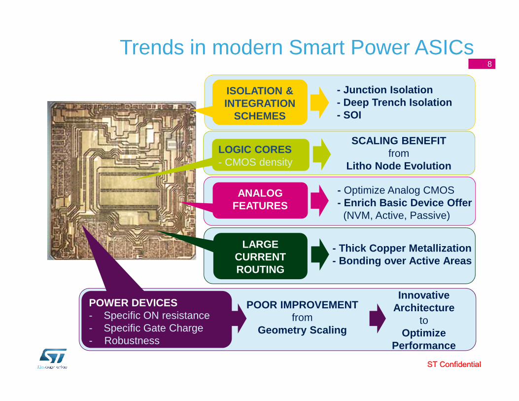
Trends in modern Smart Power ASICs
LOGIC CORES- CMOS density
SCALING BENEFITfrom
Litho Node Evolution
8
POWER DEVICES- Specific ON resistance- Specific Gate Charge- Robustness
POOR IMPROVEMENTfrom
Geometry Scaling
Innovative Architecture
toOptimize
Performance
ISOLATION &INTEGRATION
SCHEMES
- Junction Isolation- Deep Trench Isolation- SOI
ANALOGFEATURES
- Optimize Analog CMOS- Enrich Basic Device Offer
(NVM, Active, Passive)
LARGECURRENTROUTING
- Thick Copper Metallization- Bonding over Active Areas
Cu-Damascene + Al-cap
METAL3
Al-cap (Pad finishing)
Al
AuWIRE
Cu
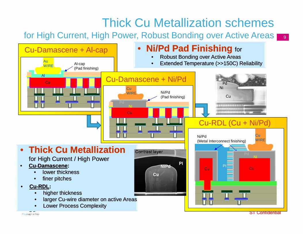
• Thick Cu Metallizationfor High Current / High Power
• Cu-Damascene:• lower thickness• finer pitches
• Thick Cu Metallizationfor High Current / High Power
• Cu-Damascene:• lower thickness• finer pitches
Thick Cu Metallization schemesfor High Current, High Power, Robust Bonding over Active Areas
• Ni/Pd Pad Finishing for• Robust Bonding over Active Areas• Extended Temperature (>>150C) Reliability
• Ni/Pd Pad Finishing for• Robust Bonding over Active Areas• Extended Temperature (>>150C) Reliability
METAL3
CuWIRE
Cu-Damascene + Ni/Pd
Ni/Pd(Pad finishing)
Cu
PdNi
Cu
Ni
Pd
9
• Cu-RDL:• higher thickness• larger Cu-wire diameter on active Areas• Lower Process Complexity
• Cu-RDL:• higher thickness• larger Cu-wire diameter on active Areas• Lower Process Complexity
Cu-RDL (Cu + Ni/Pd)
Ni/Pd(Metal Interconnect finishing)
Cu
CuWIRE
Cu
NiPd
PI
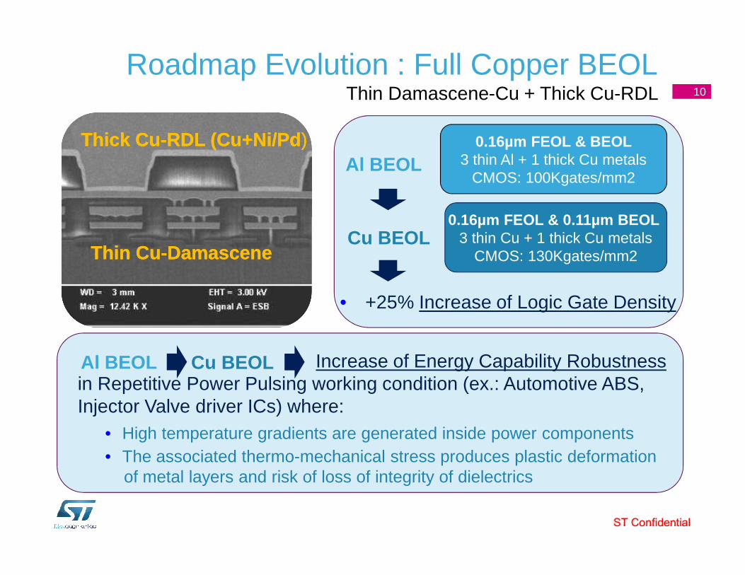
Roadmap Evolution : Full Copper BEOLThin Damascene-Cu + Thick Cu-RDL
Thick Cu-RDL (Cu+Ni/Pd )Thick Cu-RDL (Cu+Ni/Pd )
Thin Cu-DamasceneThin Cu-Damascene
Increase of Energy Capability Robustnessin Repetitive Power Pulsing working condition (ex.: Automotive ABS, Injector Valve driver ICs) where:
• High temperature gradients are generated inside power components• The associated thermo-mechanical stress produces plastic deformation
of metal layers and risk of loss of integrity of dielectrics
Al BEOL Cu BEOL
0.16µm FEOL & BEOL3 thin Al + 1 thick Cu metals
CMOS: 100Kgates/mm2
0.16µm FEOL & 0.11µm BEOL 3 thin Cu + 1 thick Cu metals
CMOS: 130Kgates/mm2
Al BEOL
Cu BEOL
• +25% Increase of Logic Gate Density
10
Outline
• Introduction
• Major Trends in Smart Power ASICs
• An insight on (some) differentiating enablers• Power Devices evolution
• Enhanced Programmability (ePCM)
• High Voltage applications
• Challenges & Conclusions
11
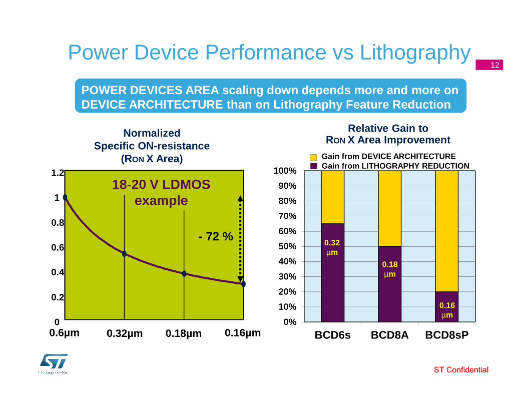
Power Device Performance vs Lithography 12
0%
10%
20%
30%
40%
50%
60%
70%
80%
90%
100%
BCD6s BCD8A BCD8sP
Relative Gain toRON X Area Improvement
0.16µm
0.18µm
0.32µm
Gain from DEVICE ARCHITECTUREGain from LITHOGRAPHY REDUCTION
POWER DEVICES AREA scaling down depends more and mo re on DEVICE ARCHITECTURE than on Lithography Feature Red uction
0.6µm 0.32µm 0.18µm0
0.2
0.4
0.6
0.8
1
1.2
0.16µm
- 72 %
18-20 V LDMOS example
NormalizedSpecific ON-resistance
(RON X Area)
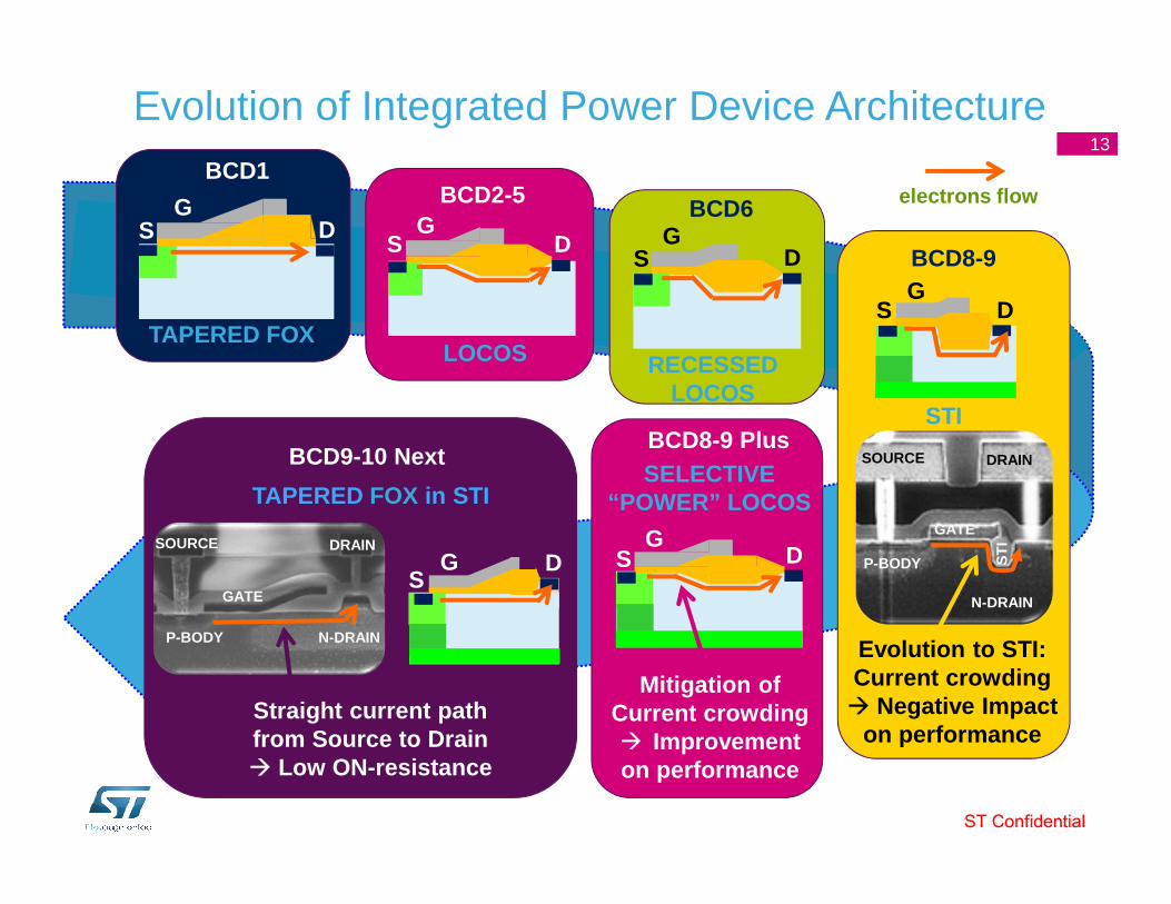
Evolution of Integrated Power Device Architecture
electrons flow
S DG
BCD1
TAPERED FOX
S DG
BCD2-5
LOCOS
S DG
BCD6
RECESSEDLOCOS
13
Evolution to STI:Current crowding� Negative Impact
on performance
BCD8-9
S DG
STI
ST
I
GATE
SOURCE DRAIN
P-BODY
N-DRAIN
BCD8-9 Plus
S DG
SELECTIVE“POWER” LOCOS
Mitigation ofCurrent crowding� Improvementon performance
BCD9-10 Next
TAPERED FOX in STI
SDG
Straight current path from Source to Drain� Low ON-resistance
GATE
SOURCE DRAIN
P-BODY N-DRAIN
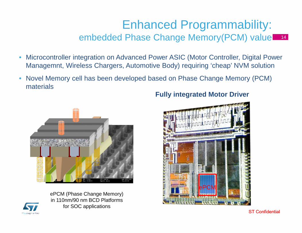
Fully integrated Motor Driver
Enhanced Programmability:embedded Phase Change Memory(PCM) value
• Microcontroller integration on Advanced Power ASIC (Motor Controller, Digital Power Managemnt, Wireless Chargers, Automotive Body) requiring ‘cheap’ NVM solution
• Novel Memory cell has been developed based on Phase Change Memory (PCM) materials
14
GST
ePCM (Phase Change Memory)in 110nm/90 nm BCD Platforms
for SOC applications
ePCM
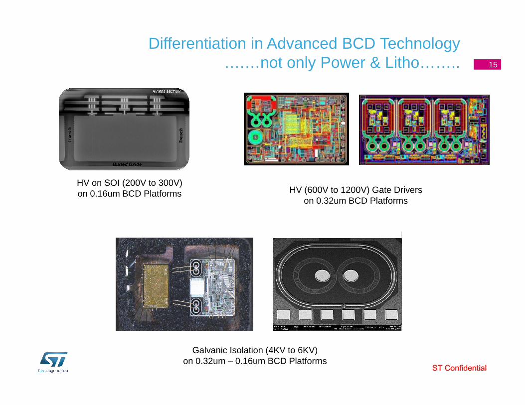
Differentiation in Advanced BCD Technology….…not only Power & Litho…….. 15
HV (600V to 1200V) Gate Driverson 0.32um BCD Platforms
Galvanic Isolation (4KV to 6KV)on 0.32um – 0.16um BCD Platforms
HV on SOI (200V to 300V)on 0.16um BCD Platforms
Outline
• Introduction
• Major Trends in Smart Power ASICs
• An insight on (some) differentiating enablers• Power Devices evolution
• Enhanced Programmability (ePCM)
• High Voltage applications
• Challenges & Conclusions
16
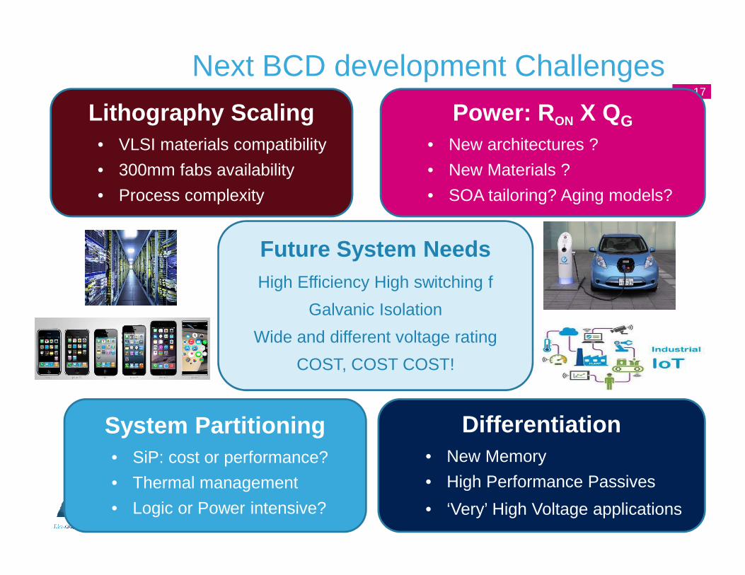
Next BCD development Challenges17
Lithography Scaling• VLSI materials compatibility
• 300mm fabs availability
• Process complexity
Power: R ON X QG
• New architectures ?
• New Materials ?
• SOA tailoring? Aging models?
System Partitioning• SiP: cost or performance?
• Thermal management
• Logic or Power intensive?
Differentiation• New Memory
• High Performance Passives
• ‘Very’ High Voltage applications
Future System NeedsHigh Efficiency High switching f
Galvanic Isolation
Wide and different voltage rating
COST, COST COST!
Conclusions
• Smart Power BCD Technology is ‘slowly’ evolving to wards Advanced CMOS Platforms
• Process customization and differentiation are key t o boost technology platform competitiveness
• New Specific Modules (Cu RDL and DTI) in volume pr oduction• New Power device architecture as cost redution ena bler and to meet high efficiency/
high frequency Power management• New features availability to enable new function in tegration
18
1/10/2017