basic isolated three-phase compact power stage ref design
TRANSCRIPT

White
ISO53X0XDWVISO53X0XDWV
NTC
UCC5350M orUCC5390E
ISO53X0XDWVISO53X0XDWVUCC5350M orUCC5390E
PWM_TOP_X
PWM_BOT_X
UV
W
Six Pack IGBT Module
x3
x3
VDC+
VDC-
AMC1306
Current Sense (only one phase shown)
AMC1306AMC1306
DC Bus Voltage Sense Temperature Sense
TLV521
Delfino Control Card
SN74LVC1G17
TLV1117-33
Clock Buffer
LM3480IM3-5.0 TLV70433
x2
15V_TOP_X
5V_X
x2
x2
15V_BOT
3.3V_SEC
5V_X
3.3V_PRI5V_PRICLK
CLK_MCU
TIDA-01420
Current Sensex3
PWM_TOP_X
x3
PWM_BOT_X
x2
CLKCLK
CLK
ACIM
Copyright © 2017, Texas Instruments Incorporated
Narrow body SOIC (4 mm) Basic isolated gate drivers
1TIDUDG6–September 2017Submit Documentation Feedback
Copyright © 2017, Texas Instruments Incorporated
Basic Isolated Three-Phase Compact Power Stage Reference Design forIndustrial Drives
TI Designs: TIDA-01420Basic Isolated Three-Phase Compact Power StageReference Design for Industrial Drives
DescriptionThis three-phase, compact power stage referencedesign uses a gate driver with basic isolation(UCC53xx) to cater to the isolation requirements ofsystems using dual controllers. The capacitive isolationof the gate driver offers a longer lifetime and betterpropagation delay match over optocouplers tominimize the inverter deadband distortions and losses.If required, another level of basic isolation can be usedbetween the controllers to achieve reinforced isolationat the system level. This approach optimizes theisolation cost of the system as well as helps achievecompactness. This design also demonstrates theinterlocking feature of the UCC53xx gate driver, whichprotects the IGBTs during shoot-through. Thisreference design uses the F28379D Delfino™ controlcard to generate PWM signals for controlling the three-phase inverter.
Resources
TIDA-01420 Design FolderUCC5350MCD Product FolderUCC5390ECD Product FolderLM3480 Product FolderTLV704 Product FolderTLV1117-33 Product FolderSN74LVC1G17 Product FolderTMDSCNCD28379D Tool Folder
ASK Our E2E Experts
Features• Basic Isolated 200- to 480-V AC Three-Phase
Power Stage With Direct PWM CMOS Interface toMCU for Hot-Side Control
• Low Pin Count Gate Driver UCC53xx EnablesCompact Solution and Increased Flexibility of GateDriver Placement
• Short (72 ns Typical) Propagation Delay and VerySmall Skew Between Propagation DelaysOptimizes Deadband Distortion and Losses
• Gate Driver Supports Option for PWM InterlockProtection to Avoid Shoot-Through
• Option to Populate Three Variants of Gate Drivers:Miller Clamp to Avoid Parasitic Turnon Effect;UVLO With Reference to Emitter to Provide RobustProtection of IGBT Against Operation in LinearRegion; and Split Output to Control Rise and FallTimes
• Built-in Bootstrap-Based Unipolar Power Supply forHigh-Side Drivers and Option to Feed ExternalBipolar Voltage Rails
• Gate Driver With High Drive Strength of 17-ASink/Source Currents Enables Driving High-CurrentIGBTs Without External Buffer
Applications• AC Inverter and VF Drives• Industrial Power Supplies• Servo Drives• Solar inverters
1
2
3
C
+L
+
-
+
-
+
-
Motor
-
Input Converter (Diode Bridge)
DC Bus (Filter)
Output Inverter (,*%7¶V)
+
-
+
-
System Description www.ti.com
2 TIDUDG6–September 2017Submit Documentation Feedback
Copyright © 2017, Texas Instruments Incorporated
Basic Isolated Three-Phase Compact Power Stage Reference Design forIndustrial Drives
An IMPORTANT NOTICE at the end of this TI reference design addresses authorized use, intellectual property matters and otherimportant disclaimers and information.
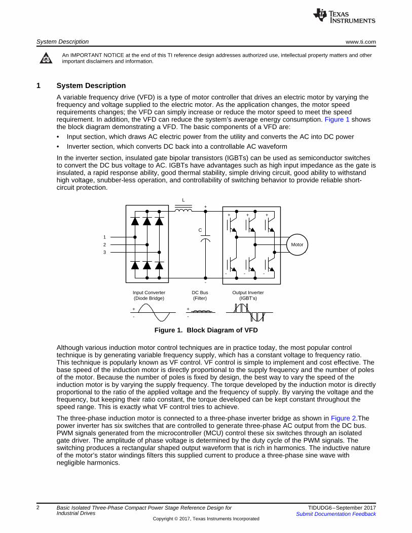
1 System DescriptionA variable frequency drive (VFD) is a type of motor controller that drives an electric motor by varying thefrequency and voltage supplied to the electric motor. As the application changes, the motor speedrequirements changes; the VFD can simply increase or reduce the motor speed to meet the speedrequirement. In addition, the VFD can reduce the system’s average energy consumption. Figure 1 showsthe block diagram demonstrating a VFD. The basic components of a VFD are:• Input section, which draws AC electric power from the utility and converts the AC into DC power• Inverter section, which converts DC back into a controllable AC waveform
In the inverter section, insulated gate bipolar transistors (IGBTs) can be used as semiconductor switchesto convert the DC bus voltage to AC. IGBTs have advantages such as high input impedance as the gate isinsulated, a rapid response ability, good thermal stability, simple driving circuit, good ability to withstandhigh voltage, snubber-less operation, and controllability of switching behavior to provide reliable short-circuit protection.
Figure 1. Block Diagram of VFD
Although various induction motor control techniques are in practice today, the most popular controltechnique is by generating variable frequency supply, which has a constant voltage to frequency ratio.This technique is popularly known as VF control. VF control is simple to implement and cost effective. Thebase speed of the induction motor is directly proportional to the supply frequency and the number of polesof the motor. Because the number of poles is fixed by design, the best way to vary the speed of theinduction motor is by varying the supply frequency. The torque developed by the induction motor is directlyproportional to the ratio of the applied voltage and the frequency of supply. By varying the voltage and thefrequency, but keeping their ratio constant, the torque developed can be kept constant throughout thespeed range. This is exactly what VF control tries to achieve.
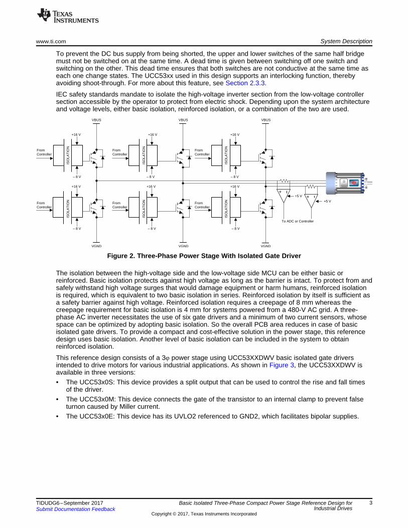
The three-phase induction motor is connected to a three-phase inverter bridge as shown in Figure 2.Thepower inverter has six switches that are controlled to generate three-phase AC output from the DC bus.PWM signals generated from the microcontroller (MCU) control these six switches through an isolatedgate driver. The amplitude of phase voltage is determined by the duty cycle of the PWM signals. Theswitching produces a rectangular shaped output waveform that is rich in harmonics. The inductive natureof the motor’s stator windings filters this supplied current to produce a three-phase sine wave withnegligible harmonics.
FromController
FromController
FromController
FromController
FromController
FromController
ISO
LAT
ION
ISO
LAT
ION
ISO
LAT
ION
ISO
LAT
ION
ISO
LAT
ION
ISO
LAT
ION
VBUS VBUS VBUS
VGND VGND VGND
+16 V +16 V +16 V
+16 V+16 V +16 V
+5 V
+5 V
± 8 V ± 8 V ± 8 V
To ADC or Controller
± 8 V ± 8 V ± 8 V
+
+
TI'DYH¶V
ControlCenter
www.ti.com System Description
3TIDUDG6–September 2017Submit Documentation Feedback
Copyright © 2017, Texas Instruments Incorporated
Basic Isolated Three-Phase Compact Power Stage Reference Design forIndustrial Drives
To prevent the DC bus supply from being shorted, the upper and lower switches of the same half bridgemust not be switched on at the same time. A dead time is given between switching off one switch andswitching on the other. This dead time ensures that both switches are not conductive at the same time aseach one change states. The UCC53xx used in this design supports an interlocking function, therebyavoiding shoot-through. For more about this feature, see Section 2.3.3.
IEC safety standards mandate to isolate the high-voltage inverter section from the low-voltage controllersection accessible by the operator to protect from electric shock. Depending upon the system architectureand voltage levels, either basic isolation, reinforced isolation, or a combination of the two are used.
Figure 2. Three-Phase Power Stage With Isolated Gate Driver
The isolation between the high-voltage side and the low-voltage side MCU can be either basic orreinforced. Basic isolation protects against high voltage as long as the barrier is intact. To protect from andsafely withstand high voltage surges that would damage equipment or harm humans, reinforced isolationis required, which is equivalent to two basic isolation in series. Reinforced isolation by itself is sufficient asa safety barrier against high voltage. Reinforced isolation requires a creepage of 8 mm whereas thecreepage requirement for basic isolation is 4 mm for systems powered from a 480-V AC grid. A three-phase AC inverter necessitates the use of six gate drivers and a minimum of two current sensors, whosespace can be optimized by adopting basic isolation. So the overall PCB area reduces in case of basicisolated gate drivers. To provide a compact and cost-effective solution in the power stage, this referencedesign uses basic isolation. Another level of basic isolation can be included in the system to obtainreinforced isolation.
This reference design consists of a 3φ power stage using UCC53XXDWV basic isolated gate driversintended to drive motors for various industrial applications. As shown in Figure 3, the UCC53XXDWV isavailable in three versions:• The UCC53x0S: This device provides a split output that can be used to control the rise and fall times
of the driver.• The UCC53x0M: This device connects the gate of the transistor to an internal clamp to prevent false
turnon caused by Miller current.• The UCC53x0E: This device has its UVLO2 referenced to GND2, which facilitates bipolar supplies.

1VCC1 8 VEE2
2IN+ 7 GND2
3IN± 6 OUT
4GND1 5 VCC2
Not to scale
1VCC1 8 VEE2
2IN+ 7 CLAMP
3IN± 6 OUT
4GND1 5 VCC2
Not to scale
1VCC1 8 VEE2
2IN+ 7 OUTL
3IN± 6 OUTH
4GND1 5 VCC2
Not to scale
UCC5320S and UCC5390S D Package8-Pin SOICTop View
UCC5310M and UCC5350M D Package8-Pin SOICTop View
UCC5320E and UCC5390E D Package8-Pin SOICTop View
Copyright © 2017, Texas Instruments Incorporated
System Description www.ti.com
4 TIDUDG6–September 2017Submit Documentation Feedback
Copyright © 2017, Texas Instruments Incorporated
Basic Isolated Three-Phase Compact Power Stage Reference Design forIndustrial Drives
Figure 3. Pin Diagram of UCC53xx
This reference design characterizes the Miller clamp and UVLO versions of the gate drivers using theUCC5350MCD and UCC5390ECD, respectively. The IGBTs used to test these gate drivers are as follows:• UCC5350MCD: CM100TX-24S• UCC5390ECD: 6MI180VB-120-50
www.ti.com System Description
5TIDUDG6–September 2017Submit Documentation Feedback
Copyright © 2017, Texas Instruments Incorporated
Basic Isolated Three-Phase Compact Power Stage Reference Design forIndustrial Drives
1.1 Key System Specifications
Table 1. Key System Specifications
PARAMETER SPECIFICATIONS DETAILS
DC link voltage 280- to 900-V DC
900-V DC max to provide margin for motorregeneration and boost PFC if used. 280- to
680-V DC corresponds to grid voltage of 200-to 480-V AC
IGBT module6MBI180VB-120-50, 1200-V DC, 150A 6MBI180VB-120-50 is used with UCC5390E
and CM100TX-24S is used with UCC5350MCM100TX-24S 1200-V DC, 100 A
Isolation Basic —Clearance 4 mm —Gate driver package 8 pin SOIC(D) —
Source/sink current rating (Minimum)UCC5390E: 12 Apk/12 Apk
—UCC5350M: 10 Apk/5 Apk
Switching frequency 4 to 16 kHz —
Dead time(minimum) 25 ns (gate driver max skew) + deadtime for specific IGBT module
Inverter tested with a 1-µs deadband; can bevaried as long as there is no overlap betweenVGE signals of top and bottom IGBT switches
PCB 4 layer, 1-oz copper, high Tg FR4, 1.6mm thick —
Primary side supply 5 V ± 5%, 500 mA —
Secondary side supplyUCC5390E: 15-V / -8 V bipolar
—UCC5350M: 15-V unipolar
PCB size 167 mm × 178 mm —PCB thickness 1.6 mm —
Ambient Temperature 0°C to 55°C
Components selected support the industrialtemperature range of 85°C and the reference
design can operate outside the mentionedtemperature range with sufficient derating.
Tested only from 0°C to 55°C
Microcontroller Interface
7 PWM signals, current sensemodulator bit streams for two motorphases, DC-link voltage sensemodulator bit stream, temperaturesense modulator bit stream, clocksignal, 5 V for the controller board
—
White
ISO53X0XDWVISO53X0XDWV
NTC
UCC5350M orUCC5390E
ISO53X0XDWVISO53X0XDWVUCC5350M orUCC5390E
PWM_TOP_X
PWM_BOT_X
UV
W
Six Pack IGBT Module
x3
x3
VDC+
VDC-
AMC1306
Current Sense (only one phase shown)
AMC1306AMC1306
DC Bus Voltage Sense Temperature Sense
TLV521
Delfino Control Card
SN74LVC1G17
TLV1117-33
Clock Buffer
LM3480IM3-5.0 TLV70433
x2
15V_TOP_X
5V_X
x2
x2
15V_BOT
3.3V_SEC
5V_X
3.3V_PRI5V_PRICLK
CLK_MCU
TIDA-01420
Current Sensex3
PWM_TOP_X
x3
PWM_BOT_X
x2
CLKCLK
CLK
ACIM
Copyright © 2017, Texas Instruments Incorporated
Narrow body SOIC (4 mm) Basic isolated gate drivers
System Overview www.ti.com
6 TIDUDG6–September 2017Submit Documentation Feedback
Copyright © 2017, Texas Instruments Incorporated
Basic Isolated Three-Phase Compact Power Stage Reference Design forIndustrial Drives
2 System OverviewThe UCC53xx isolated gate driver is available in an 8-pin SOIC (D) package. This package has acreepage and clearance of 4 mm and can support isolation voltage up to 3 kVRMS, which is good forapplications where basic isolation is needed. The maximum isolation working voltage (VIOWM) for theUCC53xx is 700 VRMS. The UCC53x0 family has lower part-to-part skew, lower propagation delay, higheroperating temperature, and higher common mode transient immunity (CMTI).
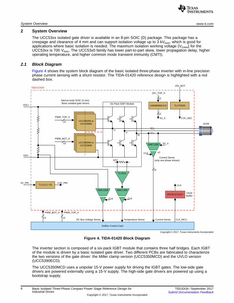
2.1 Block DiagramFigure 4 shows the system block diagram of the basic isolated three-phase inverter with in-line precisionphase current sensing with a shunt resistor. The TIDA-01420 reference design is highlighted with a reddashed box.
Figure 4. TIDA-01420 Block Diagram
The inverter section is composed of a six-pack IGBT module that contains three half bridges. Each IGBTof the module is driven by a basic isolated gate driver. Two different PCBs are fabricated to characterizethe two versions of the gate driver: the Miller clamp version (UCC5350MCD) and the UVLO version(UCC5390ECD).
The UCC5350MCD uses a unipolar 15-V power supply for driving the IGBT gates. The low-side gatedrivers are powered externally using a 15-V supply. The high-side gate drivers are powered up using abootstrap supply.

VCC1
IN+
IN-
GND1
VEE2
CLAMP
OUT
VCC2
VCC1
IN+
IN-
GND1
VEE2
CLAMP
OUT
VCC2
Microcontroller
PWM_HIGH
PWM_LOW
Input PWM
Negative dead time
Output of both drivers
is LOW
Output PWMVDC+
C
E
G
C
E
G
Copyright © 2017, Texas Instruments Incorporated
www.ti.com System Overview
7TIDUDG6–September 2017Submit Documentation Feedback
Copyright © 2017, Texas Instruments Incorporated
Basic Isolated Three-Phase Compact Power Stage Reference Design forIndustrial Drives
The UCC5390ECD uses a bipolar 15-V and –8-V power supply for driving the gates of the IGBTs. Thelow-side gate drivers are powered externally using a 15-V/–8-V single bipolar supply. The standardmethod for bootstrapping a positive gate voltage cannot be extended to negative voltages withoutincreasing the complexity. Therefore, in this reference design, the three high-side gate drivers arepowered externally using three different power supplies.
A primary-side 3.3-V supply is derived from the 5-V input through the LDO regulator TLV1117-33. ThePWM input signals for the gate drivers are routed to a D-SUB 25-pin female connector, which isconnected to the Delfino control card TMDSCNCD28379D through an adapter board. Interlocking ispresent as an optional protection feature in this design at the input of the gate driver. When single gatedrivers are used in half-bridge configuration, they usually allow cross conduction instead of preventing it incase of wrong input signals coming from the controller device. This limitation is due to the fact that eachdriver does not have the possibility to know the status of the input signal of the other companion driver inthe same leg. The availability of two input pins with opposite polarity allows implementing an hardwareinterlocking that prevents cross conduction even in case of wrong input signals generated by the controlunit. This can be achieved by making connections as shown in Figure 5.
Figure 5. Hardware Cross-Connection Prevention Using Interlocking
The output of the gate driver is connected to the gate of the IGBT through an external resistor, which cancontrol the source and sink currents provided by the gate driver.
2.2 Highlighted Products
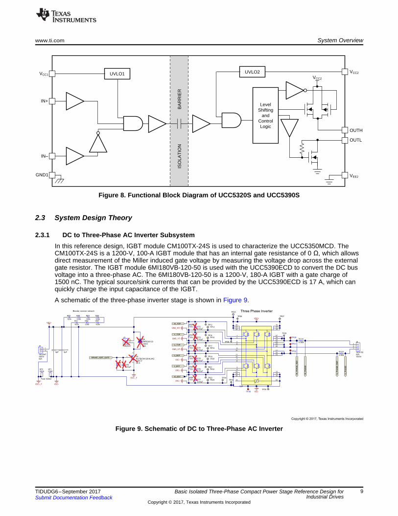
2.2.1 UCC5350M and UCC5390EThe UCC53xx is a family of compact, single-channel, isolated IGBT, SiC and MOSFET gate drivers withsuperior isolation ratings and includes variants for pinout configuration, drive strength, and package. TheUCC53xxMCD option connects the gate to an internal clamp to prevent false turnon caused by Millercurrent. The UCC53xxECD option has its UVLO2 referenced to GND2; it is recommended to connect thispin to the IGBT emitter. Compared to an optocoupler, the UCC53xx family has superior insulation voltage,lower power consumption, quiescent current, and CMTI. Figure 6, Figure 7, and Figure 8 show thefunctional block diagrams of UCC5390ECD and UCC5350MCD. Table 2 shows the drive strengthcapabilities of different gate drivers.

VEE2
VCC2
Level Shifting
andControl Logic
UVLO2UVLO1
GND1
VCC1
IN±
IN+
OUT
CLAMP
2 V
ISO
LAT
ION
BA
RR
IER
VCC2
VEE2
VCC2
Level Shifting
andControl Logic
UVLO2UVLO1
GND1
VCC1
IN±
IN+
VCC2
OUT
GND2ISO
LAT
ION
BA
RR
IER
System Overview www.ti.com
8 TIDUDG6–September 2017Submit Documentation Feedback
Copyright © 2017, Texas Instruments Incorporated
Basic Isolated Three-Phase Compact Power Stage Reference Design forIndustrial Drives
Table 2. Drive Strength Capabilities of Different Versions of UCC53xx
PART NUMBER MINIMUM SOURCE AND SINK CURRENT DESCRIPTIONUCC5310M 2.4 A and 1.1 A Miller clampUCC5320S 2.4 A and 2.2 A Split outputUCC5320E 2.4 A and 2.2 A A UVLO with respect to IGBT emitterUCC5350M 5 A and 5 A Miller clampUCC5390S 10 A and 10 A Split outputUCC5390E 10 A and 10 A A UVLO with respect to IGBT emitter
Figure 6. Functional Block Diagram of UCC5320E and UCC5390E
Figure 7. Functional Block Diagram of UCC5310M and UCC5350M
W_
PH
AS
E
Three Phase Inverter
U_
PH
AS
E
U_
PH
AS
E_R
EF
10kR20
10kR96
W_TOP
GND_WT
10kR26
10kR112
10kR12
10kR38
10k
R32V_TOP
GND_VT
U_TOP
GND_UT
W_BOT
VDC-
V_BOT
VDC-
U_BOT
VDC-
1
2
32A1000V
J8
1902547
1200V30A
D9RHRG30120
0.01µFC78
1
2
3
32A
1000V
J4
1904150
0.01µFC72
0.01µFC73
0.01µFC74
0.01µFC75
0.01µFC76
0.01µFC77
TP17TP18
TP19TP20
TP21TP22
TP23TP24
TP14TP16
TP12TP13
TP28
TP30
VDC+
VDC+TP27TP26
TP33
VDC-
0.004
R118
0.004
R120
TP25
TP36
W_
PH
AS
E_R
EF
3
1
2
1200 V50 A
Q1NGTB25N120IHLWG
BRAKE_IGBT_GATE
3µFC112
3µFC111
1
2
J3
1902547
1
2
3
4
27
28
29
5
6
7
8
24
25
26
9
10
11
12
21
22
23
13
1630
33
15
1832
35
14
1731
34
19 20
U24
TP29
TP31
TP32
TP34
TP35
XF13566
XF23566
VDC-
Fuse holder
100k
R45
100k
R48
100k
R49
100k
R51
100k
R54
100k
R57100k
R50
Bleeder resistor network
VDC-_F
VDC-_F
Copyright © 2017, Texas Instruments Incorporated
VEE2
VCC2
Level Shifting
andControl Logic
UVLO2UVLO1
GND1
VCC1
IN±
IN+
VCC2
OUTH
ISO
LAT
ION
BA
RR
IER
OUTL
www.ti.com System Overview
9TIDUDG6–September 2017Submit Documentation Feedback
Copyright © 2017, Texas Instruments Incorporated
Basic Isolated Three-Phase Compact Power Stage Reference Design forIndustrial Drives
Figure 8. Functional Block Diagram of UCC5320S and UCC5390S
2.3 System Design Theory
2.3.1 DC to Three-Phase AC Inverter SubsystemIn this reference design, IGBT module CM100TX-24S is used to characterize the UCC5350MCD. TheCM100TX-24S is a 1200-V, 100-A IGBT module that has an internal gate resistance of 0 Ω, which allowsdirect measurement of the Miller induced gate voltage by measuring the voltage drop across the externalgate resistor. The IGBT module 6MI180VB-120-50 is used with the UCC5390ECD to convert the DC busvoltage into a three-phase AC. The 6MI180VB-120-50 is a 1200-V, 180-A IGBT with a gate charge of1500 nC. The typical source/sink currents that can be provided by the UCC5390ECD is 17 A, which canquickly charge the input capacitance of the IGBT.
A schematic of the three-phase inverter stage is shown in Figure 9.
Figure 9. Schematic of DC to Three-Phase AC Inverter

D4
0.1µFC17
3V3
1
2
3
J6
GND_UT0R14
VEE_UT
VCC_UT
GND_UT
0
R15
0R16
GND_UT
VEE_UT
4.7µFC194.7µFC18
0.47µFC20
50
R143
12pFC106
0.47µF
C23
4.7µF
C26
0.47µFC50
VCC_UT
U PHASE GATE DRIVE
D5
0.1µFC27
3V3
PWM_UB+
0R22
0
R23
0R24
VDC-
VEE
4.7µFC29 4.7µFC28
0.47µFC31
50
R144
12pFC105
0.47µF
C34
4.7µF
C35
0.47µFC52
VCC
VDC-
1
2
3
J7
VCC
VEE
0R101
VEE
0R99
VEE_UT
GND
GND
GND
GND
D12
VCC1.00R41
VDC-
U_BOT
U_TOP
PWM_UT+
12.0
R18
12.0
R21
12.0
R25
12.0
R27
VEE28
OUT6
VCC2 5
CLAMP7
IN+2
IN-3
VCC11
GND14
U5
UCC5350MCD
VEE28
OUT6
VCC2 5
CLAMP7
IN+2
IN-3
VCC11
GND14
U6
UCC5350MCD
0R151
IN+_T_U
IN-_B_UIN-_T_U
IN+_B_U
IN+_T_U
IN-_T_U
IN+_B_U
IN-_B_U
10.0kR163
100pFC163
GND
10.0kR162
100pFC162
GND
0R150
0R168
0R169
Copyright © 2017, Texas Instruments Incorporated
System Overview www.ti.com
10 TIDUDG6–September 2017Submit Documentation Feedback
Copyright © 2017, Texas Instruments Incorporated
Basic Isolated Three-Phase Compact Power Stage Reference Design forIndustrial Drives
R20, R32, R112, R12, R38, and R26 are 10-kΩ resistors used to ensure that the IGBTs remain off in casethe gate drivers get disconnected due to system malfunction. C72 to C77 are provisions for additionalexternal gate-to-emitter capacitance. R118 and R120 are shunt resistors used for U- and W-phase currentsensing. Terminal block J8 is the DC bus voltage input connector. C112 and C111 are localized high-frequency DC bus decoupling capacitors. This reference design uses 3-μF, 1300-V film capacitors. XF2and XF1 are fuse holders. A 30-A, 1-kV DC cartridge fuse with dimensions of 10.3 mm × 38 mm must beplaced within the fuse holders. To facilitate the discharge, bleeder resistors R45, R48, R49, R50, R51,R54, and R57 are added across the DC link capacitors. Provision is given to connect brake resistor to theDC bus. In case of motor regeneration, if the DC bus voltage goes above a specified threshold, the brakechopper can be initiated. J3 is the terminal block used to connect the braking resistor. D9 is thefreewheeling diode connected across the braking resistor to prevent overshoots at the collector of brakechopping IGBT power switch Q1.
2.3.2 Gate Driver Power SupplyVCC1 and GND1 are the supply pins for the input side of the UCC53xx. The supply voltage at VCC1 canrange from 3 to 15 V with respect to GND1, thus supporting the direct interface to 3.3-V low-powercontrollers as well as legacy 5-V controllers. A 4.7-µF bulk capacitor C1 is placed close to the IC powersupply to provide a stable supply to the primary side of the gate driver. VCC2 and VEE2 are the supplypins for the output side of the UCC5350MCD. A positive VGE of typically 15 V is required to switch theIGBT well into saturation. In this reference design, VCC2 is fed with external 15 V for the low-side gatedriver to ensure that IGBT is in full saturation. A bootstrap supply is used to power up the high-side gatedriver. Figure 10 shows the schematic of the U-phase gate driver, UCC5350MCD.
Figure 10. Schematic of Gate Driver UCC5350MCD

D4
0.1µFC17
3V3
1
2
3
J6
GND_UT0R14
VEE_UT
VCC_UT
GND_UT
0
R15
0R16
GND_UT
VEE_UT
4.7µFC194.7µFC18
0.47µFC20
50
R143
12pFC106
0.47µF
C23
4.7µF
C26
0.47µFC50
VCC_UT
U PHASE GATE DRIVE
D5
0.1µFC27
3V3
PWM_UB+
0R22
0
R23
0R24
VDC-
VEE
4.7µFC29 4.7µFC28
0.47µFC31
50
R144
12pFC105
0.47µF
C34
4.7µF
C35
0.47µFC52
VCC
VDC-
1
2
3
J7
VCC
VEE
0R101
VEE
0R99
VEE_UT
GND
GND
GND
GND
D12
VCC1.00R41
U_BOT
U_TOP
PWM_UT+
12.0
R18
12.0
R21
12.0
R25
12.0
R27
VEE28
OUT6
VCC2 5
CLAMP7
IN+2
IN-3
VCC11
GND14
U5
UCC5350MCD
VEE28
OUT6
VCC2 5
CLAMP7
IN+2
IN-3
VCC11
GND14
U6
UCC5350MCD
0R151
IN+_T_U
IN-_B_UIN-_T_U
IN+_B_U
IN+_T_U
IN-_T_U
IN+_B_U
IN-_B_U
10.0kR163
100pFC163
GND
10.0kR162
100pFC162
GND
0R150
0R168
0R169
Copyright © 2017, Texas Instruments Incorporated
www.ti.com System Overview
11TIDUDG6–September 2017Submit Documentation Feedback
Copyright © 2017, Texas Instruments Incorporated
Basic Isolated Three-Phase Compact Power Stage Reference Design forIndustrial Drives
The UCC5390ECD has three power pins on the secondary side: VEE2, VCC2, and GND2. VEE2 is thesupply return for the output driver and GND2 is the reference for the logic circuitry. The supply voltage atVCC2 can range from 13.2 V up to 33 V with respect to VEE2. In this reference design, a bipolar supply of15 V/–8 V is used to power the UCC5390ECD. Figure 11 shows the schematic of the U-phase gate driver,UCC5350ECD.
Figure 11. Schematic of Gate Driver UCC5390ECD

( )( ) ( )
( )
G on G off
G
G G int
V V
Peak Gate Current IR R
-=
+
0.1µFC17
4.7µFC19
50
R143VEE2 8
OUT6
VCC25
CLAMP 7IN+2
IN-3
VCC11
GND14
U5
UCC5350MCD
VEE2 8
OUT6
VCC25
CLAMP 7IN+2
IN-3
VCC11
GND14
U6
UCC5350MCD
3V3
12pFC106
U PHASE GATE DRIVE
0.1µFC27
3V3
PWM_UB+
4.7µFC29
50
R144
12pFC105
GND
GND
GND
GNDPWM_UT+
IN+_B_U
10.0kR162
100pFC162
GND
10.0kR163
100pFC163
GND
Copyright © 2017, Texas Instruments Incorporated
System Overview www.ti.com
12 TIDUDG6–September 2017Submit Documentation Feedback
Copyright © 2017, Texas Instruments Incorporated
Basic Isolated Three-Phase Compact Power Stage Reference Design forIndustrial Drives
2.3.3 Designing IN+/IN– Input Filter and InterlockingA small input RIN-CIN filter can be used to filter out the ringing introduced by non-ideal layout or long PCBtraces. Such a filter must use an RIN in the range of 0 to 100 Ω and a CIN from 10 to 100 pF. In thisreference design, an RIN = 50 Ω and a CIN = 12 pF are selected. When selecting these components, payattention to the trade-off between good noise immunity and propagation delay.
This reference design also features interlocking between the top and the bottom IGBT gate drivers asshown in Figure 12, so that the positive deadband at the input is converted into negative deadband at theoutput. This safety feature ensures that the high-side and low-side IGBTs do not turn on at the same time.A parallel RC circuit with R = 10k and C = 100 pF is used at the input pin IN+ and IN– of the gate driver toavoid the gate driver from going into an unknown state.
Figure 12. Schematic of Interlocking Feature
2.3.4 Source and Sink Currents of Gate DriverTo turn on IGBTs and FETs, an initial source peak current must be injected into the gate (up to severalamps for larger power devices), and then a holding voltage is required to keep the device on. To turn off,a similar peak sink current opposite the polarity current is required to discharge the gate capacitance, andthen a zero or (preferably) negative holding voltage is required to keep the device off.
The source and sink currents of the gate drivers can be controlled by the external gate resistor as shownin Equation 1:
(1)

Gate drivers
(4 mm wide)
U
V
W
Vdc+
Vdc -
J1
Controller
interface
GND5 V
15 V
Vdc-
J4
J2
J8
J5, J6, J13 for
bipolar supply
www.ti.com Hardware, Software, Testing Requirements, and Test Results
13TIDUDG6–September 2017Submit Documentation Feedback
Copyright © 2017, Texas Instruments Incorporated
Basic Isolated Three-Phase Compact Power Stage Reference Design forIndustrial Drives
3 Hardware, Software, Testing Requirements, and Test Results
3.1 Required Hardware
3.1.1 PCB OverviewFigure 13 shows the top view of the PCB. The DC bus input connector J8 and the three-phase motoroutput connector J4 are indicated. Provision is given to add a connector J3 for connecting an externalbrake resistor to the DC bus. J1 is a female 25-pin D-SUB connector for interfacing to the controller. Theprimary-side 5-V power supply is connected to J2, and the secondary side isolated 15-V power supply isconnected to J7. For giving bipolar supply as is required for the UCC5390ECD, connectors J5, J6, andJ13 are provided to supply the top three gate drivers with 15 V/–8 V and ground connection. For giving aunipolar supply for the UCC5350MCD, J5, J6, and J13 can be disconnected or left open.
Figure 13. Top View of TIDA-01420 Board

Basic
isolation
(4 mm)
Low voltage side
High voltage
side
Hardware, Software, Testing Requirements, and Test Results www.ti.com
14 TIDUDG6–September 2017Submit Documentation Feedback
Copyright © 2017, Texas Instruments Incorporated
Basic Isolated Three-Phase Compact Power Stage Reference Design forIndustrial Drives
Figure 14 indicates the primary low-voltage side, the secondary high-voltage side, and the basic isolationbarrier in between.
Figure 14. Primary Side, Secondary Side, and Basic Isolation Barrier
Bleeder
resistor
IGBT
module
Resistor divider
for DC Bus voltage
sense
www.ti.com Hardware, Software, Testing Requirements, and Test Results
15TIDUDG6–September 2017Submit Documentation Feedback
Copyright © 2017, Texas Instruments Incorporated
Basic Isolated Three-Phase Compact Power Stage Reference Design forIndustrial Drives
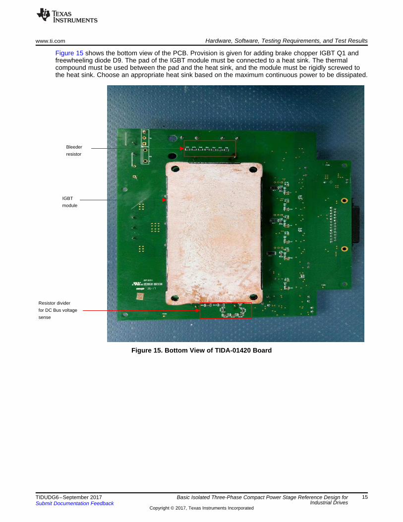
Figure 15 shows the bottom view of the PCB. Provision is given for adding brake chopper IGBT Q1 andfreewheeling diode D9. The pad of the IGBT module must be connected to a heat sink. The thermalcompound must be used between the pad and the heat sink, and the module must be rigidly screwed tothe heat sink. Choose an appropriate heat sink based on the maximum continuous power to be dissipated.
Figure 15. Bottom View of TIDA-01420 Board
Interfaced together with ribbon cable TMDSCNCD28379D Delfino Control Card
Adapter PCB
Hardware, Software, Testing Requirements, and Test Results www.ti.com
16 TIDUDG6–September 2017Submit Documentation Feedback
Copyright © 2017, Texas Instruments Incorporated
Basic Isolated Three-Phase Compact Power Stage Reference Design forIndustrial Drives
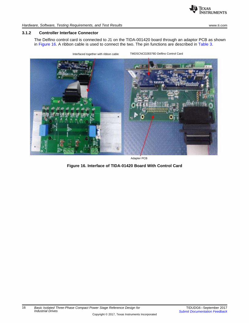
3.1.2 Controller Interface ConnectorThe Delfino control card is connected to J1 on the TIDA-001420 board through an adaptor PCB as shownin Figure 16. A ribbon cable is used to connect the two. The pin functions are described in Table 3.
Figure 16. Interface of TIDA-01420 Board With Control Card
www.ti.com Hardware, Software, Testing Requirements, and Test Results
17TIDUDG6–September 2017Submit Documentation Feedback
Copyright © 2017, Texas Instruments Incorporated
Basic Isolated Three-Phase Compact Power Stage Reference Design forIndustrial Drives
Table 3. Connector Pin Description
PIN NUMBER PIN NAME I/O DESCRIPTION
1 5V0 Power 5-V input to the primary side of the powerstage
2 PWM_UB+ 3.3-V input Phase U low-side gate driver PWM input3 PWM_UT+ 3.3-V input Phase U high-side gate driver PWM input4 PWM_VB+ 3.3-V input Phase V low-side gate driver PWM input5 PWM_VT+ 3.3-V input Phase V high-side gate driver PWM input6 PWM_WB+ 3.3-V input Phase W low-side gate driver PWM input7 PWM_WT+ 3.3-V input Phase W high-side gate driver PWM input8 PWM_BRAKE+ 3.3-V input PWM input to brake IGBT gate driver9 NC NA N/A
10 MDATA_U 3.3-V output U phase current measurement data fromΔΣ modulator
11 NC NA N/A
12 MDATA_W 3.3-V output W phase current measurement data fromΔΣ modulator
13 5V0 Power 5-V input to the primary side of the powerstage
14 GND Power Primary-side ground15 GND Power Primary-side ground16 GND Power Primary-side ground17 GND Power Primary-side ground18 GND Power Primary-side ground19 GND Power Primary-side ground20 GND Power Primary-side ground21 NC NA N/A
22 CLK 3.3-V input Clock input to TIDA-01420 from thecontrol card
23 MDATA_VDC 3.3-V output DC bus voltage measurement data fromΔΣ modulator
24 MDATA_TMP 3.3-V output Temperature measurement data from ΔΣmodulator
25 GND Power Primary-side ground
3.2 Testing and Results
3.2.1 Test SetupThe focus of the tests is to evaluate the functionality and performance of the basic isolated gate driversUCC5350MCD and UCC5390ECD. The IGBT used for testing UCC5350MCD is CM100TX-24S whereasthe IGBT used for testing UCC5390ECD is 6MI180VB-120-50.

PWM1 A/B
PWM2 A/B
PWM3 A/B
Mfunc_C1
Mfunc_C3
Mfunc_C2
Ta
Tc
Tb
Ualpha
Ubeta
PWMDAC
MACROMFuncC1
MFuncC2
PWMxA
PWMxB
Low
Pass
Filter
Cct
DATALOG
Dlog1
Dlog2
Dlog3
Dlog4
Scope
Graph
Window
Alpha
Beta
Ds
Angle
Qs
VdTesting
VqTesting
PM
Motor
3-Phase
Inverter
PWM
MACRO
PWM
HW
ADCIn1 (Iu)
ADCIn2 (Iw)
ADCIn3 (Temp)
IPARK
MACRO
CLARKE
MACROAdcResult0
AdcResult1
As
Bs
Alpha
Beta
PARK
MACRO
Alpha
Beta
ADCIn4 (Vdc)AdcResult3
SVGEN
MACRO
Vabc
Valpha
Vbeta
TargetValue
RC
MACROSetPointValue
RG
MACROFreq
SpeedRef
OutSine/Cos
Ta
Tc
Tb
DcBusVolt
SDFM
MACRO
PHASE
VOLT
MACRO
HW
SDFM
Angle Variable
Isw = 1
Isw = 0
Switched manually in CCSwatch window
Copyright © 2017, Texas Instruments Incorporated
Hardware, Software, Testing Requirements, and Test Results www.ti.com
18 TIDUDG6–September 2017Submit Documentation Feedback
Copyright © 2017, Texas Instruments Incorporated
Basic Isolated Three-Phase Compact Power Stage Reference Design forIndustrial Drives
3.2.2 SoftwareThis reference design is tested using software modified from the application report Sensorless Field Oriented Control of 3-Phase PermanentMagnet Synchronous Motors Using TMS320F2833x. The incremental build level 2 shown in Figure 17 is modified. A switch is added to connecteither the OUT signal coming from the RG MACRO or the angle variable to the sine cos block. Connecting OUT enables the design to pumpsinusoidal current into the motor. Connecting the angle variable, which is made zero, enables driving DC current into the motor
Figure 17. PWM Control and Current Sense Software
ControllerIGBT gate
driverPWM
Point 1
Rg
Point 2
www.ti.com Hardware, Software, Testing Requirements, and Test Results
19TIDUDG6–September 2017Submit Documentation Feedback
Copyright © 2017, Texas Instruments Incorporated
Basic Isolated Three-Phase Compact Power Stage Reference Design forIndustrial Drives
3.2.3 Test Results for UCC5350MCD
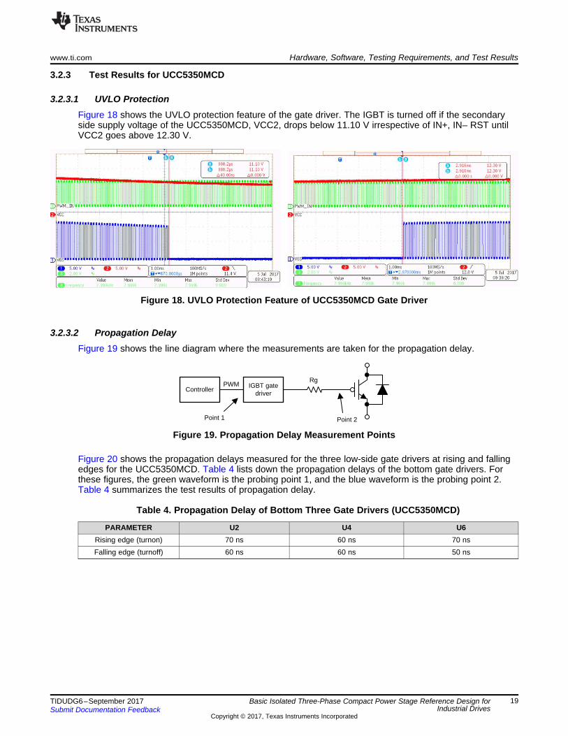
3.2.3.1 UVLO ProtectionFigure 18 shows the UVLO protection feature of the gate driver. The IGBT is turned off if the secondaryside supply voltage of the UCC5350MCD, VCC2, drops below 11.10 V irrespective of IN+, IN– RST untilVCC2 goes above 12.30 V.
Figure 18. UVLO Protection Feature of UCC5350MCD Gate Driver
3.2.3.2 Propagation DelayFigure 19 shows the line diagram where the measurements are taken for the propagation delay.
Figure 19. Propagation Delay Measurement Points
Figure 20 shows the propagation delays measured for the three low-side gate drivers at rising and fallingedges for the UCC5350MCD. Table 4 lists down the propagation delays of the bottom gate drivers. Forthese figures, the green waveform is the probing point 1, and the blue waveform is the probing point 2.Table 4 summarizes the test results of propagation delay.
Table 4. Propagation Delay of Bottom Three Gate Drivers (UCC5350MCD)
PARAMETER U2 U4 U6Rising edge (turnon) 70 ns 60 ns 70 nsFalling edge (turnoff) 60 ns 60 ns 50 ns

Voltagedrop across external resistor during IGBT turnoff 11.3 VSink Current 0.941A
Value of external resistor 12= = =
W
Voltagedrop across external resistor during IGBT turnon 7.1VSource Current 0.591A
Value of external resistor 12= = =
W
Gate VoltageSink CurrentGate Voltage
Source Current
Hardware, Software, Testing Requirements, and Test Results www.ti.com
20 TIDUDG6–September 2017Submit Documentation Feedback
Copyright © 2017, Texas Instruments Incorporated
Basic Isolated Three-Phase Compact Power Stage Reference Design forIndustrial Drives
Note that the maximum skew between the propagation delay is 10 ns. Low propagation delay allows thedesign to achieve high switching speeds.
Figure 20. Propagation Delay of Bottom Gate Drivers (UCC5350MCD)
3.2.3.3 Source/Sink CurrentsThe source and sink current waveforms have been captured for the bottom IGBTs by measuring thevoltage drop across the gate resistors. Figure 21 shows the source and sink currents provided by theUCC5350MCD for charging the gate of the IGBT at DC bus voltage of 565 V. The external gate resistorused in this case is 12 Ω, which is in accordance to the recommendation specified in the IGBT datasheet.
Figure 21. Source and Sink Currents With IGBT Module at DC Bus Voltage of 565 V With UCC5350MCD
(2)
(3)

DS,offVt3 _ off CRSS
Ig3= ´
DRV MillerV VIg3 _ off
R _ Total
-
=
MillerVt1 t2 _ on CISS
Ig1 Ig2+ = ´
+
DRV MillerV 0.5 VIg1 Ig2 _ on
R _ Total
- ´
+ =
Voltagedrop across external resistor during IGBT turnoff 8.2 VSink Current 5.47 A
Value of external resistor 1.5= = =
W
Voltagedrop across external resistor during IGBT turnon 7 VSource Current 4.67 A
Value of external resistor 1.5= = =
W
Capacitor ChargingSource Current
Capacitor DischargingSink Current
www.ti.com Hardware, Software, Testing Requirements, and Test Results
21TIDUDG6–September 2017Submit Documentation Feedback
Copyright © 2017, Texas Instruments Incorporated
Basic Isolated Three-Phase Compact Power Stage Reference Design forIndustrial Drives
However, the source and sink capabilities of the device is greater than these specified values. TheUCC5350MCD can easily drive an IGBT of a high-input capacitance value. This has been verified byreplacing the IGBT modules with an external capacitor of 56 nF and measuring the source and sinkcurrents as shown in Figure 22. The value of external gate resistor used for making these measurementsis 1 Ω with the UCC5350MCD. Equation 4. Equation 5 shows the sourcing and sinking capability of gatedrivers when the external capacitor is used.
Figure 22. Source and Sink Currents of UCC5350MCD With 56-nF Capacitor
(4)
(5)
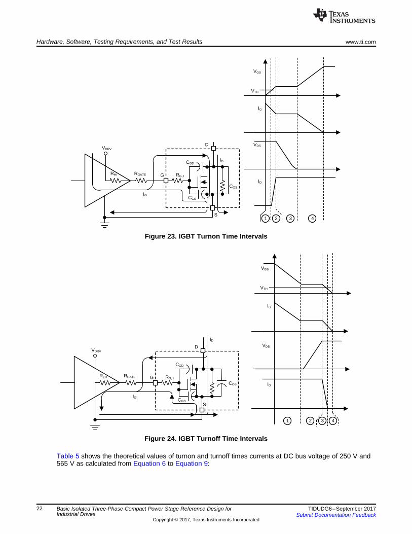
3.2.3.4 Turn on and Turn off of IGBTFigure 23 and Figure 24 show the IGBT turnon and turnoff time intervals. A crude estimate of the IGBTcharging and discharging times can be calculated using simplified linear approximations of the gate drivecurrent, drain current, and drain voltage waveforms during periods 2 and 3 of the switching transitions.
Equation 6 and Equation 7 show the charging times:
(6)
(7)
Equation 8 and Equation 9 show the discharging times:
(8)
(9)
1 2 3 4
ID
VDS
IG
VTH
VGS
ID
D
S
COS
CGS
CGD
RG, IG
IG
RGATERLO
VDRV
1 2 3 4
ID
VDS
IG
VTH
VGS
ID
D
S
COS
CGS
CGD
RG, IG
IG
RGATERHI
VDRV
Hardware, Software, Testing Requirements, and Test Results www.ti.com
22 TIDUDG6–September 2017Submit Documentation Feedback
Copyright © 2017, Texas Instruments Incorporated
Basic Isolated Three-Phase Compact Power Stage Reference Design forIndustrial Drives
Figure 23. IGBT Turnon Time Intervals
Figure 24. IGBT Turnoff Time Intervals
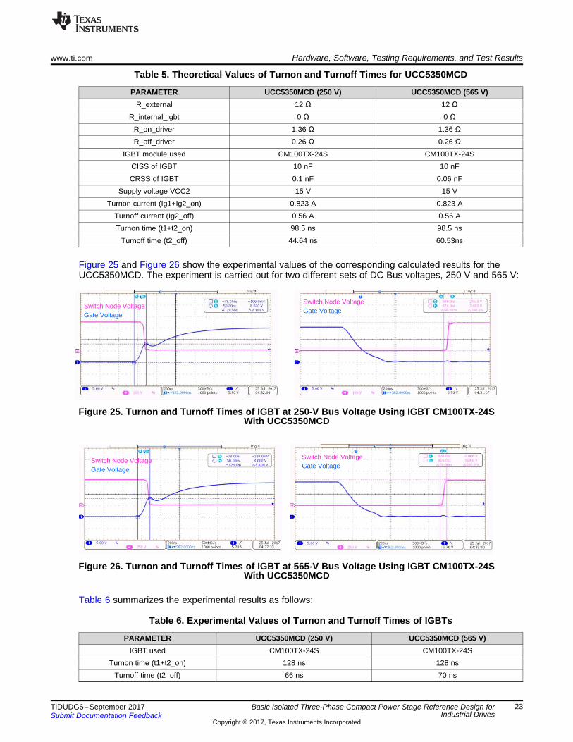
Table 5 shows the theoretical values of turnon and turnoff times currents at DC bus voltage of 250 V and565 V as calculated from Equation 6 to Equation 9:
Switch Node VoltageGate Voltage
Switch Node VoltageGate Voltage
Switch Node VoltageGate Voltage
Switch Node VoltageGate Voltage
www.ti.com Hardware, Software, Testing Requirements, and Test Results
23TIDUDG6–September 2017Submit Documentation Feedback
Copyright © 2017, Texas Instruments Incorporated
Basic Isolated Three-Phase Compact Power Stage Reference Design forIndustrial Drives
Table 5. Theoretical Values of Turnon and Turnoff Times for UCC5350MCD
PARAMETER UCC5350MCD (250 V) UCC5350MCD (565 V)R_external 12 Ω 12 Ω
R_internal_igbt 0 Ω 0 ΩR_on_driver 1.36 Ω 1.36 ΩR_off_driver 0.26 Ω 0.26 Ω
IGBT module used CM100TX-24S CM100TX-24SCISS of IGBT 10 nF 10 nFCRSS of IGBT 0.1 nF 0.06 nF
Supply voltage VCC2 15 V 15 VTurnon current (Ig1+Ig2_on) 0.823 A 0.823 A
Turnoff current (Ig2_off) 0.56 A 0.56 ATurnon time (t1+t2_on) 98.5 ns 98.5 ns
Turnoff time (t2_off) 44.64 ns 60.53ns
Figure 25 and Figure 26 show the experimental values of the corresponding calculated results for theUCC5350MCD. The experiment is carried out for two different sets of DC Bus voltages, 250 V and 565 V:
Figure 25. Turnon and Turnoff Times of IGBT at 250-V Bus Voltage Using IGBT CM100TX-24SWith UCC5350MCD
Figure 26. Turnon and Turnoff Times of IGBT at 565-V Bus Voltage Using IGBT CM100TX-24SWith UCC5350MCD
Table 6 summarizes the experimental results as follows:
Table 6. Experimental Values of Turnon and Turnoff Times of IGBTs
PARAMETER UCC5350MCD (250 V) UCC5350MCD (565 V)IGBT used CM100TX-24S CM100TX-24S
Turnon time (t1+t2_on) 128 ns 128 nsTurnoff time (t2_off) 66 ns 70 ns
Hardware, Software, Testing Requirements, and Test Results www.ti.com
24 TIDUDG6–September 2017Submit Documentation Feedback
Copyright © 2017, Texas Instruments Incorporated
Basic Isolated Three-Phase Compact Power Stage Reference Design forIndustrial Drives
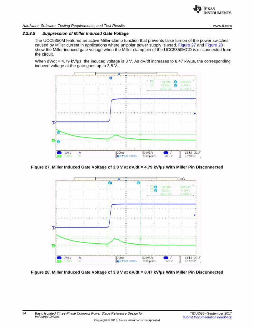
3.2.3.5 Suppression of Miller Induced Gate VoltageThe UCC5350M features an active Miller-clamp function that prevents false turnon of the power switchescaused by Miller current in applications where unipolar power supply is used. Figure 27 and Figure 28show the Miller induced gate voltage when the Miller clamp pin of the UCC5350MCD is disconnected fromthe circuit.
When dV/dt = 4.79 kV/µs, the induced voltage is 3 V. As dV/dt increases to 8.47 kV/µs, the correspondinginduced voltage at the gate goes up to 3.8 V.
Figure 27. Miller Induced Gate Voltage of 3.0 V at dV/dt = 4.79 kV/µs With Miller Pin Disconnected
Figure 28. Miller Induced Gate Voltage of 3.8 V at dV/dt = 8.47 kV/µs With Miller Pin Disconnected

www.ti.com Hardware, Software, Testing Requirements, and Test Results
25TIDUDG6–September 2017Submit Documentation Feedback
Copyright © 2017, Texas Instruments Incorporated
Basic Isolated Three-Phase Compact Power Stage Reference Design forIndustrial Drives
Figure 29 and Figure 30 show the same set of test results when the Miller clamp pin is reconnected to thecircuit. The induced voltage is suppressed as the Miller current sinks through the low impedance pathbetween the power switch gate terminal and ground, VEE2.
Figure 29. No Voltage Induced at dV/dt = 4.79 kV/µs With Miller Pin Connected
Figure 30. No Voltage Induced at dV/dt = 8.47 kV/µs With Miller Pin Connected
Table 7 summarizes the test results as follows:
Table 7. Summary of Miller Induced Gate Voltages at Different dV/dt
MILLER PIN STATUS dV/dt MILLER INDUCTED (kV/µs) GATE VOLTAGE (V)Disconnected 4.8 3.0
Connected 4.8 0Disconnected 8.5 3.8
Connected 8.5 0

VCC2 Supply VoltageSwitch Node Voltage
VCC2 Supply VoltageSwitch Node Voltage
VCC2 Supply VoltageSwitch Node Voltage
Supply Voltage RippleSwitch Node Voltage
Supply Voltage RippleSwitch Node Voltage
Supply Voltage RippleSwitch Node Voltage
Hardware, Software, Testing Requirements, and Test Results www.ti.com
26 TIDUDG6–September 2017Submit Documentation Feedback
Copyright © 2017, Texas Instruments Incorporated
Basic Isolated Three-Phase Compact Power Stage Reference Design forIndustrial Drives
3.2.3.6 Power Supply Rail for High-Side Gate Drivers (Bootstrap Supply)Figure 31 shows the ripple on the bootstrap voltage and the switch node voltage. The bus voltage appliedwhile taking these measurements is 50 V. The bus voltage had to be limited to 50 V during the experimentdue to the constraint put by the common-mode rejection ratio of the oscilloscope. The duty cycle of thePWM signal is varied to see the variations in the power supply ripple voltage. Table 8 summarizes theresults.
Table 8. Summary of Variation of Bootstrap Ripple Voltage With Duty Cycle
DUTY CYCLE RIPPLE VOLTAGE on POWER SUPPLY (mV)90% 44050% 84010% 1320
Figure 31. Variation of Bootstrap Supply Ripple With Change in Duty Cycle
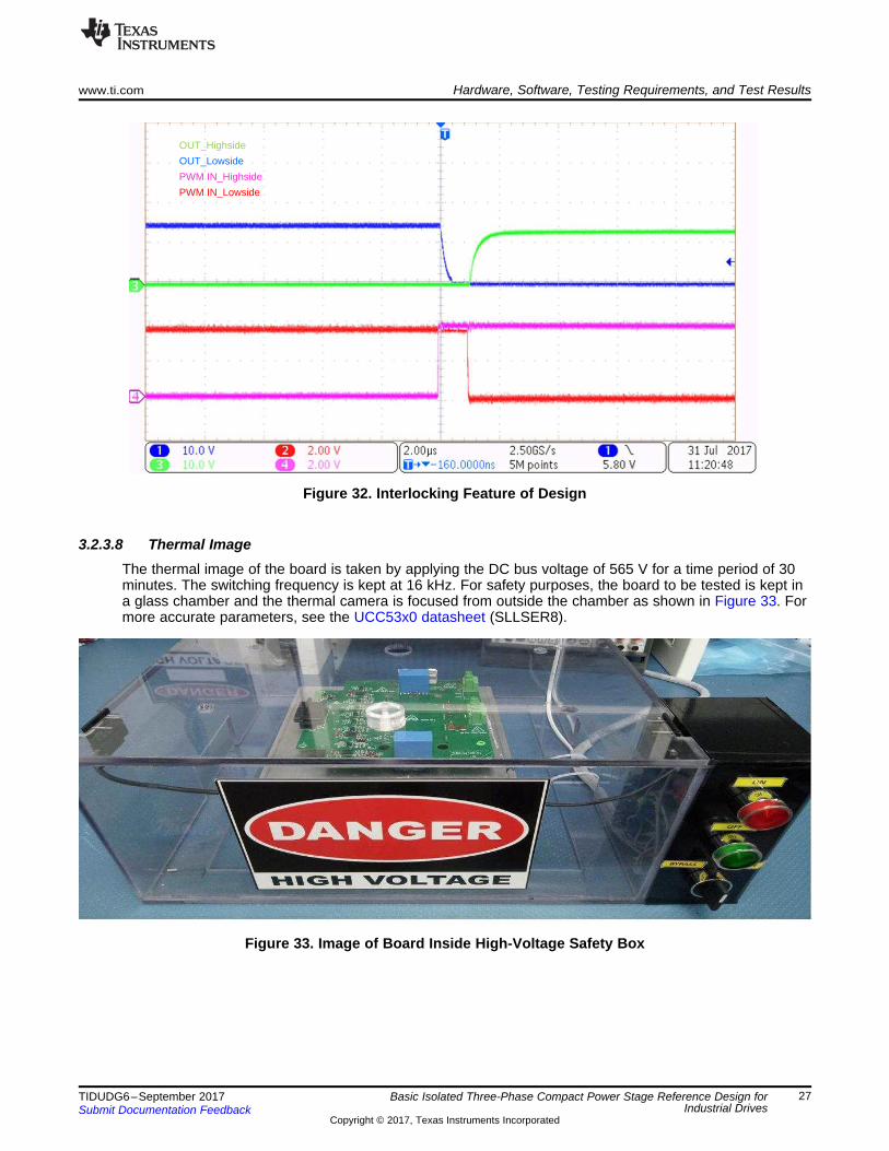
3.2.3.7 Interlocking FunctioningThis experiment is done by applying a negative deadband (setting both high-side and low-side PWMsignals high for a certain time) at the inputs of the gate drivers. Figure 32 shows that because ofinterlocking, the negative dead time at the input is converted into positive dead band at the output of thegate driver. Thus, this protection feature avoids the possibility of shoot-through.
OUT_Highside
OUT_Lowside
PWM IN_Highside
PWM IN_Lowside
www.ti.com Hardware, Software, Testing Requirements, and Test Results
27TIDUDG6–September 2017Submit Documentation Feedback
Copyright © 2017, Texas Instruments Incorporated
Basic Isolated Three-Phase Compact Power Stage Reference Design forIndustrial Drives
Figure 32. Interlocking Feature of Design
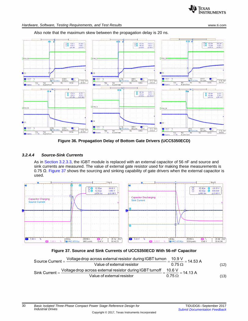
3.2.3.8 Thermal ImageThe thermal image of the board is taken by applying the DC bus voltage of 565 V for a time period of 30minutes. The switching frequency is kept at 16 kHz. For safety purposes, the board to be tested is kept ina glass chamber and the thermal camera is focused from outside the chamber as shown in Figure 33. Formore accurate parameters, see the UCC53x0 datasheet (SLLSER8).
Figure 33. Image of Board Inside High-Voltage Safety Box

Hardware, Software, Testing Requirements, and Test Results www.ti.com
28 TIDUDG6–September 2017Submit Documentation Feedback
Copyright © 2017, Texas Instruments Incorporated
Basic Isolated Three-Phase Compact Power Stage Reference Design forIndustrial Drives
Figure 34 shows the thermal image of the boards UCC5350MCD respectively and the correspondingminimum, maximum, and average temperatures. The ambient temperature while making thesemeasurements is 25°C.
Figure 34. Thermal Image of Board With Gate Driver UCC5350MCD
3.2.4 Test Results for UCC5390ECD
3.2.4.1 UVLO ProtectionThe UCC5390ECD has an external pin for UVLO measurement, which is referenced to ground rather thanVEE2. As shown in Figure 35, IGBT is turned off if the secondary side supply voltage of theUCC5390ECD, VCC2, drops below 11.09 V irrespective of IN+, IN– until VCC2 goes above 12 V.
Figure 35. UVLO Protection Feature of UCC5390ECD Gate Driver

GSW SWP Qg Vg f= ´ ´
GDQP VCC1 ICC1 VCC2 ICC2 VCC2 ICC2= ´ + ´ » ´
www.ti.com Hardware, Software, Testing Requirements, and Test Results
29TIDUDG6–September 2017Submit Documentation Feedback
Copyright © 2017, Texas Instruments Incorporated
Basic Isolated Three-Phase Compact Power Stage Reference Design forIndustrial Drives
3.2.4.2 Power Consumption by Gate DriversIn this experiment, the UCC5390ECD is used to drive the IGBT module, 6MI180VB-120-50. The staticpower loss, PGDQ includes quiescent power loss on the driver as well as driver self-power consumptionwhen operating with a certain switching frequency. The power supplied by the gate driver can becalculated by measuring the average current consumed by it as shown in Equation 10.
(10)
Table 9 shows the power supplied to the gate driver at 8- and 16-kHz switching frequencies:
Table 9. Power Supplied to Bottom Gate Drivers
FREQSWITCHING SUPPLY CURRENT (ICC2)
SUPPLYVOLTAGE
(VCC2)POWER SUPPLIED, PGDQ
(3 DRIVERS)POWER SUPPLIED, PGDQ
(PER GATE DRIVER)
8 kHz 0.075 A 24 V 1.8 W 0.6 W16 kHz 0.127 A 24 V 3.048 W 1.016 W
The power lost to drive the gate of the IGBT, that is the switching operation loss, can be calculated asfollows:
(11)
To compare the switching operation loss with the quiescent power loss, PGSW is calculated for two differentfrequencies- (8 kHz and 16 kHz) and is summarized in Table 10:
Table 10. Power Lost to Gate During Switching
FREQ SWITCHING (fSW) Q_g V_g PGSW
8 kHz 2000 nC 24 V 0.348 W16 kHz 2000 nc 24 V 0.768 W
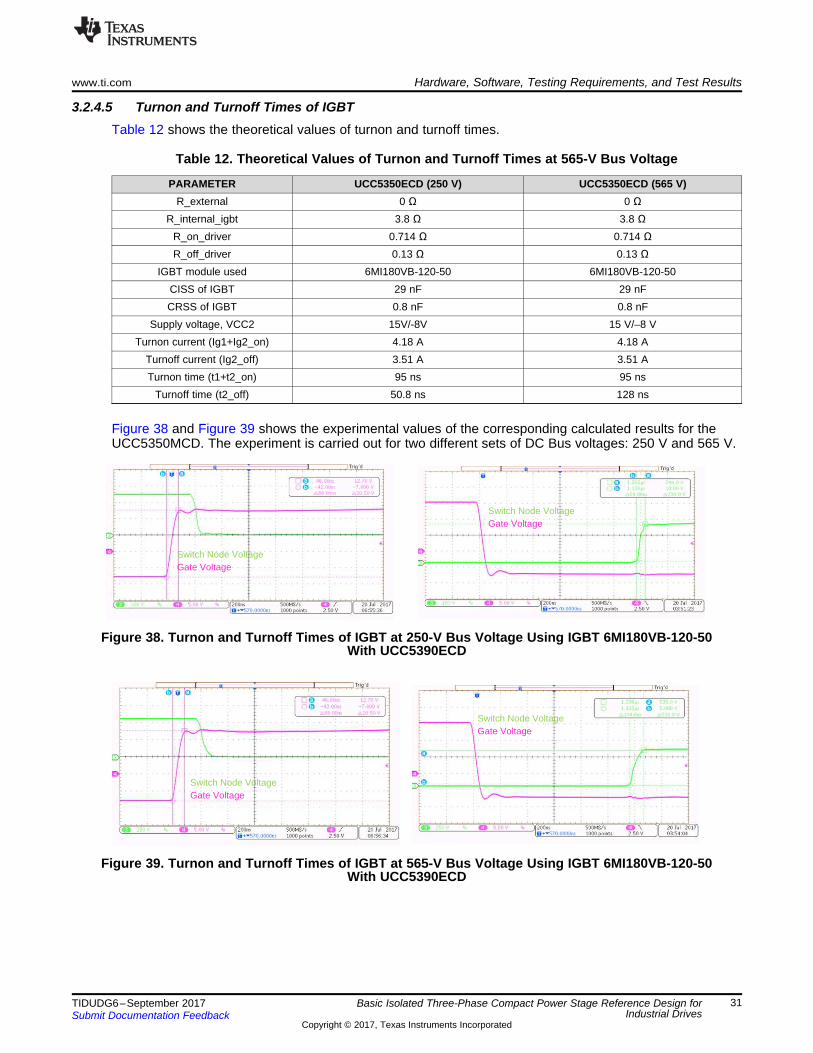
3.2.4.3 Propagation DelayFigure 36 shows the propagation delays measured for the three low-side gate drivers at rising and fallingedges for the UCC5390ECD.Table 11 lists the propagation delays of the bottom gate drivers.
Table 11. Propagation Delay of Bottom Three Gate Drivers (UCC5390ECD)
PARAMETER U2 U4 U6Rising edge (turnon) 80 ns 80 ns 100 nsFalling edge (turnoff) 72 ns 90 ns 80 ns
Voltagedrop across external resistor during IGBT turnoff 10.6 VSink Current 14.13 A
Value of external resistor 0.75= = =
W
Voltagedrop across external resistor during IGBT turnon 10.9 VSource Current 14.53 A
Value of external resistor 0.75= = =
W
Capacitor ChargingSource Current
Capacitor DischargingSink Current
Hardware, Software, Testing Requirements, and Test Results www.ti.com
30 TIDUDG6–September 2017Submit Documentation Feedback
Copyright © 2017, Texas Instruments Incorporated
Basic Isolated Three-Phase Compact Power Stage Reference Design forIndustrial Drives
Also note that the maximum skew between the propagation delay is 20 ns.
Figure 36. Propagation Delay of Bottom Gate Drivers (UCC5350ECD)
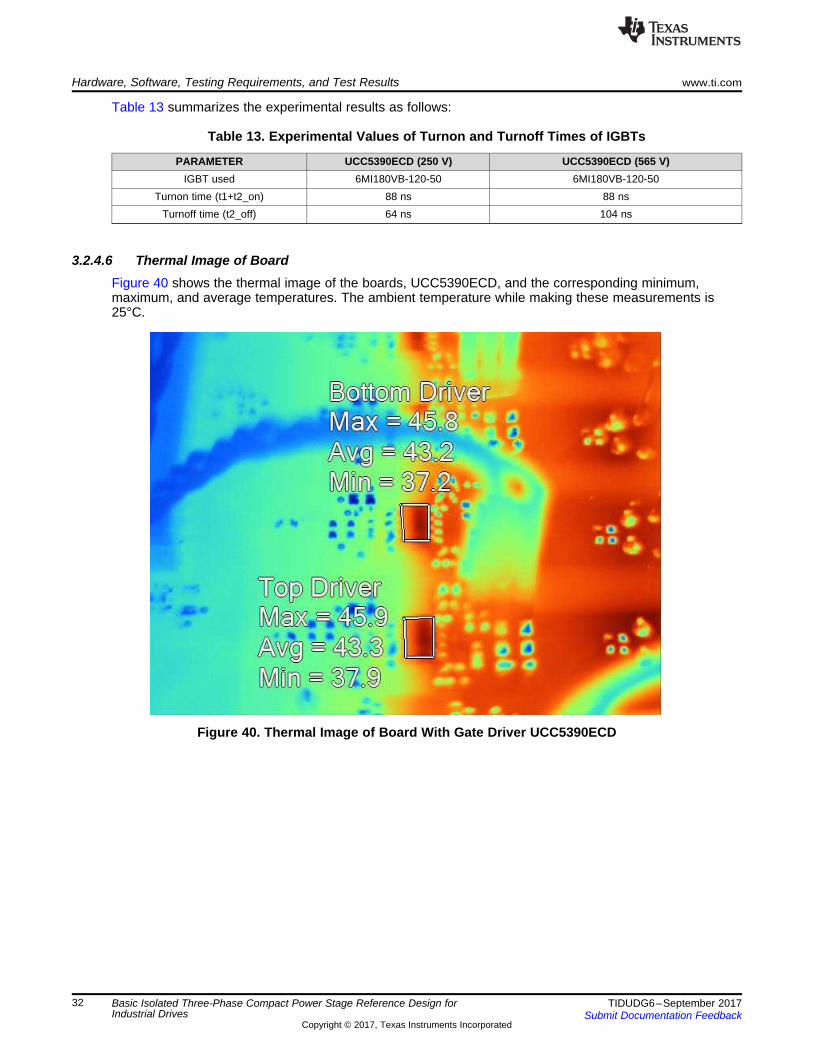
3.2.4.4 Source-Sink CurrentsAs in Section 3.2.3.3, the IGBT module is replaced with an external capacitor of 56 nF and source andsink currents are measured. The value of external gate resistor used for making these measurements is0.75 Ω. Figure 37 shows the sourcing and sinking capability of gate drivers when the external capacitor isused.
Figure 37. Source and Sink Currents of UCC5350ECD With 56-nF Capacitor
(12)
(13)
Switch Node VoltageGate Voltage
Switch Node VoltageGate Voltage
Switch Node VoltageGate Voltage
Switch Node VoltageGate Voltage
www.ti.com Hardware, Software, Testing Requirements, and Test Results
31TIDUDG6–September 2017Submit Documentation Feedback
Copyright © 2017, Texas Instruments Incorporated
Basic Isolated Three-Phase Compact Power Stage Reference Design forIndustrial Drives
3.2.4.5 Turnon and Turnoff Times of IGBTTable 12 shows the theoretical values of turnon and turnoff times.
Table 12. Theoretical Values of Turnon and Turnoff Times at 565-V Bus Voltage
PARAMETER UCC5350ECD (250 V) UCC5350ECD (565 V)R_external 0 Ω 0 Ω
R_internal_igbt 3.8 Ω 3.8 ΩR_on_driver 0.714 Ω 0.714 ΩR_off_driver 0.13 Ω 0.13 Ω
IGBT module used 6MI180VB-120-50 6MI180VB-120-50CISS of IGBT 29 nF 29 nFCRSS of IGBT 0.8 nF 0.8 nF
Supply voltage, VCC2 15V/-8V 15 V/–8 VTurnon current (Ig1+Ig2_on) 4.18 A 4.18 A
Turnoff current (Ig2_off) 3.51 A 3.51 ATurnon time (t1+t2_on) 95 ns 95 ns
Turnoff time (t2_off) 50.8 ns 128 ns
Figure 38 and Figure 39 shows the experimental values of the corresponding calculated results for theUCC5350MCD. The experiment is carried out for two different sets of DC Bus voltages: 250 V and 565 V.
Figure 38. Turnon and Turnoff Times of IGBT at 250-V Bus Voltage Using IGBT 6MI180VB-120-50With UCC5390ECD
Figure 39. Turnon and Turnoff Times of IGBT at 565-V Bus Voltage Using IGBT 6MI180VB-120-50With UCC5390ECD
Hardware, Software, Testing Requirements, and Test Results www.ti.com
32 TIDUDG6–September 2017Submit Documentation Feedback
Copyright © 2017, Texas Instruments Incorporated
Basic Isolated Three-Phase Compact Power Stage Reference Design forIndustrial Drives
Table 13 summarizes the experimental results as follows:
Table 13. Experimental Values of Turnon and Turnoff Times of IGBTs
PARAMETER UCC5390ECD (250 V) UCC5390ECD (565 V)IGBT used 6MI180VB-120-50 6MI180VB-120-50
Turnon time (t1+t2_on) 88 ns 88 nsTurnoff time (t2_off) 64 ns 104 ns
3.2.4.6 Thermal Image of BoardFigure 40 shows the thermal image of the boards, UCC5390ECD, and the corresponding minimum,maximum, and average temperatures. The ambient temperature while making these measurements is25°C.
Figure 40. Thermal Image of Board With Gate Driver UCC5390ECD
Basic isolation
spacing of 4 mm
Single point
contact
Power ground
DC-
Low-side gate
driver ground
www.ti.com Design Files
33TIDUDG6–September 2017Submit Documentation Feedback
Copyright © 2017, Texas Instruments Incorporated
Basic Isolated Three-Phase Compact Power Stage Reference Design forIndustrial Drives
4 Design Files
4.1 SchematicsTo download the schematics, see the design files at TIDA-01420 .
4.2 Bill of MaterialsTo download the bill of materials (BOM), see the design files at TIDA-01420.
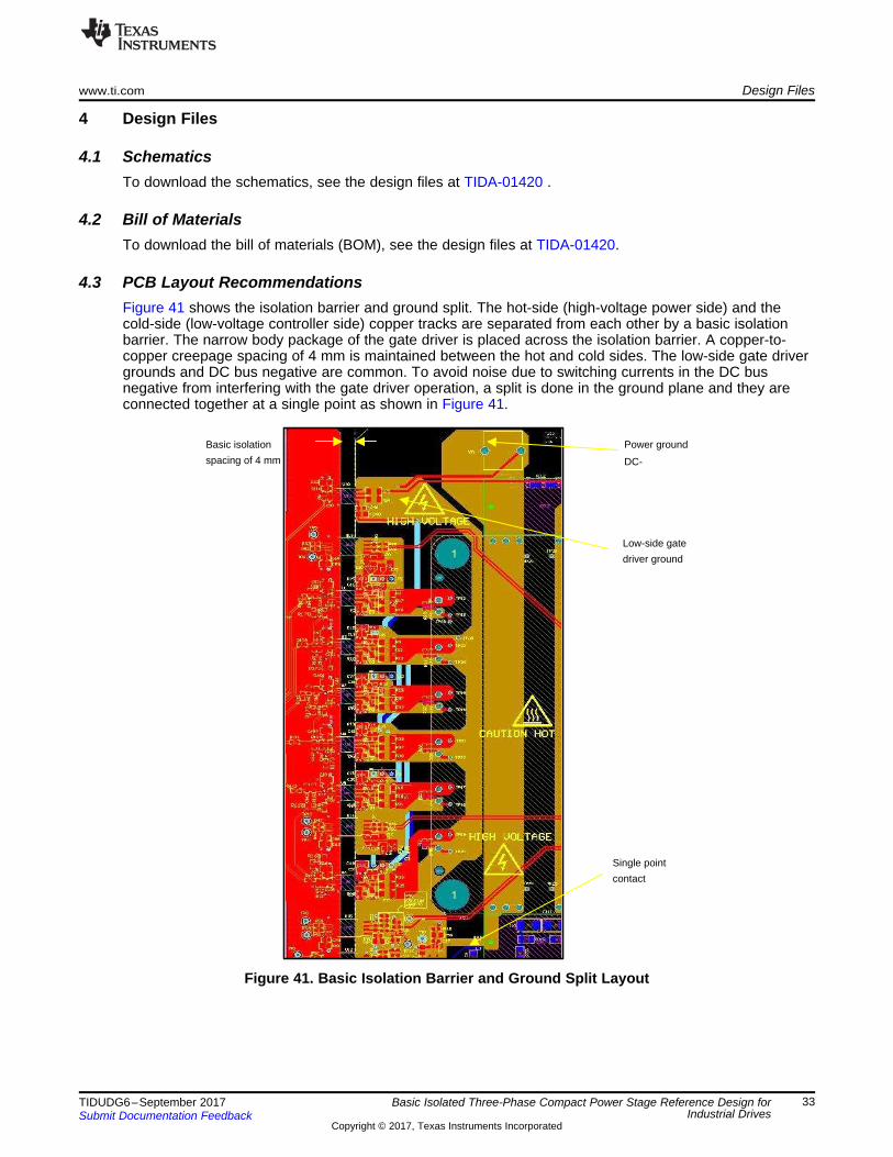
4.3 PCB Layout RecommendationsFigure 41 shows the isolation barrier and ground split. The hot-side (high-voltage power side) and thecold-side (low-voltage controller side) copper tracks are separated from each other by a basic isolationbarrier. The narrow body package of the gate driver is placed across the isolation barrier. A copper-to-copper creepage spacing of 4 mm is maintained between the hot and cold sides. The low-side gate drivergrounds and DC bus negative are common. To avoid noise due to switching currents in the DC busnegative from interfering with the gate driver operation, a split is done in the ground plane and they areconnected together at a single point as shown in Figure 41.
Figure 41. Basic Isolation Barrier and Ground Split Layout

Differential routing
Kelvin connection
Design Files www.ti.com
34 TIDUDG6–September 2017Submit Documentation Feedback
Copyright © 2017, Texas Instruments Incorporated
Basic Isolated Three-Phase Compact Power Stage Reference Design forIndustrial Drives
The shunt resistance of 4 mΩ is in the same range as that of the stray parasitic trace resistances. Foraccurate shunt-based current sensing, it is important to sense the exact voltage across the shunt resistoronly and avoid measuring the drop across the trace and contact parasitic resistance. This is done byimplementing a Kelvin connection as shown inFigure 42. Differential routing is done from the shuntresistor to the ΔΣ modulator. Any noise is common to both the traces and gets cancelled off in thedifferential input stage of the modulator.
Figure 42. Shunt Resistor Connection to ΔΣ Modulator Layout
As shown in Figure 43, the primary- and secondary-side noise-decoupling capacitors must be connectedclose to the device between the VCC1 and GND1 pins and between the VCC2 and VEE2 pins to bypassnoise and to support high peak currents when turning on the IGBT. It is essential to limit the high peakcurrents that charge and discharge the IGBT gates to a minimal physical area. This limitation decreasesthe loop inductance and minimizes noise on the gate terminals of the IGBTs. The gate driver must beplaced as close as possible to the IGBTs. To ensure isolation performance between the primary andsecondary side, avoid placing any PCB traces or copper below the driver device.

www.ti.com Design Files
35TIDUDG6–September 2017Submit Documentation Feedback
Copyright © 2017, Texas Instruments Incorporated
Basic Isolated Three-Phase Compact Power Stage Reference Design forIndustrial Drives
Figure 43. Low-Side Gate Driver Layout
Figure 44 shows the DC bus voltage sense circuit. The high-impedance resistor divider network isconnected across the pins of the high-voltage DC-link film capacitor C111. The attenuated voltage issensed by ΔΣ modulator U12. It is important to sense the voltage across the film capacitor for low-noisemeasurement.
Figure 44. Connection of DC Bus Voltage Sensing
4.3.1 Layout PrintsTo download the layer plots, see the design files at TIDA-01420.
4.4 Altium ProjectTo download the Altium project files, see the design files at TIDA-01420.

Design Files www.ti.com
36 TIDUDG6–September 2017Submit Documentation Feedback
Copyright © 2017, Texas Instruments Incorporated
Basic Isolated Three-Phase Compact Power Stage Reference Design forIndustrial Drives
4.5 Gerber FilesTo download the Gerber files, see the design files at TIDA-01420.
4.6 Assembly DrawingsTo download the assembly drawings, see the design files at TIDA-01420.
5 Related Documentation1. Texas Instruments, Reinforced Isolated Phase Current Sense Reference Design With Small Delta-
Sigma Modulators, TIDA-00914 Design Guide (TIDUD07)2. Texas Instruments, Isolated Current Shunt and Voltage Measurement Kit, TIDA-00171 Design Guide
(TIDU499)3. Texas Instruments, Isolated Current Shunt and Voltage Measurement for Motor Drives Using AM437x,
TIDA-00209 Design Guide (TIDU755)4. Texas Instruments, Sensorless Field Oriented Control of 3-Phase Permanent Magnet Synchronous
Motors Using TMS320F2833x, Application Report (SPRABQ4)5. Texas Instruments, Wide-Input Isolated IGBT Gate-Drive Fly-Buck™ Power Supply for Three-Phase
Inverters, TIDA-00199 Design Guide (TIDU670)6. Texas Instruments, Reference Design for Reinforced Isolation Three-Phase Inverter With Current,
Voltage, and Temp Protection, TIDA-00366 Design Guide (TIDUBX1)
5.1 TrademarksDelfino is a trademark of Texas Instruments.All other trademarks are the property of their respective owners.
6 TerminologyIGBT— Insulated gate bipolar transistor
VFD— Variable frequency drive
PWM— Pulse width modulation
UVLO— Undervoltage lockout
DNP— Do not populate
7 About the AuthorsAISHWARYA BHATNAGAR is a systems engineer at Texas Instruments, where she is responsible fordeveloping reference design solutions for the Motor Drive segment within Industrial Systems. Aishwaryaearned her bachelor of technology in electronics and communication engineering from MNNIT, Allahabad.
MARTIN STAEBLER is a system architect in the Industrial Systems-Motor Drive team at TexasInstruments, responsible for specifying reference designs for industrial drives.
7.1 RecognitionThe authors would like to recognize the excellent contributions from PAWAN NAYAK and NELSONALEXANDER during the design, test, and documentation phases of the TIDA-01420 reference design.

IMPORTANT NOTICE FOR TI DESIGN INFORMATION AND RESOURCES
Texas Instruments Incorporated (‘TI”) technical, application or other design advice, services or information, including, but not limited to,reference designs and materials relating to evaluation modules, (collectively, “TI Resources”) are intended to assist designers who aredeveloping applications that incorporate TI products; by downloading, accessing or using any particular TI Resource in any way, you(individually or, if you are acting on behalf of a company, your company) agree to use it solely for this purpose and subject to the terms ofthis Notice.TI’s provision of TI Resources does not expand or otherwise alter TI’s applicable published warranties or warranty disclaimers for TIproducts, and no additional obligations or liabilities arise from TI providing such TI Resources. TI reserves the right to make corrections,enhancements, improvements and other changes to its TI Resources.You understand and agree that you remain responsible for using your independent analysis, evaluation and judgment in designing yourapplications and that you have full and exclusive responsibility to assure the safety of your applications and compliance of your applications(and of all TI products used in or for your applications) with all applicable regulations, laws and other applicable requirements. Yourepresent that, with respect to your applications, you have all the necessary expertise to create and implement safeguards that (1)anticipate dangerous consequences of failures, (2) monitor failures and their consequences, and (3) lessen the likelihood of failures thatmight cause harm and take appropriate actions. You agree that prior to using or distributing any applications that include TI products, youwill thoroughly test such applications and the functionality of such TI products as used in such applications. TI has not conducted anytesting other than that specifically described in the published documentation for a particular TI Resource.You are authorized to use, copy and modify any individual TI Resource only in connection with the development of applications that includethe TI product(s) identified in such TI Resource. NO OTHER LICENSE, EXPRESS OR IMPLIED, BY ESTOPPEL OR OTHERWISE TOANY OTHER TI INTELLECTUAL PROPERTY RIGHT, AND NO LICENSE TO ANY TECHNOLOGY OR INTELLECTUAL PROPERTYRIGHT OF TI OR ANY THIRD PARTY IS GRANTED HEREIN, including but not limited to any patent right, copyright, mask work right, orother intellectual property right relating to any combination, machine, or process in which TI products or services are used. Informationregarding or referencing third-party products or services does not constitute a license to use such products or services, or a warranty orendorsement thereof. Use of TI Resources may require a license from a third party under the patents or other intellectual property of thethird party, or a license from TI under the patents or other intellectual property of TI.TI RESOURCES ARE PROVIDED “AS IS” AND WITH ALL FAULTS. TI DISCLAIMS ALL OTHER WARRANTIES ORREPRESENTATIONS, EXPRESS OR IMPLIED, REGARDING TI RESOURCES OR USE THEREOF, INCLUDING BUT NOT LIMITED TOACCURACY OR COMPLETENESS, TITLE, ANY EPIDEMIC FAILURE WARRANTY AND ANY IMPLIED WARRANTIES OFMERCHANTABILITY, FITNESS FOR A PARTICULAR PURPOSE, AND NON-INFRINGEMENT OF ANY THIRD PARTY INTELLECTUALPROPERTY RIGHTS.TI SHALL NOT BE LIABLE FOR AND SHALL NOT DEFEND OR INDEMNIFY YOU AGAINST ANY CLAIM, INCLUDING BUT NOTLIMITED TO ANY INFRINGEMENT CLAIM THAT RELATES TO OR IS BASED ON ANY COMBINATION OF PRODUCTS EVEN IFDESCRIBED IN TI RESOURCES OR OTHERWISE. IN NO EVENT SHALL TI BE LIABLE FOR ANY ACTUAL, DIRECT, SPECIAL,COLLATERAL, INDIRECT, PUNITIVE, INCIDENTAL, CONSEQUENTIAL OR EXEMPLARY DAMAGES IN CONNECTION WITH ORARISING OUT OF TI RESOURCES OR USE THEREOF, AND REGARDLESS OF WHETHER TI HAS BEEN ADVISED OF THEPOSSIBILITY OF SUCH DAMAGES.You agree to fully indemnify TI and its representatives against any damages, costs, losses, and/or liabilities arising out of your non-compliance with the terms and provisions of this Notice.This Notice applies to TI Resources. Additional terms apply to the use and purchase of certain types of materials, TI products and services.These include; without limitation, TI’s standard terms for semiconductor products http://www.ti.com/sc/docs/stdterms.htm), evaluationmodules, and samples (http://www.ti.com/sc/docs/sampterms.htm).
Mailing Address: Texas Instruments, Post Office Box 655303, Dallas, Texas 75265Copyright © 2017, Texas Instruments Incorporated