basic electronics lab manual 2016 - niser.ac.in · must have stranded wire (as with an inductor or...
TRANSCRIPT

1
Basic Electronics Lab Manual
School of Physical Sciences
National Institute of Science Education and Research
Bhubaneswar

2
IDENTIFICATION OF CIRCUIT COMPONENTS
Breadboards:
In order to temporarily construct a circuit without damaging the components used to build it,
we must have some sort of a platform that will both hold the components in place and
provide the needed electrical connections. In the early days of electronics, most
experimenters were amateur radio operators. They constructed their radio circuits on wooden
breadboards. Although more sophisticated techniques and devices have been developed to
make the assembly and testing of electronic circuits easier, the concept of the breadboard still
remains in assembling components on a temporary platform.
Fig. 1: (a) A typical Breadboard and (b) its connection details
A real breadboard is shown in Fig. 1(a) and the connection details on its rear side are
shown in Fig. 1(b). The five holes in each individual column on either side of the central
groove are electrically connected to each other, but remain insulated from all other sets of
holes. In addition to the main columns of holes, however, you'll note four sets or groups of
holes along the top and bottom. Each of these consists of five separate sets of five holes each,
for a total of 25 holes. These groups of 25 holes are all connected together on either side of
the dotted line indicated on Fig.1(a) and needs an external connection if one wishes the entire
row to be connected. This makes them ideal for distributing power to multiple ICs or other
circuits.
These breadboard sockets are sturdy and rugged, and can take quite a bit of handling.
However, there are a few rules you need to observe, in order to extend the useful life of the
electrical contacts and to avoid damage to components. These rules are:
(a)
(b)
• Always make sure power is disconnected when constructing or modifying
your experimental circuit. It is possible to damage components or incur
electrical shock if you leave power connected when making changes.
• Never use larger wire as jumpers. #24 wire (used for normal telephone wiring)
is an excellent choice for this application. Observe the same limitation with
respect to the size of compo
• Whenever possible, use ¼ watt resistors in your circuits. ½ watt resistors may
be used when necessary; resistors of higher power ratings should never be
inserted directly into a breadboard socket.
• Never force component leads into contact hole
Doing so can damage the contact and make it useless.
• Do not insert stranded wire or soldered wire into the breadboard socket. If you
must have stranded wire (as with an inductor or transformer lead), solder (or
use a wire nut t
wire, and insert only the solid wire into the breadboard.
If you follow these basic rules, your breadboard will last indefinitely, and your experimental
components will last a long time.
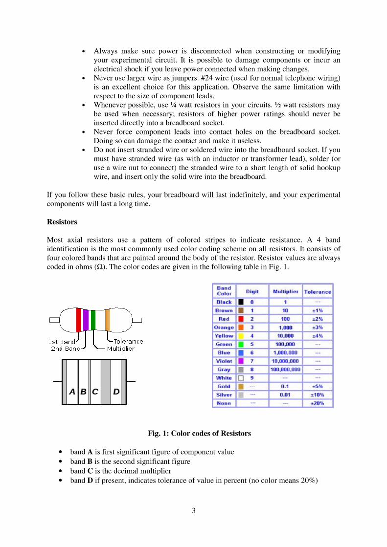
Resistors
Most axial resistors use a pattern of colored stripes to indicate resistance. A 4 band
identification is the most commonly used color coding scheme on all resistors. It consists of
four colored bands that are painted around the body of the resistor. R
coded in ohms (Ω). The color codes are given in the following table in Fig. 1.
• band A is first significant figure of component value
• band B is the second significant figure
• band C is the decimal multiplier
• band D if present, indicates tolerance of value in percent (no color means 20%)
3
Always make sure power is disconnected when constructing or modifying
your experimental circuit. It is possible to damage components or incur
electrical shock if you leave power connected when making changes.
Never use larger wire as jumpers. #24 wire (used for normal telephone wiring)
is an excellent choice for this application. Observe the same limitation with
respect to the size of component leads.
Whenever possible, use ¼ watt resistors in your circuits. ½ watt resistors may
be used when necessary; resistors of higher power ratings should never be
inserted directly into a breadboard socket.
Never force component leads into contact holes on the breadboard socket.
Doing so can damage the contact and make it useless.
Do not insert stranded wire or soldered wire into the breadboard socket. If you
must have stranded wire (as with an inductor or transformer lead), solder (or
use a wire nut to connect) the stranded wire to a short length of solid hookup
wire, and insert only the solid wire into the breadboard.
If you follow these basic rules, your breadboard will last indefinitely, and your experimental
components will last a long time.
Most axial resistors use a pattern of colored stripes to indicate resistance. A 4 band
identification is the most commonly used color coding scheme on all resistors. It consists of
four colored bands that are painted around the body of the resistor. Resistor values are always
). The color codes are given in the following table in Fig. 1.
Fig. 1: Color codes of Resistors
is first significant figure of component value
is the second significant figure
is the decimal multiplier
if present, indicates tolerance of value in percent (no color means 20%)
Always make sure power is disconnected when constructing or modifying
your experimental circuit. It is possible to damage components or incur an
electrical shock if you leave power connected when making changes.
Never use larger wire as jumpers. #24 wire (used for normal telephone wiring)
is an excellent choice for this application. Observe the same limitation with
Whenever possible, use ¼ watt resistors in your circuits. ½ watt resistors may
be used when necessary; resistors of higher power ratings should never be
s on the breadboard socket.
Do not insert stranded wire or soldered wire into the breadboard socket. If you
must have stranded wire (as with an inductor or transformer lead), solder (or
o connect) the stranded wire to a short length of solid hookup
If you follow these basic rules, your breadboard will last indefinitely, and your experimental
Most axial resistors use a pattern of colored stripes to indicate resistance. A 4 band
identification is the most commonly used color coding scheme on all resistors. It consists of
esistor values are always
). The color codes are given in the following table in Fig. 1.
if present, indicates tolerance of value in percent (no color means 20%)

4
For example, a resistor with bands of yellow, violet, red, and gold will have first digit 4
(yellow in table below), second digit 7 (violet), followed by 2 (red) zeros: 4,700 ohms. Gold
signifies that the tolerance is ±5%, so the real resistance could lie anywhere between 4,465
and 4,935 ohms.
Tight tolerance resistors may have three bands for significant figures rather than two, and/or
an additional band indicating temperature coefficient, in units of ppm/K. For large power
resistors and potentiometers, the value is usually written out implicitly as "10 kΩ", for
instance.
Capacitors:
You will mostly use electrolytic and ceramic capacitors for your experiments.
Electrolytic capacitors
An electrolytic capacitor is a type of capacitor that uses an electrolyte, an ionic conducting
liquid, as one of its plates, to achieve a larger capacitance per unit volume than other types.
They are used in relatively high-current and low-
frequency electrical circuits. However, the voltage
applied to these capacitors must be polarized; one
specified terminal must always have positive
potential with respect to the other. These are of two
types, axial and radial capacitors as shown in
adjacent figure. The arrowed stripe indicates the
polarity, with the arrows pointing towards the
negative pin.
Fig. 2:Axial and Radial Electrolytic capacitors
Warning: connecting electrolytic capacitors in reverse polarity can easily damage or destroy
the capacitor. Most large electrolytic capacitors have the voltage, capacitance, temperature
ratings, and company name written on them without having any special color coding
schemes.
Axial electrolytic capacitors have connections on both ends. These are most frequently used
in devices where there is no space for vertically mounted capacitors.
Radial electrolytic capacitors are like axial electrolytic ones, except both pins come out the
same end. Usually that end (the "bottom end") is mounted flat against the PCB and the
capacitor rises perpendicular to the PCB it is mounted on. This type of capacitor probably
accounts for at least 70% of capacitors in consumer electronics.
Ceramic capacitors are generally non-polarized and almost as
common as radial electrolytic capacitors. Generally, they use an
alphanumeric marking system. The number part is the same as for SMT
resistors, except that the value represented is in pF. They may also be
written out directly, for instance, 2n2 = 2.2 nF.
Fig. 3: Ceramic capacitors

5
Diodes:
A standard specification sheet usually has a brief description of the diode. Included in this
description is the type of diode, the major area of application, and any special features. Of
particular interest is the specific application for which the diode is suited. The manufacturer
also provides a drawing of the diode which gives dimension, weight, and, if appropriate, any
identification marks. In addition to the above data, the following information is also
provided: a static operating table (giving spot values of parameters under fixed conditions),
sometimes a characteristic curve (showing how parameters vary over the full operating
range), and diode ratings (which are the limiting values of operating conditions outside which
could cause diode damage). Manufacturers specify these various diode operating parameters
and characteristics with "letter symbols" in accordance with fixed definitions. The following
is a list, by letter symbol, of the major electrical characteristics for the rectifier and signal
diodes.
RECTIFIER DIODES
DC BLOCKING VOLTAGE [VR]—the maximum reverse dc voltage that will not cause
breakdown.
AVERAGE FORWARD VOLTAGE DROP [VF(AV)]—the average forward voltage drop
across the rectifier given at a specified forward current and temperature.
AVERAGE RECTIFIER FORWARD CURRENT [IF(AV)]—the average rectified forward
current at a specified temperature, usually at 60 Hz with a resistive load.
AVERAGE REVERSE CURRENT [IR(AV)]—the average reverse current at a specified
temperature, usually at 60 Hz.
PEAK SURGE CURRENT [ISURGE]—the peak current specified for a given number of cycles
or portion of a cycle.
SIGNAL DIODES
PEAK REVERSE VOLTAGE [PRV]—the maximum reverse voltage that can be applied
before reaching the breakdown point. (PRV also applies to the rectifier diode.)
REVERSE CURRENT [IR]—the small value of direct current that flows when a
semiconductor diode has reverse bias.
MAXIMUM FORWARD VOLTAGE DROP AT INDICATED FORWARD CURRENT [V
F@IF]— the maximum forward voltage drop across the diode at the indicated forward current.
REVERSE RECOVERY TIME [trr]—the maximum time taken for the forward-bias diode to
recover its reverse bias.
The ratings of a diode (as stated earlier) are the limiting values of operating conditions, which
if exceeded could cause damage to a diode by either voltage breakdown or overheating.
The PN junction diodes are generally rated for: MAXIMUM AVERAGE FORWARD
CURRENT, PEAK RECURRENT FORWARD CURRENT, MAXIMUM SURGE
CURRENT, and PEAK REVERSE VOLTAGE
Maximum average forward current is usually given at a special temperature, usually 25º C,
(77º F) and refers to the maximum amount of average current that can be permitted to flow in
the forward direction. If this rating is exceeded, structure breakdown can occur.
Peak recurrent forward current is the maximum peak current that can be permitted to flow
in the forward direction in the form of recurring pulses.
Maximum surge current is the maximum current permitted to flow in the forward direction
in the form of nonrecurring pulses. Current should not equal this value for more than a few
milliseconds.

6
Peak reverse voltage (PRV) is one of the most important ratings. PRV indicates the
maximum reverse-bias voltage that may be applied to a diode without causing junction
breakdown. All of the above ratings are subject to change with temperature variations. If, for
example, the operating temperature is above that stated for the ratings, the ratings must be
decreased.
There are many types of diodes varying in size from the size of a pinhead (used in
subminiature circuitry) to large 250-ampere diodes (used in high-power circuits). Because
there are so many different types of diodes, some system of identification is needed to
distinguish one diode from another. This is accomplished with the semiconductor
identification system shown in Fig. 4. This system is not only used for diodes but transistors
and many other special semiconductor devices as well. As illustrated in this figure, the system
uses numbers and letters to identify different types of semiconductor devices. The first
number in the system indicates the number of junctions in the semiconductor device and is a
number, one less than the number of active elements. Thus 1 designates a diode; 2 designates
a transistor (which may be considered as made up of two diodes); and 3 designates a tetrode
(a four-element transistor). The letter "N" following the first number indicates a
semiconductor. The 2- or 3-digit number following the letter "N" is a serialized identification
number. If needed, this number may contain a suffix letter after the last digit. For example,
the suffix letter "M" may be used to describe matching pairs of separate semiconductor
devices or the letter "R" may be used to indicate reverse polarity. Other letters are used to
indicate modified versions of the device which can be substituted for the basic numbered
unit. For example, a semiconductor diode designated as type 1N345A signifies a two-element
diode (1) of semiconductor material (N) that is an improved version (A) of type 345.
Fig. 4: Identification of Diode Fig. 5: Identification of Cathode
When working with different types of diodes, it is also necessary to distinguish one
end of the diode from the other (anode from cathode). For this reason, manufacturers
generally code the cathode end of the diode with a "k," "+," "cath," a color dot or band, or by
an unusual shape (raised edge or taper) as shown in Fig. 5. In some cases, standard color code
bands are placed on the cathode end of the diode. This serves two purposes: (1) it identifies

the cathode end of the diode, and (2) it also serves to
Transistors:
Transistors are identified by a Joint Army
case of the transistor. If in doubt about a transistor's markings, always replace a transistor
with one having identical markings, or consul
that an identical replacement or substitute is used.
Example:
2 NUMBER OF JUNCTIONS SEMI
(TRANSISTOR)
There are three main series of transistor codes used
• Codes beginning with B (or A), for example BC108, BC478
The first letter B is for silicon, A is for germanium (rarely used now). The second
letter indicates the type; for example C means low power audio frequency; D means
high power audio frequency; F means low power high frequency. The rest of the code
identifies the particular transistor. There is no obvious logic to the numbering system.
Sometimes a letter is added to the end (eg BC108C) to identify a special version of
the main type, for example a higher current gain or a different case style. If a project
specifies a higher gain version (BC108C) it must be used, but if the general code is
given (BC108) any transistor with that code is suitable.
• Codes beginning with TIP, for example TIP31A
TIP refers to the manufacturer: Texas Instruments Power transistor.
end identifies versions with different voltage ratings.
• Codes beginning with 2N, for example 2N3053
The initial '2N' identifies the part as a transistor and the rest of the code identifies the
particular transistor. There is no obvious logic to the numbering system.
TESTING A TRANSISTOR
good or bad can be done with an ohmmeter or
transistor tester. PRECAUTIONS
when working with transistors since they are
susceptible to damage by electrical overloads, heat,
humidity, and radiation. TRANSISTOR LEAD
IDENTIFICATION plays an important part in
transistor maintenance because before a transistor
can be tested or replaced, its leads must be
identified. Since there is NO standard method of
identifying transistor leads, check some typical
lead identification schemes or a transistor manual
before attempting to replace a transis
Identification of leads for some common case
styles is shown in Fig. 6.
Fig. 6
7
the cathode end of the diode, and (2) it also serves to identify the diode by number.
by a Joint Army-Navy (JAN) designation printed directly on
case of the transistor. If in doubt about a transistor's markings, always replace a transistor
with one having identical markings, or consult an equipment or transistor manual to ensure
that an identical replacement or substitute is used.
2 N 130 SEMICONDUCTOR IDENTIFICATION FIRST MODIFICATION
NUMBER
There are three main series of transistor codes used:
Codes beginning with B (or A), for example BC108, BC478
The first letter B is for silicon, A is for germanium (rarely used now). The second
letter indicates the type; for example C means low power audio frequency; D means
high power audio frequency; F means low power high frequency. The rest of the code
ies the particular transistor. There is no obvious logic to the numbering system.
Sometimes a letter is added to the end (eg BC108C) to identify a special version of
the main type, for example a higher current gain or a different case style. If a project
pecifies a higher gain version (BC108C) it must be used, but if the general code is
given (BC108) any transistor with that code is suitable.
Codes beginning with TIP, for example TIP31A
TIP refers to the manufacturer: Texas Instruments Power transistor.
end identifies versions with different voltage ratings.
Codes beginning with 2N, for example 2N3053
The initial '2N' identifies the part as a transistor and the rest of the code identifies the
particular transistor. There is no obvious logic to the numbering system.
to determine if it is
good or bad can be done with an ohmmeter or
PRECAUTIONS should be taken
when working with transistors since they are
damage by electrical overloads, heat,
TRANSISTOR LEAD
plays an important part in
use before a transistor
can be tested or replaced, its leads must be
identified. Since there is NO standard method of
identifying transistor leads, check some typical
lead identification schemes or a transistor manual
before attempting to replace a transistor.
leads for some common case
by number.
Navy (JAN) designation printed directly on the
case of the transistor. If in doubt about a transistor's markings, always replace a transistor
t an equipment or transistor manual to ensure
130 A MODIFICATION
Codes beginning with B (or A), for example BC108, BC478 The first letter B is for silicon, A is for germanium (rarely used now). The second
letter indicates the type; for example C means low power audio frequency; D means
high power audio frequency; F means low power high frequency. The rest of the code
ies the particular transistor. There is no obvious logic to the numbering system.
Sometimes a letter is added to the end (eg BC108C) to identify a special version of
the main type, for example a higher current gain or a different case style. If a project
pecifies a higher gain version (BC108C) it must be used, but if the general code is
Codes beginning with TIP, for example TIP31A TIP refers to the manufacturer: Texas Instruments Power transistor. The letter at the
Codes beginning with 2N, for example 2N3053 The initial '2N' identifies the part as a transistor and the rest of the code identifies the
particular transistor. There is no obvious logic to the numbering system.

Testing a transistor
Transistors are basically made up of two
can use this analogy to determine whether a transistor
its Resistance between the three different leads,
Emitter, Base and Collector.
Testing with a multimeter
Use a multimeter or a simple tester
and LED) to check each pair of leads for conduction.
Set a digital multimeter to diode test and an analogue
multimeter to a low resistance range.
Test each pair of leads both ways
• The base-emitter (BE)
like a diode and conduct one way only
• The base-collector (BC)
behave like a diode and
• The collector-emitter (CE)
The diagram shows how the junctions behave in an NPN tran
in a PNP transistor but the same test procedure can be used.
Transistor Resistance Values for the PNP and NPN transistor types
Between Transistor Terminals
Collector
Collector
Emitter
Emitter
Base
Base
8
Transistors are basically made up of two Diodes connected together back-to
can use this analogy to determine whether a transistor is of the type PNP or NPN by testing
its Resistance between the three different leads,
Testing with a multimeter
tester (battery, resistor
and LED) to check each pair of leads for conduction.
Set a digital multimeter to diode test and an analogue
multimeter to a low resistance range.
Test each pair of leads both ways (six tests in total):
emitter (BE) junction should behave
conduct one way only.
collector (BC) junction should
behave like a diode and conduct one way only.
emitter (CE) should not conduct either way.
The diagram shows how the junctions behave in an NPN transistor. The diodes are reversed
in a PNP transistor but the same test procedure can be used.
Transistor Resistance Values for the PNP and NPN transistor types
Between Transistor Terminals PNP NPN
Emitter RHIGH R
Base RLOW R
Collector RHIGH R
Base RLOW R
Collector RHIGH R
Emitter RHIGH R
Fig. 7: Testing an NPN transistor
to-back (Fig. 7). We
is of the type PNP or NPN by testing
sistor. The diodes are reversed
Transistor Resistance Values for the PNP and NPN transistor types
NPN
RHIGH
RHIGH
RHIGH
RHIGH
RLOW
RLOW
Fig. 7: Testing an NPN transistor
9
Bipolar Junction Transistor Static Characteristics
Objective:
(i) To study the input and output characteristics of a PNP transistor in Common Base
mode and determine transistor parameters.
(ii) To study the input and output characteristics of an NPN transistor in Common
Emitter mode and determine transistor parameters.
Overview:
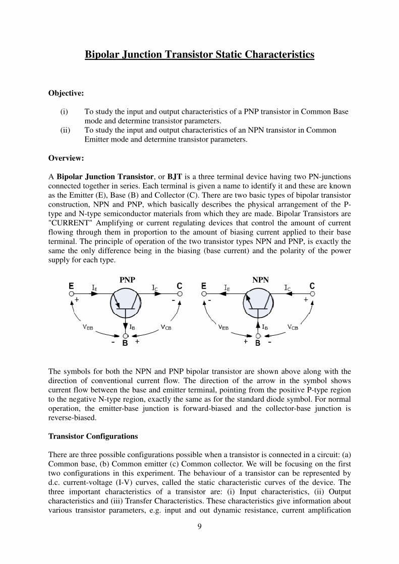
A Bipolar Junction Transistor, or BJT is a three terminal device having two PN-junctions
connected together in series. Each terminal is given a name to identify it and these are known
as the Emitter (E), Base (B) and Collector (C). There are two basic types of bipolar transistor
construction, NPN and PNP, which basically describes the physical arrangement of the P-
type and N-type semiconductor materials from which they are made. Bipolar Transistors are
"CURRENT" Amplifying or current regulating devices that control the amount of current
flowing through them in proportion to the amount of biasing current applied to their base
terminal. The principle of operation of the two transistor types NPN and PNP, is exactly the
same the only difference being in the biasing (base current) and the polarity of the power
supply for each type.
The symbols for both the NPN and PNP bipolar transistor are shown above along with the
direction of conventional current flow. The direction of the arrow in the symbol shows
current flow between the base and emitter terminal, pointing from the positive P-type region
to the negative N-type region, exactly the same as for the standard diode symbol. For normal
operation, the emitter-base junction is forward-biased and the collector-base junction is
reverse-biased.
Transistor Configurations
There are three possible configurations possible when a transistor is connected in a circuit: (a)
Common base, (b) Common emitter (c) Common collector. We will be focusing on the first
two configurations in this experiment. The behaviour of a transistor can be represented by
d.c. current-voltage (I-V) curves, called the static characteristic curves of the device. The
three important characteristics of a transistor are: (i) Input characteristics, (ii) Output
characteristics and (iii) Transfer Characteristics. These characteristics give information about
various transistor parameters, e.g. input and out dynamic resistance, current amplification
PNP NPN
10
factors, etc.
Common Base Transistor Characteristics
In common base configuration, the base is made common to both input and output as shown
in its circuit diagram.
(1) Input Characteristics: The input characteristics is obtained by plotting a curve between IE
and VEB keeping voltage VCB constant. This is very similar to that of a forward-biased diode
and the slope of the plot at a given operating point gives information about its input dynamic
resistance.
Input Dynamic Resistance (ri) This is defined as the ratio of change in base emitter voltage
(∆VEB) to the resulting change in emitter current (∆IE) at constant collector-emitter voltage
(VCB). This is dynamic as its value varies with the operating current in the transistor.
CBVE
EB
iI
Vr
∆∆∆∆
∆∆∆∆====
(2) Output Characteristics: The output characteristic curves are plotted between IC and VCB,
keeping IE constant. The output characteristics are controlled by the input characteristics.
Since IC changes with IE, there will be different output characteristics corresponding to
different values of IE. These curves are almost horizontal. This shows that the output dynamic
resistance, defined below, is very high.
Output Dynamic Resistance (ro): This is defined as the ratio of change in collector-base
voltage (∆VCB) to the change in collector current (∆IC) at a constant base current IE.
EIC
CB
oI
Vr
∆∆∆∆
∆∆∆∆====
(3) Transfer Characteristics: The transfer characteristics are plotted between the input and
output currents (IE versus IC).
Current amplification factor (α)
This is defined as the ratio of the change in collector current to the change in emitter current
at a constant collector-base voltage (VCB) when the transistor is in active state.
CBVE
Cac
I
I
∆∆∆∆
∆∆∆∆====αααα
This is also known as small signal current gain and its value is very large. The ratio of IC and
IE is called αdc of the transistor. Hence,
11
CBVE
Cdc
I
I====αααα
Since IC increases with IE almost linearly, the values of both αdc and αac are nearly equal.
Common Emitter Transistor Characteristics
In a common emitter configuration, emitter is common to both input and output as shown in
its circuit diagram.
(1) Input Characteristics: The variation of the base current IB with the base-emitter voltage
VBE keeping the collector-emitter voltage VCE fixed, gives the input characteristic in CE
mode.
Input Dynamic Resistance (ri): This is defined as the ratio of change in base emitter voltage
(∆VBE) to the resulting change in base current (∆IB) at constant collector-emitter voltage
(VCE). This is dynamic and it can be seen from the input characteristic, its value varies with
the operating current in the transistor:
CEVB
BEi
I
Vr
∆∆∆∆
∆∆∆∆====
The value of ri can be anything from a few hundreds to a few thousand ohms.
(2) Output Characteristics: The variation of the collector current IC with the collector-emitter
voltage VCE is called the output characteristic. The plot of IC versus VCE for different fixed
values of IB gives one output characteristic. Since the collector current changes with the base
current, there will be different output characteristics corresponding to different values of IB.
Output Dynamic Resistance (ro): This is defined as the ratio of change in collector-emitter
voltage (∆VCE) to the change in collector current (∆IC) at a constant base current IB.
BIC
CE
oI
Vr
∆∆∆∆
∆∆∆∆====
The high magnitude of the output resistance (of the order of 100 kW) is due to the reverse-
biased state of this diode.
(3) Transfer Characteristics: The transfer characteristics are plotted between the input and
output currents (IB versus IC). Both IB and IC increase proportionately.
Current amplification factor (β)
This is defined as the ratio of the change in collector current to the change in base current at a
constant collector-emitter voltage (VCE) when the transistor is in active state.

12
CEVB
Cac
I
I
∆∆∆∆
∆∆∆∆====ββββ
This is also known as small signal current gain and its value is very large. The ratio of IC and
IB we get what is called βdc of the transistor. Hence,
CEVB
C
dcI
I====ββββ
Since IC increases with IB almost linearly, the values of both βdc and βac are nearly equal.
Circuit components/Equipments:
(i) Transistors (2 Nos: 1 PNP (CK 100 or equivalent) and 1 NPN (BC 107 or equivalent)), (ii)
Resistors (4 Nos.) (iii) Multimeters (3 Nos.), (iv) D.C. power supply, (v) Connecting wires
and (vi) Breadboard.
Circuit Diagrams:
PNP transistor in CB configuration
NPN transistor in CE configuration
Procedure:
1. Note down the type number of both the transistors.
2. Identify different terminals (E, B and C) and the type (PNP/NPN) of the transistors. For
any specific information refer the datasheet of the transistors.

13
(I) PNP Common Base (CB) characteristics
1. Configure CB circuit using the PNP transistor as per the circuit diagram. Use RE = RC =
150 Ω.
2. For input characteristics, first fix the voltage VCB by adjusting VCC to the minimum
possible position. Now vary the voltage VEB slowly (say, in steps of 0.05V) by varying
VEE. Measure VEB using a multimeter. If VCB varies during measurement bring it back to
the initial set value To determine IE, measure VRE across the resistor RE and use the
relation IE = VRE/RE.
3. Repeat the above step for another value of VCB say, 2V.
4. Take out the multimeter measuring VEB and connect in series with the output circuit to
measure IC. For output characteristics, first fix IE = 0, i.e. VRE = 0. By adjusting VCC, vary
the collector voltage VCB in steps of say 1V and measure VCB and the corresponding IC
using multimeters. After acquiring sufficient readings, bring back VCB to 0 and reduce it
further to get negative values. Vary VCB in negative direction and measure both VCB and
IC, till you get 0 current.
5. Repeat the above step for at least 5 different values of IE by adjusting VEE. You may need
to adjust VEE continuously during measurement in order to maintain a constant IE.
6. Plot the input and output characteristics by using the readings taken above and determine
the input and output dynamic resistance.
7. To plot transfer characteristics, select a suitable voltage VCB well within the active region
of the output characteristics, which you have tabulated already. Plot a graph between IC
and the corresponding IE at the chosen voltage VCB. Determine αac from the slope of this
graph.
(II) NPN Common Emitter (CE) characteristics
1. Now configure CE circuit using the NPN transistor as per the circuit diagram. Use RB =
100kΩ and RC = 1 kΩ.
2. For input characteristics, first fix the voltage VCE by adjusting VCC to the minimum
possible position. Now vary the voltage VBE slowly (say, in steps of 0.05V) by varying
VBB. Measure VBE using a multimeter. If VCE varies during measurement bring it back to
the set value To determine IB, measure VRB across the resistor RB and use the relation IB =
VRB/RB.
3. Repeat the above step for another value of VCE say, 2V.

14
4. For output characteristics, first fix IB = 0, i.e. VRB = 0. By adjusting VCC, vary the
collector voltage VCE in steps of say 1V and measure VCE and the corresponding IC using
multimeters. If needed vary VCE in negative direction as described for CB configuration
and measure both VCE and IC, till you get 0 current.
5. Repeat the above step for at least 5 different values of IB by adjusting VBB. You may need
to adjust VBB continuously during measurement in order to maintain a constant IB.
6. Plot the input and output characteristics by using the readings taken above and determine
the input and output dynamic resistance.
7. Plot the transfer characteristics between IC and IB as described for CB configuration for a
suitable voltage of VCE on the output characteristics. Determine βac from the slope of this
graph.
Observations:
CB configuration:
Transistor code: ________, Transistor type: ______ (PNP/NPN)
RE = _____, RC = ________.
Table (1): Input Characteristics
Sl. No. VCB = ___V VCB = ___V
VEB (V) VRE (V) IE (mA) VEB (V) VRE (V) IE (mA)
1
2
..
..
10
Table (2): Output Characteristics
Sl.
No.
IE1 = 0 IE2 = __ IE3 = __ IE4 = __ IE5 = __
VCB
(V)
IC
(mA)
VCB
(V)
IC
(mA)
VCB
(V)
IC
(mA)
VCB
(V)
IC
(mA)
VCB
(V)
IC
(mA)
1
2
..
..
10
15
Table (3): Transfer Characteristics VCB = _______ V
Sl. No. IE (mA) IC (mA)
1
2
3
4
5
CE configuration: Transistor code: ________, Transistor type: ______ (PNP/NPN)
RB = _____, RC = ________.
Table (5): Input Characteristics
Sl. No. VCE = ___V VCE = ___V
VBE (V) VRB (V) IB (μA) VBE (V) VRB (V) IB (μA)
1
2
..
..
10
Table (4): Output Characteristics
Sl.
No.
IB1 = 0 IB2 = __ IB3 = __ IB4 = __ IB5 = __
VCE
(V)
IC
(mA)
VCE
(V)
IC
(mA)
VCE
(V)
IC
(mA)
VCE
(V)
IC
(mA)
VCE
(V)
IC
(mA)
1
2
..
..
10
Table (6): Transfer Characteristics VCE = _______ V
Sl. No. IB (μA) IC (mA)
1
2
3
4
5

16
Graphs:
Plot the input, output and transfer characteristics for each configuration.
CB configuration:
(1) Input characteristics: Plot VEB ~ IE, for different VCB and determine the input dynamic
resistance in each case at suitable operating points.
(2) Output characteristics: Plot VCB ~ IC, for different IE and determine the output
dynamic resistance in each case at suitable operating points in the active region.
(3) Transfer characteristics: Plot IE ~ IC, for a fixed VCB and determine αac.
CE configuration:
(1) Input characteristics: Plot VBE ~ IB, for different VCE and determine the input dynamic
resistance in each case at suitable operating points.
(2) Output characteristics: Plot VCE ~ IC, for different IB and determine the output
dynamic resistance in each case at suitable operating points in the active region.
(3) Transfer characteristics: Plot IB ~ IC, for a fixed VCE and determine βac.
Results/Discussions:
Precautions:
________________________________________________________________________
17
Study of Common Emitter Transistor Amplifier circuit
Objectives:
1. To design a common emitter transistor (NPN) amplifier circuit.
2. To obtain the frequency response curve of the amplifier and to determine the mid-
frequency gain, Amid, lower and higher cutoff frequency of the amplifier circuit.
Overview:
The most common circuit configuration for an NPN transistor is that of the Common Emitter
Amplifier and that a family of curves known commonly as the Output Characteristics Curves,
relates the Collector current (IC), to the output or Collector voltage (VCE), for different values
of Base current (IB). All types of transistor amplifiers operate using AC signal inputs which
alternate between a positive value and a negative value. Presetting the amplifier circuit to
operate between these two maximum or peak values is achieved using a process known as
Biasing. Biasing is very important in amplifier design as it establishes the correct operating
point of the transistor amplifier ready to receive signals, thereby reducing any distortion to
the output signal.
The single stage common emitter amplifier circuit shown below uses what is commonly
called "Voltage Divider Biasing". The Base voltage (VB) can be easily calculated using the
simple voltage divider formula below:
21
2
RR
RVV CC
B++++
====
Thus the base voltage is fixed by biasing and independent of base current provided the
current in the divider circuit is large compared to the base current. Thus assuming IB ≈0, one
can do the approximate analysis of the voltage divider network without using the transistor
gain, β, in the calculation. Note that the approximate approach can be applied with a high
degree of accuracy when the following condition is satisfied:
210RRE ≥≥≥≥ββββ

18
Load line and Q-point
A static or DC load line can be drawn onto the output characteristics curves of the transistor
to show all the possible operating points of the transistor from fully "ON" (IC = VCC/(RC +
RE)) to fully "OFF" (IC = 0). The quiescent operating point or Q-point is a point on this load
line which represents the values of IC and VCE that exist in the circuit when no input signal is
applied. Knowing VB, IC and VCE can be calculated to locate the operating point of the circuit
as follows:
BEBE VVV −−−−====
So, the emitter current,
E
E
CER
VII ====≈≈≈≈
and )( ECCCCCE RRIVV ++++−−−−====
It can be noted here that the sequence of calculation does not need the knowledge of β and IB
is not calculated. So the Q-point is stable against any replacement of the transistor.
Since the aim of any small signal amplifier is to generate an amplified input signal at the
output with minimum distortion possible, the best position for this Q-point is as close to the
centre position of the load line as reasonably possible, thereby producing a Class A type
amplifier operation, i.e. VCE = 1/2VCC.
Coupling and Bypass Capacitors
In CE amplifier circuits, capacitors C1 and C2 are used as Coupling Capacitors to separate the
AC signals from the DC biasing voltage. The capacitors will only pass AC signals and block
any DC component. Thus they allow coupling of the AC signal into an amplifier stage
without disturbing its Q point. The output AC signal is then superimposed on the biasing of
the following stages. Also a bypass capacitor, CE is included in the Emitter leg circuit. This
capacitor is an open circuit component for DC bias, meaning that the biasing currents and
voltages are not affected by the addition of the capacitor maintaining a good Q-point stability.
However, this bypass capacitor acts as a short circuit path across the emitter resistor at high
frequency signals increasing the voltage gain to its maximum. Generally, the value of the
bypass capacitor, CE is chosen to provide a reactance of at most, 1/10th the value of RE at the
lowest operating signal frequency.
Amplifier Operation
Once the Q-point is fixed through DC bias, an AC signal is applied at the input using
coupling capacitor C1. During positive half cycle of the signal VBE increases leading to
increased IB. Therefore IC increases by β times leading to decrease in the output voltage, VCE.
Thus the CE amplifier produces an amplified output with a phase reversal. The voltage Gain
of the common emitter amplifier is equal to the ratio of the change in the output voltage to the
change in the input voltage. Thus,
BE
CE
in
out
VV
V
V
VA
∆∆∆∆
∆∆∆∆========
The input (Zi) and output (Zo) impedances of the circuit can be computed for the case when
19
the emitter resistor RE is completely bypassed by the capacitor, CE:
Zi = R1 R2βre and Zo = RCro
where re (26mV/IE) and ro are the emitter diode resistance and output dynamic resistance (can
be determined from output characteristics of transistor). Usually ro≥10 RC, thus the gain can
be approximated as
(((( ))))eeB
B
in
out
Vr
R
rI
I
V
VA CoC rR
−−−−≅≅≅≅−−−−========ββββ
ββββ
The negative sign accounts for the phase reversal at the output. In the circuit diagram
provided below, the emitter resistor is split into two in order to reduce the gain to avoid
distortion. So the expression for gain is modified as
)( 1
C
eE
VrR
RA
++++−−−−≅≅≅≅
Frequency Response Curve
The performance of an amplifier is characterized by its frequency response curve that shows
output amplitude (or, more often, voltage gain) plotted versus frequency (often in log scale).
Typical plot of the voltage gain of an amplifier versus frequency is shown in the figure below.
The frequency response of an amplifier can be divided into three frequency ranges.
The frequency response begins with the lower frequency range designated between 0 Hz and
lower cutoff frequency. At lower cutoff frequency, fL , the gain is equal to 0.707 Amid. Amid is a
constant mid-band gain obtained from the mid-frequency range. The third, the higher
frequency range covers frequency between upper cutoff frequency and above. Similarly, at
higher cutoff frequency, fH, the gain is equal to 0.707 Amid. Beyond this the gain decreases
with frequency increases and dies off eventually.
The Lower Frequency Range Since the impedance of coupling capacitors increases as frequency decreases, the voltage
gain of a BJT amplifier decreases as frequency decreases. At very low frequencies, the
capacitive reactance of the coupling capacitors may become large enough to drop some of the
input voltage or output voltage. Also, the emitter-bypass capacitor may become large enough

20
so that it no longer shorts the emitter resistor to ground.
The Higher Frequency Range The capacitive reactance of a capacitor decreases as frequency increases. This can lead to
problems for amplifiers used for high-frequency amplification. The ultimate high cutoff
frequency of an amplifier is determined by the physical capacitances associated with every
component and of the physical wiring. Transistors have internal capacitances that shunt signal
paths thus reducing the gain. The high cutoff frequency is related to a shunt time constant
formed by resistances and capacitances associated with a node.
Design:
Before designing the circuit, one needs to know the circuit requirement or specifications. The
circuit is normally biased for VCE at the mid-point of load line with a specified collector
current. Also, one needs to know the value of supply voltage VCC and the range of β for the
transistor being used (available in the datasheet of the transistor).
Here the following specifications are used to design the amplifier:
VCC = 12V and IC = 1 mA
Start by making VE= 0.1 VCC. Then RE = VE/IE (Use IE≈IC).
Since VCE = 0.5 VCC, Voltage across RC = 0.4VCC, i.e. RC = 4.RE
In order that the approximation analysis can be applied, ERR ββββ1.02 ≤≤≤≤ . Here ββββ is the
minimum rated value in the specified range provided by the datasheet (in this case ββββ =50).
Finally, 2
2
1
1 RV
VR ==== , V1 (= VCC-V2)and V2 (= VE+VBE) are voltages across R1 and R2,
respectively.
Based on these guidelines the components are estimated and the nearest commercially
available values are used.
Components/ Equipments:
1. Transistor: CL100 (or equivalent general purpose npn)
2. Resistors: R1= 26 (27) KΩ, R2= 5 (4.7+0.22) KΩ, RC = 4 (3.9) KΩ, RE= 1kΩ (RE1=470 Ω,
RE2=560 Ω)
3. Capacitors: C1= C2= 1 μF (2 nos.), CE= 100μF
4. Power Supply (VCC = 12V)
5. Oscilloscope
6. Function Generator (~ 100-200 mV pp, sinusoidal for input signal)
7. Breadboard
8. Connecting wires
Circuit Diagram:
21
Procedure:
1. Measure and record all the values of resistance and capacitance and β of the transistor
using a multimeter. Configure the circuit as per the diagram.
2. Apply supply voltage to the circuit. Measure and record all the dc parameters listed in
Table 1 in absence of the ac signal.
3. Next, set the function generator in 20Hz “Frequency” range. Also, set the “Attenuation”
button at 40dB. Connect the output to the oscilloscope and adjust the “Amplitude” knob
till you get a sinusoidal input signal, Vi ≈ 100-200 mV peak-to-peak value. DO NOT
CHANGE THIS SETTING THROUGHOUT THE EXPERIMENT.
4. Now apply this input signal to the circuit you have made keeping the connection to
oscilloscope in tact. Feed the output of the circuit to the other channel of oscilloscope.
Take care to make all the ground pins common.
5. With input signal amplitude always constant, increase signal frequency slowly. Observe,
measure and record the output voltage, Vo. Scan the entire frequency in the range 20 Hz –
2 MHz. You may have to measure Vi and take the ratio Vo/Vi each time in case input
fluctuation is too large to hold constant.
6. Calculate the voltage gain for each frequency. Observe the inverted output.
7. Plot the frequency response curve, i.e. voltage gain in dB versus frequency on a semi-log
graph-sheet.
8. Estimate the mid-frequency gain and also the lower and higher cut off frequencies and
hence the bandwidth.
Observations:
β = _____________
R1= ____, R2= ____, RC= ____, RE= ____; C1= ___, C2= ___, CE= ___

22
Table 1: D.C. analysis of the circuit
VCC = 12V
Parameter Computed value Observed value
VB (V)
VE (V)
IC≈IE (mA)
VCE (V)
Q-point is at (__V, __mA)
Table 2: Frequency response
Vi(pp) = ___ mV
Sl.
No.
Frequency,
f (kHz)
V0(pp)
(Volt)
Gain,AV=
)(
)(
ppV
ppV
i
o
Gain
(dB)
1
2
..
..
Calculations: re = _____ , Zi = _______, Zo = _________ Theoretical value of Av in mid-frequency range = _______
Graphs: Plot the frequency response curve (semi-log plot) and determine the cut-off
frequencies, bandwidth and mid- frequency gain.
Discussions:
Precautions:
1. Vary the input signal frequency slowly.
2. Connect electrolytic capacitors carefully.
Reference: Electronic devices and circuit theory, Robert L. Boylestad & Louis Nashelsky
(10th
Edition)

23
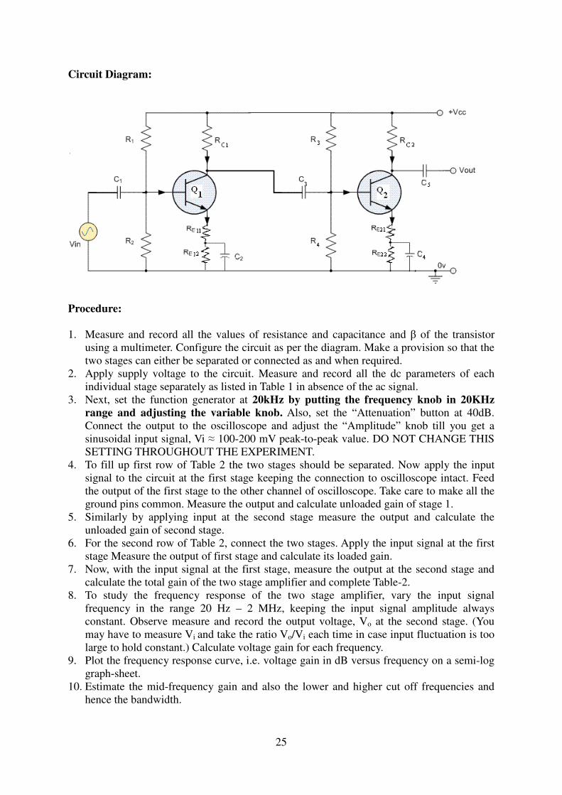
Two Stage RC Coupled Transistor Amplifier
Objective:
1. To design a two stage RC coupled common emitter transistor (NPN) amplifier circuit and
to study its frequency response curve.
Overview:
A single stage of amplification is often not enough for a particular application. The overall
gain can be increased by using more than one stage, so when two amplifiers are connected in
such a way that the output signal of the first serves as the input signal to the second, the
amplifiers are said to be connected in cascade. The most common arrangement is the
common-emitter configuration.
Resistance-capacitance (RC) coupling is most widely used to connect the output of first stage to
the input (base) of the second stage and so on. It is the most popular type of coupling because it is
cheap and provides a constant amplification over a wide range of frequencies. These R-C
coupled amplifier circuits are commonly used as voltage amplifiers in the audio systems.
The circuit diagram above shows the 2-stages of an R-C coupled amplifier in CE
configuration using NPN transistors. Capacitors C1 and C3 couple the input signal to
transistors Q1 and Q2, respectively. C5 is used for coupling the signal from Q2 to its load. R1,
R2, RE1 and R3, R4, RE2 are used for biasing and stabilization of stage 1 and 2 of the amplifier.
C2 and C4 provide low reactance paths to the signal through the emitter.
Overall gain:
The total gain of a 2-stage amplifier is equal to the product of individual gain of each stage.
(You may refer to the handout for single stage amplifier to calculate individual gain of the
stages.) Once the second stage is added, its input impedance acts as an additional load on the
first stage thereby reducing the gain as compared to its no load gain. Thus the overall gain
characteristics is affected due to this loading effect.
The loading of the second stage i.e. input impedance of second stage, Zi2 = R3 R4βre2
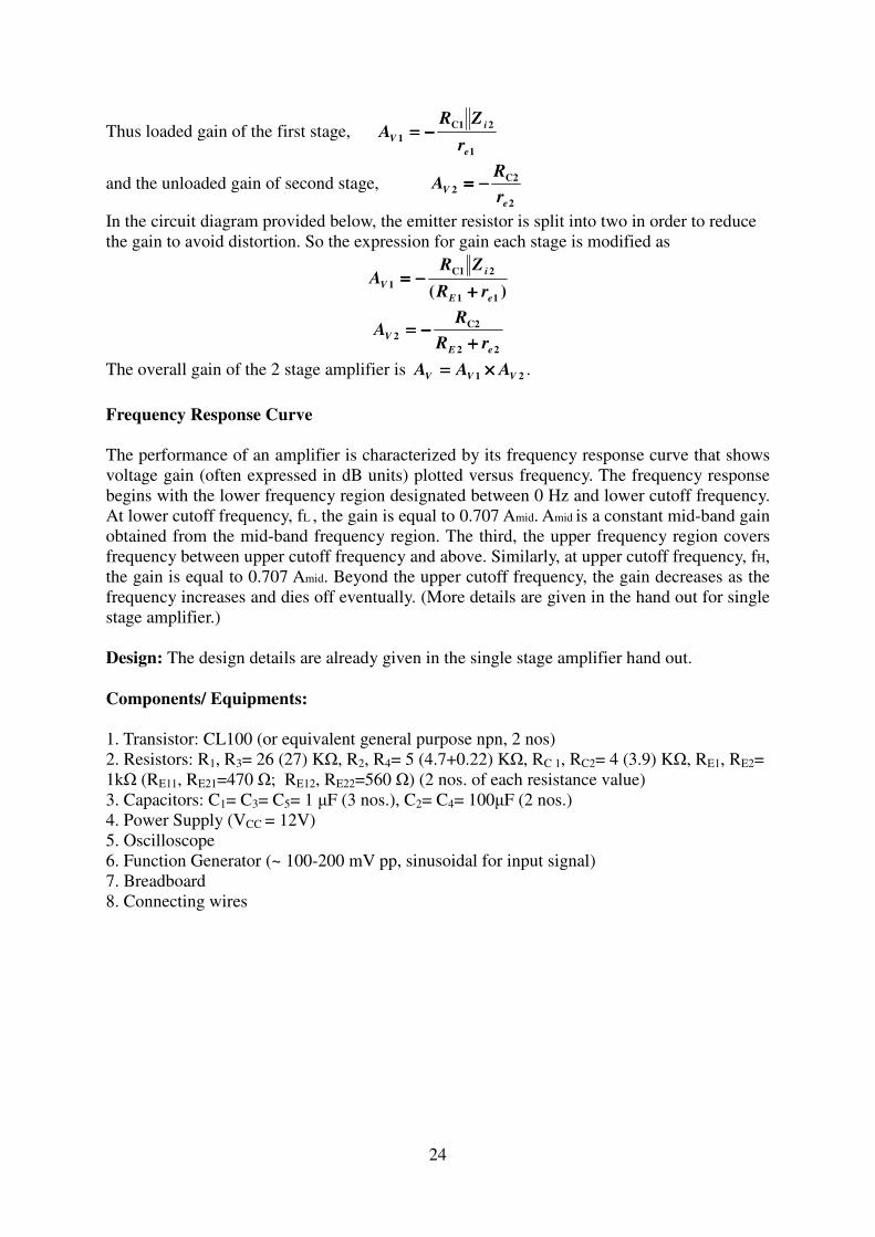
24
Thus loaded gain of the first stage, 1
2C1
1
e
i
Vr
ZRA −−−−====
and the unloaded gain of second stage, 2
C2
2
e
Vr
RA −−−−====
In the circuit diagram provided below, the emitter resistor is split into two in order to reduce
the gain to avoid distortion. So the expression for gain each stage is modified as
)( 11
2C1
1
eE
i
VrR
ZRA
++++−−−−====
22
C2
2
eE
VrR
RA
++++−−−−====
The overall gain of the 2 stage amplifier is 21 VVV AAA ××××==== .
Frequency Response Curve
The performance of an amplifier is characterized by its frequency response curve that shows
voltage gain (often expressed in dB units) plotted versus frequency. The frequency response
begins with the lower frequency region designated between 0 Hz and lower cutoff frequency.
At lower cutoff frequency, fL , the gain is equal to 0.707 Amid. Amid is a constant mid-band gain
obtained from the mid-band frequency region. The third, the upper frequency region covers
frequency between upper cutoff frequency and above. Similarly, at upper cutoff frequency, fH,
the gain is equal to 0.707 Amid. Beyond the upper cutoff frequency, the gain decreases as the
frequency increases and dies off eventually. (More details are given in the hand out for single
stage amplifier.)
Design: The design details are already given in the single stage amplifier hand out.
Components/ Equipments:
1. Transistor: CL100 (or equivalent general purpose npn, 2 nos)
2. Resistors: R1, R3= 26 (27) KΩ, R2, R4= 5 (4.7+0.22) KΩ, RC 1, RC2= 4 (3.9) KΩ, RE1, RE2=
1kΩ (RE11, RE21=470 Ω; RE12, RE22=560 Ω) (2 nos. of each resistance value)
3. Capacitors: C1= C3= C5= 1 μF (3 nos.), C2= C4= 100μF (2 nos.)
4. Power Supply (VCC = 12V)
5. Oscilloscope
6. Function Generator (~ 100-200 mV pp, sinusoidal for input signal)
7. Breadboard
8. Connecting wires
25
Circuit Diagram:
Procedure:
1. Measure and record all the values of resistance and capacitance and β of the transistor
using a multimeter. Configure the circuit as per the diagram. Make a provision so that the
two stages can either be separated or connected as and when required.
2. Apply supply voltage to the circuit. Measure and record all the dc parameters of each
individual stage separately as listed in Table 1 in absence of the ac signal.
3. Next, set the function generator at 20kHz by putting the frequency knob in 20KHz
range and adjusting the variable knob. Also, set the “Attenuation” button at 40dB.
Connect the output to the oscilloscope and adjust the “Amplitude” knob till you get a
sinusoidal input signal, Vi ≈ 100-200 mV peak-to-peak value. DO NOT CHANGE THIS
SETTING THROUGHOUT THE EXPERIMENT.
4. To fill up first row of Table 2 the two stages should be separated. Now apply the input
signal to the circuit at the first stage keeping the connection to oscilloscope intact. Feed
the output of the first stage to the other channel of oscilloscope. Take care to make all the
ground pins common. Measure the output and calculate unloaded gain of stage 1.
5. Similarly by applying input at the second stage measure the output and calculate the
unloaded gain of second stage.
6. For the second row of Table 2, connect the two stages. Apply the input signal at the first
stage Measure the output of first stage and calculate its loaded gain.
7. Now, with the input signal at the first stage, measure the output at the second stage and
calculate the total gain of the two stage amplifier and complete Table-2.
8. To study the frequency response of the two stage amplifier, vary the input signal
frequency in the range 20 Hz – 2 MHz, keeping the input signal amplitude always
constant. Observe measure and record the output voltage, Vo at the second stage. (You
may have to measure Vi and take the ratio Vo/Vi each time in case input fluctuation is too
large to hold constant.) Calculate voltage gain for each frequency.
9. Plot the frequency response curve, i.e. voltage gain in dB versus frequency on a semi-log
graph-sheet.
10. Estimate the mid-frequency gain and also the lower and higher cut off frequencies and
hence the bandwidth.

26
Observations:
β1 = _____________ , β2 = _____________
Stage 1: R1= ____, R2= ____, RC= ____, RE= ____+___; C1= ___, C2= ___, CE= ___
Stage 2: R1= ____, R2= ____, RC= ____, RE= ____+___; C1= ___, C2= ___, CE= ___
Table 1: D.C. analysis of the circuit
VCC = 12V
Parameter Stage 1 (Q1) Stage 2 (Q2)
Computed value Observed value Computed value Observed value
VB (V)
VE (V)
IC≈IE (mA)
VCE (V)
re(Ω)
Q-point
Table 2: Mid frequency voltage Gain (f ≈ 20 kHz)
Vi = _________
Parameter Stage 1 (Q1) Stage 2 (Q2)
Computed Measured Computed Measured
Unloaded
Voltage Gain
(Vo/ Vi)
Loaded
Voltage Gain
Total mid frequency gain = Loaded Voltage Gain (Q1) × Unloaded Voltage Gain (Q2)
Total gain (computed) = ________
Total gain (measured) = ________
Table 3: Frequency Response
Vi(pp) = _________
Sl.
No.
Frequency,
f (kHz)
V0(pp)
(Volt)
Gain,AV=
)(
)(
ppV
ppV
i
o
Gain
(dB)
1

27
2
..
..
Calculations: Stage 1: Zi1 = _______, Zo1 = _________
Stage 2: Zi2 = _______, Zo2 = _________
Graphs: Plot the frequency response curve and determine the cut-off frequencies, bandwidth
and mid-band gain.
Discussions:
Precautions:
3. Vary the input signal frequency slowly.
4. Connect electrolytic capacitors carefully.
Reference: Electronic devices and circuit theory, Robert L. Boylestad & Louis Nashelsky
(10th
Edition)
________________________________________________________________________
28
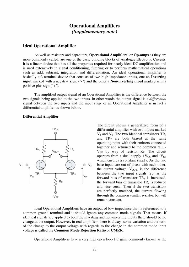
Operational Amplifiers
(Supplementary note)
Ideal Operational Amplifier
As well as resistors and capacitors, Operational Amplifiers, or Op-amps as they are
more commonly called, are one of the basic building blocks of Analogue Electronic Circuits.
It is a linear device that has all the properties required for nearly ideal DC amplification and
is used extensively in signal conditioning, filtering or to perform mathematical operations
such as add, subtract, integration and differentiation. An ideal operational amplifier is
basically a 3-terminal device that consists of two high impedance inputs, one an Inverting
input marked with a negative sign, ("-") and the other a Non-inverting input marked with a
positive plus sign ("+").
The amplified output signal of an Operational Amplifier is the difference between the
two signals being applied to the two inputs. In other words the output signal is a differential
signal between the two inputs and the input stage of an Operational Amplifier is in fact a
differential amplifier as shown below.
Differential Amplifier
The circuit shows a generalized form of a
differential amplifier with two inputs marked
V1 and V2. The two identical transistors TR1
and TR2 are both biased at the same
operating point with their emitters connected
together and returned to the common rail, -
VEE by way of resistor RE. The circuit
operates from a dual supply +VCC and -VEE
which ensures a constant supply. As the two
base inputs are out of phase with each other,
the output voltage, VOUT, is the difference
between the two input signals. So, as the
forward bias of transistor TR1 is increased,
the forward bias of transistor TR2 is reduced
and vice versa. Then if the two transistors
are perfectly matched, the current flowing
through the common emitter resistor, RE will
remain constant.
Ideal Operational Amplifiers have an output of low impedance that is referenced to a
common ground terminal and it should ignore any common mode signals. That means, if
identical signals are applied to both the inverting and non-inverting inputs there should be no
change at the output. However, in real amplifiers there is always some variation and the ratio
of the change to the output voltage with regards to the change in the common mode input
voltage is called the Common Mode Rejection Ratio or CMRR.
Operational Amplifiers have a very high open loop DC gain, commonly known as the
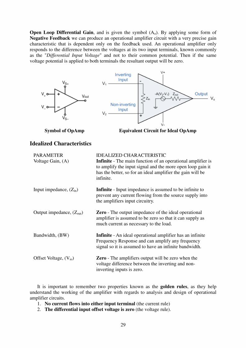
29
Open Loop Differential Gain, and is given the symbol (Ao). By applying some form of
Negative Feedback we can produce an operational amplifier circuit with a very precise gain
characteristic that is dependent only on the feedback used. An operational amplifier only
responds to the difference between the voltages at its two input terminals, known commonly
as the "Differential Input Voltage" and not to their common potential. Then if the same
voltage potential is applied to both terminals the resultant output will be zero.
Symbol of OpAmp Equivalent Circuit for Ideal OpAmp
Idealized Characteristics
PARAMETER IDEALIZED CHARACTERISTIC
Voltage Gain, (A) Infinite - The main function of an operational amplifier is
to amplify the input signal and the more open loop gain it
has the better, so for an ideal amplifier the gain will be
infinite.
Input impedance, (Zin) Infinite - Input impedance is assumed to be infinite to
prevent any current flowing from the source supply into
the amplifiers input circuitry.
Output impedance, (Zout) Zero - The output impedance of the ideal operational
amplifier is assumed to be zero so that it can supply as
much current as necessary to the load.
Bandwidth, (BW) Infinite - An ideal operational amplifier has an infinite
Frequency Response and can amplify any frequency
signal so it is assumed to have an infinite bandwidth.
Offset Voltage, (Vio) Zero - The amplifiers output will be zero when the
voltage difference between the inverting and non-
inverting inputs is zero.
It is important to remember two properties known as the golden rules, as they help
understand the working of the amplifier with regards to analysis and design of operational
amplifier circuits.
1. No current flows into either input terminal (the current rule)
2. The differential input offset voltage is zero (the voltage rule).

30
However, real Operational Amplifiers (e.g. 741) do not have infinite gain or
bandwidth but have a typical "Open Loop Gain" which is defined as the amplifiers output
amplification without any external feedback signals connected to it and for a typical
operational amplifier is about 100dB at DC (zero Hz). This output gain decreases linearly
with frequency down to "Unity Gain" or 1, at about 1MHz and this is shown in the following
open loop gain response curve. From this frequency response curve we can see that the
product of the gain against frequency is constant at any point along the curve. Also that the
unity gain (0dB) frequency also determines the gain of the amplifier at any point along the
curve. This constant is generally known as the Gain Bandwidth Product or GBP.
Therefore, GBP = Gain × Bandwidth or A × BW.
Open-loop Frequency Response Curve
For example, from the graph above the gain of the amplifier at 100kHz = 20dB or 10, then
the
GBP = 100,000Hz x 10 = 1,000,000.
Similarly, a gain at 1kHz = 60dB or 1000, therefore the
GBP = 1,000 x 1,000 = 1,000,000. The same!.
The Voltage Gain (A) of the amplifier can be found using the following formula:
i
o
V
VAGain ====,
and in Decibels or (dB) is given as:
i
o
V
VA log20log20 ====

31
Bandwidth of Operational Amplifier
The operational amplifiers bandwidth is the frequency range over which the voltage
gain of the amplifier is above 70.7% or -3dB (where 0dB is the maximum) of its maximum
output value as shown below.
Here we have used the 40dB line as an example. The -3dB or 70.7% of Vmax down
point from the frequency response curve is given as 37dB. Taking a line across until it
intersects with the main GBP curve gives us a frequency point just above the 10kHz line at
about 12 to 15kHz. We can now calculate this more accurately as we already know the GBP
of the amplifier, in this particular case 1MHz.
Example No1.
Using the formula 20 log (A), we can calculate the bandwidth of the amplifier as:
37 = 20 log A therefore, A = anti-log (37 ÷ 20) = 70.8
GBP ÷ A = Bandwidth, therefore, 1,000,000 ÷ 70.8 = 14.124Hz, or 14kHz
Then the bandwidth of the amplifier at a gain of 40dB is given as 14kHz as predicted from
the graph.
Example No2.
If the gain of the operational amplifier was reduced by half to say 20dB in the above
frequency response curve, the -3dB point would now be at 17dB. This would then give us an
overall gain of 7.08, therefore A = 7.08. If we use the same formula as above this new gain
would give us a bandwidth of 141.2kHz, ten times more than at 40dB.
It can therefore be seen that by reducing the overall open loop gain of an operational
amplifier its bandwidth is increased and vice versa. The -3dB point is also known as the "half
power point", as the output power of the amplifier is at half its maximum value at this point.
Op-amp types
Operational amplifiers can be connected using external resistors or capacitors in a
number of different ways to form basic "Building Block" circuits such as, Inverting, Non-
32
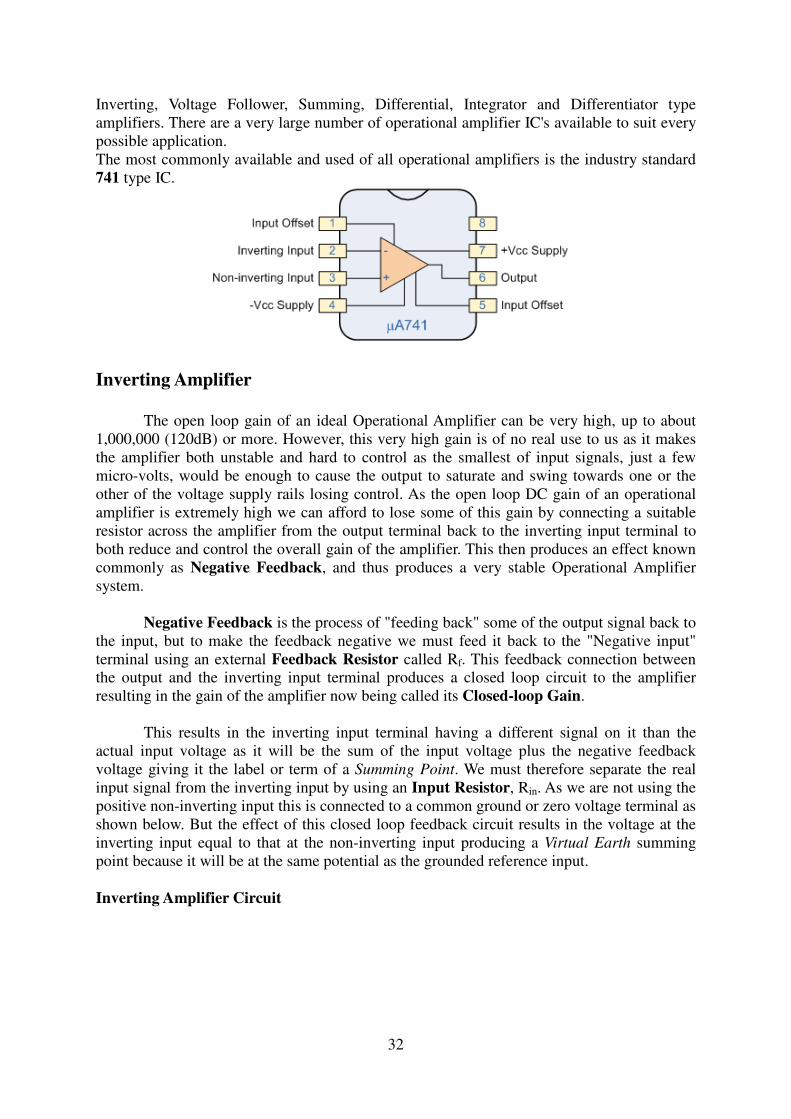
Inverting, Voltage Follower, Summing, Differential, Integrator and Differentiator type
amplifiers. There are a very large number of operational amplifier IC's available to suit every
possible application.
The most commonly available and used of all operational amplifiers is the industry standard
741 type IC.
Inverting Amplifier
The open loop gain of an ideal Operational Amplifier can be very high, up to about
1,000,000 (120dB) or more. However, this very high gain is of no real use to us as it makes
the amplifier both unstable and hard to control as the smallest of input signals, just a few
micro-volts, would be enough to cause the output to saturate and swing towards one or the
other of the voltage supply rails losing control. As the open loop DC gain of an operational
amplifier is extremely high we can afford to lose some of this gain by connecting a suitable
resistor across the amplifier from the output terminal back to the inverting input terminal to
both reduce and control the overall gain of the amplifier. This then produces an effect known
commonly as Negative Feedback, and thus produces a very stable Operational Amplifier
system.
Negative Feedback is the process of "feeding back" some of the output signal back to
the input, but to make the feedback negative we must feed it back to the "Negative input"
terminal using an external Feedback Resistor called Rf. This feedback connection between
the output and the inverting input terminal produces a closed loop circuit to the amplifier
resulting in the gain of the amplifier now being called its Closed-loop Gain.
This results in the inverting input terminal having a different signal on it than the
actual input voltage as it will be the sum of the input voltage plus the negative feedback
voltage giving it the label or term of a Summing Point. We must therefore separate the real
input signal from the inverting input by using an Input Resistor, Rin. As we are not using the
positive non-inverting input this is connected to a common ground or zero voltage terminal as
shown below. But the effect of this closed loop feedback circuit results in the voltage at the
inverting input equal to that at the non-inverting input producing a Virtual Earth summing
point because it will be at the same potential as the grounded reference input.
Inverting Amplifier Circuit
33
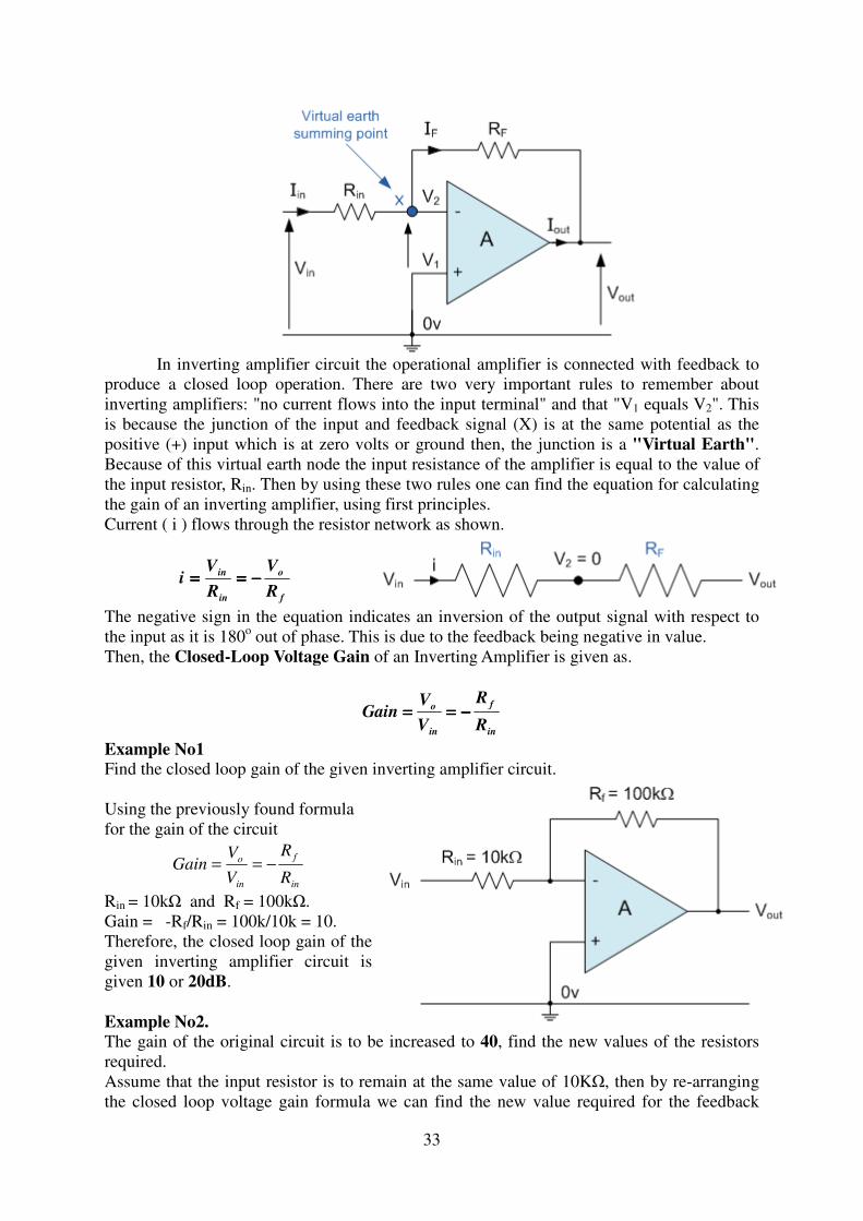
In inverting amplifier circuit the operational amplifier is connected with feedback to
produce a closed loop operation. There are two very important rules to remember about
inverting amplifiers: "no current flows into the input terminal" and that "V1 equals V2". This
is because the junction of the input and feedback signal (X) is at the same potential as the
positive (+) input which is at zero volts or ground then, the junction is a "Virtual Earth".
Because of this virtual earth node the input resistance of the amplifier is equal to the value of
the input resistor, Rin. Then by using these two rules one can find the equation for calculating
the gain of an inverting amplifier, using first principles.
Current ( i ) flows through the resistor network as shown.
f
o
in
in
R
V
R
Vi −−−−========
The negative sign in the equation indicates an inversion of the output signal with respect to
the input as it is 180o out of phase. This is due to the feedback being negative in value.
Then, the Closed-Loop Voltage Gain of an Inverting Amplifier is given as.
in
f
in
o
R
R
V
VGain −−−−========
Example No1
Find the closed loop gain of the given inverting amplifier circuit.
Using the previously found formula
for the gain of the circuit
in
f
in
o
R
R
V
VGain −==
Rin = 10kΩ and Rf = 100kΩ.
Gain = -Rf/Rin = 100k/10k = 10.
Therefore, the closed loop gain of the
given inverting amplifier circuit is
given 10 or 20dB.
Example No2.
The gain of the original circuit is to be increased to 40, find the new values of the resistors
required.
Assume that the input resistor is to remain at the same value of 10KΩ, then by re-arranging
the closed loop voltage gain formula we can find the new value required for the feedback

34
resistor Rf.
Gain = -Rf/Rin
So, Rf = Gain x Rin
Rf = 400,000 or 400KΩ
The new values of resistors required for the circuit to have a gain of 40 would be,
Rin = 10KΩ and Rf = 400KΩ.
The formula could also be rearranged to give a new value of Rin, keeping the same value of
Rf.
Unity Gain Inverter One final point to note about Inverting Amplifiers, if the two resistors are of equal value, Rin
= Rf then the gain of the amplifier will be -1 producing a complementary form of the input
voltage at its output as Vout = -Vin. This type of inverting amplifier configuration is generally
called a Unity Gain Inverter of simply an Inverting Buffer.
Non-inverting Amplifier
The second basic configuration of an operational amplifier circuit is that of a Non-
inverting Amplifier. In this configuration, the input voltage signal, (Vin) is applied directly
to the Non-inverting (+) input terminal which means that the output gain of the amplifier
becomes "Positive" in value in contrast to the "Inverting Amplifier" circuit whose output gain
is negative in value. Feedback control of the non-inverting amplifier is achieved by applying
a small part of the output voltage signal back to the inverting (-) input terminal via a Rf - R2
voltage divider network, again producing negative feedback. This produces a Non-inverting
Amplifier circuit with very good stability, a very high input impedance, Rin approaching
infinity (as no current flows into the positive input terminal) and a low output impedance, rout
as shown below.
Non-inverting Amplifier Circuit
Since no current flows into the input of the amplifier, V1 = Vin. In other words the
junction is a "Virtual Earth" summing point. Because of this virtual earth node, the resistors
Rf and R2 form a simple voltage divider network across the amplifier and the voltage gain of
the circuit is determined by the ratios of R2 and Rf as shown below.
Equivalent Voltage Divider Network
Then using the formula to calculate the output voltage of a
potential divider network, we can calculate the output Voltage

35
Gain of the Non-inverting Amplifier as:
)1(2
0R
RVV
f
in +=
2
1R
R
V
VGain
f
in
o ++++========
We can see that the overall gain of a Non-Inverting Amplifier is greater but never less than 1,
is positive and is determined by the ratio of the values of Rf and R2. If the feedback resistor Rf
is zero the gain will be equal to 1, and if resistor R2 is zero the gain will approach infinity, but
in practice it will be limited to the operational amplifiers open-loop differential gain, (Ao).
Voltage Follower (Unity Gain Buffer)
If we made the feedback resistor, Rf = 0 then the circuit will have a fixed gain of "1"
and would be classed as a Voltage Follower. As the input signal is connected directly to the
non-inverting input of the amplifier the output signal is not inverted resulting in the output
voltage being equal to the input voltage, Vout = Vin. This then makes the Voltage Follower
circuit ideal as a Unity Gain Buffer circuit because of its isolation properties as impedance or
circuit isolation is more important than amplification. The input impedance of the voltage
follower circuit is very high, typically above 1MΩ.
In this circuit, Rin has increased to infinity and Rf reduced to zero, the feedback is
100% and Vout is exactly equal to Vin giving it a fixed gain of 1 or unity. As the input voltage
Vin is applied to the non-inverting input the gain of the amplifier is given as:
1
)(
========
========
−−−−====
−−−−++++
in
o
oin
oino
V
VGain
VVVV
VVAV
The voltage follower or unity gain buffer is a special and very useful type of Non-
inverting amplifier circuit that is commonly used in electronics to isolate circuits from each
other especially in High-order state variable or Sallen-Key type active filters to separate one
filter stage from the other. Typical digital buffer IC's available are the 74LS125 Quad 3-state
buffer or the more common 74LS244 Octal buffer.
One final thought, the output voltage gain of the voltage follower circuit with closed
loop gain is Unity, the voltage gain of an ideal operational amplifier with open loop gain (no
feedback) is infinite. Then by carefully selecting the feedback components we can control the
amount of gain produced by an Operational Amplifier anywhere from 1 to infinity.
Summing Amplifier

36
The Summing Amplifier is a very flexible circuit based upon the standard Inverting
Operational Amplifier configuration. We saw previously that the inverting amplifier has a
single input signal applied to the inverting input terminal. If we add another input resistor
equal in value to the original input resistor, Rin we end up with another operational amplifier
circuit called a Summing Amplifier, "Summing Inverter" or even a "Voltage Adder" circuit
as shown below
Summing Amplifier Circuit
The output voltage, (Vout) now becomes proportional to the sum of the input voltages, V1, V2,
V3 etc. Then we can modify the original equation for the inverting amplifier to take account
of these new inputs thus:
(((( ))))321
321
321
, VVVR
RVthen
R
V
R
V
R
VIIII
in
F
out
ininin
F
++++++++−−−−====
++++++++−−−−====++++++++====
The Summing Amplifier is a very flexible circuit indeed, enabling us to effectively
"Add" or "Sum" together several individual input signals. If the input resistors are all equal a
unity gain inverting adder can be made. However, if the input resistors are of different values
a "scaling summing amplifier" is produced which gives a weighted sum of the input signals.
Example No1
Find the output voltage of the following Summing Amplifier circuit.
The gain of the circuit
in
f
in
o
R
R
V
VGain −−−−========
substituting the values of the resistors,
52
102,10
1
101 −−−−====
ΩΩΩΩ
ΩΩΩΩ====−−−−====
ΩΩΩΩ
ΩΩΩΩ====
k
kA
k
kA
The output voltage is the sum of the
two amplified input signals:
mV
mVmVV o
45
))5(5())2(10(
−−−−====
−−−−++++−−−−====
37
If the input resistances of a summing amplifier are connected to potentiometers the individual
input signals can be mixed together by varying amounts. For example, for measuring
temperature, you could add a negative offset voltage to make the display read "0" at the
freezing point or produce an audio mixer for adding or mixing together individual waveforms
(sounds) from different source channels (vocals, instruments, etc) before sending them
combined to an audio amplifier.
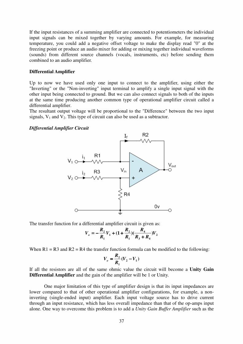
Differential Amplifier
Up to now we have used only one input to connect to the amplifier, using either the
"Inverting" or the "Non-inverting" input terminal to amplify a single input signal with the
other input being connected to ground. But we can also connect signals to both of the inputs
at the same time producing another common type of operational amplifier circuit called a
differential amplifier.
The resultant output voltage will be proportional to the "Difference" between the two input
signals, V1 and V2. This type of circuit can also be used as a subtractor.
Differential Amplifier Circuit
The transfer function for a differential amplifier circuit is given as:
2
43
4
1
2
1
1
2 ))(1( VRR
R
R
RV
R
RVo
++++++++++++−−−−====
When R1 = R3 and R2 = R4 the transfer function formula can be modified to the following:
)( 12
1
2 VVR
RVo −−−−====
If all the resistors are all of the same ohmic value the circuit will become a Unity Gain
Differential Amplifier and the gain of the amplifier will be 1 or Unity.
One major limitation of this type of amplifier design is that its input impedances are
lower compared to that of other operational amplifier configurations, for example, a non-
inverting (single-ended input) amplifier. Each input voltage source has to drive current
through an input resistance, which has less overall impedance than that of the op-amps input
alone. One way to overcome this problem is to add a Unity Gain Buffer Amplifier such as the
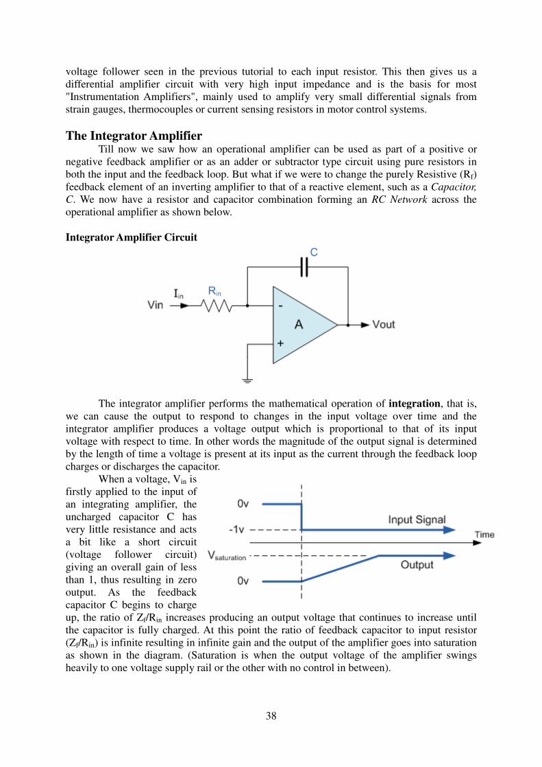
38
voltage follower seen in the previous tutorial to each input resistor. This then gives us a
differential amplifier circuit with very high input impedance and is the basis for most
"Instrumentation Amplifiers", mainly used to amplify very small differential signals from
strain gauges, thermocouples or current sensing resistors in motor control systems.
The Integrator Amplifier Till now we saw how an operational amplifier can be used as part of a positive or
negative feedback amplifier or as an adder or subtractor type circuit using pure resistors in
both the input and the feedback loop. But what if we were to change the purely Resistive (Rf)
feedback element of an inverting amplifier to that of a reactive element, such as a Capacitor,
C. We now have a resistor and capacitor combination forming an RC Network across the
operational amplifier as shown below.
Integrator Amplifier Circuit
The integrator amplifier performs the mathematical operation of integration, that is,
we can cause the output to respond to changes in the input voltage over time and the
integrator amplifier produces a voltage output which is proportional to that of its input
voltage with respect to time. In other words the magnitude of the output signal is determined
by the length of time a voltage is present at its input as the current through the feedback loop
charges or discharges the capacitor.
When a voltage, Vin is
firstly applied to the input of
an integrating amplifier, the
uncharged capacitor C has
very little resistance and acts
a bit like a short circuit
(voltage follower circuit)
giving an overall gain of less
than 1, thus resulting in zero
output. As the feedback
capacitor C begins to charge
up, the ratio of Zf/Rin increases producing an output voltage that continues to increase until
the capacitor is fully charged. At this point the ratio of feedback capacitor to input resistor
(Zf/Rin) is infinite resulting in infinite gain and the output of the amplifier goes into saturation
as shown in the diagram. (Saturation is when the output voltage of the amplifier swings
heavily to one voltage supply rail or the other with no control in between).
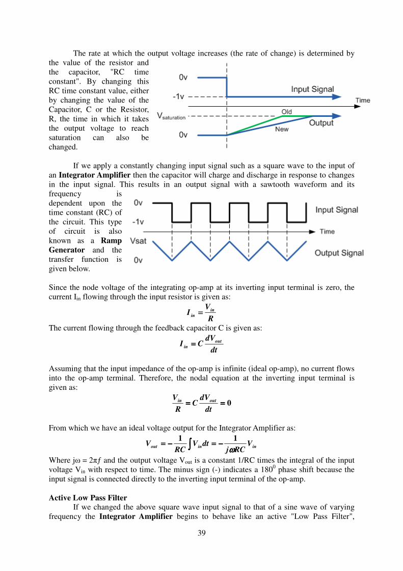
39
The rate at which the output voltage increases (the rate of change) is determined by
the value of the resistor and
the capacitor, "RC time
constant". By changing this
RC time constant value, either
by changing the value of the
Capacitor, C or the Resistor,
R, the time in which it takes
the output voltage to reach
saturation can also be
changed.
If we apply a constantly changing input signal such as a square wave to the input of
an Integrator Amplifier then the capacitor will charge and discharge in response to changes
in the input signal. This results in an output signal with a sawtooth waveform and its
frequency is
dependent upon the
time constant (RC) of
the circuit. This type
of circuit is also
known as a Ramp
Generator and the
transfer function is
given below.
Since the node voltage of the integrating op-amp at its inverting input terminal is zero, the
current Iin flowing through the input resistor is given as:
R
VI in
in ====
The current flowing through the feedback capacitor C is given as:
dt
dVCI out
in ====
Assuming that the input impedance of the op-amp is infinite (ideal op-amp), no current flows
into the op-amp terminal. Therefore, the nodal equation at the inverting input terminal is
given as:
0========dt
dVC
R
V outin
From which we have an ideal voltage output for the Integrator Amplifier as:
ininout VRCj
dtVRC
Vωωωω
11−−−−====−−−−==== ∫∫∫∫
Where jω = 2πƒ and the output voltage Vout is a constant 1/RC times the integral of the input
voltage Vin with respect to time. The minus sign (-) indicates a 1800 phase shift because the
input signal is connected directly to the inverting input terminal of the op-amp.
Active Low Pass Filter
If we changed the above square wave input signal to that of a sine wave of varying
frequency the Integrator Amplifier begins to behave like an active "Low Pass Filter",
40
passing low frequency signals while attenuating the high frequencies. However, at DC (0Hz)
the capacitor acts like an open circuit blocking any feedback voltage resulting in zero
negative feedback from the output back to the input of the amplifier. Then the amplifier
effectively is connected as a normal open-loop amplifier with very high open-loop gain
resulting in the output voltage saturating.
The addition of a large value resistor, R2 across the capacitor, C gives the circuit the
characteristics of an inverting amplifier with finite closed-loop gain of R2/Rin at very low
frequencies while acting as an integrator at higher frequencies. This then forms the basis of
an Active Low Pass Filter.
The AC Integrator with DC Gain Control
The Differentiator Amplifier
The basic differentiator amplifier circuit is the exact opposite to that of the Integrator
operational amplifier circuit. Here, the position of the capacitor and resistor have been
reversed and now the Capacitor, C is connected to the input terminal of the inverting
amplifier while the Resistor, Rf forms the negative feedback element across the operational
amplifier. This circuit performs the mathematical operation of Differentiation, i.e. it
produces a voltage output which is proportional to rate-of-change of the input voltage and
the current flowing through the capacitor. In other words the faster or larger the change to the
input voltage signal, the greater the input current, the greater will be the output voltage
change in response becoming more of a "spike" in shape.
As with the integrator circuit, we have a resistor and capacitor forming an RC
Network across the operational amplifier and the reactance (Xc) of the capacitor plays a
major role in the performance of a differentiator amplifier.
Differentiator Amplifier Circuit
41
Since the node voltage of the operational amplifier at its inverting input terminal is zero, the
current, i flowing through the capacitor will be given as:
F
o
FFINR
VIIi −== and
The Charge on the Capacitor = Capacitance x Voltage across the Capacitor
INVCQ ×=
The rate of change of this charge is
dt
dVC
dt
dQ IN=
but dQ/dt is the capacitor current i
F
IN
IN Idt
dVCi ==
From which we have an ideal voltage output for the Differentiator Amplifier is given as:
dt
dVCRV IN
FO −=
Therefore, the output voltage Vout is a constant -Rf.C times the derivative of the input voltage
Vin with respect to time. The minus sign indicates a 1800 phase shift because the input signal
is connected to the inverting input terminal of the operational amplifier.
Active High Pass Filter
The capacitor blocks any DC content only allowing AC type signals whose frequency
is dependent on the rate of change of the input signal, to pass through. At low frequencies the
reactance of the capacitor is "High" resulting in a low gain (Rf/Xc) and low output voltage
from the op-amp. At higher frequencies the reactance of the capacitor is much lower resulting
in a higher gain and higher output voltage from the differentiator amplifier. Thus with
sinusoidal wave at the input this circuit will act as an active high pass filter circuit.
The basic single resistor and single capacitor differentiator circuit is not widely used
to reform the mathematical function of differentiation because of the two inherent faults
mentioned above: Instability and Noise.
At high frequencies a differentiator circuit becomes unstable and will start to oscillate. To
avoid this, the high frequency gain of the circuit needs to be reduced by adding an additional
small value capacitor, Cf, across the feedback resistor Rf. Also, the capacitive input makes it
very susceptible to random noise signals and any noise or harmonics present in the circuit
will be amplified more than the input signal itself. This is because the output is proportional
to the slope of the input voltage. So some means of limiting the bandwidth in order to achieve
closed-loop stability is required. In order to reduce the overall closed-loop gain of the circuit
at high frequencies, an extra Resistor, Rin is added to the input as shown below. Thus, the new
circuit acts like a Differentiator amplifier at low frequencies and an amplifier with resistive
feedback at high frequencies giving much better noise rejection.

42
Differentiator Waveforms
If we apply a constantly changing signal such as a Square-wave, Triangular or Sine-wave
type signal to the input of a differentiator amplifier circuit the resultant output signal will be
changed and whose final shape is dependent upon the RC time constant of the
Resistor/Capacitor combination.

43
Study of Basic OPAMP configurations
Objectives:
(I) Study of the inverting amplifier configuration and to find its gain
(II) Study of the non-inverting amplifier configuration and to find its gain
Apparatus:
1. OPAMP IC 741
2. Resistors: 1K (2 nos), 10K, 50K
3. D.C. power supply
4. Digital multimeter
5. Bread board
6. Connecting wires
Theory:
Please refer the supplementary note.
Circuit Diagram:
Inverting amplifier
44
Non-inverting amplifier
Procedure:
(I) Inverting amplifier
1. Configure the circuit as shown in the circuit diagram. Connect the pins 7 and 4 of the
IC to the ±15V output terminals of the D.C. power supply. Connect the 0V terminal to
ground. Choose Rin = 1K and Rf = 10K. Measure the resistance values with
multimeter and calculate gain, -(Rf/Rin). Connect a resistor R3 (= RinRf ≈ Rin) as
shown in the circuit diagram so as to minimize offset due to input bias current.
2. Connect one of the output terminals of the D.C. power supply (0-30V) at the
inverting input (pin no. 2).
3. Switch on the power supply and apply different voltages in the range 0- 1.5V (why?)
in steps of 0.2 V at the inverting terminal. Measure this input using a digital
multimeter.
4. Measure the corresponding output voltages with the multimeter and calculate gain
Vo/Vin. Note the sign of the output voltage.
5. Now, replace Rf by 50K. Measure the resistance value with multimeter and calculate
gain, -(Rf/Rin).
6. Apply different voltages in the range 0- 0.5V in steps of 0.1 V at the inverting
terminal. Measure this input using a digital multimeter.
7. Measure the corresponding output voltages with the multimeter and calculate gain
Vo/Vin.
8. Plot graphs for V in ~ Vo for both the values of RF.
9. You may also use a function generator to give a sinusoidal input and notice the output
waveform using an oscilloscope.
(II) Non-inverting amplifier
1. Configure the circuit as shown in the circuit diagram with Rin = 1K and Rf = 10K.
using the measured value of resistance calculate gain, 1+ (Rf/Rin).
2. Connect one of the output terminals of the D.C. power supply (0-30V) at the non-
inverting input (pin no. 3).
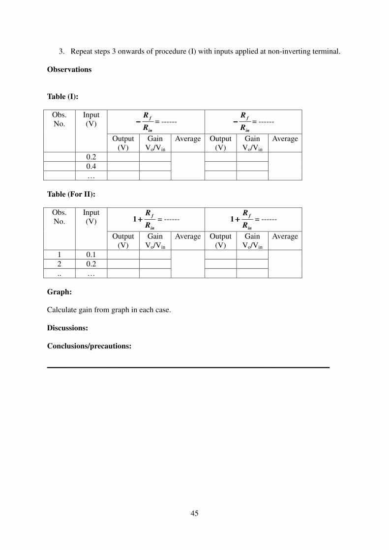
45
3. Repeat steps 3 onwards of procedure (I) with inputs applied at non-inverting terminal.
Observations
Table (I):
Obs.
No.
Input
(V) in
f
R
R−−−− = ------
in
f
R
R−−−− = ------
Output
(V)
Gain
Vo/Vin
Average Output
(V)
Gain
Vo/Vin
Average
0.2
0.4
…
Table (For II):
Obs.
No.
Input
(V) in
f
R
R++++1 = ------
in
f
R
R++++1 = ------
Output
(V)
Gain
Vo/Vin
Average Output
(V)
Gain
Vo/Vin
Average
1 0.1
2 0.2
.. …
Graph:
Calculate gain from graph in each case.
Discussions:
Conclusions/precautions:
________________________________________________________________________

46
Applications of OPAMP as Comparator and Schmitt Trigger
Objectives:
(i) Study of OPAMP as comparator
(ii) Study of OPAMP as Schmitt trigger
(i) Comparator
Theory
When the feedback signal (voltage) is applied to the inverting (-) input of the op-amp
then the feedback is negative. Negative feedback tends to reduce the difference between the
voltages at the inverting and non-inverting terminals and make linear circuits. Without
negative feedback the op-amp output is highly sensitive to the input, which can be used to
design switching or nonlinear circuits. The voltage comparator is a device which uses no
feedback; then saturation is the desired result. In this circuit we want a simple yes-no answer
to be signified by either positive saturation or negative saturation of the output.
In the circuit diagrams shown below, for Fig.(i), if Vin > 0, Vo ≈ V++ and if Vin < 0, Vo
≈ V--.The output is no longer linearly related to the input– it’s more like a digital signal, high
or low depending on how Vin compares to ground (0 V). Needless to mention that, if Vin is
applied at the inverting terminal with respect to a grounded non-inverting terminal, the output
will switch to low when Vin >0. Figure (ii) shows a small modification, allowing the circuit to
switch its output when Vin crosses a certain preset voltage level, often called the threshold
voltage, Vth.
Typical applications of this circuit are crossover detectors, analog to digital converters
or counting applications where one wants to count pulses that exceed a certain voltage level.
Components/Equipments:
(i) OPAMP (IC-741) chip, (ii) A D.C. power supply, (iii) A digital multimeter (DMM), (iv) A
digital storage oscilloscope (DSO), (v) Connecting wires, (vi) Breadboard
Circuit Diagram:
(i)
47
(ii)
Procedure:
1. Construct the comparator circuit on the breadboard as shown in the circuit diagram.
Take care to give proper connections at the desired pins of the IC.
2. Use terminal C of the d.c. power supply (denoted by V+ and V- knobs) to provide
power supply to IC. Connect the 0Vterminal to ground.
3. Connect terminal A of the d.c. power supply (0-30V) at the input. Use terminal B (5V)
to provide threshold voltage Vth for circuit shown in Fig. (ii).
4. Vary the input from a negative value to a positive value through 0.
5. Using the DMM, measure and tabulate Vin and Vout. You can also look at the output
using a DSO by coupling the output to it in DC mode.
6. Make a plot of Vout vs Vin for each circuit. Estimate Vth from graph for Fig. (ii) and
compare with the Vth value actually applied. You can repeat the same procedure for
different values of threshold.
7. Repeat the entire procedure described above with input at the inverting terminal and
the non-inverting terminal being grounded w/o and with the threshold voltage
connected to it.
Observations:
For Fig. (i)
Obs.No Vi
(V)
Vo
(V)
1
..
..
For Fig. (ii)
Vth = ----- V
Obs.No Vi
(V)
Vo
(V)
1
..
..
Discussions:
Precautions:
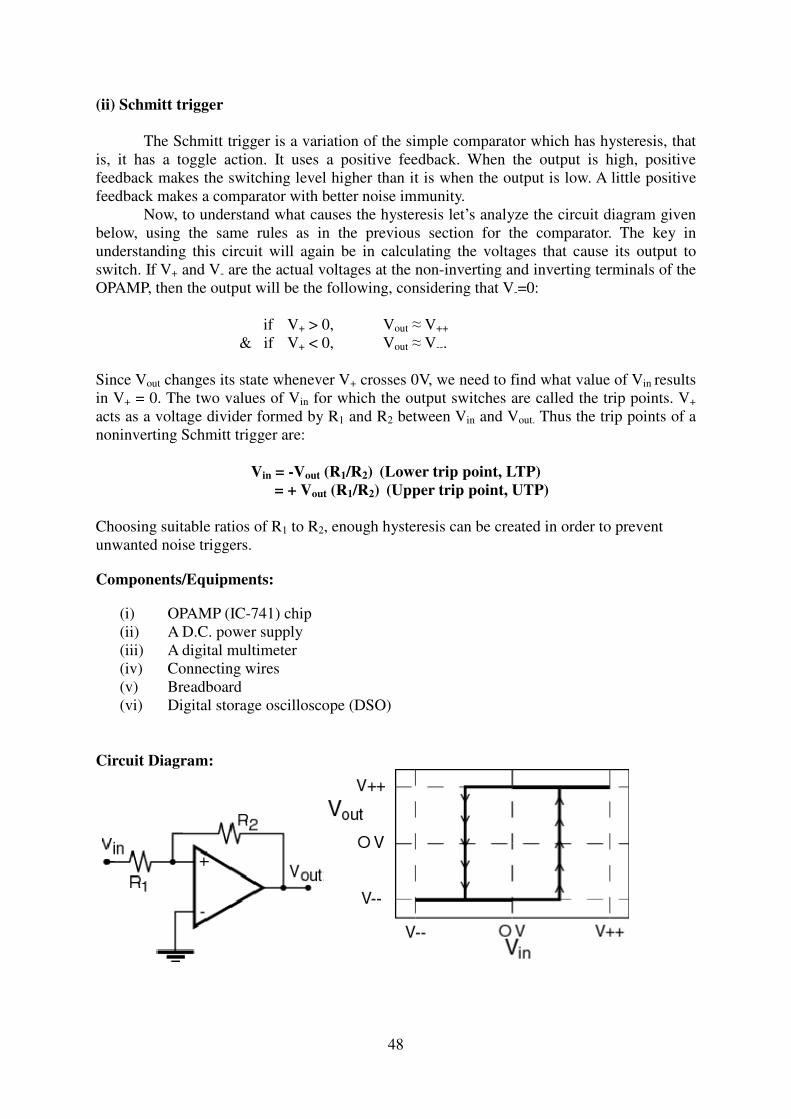
48
(ii) Schmitt trigger
The Schmitt trigger is a variation of the simple comparator which has hysteresis, that
is, it has a toggle action. It uses a positive feedback. When the output is high, positive
feedback makes the switching level higher than it is when the output is low. A little positive
feedback makes a comparator with better noise immunity.
Now, to understand what causes the hysteresis let’s analyze the circuit diagram given
below, using the same rules as in the previous section for the comparator. The key in
understanding this circuit will again be in calculating the voltages that cause its output to
switch. If V+ and V- are the actual voltages at the non-inverting and inverting terminals of the
OPAMP, then the output will be the following, considering that V-=0:
if V+ > 0, Vout ≈ V++
& if V+ < 0, Vout ≈ V--.
Since Vout changes its state whenever V+ crosses 0V, we need to find what value of Vin results
in V+ = 0. The two values of Vin for which the output switches are called the trip points. V+
acts as a voltage divider formed by R1 and R2 between Vin and Vout. Thus the trip points of a
noninverting Schmitt trigger are:
Vin = -Vout (R1/R2) (Lower trip point, LTP)
= + Vout (R1/R2) (Upper trip point, UTP)
Choosing suitable ratios of R1 to R2, enough hysteresis can be created in order to prevent
unwanted noise triggers.
Components/Equipments:
(i) OPAMP (IC-741) chip
(ii) A D.C. power supply
(iii) A digital multimeter
(iv) Connecting wires
(v) Breadboard
(vi) Digital storage oscilloscope (DSO)
Circuit Diagram:
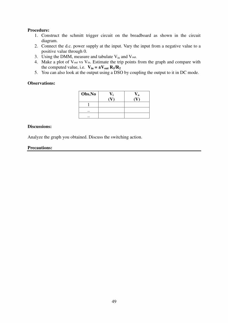
49
Procedure:
1. Construct the schmitt trigger circuit on the breadboard as shown in the circuit
diagram.
2. Connect the d.c. power supply at the input. Vary the input from a negative value to a
positive value through 0.
3. Using the DMM, measure and tabulate Vin and Vout.
4. Make a plot of Vout vs Vin. Estimate the trip points from the graph and compare with
the computed value, i.e. Vin = ±Vout R1/R2
5. You can also look at the output using a DSO by coupling the output to it in DC mode.
Observations:
Obs.No Vi
(V)
Vo
(V)
1
..
..
Discussions:
Analyze the graph you obtained. Discuss the switching action.
Precautions:
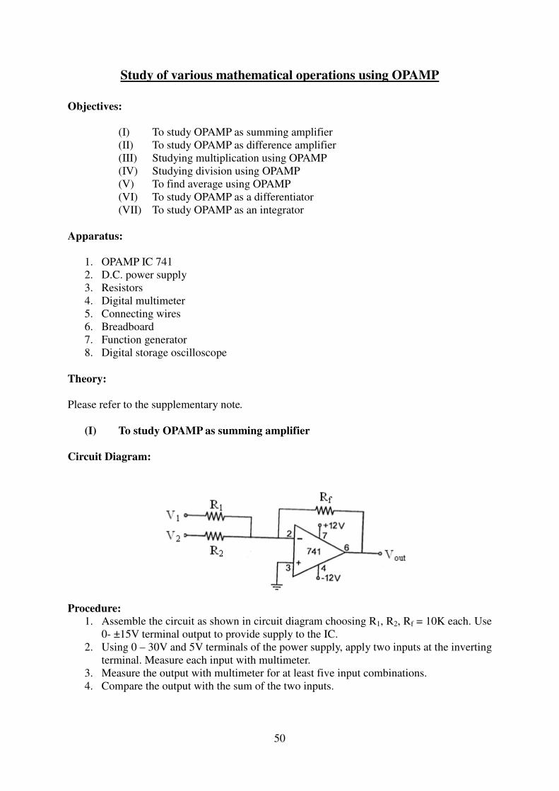
50
Study of various mathematical operations using OPAMP
Objectives:
(I) To study OPAMP as summing amplifier
(II) To study OPAMP as difference amplifier
(III) Studying multiplication using OPAMP
(IV) Studying division using OPAMP
(V) To find average using OPAMP
(VI) To study OPAMP as a differentiator
(VII) To study OPAMP as an integrator
Apparatus:
1. OPAMP IC 741
2. D.C. power supply
3. Resistors
4. Digital multimeter
5. Connecting wires
6. Breadboard
7. Function generator
8. Digital storage oscilloscope
Theory:
Please refer to the supplementary note.
(I) To study OPAMP as summing amplifier
Circuit Diagram:
Procedure:
1. Assemble the circuit as shown in circuit diagram choosing R1, R2, Rf = 10K each. Use
0- ±15V terminal output to provide supply to the IC.
2. Using 0 – 30V and 5V terminals of the power supply, apply two inputs at the inverting
terminal. Measure each input with multimeter.
3. Measure the output with multimeter for at least five input combinations.
4. Compare the output with the sum of the two inputs.
51
Observations:
Obs.No V1
(V)
V2
(V)
Vout
(V)
V1 + V2
(V)
1
..
5
Disscusions:
(II) To study OPAMP as difference amplifier
Circuit Diagram:
Procedure:
1. Assemble the circuit as shown in circuit diagram choosing R1, R2, R3, Rf = 10K each.
Use 0- ±15V terminal output to provide supply to the IC.
2. Using 0 – 30V and 5V terminals of the power supply, apply two inputs, one at the
inverting and the other at the non-inverting terminal. Measure each input with
multimeter.
3. Measure output with multimeter for at least five input combinations.
4. Compare the output with the difference of the two inputs.
Observations:
Obs.No V1
(V)
V2
(V)
Vout
(V)
V2 – V1
(V)
1
..
5
Disscusions:
(III) Studying multiplication using OPAMP
Circuit Diagram:
52
Procedure:
1. Assemble the circuit as shown in circuit diagram choosing R1, R2 = 1K each and Rf =
10K. Use 0- ±15V terminal output to provide supply to the IC.
2. Using 0 – 30V terminal of the power supply, apply different input values at the
inverting terminal. Measure each input with multimeter.
3. Measure output with multimeter for at least five different input values.
4. Compare the measured output with the calculated one.
Observations:
Obs.No V1
(V)
Vout (Measured)
(V)
Vout (Calculated)
(V)
1
..
..
Discussions:
(IV) Studying division using OPAMP
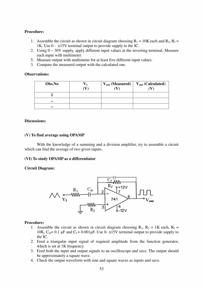
53
Procedure:
1. Assemble the circuit as shown in circuit diagram choosing R1 = 10K each and R2, Rf =
1K. Use 0 - ±15V terminal output to provide supply to the IC.
2. Using 0 – 30V supply, apply different input values at the inverting terminal. Measure
each input with multimeter.
5. Measure output with multimeter for at least five different input values.
3. Compare the measured output with the calculated one.
Observations:
Obs.No V1
(V)
Vout (Measured)
(V)
Vout (Calculated)
(V)
1
..
..
Discussions:
(V) To find average using OPAMP
With the knowledge of a summing and a division amplifier, try to assemble a circuit
which can find the average of two given inputs.
(VI) To study OPAMP as a differentiator
Circuit Diagram:
Procedure:
1. Assemble the circuit as shown in circuit diagram choosing R1, R2 = 1K each, Rf =
10K, Cin= 0.1 μF and Cf = 0.001μF. Use 0- ±15V terminal output to provide supply to
the IC.
2. Feed a triangular input signal of required amplitude from the function generator,
which is set at 1K frequency.
3. Feed both the input and output signals to an oscilloscope and save. The output should
be approximately a square wave.
4. Check the output waveform with sine and square waves as inputs and save.
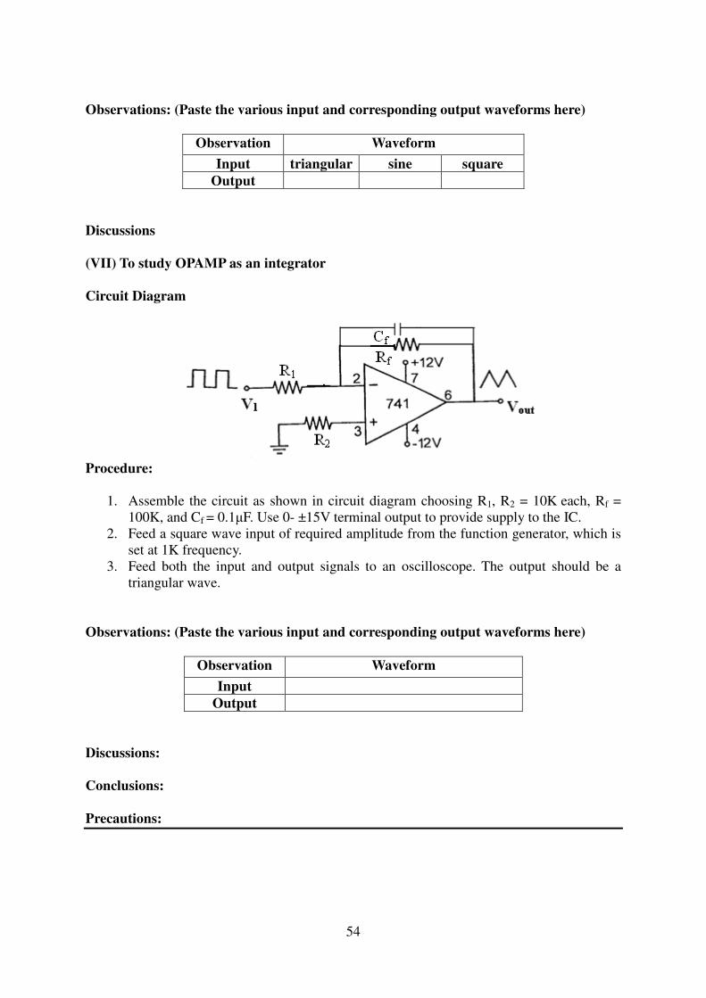
54
Observations: (Paste the various input and corresponding output waveforms here)
Observation Waveform
Input triangular sine square
Output
Discussions
(VII) To study OPAMP as an integrator
Circuit Diagram
Procedure:
1. Assemble the circuit as shown in circuit diagram choosing R1, R2 = 10K each, Rf =
100K, and Cf = 0.1μF. Use 0- ±15V terminal output to provide supply to the IC.
2. Feed a square wave input of required amplitude from the function generator, which is
set at 1K frequency.
3. Feed both the input and output signals to an oscilloscope. The output should be a
triangular wave.
Observations: (Paste the various input and corresponding output waveforms here)
Observation Waveform
Input
Output
Discussions:
Conclusions:
Precautions:

55
Phase Shift Oscillator using Opamps
Objectives:
To construct and determine the resonant frequency of
(i) A phase shift oscillator
Overview:
The main principle of oscillator is positive feedback. Block diagram of oscillator is
shown in Figure 1.
Figure.1
In the block diagram (Fig.1), Vd = Vf + Vin
Vo=AvVd and Vf = βVo
Using these relationships, following equation can be obtained:
=
.
When AVβ = 1, = ∞ =
, This will happen only when Vi n= 0. That is we get a signal at
output without any input. The condition AVβ = 1 is known as Barkhausen condition. This
condition expressed in polar form as follows. AVβ = 1 ∠0° 360°
Barkhausen condition gives two requirements for oscillation.
1) The magnitude of the loop gain must be equal to 1.
2) The total phase shift of the loop gain must be equal to 0° 360°.
Σ Amplifier
Av
Feedback
Circuit β
Vo output Vin=0 Vd
Vf

Phase shift Oscillator: Figure.2 gives the circuit diagram for a phase shift oscillator, which
consists of an op-amp as the amplifying stage and three RC cascaded networks as the
feedback circuit. The opamp used i
phase shifted. To feedback the output to input, additional 180° degree phase shift is achieved
by RC network.
Figure.2
The frequency of oscillation is given by,
at least 29. That is
= 29.
Feedback circuit with RC network gives 180 degree phase shift but decreases the output voltage by a factor of 29. That is
should be at least 29.
Procedure: Choose Rf = 100 K
shift oscillator. Determine the oscillating frequency using oscilloscope and compare with
calculated oscillation frequency.
Experimentally determine the minimum
the gain in the circuit. Obtain Lissajous figure (circle) with X
and estimate oscillating frequency. Try to make the circuit for some other oscillating
frequency by choosing compon
References: 1) OPAMPS and linear integrated circuits
2) http://textofvideo.nptel.iitm.ac.in/122106025/lec35.pdf
56
Figure.2 gives the circuit diagram for a phase shift oscillator, which
amp as the amplifying stage and three RC cascaded networks as the
feedback circuit. The opamp used in this oscillator is in the inverting mode, output is 180° is
phase shifted. To feedback the output to input, additional 180° degree phase shift is achieved
The frequency of oscillation is given by, = √!" and at this frequency gain must be
.
Feedback circuit with RC network gives 180 degree phase shift but decreases the output voltage by a factor of 29. That is β=1/29. For the oscillations AVβ = 1. Therefore, gain
= 100 KΩ, R = 2 KΩ, C = 0.1 uF, R=1 KΩ and construct a phase
Determine the oscillating frequency using oscilloscope and compare with
calculated oscillation frequency.
Experimentally determine the minimum gain required to sustain oscillations by varying
the gain in the circuit. Obtain Lissajous figure (circle) with X-Y mode of the oscilloscope
and estimate oscillating frequency. Try to make the circuit for some other oscillating
frequency by choosing components appropriately.
References: 1) OPAMPS and linear integrated circuits –Ramakant Gaykwad
http://textofvideo.nptel.iitm.ac.in/122106025/lec35.pdf
Figure.2 gives the circuit diagram for a phase shift oscillator, which
amp as the amplifying stage and three RC cascaded networks as the
n this oscillator is in the inverting mode, output is 180° is
phase shifted. To feedback the output to input, additional 180° degree phase shift is achieved
and at this frequency gain must be
Feedback circuit with RC network gives 180 degree phase shift but decreases the output = 1. Therefore, gain
and construct a phase
Determine the oscillating frequency using oscilloscope and compare with
gain required to sustain oscillations by varying
Y mode of the oscilloscope
and estimate oscillating frequency. Try to make the circuit for some other oscillating
Ramakant Gaykwad

57
Pass
Band Stop
Band
|H(jω)|
ωc ω
Fig. 1: LPF
PASSIVE (RC) FILTER CIRCUIT
OBJECTIVES:
(I) Study the transfer function and phase shift of a low pass RC filter network.
(II) Study the transfer function and phase shift of a high pass RC filter network.
OVERVIEW:
Filter circuits are used in a wide variety of applications. In the field of
telecommunication, band-pass filters are used in the audio frequency range (20 Hz to 20 kHz)
for modems and speech processing. High-frequency band-pass filters (several hundred MHz)
are used for channel selection in telephone central offices. Data acquisition systems usually
require anti-aliasing low-pass filters as well as low-pass noise filters in their preceding signal
conditioning stages. System power supplies often use band-rejection filters to suppress the
50-Hz line frequency and high frequency transients.
Frequency-selective or filter circuits pass only
those input signals to the output that are in a desired
range of frequencies (called pass band). The amplitude
of signals outside this range of frequencies (called stop
band) is reduced (ideally reduced to zero). The frequency
between pass and stop bands is called the cut-off
frequency (ωc). Typically in these circuits, the input and
output currents are kept to a small value and as such, the
current transfer function is not an important parameter.
The main parameter is the voltage transfer function in
the frequency domain, Hv(jω) = Vo/Vi. Subscript v of
Hv is frequently dropped. As H(jω) is complex number,
it has both a magnitude and a phase, filters in general introduce a phase difference between
input and output signals.
LOW AND HIGH-PASS FILTERS
A low pass filter or LPF attenuates or rejects all
high frequency signals and passes only low frequency
signals below its characteristic frequency called as cut-off
frequency, ωc. An ideal low-pass fillter's transfer function
is shown in Fig. 1. A high pass filter or HPF, is the exact
opposite of the LPF circuit. It attenuates or rejects all low
frequency signals and passes only high frequency signals
above ωc.
In practical filters, pass and stop bands are not clearly
defined, |H(jω)| varies continuously from its maximum towards zero. The cut-off frequency
is, therefore, defined as the frequency at which |H(jω)| is reduced to 1/√2 or 0.7 of its
maximum value. This corresponds to signal power being reduced by 1/2 as P α V2.
|H(jω)|
Pass
Band
Stop
Band
Fig. 2: HPF ωc ω

58
1
0.7
|H(jω)|
1
0.7
ωc ω ωc ω
Fig.3: Transfer functions of practical low and high pass filter
RC Filter:
The simplest passive filter circuit can be made by connecting together a single resistor and a
single capacitor in series across an input signal, (Vin) with the output signal, (Vout) taken
from the junction of these two components. Depending on which way around we connect the
resistor and the capacitor with regards to the output signal determines the type of filter
construction resulting in either a Low Pass or a High Pass Filter. As there are two passive
components within this type of filter design the output signal has amplitude smaller than its
corresponding input signal, therefore passive RC filters attenuate the signal and have a gain
of less than one, (unity).
Low-pass RC Filter
A series RC circuit as shown also acts as a low-pass filter. For no load resistance (output is
open circuit, R → ∞):
RCjV
VjH
VRCj
VCjR
CjV
i
ii
ωωωωωωωω
ωωωωωωωω
ωωωω
++++========
++++====
++++====
1
1)(
)(1
1
)/1(
)/(1
0
0
To find the cut-off frequency (ωc), we note
2)(1
1)(
RCjH
ωωωωωωωω
++++====
When ω→0, |H(jω)| is maximum and →1. Fig.4: Low pass RC filter circuit
For ω = ωc, |H(jωc)| = 1/√2. Thus
)(tan,
1
1)(,
1
1)(,
1
2
1
)(1
1)(
1
2
2
c
cc
c
c
c
phaseandjHj
jHRC
RCjH
ωωωω
ωωωωφφφφ
ωωωω
ωωωω
ωωωω
ωωωω
ωωωωωωωωωωωω
ωωωωωωωω
−−−−−−−−====
++++
====
++++
========⇒⇒⇒⇒
====++++
====
Input Impedance:
|H(jω)|
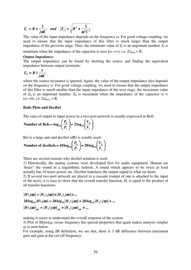
59
22
2 11
CRZand
CjRZ ii
ωωωωωωωω++++====++++====
The value of the input impedance depends on the frequency ω. For good voltage coupling, we
need to ensure that the input impedance of this filter is much larger than the output
impedance of the previous stage. Thus, the minimum value of Zi is an important number. Zi is
minimum when the impedance of the capacitor is zero (ω→∞), i.e. Zi|min = R.
Output Impedance: The output impedance can be found by shorting the source and finding the equivalent
impedance between output terminals:
RZ ====0 ||Cjωωωω
1
where the source resistance is ignored. Again, the value of the output impedance also depends
on the frequency ω. For good voltage coupling, we need to ensure that the output impedance
of this filter is much smaller than the input impedance of the next stage, the maximum value
of Z0 is an important number. Z0 is maximum when the impedance of the capacitor is ∞
(ω→0), i.e. Z0|max = R.
Bode Plots and Decibel
The ratio of output to input power in a two-port network is usually expressed in Bell:
====
====
ii V
V
P
P 0
10
0
10 log2log Bels ofNumber
Bel is a large unit and decibel (dB) is usually used:
====
====
ii V
V
P
P 0
10
0
10 log20log10 decibels ofNumber
There are several reasons why decibel notation is used:
1) Historically, the analog systems were developed first for audio equipment. Human ear
‘hears" the sound in a logarithmic fashion. A sound which appears to be twice as loud
actually has 10 times power, etc. Decibel translates the output signal to what ear hears.
2) If several two-port network are placed in a cascade (output of one is attached to the input
of the next), it is easy to show that the overall transfer function, H, is equal to the product of
all transfer functions:
...)()()(
...)(log20)(log20)(log20
...)()()(
21
21011010
21
++++++++====
++++++++====
××××××××====
dBdBdBjHjHjH
jHjHjH
jHjHjH
ωωωωωωωωωωωω
ωωωωωωωωωωωω
ωωωωωωωωωωωω
making it easier to understand the overall response of the system.
3) Plot of |H(jω)|dB versus frequency has special properties that again makes analysis simpler
as is seen below.
For example, using dB definition, we see that, there is 3 dB difference between maximum
gain and gain at the cut-off frequency:
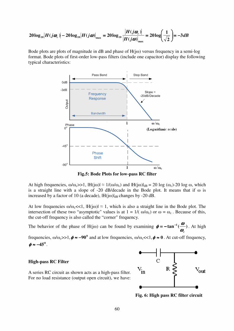
60
dBjH
jHjHjH
c
c 32
1log20
)(
)(log20)(log20)(log20
max
10max1010 −−−−====
========−−−−
ωωωω
ωωωωωωωωωωωω
Bode plots are plots of magnitude in dB and phase of H(jω) versus frequency in a semi-log
format. Bode plots of first-order low-pass filters (include one capacitor) display the following
typical characteristics:
Fig.5: Bode Plots for low-pass RC filter
At high frequencies, ω/ωc>>1, |H(jω)| ≈ 1/(ω/ωc) and |H(jω)|dB = 20 log (ωc)-20 log ω, which
is a straight line with a slope of -20 dB/decade in the Bode plot. It means that if ω is
increased by a factor of 10 (a decade), |H(jω)|dB changes by -20 dB.
At low frequencies ω/ωc<<1, |H(jω)| ≈ 1, which is also a straight line in the Bode plot. The
intersection of these two “asymptotic" values is at 1 = 1/( ω/ωc) or ω = ωc . Because of this,
the cut-off frequency is also called the “corner" frequency.
The behavior of the phase of H(jω) can be found by examining )(tan 1
cωωωω
ωωωωφφφφ −−−−−−−−==== . At high
frequencies, ω/ωc>>1, 090−−−−≈≈≈≈φφφφ and at low frequencies, ω/ωc<<1, 0≈≈≈≈φφφφ . At cut-off frequency,045−−−−≈≈≈≈φφφφ .
High-pass RC Filter
A series RC circuit as shown acts as a high-pass filter.
For no load resistance (output open circuit), we have:
Fig. 6: High pass RC filter circuit
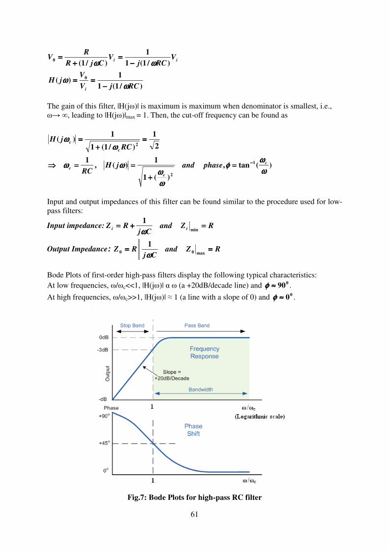
61
)/1(1
1)(
)/1(1
1
)/1(
0
0
RCjV
VjH
VRCj
VCjR
RV
i
ii
ωωωωωωωω
ωωωωωωωω
−−−−========
−−−−====
++++====
The gain of this filter, |H(jω)| is maximum is maximum when denominator is smallest, i.e.,
ω→ ∞, leading to |H(jω)|max = 1. Then, the cut-off frequency can be found as
)(tan,
)(1
1)(,
1
2
1
)/1(1
1)(
1
2
2
ωωωω
ωωωωφφφφ
ωωωω
ωωωωωωωωωωωω
ωωωωωωωω
c
c
c
c
c
phaseandjHRC
RCjH
−−−−====
++++
========⇒⇒⇒⇒
====++++
====
Input and output impedances of this filter can be found similar to the procedure used for low-
pass filters:
Input impedance: RZandCj
RZ ii ====++++====min
1
ωωωω
Output Impedance: RZandCj
RZ ========max00
1
ωωωω
Bode Plots of first-order high-pass filters display the following typical characteristics:
At low frequencies, ω/ωc<<1, |H(jω)| α ω (a +20dB/decade line) and 090≈≈≈≈φφφφ .
At high frequencies, ω/ωc>>1, |H(jω)| ≈ 1 (a line with a slope of 0) and 00≈≈≈≈φφφφ .
Fig.7: Bode Plots for high-pass RC filter
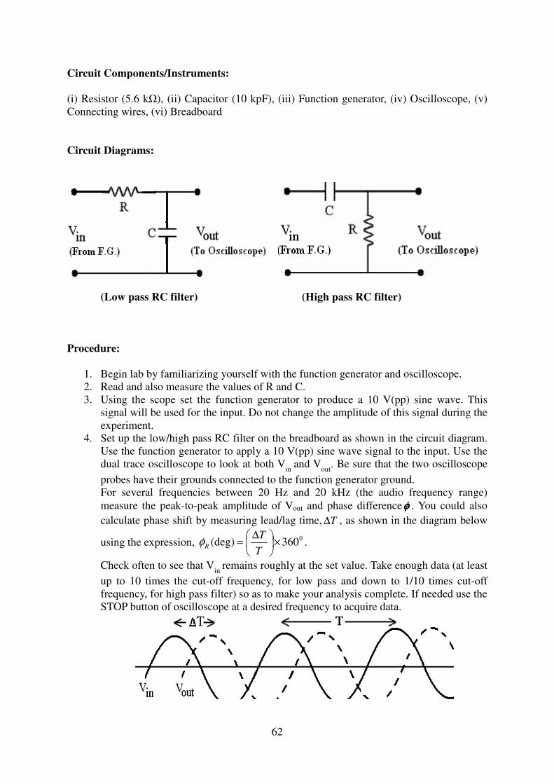
62
Circuit Components/Instruments:
(i) Resistor (5.6 kΩ), (ii) Capacitor (10 kpF), (iii) Function generator, (iv) Oscilloscope, (v)
Connecting wires, (vi) Breadboard
Circuit Diagrams:
(Low pass RC filter) (High pass RC filter)
Procedure:
1. Begin lab by familiarizing yourself with the function generator and oscilloscope.
2. Read and also measure the values of R and C.
3. Using the scope set the function generator to produce a 10 V(pp) sine wave. This
signal will be used for the input. Do not change the amplitude of this signal during the
experiment.
4. Set up the low/high pass RC filter on the breadboard as shown in the circuit diagram.
Use the function generator to apply a 10 V(pp) sine wave signal to the input. Use the
dual trace oscilloscope to look at both Vin
and Vout
. Be sure that the two oscilloscope
probes have their grounds connected to the function generator ground.
For several frequencies between 20 Hz and 20 kHz (the audio frequency range)
measure the peak-to-peak amplitude of Vout and phase differenceφφφφ . You could also
calculate phase shift by measuring lead/lag time, T∆ , as shown in the diagram below
using the expression, 0360(deg) ×
∆=
T
TRφ .
Check often to see that Vin
remains roughly at the set value. Take enough data (at least
up to 10 times the cut-off frequency, for low pass and down to 1/10 times cut-off
frequency, for high pass filter) so as to make your analysis complete. If needed use the
STOP button of oscilloscope at a desired frequency to acquire data.
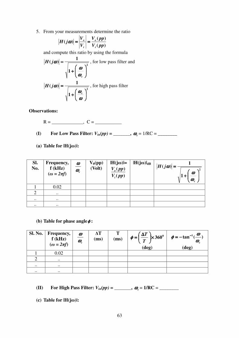
63
5. From your measurements determine the ratio
)(
)()(
ppV
ppV
V
VjH
i
o
i
o ========ωωωω
and compute this ratio by using the formula
2
1
1)(
++++
====
c
jH
ωωωω
ωωωω
ωωωω , for low pass filter and
2
1
1)(
++++
====
ωωωω
ωωωωωωωω
c
jH , for high pass filter
Observations:
R = _____________, C = ___________
(I) For Low Pass Filter: Vin(pp) = _______, cωωωω = 1/RC = ________
(a) Table for |H(jω)|:
Sl.
No.
Frequency,
f (kHz)
(ω = 2πf) cωωωω
ωωωω
V0(pp)
(Volt)
|H(jω)|=
)(
)(
ppV
ppV
i
o
|H(jω)|dB
2
1
1)(
++++
====
c
jH
ωωωω
ωωωω
ωωωω
1 0.02
2 ..
.. ..
.. ..
(b) Table for phase angleφφφφ :
Sl. No. Frequency,
f (kHz)
(ω = 2πf) cωωωω
ωωωω
ΔT
(ms)
T
(ms) 0360××××
∆∆∆∆====
T
Tφφφφ
(deg)
)(tan 1
cωωωω
ωωωωφφφφ −−−−−−−−====
(deg)
1 0.02
2 ..
.. ..
.. ..
(II) For High Pass Filter: Vin(pp) = _______, cωωωω = 1/RC = ________
(c) Table for |H(jω)|:
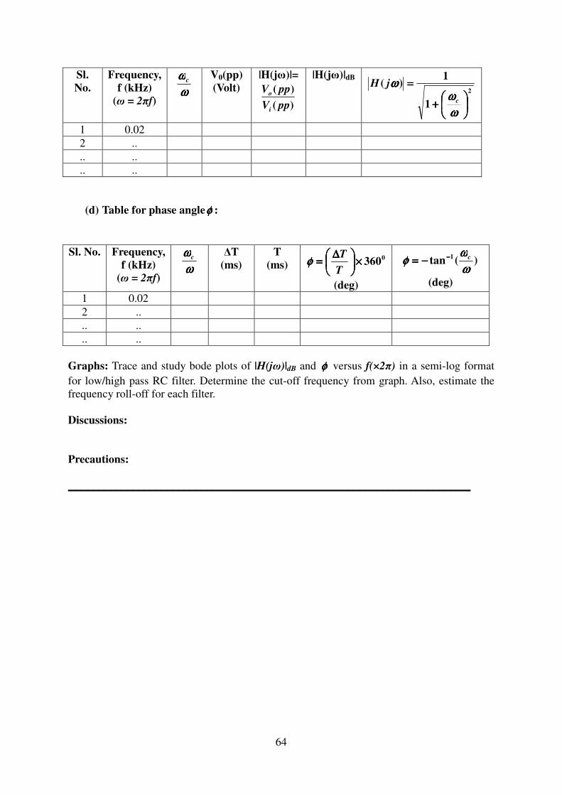
64
Sl.
No.
Frequency,
f (kHz)
(ω = 2πf) ωωωω
ωωωωc V0(pp)
(Volt)
|H(jω)|=
)(
)(
ppV
ppV
i
o
|H(jω)|dB
2
1
1)(
++++
====
ωωωω
ωωωωωωωω
c
jH
1 0.02
2 ..
.. ..
.. ..
(d) Table for phase angleφφφφ :
Sl. No. Frequency,
f (kHz)
(ω = 2πf) ωωωω
ωωωωc ΔT
(ms)
T
(ms) 0360××××
∆∆∆∆====
T
Tφφφφ
(deg)
)(tan 1
ωωωω
ωωωωφφφφ c−−−−−−−−====
(deg)
1 0.02
2 ..
.. ..
.. ..
Graphs: Trace and study bode plots of |H(jω)|dB and φφφφ versus f(×2π) in a semi-log format
for low/high pass RC filter. Determine the cut-off frequency from graph. Also, estimate the
frequency roll-off for each filter.
Discussions:
Precautions:
_______________________________________________________________________

Active Filter
Objectives:
To construct and analyze the frequency response of
(ii) A low pass active filter
(iii) A high pass active filter
(iv) A band pass active filter
Overview:
The main disadvantage of passive filters
previous labs) is the fact that the maximum gain that can be achieved with these filters is 1
other words, the maximum output voltag
circuits using Opamps, then the
The circuits employed are all based on the inverting
placed in the correct position for the particular t
filter circuits because they use
Low-Pass filters - the integrator reconsidered
A low pass filter passes only low frequency signals and attenuates signals of high
frequencies. We have already considered the time response of the integrator circuit, but its
frequency response can also be studied. Figure 1 shows a low pass active filter in inverting
configuration.
Fig. 1: First Order Low Pass Filter with Op Amp
Gain of the above circuit, AV
whereCf
X Cππππ2
1==== , is the impedance of the capacitor and
signal.
65
Active Filter Circuits using Operational amplifi
To construct and analyze the frequency response of
A low pass active filter
A high pass active filter
A band pass active filter
The main disadvantage of passive filters (as you have already seen in one of your
is the fact that the maximum gain that can be achieved with these filters is 1
output voltage is equal to the input voltage. If we make filter
the gain can be greater than 1.
The circuits employed are all based on the inverting Opamps with the addition of a capacitor
placed in the correct position for the particular type of filter. These circuits are called
because they use Opamps which require a power supply.
the integrator reconsidered
A low pass filter passes only low frequency signals and attenuates signals of high
ies. We have already considered the time response of the integrator circuit, but its
frequency response can also be studied. Figure 1 shows a low pass active filter in inverting
Fig. 1: First Order Low Pass Filter with Op Amp
1
2
R
XR C−−−−==== ,
, is the impedance of the capacitor and f is the frequency of the input
iers
(as you have already seen in one of your
is the fact that the maximum gain that can be achieved with these filters is 1. In
e is equal to the input voltage. If we make filter
with the addition of a capacitor
ype of filter. These circuits are called active
A low pass filter passes only low frequency signals and attenuates signals of high
ies. We have already considered the time response of the integrator circuit, but its
frequency response can also be studied. Figure 1 shows a low pass active filter in inverting
is the frequency of the input
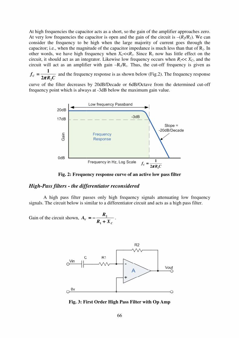
At high frequencies the capacitor acts as a short, so the gain of the amplifier approaches zero.
At very low frequencies the capacitor is open and the gain of the circuit is
consider the frequency to be high when the large majority of current goes through the
capacitor; i.e., when the magnitude of the capacitor impedance is much less than that of
other words, we have high frequency when
circuit, it should act as an integrator. Likewise low frequency occurs when
circuit will act as an amplifier with gain
CRfC
22
1
ππππ==== and the frequency response is as shown below (Fig.2). The frequency response
curve of the filter decreases by 20dB/Decade or 6dB/Octave from the determined cut
frequency point which is alwa
Fig. 2: Frequency response curve
High-Pass filters - the differentiator reconsidered
A high pass filter passes only high frequency signals attenuating low
signals. The circuit below is similar to a differentiator circuit and acts as a high pass filter.
Gain of the circuit shown, VA
Fig. 3: First Order High Pass Filter with Op Amp
66
At high frequencies the capacitor acts as a short, so the gain of the amplifier approaches zero.
frequencies the capacitor is open and the gain of the circuit is
consider the frequency to be high when the large majority of current goes through the
capacitor; i.e., when the magnitude of the capacitor impedance is much less than that of
other words, we have high frequency when XC<<R2. Since R2 now has little effect on the
circuit, it should act as an integrator. Likewise low frequency occurs when
circuit will act as an amplifier with gain –R2/R1. Thus, the cut-off frequency is given as
and the frequency response is as shown below (Fig.2). The frequency response
curve of the filter decreases by 20dB/Decade or 6dB/Octave from the determined cut
frequency point which is always at -3dB below the maximum gain value.
Fig. 2: Frequency response curve of an active low pass filter
the differentiator reconsidered
A high pass filter passes only high frequency signals attenuating low
signals. The circuit below is similar to a differentiator circuit and acts as a high pass filter.
C
VXR
R
++++−−−−====
1
2 .
: First Order High Pass Filter with Op Amp
CRfC
22
1
ππππ====
At high frequencies the capacitor acts as a short, so the gain of the amplifier approaches zero.
frequencies the capacitor is open and the gain of the circuit is –(R2/R1). We can
consider the frequency to be high when the large majority of current goes through the
capacitor; i.e., when the magnitude of the capacitor impedance is much less than that of R2. In
now has little effect on the
circuit, it should act as an integrator. Likewise low frequency occurs when R2<< XC, and the
off frequency is given as
and the frequency response is as shown below (Fig.2). The frequency response
curve of the filter decreases by 20dB/Decade or 6dB/Octave from the determined cut-off
low pass filter
A high pass filter passes only high frequency signals attenuating low frequency
signals. The circuit below is similar to a differentiator circuit and acts as a high pass filter.
67
At high frequencies the capacitor acts as a short, so the gain of the amplifier becomes –R2/R1.
At very low frequencies the capacitor is open and the gain of the circuit approaches 0. For
this circuit, the cut-off frequency is CR
fC
12
1
ππππ==== . However, it has to be kept in mind that
the maximum pass band frequency response of an active high pass filter is limited to the
characteristics or bandwidth of the op-amp being used within the circuit design. In the
previous experiments you have seen that the maximum frequency response of an op-amp is
limited to the Gain/Bandwidth product or open loop voltage gain of the operational amplifier
being used. The frequency response of a high pass filter of gain 40 dB is shown below in Fig.
4. The upper curve is the typical frequency response of the opamp with open-loop. The
frequency response curve of the filter increases by 20dB/Decade or 6dB/Octave up to the
determined cut-off frequency point.
Fig. 4: Frequency response curve of an active high pass filter
Band-Pass Filter
A band-pass filter rejects high and low frequencies, passing signals around some
intermediate frequency only. The simplest band-pass filter can be made by combining the
first order low pass and high pass filters that we just looked at. The cut-off or corner
frequency of the low pass filter (LP) is higher than the cut-off frequency of the high pass
filter (HP) and the difference between the frequencies at the -3dB point will determine the
"Bandwidth" of the filter while attenuating any signals outside of these points.
CRfC
12
1
ππππ====
Fig.
This circuit will attenuate low frequencies
222
1
CRf LP
ππππ==== ( LPf > HPf ), but will pass intermediate frequencies with a gain
However, this circuit cannot be used to make a filter with a very narrow band.
Fig.6: Frequency response curve
Circuit Components/Equipments:
(i) OPAMP (IC741), (ii) Resistors, (iii) Capacitors,
Oscilloscope, (vi) Breadboard, (vii) Connecting wires.
Circuit Diagrams: Refer to Figs 1, 3 and 5.
Procedure:
6. Read/measure the values of all circuit components to be used. Calculate the cut
frequencies in each case.
68
Fig. 5: Band Pass Filter with Op Amp
This circuit will attenuate low frequencies 112
1
CRf HP
ππππ==== and high frequencies
), but will pass intermediate frequencies with a gain
However, this circuit cannot be used to make a filter with a very narrow band.
: Frequency response curve of an active band pass filter
Circuit Components/Equipments:
OPAMP (IC741), (ii) Resistors, (iii) Capacitors, (iv) Function generator, (v)
Oscilloscope, (vi) Breadboard, (vii) Connecting wires.
Circuit Diagrams: Refer to Figs 1, 3 and 5.
the values of all circuit components to be used. Calculate the cut
frequencies in each case.
,
and high frequencies
), but will pass intermediate frequencies with a gain of –R2/R1.
However, this circuit cannot be used to make a filter with a very narrow band.
pass filter
(iv) Function generator, (v)
the values of all circuit components to be used. Calculate the cut-off
, log scale
69
7. Using the scope set the function generator to produce an input voltage of
approximately 100 mV(pp) sine wave.
8. Set up the low/high/band pass active filter on the breadboard as shown in the circuit
diagrams. Connect the function generator to apply input. Use the dual trace
oscilloscope to look at both Vin
and Vout
. Be sure that the two oscilloscope probes
have their grounds connected to the function generator ground. Match the
magnification control both at the probe and the oscilloscope.
9. Set the RANGE of the function generator between 20 Hz to 20 kHz. Measure the
Vin(pp) and Vout(pp). Use digital filter or average options from oscilloscope to
measure voltages whenever needed.
10. From your measurements determine the gain,)(
)(
ppV
ppV
in
o and compare with the
calculated value.
11. Plot log f ~ gain (dB).
Observations:
(III) For Low Pass Filter:
R1=__________, R2 = _______, C=__________,
Max Gain(calculated) = 1
2
R
R−−−− =_________, _____
2
1
2
========CR
f cππππ
Table:
Sl.
No.
Frequency,
f (kHz)
Vin(pp)
(Volt)
Vo(pp)
(Volt)
Gain,AV=
)(
)(
ppV
ppV
i
o
Gain
(dB)
1
2
..
..
(IV) For High Pass Filter:
R1 = _______, R2 = _______, C = ___________,
Max Gain(calculated) = 1
2
R
R−−−− =_________, _____
2
1
1
========CR
fππππ
Table:
Sl.
No.
Frequency,
f (kHz)
Vin(pp)
(Volt)
V0(pp)
(Volt)
Gain,AV=
)(
)(
ppV
ppV
i
o
Gain
(dB)
1
2
..
70
..
(V) For Band Pass Filter:
R1 = _______, R2 = _______, C1 =_______, C2 = _________
Max Gain(calculated) = 1
2
R
R−−−− =_________,
_____2
1
11
========CR
f HPππππ
, ________2
1
22
========CR
f LPππππ
Table:
Sl.
No.
Frequency,
f (kHz)
Vin(pp)
(Volt)
V0(pp)
(Volt)
Gain,AV=
)(
)(
ppV
ppV
i
o
Gain
(dB)
1
2
..
..
Graphs: Plot the frequency response curve for each filter and determine the cut-off
frequencies and frequency roll-off rate (in dB/decade) in each case.
Discussions:
Precautions:
________________________________________________________________________