basic electronics course for the ino graduate training ...bsn/other/basic electronics course.pdf ·...
TRANSCRIPT
Basic Electronics course for the INO Graduate Training programme
B.Satyanarayana
Department of High Energy Physics TIFR, Mumbai INDIA
Email: [email protected] Webpage: http://www.tifr.res.in/~bsn
Contact: 02222782368, 09987537702 Office: C121
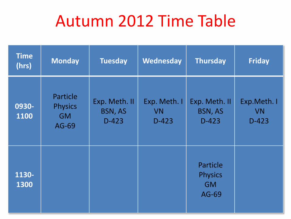
Autumn 2012 Time Table
Time (hrs)
Monday Tuesday Wednesday Thursday Friday
0930-1100
Particle Physics
GM AG-69
Exp. Meth. II BSN, AS D-423
Exp. Meth. I VN
D-423
Exp. Meth. II BSN, AS D-423
Exp.Meth. I VN
D-423
1130-1300
Particle Physics
GM AG-69

Course Outline-1 Basic detector characteristics and output
Charge, current and voltage Signal types: DC or pulse (and pulse shapes)
Passive components Resistors, capacitors, inductors, impedance and transformers Integrators, differentiators, LCR resonant circuits
Generation and measurement of
Voltage, current, time, frequency Measuring resistance, temperature, pressure, magnetic field and light
Basic semiconductor device physics
P-N junction, Diodes, I-V curve
Rectifiers, DC power supplies, regulators, DC-DC converters Transistor characteristics
Transistor circuits: emitter follower, push-pull amplifier Low noise devices: FET, JFET, MOSFET

Course Outline-2 Operational amplifiers
Principle of Negative feedback Differential amplifier Applications: differentiator, integrator, amplifiers, summing amplifier, oscillators, comparators
Noise in detectors and electronics Measurement and reduction of noise Grounding and shielding
Digital electronics
Why digital? Logic states, gates (OR, NOT, AND, NAND, NOR, XOR) Implementing arbitrary truth tables, Karnaugh maps Flip-flops, latches, registers, memories (RAM, ROMs, FIFO etc.) Multiplexers, decoders, mono-stable multi-vibrators, counters
Logic families TTL, CMOS, LVDS
Co-axial cables
Signal transmission and loss Impedance matching Noise and distortion

Course Outline-3 Commonly used front end electronics
Preamplifiers, shaping amplifiers Fast and slow coincidence, logic & linear gates, logic & linear FIFO, delay line Discriminators: leading edge, constant fraction Coincidence circuits Single channel analyser, multi-channel analyser
ADC, DAC and TDC
Performance parameters ADC functions: Charge versus peak sensing ADC types: Wilkinson, successive approximation, flash DAC and applications TDC: Principles, classical types, FPGA, ASIC
Some advanced topics
Programmable logic: CPLD, FPGA Application Specific Integrated Circuits (ASICs)
PC interfacing protocols and standards Serial (RS-232, USB, SPI), parallel (Centronix, PCI) Modular instrumentation standards: NIM, CAMAC, VME

Some info on the course
Good news! The course will be taught at introductory rather than advanced level. You will be possibly be prepared to setup and run nuclear and high energy
physics experiments. No. of class room hours = 30 hours (approx.), i.e. 20 x 1.5 hours Class days and hours: Tuesdays and Thursdays, 9:30am to 11am Class room: D-423 Teaching method: PPT projection + blackboard A few additional guest lectures on specific topics are planned. Assessment: Four assignments = 20 marks Mid semester exam = 25 marks End semester exam = 40 marks Case-study work = 15 marks

Some references
Stefaan Tavernier, Experimental Techniques in Nuclear and Particle Physics, Springer (2010). G.F. Knoll, Radiation detection and measurement, John Wiley & Sons
(2000). W.R.Leo, Techniques for Nuclear and Particles Physics Experiments,
Narosa (1987) Anant Agarwal & Jeffrey H. Lang, Foundations of Analog and Digital
Electronic Circuits, Morgan Kaufmann (2006) Paul Horowitz & Winfield Hill, The Art of Electronics, Cambridge
University Press (1980) Albert Paul Malvino, Electronic Principles, Tata McGraw-Hill (2007) Thankful to these authors. A lot of material and figures from the above
mentioned books will be used in this course.

LECTURE-1 August 16, 2012

Basic detector characteristics and output
• Detection of ionising radiation in the end nearly always comes down to detecting some small electrical signal.
• Dealing with such small signals is one of the main challenges in designing detectors for nuclear physics and particle physics.
• From the electrical point of view, a detector is a current source with a large internal resistance and a small capacitance.
• In the absence of any ionising radiation there is a small current, which is called the dark current or leakage current.

Modes for measuring detector signals
Current mode Measures the total current of the detector and ignores
the pulse nature of the signal. Does not allow advantage to be taken of the timing and
amplitude information present in the signal.
Pulse mode. Observes and counts the individual pulses generated by
the particles. Gives superior performance but cannot be used if the
rate is too large.

Current mode If we set the open loop gain of the operational amplifier as A, the characteristics of the feedback circuit allows the equivalent input resistance to be which is several orders of magnitude smaller than Rf. Thus this circuit enables ideal Isc measurement over a wide range.

An example of pulse mode
inVR
R
1
2oV
Voltage amplifier
Charge amplifier

Pulse mode
Amplitude of the pulses is proportional to the initial charge signal and the arrival time of the pulse is some fixed time after the physical event. By using appropriate thresholds, one can select and count
only those pulses that one wants to count. Often the ‘good events’ are characterised by some specific signal amplitude simultaneous presence of two (or more) signals in different
detectors. absence of some other signal.
In the pulse mode, one can register a pulse height spectrum and such a spectrum contains a large amount of useful information.

LECTURE-2 August 21, 2012

Pulse counting
A discrimination circuit has an analog input signal and a digital output signal. If the input signal exceeds some fixed threshold, a digital output signal is generated.
• In this process, the setup could be inefficient.
• Sometimes a real event in the detector does not produce a pulse that is large enough to produce a signal exceeding the threshold.
• Or a suitable signal was produced, but the electronics did not recognise the pulse because it was arriving at the same time as some other event.
• This last effect is referred to as dead time.

Coincidence of signals
• To see if an event occurred simultaneously with some other event, the electronics will look for the simultaneous presence of two logical signals within some time Window.
• In coincidence counting, one should be aware of the possibility to have random coincidences.
• These are occurrences of a coincidence caused by two unrelated events arriving by chance at the same time.
• The rate of random coincidences between two signals is proportional to the rate of each type of signal times the duration of the coincidence window.
t21
dt
dN
dt
dN
dt
dN random

Triad of passive linear elements
Resistors Capacitors Inductors

Resistors
At the bottom, Silicon-chromium thin-film resistors, each with 6 μm width and 217.5 μm length, and nominal resistance 50 k
Nichrome wire used in toasters and electric stoves and planar layers of poly-silicon in highly complex computer chips, to small rods of carbon particles encased in Bakelite commonly found in electronic equipment ...
Voltage measured across the terminals of a resistor is linearly proportional to the current flowing through the resistor. The constant of proportionality is called the resistance
v = iR (Ohm’s Law)
a
lR
Resistance of a cuboid shaped resistor with length l, width w, and height h is given by
R = ρl/wh

Material ρ (Ω•m) at 20 °C σ (S/m) at 20 °C Temperature
coefficient[note 1] (K−1)
Reference
Silver 1.59×10⁻⁸ 6.30×10⁷ 0.0038 [4][5]
Copper 1.68×10⁻⁸ 5.96×10⁷ 0.0039 [5]
Annealed copper[note 2] 1.72×10⁻⁸ 5.80×10⁷ [citation needed]
Gold[note 3] 2.44×10⁻⁸ 4.10×10⁷ 0.0034 [4]
Aluminium[note 4] 2.82×10⁻⁸ 3.5×10⁷ 0.0039 [4]
Calcium 3.36×10⁻⁸ 2.98×10⁷ 0.0041
Tungsten 5.60×10⁻⁸ 1.79×10⁷ 0.0045 [4]
Zinc 5.90×10⁻⁸ 1.69×10⁷ 0.0037 [6]
Nickel 6.99×10⁻⁸ 1.43×10⁷ 0.006
Lithium 9.28×10⁻⁸ 1.08×10⁷ 0.006
Iron 1.0×10⁻⁷ 1.00×10⁷ 0.005 [4]
Platinum 1.06×10⁻⁷ 9.43×10⁶ 0.00392 [4]
Tin 1.09×10⁻⁷ 9.17×10⁶ 0.0045
Carbon steel (1010) 1.43×10⁻⁷ 6.99×10⁶ [7]
Lead 2.2×10⁻⁷ 4.55×10⁶ 0.0039 [4]
Titanium 4.20×10⁻⁷ 2.38×10⁶ X
Grain oriented electrical steel 4.60×10⁻⁷ 2.17×10⁶ [8]
Manganin 4.82×10⁻⁷ 2.07×10⁶ 0.000002 [9]
Constantan 4.9×10⁻⁷ 2.04×10⁶ 0.000008 [10]
Stainless steel[note 5] 6.9×10⁻⁷ 1.45×10⁶ [11]
Mercury 9.8×10⁻⁷ 1.02×10⁶ 0.0009 [9]
Nichrome[note 6] 1.10×10⁻⁶ 9.09×10⁵ 0.0004 [4]
GaAs 5×10⁻⁷ to 10×10−3 5×10⁻⁸ to 103 [12]
Carbon (amorphous) 5×10⁻⁴ to 8×10⁻⁴ 1.25 to 2×10³ −0.0005 [4][13]
Carbon (graphite)[note 7] 2.5e×10−6 to 5.0×10⁻⁶ //basal plane 3.0×10⁻³ ⊥basal plane
2 to 3×10⁵ //basal plane 3.3×10² ⊥basal plane
[14]
Carbon (diamond)[note 8] 1×10¹² ~10−13 [15]
Germanium[note 8] 4.6×10⁻¹ 2.17 −0.048 [4][5]
Sea water[note 9] 2×10⁻¹ 4.8 [16]
Drinking water[note 10] 2×101 to 2×10³ 5×10⁻⁴ to 5×10⁻² [citation needed]
Silicon[note 8] 6.40×10² 1.56×10⁻³ −0.075 [4]
Deionized water[note 11] 1.8×10⁵ 5.5×10⁻⁶ [17]
Glass 10×1010 to 10×1014 10−11 to 10−15 ? [4][5]
Hard rubber 1×10¹³ 10−14 ? [4]
Sulfur 1×10¹⁵ 10−16 ? [4]
Air 1.3×10¹⁶ to 3.3×10¹⁶ 3×10⁻¹⁵ to 8×10⁻¹⁵ [18]
Paraffin 1×10¹⁷ 10−18 ?
Fused quartz 7.5×10¹⁷ 1.3×10⁻¹⁸ ? [4]
PET 10×1020 10−21 ?
Teflon 10×1022 to 10×1024 10−25 to 10−23 ?
Res
isti
viti
es o
f va
rio
us
mat
eria
ls

Resistance of planar materials Suppose resistance of a planar material of unit length and unit width, W is Ro, then Ro = ρ1/H
Resistance of a cuboid shaped material with length L, width W, height H, and resistivity ρ is R = ρL/WH
Substituting Ro = ρ/H, we get
R = Ro(L/W)

Process shrinks P
leas
e re
ad A
nan
t A
garw
al

Capacitors
Frequency dependent resistors Waveform generation, filtering, blocking and bypass Energy storage, resonant circuits Integrators and differentiators Capacitors can not dissipate power, Why?

Capacitors
dt
dVCI
CVQ

LECTURE-3 August 23, 2012

Inductors
Along with capacitors used to built filters – separate desired signals from background. Capacitors, for practical reasons, are closer to ideal in their behavior than
inductors. In addition, it is easier to place capacitors in integrated circuits, than it is to use inductors. Therefore, we see capacitors being used far more often than we see inductors being used. Still, there are some applications where inductors simply must be used.
Transformers are a case in point. An inductor obeys the expression
where vL is the voltage across the inductor, and iL is the current through the
inductor, and LX is called the inductance.
LL X
div L
dt

Transformers
Two closely coupled coils – primary and secondary Voltage multiplication proportional to the turns ratio
of the transformer Current correspondingly reduced Transformers are quite efficient Two important functions Change the ac line voltage to a useful value Isolate the electronic device from actual power line
Transformers for audio and RF (tuned transformers if only narrow range of frequencies present) Transformers for RF use special core materials for
minimising code losses.

Impedance and reactance

Differentiators
Differentiators are used for detecting leading edges and training edges in pulse circuits.
Make sure that R is “not too small”, thus loading the input


Unintentional capacitive coupling

Integrators
Integrators find use in analog computation, control systems, feedback, analog/digital conversion and waveform generation.

A simple application of integrator
LECTURE-4 September 3, 2012

Lab course
RPC fabrication and characterisation Muon life time Atmospheric muon flux monitoring using RPC stack in C217

Devices in which a controlled flow of electrons can be obtained are the basic building blocks of all the
electronic circuits.
Solid-state semiconductor electronics (Since ~1930’s)
Some solid state semiconductors and their junctions offer the
possibility of controlling the number and direction of flow of charge carriers through them.
Simple excitations like light, heat or small applied voltage etc. can
change the number of mobile charges in semiconductors. Supply and flow of charge carriers in the semiconductors are within
the solid itself. Advantages: Small, low voltage, low power, long life, high reliability

Metals, semiconductors and insulators
Current flow due to the applied field
j = E/
where j is the current density, E is the field applied and is the resistivity.
Classification based on resistivity
Metals = 10-2 to 10-8 Ω-m is fairly independent of E α T
Semiconductors = 10-5 to 106 Ω-m α 1/T
Insulators = 1011 to 1019 Ω-m

Band gap theory
• Inside crystal each electron has different energy level; decided by the orbit in which it revolves
• Energy levels with continuous energy variation Energy bands
• Valence energy band and conduction energy band
• The gap between top of valence band and bottom of conduction band is called the Energy gap Eg

Classification based on energy bands
Conductors Conduction band partially full and valence band is partially empty. Electrons from lower
bands can move up
Conduction and valence bands overlap
Insulators Eg high (~6eV); No electrons in the conduction band
Semiconductors Eg low (~1eV); Electrons can acquire enough energy to cross from valence to conduction
band

p-n junction
A clear understanding of the junction behaviour is important to analyse the working of other semiconductor devices.
How a junction is formed and how the junction behaves under the influence of external applied voltage (also called bias).

How does a p-n junction formed? By adding precisely a small quantity of impurity, part of the p-Si wafer can be converted into n-Si. The wafer
now contains p-region and n-region and a metallurgical junction between p-, and n- regions. Two important processes occur during the formation of a p-n junction: diffusion and drift. Due to the concentration gradient across p-, and n- sides, holes diffuse from p-side to n-side (p n) and
electrons diffuse from n-side to p-side (n p). This motion of charge carries gives rise to diffusion current across the junction.
As the electrons continue to diffuse from n p, a layer of positive charge (or positive space-charge region) on
n-side of the junction is developed. Similarly negative charge is developed on p-side. This space-charge region on either side of the junction together is known as depletion region. The thickness of
depletion region is of the order of one-tenth of a micron. An electric field directed from positive charge towards negative charge develops. Due to this field, an electron
on p-side of the junction moves to n-side and a hole on n-side of the junction moves to p-side. The motion of charge carriers due to the electric field is called drift. Thus a drift current, which is opposite in direction to the diffusion current starts.

Initially, diffusion current is large and drift current is small. As the diffusion process continues, the space-charge regions on either side of the junction extend, thus increasing the electric field strength and hence drift current. This process continues until the diffusion current equals the drift current. Thus a p-n junction is formed. In a p-n junction under equilibrium there is no net current.
The loss of electrons from the n-region and
the gain of electrons by the p-region cause a difference of potential across the junction of the two regions. The polarity of this potential is such as to oppose further flow of carriers so that a condition of equilibrium exists. Since this potential tends to prevent the movement of electron from the n region into the p region, it is often called a barrier potential.

Semiconductor diode
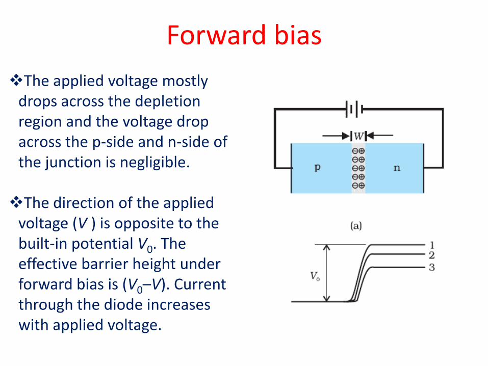
Forward bias
The applied voltage mostly drops across the depletion region and the voltage drop across the p-side and n-side of the junction is negligible.
The direction of the applied
voltage (V ) is opposite to the built-in potential V0. The effective barrier height under forward bias is (V0–V). Current through the diode increases with applied voltage.

Due to the applied voltage, electrons from n-side cross the depletion region and reach p-side (where they are minority carries). Similarly, holes from p-side cross the junction and reach the n-side (where they are minority carries). This process under forward bias is known as minority carrier injection.
At the junction boundary, on each side, the minority carrier concentration
increases significantly compared to the locations far from the junction. Due to this concentration gradient, the injected electrons on p-side diffuse from the junction edge of p-side to the other end of p-side. Likewise, the injected holes on n-side diffuse from the junction edge of n-side to the other end of n-side. This motion of charged carriers on either side gives rise to current.
The total diode forward current is sum of hole diffusion current and conventional
current due to electron diffusion. The magnitude of this current is usually in mA.

Current components in a p-n diode

Reverse bias
The applied voltage mostly drops across the depletion region. The direction of applied voltage is same as the direction of barrier potential.
As a result, the barrier height increases and
the depletion region widens due to the change in the electric field. The effective barrier height under reverse bias is (V0 + V ).
This suppresses the flow of electrons from
n p and holes from p n. Thus, diffusion current, decreases enormously compared to the diode under forward bias.

The electric field direction of the junction is such that if electrons on p-side or holes on n-
side in their random motion come close to the junction, they will be swept to its majority
zone. This drift of carriers gives rise to current. The drift current is of the order of a few µA.
This is quite low because it is due to the motion of carriers from their minority side to their
majority side across the junction. The drift current is also there under forward bias but it is
negligible (µA) when compared with current due to injected carriers which is usually in mA.
The diode reverse current is not very much dependent on the applied voltage. Even a small
voltage is sufficient to sweep the minority carriers from one side of the junction to the other
side of the junction. The current is not limited by the magnitude of the applied voltage but is
limited due to the concentration of the minority carrier on either side of the junction.
The current under reverse bias is essentially voltage independent upto a critical reverse bias
voltage, known as breakdown voltage (Vbr ). When V = Vbr, the diode reverse current
increases sharply. Even a slight increase in the bias voltage causes large change in the
current. If the reverse current is not limited by an external circuit below the rated value
(specified by the manufacturer) the p-n junction will get destroyed due to overheating. This
can happen even for the diode under forward bias, if the forward current exceeds the rated
value.

V-I characteristics of a diode
In forward bias measurement, we use a milli-ammeter since the expected current is large while a micro-ammeter is used in reverse bias to measure the current.

Threshold voltage or cut-in voltage (~0.2V for germanium diode and ~0.7 V for silicon diode). For the diode in reverse bias, the current is very small (~µA) and almost remains constant with change in bias. It is called reverse saturation current (I0). However, for special cases, at very high reverse bias (break down voltage), the current suddenly increases. The general purpose diodes are not used beyond the reverse saturation current region.
(26mV at room temperature)
I0 is the saturation current, VT is the thermal voltage, is the ideality factor, also known as the quality factor or sometimes emission coefficient (1 for Ge and 2 for Si)), I = Diode current, V is the voltage across the diode

Dynamic resistance of a diode
p-n junction diode
primarily allows the
flow of current only in
one direction (forward
bias). The forward bias
resistance is low as
compared to the
reverse bias resistance.
This property is used
for rectification of ac
voltages.
Small change in voltage
Dynamic resistance of a diode = ------------------------------- Small change in current

Diode as a rectifier
The reverse saturation current of a diode is negligible and can be considered equal to zero for practical purposes.
The reverse breakdown
voltage of the diode must be sufficiently higher than the peak ac voltage at the secondary of the transformer to protect the diode from reverse breakdown.

Input sinusoidal waveform Average value = 0
We will idealise of diode characteristics.
vi = Vmsinωt
i = ImSinωt where 0 ≤ ωt ≤ π
i = 0 where π ≤ ωt ≤ 2π
Im = Vm / (Rf + RL)
Idc = Im / π
Irms = Im / 2
Vdc = -Im * RL / π
Peak inverse voltage = Peak transformer secondary voltage
% regulation = 100 * (Vno load – Vfull load) / Vfull load
Vdc = Vm / π - Idc* Rf
Ripple factor = rms value /average value
r = = 1.21
Parameters
for HWR

Full-wave rectifier
For a full-wave rectifier the secondary of the transformer is provided with a centre tapping and so it is called centre-tap transformer.

Parameters for FWR
Idc = 2Im / π
Irms =
Vdc = -Im * RL / π
Peak inverse voltage = 2 * Max transformer voltage
% regulation = 100 * (Vno load – Vfull load) / Vfull load
Vdc = 2Vm / π - Idc * Rf
Ripple factor = rms value /average value
r = = 0.482

Filters The rectified voltage is in the form of pulses of the shape of half sinusoids. Though it is
unidirectional it does not have a steady value. To get steady dc output from the pulsating voltage normally a capacitor is connected
across the output terminals (parallel to the load RL). Since these additional circuits appear to filter out the ac ripple and give a pure dc voltage, so they are called filters.
When the voltage across the capacitor is rising, it gets charged. If there is no external
load, it remains charged to the peak voltage of the rectified output. When there is a load, it gets discharged through the load and the voltage across it begins to fall. In the next half-cycle of rectified output it again gets charged to the peak value.
The rate of fall of the voltage across the capacitor depends upon the time constant
(1/RLC).

LECTURE-5 September 6, 2012


LECTURE-6 September 11, 2012


The 'metal' in the name MOSFET is now often a misnomer because the previously metal gate material is now often a layer of polysilicon. Aluminium had been the gate material until the mid 1970s, when polysilicon became dominant, due to its capability to form self-aligned gates. Metallic gates are regaining popularity, since it is difficult to increase the speed of operation of transistors without metal gates. Likewise, the 'oxide' in the name can be a misnomer, as different dielectric materials are used with the aim of obtaining strong channels with applied smaller voltages.


• When the gate voltage VGS is below the threshold for making a conductive channel; there is little or no conduction between the terminals source and drain; the switch is off.
• When the gate is more positive, it attracts electrons, inducing an n-type conductive channel in the substrate below the oxide, which allows electrons to flow between the n-doped terminals; the switch is on.
Cut-off (VGS < Vth), linear (VGS > Vth and VDS < ( VGS – Vth )) or saturation (VGS > Vth and VDS > ( VGS – Vth )) modes of operation

Charge amplifier


CMOS – for low power applications
The MOSFET is used in digital complementary metal–oxide–semiconductor (CMOS) logic, which uses p- and n-channel MOSFETs as building blocks. Overheating is a major concern in integrated circuits since ever more
transistors are packed into ever smaller chips. CMOS logic reduces power consumption because no current flows (ideally),
and thus no power is consumed, except when the inputs to logic gates are being switched. CMOS accomplishes this current reduction by complementing every
nMOSFET with a pMOSFET and connecting both gates and both drains together. A high voltage on the gates will cause the nMOSFET to conduct and the
pMOSFET not to conduct and a low voltage on the gates causes the reverse. During the switching time as the voltage goes from one state to another,
both MOSFETs will conduct briefly. This arrangement greatly reduces power consumption and heat generation.


LECTURE-7 September 18, 2012


LECTURE-8 September 20, 2012


LECTURE-9 September 25, 2012


LECTURE-10 September 27, 2012


LECTURE-11 October 23, 2012


Discrete digital circuits
For example, in case of the 7400 IC, 4 circuits of 2 input NAND gate are housed. In case of 7404, 6 circuits of inverter are housed. These are separate ICs. Therefore, to compose a circuit, it is necessary to do each wiring among the pins using the printed board.

Typical computer system

Memory organisation


Multiplexer

Decoder
Example application

LECTURE-12 October 25, 2012

Monostable Multivibrator/ Single Shot multivibrators As the name indicates, Monostable Multivibrators having only single Stable State and the other is QUASI stable state. 1. Positive edge Triggered 2. Negative edge Triggered 3. Level Triggered By giving an input trigger the monostable/ single shot multivibrator generates an output voltage corresponding to the time predetermined by the circuit elements (RC network). ie; The output wave extends as long as the time constant determined by RC network and come back to its reference position. So Monostable Multivibrator produce a Single Shot of output voltage for a trigger pulse. If their is no trigger, the output voltage will be zero. In monostable multivibrator, the HIGH state is called QUASI STABLE state because, it is not stable in output waveform. ie; the output will returns to LOW state after the time t.

Monostable multivibrator


What is a CPLD?
• In case of CPLD, it has wiring among the logic in the IC. So, the wiring on the printed board can be made little.
• A lot of logic devices are housed in CPLD and those connections can be specified by the program.
• The capacity of CPLD is limited. There is limitation on the number of the pins, too.
• It is possible to rewrite CPLD many times because it is recording the contents of the circuit to the flash memory.
• In-situ programming of the chip possible.
Top side Bottom side

EPROM programmable switches

Structure of a FPGA

SRAM controlled programmable switches

TTL AND CMOS
TTL (transistor-transistor logic) and CMOS (complementary MOS) are the two most popular logic families in current use.
TTL NAND gate CMOS AND gate.


Wired-OR"
Driving external loads

TTL and CMOS characteristics
Supply voltage: TTL families require +5 volts, whereas the CMOS families have a wider range: +2 to +15 volts
Input: A TTL input held in the LOW state sources current into
whatever drives it , so to pull it LOW you must sink current. Since the TTL output circuit is good at sinking current, this presents no problem when TTL logic is wired together, but you must keep it in mind when driving TTL with other circuitry. By contrast, CMOS has no input current.

TTL and CMOS characteristics
The TTL input logic threshold is about two diode drops above ground (about 1.3V), whereas most CMOS families have their threshold nominally at half the supply voltage. The HCT and ACT CMOS families are designed with a low threshold similar to bipolar TTL for compatibility, since a bipolar TTL output does not swing all the way to +5 volts.
CMOS inputs are susceptible to damage from static electricity during handling. In both families, unused inputs should be tied HIGH or LOW, as necessary

TTL and CMOS characteristics
Output: The TTL output stage is a saturated transistor to ground in the LOW state. For all CMOS families the output is a turned-on MOSFET, either to ground or to V+; i.e., rail-to-rail output swings.
Speed and power: The bipolar TTL families consume considerable
quiescent current. The corresponding speeds go from about 25MHz to about 100MHz. All CMOS families consume zero quiescent current. However, their power consumption rises linearly with increasing frequency, and CMOS operated near its upper frequency limit often dissipates as much power as the equivalent bipolar TTL family. The speed range of CMOS goes from about 2MHz to about l00MHz.

Families of TTL and CMOS ICs Bipolar
74 - the "standard TTL" logic family had no letters between the "74" and the specific part number. 74L - Low power (compared to the original TTL logic family), very slow H - High speed (still produced but generally superseded by the S-series, used in 1970s era computers) S - Schottky (obsolete) LS - Low Power Schottky AS - Advanced Schottky ALS - Advanced Low Power Schottky F - Fast (faster than normal Schottky, similar to AS)
CMOS C - CMOS 4–15 V operation similar to buffered 4000 (4000B) series HC - High speed CMOS, similar performance to LS, 12 nS HCT - High speed, compatible logic levels to bipolar parts AC - Advanced CMOS, performance generally between S and F AHC - Advanced High-Speed CMOS, three times as fast as HC ALVC - Low voltage - 1.65 to 3.3 V, Time Propagation Delay (TPD) 2 nS AUC - Low voltage - 0.8 to 2.7 V, TPD < 1.9 [email protected] V FC - Fast CMOS, performance similar to F LCX - CMOS with 3 V supply and 5 V tolerant inputs LVC - Low voltage – 1.65 to 3.3 V and 5 V tolerant inputs, tpd < 5.5 [email protected] V, tpd < 9 [email protected] V LVQ - Low voltage - 3.3 V LVX - Low voltage - 3.3 V with 5 V tolerant inputs VHC - Very High Speed CMOS - 'S' performance in CMOS technology and power

Elimination of noise by using differential signaling
In differential signaling, the transmitter translates the single input signal into a pair of outputs that are driven 180° out of phase. Since external interference tend to affect both the wires together, the receiver recovers the signal as the difference in the voltages on the two lines thus improving immunity to such problems. This transmission scheme provides large common-mode rejection and noise immunity to a data transmission system that a single-ended system referenced only to ground cannot provide.

Advantages of LVDS •Ability to reject common-mode noise When the two lines of a differential pair run adjacent and in close proximity to one another, environmental noise, such as EMI (electromagnetic interference), is induced upon each line in approximately equal amounts. Because the signal is read as the difference between two voltages, any noise common to both lines of the differential pair is subtracted out at the receiver. The ability to reject common-mode noise in this manner makes LVDS less sensitive to environmental noise and reduces the risk of noise related problems, such as crosstalk from neighboring lines. •Reduced amount of noise emission When the two adjacent lines of a differential pair transmit data, current flows in equal and opposite directions, creating equal and opposite electromagnetic fields that cancel one another. The strength of these fields is proportional to the flow of current through the lines. Thus the lower current flow in an LVDS transmission line produces a weaker electromagnetic field than other technologies. •Flexibility around their power supply LVDS offers designers flexibility around their power supply solution, working equally well at 5V, 3.3V and lower.

LECTURE-13 November 1, 2012

Transmission of data •Real systems are often distributed Data source is remote from signal processing Instruments in hazardous or very remote environment • Eg. satellites, HEP, nuclear reactors,..,
But also applies to much shorter distances - like nearby labs or instruments in the same room Need to transfer data from source to receiver And usually send messages (eg. control signals) back
Need to understand Practical ways of doing this Issues: power, speed, noise,… other physical constraints
Methods - a mixture Electrical, but increasing use of optical fibres, Radio for satellites and space, mobile telephones,...

Electrical transmission lines

Cables

Coaxial cable

Coaxial cable properties

Termination and Matching

Reflections & terminations of a transmission line

To match or not? (i)
Impedance matching is a general question, not only for transmission lines Match if to transfer maximum power to load (source must be capable) • eg audio speakers
minimise reflections from load • very important in audio, fast (high frequency) systems, to avoid ringing • or multiple pulses (eg in counting systems)
fast pulses • pulse properties can contain important information • usually don't want to change • sometimes we wish to do this with "too fast" signals - "spoiling"
Usually match by choosing impedances, adding voltage buffers transformer matching is another method if this is impractical

To match or not? (ii)
Don't match if High impedance source with small current signals - typical of many
sensors • photodiode, or other sensors must drive high impedance load • short cables are required to avoid difficulties
Weak voltage source, where drawing power from source would affect result • eg bridge circuits
require to change properties of fast pulse • eg pulse widening for ease of detection
electronics with limited drive capabilities • eg logic circuits, many are designed to drive other logic, not long lines • CMOS circuits, even with follower, are an example
If you get this wrong, often end up with new time constants in the system • or prevent system from working at all, eg diode with low R load

Coaxial cable limits
Transmission speed and bandwidth limiting all cables have finite resistance (though remarkably small) for long cables, RC time constant per unit length becomes noticeable therefore expect delay, attenuation and finite rise time in fast pulses
When is a cable a transmission line? not reasonable to assume transmission line behaviour unless length of
line is at least ~ 1/8 wavelength
Other forms of transmission line in high speed circuits, tracks must be laid out carefully using knowledge
of the characteristics of the boards to control delays, rise times and signal velocities eg parallel tracks,... often need measurement to define parameters precisely ultra high frequencies need waveguides or alternative

Pulse distortions in cables
Signal losses in a transmission line arise from resistance in the conductors and leakage through the dielectric. In addition, some loss may also result from electromagnetic radiation; however, this effect is small, especially in coaxial cables with their inherent shielding, and can be neglected for most purposes.
As frequency of the signal increases, the current in the conductors confines itself to thinner and thinner layers near the conductor surface. The effective cross-sectional area of the conductor is thus reduced and its resistance increased. For a coaxial cable, this results in a resistance per unit length which varies approximately as the square root of the frequency and inversely as the inner and outer radii.

Pulse distortions in cables
Good reference: Leo, Chapter 9
LECTURE-14 November 6, 2012

Common pulse processing functions

LECTURE-15 SUDESHNA DASGUPTA
November 12, 2012

LECTURE-16 November 20, 2012

Common pulse processing functions

Preamplifiers
The amplifier serves two main purposes: 1) amplify the signal from the preamplifier 2) shape it to a convenient form for further processing.

Resistive vs Optical Feedback

Need for pulse shaping

CR-RC shapers
CR-RC
CR-RC-CR
Pole-Zero Cancellation

Res
po
nse
of
CR
-RC
sh
aper

Pole
-zer
o c
ance
llati
on

Delay line shaping

Biased amplifiers

Linear gates


LECTURE-17 November 22, 2012

HMC preamp output pulses
Rise time: 2 to 3ns Pulse height: 100-500mV

Two common problems Walk (due to variations in
the amplitude and rise time, finite amount of charge required to trigger the discriminator) Jitter (due to intrinsic
detection process – variations in the number of charges generated, their transit times and multiplication factor etc.)
Considerations for discriminators

Leading edge triggering Fast zero-crossing triggering Constant fraction triggering Amplitude and rise time compensated triggering
Types of discriminators

Fine with if input amplitudes restricted to small range. For example: With 1 to 1.2 range, resolution is
about 400ps. But at 1 to 10 range, the walk
effect increases to ±10ns.
That will need off-line corrections for time-walk using charge or time-over-threshold (TOT) measurements.
Leading edge discriminators

Off-line corrections of time-walk

Zero-crossing and Constant fraction
Zero-crossing Triggering: Timing resolution 400ps, if amplitude range is 1 to 1.2 Timing resolution 600ps, even if the amplitude range is 1 to 10 But, requires signals to be of constant shape and rise-time.

CF and ARC triggering

Basic coincidence technique

Fast-slow coincidence circuits

LECTURE-18 November 29, 2012

Analogue to Digital Conversion
Turns electrical input (voltage/current) into numeric value
Parameters and requirements Resolution • the granularity of the digital values
Integral Non-Linearity • proportionality of output to input
Differential Non-Linearity • uniformity of digitisation increments
Conversion time • how much time to convert signal to digital value
Count-rate performance • how quickly a new conversion can begin after a previous event
Stability • how much values change with time

Analog-to-Digital Converters (ADCs)
Peak-sensing Maximum of the voltage signal is digitised Ex: Signal of the PMT in voltage mode (slow signals,
already integrated)
Charge sensitive Total integrated current digitised Ex: Signal of the PMT in the current mode (fast signals)
Time of integration or the time period over which the ADC seeks a maximum is determined by the width of the gate signal

Types of ADCs
Ramp or Wilkinson Successive approximation Flash or parallel Sigma-delta ADC Hybrid (Wilkinson + successive approximation) Tracking ADC Parallel ripple ADC Variable threshold flash ADC …

Ramp or Wilkinson ADC

Successive approximation ADC

• Flash ADC is the fastest ADC type available. The digital equivalent of the analog signal will be available right away at it output – hence the name “flash”.
• The number of required comparers is 2n-1, where n is the number of output bits.
• Since Flash ADC comparisons are set by a set of resistors, one could set different values for the resistors in order to obtain a non-linear output, i.e. one value would represent a different voltage step from the other values.
Flash or parallel ADC
LECTURE-19 December 11, 2012

Sigma-delta ADC

• Output value D should be linearly proportional to V
• Check with plot
• For more precise evaluation of INL fit to line and plot deviations
• Plot Di-Dfit vs nchan
Integral non-linearity

Differential non-linearity • Measures non-uniformity in channel profiles over range
DNL = DV i/<DV> - 1 DV i = width of channel i <DV> = average width
• RMS or worst case values may be quoted DNL ~ 1% typical but 10-3 can be achieved can show up systematic effects, as well as random

Resolution

Other variables
Conversion time finite time is required for conversion and storage of values may depend on signal amplitude gives rise to dead time in system i.e. system cannot handle another event during dead time may need accounting for, or risk bias in results
Rate effects results may depend on rate of arrival of signals typically lead to spectral broadening
Stability temperature effects are a typical cause of variations
A partial solution to most of these problems is regular calibration, preferably under real operating conditions, as well as control of variables

Non-linear ADC

Why TDCs? TDCs are used to measure time or intervals
Start – Stop measurement • Measurement of time interval between two events:
Start signal – Stop signal
• Used to measure relatively short time intervals with high precision
• Like a stop watch used to measure sport competitions
Time tagging • Measure time of occurrence of events with a given time
reference: Time reference (Clock) Events to be measured (Hits)
• Used to measure relative occurrence of many events on a defined time scale:
Such a time scale will have limited range; like 12/24 hour time scale on your watch when having no date and year
Time scale (clock)
Hits
Start
Stop

Where TDCs?
Special needs for High Energy Physics Many thousands of channels needed Rate of measurements can be very high Very high timing resolution A mechanism to store measurements during a given interval and
extract only those related to an interesting event, signaled by a trigger, must be integrated with TDC function
Other applications Laser/radar ranging to measure distance between cars Time delay reflection to measure location of broken fiber Most other applications only needs one or a few channels

How to compare TDCs?
Merits Resolution • Bin size and effective resolution (RMS, INL, DNL) Dynamic range Stability • Use of external reference • Drift (e.g. temperature) • Jitter and Noise Integration issues • Digital / analog • Noise / power supply sensitivity • Sensitivity to matching of active elements • Required IC area • Common timing block per channel • Time critical block must be implemented on chip together with noisy digital logic
Use in final system • Can one actually use effectively very high time resolution in large systems (detectors) • Calibration - stability • Distribution of timing reference (start signal or reference clock) • Other features: data buffering, triggering, readout, test, radiation, etc.

Basic TDC types - I Counter type
Advantages • Simple; but still useful! • Digital • large dynamic range possible • Easy to integrate many channels per chip
Disadvantages • Limited time resolution (1ns using modern CMOS
technology) • Meta stability (use of Gray code counter)
Single Delay chain type Cable delay chain (distributed L-C) • Very good resolution (5ps mm) • Not easy to integrate on integrated circuits
Simple delay chain using active gates • Good resolution (~100ps using modern tech) • Limited dynamic range (long delay chain and register) • Only start-stop type • Large delay variations between chips and with
temperature and supply voltage
Counter Clock
Start Stop
Start-stop type
Register
Start
Stop
Delay chain with non-inverting gates
Cable delay chain
Counter Clock
Register Hit
Reset
Time tagging type

Counter-type TDC
LECTURE-20 SURESH UPADHYA
December 18, 2012

LECTURE-21 December 20, 2012

Basic TDC types - II
Single Delay chain type (Contd …) Delay locked loop • Self calibrating using external frequency
reference (clock) • Allows combination with counter • Delicate feedback loop design (jitter)
R-C delay chain • Very good resolution • Signal slew rate deteriorates • Delay chain with losses; so only short delay
chain possible • Large sensitivity to process parameters (and
temperature)
Register
Phase Clock
Hit
Delay Locked Loop
R
C
R
C
R
C
V
t
RC delay chain
R
C

Basic TDC types - III Multiple delay chain type Vernier delay chain types • Resolution determined by delay difference
between two chains. Delay difference can be made very small and very high resolution can be obtained.
• Small dynamic range (long chains) • Delay chains can not be directly calibrated
using DLL • Matching between delay cells becomes
critical
Coupled delay locked loops • Sub-delay cell resolution (¼) • All DLLs use common time reference
(clock) • Common timing generator for multiple
channels • Jitter analysis not trivial
Start
Stop
D D D D D D D D
Start delay chain: Tstart
Stop delay chain: Tstop
Vernier principle
Resolution: Tstart - Tstop
Clock
PD
PD
PD
PD
PD
T1 T2 = T1 + Δ
Resolution: T2 – T1 = Δ

Basic TDC types - IV Charge integration Using ADC (TAC) • High resolution • Low dynamic range • Sensitive analog design • Low hit rate • Requires ADC
Using double slope (time stretcher) • No need for ADC (substituted with a
counter)
Multiple exotic architectures Heavily coupled phase locked loops Beating between two PLLs Re-circulating delay loops Summing of signals with different slew
rates
Start Stop
ADC
Start
Stop
I1
I2 = I1/k
Counter
Clock Disc.
Start
Start Stop Stretched time
Stop

Time-to-Amplitude Converter(TAC)

Arc
hit
ectu
re o
f H
PTD
C
(ALI
CE
TOF)

Delay Locked Loop (DLL) • Three major components:
– Chain of 32 delay elements; adjustable delay
– Phase detector between clock and delayed signal
– Charge pump & level shifter generating control voltage to the delay elements
• Jitter in the delay chain
• Lock monitoring
• Dynamics of the control loop
• Programmable charge pump current level
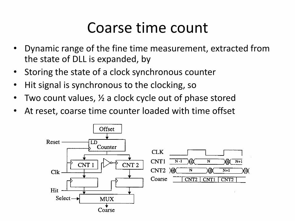
Coarse time count • Dynamic range of the fine time measurement, extracted from
the state of DLL is expanded, by
• Storing the state of a clock synchronous counter
• Hit signal is synchronous to the clocking, so
• Two count values, ½ a clock cycle out of phase stored
• At reset, coarse time counter loaded with time offset

y = 10.2397x - 120.8717R² = 1.0000
-1.2
-0.7
-0.2
0.3
0.8
0
2000
4000
6000
8000
10000
12000
0 200 400 600 800 1000 1200
Dev
iati
on
in n
s
HP
TDC
Co
un
ts
Delay in ns
CALIBRATION OF HPTDC CH0RESOLUTION OF HPTDC 98ps
DELAY STEP 25ns
CH0
Deviation from
Straight Line(ns)
(1/Slope) = resolution
RMS of Deviation ≈ 30
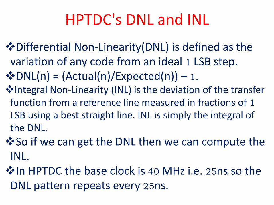
Differential Non-Linearity(DNL) is defined as the variation of any code from an ideal 1 LSB step. DNL(n) = (Actual(n)/Expected(n)) – 1. Integral Non-Linearity (INL) is the deviation of the transfer
function from a reference line measured in fractions of 1
LSB using a best straight line. INL is simply the integral of the DNL.
So if we can get the DNL then we can compute the INL. In HPTDC the base clock is 40 MHz i.e. 25ns so the DNL pattern repeats every 25ns.
HPTDC's DNL and INL

HPTDC's DNL test result
-0.4
-0.2
0
0.2
0.4
0.6
0.8
1
1.2
1.4
0 50 100 150 200 250 300
DN
L
Bins(1 bin=98ps)
At 98ps the DNL is +1.25 bin to -0.1 bin

HPTDC's INL test result
-3.5
-3
-2.5
-2
-1.5
-1
-0.5
0
0.5
1
0 50 100 150 200 250 300
INL
Bins(1 bin=98ps)
At 98ps the INL is -2.5 bin to +0.5 bin

Test Condition Effective resolution (RMS)
98ps resolution 64ps
98ps resolution after INL correction
34ps
24ps resolution 58ps
24ps resolution after INL correction
17ps
HPTDC's DNL/INL data correction • The fixed pattern in the INL is caused by 40 MHz cross talk from the logic
part of the chip to the time measurement part .
• As this crosstalk comes from the 40MHz clock, which is also the time reference of the TDC, the integral non linearity have a stable shape between chips and can therefore be compensated for using the LSB bits of the measurements.
232

LECTURE-22 December 28, 2012

234

235

236

MCA Vs MCS
MCA
• Multi Channel Analyser
• Uses ADC
• Sorts incoming pulses according to their pulse heights
• Channel represent pulse height
• Total channels Conversion gain
• Application: Spectroscopy
MCS
• Multi Channel Scaler
• Uses comparator and counter
• Counts incident pulse signals (regardless of amplitude) for a certain dwell time
• Channels represent bins in time
• Application: Decay curves of radioactive isotopes
237


Functional block diagram of a MCA
239

Two gamma rays with energies of 1.17 and 1.33 MeV