basic computer organization and designcs.sch.ac.kr/arch/arch-00/chap5.pdf · basic computer...
TRANSCRIPT
Basic Computer Organization and Design
Computer Organization Computer Architectures Lab
1
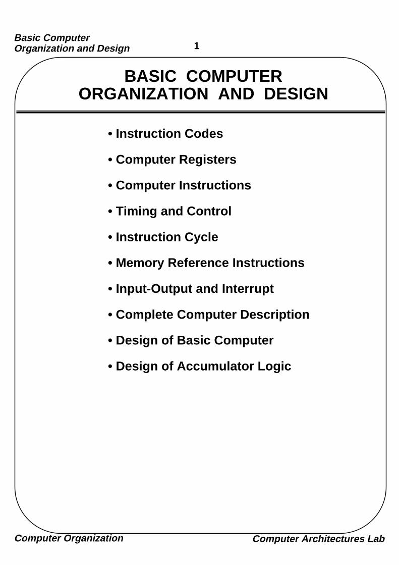
BASIC COMPUTERORGANIZATION AND DESIGN
• Instruction Codes
• Computer Registers
• Computer Instructions
• Timing and Control
• Instruction Cycle
• Memory Reference Instructions
• Input-Output and Interrupt
• Complete Computer Description
• Design of Basic Computer
• Design of Accumulator Logic

Basic Computer Organization and Design
Computer Organization Computer Architectures Lab
2
INSTRUCTION CODES
• Program: A set of instructions that specify the operations, operands, and the sequence by which processing has to occur.
• Instruction Code: A group of bits that tell the computer to perform a specific operation (a sequence of micro-operation) -->macro-operation
- usually divided into operation code, operand address, addressing mode, etc.- basic addressing modes Immediate, Direct, Indirect
Opcode Address
Instruction Format
Binary Operand
Instructions(program)
Operands(data)
Processor register(Accumulator, AC)
Memory4096x16
15 12 11 0
15 0
Instruction codes

Basic Computer Organization and Design
Computer Organization Computer Architectures Lab
3
INDIRECT ADDRESS
Effective Address(EFA, EA)The address, that can be directly used without modification to access an operand for a computation-type instruction, or as the target address for a branch-type instruction
Instruction codes
Opcode Address
Instruction Format
15 14 12 0
I
11
0 ADD 45722
Operand457
1 ADD 30035
1350300
Operand1350
+
AC
+
AC
Direct Address Indirect address

Basic Computer Organization and Design
Computer Organization Computer Architectures Lab
4
COMPUTER REGISTERS
List of BC Registers
DR 16 Data Register Holds memory operandAR 12 Address Register Holds address for memoryAC 16 Accumulator Processor registerIR 16 Instruction Register Holds instruction codePC 12 Program Counter Holds address of instructionTR 16 Temporary Register Holds temporary dataINPR 8 Input Register Holds input characterOUTR 8 Output Register Holds output character
Registers
Registers in the Basic Computer
11 0
PC
15 0
IR
15 0
TR
7 0
OUTR
15 0
DR
15 0
AC
11 0
AR
INPR0 7
Memory
4096 x 16

Basic Computer Organization and Design
Computer Organization Computer Architectures Lab
5
COMMON BUS SYSTEM
S2S1S0
Bus
Memory unit4096 x 16
LD INR CLR
Address
ReadWrite
AR
LD INR CLR
PC
LD INR CLR
DR
LD INR CLR
ACAdderandlogic
E
INPR
IR
LD
LD INR CLR
TR
OUTR
LDClock
16-bit common bus
7
1
2
3
4
5
6
Registers

Basic Computer Organization and Design
Computer Organization Computer Architectures Lab
6
COMPUTER(BC) INSTRUCTIONS
Basic Computer Instruction code format
Instructions
15 14 12 11 0I Opcode Address
(OP-code = 000 ~ 110)Memory-Reference Instructions
15 12 11 0Register operation
(OP-code = 111, I = 0)Register-Reference Instructions
15 12 11 0I/O operation
(OP-code =111, I = 1) Input-Output Instructions
0 1 1 1
1 1 1 1
Basic Computer Organization and Design
Computer Organization Computer Architectures Lab
7
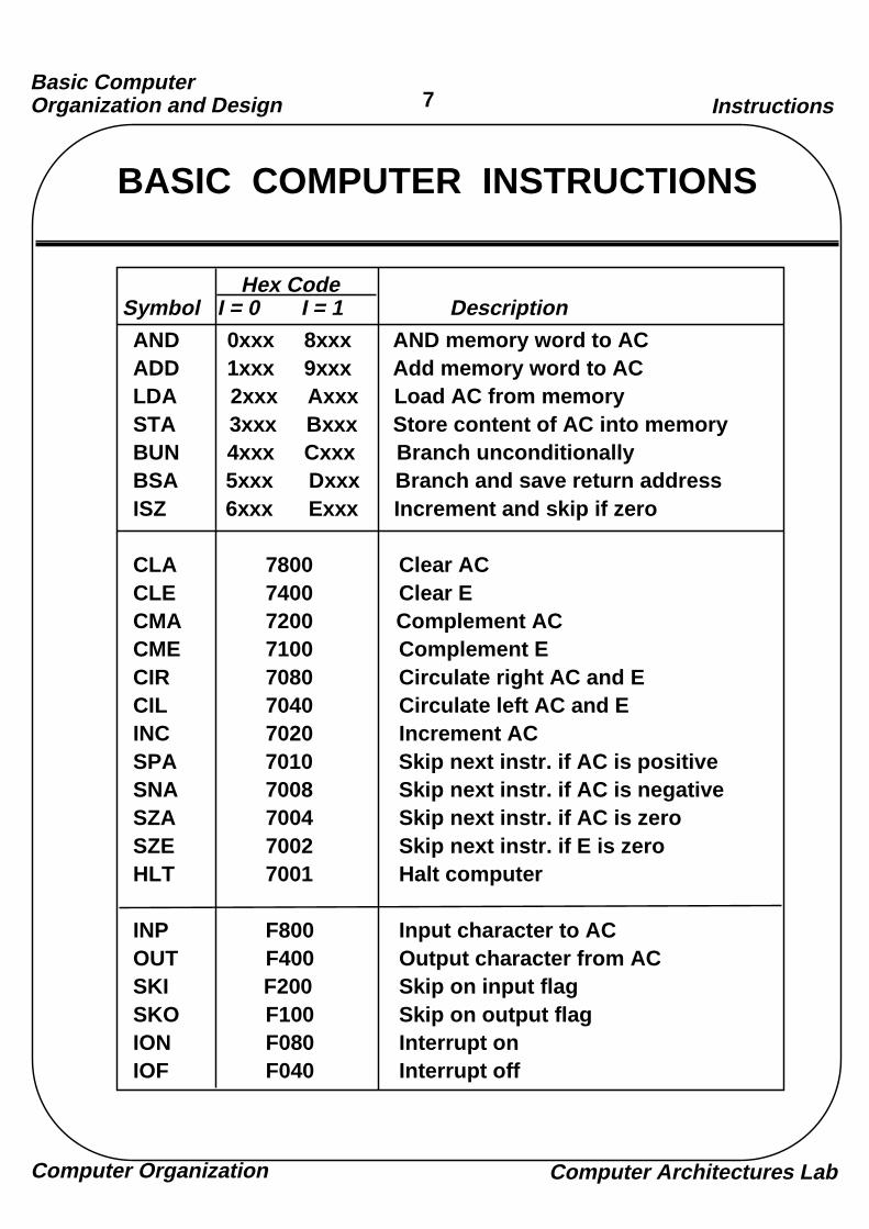
BASIC COMPUTER INSTRUCTIONS
Hex CodeSymbol I = 0 I = 1 DescriptionAND 0xxx 8xxx AND memory word to ACADD 1xxx 9xxx Add memory word to ACLDA 2xxx Axxx Load AC from memorySTA 3xxx Bxxx Store content of AC into memoryBUN 4xxx Cxxx Branch unconditionallyBSA 5xxx Dxxx Branch and save return addressISZ 6xxx Exxx Increment and skip if zero
CLA 7800 Clear ACCLE 7400 Clear ECMA 7200 Complement ACCME 7100 Complement ECIR 7080 Circulate right AC and ECIL 7040 Circulate left AC and EINC 7020 Increment ACSPA 7010 Skip next instr. if AC is positiveSNA 7008 Skip next instr. if AC is negativeSZA 7004 Skip next instr. if AC is zeroSZE 7002 Skip next instr. if E is zeroHLT 7001 Halt computer
INP F800 Input character to ACOUT F400 Output character from ACSKI F200 Skip on input flagSKO F100 Skip on output flagION F080 Interrupt onIOF F040 Interrupt off
Instructions
Basic Computer Organization and Design
Computer Organization Computer Architectures Lab
8
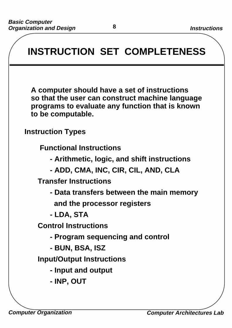
INSTRUCTION SET COMPLETENESS
Instruction Types
A computer should have a set of instructions so that the user can construct machine language programs to evaluate any function that is known to be computable.
Functional Instructions
- Arithmetic, logic, and shift instructions
- ADD, CMA, INC, CIR, CIL, AND, CLA
Transfer Instructions
- Data transfers between the main memory
and the processor registers
- LDA, STA
Control Instructions
- Program sequencing and control
- BUN, BSA, ISZ
Input/Output Instructions
- Input and output
- INP, OUT
Instructions

Basic Computer Organization and Design
Computer Organization Computer Architectures Lab
9
TIMING AND CONTROL
Control unit implementation
Control unit of basic computer
Hardwired Implementation
Microprogrammed Implementation
Instruction register (IR)15 14 13 12 11 - 0
3 x 8decoder
7 6 5 4 3 2 1 0
Controllogicgates
ID0
15 14 . . . 2 1 04 x 16
decoder
4-bitsequence
counter(SC)
Increment (INR)Clear (CLR)
Clock
Other inputs
Controloutputs
D
T
T
7
15
0
Timing and control

Basic Computer Organization and Design
Computer Organization Computer Architectures Lab
10
TIMING SIGNALS
ClockT0 T1 T2 T3 T4 T0
T0
T1
T2
T3
T4
D3
CLR SC
- Generated by 4-bit sequence counter and 4x16 decoder- The SC can be incremented or cleared.
- Example: T0, T1, T2, T3, T4, T0, T1, . . . Assume: At time T4, SC is cleared to 0 if decoder output D3 is active.
D T : SC <- 03 4
Timing and control
Basic Computer Organization and Design
Computer Organization Computer Architectures Lab
11
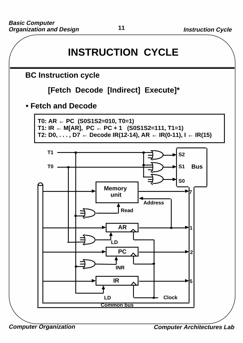
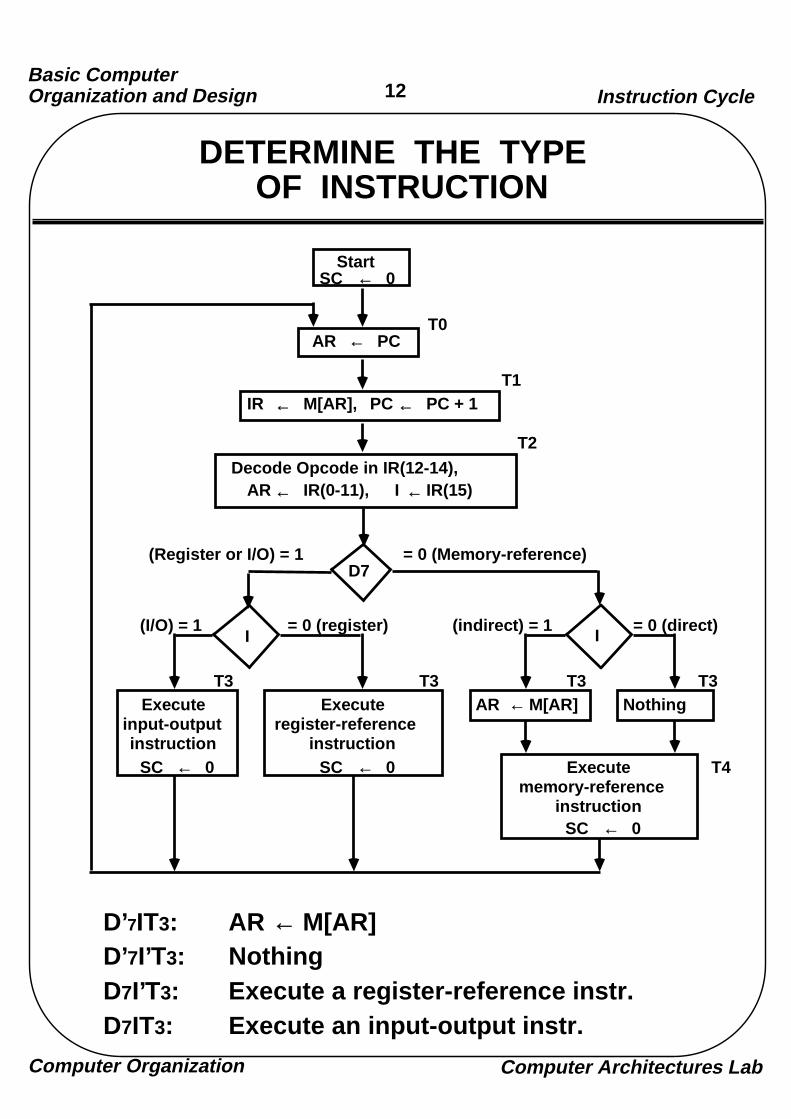
INSTRUCTION CYCLE
BC Instruction cycle
[Fetch Decode [Indirect] Execute]*
• Fetch and Decode
T0: AR ← PC (S0S1S2=010, T0=1)T1: IR ← M[AR], PC ← PC + 1 (S0S1S2=111, T1=1)T2: D0, . . . , D7 ← Decode IR(12-14), AR ← IR(0-11), I ← IR(15)
S2
S1
S0
Bus
7Memory
unitAddress
Read
AR
LD
PC
INR
IR
LD Clock
1
2
5
Common bus
T1
T0
Instruction Cycle
Basic Computer Organization and Design
Computer Organization Computer Architectures Lab
12
DETERMINE THE TYPE OF INSTRUCTION
StartSC ← 0
AR ← PCT0
IR ← M[AR], PC ← PC + 1T1
AR ← IR(0-11), I ← IR(15)Decode Opcode in IR(12-14),
T2
D7= 0 (Memory-reference)(Register or I/O) = 1
II
Executeregister-reference
instructionSC ← 0
Executeinput-outputinstruction
SC ← 0
M[AR]←AR Nothing
= 0 (register)(I/O) = 1 = 0 (direct)(indirect) = 1
T3 T3 T3 T3
Executememory-reference
instructionSC ← 0
D’7IT3: AR ← M[AR]D’7I’T3: NothingD7I’T3: Execute a register-reference instr.D7IT3: Execute an input-output instr.
Instruction Cycle
T4

Basic Computer Organization and Design
Computer Organization Computer Architectures Lab
13
REGISTER REFERENCE INSTRUCTIONS
r = D I’ T => Register Reference InstructionBi = IR(i) , i=0,1,2,...,11
7
- D = 1, I = 0- Register Ref. Instr. is specified in b0 ~ b11 of IR Transferred to AR during T2
7
- Execution starts with timing signal T3
Instruction Cycle
Register Reference Instructions are identified when
CLA rB : AC <- 0CLE rB : E <- 0CMA rB : AC <- ACCME rB : E <- ECIR rB : AC <-CIL rB : AC <- shl AC, AC(0) <- E, E <- AC(15)INC rB : AC <- AC + 1SPA rB : If (AC(15) = 0) then (PC <- PC + 1) SNA rB : If (AC(15) = 1) then (PC <- PC + 1) SZA rB : If (AC = 0) then (PC <- PC + 1) SZE rB : If (E = 0) then (PC <- PC + 1) HLT rB : S <- 0 (S is a start-stop flip-flop)
11
10
9
87
6
5
4
32
1
0
shr AC, AC(15) <- E, E <- AC(0)
r SC <− 0
3
Basic Computer Organization and Design
Computer Organization Computer Architectures Lab
14
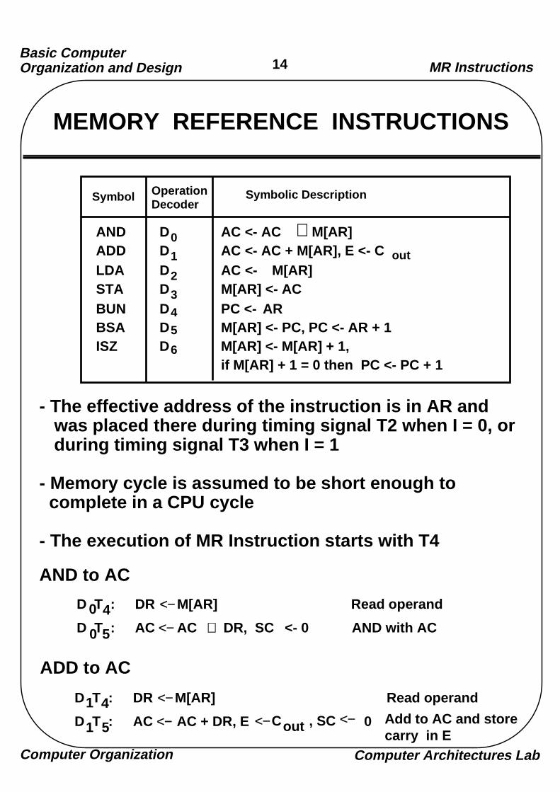
MEMORY REFERENCE INSTRUCTIONS
AND to AC
ADD to AC
- The effective address of the instruction is in AR and was placed there during timing signal T2 when I = 0, or during timing signal T3 when I = 1
- Memory cycle is assumed to be short enough to complete in a CPU cycle
- The execution of MR Instruction starts with T4
D T : DR <− M[AR] Read operand
D T : AC <− AC ∧ DR, SC <- 0 AND with AC0 4
0 5
D T : DR <− M[AR] Read operand
D T : AC <− AC + DR, E <− 0 Add to AC and storecarry in E
1 4
1 5 C out , SC <−
MR Instructions
Symbol OperationDecoder
Symbolic Description
AND D AC <- AC ∧ M[AR]ADD D AC <- AC + M[AR], E <- C outLDA D AC <- M[AR]STA D M[AR] <- ACBUN D PC <- ARBSA D M[AR] <- PC, PC <- AR + 1ISZ D M[AR] <- M[AR] + 1,
if M[AR] + 1 = 0 then PC <- PC + 1
0
1
2
3
4
5
6
Basic Computer Organization and Design
Computer Organization Computer Architectures Lab
15
MEMORY REFERENCEINSTRUCTIONS
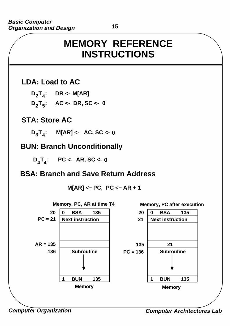
LDA: Load to AC
STA: Store AC
BUN: Branch Unconditionally
BSA: Branch and Save Return Address
M[AR] <− PC, PC <− AR + 1
21
D T : DR <- M[AR]
D T : AC <- DR, SC <- 02 4
2 5
D T : AC, SC <-M[AR] <-3 4 0
D T : AR, SC <-PC <-4 4 0
0 BSA 135Next instruction
Subroutine
20PC = 21
AR = 135
136
1 BUN 135
Memory, PC, AR at time T4
0 BSA 135Next instruction
Subroutine
2021
135
PC = 136
1 BUN 135
Memory, PC after execution
Memory Memory
Basic Computer Organization and Design
Computer Organization Computer Architectures Lab
16
MEMORY REFERENCEINSTRUCTIONS
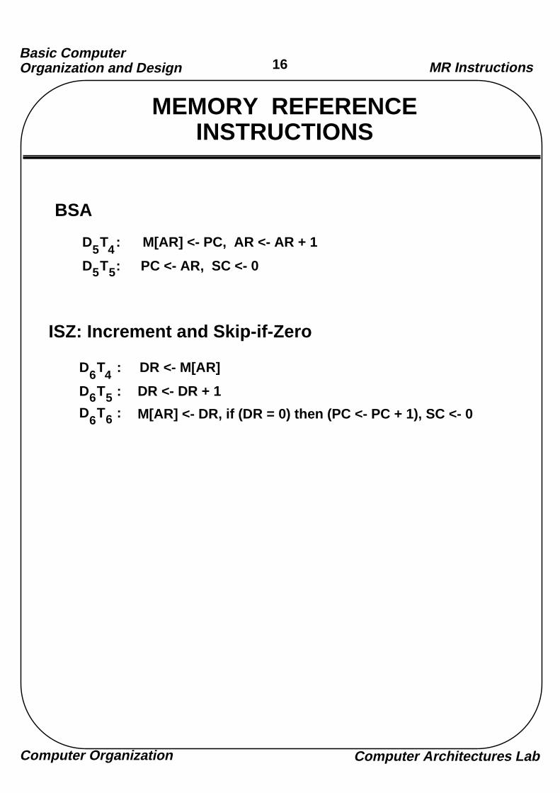
BSA
ISZ: Increment and Skip-if-Zero
MR Instructions
D T : M[AR] <- PC, AR <- AR + 1
D T : PC <- AR, SC <- 0 5 4
5 5
D T : DR <- M[AR]
D T : DR <- DR + 16 4
6 5D T : M[AR] <- DR, if (DR = 0) then (PC <- PC + 1), SC <- 06 6
Basic Computer Organization and Design
Computer Organization Computer Architectures Lab
17
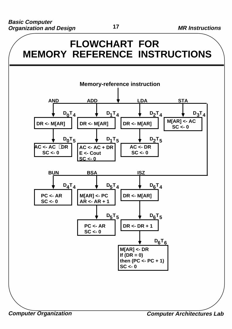
FLOWCHART FOR MEMORY REFERENCE INSTRUCTIONS
MR Instructions
Memory-reference instruction
DR <- M[AR] DR <- M[AR] DR <- M[AR] M[AR] <- ACSC <- 0
AND ADD LDA STA
AC <- AC DRSC <- 0
AC <- AC + DRE <- CoutSC <- 0
AC <- DRSC <- 0
D T0 4 D T1 4 D T2 4 D T3 4
D T0 5 D T1 5 D T2 5
PC <- ARSC <- 0
M[AR] <- PCAR <- AR + 1
DR <- M[AR]
BUN BSA ISZ
D T4 4 D T5 4 D T6 4
DR <- DR + 1
D T5 5 D T6 5
PC <- ARSC <- 0
M[AR] <- DRIf (DR = 0)then (PC <- PC + 1)SC <- 0
D T6 6
∧

Basic Computer Organization and Design
Computer Organization Computer Architectures Lab
18
INPUT-OUTPUT AND INTERRUPT
• Input-Output Configuration
INPR Input register - 8 bitsOUTR Output register - 8 bitsFGI Input flag - 1 bitFGO Output flag - 1 bitIEN Interrupt enable - 1 bit
- The terminal sends and receives serial information- The serial info. from the keyboard is shifted into INPR - The serial info. for the printer is stored in the OUTR- INPR and OUTR communicate with the terminal serially and with the AC in parallel.- The flags are needed to synchronize the timing difference between I/O device and the computer
A Terminal with a keyboard and a Printer
Input-outputterminal
Serialcommunication
interfaceComputer
registers and
flip-flops
Printer
Keyboard
Receiverinterface
Transmitterinterface
FGOOUTR
AC
INPR FGI
I/O and Interrupt
Serial Communications Path
Parallel Communications Path
Basic Computer Organization and Design
Computer Organization Computer Architectures Lab
19
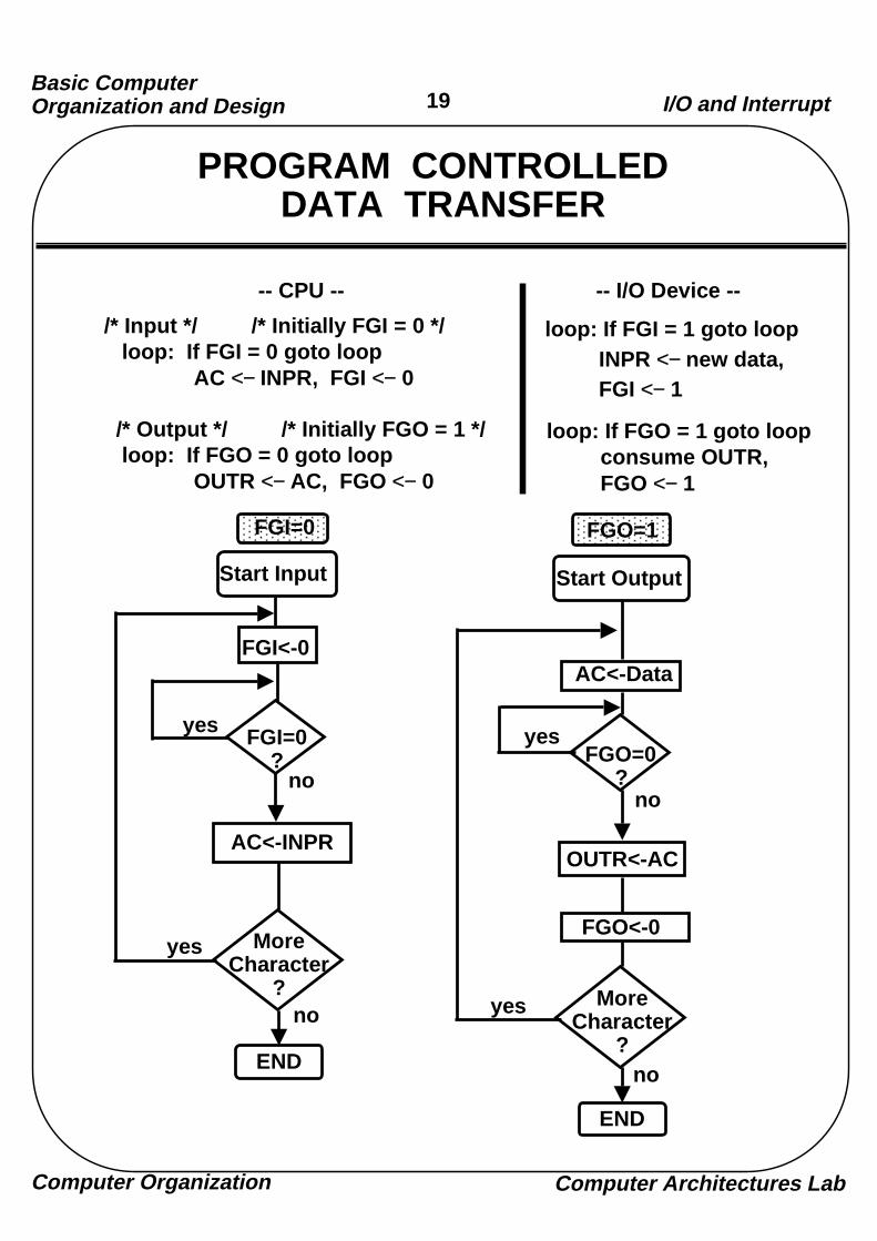
PROGRAM CONTROLLED DATA TRANSFER
loop: If FGI = 1 goto loop INPR <− new data, FGI <− 1 loop: If FGO = 1 goto loop consume OUTR, FGO <− 1
-- CPU -- -- I/O Device --
/* Input */ /* Initially FGI = 0 */ loop: If FGI = 0 goto loop AC <− INPR, FGI <− 0
/* Output */ /* Initially FGO = 1 */ loop: If FGO = 0 goto loop OUTR <− AC, FGO <− 0
I/O and Interrupt
Start Input
FGI<-0
FGI=0 ?
AC<-INPR
MoreCharacter
?
END
Start Output
FGO<-0
FGO=0 ?
MoreCharacter
?
END
OUTR<-AC
AC<-Data
yes
no
yes
no
FGI=0 FGO=1
yes
yesno
no
Basic Computer Organization and Design
Computer Organization Computer Architectures Lab
20
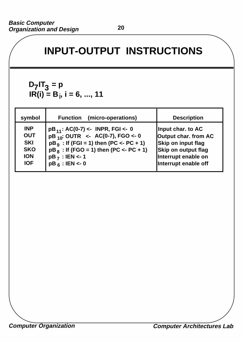
INPUT-OUTPUT INSTRUCTIONS
symbol DescriptionFunction (micro-operations)
D IT = p7IR(i) = B , i = 6, ..., 11
3i
INP Input char. to AC pB : AC(0-7) <- INPR, FGI <- 0OUT Output char. from AC pB : OUTR <- AC(0-7), FGO <- 0SKI Skip on input flag pB : If (FGI = 1) then (PC <- PC + 1) SKO Skip on output flag pB : If (FGO = 1) then (PC <- PC + 1) ION Interrupt enable on pB : IEN <- 1 IOF Interrupt enable off pB : IEN <- 0
11109876

Basic Computer Organization and Design
Computer Organization Computer Architectures Lab
21
PROGRAM-CONTROLLED INPUT/OUTPUT
• Program-controlled I/O
- Continuous CPU involvement I/O takes valuable CPU time- CPU slowed down to I/O speed- Simple- Least hardware
I/O and Interrupt
Input
LOOP, SKI DEV BUN LOOP INP DEV
Output
LOOP, LD DATA LOP, SKO DEV BUN LOP OUT DEV

Basic Computer Organization and Design
Computer Organization Computer Architectures Lab
22
INTERRUPT INITIATEDINPUT/OUTPUT
- Open communication only when some data has to be passed --> interrupt.
- The I/O interface, instead of the CPU, monitors the I/O device.
- When the interface founds that the I/O device is ready for data transfer, it generates an interrupt request to the CPU
- Upon detecting an interrupt, the CPU stops momentarily the task it is doing, branches to the service routine to process the data transfer, and then returns to the task it was performing.
* IEN (Interrupt-enable flip-flop)
- can be set and cleared by instructions- when cleared, the computer cannot be interrupted

Basic Computer Organization and Design
Computer Organization Computer Architectures Lab
23
FLOWCHART FOR INTERRUPT CYCLE
R = Interrupt f/f
- The interrupt cycle is a HW implementation of a branch and save return address operation.
- At the beginning of the next instruction cycle, the instruction that is read from memory is in address 1.
- At memory address 1, the programmer must store a branch instruction that sends the control to an interrupt service routine
- The instruction that returns the control to the original program is "indirect BUN 0"
I/O and Interrupt
R =1=0
Store return addressin location 0M[0] <- PC
Branch to location 1PC <- 1
IEN <- 0 R <- 0
Interrupt cycleInstruction cycle
Fetch and decodeinstructions
IEN
FGI
FGO
Executeinstructions
R <- 1
=1
=1
=1
=0
=0
=0

Basic Computer Organization and Design
Computer Organization Computer Architectures Lab
24
REGISTER TRANSFER OPERATIONS ININTERRUPT CYCLE
Register Transfer Statements for Interrupt Cycle
- R F/F <- 1 if IEN (FGI + FGO)T0’T1’T2’ => T0’T1’T2’ (IEN)(FGI + FGO): R <- 1
- The fetch and decode phases of the instruction cycle must be modified:
Replace T 0, T1, T2 with R'T 0, R'T1, R'T2
- The interrupt cycle :
RT0: AR <- 0, TR <- PCRT1: M[AR] <- TR, PC <- 0RT2: PC <- PC + 1, IEN <- 0, R <- 0, SC <- 0
0 BUN 112001
PC = 256255
1 BUN 0
Before interrupt
MainProgram
1120I/O
Program
0 BUN 11200
PC = 1
256255
1 BUN 0
After interrupt cycle
Memory
MainProgram
1120I/O
Program
256
I/O and Interrupt

Basic Computer Organization and Design
Computer Organization Computer Architectures Lab
25
FURTHER QUESTIONS ONINTERRUPT
Questions on Interrupt
How can the CPU recognize the device requesting an interrupt ?
Since different devices are likely to require different interrupt service routines, how can the CPU obtain the starting address of the appropriate routine in each case ?
Should any device be allowed to interrupt the CPU while another interrupt is being serviced ?
How can the situation be handled when two or more interrupt requests occur simultaneously ?
I/O and Interrupt

Basic Computer Organization and Design
Computer Organization Computer Architectures Lab
26
COMPLETE COMPUTER DESCRIPTIONFlowchart of Operations
Description
startSC <- 0, IEN <- 0, R <- 0
R
AR <- PCR’T0
IR <- M[AR], PC <- PC + 1
R’T1
AR <- IR(0~11), I <- IR(15)D0...D7 <- Decode IR(12 ~ 14)
R’T2
AR <- 0, TR <- PCRT0
M[AR] <- TR, PC <- 0RT1
PC <- PC + 1, IEN <- 0R <- 0, SC <- 0
RT2
D7
I I
ExecuteI/O
Instruction
ExecuteRR
Instruction
AR <- M[AR] Idle
D7IT3 D7I’T3 D7’IT3 D7’I’T3
ExecuteMR
Instruction
=0(Instruction =1(Interrupt Cycle) Cycle)
=1(Register or I/O) =0(Memory Ref)
=1 (I/O) =0 (Register) =1(Indir) =0(Dir)
D7’T4
Basic Computer Organization and Design
Computer Organization Computer Architectures Lab
27
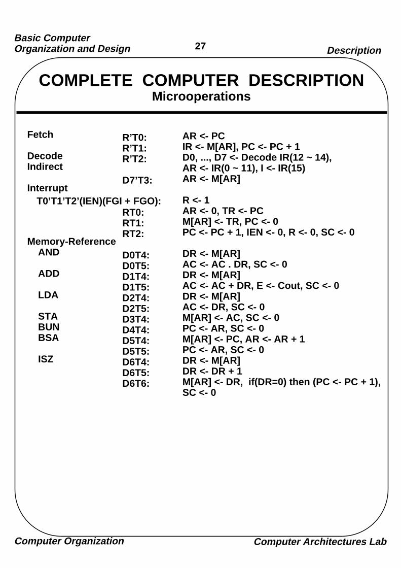
COMPLETE COMPUTER DESCRIPTIONMicrooperations
Description
Fetch
DecodeIndirect
Interrupt
Memory-Reference AND
ADD
LDA
STA BUN BSA
ISZ
R’T0:R’T1:R’T2:
D7’T3:
RT0:RT1:RT2:
D0T4:D0T5:D1T4:D1T5:D2T4:D2T5:D3T4:D4T4:D5T4:D5T5:D6T4:D6T5:D6T6:
AR <- PCIR <- M[AR], PC <- PC + 1D0, ..., D7 <- Decode IR(12 ~ 14), AR <- IR(0 ~ 11), I <- IR(15)AR <- M[AR]
R <- 1AR <- 0, TR <- PCM[AR] <- TR, PC <- 0PC <- PC + 1, IEN <- 0, R <- 0, SC <- 0
DR <- M[AR]AC <- AC . DR, SC <- 0DR <- M[AR]AC <- AC + DR, E <- Cout, SC <- 0DR <- M[AR]AC <- DR, SC <- 0M[AR] <- AC, SC <- 0PC <- AR, SC <- 0M[AR] <- PC, AR <- AR + 1PC <- AR, SC <- 0DR <- M[AR]DR <- DR + 1M[AR] <- DR, if(DR=0) then (PC <- PC + 1), SC <- 0
T0’T1’T2’(IEN)(FGI + FGO):

Basic Computer Organization and Design
Computer Organization Computer Architectures Lab
28
Register-Reference
CLA CLE CMA CME CIR CIL INC SPA SNA SZA SZE HLT
Input-Output
INP OUT SKI SKO ION IOF
D7I’T3 = rIR(i) = Bi r:rB11:rB10: rB9: rB8: rB7: rB6: rB5: rB4: rB3: rB2: rB1: rB0:
D7IT3 = p IR(i) = Bi p:pB11:pB10: pB9: pB8: pB7: pB6:
(Common to all register-reference instr)(i = 0,1,2, ..., 11)SC <- 0AC <- 0E <- 0AC <- AC’E <- E’AC <- shr AC, AC(15) <- E, E <- AC(0)AC <- shl AC, AC(0) <- E, E <- AC(15)AC <- AC + 1If(AC(15) =0) then (PC <- PC + 1)If(AC(15) =1) then (PC <- PC + 1)If(AC = 0) then (PC <- PC + 1)If(E=0) then (PC <- PC + 1)S <- 0
(Common to all input-output instructions)(i = 6,7,8,9,10,11)SC <- 0AC(0-7) <- INPR, FGI <- 0OUTR <- AC(0-7), FGO <- 0If(FGI=1) then (PC <- PC + 1)If(FGO=1) then (PC <- PC + 1)IEN <- 1IEN <- 0
COMPLETE COMPUTER DESCRIPTIONMicrooperations
Description

Basic Computer Organization and Design
Computer Organization Computer Architectures Lab
29
DESIGN OF BASIC COMPUTER(BC)
Hardware Components of BC
A memory unit: 4096 x 16.Registers: AR, PC, DR, AC, IR, TR, OUTR, INPR, and SCFlip-Flops(Status): I, S, E, R, IEN, FGI, and FGODecoders: a 3x8 Opcode decoder a 4x16 timing decoderCommon bus: 16 bitsControl logic gatesAdder and Logic circuit: Connected to AC
Control Logic Gates
- Input Controls of the nine registers
- Read and Write Controls of memory
- Set, Clear, or Complement Controls
of the flip-flops
- S2, S1, S0 Controls to select a register
for the bus
- AC, and Adder and Logic circuit
Design of Basic Computer

Basic Computer Organization and Design
Computer Organization Computer Architectures Lab
30
CONTROL OF REGISTERS AND MEMORY
Scan all of the register transfer statements that change the content of AR:
LD(AR) = R’T0 + R’T2 + D’7IT3CLR(AR) = RT0INR(AR) = D5T4
AR
LD
INRCLR
Clock
To bus12
From bus12
D’I
TT
RTDT
7
32
0
4
Address Register; AR
R’T0: AR <- PC LD(AR)R’T2: AR <- IR(0-11) LD(AR)D’7IT3: AR <- M[AR] LD(AR)RT0: AR <- 0 CLR(AR)D5T4: AR <- AR + 1 INR(AR)
Design of Basic Computer
Basic Computer Organization and Design
Computer Organization Computer Architectures Lab
31
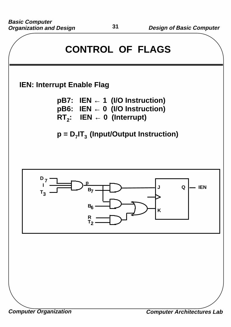
CONTROL OF FLAGS
pB7: IEN ← 1 (I/O Instruction)pB6: IEN ← 0 (I/O Instruction)RT2: IEN ← 0 (Interrupt)
p = D7IT3 (Input/Output Instruction)
IEN: Interrupt Enable Flag
DI
T3
7J
K
Q IENpB7
B6
T2R
Design of Basic Computer

Basic Computer Organization and Design
Computer Organization Computer Architectures Lab
32
CONTROL OF COMMON BUS
For AR
D4T4: PC ← ARD5T5: PC ← AR
x1 = D4T4 + D5T5
Design of Basic Computer
x1x2x3x4x5x6x7
Encoder
S2
S1
S0
Multiplexerbus select
inputs
x1 x2 x3 x4 x5 x6 x7 S2 S1 S0selectedregister
0 0 0 0 0 0 0 0 0 0 none1 0 0 0 0 0 0 0 0 1 AR0 1 0 0 0 0 0 0 1 0 PC0 0 1 0 0 0 0 0 1 1 DR0 0 0 1 0 0 0 1 0 0 AC0 0 0 0 1 0 0 1 0 1 IR0 0 0 0 0 1 0 1 1 0 TR0 0 0 0 0 0 1 1 1 1 Memory

Basic Computer Organization and Design
Computer Organization Computer Architectures Lab
33
DESIGN OF ACCUMULATOR LOGIC
Circuits associated with AC
All the statements that change the content of AC
16
16
8
Adder andlogic circuit
16 ACFrom DR
From INPR
Controlgates
LD INR CLR
16
To bus
Clock
D0T5: AC <- AC • DR AND with DRD1T5: AC <- AC + DR Add with DRD2T5: AC <- DR Transfer from DRpB 11: AC(0-7) <- INPR Transfer from INPRrB 9: AC <- AC ComplementrB 7: AC <- shr AC, AC(15) <- E Shift rightrB 6: AC <- shl AC, AC(0) <- E Shift leftrB 11: AC <- 0 ClearrB 5: AC <- AC + 1 Increment
Design of AC Logic
Basic Computer Organization and Design
Computer Organization Computer Architectures Lab
34
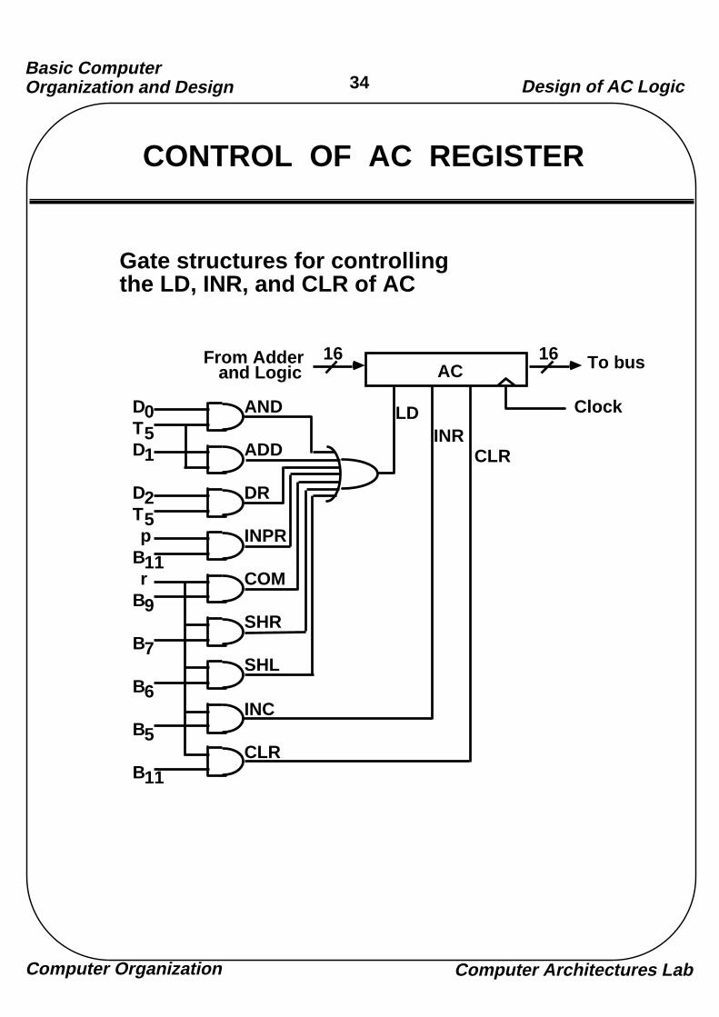
CONTROL OF AC REGISTER
Gate structures for controlling the LD, INR, and CLR of AC
AC
LDINR
CLR
Clock
To bus16From Adder and Logic
16
AND
ADD
DR
INPR
COM
SHR
SHL
INC
CLR
D0
D1
D2
B11
B9
B7
B6
B5
B11
r
p
T5
T5
Design of AC Logic

Basic Computer Organization and Design
Computer Organization Computer Architectures Lab
35
ADDER AND LOGIC CIRCUIT
One stage of Adder and Logic circuit
AND
ADD
DR
INPR
COM
SHR
SHL
J
K
QAC(i)
LD(Output of OR in Fig.5-20)
FA
C
C
FromINPRbit(i)
DR(i) AC(i)
AC(i+1)
AC(i-1)
i
i
i+1
I
Design of AC Logic