baseband response characterization of i-q modulators · baseband response characterization of i-q...
TRANSCRIPT
Baseband Response Characterization of I-Q Modulators Application Note
In modern wideband RF transmitters there are often modulation errors caused by the I-Q modulator section of the system which can significantly degrade the modulation quality. This application note provides a brief theory on the sources causing the modulation error and detailed steps of how to
characterize the I-Q modulator to correct for these errors. Learn how an arbitrary waveform generator (AWG) and a mixed domain oscilloscope (MDO) can be used for basedband frequency response, single-sideband suppression, amplitude and phase errors, and intermodulation performance.

Application Note
www.tektronix.com/application/rf-test2
Contents1 Introduction ...............................................................3
2 Overview of I-Q Modulation Theory ..........................3
3 Sources of Modulation Error .....................................43.1 Single-Side Band Suppression (SSBS) Test ...............5
3.1.1 Amplitude Error ..............................................53.1.2 Phase Error ....................................................5
3.2 Sideband Flatness (Conversion Gain Frequency Response) .................................................................6
4 Characterizing the I-Q Modulator .............................64.1 Sideband Flatness (Conversion Gain Frequency
Response) Measurement ...........................................74.1.1 Summary of Steps ..........................................9
4.2 Single-Sideband Suppression Measurement .............94.2.1 Summary of Steps ........................................10
4.3 OIP3 Measurement (Two-Tone Test).........................114.3.1 Summary of Steps ........................................12
5 Conclusion ...............................................................13
6 References ...............................................................13
www.tektronix.com/application/rf-test 3
Baseband Response Characterization of I-Q Modulators
1 - Introduction To modulate a signal there are three parameters available: amplitude, phase, and frequency which may be used separately or in combination to encode data. I-Q modulators use three input signals and are capable of generating any form of modulation such as AM, FM, and PM. I-Q modulators are commercially available in a variety of RF frequency ranges and are widely used in wireless and optical transmitters. Performance characterization and correction for deviating behavior of the modulator are key factors in ensuring a reliable wideband communication link. Supplying wideband baseband signals for the I and Q channels requires high performance DAC's whose response have been measured and corrected in order to use them as a basis for measuring the modulator's performance which is a challenging and time consuming step by itself. An arbitrary waveform generator (AWG) can be used to readily provide calibrated single-tone or wideband complex baseband signals to the I and Q baseband channels.
2 - Overview of I-Q Modulation TheoryThe mathematical basis for the complex quadrature modulation is the following well-known trigonometry identity:
Eq. 1
Where
Eq. 2
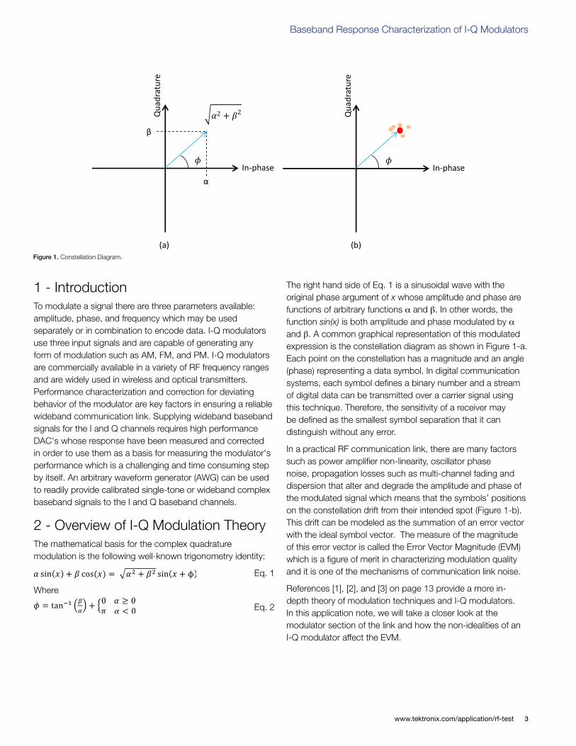
The right hand side of Eq. 1 is a sinusoidal wave with the original phase argument of x whose amplitude and phase are functions of arbitrary functions α and β. In other words, the function sin(x) is both amplitude and phase modulated by α and β. A common graphical representation of this modulated expression is the constellation diagram as shown in Figure 1-a. Each point on the constellation has a magnitude and an angle (phase) representing a data symbol. In digital communication systems, each symbol defines a binary number and a stream of digital data can be transmitted over a carrier signal using this technique. Therefore, the sensitivity of a receiver may be defined as the smallest symbol separation that it can distinguish without any error.
In a practical RF communication link, there are many factors such as power amplifier non-linearity, oscillator phase noise, propagation losses such as multi-channel fading and dispersion that alter and degrade the amplitude and phase of the modulated signal which means that the symbols’ positions on the constellation drift from their intended spot (Figure 1-b). This drift can be modeled as the summation of an error vector with the ideal symbol vector. The measure of the magnitude of this error vector is called the Error Vector Magnitude (EVM) which is a figure of merit in characterizing modulation quality and it is one of the mechanisms of communication link noise.
References [1], [2], and [3] on page 13 provide a more in-depth theory of modulation techniques and I-Q modulators. In this application note, we will take a closer look at the modulator section of the link and how the non-idealities of an I-Q modulator affect the EVM.
α
β
In-phaseQ
uadr
atur
eIn-phase
Qua
drat
ure
(a) (b)Figure 1. Constellation Diagram.
Application Note
www.tektronix.com/application/rf-test4
LO
I
Q
GBBI
GRF
GBBQ
GLOQ
GLOI
90°90°0°
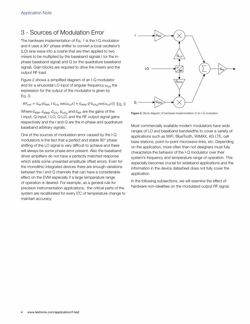
3 - Sources of Modulation ErrorThe hardware implementation of Eq. 1 is the I-Q modulator and it uses a 90° phase shifter to convert a local oscillator’s (LO) sine wave into a cosine that are then applied to two mixers to be multiplied by the baseband signals I (or the in-phase baseband signal) and Q (or the quadrature baseband signal). Gain blocks are required to drive the mixers and the output RF load.
Figure 2 shows a simplified diagram of an I-Q modulator and for a sinusoidal LO input of angular frequency the expression for the output of the modulator is given by Eq. 3:
Eq. 3
Where , , , and are the gains of the I-input, Q-input, I LO, Q LO, and the RF output signal gains respectively and the I and Q are the in-phase and quadrature baseband arbitrary signals.
One of the sources of modulation error caused by the I-Q modulators is the fact that a perfect and stable 90° phase shifting of the LO signal is very difficult to achieve and there will always be some phase error present. Also the baseband driver amplifiers do not have a perfectly matched response which adds some unwanted amplitude offset errors. Even for the monolithic integrated devices there are enough variations between the I and Q channels that can have a considerable effect on the EVM especially if a large temperature range of operation is desired. For example, as a general rule for precision instrumentation applications, the critical parts of the system are recalibrated for every 5˚C of temperature change to maintain accuracy.
Most commercially available modern modulators have wide ranges of LO and baseband bandwidths to cover a variety of applications such as WiFi, BlueTooth, WiMAX, 4G LTE, cell base stations, point-to-point microwave links, etc. Depending on the application, more often than not designers must fully characterize the behavior of the I-Q modulator over their system’s frequency and temperature range of operation. This especially becomes crucial for wideband applications and the information in the device datasheet does not fully cover the application.
In the following subsections, we will examine the effect of hardware non-idealities on the modulated output RF signal.
Figure 2. Block diagram of hardware implementation of an I-Q modulator.
www.tektronix.com/application/rf-test 5
Baseband Response Characterization of I-Q Modulators
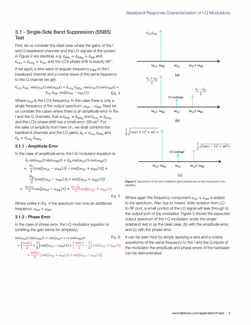
3.1 - Single-Side Band Suppression (SSBS) Test
First, let us consider the ideal case where the gains of the I and Q baseband channels and the LO signals of the system in Figure 2 are identical, e.g. and
, and the LO’s phase shift is exactly 90°.
If we apply a sine wave of angular frequency to the I baseband channel and a cosine wave of the same frequency to the Q channel we get:
Eq. 4
Where is the LO’s frequency. In this case there is only a single frequency in the output spectrum: . Next let us consider the cases where there is an amplitude error in the I and the Q channels, that is and , and the LO’s phase shift has a small error: (90+ )°. For the sake of simplicity from here on, we shall combine the baseband channels and the LO gains: and
.
3.1.1 - Amplitude Error
In the case of amplitude error, the I-Q modulator equation is:
Eq. 5
Where unlike in Eq. 4 the spectrum has now an additional frequency: .
3.1.2 - Phase Error
In the case of phase error, the I-Q modulator equation is (omitting the gain terms for simplicity):
Eq. 6
Where again the frequency component is added to the spectrum. Also due to mixers’ finite isolation from LO to RF port, a small portion of the LO signal will leak through to the output port of the modulator. Figure 3 shows the expected output spectrum of the I-Q modulator under the single-sideband test in (a) the ideal case, (b) with the amplitude error, and (c) with the phase error.
It can be seen how by simply applying a sine and a cosine waveforms of the same frequency to the I and the Q inputs of the modulator the amplitude and phase errors of the hardware can be demonstrated.
ωLO ωLO+ ωBBωLO- ωBB
LO Leakage
(b)
ωLO ωLO+ ωBBωLO- ωBB
LO Leakage
(c)
ωLO ωLO+ ωBBωLO- ωBB
(a)
Figure 3. Spectrums of the error sideband signal added due to the modulator’s non-idealities.

Application Note
www.tektronix.com/application/rf-test6
ωLOωLSB ωUSB
Ideal Sideband Response
Sideband Response Roll-Off
0° 90°+ (ω)
LO
I
Q
GI(ω)
GQ(ω)
GRF(ω)
3.2 – Sideband Flatness (Conversion Gain Frequency Response)
Another source of EVM error caused by the I-Q modulator is the unflatness of the baseband and the output RF amplifiers’ frequency response. For narrowband applications where only a few MHz of baseband bandwidth is desired, the flatness may not be a large contributor but for wideband applications beyond a few hundreds of MHz of modulation there usually would be a gain roll-off at higher frequency offsets from the LO frequency. Figure 4 shows an exaggerated example of a sideband response roll-off in the output RF spectrum.
Figure 5 shows a more realistic model of an I-Q modulator where the amplifiers are non-linear and have frequency dependent gain response. Also the LO phase shifter’s error is added to the ideal 90° phase shift.
4 - Characterizing the I-Q ModulatorIn the previous section we detailed the effects of hardware non-idealities on the output RF signal. Most I-Q modulator suppliers, among other parameters, provide key specifications such as single-sideband suppression, conversion gain, and output third-order intercept. But for wideband applications outside of the scope of the standard datasheet of the device or in the design cycle where the designer needs to iterate through a few adjustments to optimize the design having convenient and accurate measurement tools to test ideas and the device performance becomes increasingly important.
In this section we demonstrate how characteristics of a commercially available wideband I-Q modulator can be easily measured using Tektronix’s dual channel arbitrary waveform generator AWG70000 Series with sample rates up to 50 GS/s for the baseband signal generation along with the Tektronix RFXpress waveform generation software tool and the spectrum analyzer in Tektronix's MDO4104B-6 Mixed-Domain Oscilloscope with 6GHz of RF bandwidth on its' spectrum analyzer for the RF signal measurements. TI’s TRF370417 broadband I-Q modulator was used for the examples that follow.
Figure 4. Conversion gain frequency response.
Figure 5. Model of a practical I-Q modulator.

www.tektronix.com/application/rf-test 7
Baseband Response Characterization of I-Q Modulators
4.1 – Sideband Flatness (Conversion Gain Frequency Response) Measurement
This measurement is the same as a single mixer conversion gain measurement where the IF band is upconverted to the upper and lower sides of the LO frequency. Figure 6 shows the measurement set-up for the conversion gain measurement. Most commercially available modulators have balanced differential inputs for their I, Q, and LO inputs and the AWG’s channels conveniently provide calibrated differential outputs. To measure the I-channel conversion gain, AWG’s channel 1 is connected to the I input of the modulator and the Q-channel will remain unused but terminated to 50-Ω loads. The next step is applying a sine waveform to the baseband and the carrier LO inputs and measuring the double-sideband modulated RF output signal. There are several approaches to creating the full required set of the baseband sine waveforms including creating a series of waveforms using AWG’s built-in function generator or using some other external software tools such as RFXpress, MATLAB, Excel, etc. but the fastest way
is to generate a linear frequency modulation (chirp) that is a swept signal from the start frequency of the baseband BW to the end frequency of the baseband BW using the AWG and then monitoring the entire spectrum of the RF output from
to with the MDO’s spectrum analyzer in the Max Hold trace mode while the AWG loops through the chirp waveform. The MDO’s display will show two rapidly moving frequency spikes on either sides of the LO frequency that appear to sweep the spectrum while their peak values are being saved on the Max Hold trace. With the appropriate selection of the resolution bandwidth (RBW) on the MDO, almost the full spectrum can be captured and saved in a short time. It should be noted that lower RBW setting will provide a better resolution but it can take longer for the MDO to capture all the frequencies as its own acquisition band is also being internally swept for large spans. A good first estimate for the RBW is . For the Q-channel conversion gain measurement, the same step is performed as above but with the AWG connected to the Q input and the I input is terminated.
MDO4140-6
AWG70002
BBI BBQ
50Ω
LO
RFout
Ch. 1
RFXpress Software
50Ω
50Ω
Figure 6. Set-up for measuring the I-channel conversion gain over the entire baseband BW.
AWG70002A
MDO4104B-6

Application Note
www.tektronix.com/application/rf-test8
Figure 7 shows an example of the measured spectrum of the double-sideband modulation of the I-Q modulator under test with the LO at 4GHz. A waveform with linear frequency modulation from 1MHz to 1GHz was generated and loaded into the AWG to provide the I-channel baseband signal.
TIP: The RFXpress software’s RADAR pulse modulation section provides a convenient way to create and directly load the linear frequency modulation into the AWG.
To eliminate the cable loss and the AWG’s unflatness from the measurement, one of the AWG’s channel 1’s differential lines with the cable can be connected to the MDO’s RF input while the other line of channel 1 is terminated. Then the same chirp waveform can be played on the AWG and the same spectrum measurement approach as above can be performed to measure AWG plus cable frequency response. At the end, this loss should be factored in for the modulator’s conversion loss calculation. Figure 8 shows the simple setup where the amplitude frequency response of the AWG and cable can be characterized. For higher accuracy measurements, it is recommended that all of the modulator’s inputs have at least 3-dB attenuators to improve the VSWR to remove the unwanted small ripples in the frequency response measurements. This 3dB loss should be compensated for by the AWG and LO signal generator.
AWG70002
50Ω
MDO4140-6
Figure 7. Conversion gain frequency response measurement of the I-channel with the Max Hold trace. Carrier frequency: 4GHz at +8dBm input power with 1GHz of baseband. NOTE: a 6dB attenuator was added to the RF output of the I-Q modulator in this measurement.
Figure 9. AWG70002A's channel 1 and the cable’s amplitude frequency response measurement with the MDO using a linear chirp waveform from 1MHz to 1GHz.
Figure 8. Characterizing the AWG and cable's amplitude frequency response.
AWG70002A
MDO4104B-6

www.tektronix.com/application/rf-test 9
Baseband Response Characterization of I-Q Modulators
4.1.1 - Summary of Steps
1. Create a linear frequency modulated (chirp) waveform covering the entire baseband BW.
2. Load the chirp waveform to AWG’s channel 1.
3. Connect AWG’s channel 1 to the I input of the modulator and terminate the Q input.
4. Connect the LO signal with appropriate frequency and power level.
5. Connect the modlator’s RF output port to the MDO’s spectrum analyzer input port.
6. Set the MDO’s center frequency to the LO frequency.
7. Set the MDO’s span to .
8. Turn on the Max Hold trace on the MDO.
9. Adjust the RBW of the MDO to achieve a reasonably fast capture time but not so large that you sacrifice too much of the resolution. is a good first approximation.
10. Wait until the Max Hold trace has finished capturing the peak values of both modulation sidebands.
11. Connect AWG’s channel 1 to the Q inupt of the modulator and terminate the I input.
12. Repeat steps 4-10 to capture the Q-channel’s conversion loss response.
4.2 – Single-Sideband Suppression Measurement
As discussed in Section 3.1, to create a single-sideband modulated signal with suppressed carrier a sine and a cosine waveform of the same frequency are applied to the I and Q inputs respectively. This can easily be done with the AWG where the sine and cosine waveforms are generated using RFXpress or a third party software. Figure 10 shows the measurement setup for the SSBS measurement where the RFXpress is used to generate and load the baseband waveforms and the RF output spectrum is measured with the MDO.
MDO4140-6
AWG70002
BBI BBQ
50Ω
LO
RFout
Ch. 1 Ch. 2
RFXpress Software
DUT
Figure 10. SSBS measurement set-up.
AWG70002A
MDO4104B-6

Application Note
www.tektronix.com/application/rf-test10
For accurate measurements, phase matched cables should be used for the baseband signals and also all PCB traces leading to the device pins should be length matched. The phase mismatch between the I and Q paths of the measurement system can be corrected for with the AWG which offers independent phase control over its two channel with 0.5° steps. To measure the system’s phase mismatch, a sine wave of the frequency of interest and a copy of it with 180° phase shift can be generated by the RFXpress and loaded into AWG’s channel 1 and channel 2 respectively. The two channels can then be combined using a power splitter/combiner and measured with the MDO’s spectrum analyzer (Figure 12). The phase of either channel can be adjusted until the measured power of the combined wave is minimized. This should be done for all frequencies that are intended to be used for the SSBS measurements. For the phase correction, the required phase offset that was needed to minimize the power in this step should be added to the related channel of the AWG for the SSBS measurements. This process can also be programmed and automated using GPIB or TCPIP instrument control.
4.2.1 - Summary of Steps
1. Measure the I and Q path cables’ phase mismatch at every baseband frequency (Figure 12) and create a phase correction look-up table.
2. Generate a sine baseband waveform for channel 1 and a cosine baseband waveform for channel 2 of the AWG with applied phase mismatch correction measured in step 1.
3. Connect AWG’s channel 1 and channel 2 to the modulator’s I and Q inputs respectively.
4. Connect the LO signal with appropriate frequency and power level.
5. Connect the modulator's RF output port to the MDO’s spectrum analyzer input port.
6. Set the MDO’s center frequency to the LO frequency.
7. Set the MDO’s span to a value that covers both sidebands.
8. Use the delta feature of the trace markers to measure the power ratio of the LSB and the suppressed USB.
AWG70002
50Ω
MDO4140-6
50Ω
Splitter/Combiner
-6dB
Figure 11. Spectrum of the SSBS measurement with 500MHz of sideband modulation with 4GHz LO frequency at +8 dBm.
Figure 12. Phase calibration of the test system.
AWG70002A
MDO4104B-6

www.tektronix.com/application/rf-test 11
Baseband Response Characterization of I-Q Modulators
4.3 - OIP3 Measurement (Two-Tone Test)
The two-tone test to calculate the 3rd order intercept point is a measure of non-linearity of the device under test. The theory and details of this measurement technique have been discussed to a great detail in the reference material noted in [4] and [5] and many other freely available literature and here we only demonstrate how this test can be implemented using the AWG and the MDO and discuss their capabilities and limitations.
The third-order intermodulation (IM3) product measurement is a notoriously difficult and expensive measurement to make because it requires two isolated signal sources with a very high linearity and a spectrum analyzer with high dynamic range. Traditionally, generating the two signal tones for this measurement is done using two different RF signal sources with combined outputs and added attenuation to each generator for isolation improvements. With the ultra-high sample rate and excellent dynamic range of the AWG70000 series, it is possible to generate a single waveform that includes the two-tone signal for the baseband inputs of the I-Q modulator. The AWG70000 series with 50GS/s and
oversampling factor of 24 and using its DAC’s full range has an OIP3 of better than +26dBm up to 500MHz and better than +23dBm up to 800MHz. As a general rule to minimize the measurement error, the OIP3 of the measurement system should be at least 6dB or better than the OIP3 of the DUT. For example, in the AWG70000 series, this sets the limit to +20dBm of DUT OIP3 up to 500MHz.
Figure 13 shows the set-up for the OIP3 measurement where the RFXpress’s multi-carrier feature can be used to generate two tones in one channel. An MDO can be used to measure the RF spectrum. Figure 14 shows the baseband spectrum and the expected upper-side band RF spectrum of the modulator under the two-tone test.
To ensure that the MDO’s spectrum analyzer is not adding its own IM3 products, an external attenuator in addition to the MDO’s own internal attenuator should be used at the RF input but this raises the noise floor and the IM3 products can be lost in the noise. Lowering the RBW and also reducing the span to only cover one of the IM3 products can help alleviate this problem. Also while measuring the original tones the Auto Level should be used so that MDO would automatically adjust its internal attenuator setting.
MDO4140-6
AWG70002
BBI BBQ
50Ω
LO
RFout
Ch. 1
RFXpress Software
50Ω
50Ω
DUT
Att.
Figure 13. I-Q modulator OIP3 measurement set-up.
AWG70002A
MDO4104B-6

Application Note
www.tektronix.com/application/rf-test12
Figure 15 shows the measurement of the RF spectrum of the modulated two-tones and their IM3 products of the modulator used for the examples of this application note. The baseband center frequency is 500MHz. The calculated OIP3 based on measurements using Eq. 7 in this case is +10.3dBm which is about 16dB lower than the AWG’s OIP3.
Eq. 7
4.3.1 - Summary of Steps
1. Create a two-tone waveform with 1MHz separation and the center frequency at the desired baseband frequency.
2. Load the two-tone waveform to AWG’s channel 1.
3. Connect AWG’s channel 1 to the I input of the modulator and terminate the Q input.
4. Connect the LO signal with the appropriate frequency and power level.
5. Connect the modulator’s RF output port to MDO’s spectrum analyzer input port with an additional external attenuator that reduces the main tone levels to less than -20dBm.
6. Set the MDO’s center frequency to the LO frequency + the center frequency of the two tones.
7. Measure the power level of both tones and the relative power level of one of the IM3 products to its adjacent tone using the delta marker (Figure 14 and Figure 15).
8. Calculate the OIP3: .
BBI BBQ
LO
RFout50Ω
50Ω
DUT
Baseband Spectrum
RF Output Spectrum
fBBtone2fBB_tone1
BBtone1 BBtone2
fBB_center = (fBB_tone2+fBB_tone1)/2
fLO + fBB_center
ftone2ftone12ftone2 - ftone12ftone1 – ftone2
Ptone1 – PIM3_1
IM31 IM32
tone1 tone2
Figure 14. Baseband and the upper-side band RF spectrum of the I-Q modulator under two-tone test.
Figure 15. Spectrum of the modulated two test tones and their IM3 products. Two-tone test signals: 500MHz center frequency with 1MHz separation modulated by an I-Q modulator with the LO frequency of 4GHz at +8dBm.
www.tektronix.com/application/rf-test 13
Baseband Response Characterization of I-Q Modulators
5 ConclusionCharacterizing the non-ideal behaviors of the I-Q modulator in a communication system and correcting for them is key to having a reliable, wideband link. Tektronix’s arbitrary wave generator (AWG) along with RFXpress waveform generator software tool and multi-domain oscilloscope (MDO) can be used to provide a complete solution to measure critical characteristics of an I-Q modulator such as single-sideband suppression (SSBS), conversion loss frequency response, and the third-order intermodulation product (IM3). Utilizing the flexibility of the AWG and RFXpress to create linear frequency modulation along with the Max Hold feature of the MDO’s spectrum analyzer allows for fast and accurate frequency response measurements up to 6GHz. The AWG70000 series' state-of-the-art DAC and its exceptional high sample rate provides very linear output signals allowing for direct generation of baseband two-tones to be used for IM3 measurement suitable for most commercial applications with very high baseband bandwidths.
This powerful set of solution allows designers to characterize an I-Q modulator and easily and quickly iterate through necessary steps to optimize their design and achieve low EVM modulations in demanding wideband systems.
6 References[1] Rappaport, Theodore S. Wireless communications:
principles and practice. Vol. 2. New Jersey: Prentice Hall PTR, 1996.
[2] Chen, Sao-Jie, and Yong-Hsiang Hsieh. IQ calibration techniques for CMOS radio transceivers. Springer, 2006.
[3] Fischer, Walter. Digital video and audio broadcasting technology: a practical engineering guide. Springer, 2008.
[4] Golio, Mike, ed. The RF and microwave handbook. CRC press, 2010.
[5] Pozar, David M. Microwave engineering. Wiley. com, 2009.
For Further InformationTektronix maintains a comprehensive, constantly expanding collection of application notes, technical briefs and other resources to help engineers working on the cutting edge of technology. Please visit www.tektronix.com
Contact Tektronix:ASEAN / Australia (65) 6356 3900
Austria* 00800 2255 4835Balkans, Israel, South Africa and other ISE Countries +41 52 675 3777
Belgium* 00800 2255 4835Brazil +55 (11) 3759 7627Canada 1 (800) 833-9200
Central East Europe and the Baltics +41 52 675 3777Central Europe & Greece +41 52 675 3777
Denmark +45 80 88 1401Finland +41 52 675 3777
France* 00800 2255 4835Germany* 00800 2255 4835
Hong Kong 400-820-5835Ireland* 00800 2255 4835
India +91-80-30792600Italy* 00800 2255 4835
Japan 0120-441-046Luxembourg +41 52 675 3777
Macau 400-820-5835Mongolia 400-820-5835
Mexico, Central/South America & Caribbean 52 (55) 56 04 50 90Middle East, Asia and North Africa +41 52 675 3777
The Netherlands* 00800 2255 4835Norway 800 16098
People’s Republic of China 400-820-5835Poland +41 52 675 3777
Portugal 80 08 12370Puerto Rico 1 (800) 833-9200
Republic of Korea +822-6917-5000Russia +7 495 664 75 64
Singapore +65 6356-3900South Africa +27 11 206 8360
Spain* 00800 2255 4835Sweden* 00800 2255 4835
Switzerland* 00800 2255 4835Taiwan 886-2-2656-6688
United Kingdom* 00800 2255 4835USA 1 (800) 833-9200
* If the European phone number above is not accessible, please call +41 52 675 3777
Contact List Updated June 2013
Copyright © 2014, Tektronix. All rights reserved. Tektronix products are covered by U.S. and foreign patents, issued and pending. Information in this publication supersedes that in all previously published material. Specification and price change privileges reserved. TEKTRONIX and TEK are registered trademarks of Tektronix, Inc. All other trade names referenced are the service marks, trademarks or registered trademarks of their respective companies.
02/14 EA/WWW 37W-29553-1