baseband processor of multi-purpose rfid tag
TRANSCRIPT

BASEBAND PROCESSOR OF MULTI-PURPOSE
RFID TAG
A THESIS SUBMITTED IN PARALLEL FULFULMENT OF THE
REQUIREMENTS FOR THE DEGREE OF
Bachelor in Technology
In
Electronics and Communication Engineering
by
Srijeya Shilabhadra (107EC017)
And
Mohammed Yasser (107EC029)
Department of Electronics and Communication Engineering National Institute of Technology, Rourkela
2007-2011
ii | P a g e
BASEBAND PROCESSOR OF MULTI-PURPOSE
RFID TAG
A THESIS SUBMITTED IN PARALLEL FULFULMENT OF THE
REQUIREMENTS FOR THE DEGREE OF
Bachelor in Technology
In
Electronics and Communication Engineering
by
Srijeya Shilabhadra (107EC017)
And
Mohammed Yasser (107EC029)
Under the guidance of
Prof. D.P.Acharya
Department of Electronics and Communication Engineering National Institute of Technology, Rourkela
2007-2011

iii | P a g e
National Institute of Technology
Rourkela
CERTIFICATE
This is to certify that the thesis entitled “Baseband processor design of a
Multi-Purpose RFID Tag” submitted by Srijeya Shilabhadra (107EC017) and
Mohammed Yasser (107EC029) in partial fulfilment for the requirements
for the award of Bachelor of Technology Degree in Electronics and
Communication Engineering at National Institute of Technology, Rourkela
(Deemed University) is an authentic work carried out by them under my
supervision.
To the best of my knowledge, the matter embodied in the thesis has not
been submitted by any other University/Institute for the award of any
Degree or Diploma.
Date:
Prof. D.P.Acharya
Department of Electronics and
Communication Engineering

iv | P a g e
BASEBAND PROCESSOR
DESIGN OF A
MULTIPURPOSE RFID TAG

v | P a g e
Acknowledgement
We take this opportunity as a privilege to thank all individuals whose support and
guidance have helped us complete our project in this stipulated period of time.
First and foremost we would like to express our deepest gratitude to our Project
Supervisor Prof.Debiprasad Priyabrata Acharya, Department of Electronics and
Communication Engineering, for granting us the opportunity to work on such an
interesting topic. He has extended his invaluable support, guidance, motivation and
encouragement throughout the period of this work. His readiness for consultation at all
times, his educative comments, constructive criticism and inputs, his concern and
assistance even with practical things have been extremely helpful.
We are deeply indebted to Mr.Ayas Kanta Swain and Mr.Sushant Kumar Pattnaik of NIT
Rourkela for helping us out during the execution of our project.
Sincere thanks to all our friends, especially Anup Sarma and Rohit Jain, who have
patiently extended all sorts of help for accomplishing this undertaking.
Finally, a word of thanks to all of them who have been associated with us and directly or
indirectly helped us during this project.
Srijeya Shilabhadra Mohammed Yasser
107EC017 107EC029
vi | P a g e
INDEX
CHAPTER 1 : INTRODUCTION AND LI ............................................................................................... 2
1.1 WHAT IS RFID? ............................................................................................................. 3
1.2 APPLICATIONS OF RFID .................................................................................................. 3
1.3 TYPES OF RFID TAGS ....................................................................................................... 4
1.4 RFID STANDARDS ............................................................................................................. 4
1.5 PARTS OF AN RFID SYSTEM ........................................................................................... 5
1.6 WORKING OF AN RFID SYSTEM .................................................................................... 6
CHAPTER 2 : MODEL AND ARCHITECHTURE .................................................................................... 7
2.1 READER-TAG MODEL ...................................................................................................... 8
2.1.1 The Conventional Single-purpose tag ............................................................................ 8
2.1.2 Multipurpose Tag Environment...................................................................................... 8
2.1.3 Implementing the Multipurpose RFID Tag .................................................................... 9
2.1.4 Advantages of the Multipurpose tag over the single purpose tag ................................... 9
2.2 THE RFID ARCHITECTURE ............................................................................................ 10
CHAPTER 3 : DESIGN AND ANALYSIS TOOLS USED ........................................................................ 12
3.1 DESIGN TOOLS ................................................................................................................ 13
3.2 XILINX ............................................................................................................................... 13
3.3 MODELSIM ........................................................................................................................ 14
CHAPTER 4 : IMPLEMENTATION .................................................................................................... 15
4.1 GENERATION OF SINE WAVE IN XILINX .................................................................. 16
4.1.1 Sine wave generation using IP core .............................................................................. 16
4.1.2 Sine wave generation using Look Up tables (LUTs) .................................................... 16
4.2 READER TO TAG COMMUNICATION .......................................................................... 17
4.2.1 ASK Modulator ............................................................................................................ 17
4.2.2 ASK Demodulator ........................................................................................................ 19
4.3 TAG TO READER COMMUNICATION .......................................................................... 19

vii | P a g e
4.3.1 BPSK Modulator .......................................................................................................... 19
4.4 DECODER AND MEMORYa ............................................................................................ 21
CHAPTER 5 : RESULTS .................................................................................................................... 22
5.1 SINE WAVE GENERATED .............................................................................................. 23
5.2 ASK MODULATED WAVEFORM .................................................................................. 23
5.3 ASK DEMODULATION WAVEFORMS ......................................................................... 24
5.4 BPSK MODULATION ....................................................................................................... 25
5.5 WAVEFORMS OF THE BASEBAND PROCESSOR ...................................................... 26
CHAPTER 6 : CONCLUSION AND FUTURE WORK ........................................................................... 27
6.1 CONCLUSION ................................................................................................................... 28
6.2 FUTURE WORK ................................................................................................................ 28
References ..................................................................................................................................... 30

1 | P a g e
Abstract
Radio frequency identification has found ubiquitous usage in today‟s industry.
Object identification and tracking, supply chain management, anti-theft and fraud
systems are just some of the uses RFID tags find in today‟s market. As the RFID
technology competes with other technologies present in the market, a large amount
of research has been undertaken in order to optimize the performance and cost
factors of the readers and tags involved in the RFID system. Various
implementations on different devices such as ICs and CMOS System on Chip (Soc)
have been tried out. FPGAs are also being considered as a potential target device for
implementing RFID systems.
This project aims at the design of an FPGA implementable RFID Tag processor
design for the purpose of baseband signal processing. A new architecture has been
proposed and implemented for this processor. This architecture takes into
consideration the flexibility of the entire system with the help if independent sub
modules. Also, the suggested architecture has taken into consideration the creation of
an innovative single tag for multiple purposes which can interact with various types
of readers and convey the required information to each one of them. The RFID tag
has been designed in accordance to EPCglobal Class1 Generation2 standard for
operation in the range of 860-960 MHz in the air interface.
The design of the tag components has been done with the help of XILINX and the
verifications and analysis with ModelSim.

2 | P a g e
CHAPTER 1
INTRODUCTION
AND
LITERATURE REVIEW

3 | P a g e
1.1 WHAT IS RFID?
Radio-frequency identification (RFID) is a technology that uses communication via
electromagnetic waves to exchange data between a terminal and an electronic tag attached
to an object, for the purpose of identification and tracking. Used to gather identifying
information about an object, the main motivation of deploying RFID tags is similar to that
of magnetic strips and bar codes. RFID tags hold to their credit various advantages over the
other technologies. While technologies like the magnetic strip (employed in ATM and
credit cards) and bar codes require physical alignment or physical contact with their readers,
a RFID tag can be read at distances up to 10 meters from the reader [1]
. With improvements
in the reader technology like the introduction of time delay elements in the transmission
from tags, multiple tags can be sensed together by a single reader, thus further adding to the
superiority of this technology over others. The cost of these tags, though higher than other
technologies, lies in the range of a few cents[2]
, hence the deployment of these tags is an
also an inexpensive affair. Another point which adds to the usefulness of the RFID
technology is the availability of a various types of tags to suit individual applications.
Currently we have tags which operate totally on battery, some which have a back up source
for power yet harness energy from the environment and there some which are totally reliant
on the power form the reader for their functioning. With this variety comes the amount of
choice a user has to find a tag which fits the cause of his/her application. The various
international standards which exist for RFID applications make it easier for multiple
vendors to produce systems which adhere to the same specifications. Thus, the tag
portability is improved. It is for these numerous advantages that RFID tags have become
almost ubiquitous in today.
1.2 APPLICATIONS OF RFID
The RFID technology finds it use in a number of applications involving tracking and
identifying objects, humans or animals. Given below are some of the easily found, day to
day uses of RFID:
4 | P a g e
Inventory tracking and management
In traffic regulation, currently being used for e-tolling and issuing passes for public
transport.
Asset management and retail sales.
Product tracking
At NIT Rourkela, RFID tags are employed in student ID cards and library books for
the library book issuing system of the Biju Patnaik Central Library (BPCL).
1.3 TYPES OF RFID TAGS
Apart from their implementation, RFID tags are generally categorized on the basis of their
source of power into the following types:
Active
Semi-passive
Passive
Active and Semi-passive RFID tags use internal batteries to power their circuits. An active
tag also uses its battery to broadcast radio waves to a reader, whereas a semi-passive tag
relies on the reader to supply its power for broadcasting. Because these tags contain more
hardware than passive RFID tags, they are more expensive.
Passive RFID tags rely entirely on the reader as their power source. These tags are read up
to 10 meters away and have lower production costs, meaning that they can be applied to less
expensive merchandise.
1.4 RFID STANDARDS
For the purpose of achieving long distance detection the UHF RFID standard has been used
for the designing the tag. EPCglobal Class-I Genereation-2 [3]
standard is once such UHF
standard whose modifications like ISO/IEC 18000-6 Type C and type B [4] – [6]
standards are
defined for the frequency range of 860- 960 MHz for the air interface.
5 | P a g e
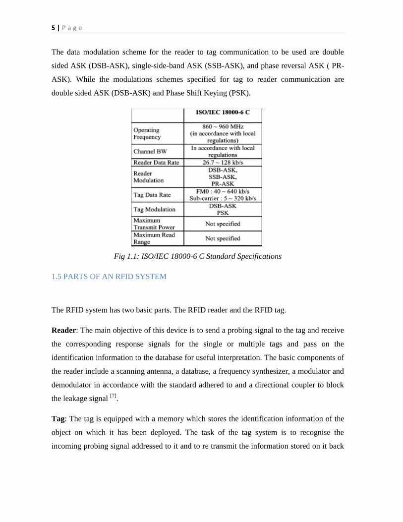
The data modulation scheme for the reader to tag communication to be used are double
sided ASK (DSB-ASK), single-side-band ASK (SSB-ASK), and phase reversal ASK ( PR-
ASK). While the modulations schemes specified for tag to reader communication are
double sided ASK (DSB-ASK) and Phase Shift Keying (PSK).
Fig 1.1: ISO/IEC 18000-6 C Standard Specifications
1.5 PARTS OF AN RFID SYSTEM
The RFID system has two basic parts. The RFID reader and the RFID tag.
Reader: The main objective of this device is to send a probing signal to the tag and receive
the corresponding response signals for the single or multiple tags and pass on the
identification information to the database for useful interpretation. The basic components of
the reader include a scanning antenna, a database, a frequency synthesizer, a modulator and
demodulator in accordance with the standard adhered to and a directional coupler to block
the leakage signal [7]
.
Tag: The tag is equipped with a memory which stores the identification information of the
object on which it has been deployed. The task of the tag system is to recognise the
incoming probing signal addressed to it and to re transmit the information stored on it back

6 | P a g e
to the reader. Depending on the type of tag the components it is comprised of may vary, but
tags generally contain an antenna, a modulator, a demodulator and a memory unit [8].
Fig 1.2: A RFID system
1.6 WORKING OF AN RFID SYSTEM
The tag contains the identification information and it is the task of the reader to retrieve it.
The readers modulator receives information from the database as to which tag is to be
accessed; this information is modulated on to a Continuous Wave (CW) and transmitted by
the antenna(s) of the reader [1]
. The tag receives the CW on its antenna, the power
harvesting circuits are then activated (in case of passive tags), the incoming signal is
demodulated and in accordance to that the necessary information from the tag is retrieved,
this information is then modulated on another CW and retransmitted back to the reader. The
readers demodulator receives this information and passes it on to the database after the
necessary processing. The database performs the necessary operations on the data received
and returns the useful information to the user.

7 | P a g e
CHAPTER 2
MODEL AND
ARCHITECTURE

8 | P a g e
2.1 READER-TAG MODEL
2.1.1 The Conventional Single-purpose tag
Normally the RFID tags that we encounter cater to a single purpose i.e. they contain a single
set of data for a particular purpose. When subjected to the probing signal, they send the
whole of the data to the reader. This simple sequence though pretty effective runs the risk of
data redundancy i.e. all the data sent to the reader might not be of use to it.
2.1.2 Multipurpose Tag Environment
Consider an environment with multiple readers which have to obtain different types of
information about a common object. One method of implementation is to deploy multiple
tags which interact with only one of the readers to provide the required information. In this
project we have considered the possibility of replacing these multiple number of tags with a
single tag capable of interacting with all the readers and providing the necessary
information in accordance with the probing signal of individual reader. In order to illustrate
this let us consider the implementation of a Universal Identification (UID) being currently
implemented by the Indian government [9]
.
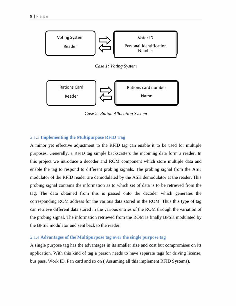
Let us consider that for this purpose every individual of India is given an identification card
which is equipped with an RFID tag. This tag has a memory element (implementation of
this shall be explained in the next section) which stores various data of an individual such as
name, address, contact number, voter ID number, passport number, pan card number etc.
Hence the current identification card can work as a medium of operation in various
scenarios like voting, ration allocation, tax payment etc. In an alternate scenario the person
would be require to produce an identity card specific to a purpose. Thus we see that by
using a memory enabled tag, we can perform the tasks required by multiple tags though a
single tag. Not only does is this a convenience to the person but it also relieves the database
of the RFID reader which can now obtain all the data necessary form a single tag rather than
having to retrieve the related information from the database after having received a single
identification information.
9 | P a g e
Case 1: Voting System
Case 2: Ration Allocation System
2.1.3 Implementing the Multipurpose RFID Tag
A minor yet effective adjustment to the RFID tag can enable it to be used for multiple
purposes. Generally, a RFID tag simple backscatters the incoming data form a reader. In
this project we introduce a decoder and ROM component which store multiple data and
enable the tag to respond to different probing signals. The probing signal from the ASK
modulator of the RFID reader are demodulated by the ASK demodulator at the reader. This
probing signal contains the information as to which set of data is to be retrieved from the
tag. The data obtained from this is passed onto the decoder which generates the
corresponding ROM address for the various data stored in the ROM. Thus this type of tag
can retrieve different data stored in the various entries of the ROM through the variation of
the probing signal. The information retrieved from the ROM is finally BPSK modulated by
the BPSK modulator and sent back to the reader.
2.1.4 Advantages of the Multipurpose tag over the single purpose tag
A single purpose tag has the advantages in its smaller size and cost but compromises on its
application. With this kind of tag a person needs to have separate tags for driving license,
bus pass, Work ID, Pan card and so on ( Assuming all this implement RFID Systems).
Voting System
Reader
Voter ID
Personal Identification Number
Rations Card
Reader
Rations card number
Name
Rations eligibility

10 | P a g e
As can be seen from the UID example of the tag can also be used for a multitude of
applications. So instead of needing multiple tags for various uses a user can have a single
tag which incorporates all the data from the various tags into a single one, with only the
relevant information being retrieved each time. This not only does away with the
inconvenience of carrying multiple IDs but also reduces the pressure on database systems
since majority of the user information is on the tag itself.
A drawback of this method is the increased cost that has to be incurred because of the extra
blocks that have been introduced (the ask demodulator, the decoder, increased memory).
2.2 THE RFID ARCHITECTURE
Conventional architectures such as the Neumann architecture or the Harvard architecture
can be used for optimizing performance and high speed, but in order to achieve a
multipurpose tag capable of interacting with multiple reader environments while taking the
power consumption into consideration [8]
, an innovative architecture for the baseband
processor has been suggested.
Fig 2.1: Adopted Architecture
The above given architecture formed the basis of our design. Some of the components
which were non-essential in our design were removed while the final architecture consisting

11 | P a g e
of 5 integral parts was adopted. The 5 components were the ASK modulator, decoder,
memory element, BPSK demodulator and a sine look up table. This above model gives
flexibility to the design as individual sub-modules can be altered independently without
affecting the system as a whole.
Fig 2.2: Implemented Architecture

12 | P a g e
CHAPTER 3
DESIGN AND ANALYSIS TOOLS
USED

13 | P a g e
3.1 DESIGN TOOLS
The architecture given above was described using VHDL. The XILINX 10.1 XST (Xilinx
Synthesis Technology) was used to synthesis the entire system for the Spartan 3E FPGA.
As analog signals cannot be viewed using the XILINX testbench, the outputs were viewed
in ModelSim, a simulation and debugging software from Mentor Graphics.
3.2 XILINX
XILINX is a design environment which consists of a set of programs which can be used to
capture, simulate and design digital systems which can be implemented on a FPGA (Field
Programmable Gate Array) or a CPLD (Complex Programmable Logic Device). It consists
of a GUI which enables the design using toolbars, menus and icons.
Given below are the steps involved in designing a system using XILINX
Fig: 3.1 Steps involved in design using XILINX [10]
Design Entry
This is the first step involved in the design and is done by creating source “Source” files.
Schematics or Hardware Description Languages (HDL) such as VHDL or Verilog can be
used for creating such files
Design Synthesis
The synthesis step involves the creation of netlist files from the various source files. These
files serve as input to the implementation module.

14 | P a g e
Design Verification (Simulation)
Simulators are used to test and verify the functionality, behaviour and timing of a circuit
designed. The various types of simulation are the functionality, behavioural and timing
simulations.
Design Implementation
After the generation of the netlist file, the implementation converts the logic design into a
physical file which can be „dumped‟ onto a device such as Virtex or Spartan FPGA.
Given below is a screenshot of a project navigator window of XILINX 10.1
3.3 MODELSIM
ModelSim is powerful HDL simulation and debugging tool which can be used to verify the
behavioral and timing simulation of a design. It can be used to observe the outputs and
internal signals of a module [11]
. A major advantage over XILINX and the main motivation
of using ModelSim in our work was the ability of observing analog waveforms such as that
of the modulation schemes used in this project.

15 | P a g e
CHAPTER 4
IMPLEMENTATION

16 | P a g e
4.1 GENERATION OF SINE WAVE IN XILINX
Generation of trigonometric waveforms on XILINX is of key importance since all the
modulation schemes used require the use of these functions. The modulation schemes
implemented in this project require the implementation of sine wave.
Primarily there are two methods for the implementation of sine wave in XILINX
i. Sine wave generation using IP core
ii. Sine wave generation using Look Up tables(LUTs)
4.1.1 Sine wave generation using IP core
Xilinx Intellectual Property (IP) Cores are key building blocks of Xilinx Targeted Design
Platforms. An extensive catalog of base-level cores is available to address the general needs
of FPGA designers, as well as robust domain- and market-specific cores to address
requirements found in DSP, Embedded, and Connectivity designs. Xilinx IP cores free up
precious time and resources one would normally spend developing standard functions and
helps us focus instead on the aspects of our design that differentiate our product from the
competition.
Xilinx Corporation distributes free and commercial Intellectual properties (IP) Cores for
FPGAs through its Core Generator System [12]
XILINX IP core library include those for the generation of sine and cosine functions. It
provides the programmer the option to choose the frequency of the sine wave.
This method was initially adopted. The ip core used was “c_sin_cos_v5.0_pack.vhd”.
This method was later discontinued as it required the manual compilation of various
modules of XILINXCoreLib Library each time the program had to be run.
4.1.2 Sine wave generation using Look Up tables (LUTs)
This is a more fundamental approach to the generation of sine wave. In this the various data
values are taken which when plotted against time give us a representation of the sine wave.
This is the method that has been adopted in this project. The various data values of the sine
wave might be obtained from MATLAB. The number of values taken to construct the sine

17 | P a g e
wave will determine its smoothness. Although more number of values will give a smoother
sine wave but the memory requirement would be more.
For our case the number of values to plot a single sine wave was taken to be 30.
t = 0 : (pi/15) : 2*pi ; % for 30 values
Then the sine values corresponding to these values of t were taken and scaled to the
resolution of 8 bits
sin(t)*10000/128
The above procedure yields 30 sine wave values as given below
0,16,31,45,58,67,74,77,77,74,67,58,45,31,16,0,-16,-31,-45,-58,-67,-74,-77,-77,-74,-67,-58,-
45,-31,-16
These values have been further multiplied by a factor 4 for better visualization in Modelsim,
thereby making each value of 10 bits.
Hence we have a sine wave which spans 30 clock cycles where two consecutive values of
the sine wave are separated by 1 clock cycle each.
4.2 READER TO TAG COMMUNICATION
The reader to tag communication plays an important part in this multi-purpose tag model.
Since the tag can be communicated to by a variety of readers which in turn can seek
different kinds of information, it is important that the tag differentiates between the various
readers. To ensure this, the probing signal sent by the reader contains information regarding
the information that is to be retrieved from the tag.
The reader to tag communication is done using ASK modulation.
4.2.1 ASK Modulator
This modulation scheme has been preferred as the ASK demodulation is very simple to
implement and hence caters to the need for the tag to be small in size. ASK modulation
scheme is less power efficient. That can be tolerated because this is employed at the reader
which generally has ready access to power source.

18 | P a g e
The Amplitude Shift Keying Involves the assignment of different amplitude levels to the
different bits. Here we have taken the binary ASK technique. There are two was of
implementing this.
One method follows assignment of two different amplitude levels to the two different logic
levels. This is shown in the picture below.
Fig 4.1: Two different amplitudes assigned to the two different logic level [13]
Alternatively the two logic levels are represented by the presence or absence of the carrier
wave.
Fig 4.2: Alternative method for ASK [14]
Here the later method has been implemented.
The bit „1‟ is represented by one complete sine wave while the bit „0‟ is represented by the
zero level line.

19 | P a g e
Algorithm
The clock is checked for its rising edge
For each clock cycle two signals are prepared- one corresponding to a sine wave
and the second corresponding to the „zero‟ level.
The incoming bit is checked for. If it is a „1‟ then the sine wave component is
sent to the output. If it is a „0‟ then the zero component is sent to the output.
Each incoming bit is spread over 30 clock cycles i.e. it spans across a whole sine
wave.
For the various input bits we get the ASK modulated sine wave.
4.2.2 ASK Demodulator
The ASK demodulator is very simple to implement and is the first step that occurs when the
probing signal reaches the tag. It is a simple level detector circuit.
As seen each individual bits have been stretched to 30 clock cycles. Hence 30 clock cycles
are scanned. If the number of non- zero values are more than 15 we assume that a „1‟ has
been transmitted. Otherwise a „0‟ has been transmitted. The value 15 has been taken
because the transmitted wave might have been corrupted by noise, so that some of the
original zero-level values might have assumed non- zero values. If the noise level is so high
that more than 15 zero values have been assigned non- zero values then there will be an
error in the detection of the bit.
In the experimented values the demodulation gives a true representation of the transmitted
signal.
4.3 TAG TO READER COMMUNICATION
The information that is contained in the tag is to be transmitted back to the reader for
processing. This stage of communication deals with the transmission of identification
information from the tag to the reader.
4.3.1 BPSK Modulator
Tag to reader communication is done via Binary Phase Shift Keying (BPSK). BPSK is the
simplest form of phase shift keying (PSK). It uses two phases which are separated by a

20 | P a g e
phase difference of 180°. The two different phases are used to depict the two logical levels.
It is also termed as 2-PSK°.
Fig 4.3: BPSK Modulation
This modulation is the most robust of all the PSKs as it takes the highest level of noise or
distortion to make the demodulator reach an incorrect decision. However it modulates at
only 1 bit/symbol (as seen in the figure) and so is not suitable for high data-rate applications
when bandwidth is limited.
Fig 3.4: Constellation diagram example for BPSK
As the size of the tag is small so is the power available to it. In passive tags the only power
that the tag has is that which is incident upon it. Even in active tags the power constraint is
significant. Hence it is of vital importance that the data transmitted should be least affected
by error. Hence BPSK has been chosen.
The data that is retrieved from the memory is taken and sent to the BPSK modulator.

21 | P a g e
Algorithm
The incoming data is considered one bit at a time and the rising edge of the clock
is checked
Two signals are generated- one representing the sine wave from the values taken
from the LUT and the other representing the another sine wave with a phase shift
of 180°(this is done by just negating the values of the original sine LUT)
If the incoming bit is a „1‟ the sine wave signal is sent to the output
If the incoming bit is a „0‟ the inverse sine wave signal i.e. one with a phase shift
of 180° is sent to the output.
Each bit is delayed so that it is spread over 30 clock cycles. This is done so that
each bit is represented by a complete sine wave.
For a continuous signal from the memory, we have a complete BPSK modulated
output. Here the changes in bit level (i.e. a change from „0‟ to „1‟ or from „1‟ to
„0‟) is clearly observed by a change of phase)
This signal is sent to the antenna for further transmission to the reader.
4.4 DECODER AND MEMORYa
These two sub modules are integral in the implementation of the multipurpose tag. The
decoder helps attain the selectivity in signals which are to be responded to and the memory
element provides the unique outputs for individual inputs.
The decoder converts the incoming 10 bit input into a 2 bit address which corresponds to
the 4 ROM addresses.
For the purpose of storing the values to be retransmitted by the tag, a ROM has been used.
The ROM stores 4, 10 bit values which are transmitted in accordance with the 2 bit address
value decoded by the decoder in accordance with the incoming probing signal. Each of the
four entries in the ROM corresponded to a unique output to be given for a particular type of
information requested by the reader. In our simulation, we have decoded the bit stream of
“1100110010” as address “11” on the ROM. This value stores a 10 bit value “1100100111”
which is passed onto the BPSK modulator for retransmission to the reader.

22 | P a g e
CHAPTER 5
RESULTS

23 | P a g e
5.1 SINE WAVE GENERATED
Fig 5.1: Sine Wave
The above figure shows the sine waveform generated using a Look-Up Table (LUT) as
viewed using ModelSim. The signal tb_clk is the clock signal of 100ns period. Each sine
wave spans over 30 clock cycles giving us a frequency of 0.3 MHz. The sine wave generated
in this block has been used for the modulation of the BPSK and ASK signals.
5.2 ASK MODULATED WAVEFORM
Fig 5.2: ASK Modulation

24 | P a g e
This part has been implemented from the reader side. It shows the generation of the probing
signal generated at the reader which contains the information regarding the data to be
retrieved from the RFID tag. The input data from the database of the reader provides the
input bit stream. This data has been modulated onto a sine wave using on-off ASK. For a
„1‟ bit a sine wave is passed while a zero level is passed for every „0‟ bit. The signal
dataout2 is the input bit stream while dataout4 shows the ASK modulated signal.
5.3 ASK DEMODULATION WAVEFORMS
Fig 5.3: ASK Demodulation
This is the first block on the tag side. The information from the incoming signal is
demodulated for further processing. The incoming ASK modulated signal shown in
dataout4 was demodulated using level detection. The initial demodulated data (dataout7)
was seen to have been shifted by one bit when compared to the input data (dataout2). This
has been left shifted by one bit to give the final demodulated output (dataout6). The signal
dataout6 was then passed to the decoder and memory blocks to retrieve the data requested
by the reader.

25 | P a g e
5.4 BPSK MODULATION
Fig 5.4: BPSK Modulation
The BPSK modulator forms the last block of the tag. After the required data has been
retrieved from the ROM it is modulated on to a sine wave for transmission back to the
reader. The signal din shows the data obtained from the ROM. The signal dataout4
shows the final BPSK signal which has been generated using the in-phase and
quadrature components of the sine wave. The dataout4 signal is finally transmitted to
the reader.

26 | P a g e
5.5 WAVEFORMS OF THE BASEBAND PROCESSOR
Fig 5.5: Baseband Processor Outputs
This figure sums up the final implementation of all the blocks put together. The initial
input data shown (dataout2) is that of the ASK modulator. Here a predetermined
sequence “1100110010” has been used. The ASK modulated wave (dataout4) is seen to
be a perfect representation of the data.
Dataout8 represents the ASK demodulated data. The original data has been retrieved
without any error.
The Data from ROM (shown by final_processor: data) denotes the information
retrieved from the memory corresponding to the data input. In this case the data
retrieved is “1100100111”
Finally the BPSK modulated output is shown corresponding to the retrieves data.

27 | P a g e
CHAPTER 6
CONCLUSION AND FUTURE
WORK

28 | P a g e
6.1 CONCLUSION
In this project a FPGA implementable Multipurpose RFID tag baseband processor was
designed. The processor model was designed using XILINX and their simulations were
verified using ModelSim.
The reader to tag communication and it‟s subsequent demodulation have been modeled on
the same system. Hence there is no noise introduced into the model. As can be seen from
the outputs, this tag processor yielded perfect results. The information sent from the Reader
was retrieved without any error. And the desired data was taken from the Memory and the
Modulation Block output was true BPSK representation of the data.
In a real time implementation the difference would be the presence of noise. That has been
taken into account in the Demodulator Block.
The architecture assumes a modular structure for the processor. The advantage of such an
implementation is that the each sub-module can be modified later without the need to
change the whole system. This gives us flexibility as well as scope for future changes.
Finally, the Multi-purpose nature of the tag opens a range of possible applications, one of
which has been mentioned earlier.
6.2 FUTURE WORK
In accordance with the standard used, other modulation schemes can be used for the
modulation purpose and the most optimized modulation schemes in terms of bit
error rate and signal power can be found out.

29 | P a g e
In order to incorporate signal security, modulation techniques such as Direct
Sequence Spread Spectrum can be added to the system.
A power management unit can be incorporated which controls the activity of
individual blocks so as to make optimal use of the power to the tag.
The corresponding reader can be designed to complement the architecture used in
the tag.

30 | P a g e
References
[1] Iker Mayordomo, Roc Berenguer, Andrés García-Alonso, Iñaki Fernández, and Íñigo
Gutiérrez, “Design and Implementation of a Long-Range RFID Reader for Passive
Transponders”, IEEE Transactions on Microwave Theory and Techniques, Vol. 57, No. 5,
May 2009
[2] www.rfidjournal.com
[3] www.epcglobalinc.org
[4] Radio-Frequency Identification for Item Management Part 6: Parameters for Air
Interface Communications at 860 MHz to 960 MHz ISO/IEC 18000-6:2004/FPDAM 1,
2005
[5] Class 1 Generation 2 UHF Air Interface Protocol Standard Version 1.1.0. EPCglobal
Inc., 2005
[6] Standard on Radio Specification for Mobile RFID Reader, MRFS-5-01-R1
[7] Ickjin Kwon, Yunseong Eo, Heemun Bang, Kyudon Choi, Sangyoon Jeon,
Sungjae Jung, Donghyun Lee, and Heungbae Lee “A Single-Chip CMOS Transceiver for
UHF Mobile RFID Reader”, IEEE Journal of solid-state circuits, vol. 43, no. 3, march 2008
[8] He Yan, Hu jianyun, Li Qiang, Min Hao, “Design of Low-power Baseband-processor
for RFID Tag”, Proceedings of the International Symposium on Applications and the
Internet Workshops (SAINTW’06)
[9] www.uidai.gov.in
[10] www.seas.upenn.edu/~ese171/ise/ISEIntroduction.pdf
[11] www.ensc.sfu.ca/~lshannon/courses/ensc452/lab_modules/old_modules/m07.pdf

31 | P a g e
[12] http://www.xilinx.com/products/intellectual-property/index.htm
[13] http://www.mathworks.com/matlabcentral/fx_files/30580/1/ASK.jpg
[14] http://images.yourdictionary.com/images/computer/_ASK.GIF
[15] http://www.scribd.com/doc/2584383/How-RFID-Works