baring the system
TRANSCRIPT

BARing the SystemNew vulnerabilities in Coreboot & UEFI based systems
Presenting: Yuriy Bulygin (@c7zero), Oleksandr Bazhaniuk (@ABazhaniuk)
Andrew Furtak, John Loucaides, Mikhail Gorobets
Advanced Threat Research
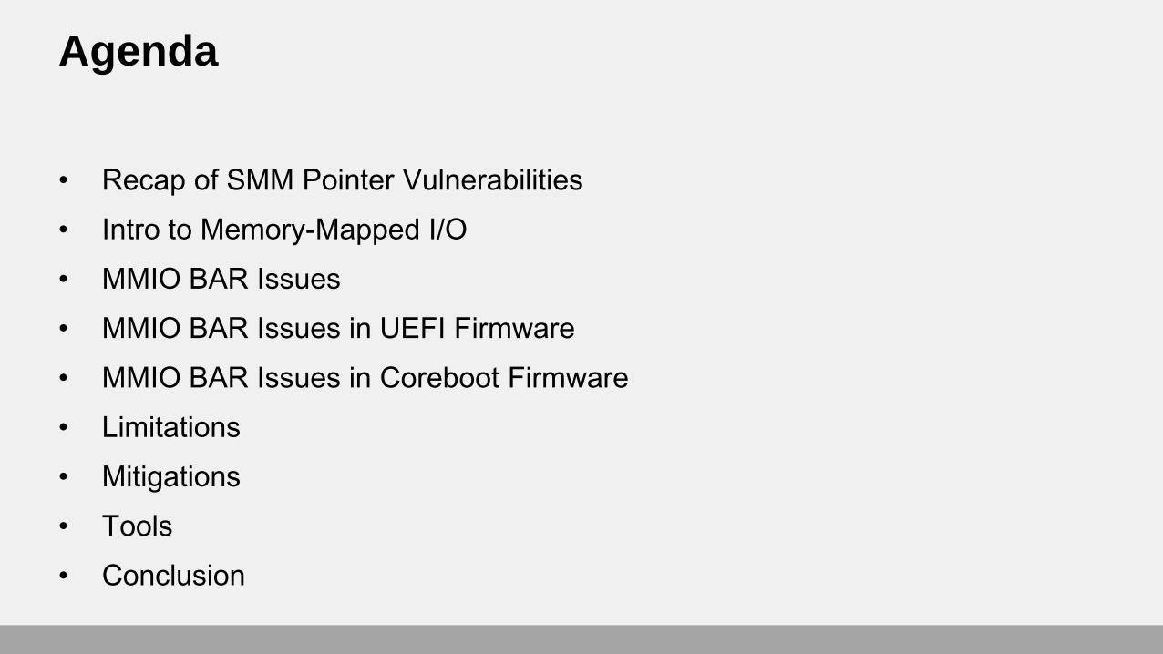
Agenda
• Recap of SMM Pointer Vulnerabilities
• Intro to Memory-Mapped I/O
• MMIO BAR Issues
• MMIO BAR Issues in UEFI Firmware
• MMIO BAR Issues in Coreboot Firmware
• Limitations
• Mitigations
• Tools
• Conclusion

Recap of SMM pointer vulnerabilities

Pointer Arguments to SMI Handlers
Phys Memory
SMI Handlers in SMRAM
OS MemoryRAX (code)
RBX (pointer) SMM communication buffer
Arguments IN, results OUT
SMI
“UEFI” ACPI
Comm Buffer
EDKII
EDKI
Via ACPI table
Directly in registers

Exploiting SMM pointers…
Phys Memory
SMI Handlers in SMRAM
OS MemoryRAX (code)
Fake SMM comm buffer
“UEFI” ACPI
EDKII
EDKI
Via ACPI table
Directly in registers
SMI
Exploit tricks SMI handler to write to an address in SMRAM (Attacking and Defending BIOS in 2015)
Comm Buffer
RBX (pointer)

Attacking hypervisors via SMM pointers…
Phys Memory
SMI Handlers in SMRAM
OS MemoryRAX (code)
Fake SMM comm buffer
VMM protected page
“UEFI” ACPI
EDKII
EDKI
Via ACPI table
Directly in registers
SMI
Comm Buffer
RBX (pointer)
Even though SMI handler check pointers for overlap with SMRAM, exploit can trick it to write to VMM
protected page (Attacking Hypervisors via Firmware and Hardware)

Example: SMIFlash SMI Handler
Reported by ATR to BIOS vendor in June 2014
Similar to publication by Sogeti ESEC Lab

SMI handlers now validate input pointers
SMI handlers now validate pointer + offsets received from the OS for overlap with SMRAM before using it (SmmIsBufferOutsideSmmValid). This does not block exploits using SMI handlers as
proxies to attack hypervisor pages (Hyper-V, Windows 10 Virtual Secure Mode)
Most recently, EDKII implemented CommBuffer at fixed memory location to mitigate attacks on
hypervisors and reporting to Windows through the Windows SMM Mitigations ACPI Table (WSMT)

Memory-Mapped I/O (MMIO)

PCI Express
• PCI Express Fabric consists of PCIe components connected over PCIe
interconnect in a certain topology (e.g. hierarchy)
• Root Complex is a root component in a hierarchical PCIe topology with one or
more PCIe root ports
• Components: Endpoints (I/O Devices), Switches, PCIe-to-PCI/PCI-X Bridges
• All components are interconnect via PCI Express Links
• Physical components can have up to 8 physical or virtual functions
• Some endpoints are integrated into Root Complex

PCIe Config Space Layout
Source: PCI Express Base Specification Revision 3.0

PCI/PCIe Config Space Access
1. Software uses processor I/O ports CF8h (control) and CFCh (data) to access PCI
configuration of bus/dev/fun. Address (written to control port) is calculated as:
bus << 16 | dev << 11 | fun << 8 | offset & ~3
2. Enhanced Configuration Access Mechanism (ECAM) allows accessing PCIe
extended configuration space (4kB) beyond PCI config space (256 bytes)
Implemented as memory-mapped range in physical address space split into
4kB chunks per B:D.F
Register address is a memory address within this range
MMCFG base + bus*32*8*1000h + dev*8*1000h + fun*1000h + offset
100h bytes of
CFG header8 * 100h
per device
32* 8 * 100h
per bus

Memory-Mapped I/O
• Devices need more space for registers
• Memory-mapped I/O (MMIO)
• MMIO range is defined by Base
Address Registers (BAR) in PCI
configuration header
• Access to MMIO ranges forwarded to
devices

MMIO vs DRAM
Low DRAM
SMM Memory
Graphics Memory
Low MMIO
Direct-mapped BIOS,
APIC, TPM…
MMIO
Memory
High DRAM Memory
Top of Low DRAM
4GB
BAR 1 – BAR n
ECAM
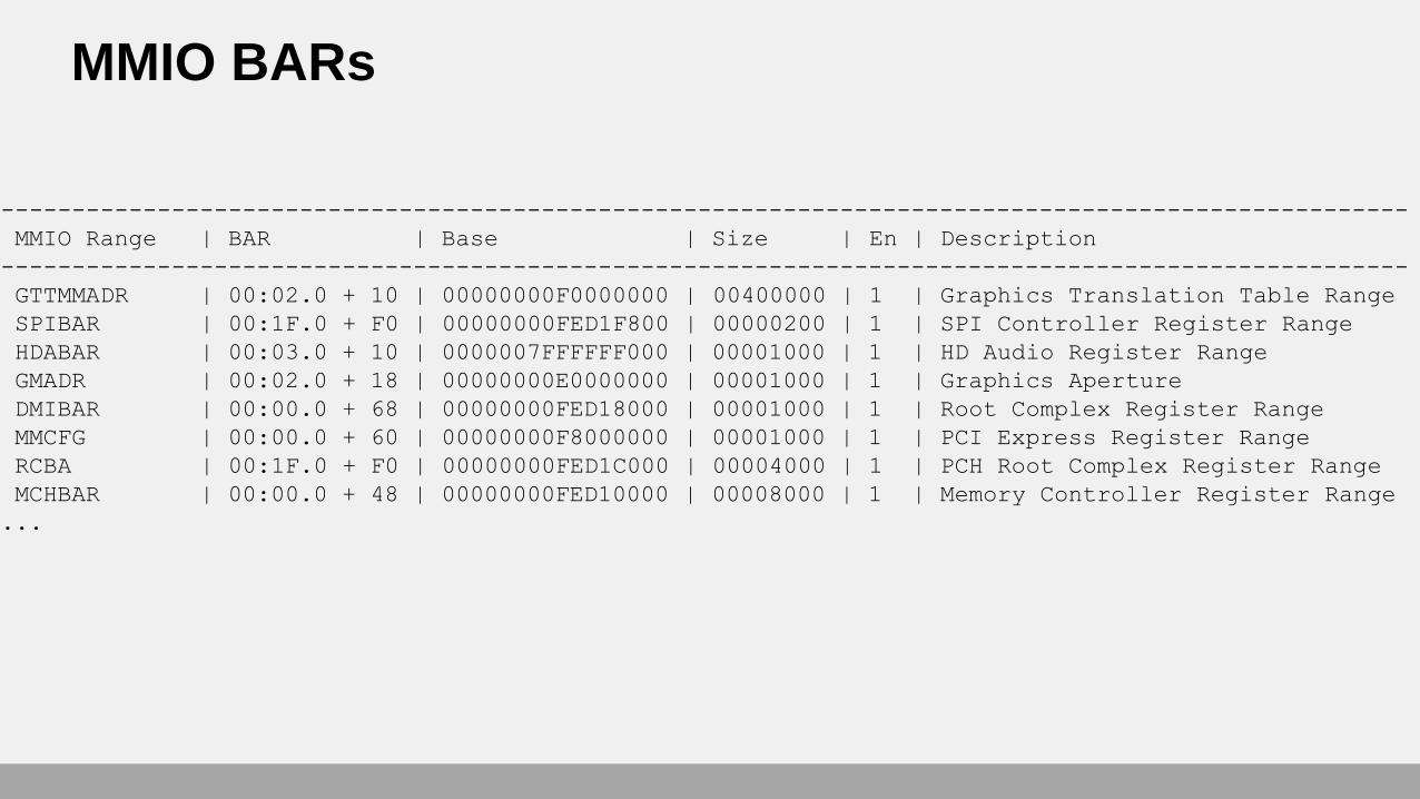
MMIO BARs
---------------------------------------------------------------------------------------------------
MMIO Range | BAR | Base | Size | En | Description
---------------------------------------------------------------------------------------------------
GTTMMADR | 00:02.0 + 10 | 00000000F0000000 | 00400000 | 1 | Graphics Translation Table Range
SPIBAR | 00:1F.0 + F0 | 00000000FED1F800 | 00000200 | 1 | SPI Controller Register Range
HDABAR | 00:03.0 + 10 | 0000007FFFFFF000 | 00001000 | 1 | HD Audio Register Range
GMADR | 00:02.0 + 18 | 00000000E0000000 | 00001000 | 1 | Graphics Aperture
DMIBAR | 00:00.0 + 68 | 00000000FED18000 | 00001000 | 1 | Root Complex Register Range
MMCFG | 00:00.0 + 60 | 00000000F8000000 | 00001000 | 1 | PCI Express Register Range
RCBA | 00:1F.0 + F0 | 00000000FED1C000 | 00004000 | 1 | PCH Root Complex Register Range
MCHBAR | 00:00.0 + 48 | 00000000FED10000 | 00008000 | 1 | Memory Controller Register Range
...

MMIO Range Relocation
• MMIO ranges can be relocated at runtime by the OS
• OS would write new address in BAR registers
• Certain MMIO ranges cannot be relocated at runtime
• Fixed (e.g. direct-access BIOS range)
• Or locked down by the firmware (e.g. MCHBAR)

MMIO BAR Issues

Firmware use of MMIO
Phys Memory
SMI Handlers in SMRAM
OS Memory
Base Address (BAR)
MMIO range
(registers)
Device PCI CFG
Firmware configures chipset and devices
through MMIO
SMI handlers communicate
with devices via MMIO registers

MMIO BAR Issue
Phys Memory
SMI Handlers in SMRAM
OS Memory
Base Address (BAR)
MMIO range
(registers)
Device PCI CFG
SMI
Exploit with PCI access can modify BAR
register and relocate MMIO range
On SMI interrupt, SMI handler firmware
attempts to communicate with device(s)
It may read or write “registers” within
relocated MMIO

Examples of MMIO BARs accessed in SMM
• EHCI (USB 2.0) controller MMIO BAR (B0:D26:F0, B0:D29:F0)
• GBe LAN MMIO BAR (B0:D25:F0)
• Root Complex Block Address (RCBA) on earlier platforms (B0:D31:F0)
• SPI BAR on Skylake or later generations (B0:D31:F5)
• AHCI (SATA) controller MMIO BAR (B0:D31:F2, B0:D31:F5)
• xHCI (USB 3.0) controller MMIO BAR (B0:D20:F0)
• Integrated Graphics Device MMIO BAR (B0:D2:F0)
• B1:D0.F0 MMIO BAR
• …

SPI Controller MMIO BAR (Access to SPI Flash)
# chipsec_util.py uefi var-write B 55555555-4444-3333-2211-000000000000 B.bin
# chipsec_util.py mmio dump SPIBAR
SPI Flash Data
(Variable contents)
SPI Status and Control
SPI Flash Address (address
variable is written to in flash)

Finding MMIO BAR issues at runtime
Goal: Find all MMIO registers modified by SMI handler
1. Dump MMIO range
2. Trigger SMI
3. Dump MMIO range and compare all registers
Problem: many registers are modified by devices all the time! Up to 30,000
registers change in Graphics Device MMIO

Finding MMIO BAR issues at runtime
Goal: Find all MMIO registers modified by SMI handler
1. Dump MMIO range multiple times
2. Find all registers which frequently change without SMM
3. Dump MMIO range
4. Trigger SMI
5. Dump MMIO range and compare all registers
6. Find registers which don’t normally change
7. Repeat this multiple times to confirm suspected registers are actually being modified in SMM
8. Copy original contents of MMIO range to memory
9. Relocate MMIO range (change its base address) to this memory
10. Generate SMI
11. Monitor changes in memory at suspected offsets

Monitoring changes in
USB MMIO BAR

MMIO BAR Issues in UEFI Firmware

Finding MMIO BAR issues in binaries
1. Consider MMIO BAR (MBARA) of GBe LAN device (B0:D25:F0) at offset 0x10
2. Legacy PCIe config address is
(25<<11) + 0x10 = 0xC810
0x8000C810 if with Enable bit (31) set
3. Memory-mapped ECAM address is ECAM base + offset to 4kB page of
B0:D25:F0 + BAR register offset
0xF8000000 + 0xC8010 = 0xF80C8010
4. Look for these constants in the binaries of SMI handlers

GBe LAN MMIO BAR (B0:D25:F0)
Read GBe MMIO BAR register from MMCFG:0xF8000000 + 0x19<<15 + 0x10 =
0xF80C8010
Access to MBARA
MMIO registers

GBe LAN MMIO BAR (B0:D25:F0)
Access to unchecked
MBARA MMIO

EHCI MMIO BAR (B0:D29:F0)Calculate EHCI BAR register address
in MMCFG:0xF8000000 + 0x1D<<15 + 0x10
Read EHCI MMIO BAR
Modify MMIO register 0x20 in EHCI MMIO
range

Finding MMIO BAR issues in binaries
Identify functions reading PCI config registers via legacy or ECAM access and
find ones reading BAR registers using above constants
Access to register 0x88 in B0:D31:F0Legacy PCI config read
Extended PCIe config access through MMCFG

MMIO BAR Issues in Coreboot Firmware

Finding MMIO BAR issues in the source code
1. Find functions within SMI handlers which read MMIO BAR PCI config registers
(offsets 0x10-0x24 or chipset specific offsets for integrated devices)
BAR registers can be read using memory-mapped config reads (offsets in ECAM memory
space). In this case, normal memory reads will be used
2. Find all memory accesses to offsets off of BAR addresses within SMI handlers
3. Can often search the names of the BAR registers and MMIO ranges (e.g.
SPI_BAR0, RCBA/RCRB, PCI_BASE_ADDRESS etc.)

mainboard_io_trap_handler SMI handlerbar pointer points to
MMIO range of device
B1:D0.F0 which can be
modified by an attacker
SMI handler then uses bar
pointer to write to LVTMA_BL_MOD_LEVEL
offset (when adjusting
brightness level)
SMI handler can be invoked by
properly configuring I/O Trap
hardware with BRIGHTNESS_UP/DOWN function

southbridge_smi_sleep SMI handler
reg_base pointer points
relocateable IGD MMIO
SMI handler then uses reg_base to read-modify-
write PP_CONTROL register
Vulnerable backlight_off is
invoked when system goes to S5

Limitations
1. Exploit can overwrite specific offsets off of aligned addresses
• MMIO ranges are typically normally (size) aligned
• Most MMIO ranges are 4kB large (Graphics MMIO is 2-4MB)
• Example: 16kB aligned Root Complex Base + 0x38xx (SPI registers)
• PCI architecture allows MMIO ranges as small as 16 bytes
2. Exploit may not be able to control values written
• Firmware SMI handlers typically write specific values to MMIO registers
• Often do Read-Modify-Write: reg +/- 0x10
• Certain SMI handler may write attacker-supplied data
• SetVariable SMI handler write contents of UEFI variable supplied by the OS to
SPI_DATAx registers in SPIBAR MMIO range

Limitations
1. Many conditions for SMI handler to start communicating with I/O device/controller Device present/enabled, mode/feature supported
Is platform in ACPI mode?
Other SMM code may also use fake MMIO (and hang)
SMI may get triggered on difficult events – power button, on S3 resume, etc.
2. Often, SMI handlers implement protocol rather than just reading or writing to MMIO registers IF Bit X in Reg1 is set THEN Write to Reg2
Poll until certain bits are set/cleared in MMIO register (wait until SPI cycle complete)
When SMI handler waits for the device to respond or cycle to complete then it’ll hang after MMIO BAR is relocated
3. Non PCI-architectural BAR registers are locked down by boot firmware and cannot be relocated (MCHBAR, DMIBAR etc.)

Mitigations
Option 1. SMI handlers can verify MMIO BAR doesn’t overlap with SMRAM
Option 2. Firmware can verify that MMIO BAR is not in DRAM (e.g. between
TOLUD and 4GB or above TOUUD). This would ensure all BARs used by
firmware are within MMIO
Option 3. Firmware can reserve default MMIO range for all BARs. Before
accessing MMIO range, SMI handlers can relocate BARs to the default range if
they point to somewhere else

SPIBAR Mitigation Example
• On latest platforms, SPI MMIO is a separate 4kB range rather than a part of
Root Complex MMIO
• Firmware reserves 0xFE010000 page for SPI MMIO and programs
SPI_BAR0 register in SPI controller with this address.
• On any PCH SMI, SMI handler checks SPI_BAR0 and restores it to 0xFE010000 if it’s been relocated.
Relocating SPI BAR
to memoryvar-write triggers SMI
writing variable to SPI
BAR. It succeeded!
SMI handler restored SPI
BAR to the original location

Tools to assist in finding/analyzing these issues
tools.smm.rogue_mmio_bar
Attempts to create fake MMIO ranges in memory, relocate hardware MMIO
BARs to the fake memory, then observe changes made by SMI handlers in
relocated MMIO ranges
tools.smm.bar
Simply monitors changes made by SMI handlers in MMIO registers of specified
MMIO BARs
Conclusion
• The root cause is that firmware assumes hardware is trusted
• Hardware registers like PCI Base Address Registers can be
modified by runtime software (some are locked down)
• Firmware shouldn’t assume addresses in BAR registers are
correct and should treat them as untrusted input
• Boot firmware should also validate contents of BAR registers upon
resume from sleep if it restores them from S3 boot script

Thank You!