bandpass analog-to-digital conversion for …cis.stanford.edu/icl/wooley-grp/alois/icl1_1.pdf ·...
TRANSCRIPT
BANDPASS ANALOG-T O-DIGIT AL CONVERSION
FOR WIRELESS APPLICATIONS
by
Adrian Karl Ong
September 1998
Prepared under
Semiconductor Research Corportation
Contract No. 95-DJ-703
Integrated Circuits Laboratory
Stanford Electronics Laboratories
Stanford University, Stanford, California

ii
Copyright © 1999
by
Adrian K. Ong
All Rights Reserved
iii
Abstract
Oversampled bandpass A/D converters based on sigma-delta (Σ∆) modulation can be used
to robustly digitize the narrowband intermediate frequency (IF) signals that arise in radios
and cellular systems. Digitization of the IF processing confers several important advan-
tages in a receiver, including greater reliability, potentially lower power dissipation, and
improved performance as technology scales. Moreover, by converting to digital at the IF
location, the problems of low frequency (1/f ) noise and dc offset are avoided.
The implementation of a high-speed bandpassΣ∆ modulator that achieves the large
dynamic range needed for narrowband wireless-channel digitization involves significant
challenges that are explored in this research. This dissertation describes a new two-path
architecture for a fourth-order, bandpassΣ∆ modulator that is more tolerant of analog cir-
cuit limitations at high sampling speeds than conventional implementations based on the
use of switched-capacitor biquadratic filters. Nonideal effects relating to this new two-path
architecture, such as timing jitter, path mismatch, and potential instability are described
and analyzed. An experimental prototype employing the two-path topology has been inte-
grated in a 0.6-µm, single-poly, triple-metal CMOS technology with capacitors
synthesized from a stacked-metal structure. Two interleaved paths clocked at 40 MHz dig-
itize a 200-kHz bandwidth signal centered at 20 MHz with 75 dB of dynamic range while

iv
suppressing the undesired mirror image signal by 42 dB. At low input signal levels, the
mixing of spurious tones at dc andfs/2 with the input appears to degrade the performance
of the modulator; out-of-band sinusoidal dither is shown to be an effective means of avoid-
ing this degradation. The experimental modulator dissipates 72 mW from a 3.3-V supply.
An analysis of noise in the experimental prototype reveals that its inband noise floor is
dominated by a combination of amplifier noise and thermal noise from switches. The mea-
sured dynamic range of the experimental prototype lies within 2 dB of that predicted by
hand analysis.

v
Acknowledgments
I wish to acknowledge the many people who have assisted me in this work and made my
experience at Stanford so enjoyable. First and foremost, I thank Professor Bruce Wooley
for having accepted me into his research group when I was capable of little, except to
articulate my desire to do research in electronic circuit design. He has given me excellent
guidance throughout the years and has instilled in me an appreciation for communicating
clearly. He impresses me as someone who combines an uncommon ear for language with
the rare ability to elicit clarity from the writing of students through his bold editing. Any
obfuscation in this thesis is reflective solely of my own inadequacy. In the future, I will
strive to apply the same exacting standards to myself as Professor Wooley has to me.
My orals committee, Professor Edward McCluskey, Professor Donald Cox, and Pro-
fessor Krishna Saraswat deserve sincere thanks for their time and efforts. I also thank
Professors McCluskey and Cox for serving on my dissertation reading committee.
Throughout this work, Professor Tom Lee deserves special recognition for often
reviewing my ideas and offering good suggestions. His excellent sense of humor and love
of story telling enhanced my interactions with him.
In addition, I gratefully appreciate the guidance and feedback provided by Bill McFar-
land and the members of his research staff at HP Labs. In particular, Dr. David Su and
vi
Dr. Ken Nishimura have been extremely helpful. The Center for Integrated Systems,
through the Faculty-Mentor-Associate fellowship, was instrumental in establishing the
relationship I developed with Hewlett-Packard.
I would be remiss if I failed to mention Ann Guerra who has been very helpful with
many matters. She exemplifies the highest standards of orderly and swift execution. Also,
without her excellent disposition and keen sense of humor, the working environment here
wouldn’t be nearly as pleasant as everyone in CIS can attest to.
The computer support provided by Joe Little and Charlie Orgish has been extremely
valuable and is deeply appreciated.
My work has benefited tremendously from my interaction with past and present mem-
bers of the Wooley research group, as well as numerous students from the Lee, Horowitz,
and Wong research groups. In particular, among my colleagues, I am very thankful for the
assistance of Dr. David Shen, Dr. Sha Rabii, Dr. Stefanos Sidiropolous, and Joe Ingino in
all matters. Joe deserves special recognition. We joined Professor Wooley’s group at about
the same time in 1993 and even, for awhile, shared an office where we typed together.
Throughout the years, Joe has been a good friend and excellent provider of technical
advice and many opinions. I have also been gifted with the stalwart friendship and assis-
tance of many other people including Dr. Patrick Yue, Dr. Fred Sugihwo, Alvin Loke,
Arvin Shahani, Derek Shaeffer, S. S. Mohan, Ali Hajimiri, Mar Hershenson, Katayoun
Falakshahi, Dr. Tallis Blalack, Jim Burnham, Dwight Thompson, Ali Tabatabaei, Sotirios
Limotyrakis, Min Xu, James Pan, Ken Yang, Birdy Amrutur, and Gu-Yeon Wei. Prior to
their graduation, I also had the pleasure of interacting with Dr. Marc Loinaz,
Dr. Chye-Huat Aw, Dr. Mehrdad Heshami, Dr. Masoud Zargari, and Dr. Peter Capofreddi.
In 1994, I was privileged to participate in the NSF Summer Institute in Japan, during
which I interned at the Toshiba Research and Development Center in Kawasaki, Japan. I
thank Dr. Fujio Masuoka for accepting me into his laboratory and Dr. Koji Sakui for act-
ing as my host there. Also, I am glad to have met Susumu Shuto, Yoko Shuto, and Toru
Tanzawa who befriended me during my stay. During the same summer, Prof. Young-June
vii
Park of Seoul National University made it possible for me to visit his laboratory and enjoy
Seoul as well.
Outside of Stanford, many people have given their unflagging support and friendship
to me throughout my years here. I was fortunate to have met David Lin several years ago,
at the Mountain View Small Brewers’ Festival no less. Since then, David and Pearl Lin
have always encouraged and befriended me. I am particularly inspired by David’s infec-
tious enthusiasm for technical studies, which dates back to when he was a student of
Ginzton and Terman. At the risk of omitting someone, I thank the following people for
stimulation and refreshment when most needed: Vicki Jew, Michael Ching, Dr. Thomas
Tsao, Janice Tsao, Charles Cohen, Dr. Martha Arroyo, Ive Aaslid, Michael Pascual, Liza
Riguerra, Rina Hui, Bruno Garlepp, Bruce Chu, Janice Chen, Ray Chiang, Julie Ngau,
Pauline Jew, Isabel Koh, Insik Rhee, Prof. Jake Baker, Srenik Mehta, Mani Varadarajan,
Robert Hsieh, Wen Hsieh, Sue-won So, Rosenna Yau, Dr. Mark Ford, Guido Appenzeller,
Gary Brown, Ann Matsubara, Dr. Stanley Pau, and Dr. Anthony Chou.
I gratefully acknowledge the Hewlett-Packard Corporation and the Semiconductor
Research Corporation for funding various aspects of this work.
Finally, I thank my family, Kwok, Diana, Julian, and Jacqueline, for always encourag-
ing my studies, and my earlier professors at the University of California, Berkeley for
having laid the foundation that prepared me for graduate school. I am especially grateful
to Professor Donald O. Pederson for always having had the time and patience to teach and
advise me when I was an undergraduate.

viii
ix
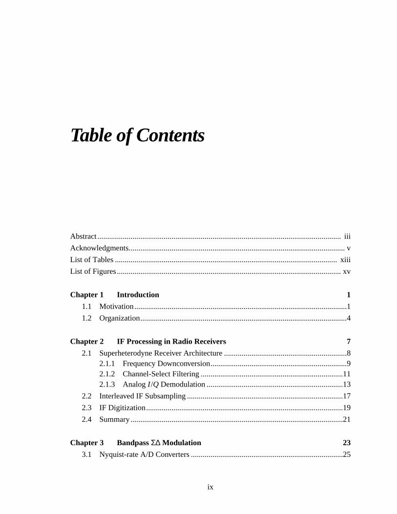
Table of Contents
Abstract............................................................................................................................. iii
Acknowledgments............................................................................................................... v
List of Tables.................................................................................................................. xiii
List of Figures................................................................................................................... xv
Chapter 1 Intr oduction 1
1.1 Motivation.............................................................................................................1
1.2 Organization..........................................................................................................4
Chapter 2 IF Processing in Radio Receivers 7
2.1 Superheterodyne Receiver Architecture...............................................................82.1.1 Frequency Downconversion......................................................................92.1.2 Channel-Select Filtering.........................................................................112.1.3 AnalogI /Q Demodulation......................................................................13
2.2 Interleaved IF Subsampling................................................................................17
2.3 IF Digitization.....................................................................................................19
2.4 Summary.............................................................................................................21
Chapter 3 BandpassΣ∆ Modulation 23
3.1 Nyquist-rate A/D Converters..............................................................................25
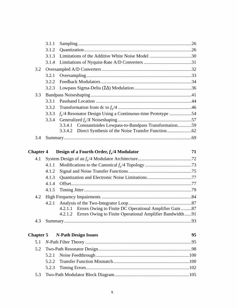
x
3.1.1 Sampling.................................................................................................263.1.2 Quantization............................................................................................263.1.3 Limitations of the Additive White Noise Model....................................303.1.4 Limitations of Nyquist-Rate A/D Converters.........................................31
3.2 Oversampled A/D Converters.............................................................................323.2.1 Oversampling..........................................................................................333.2.2 Feedback Modulators..............................................................................343.2.3 Lowpass Sigma-Delta (Σ∆) Modulation.................................................36
3.3 Bandpass Noiseshaping......................................................................................413.3.1 Passband Location..................................................................................443.3.2 Transformation from dc tofs/4 ...............................................................463.3.3 fs/4 Resonator Design Using a Continuous-time Prototype...................543.3.4 Generalizedfs/X Noiseshaping...............................................................57
3.3.4.1 Constantinides Lowpass-to-Bandpass Transformation............593.3.4.2 Direct Synthesis of the Noise Transfer Function.....................62
3.4 Summary.............................................................................................................69
Chapter 4 Design of a Fourth-Order , fs/4 Modulator 71
4.1 System Design of anfs/4 Modulator Architecture..............................................724.1.1 Modifications to the Canonicalfs/4 Topology........................................734.1.2 Signal and Noise Transfer Functions......................................................754.1.3 Quantization and Electronic Noise Limitations......................................774.1.4 Offset.......................................................................................................774.1.5 Timing Jitter............................................................................................79
4.2 High Frequency Impairments.............................................................................844.2.1 Analysis of the Two-Integrator Loop......................................................87
4.2.1.1 Errors Owing to Finite DC Operational Amplifier Gain.........874.2.1.2 Errors Owing to Finite Operational Amplifier Bandwidth......91
4.3 Summary.............................................................................................................93
Chapter 5 N-Path Design Issues 95
5.1 N-Path Filter Theory...........................................................................................95
5.2 Two-Path Resonator Design................................................................................985.2.1 Noise Feedthrough................................................................................1005.2.2 Transfer Function Mismatch.................................................................1005.2.3 Timing Errors........................................................................................102
5.3 Two-Path Modulator Block Diagram................................................................105
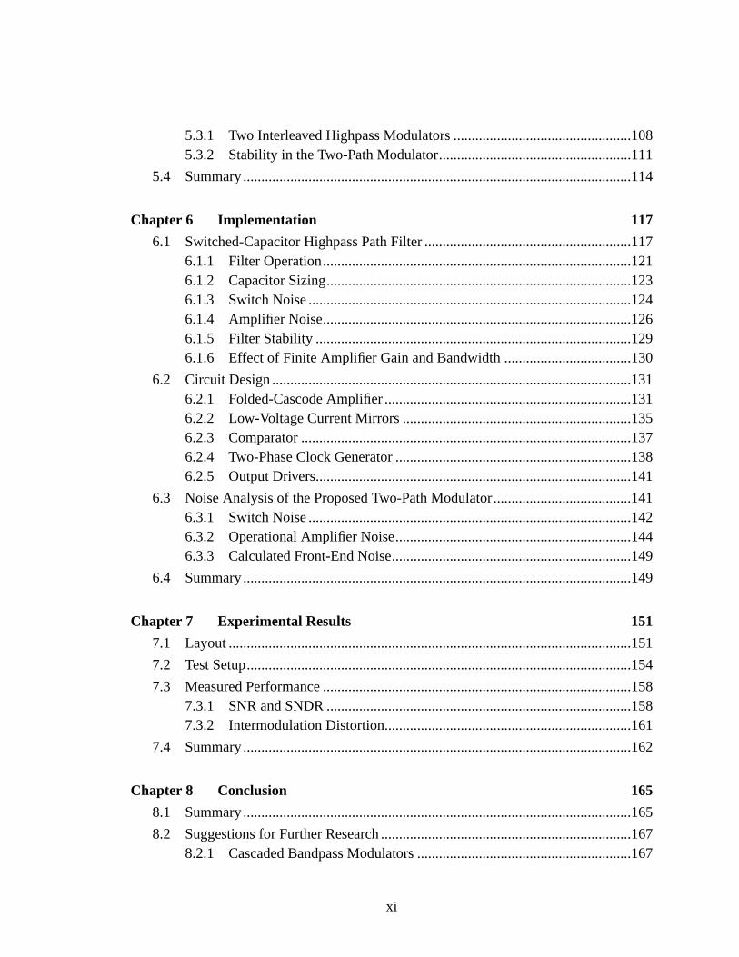
xi
5.3.1 Two Interleaved Highpass Modulators.................................................1085.3.2 Stability in the Two-Path Modulator.....................................................111
5.4 Summary...........................................................................................................114
Chapter 6 Implementation 117
6.1 Switched-Capacitor Highpass Path Filter.........................................................1176.1.1 Filter Operation.....................................................................................1216.1.2 Capacitor Sizing....................................................................................1236.1.3 Switch Noise.........................................................................................1246.1.4 Amplifier Noise.....................................................................................1266.1.5 Filter Stability.......................................................................................1296.1.6 Effect of Finite Amplifier Gain and Bandwidth...................................130
6.2 Circuit Design...................................................................................................1316.2.1 Folded-Cascode Amplifier....................................................................1316.2.2 Low-Voltage Current Mirrors...............................................................1356.2.3 Comparator...........................................................................................1376.2.4 Two-Phase Clock Generator.................................................................1386.2.5 Output Drivers.......................................................................................141
6.3 Noise Analysis of the Proposed Two-Path Modulator......................................1416.3.1 Switch Noise.........................................................................................1426.3.2 Operational Amplifier Noise.................................................................1446.3.3 Calculated Front-End Noise..................................................................149
6.4 Summary...........................................................................................................149
Chapter 7 Experimental Results 151
7.1 Layout...............................................................................................................151
7.2 Test Setup..........................................................................................................154
7.3 Measured Performance.....................................................................................1587.3.1 SNR and SNDR....................................................................................1587.3.2 Intermodulation Distortion....................................................................161
7.4 Summary...........................................................................................................162
Chapter 8 Conclusion 165
8.1 Summary...........................................................................................................165
8.2 Suggestions for Further Research.....................................................................1678.2.1 Cascaded Bandpass Modulators...........................................................167
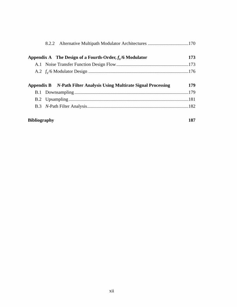
xii
8.2.2 Alternative Multipath Modulator Architectures...................................170
Appendix A The Design of a Fourth-Order , fs/6 Modulator 173
A.1 Noise Transfer Function Design Flow..............................................................173
A.2 fs/6 Modulator Design......................................................................................176
Appendix B N-Path Filter Analysis Using Multirate Signal Processing 179
B.1 Downsampling..................................................................................................179
B.2 Upsampling.......................................................................................................181
B.3 N-Path Filter Analysis.......................................................................................182
Bibliography 187

xiii
List of Tables
Table 1.1: Top ten cellular markets in terms of (a) subscribers, and(b) penetration per 100 population in 1997........................................... 2
Table 6.1: Simulated transconductances of the primary noise-contributingtransistors in the folded-cascode amplifier shown in Figure6.7...... 135
Table 7.1: Performance summary of the prototype, two-path modulator.......... 164

xiv
xv
List of Figures
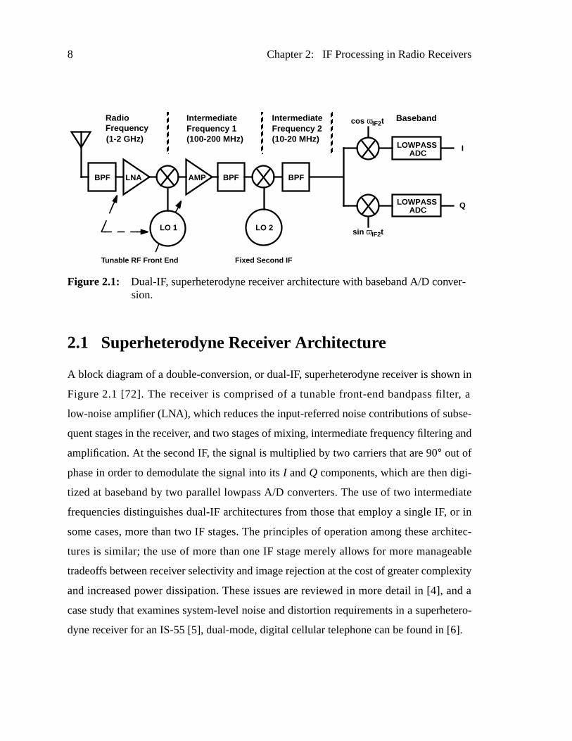
Figure2.1: Dual-IF, superheterodyne receiver architecture with basebandA/D conversion......................................................................................8
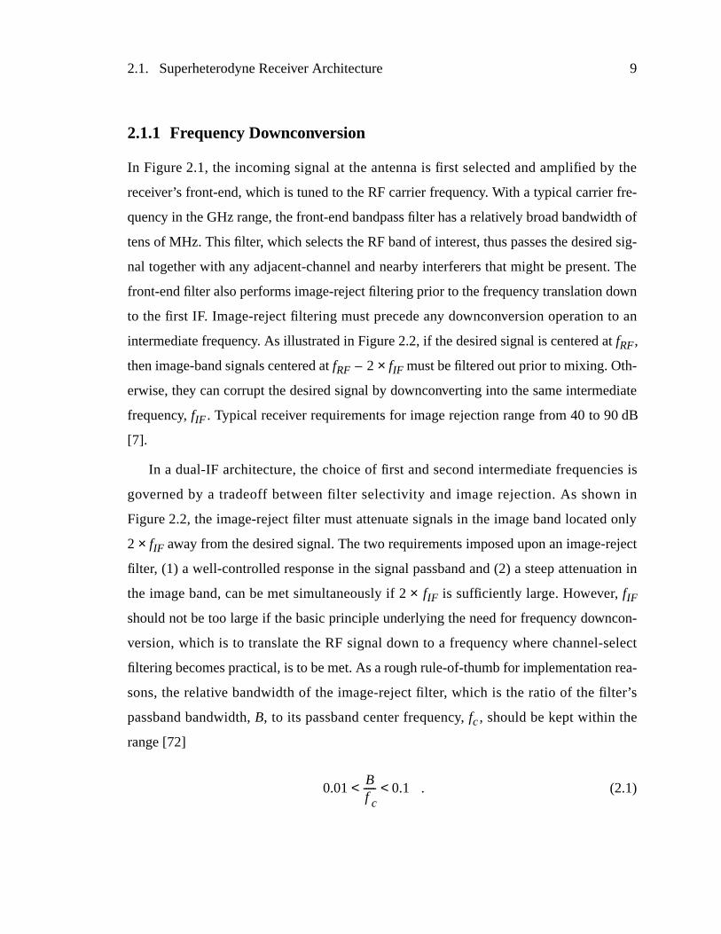
Figure2.2: (a) The spectrum ofxRF(t), prior to filtering and mixing, whichshows an undesired signal in the image band, and (b) the spectrumof the intermediate frequency signal,xIF (t), following filteringand mixing...........................................................................................10
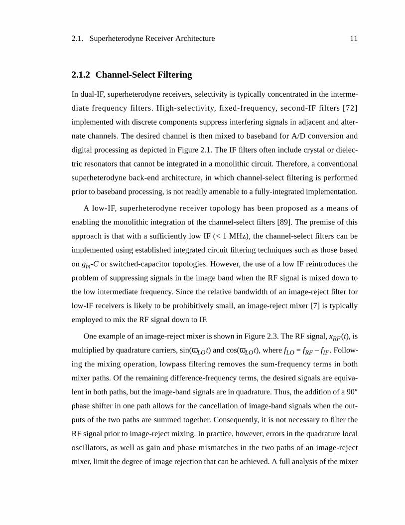
Figure2.3: Hartley image-reject mixer...................................................................12
Figure2.4: AnalogI/Q demodulation with a phase error, φ, in the quadraturelocal oscillators....................................................................................14
Figure2.5: Frequency spectrum ofxb(t) after analogI/Q demodulation witha phase error, φ, between carriers nominally in quadrature.................15
Figure2.6: Superheterodyne receiver with an interleaved samplingI/Qdemodulator..........................................................................................18
Figure2.7: Superheterodyne receiver incorporating IF digitization viabandpass A/D conversion.....................................................................19
Figure2.8: Digital I /Q demodulation of a signal centered atfs/4..........................20
Figure3.1: Fundamental operations comprising analog-to-digitalconversion............................................................................................25
Figure3.2: An analog signal that has been (a) sampled at the Nyquist rate,and (b) oversampled.............................................................................27
Figure3.3: (a) Transfer characteristic and (b) error characteristic of auniform quantizer.................................................................................28
xvi
Figure3.4: Probability density function of additive, white quantizationnoise.....................................................................................................29
Figure3.5: Linearized, stochastic model of quantizer............................................29
Figure3.6: Power spectral density of quantization noise when the inputsignal is oversampled...........................................................................33
Figure3.7: Feedback modulator.............................................................................34
Figure3.8: First-order lowpassΣ∆ modulator........................................................37
Figure3.9: Second order lowpassΣ∆ modulator. ..................................................38
Figure3.10: First-, second-, and third-order lowpass noise transfer functions........39
Figure3.11: Lth-order lowpassΣ∆ modulator..........................................................40
Figure3.12: Synthesizing a complex-valued transfer function from real-valued building blocks.........................................................................43
Figure3.13: Antialiasing filtering in a bandpass modulator.....................................45
Figure3.14: Canonical, fourth-order, fs/4 Σ∆ modulator. ........................................47
Figure3.15: Zeros of the noise transfer function of a fourth-order,fs/4 modulator. .....................................................................................48
Figure3.16: Undecimated spectrum of a canonical, fourth-order,fs/4 modulator. .....................................................................................52
Figure3.17: SNR vs. Input Signal Level of a canonical, fourth-order,fs/4 modulator. .....................................................................................52
Figure3.18: (a) Undecimated spectrum of a canonical, fourth-order,fs/4 modulator. A close-in view around (b) dc and(c) fs/2 (40 MHz).................................................................................53
Figure3.20: Fourth-order, fs/4 modulator implemented with resonatorsdesigned using the bilinear transform..................................................56
Figure3.19: Magnitude and phase responses of a second-order, fs/4 resonatorwith the transfer function, (a)H1(z), (3.24), and (b)H2(z), (3.39)......57
Figure3.21: (a) Undecimated spectrum of anfs/4 modulator with resonatorsderived from the bilinear transform. A close-in view around(b) dc and (c)fs/2.................................................................................58
Figure3.22: A possiblez-domain implementation of a generalizedωo resonatorwith the transfer function (3.45)..........................................................62
Figure3.23: Fourth-order, fs/6 modulator implemented with resonatorsdesigned using the Constantinides transform......................................62
Figure3.24: Undecimated output spectrum of anfs/6 modulator withresonators derived from Constantinides transform. A close-inview around (b) dc and (c)fs/2. ...........................................................63
xvii
Figure3.25: Implementation of the forward path filter, A(z), using a cascadeof resonators.........................................................................................68
Figure4.1: Proposedfs/4 modulator topology with internal signal scalingand delays in the forward path of both resonators...............................74
Figure4.2: Simulated inband signal-to- noise ratio vs. the gain of thefirst resonator........................................................................................75
Figure4.3: Comparison of signal swings at the outputs of the (a) first and(b) second resonators for the canonicalfs/4 modulator vs. theproposedfs/4 modulator for an –10 dB input signal............................76
Figure4.4: Output spectrum with a close-up view around dc when thecomparator offset is (a) zero, and (b)∆/40, where∆ = 1 V. ................78
Figure4.5: A discrete model of the sampling process when the samplingtimes,nT, are perturbed by a random process,ζ(t)..............................80
Figure4.6: Degradation of the inband signal-to-noise ratio due to a samplingclock derived from an oscillator with high phase noise sidebands......83
Figure4.7: Behavioral simulation showing the broad increase in the noisefloor that occurs as the standard deviation of the jitter increases.........84
Figure4.8: Idealfs/4 resonator magnitude response..............................................85
Figure4.9: (a) Block and (b) circuit diagram of anfs/4 resonatorimplemented using a two-integrator loop............................................86
Figure4.10: Switched-capacitor integrator with the output delayed byone-half sample period.........................................................................87
Figure4.11: Pole locations of thefs/4 resonator transfer function under theinfluence of finite dc operational amplifier gain..................................89
Figure5.1: GeneralizedN-path filter structure.......................................................96
Figure5.2: Nyquist-band frequency response of (a) an individual path,and (b) anN-path filter. ........................................................................97
Figure5.3: (a) Two-path implementation of anfs/4 resonator, and (b) thefrequency response of the path filter compared with that of theresonator...............................................................................................99
Figure5.4: Mirror image of the signal introduced by gain and phasemismatches into the output spectrum of the modulator. ....................102
Figure5.5: An example of a systematic timing error, ∆e, that results whensampling a continuous-time signal,xc(t), with skewedtwo-phase clocks................................................................................103
Figure5.6: Output spectrum of a sampled sinusoid with frequency fx andunity amplitude when the sampling time is perturbed for everyother sample by∆e. Spectrum is symmetric around dc.....................105
xviii
Figure5.7: (a) Output spectrum of the proposed two-path modulator witha systematic timing error, ∆e, of 100 ps, and (b) a zoomed-inview of the passband centered aroundfs/4. .......................................106
Figure5.8: Fourth-order bandpass modulator implemented using two-pathresonators...........................................................................................107
Figure5.9: Partitioning of bandpass modulator into two independenthighpass paths....................................................................................109
Figure5.10: Output spectrum with a close-up view around dc when (a) bothcomparators do not have an offset, and (b) one comparator has anoffset of∆/40 and the other has an offset of –∆/40;∆ = 1 V.............110
Figure5.11: Inband image that is introduced by comparator mismatch inthe two-path modulator for input signal frequencies,(a) fx = 20.053MHz, and (b)fx = 20.133MHz..................................112
Figure5.12: One path of the proposed modulator with capacitor mismatcherrors in the path filters reflected in the feedback factor, K. Theinternal states of the path are denotedA andB. .................................113
Figure5.13: The internal states,A andB, of one modulator path that is subjectedto a recovery test.A andB are preloaded to 5× |Vref| and thefeedback factor, K, is equal to (a) 1.01 and (b) 1.02. The inputsignal amplitude is –3 dB relative toVref /2.......................................115
Figure6.1: Fully-differential, switched-capacitor implementation of thehighpass path filter with capacitor values for the first- and second-stage filters.........................................................................................118
Figure6.2: Switch networks used to sample the (a) input signal and(b) output of the amplifier in the highpass path filter. Transistorsizes are inµm...................................................................................120
Figure6.3: Switched-capacitor highpass path filter configured duringthe (a) sampling phase,ΦS, and (b) charge-redistributionphase, ΦT............................................................................................122
Figure6.4: Metal sandwich capacitor implementation........................................123
Figure6.5: (a) MOS sample-and-hold, and (b) its equivalent noisy circuitwhenΦS is high.................................................................................125
Figure6.6: Single-ended representation of the proposed highpass pathfilter with an input,VIN, and an input-referred amplifier noisesource,eamp........................................................................................127
Figure6.7: Folded-cascode operational amplifier. ...............................................132
Figure6.8: Simulated frequency response of the folded-cascode operationalamplifier with a 2 pF load capacitance on each output......................133
Figure6.9: Switched-capacitor common-mode feedback....................................134
xix
Figure6.10: Low-voltage current mirror biasing...................................................136
Figure6.11: Dynamic latch used as the comparator core......................................138
Figure6.12: Two-phase clock generator.................................................................139
Figure6.13: Differential logic gates, (a) NOR and (b) inverter. ............................140
Figure6.14: Current-mode output driver................................................................142
Figure6.15: (a) Block diagram and (b) single-ended switched-capacitorrealization of a single path of the proposed two-path modulatorwith amplifier noise modeled by two independent sources,eamp1 andeamp2. .................................................................................145
Figure7.1: Die photo of the prototype two-path modulator.................................152
Figure7.2: An example layout of matched 300 fF, 750 fF, and 1.5 pFcapacitors using a 150fF unit cell and dummy strips liningthe periphery of the array. ..................................................................154
Figure7.3: Experimental test setup......................................................................155
Figure7.4: Spectrum of undecimated bitstream...................................................157
Figure7.5: Spectrum of complex baseband signal...............................................157
Figure7.6: Measured SNR and SNDR.................................................................158
Figure7.7: Tones in the undecimated spectrum...................................................159
Figure7.8: Application of out-of-band sinusoidal dither. ....................................160
Figure7.9: Measured SNR and SNDR when dither has been applied to theexperimental modulator. ....................................................................161
Figure7.10: Intermodulation spurs arising from third-order nonlinearitiesin the modulator. ................................................................................162
Figure7.11: Measured two-tone test results for (a) two high phase noisesignal sources, and (b) one low phase noise source and one highphase noise source..............................................................................163
Figure8.1: Block diagram of a three-path,fs/6 modulator. .................................171
Figure8.2: Undecimated spectrum of a three-path,fs/6 modulator. ....................172
FigureA.1: Magnitude response of the fourth-order,fs/6 noise transferfunction, (A.3), designed iteratively using MATLAB......................175
FigureA.2: Magnitude response of a fourth-order,fs/6 modulator with aButterworth noise transfer function designed iteratively usingMATLAB. .........................................................................................176
FigureA.3: SNR vs. Input Signal Level of a fourth-order,fs/6 modulatorwith a Butterworth noise transfer function.......................................177
FigureB.1: Block diagram of anM-fold downsampler with an example ofdownsampling by a factor of two on an input signal,x[n]. ...............180
xx
FigureB.2: Spectrum of (a)x[n] and (b)xd[n] with the input samplingrate, 1/T, normalized to unity............................................................181
FigureB.3: Block diagram of anL-fold upsampler with an example ofupsampling by a factor of two on an input signal,x[n]. ...................182
FigureB.4: Frequency spectrum of (a)x[n] and (b)xe[n]. ..................................183
FigureB.5: An N-path filter represented as (a) interleaved path filters, and(b) a multirate, discrete-time system that can be analyzed inthez-domain......................................................................................184
1
Chapter
1 Introduction
The role and infrastructure of wireless communications have grown dramatically since the
initial deployment of the cellular mobile telephone system in the 1980s. From its modest
beginnings characterized by a low subscriber base with telephones having radio transceiv-
ers only slightly more sophisticated than two-way FM radios, global cellular radio systems
now encompass over 150 million subscribers and enable new paradigms of access includ-
ing paging, facsimile, and data services, in addition to voice. The impressive rate of
growth in both subscriber base and technological innovation will remain unchecked as
latent markets in the Asia/Pacific region and the Indian subcontinent emerge. It has been
predicted that there will be 350 million users of mobile communications worldwide by
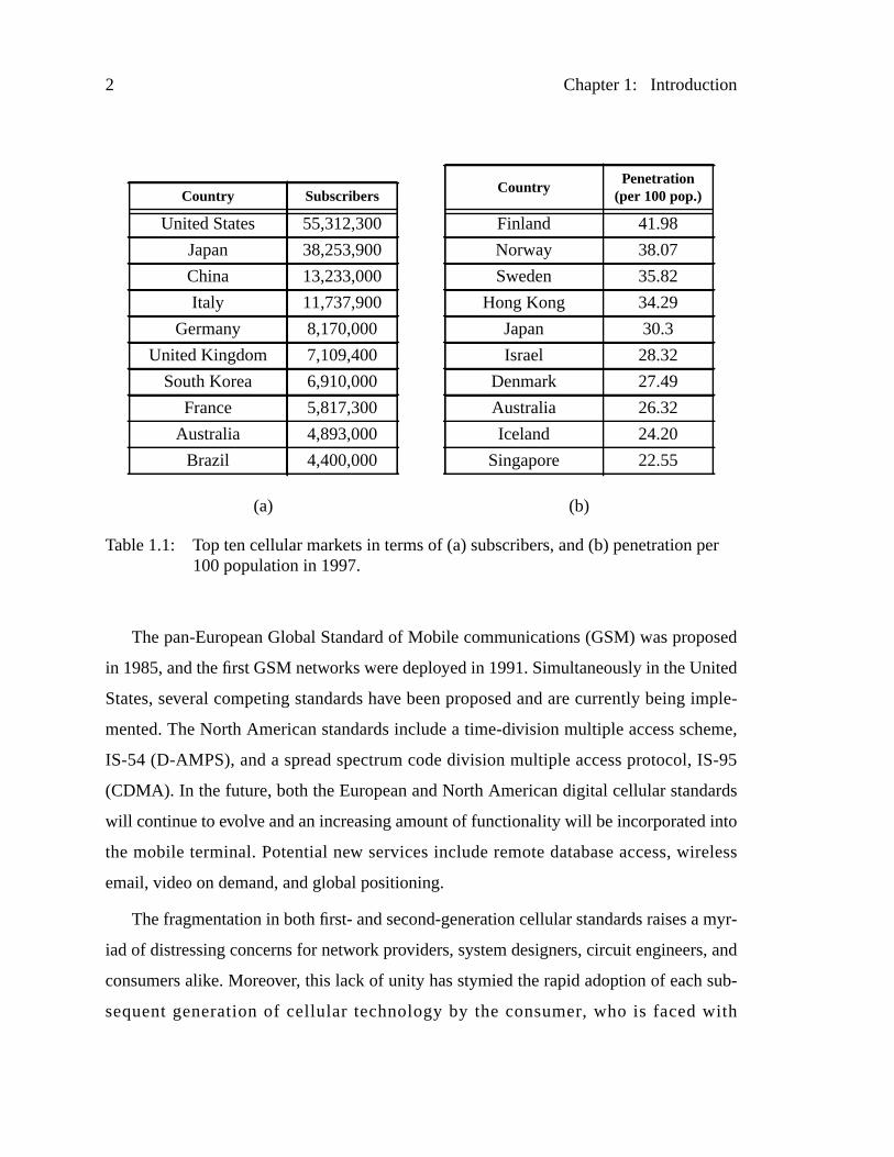
2005. Tables1.1(a) and (b) summarize the top ten cellular markets in terms of subscribers
and penetration in 1997 [1].
1.1 Moti vation
First-generation analog cellular systems such as Advanced Mobile Phone System (AMPS)
in the United States, Nordic Mobile Telephone (NMT) in the Scandinavian countries, and
Total Access Communication System (TACS) in the United Kingdom were only intended
for speech communication. Therefore, the early standards could not accommodate mobile
users who demanded value-added services such as paging and short messaging functions.
In addition, the early standards were marked by their incompatibility, thus restricting
mobile users to the area served by their network provider. These limitations stimulated the
development of second-generation, unified, cellular standards that embraced a robust
data-carrying capacity as well.
2 Chapter 1: Introduction
The pan-European Global Standard of Mobile communications (GSM) was proposed
in 1985, and the first GSM networks were deployed in 1991. Simultaneously in the United
States, several competing standards have been proposed and are currently being imple-
mented. The North American standards include a time-division multiple access scheme,
IS-54 (D-AMPS), and a spread spectrum code division multiple access protocol, IS-95
(CDMA). In the future, both the European and North American digital cellular standards
will continue to evolve and an increasing amount of functionality will be incorporated into
the mobile terminal. Potential new services include remote database access, wireless
email, video on demand, and global positioning.
The fragmentation in both first- and second-generation cellular standards raises a myr-
iad of distressing concerns for network providers, system designers, circuit engineers, and
consumers alike. Moreover, this lack of unity has stymied the rapid adoption of each sub-
sequent generation of cellular technology by the consumer, who is faced with
Table 1.1: Top ten cellular markets in terms of (a) subscribers, and (b) penetration per100 population in 1997.
Country Subscribers
United States 55,312,300
Japan 38,253,900
China 13,233,000
Italy 11,737,900
Germany 8,170,000
United Kingdom 7,109,400
South Korea 6,910,000
France 5,817,300
Australia 4,893,000
Brazil 4,400,000
CountryPenetration
(per 100 pop.)
Finland 41.98
Norway 38.07
Sweden 35.82
Hong Kong 34.29
Japan 30.3
Israel 28.32
Denmark 27.49
Australia 26.32
Iceland 24.20
Singapore 22.55
(a) (b)
1.1. Motivation 3
differentiating between multiple and competing standards, each promising services yet to
be delivered. As a means of meeting this challenge, engineering effort is now being
devoted to the development of integrated radio receiver platforms that support multiple
standards. Until the market rallies behind a universally accepted standard, dual- or even
multi-mode radios and mobile units will be needed to provide seamless coverage across
service boundaries. As an example, one already sees dual analog/digital handsets in the
market as North American cellular subscribers transition from AMPS to IS-54 or IS-95.
Particular engineering attention is directed towards reducing power dissipation and
ensuring flexibility in wireless receiver architectures. By increasing the level of integration
in the signal path, a receiver can be realized with a more compact form factor at reduced
cost and with greater reliability. In addition, higher levels of integration reduce the need
for the constituent analog and mixed-signal circuit blocks to drive large pad and package
parasitic capacitances, thereby conserving power. Aggressive utilization of VLSI technol-
ogy also enables the combined integration of a bandpass or baseband analog-to-digital
(A/D) converter along with the traditional front-end receiver building blocks. In this man-
ner, the back-end signal processing can be shifted from the analog domain into the digital
domain. Digitization in the signal path of the receiver, whether at an intermediate fre-
quency, or at baseband, is rapidly becoming a necessity because emerging digital cellular
standards encompass bandwidth-efficient modulation schemes, as well as compression,
error correction, and multipath equalization or spread spectrum techniques, that require
substantial digital processing [2], [3].
To meet the anticipated requirements imposed by digital cellular standards, the next
generation of portable, agile, and programmable radio receivers is evolving towards an
integrated digital solution in which the RF is translated down to a low intermediate fre-
quency (IF) or to baseband before being digitized and processed. In this type of
architecture, the processor can control narrowband channel characteristics such as band-
width and the rejection of adjacent interferers by means of numerical parameters. Also,
the radio will be able to dynamically adapt as the characteristics of the wireless channel
itself change as a function of time. These advantages open the possibility of implementing
4 Chapter 1: Introduction
software-controlled radios that can support multiple standards and are suitable for use in
widely varying propagation environments.
This research studies the challenges involved in implementing bandpass A/D conver-
sion in the receiver signal path. In this approach, the baseband signal processing is moved
into the digital domain where the quality of the demodulation is not compromised by noise
or other analog imperfections. Bandpass sigma-delta (Σ∆) modulation is studied as the
method of choice for implementing high-frequency, narrowband A/D conversion. This
dissertation proposes a two-path architecture for a fourth-order, bandpassΣ∆ modulator
that is more tolerant of analog circuit limitations at high sampling speeds than conven-
tional implementations based on the use of switched-capacitor biquadratic filters. An
experimental prototype employing the two-path topology has been integrated in a 0.6-µm,
single-poly, triple-metal CMOS technology with capacitors synthesized from a stacked-
metal structure. Two interleaved paths clocked at 40 MHz digitize a 200-kHz bandwidth
signal centered at 20 MHz with 75 dB of dynamic range while suppressing the undesired
mirror image signal by 42 dB. At low input signal levels, the mixing of spurious tones at
dc andfs /2 with the input appears to degrade the performance of the modulator;
out-of-band sinusoidal dither is shown to be an effective means of avoiding this degrada-
tion. The experimental modulator dissipates 72 mW from a 3.3-V supply.
1.2 Organization
This dissertation is organized into eight chapters, including this introduction. The next
chapter briefly reviews the superheterodyne receiver architecture. Various methods for
demodulating and digitizing the signal at the back end of a superheterodyne receiver are
examined. Errors associated with the separation of the desired signal into its inphase (I )
and quadrature (Q) components are discussed, and bandpass analog-to-digital conversion
is introduced as an approach that is especially amenable to channel filtering andI /Q
extraction in the digital domain. Chapter 3 is devoted to an overview of both lowpass and
bandpass analog-to-digital conversion using sigma-delta (Σ∆) modulation. Chapter 4 dis-
1.2. Organization 5
cusses the system-level design and analog circuit requirements for a fourth-order, fs/4
modulator that digitizes a signal passband centered as high as 20MHz. The performance
impairments of bandpass modulators operating at high sampling rates are identified, and
anN-path modulator architecture is proposed in Chapter5 as an effective means to imple-
ment a high-speed bandpass modulator. The design of the experimental modulator is
presented in Chapter 6, followed by a description of the test setup and a discussion of the
measured results in Chapter 7. Tones in the noise spectrum are shown to cause substantial
degradation at low input signal levels, and dithering is identified as a solution to this prob-
lem in the experimental modulator. A summary of the results, as well as suggestions for
further exploration, complete this dissertation in Chapter8.

6 Chapter 1: Introduction
7
Chapter
2 IF Processing in RadioReceivers
The purpose of a radio frequency (RF) receiver is to extract a desired signal in the pres-
ence of noise and interfering signals that coexist with that signal in the electromagnetic
spectrum. At the antenna, the power of the desired signal may be on the order of
–110dBm (0.71µVrms in a 50-Ω system), while interfering signals in adjacent and alter-
nate channels may have power levels that are 30-60 dB higher. Following detection, a
receiver must amplify the signal, suppress interferers and extract the modulated informa-
tion. The receiver’s performance is measured by its sensitivity, which refers to its ability to
detect signals in the absence of any interference other than thermal noise, and its selectiv-
ity, which measures its ability to discriminate between the desired signal and large
adjacent-channel interferers. Typically, a receiver’s sensitivity is determined by the noise
performance of its front-end circuitry, while selectivity is determined by filtering after the
RF signal has been mixed to an intermediate frequency (IF) or to baseband. This chapter is
primarily concerned with selectivity and integration issues at a receiver’s back-end, which
encompasses the IF and baseband circuitry.
This chapter begins with a brief review of superheterodyne receivers, the most widely
used receiver architecture. Then several methods for demodulating and digitizing the sig-
nal at the back-end of a superheterodyne receiver are examined. Errors associated with the
separation of the signal into its inphase (I ) and quadrature (Q) components are analyzed,
and bandpass analog-to-digital conversion is proposed as an approach that is especially
amenable to IF digitization with subsequentI /Q extraction and channel-select filtering in
the digital domain.
8 Chapter 2: IF Processing in Radio Receivers
2.1 Superheterodyne Receiver Architecture
A block diagram of a double-conversion, or dual-IF, superheterodyne receiver is shown in
Figure2.1 [72]. The receiver is comprised of a tunable front-end bandpass filter, a
low-noise amplifier (LNA), which reduces the input-referred noise contributions of subse-
quent stages in the receiver, and two stages of mixing, intermediate frequency filtering and
amplification. At the second IF, the signal is multiplied by two carriers that are 90° out of
phase in order to demodulate the signal into itsI andQ components, which are then digi-
tized at baseband by two parallel lowpass A/D converters. The use of two intermediate
frequencies distinguishes dual-IF architectures from those that employ a single IF, or in
some cases, more than two IF stages. The principles of operation among these architec-
tures is similar; the use of more than one IF stage merely allows for more manageable
tradeoffs between receiver selectivity and image rejection at the cost of greater complexity
and increased power dissipation. These issues are reviewed in more detail in [4], and a
case study that examines system-level noise and distortion requirements in a superhetero-
dyne receiver for an IS-55 [5], dual-mode, digital cellular telephone can be found in [6].
Figure 2.1: Dual-IF, superheterodyne receiver architecture with baseband A/D conver-sion.
IntermediateFrequenc y 1
RadioFrequenc y
LO 1 LO 2
BPF LNA BPF BPFAMP
(1-2 GHz) (100-200 MHz)
IntermediateFrequenc y 2(10-20 MHz)
ADCLOWPASS
ADCLOWPASS
cos ωIF2t
sin ωIF2t
I
Q
Baseband
Tunab le RF Front End Fixed Second IF
2.1. Superheterodyne Receiver Architecture 9
2.1.1 Frequency Downconversion
In Figure2.1, the incoming signal at the antenna is first selected and amplified by the
receiver’s front-end, which is tuned to the RF carrier frequency. With a typical carrier fre-
quency in the GHz range, the front-end bandpass filter has a relatively broad bandwidth of
tens of MHz. This filter, which selects the RF band of interest, thus passes the desired sig-
nal together with any adjacent-channel and nearby interferers that might be present. The
front-end filter also performs image-reject filtering prior to the frequency translation down
to the first IF. Image-reject filtering must precede any downconversion operation to an
intermediate frequency. As illustrated in Figure2.2, if the desired signal is centered atfRF,
then image-band signals centered atfRF – 2 × fIF must be filtered out prior to mixing. Oth-
erwise, they can corrupt the desired signal by downconverting into the same intermediate
frequency, fIF . Typical receiver requirements for image rejection range from 40 to 90dB
[7].
In a dual-IF architecture, the choice of first and second intermediate frequencies is
governed by a tradeoff between filter selectivity and image rejection. As shown in
Figure2.2, the image-reject filter must attenuate signals in the image band located only
2 × fIF away from the desired signal. The two requirements imposed upon an image-reject
filter, (1) a well-controlled response in the signal passband and (2) a steep attenuation in
the image band, can be met simultaneously if 2× fIF is sufficiently large. However, fIF
should not be too large if the basic principle underlying the need for frequency downcon-
version, which is to translate the RF signal down to a frequency where channel-select
filtering becomes practical, is to be met. As a rough rule-of-thumb for implementation rea-
sons, the relative bandwidth of the image-reject filter, which is the ratio of the filter’s
passband bandwidth,B, to its passband center frequency, fc, should be kept within the
range [72]
. (2.1)0.01Bf c----- 0.1< <
10 Chapter 2: IF Processing in Radio Receivers
This implies, for example, that the ratio of the carrier frequency to the intermediate fre-
quency might be approximately 10 to 1. Therefore, when the carrier of the incoming RF
signal is situated between 1and2 GHz, a first IF between 100 and 200MHz and a second
IF between 10and 20 MHz are typical choices.
Figure 2.2: (a) The spectrum ofxRF(t), prior to filtering and mixing, which shows anundesired signal in the image band, and (b) the spectrum of the intermediatefrequency signal,xIF (t), following filtering and mixing.
–fRF fRF fRF – 2fIF–fRF + 2fIF
fIF–fIF
f
f
Image
Desired IF signal
|XRF(j2πf )|
|XIF(j2πf )|
Image-Reject Filter
Local Oscillator
fLO = fRF – fIF
BPF XIF(t)XRF(t)
Image-Reject
fIF
(a)
(b)
Filter
2.1. Superheterodyne Receiver Architecture 11
2.1.2 Channel-Select Filtering
In dual-IF, superheterodyne receivers, selectivity is typically concentrated in the interme-
diate frequency filters. High-selectivity, fixed-frequency, second-IF filters [72]
implemented with discrete components suppress interfering signals in adjacent and alter-
nate channels. The desired channel is then mixed to baseband for A/D conversion and
digital processing as depicted in Figure2.1. The IF filters often include crystal or dielec-
tric resonators that cannot be integrated in a monolithic circuit. Therefore, a conventional
superheterodyne back-end architecture, in which channel-select filtering is performed
prior to baseband processing, is not readily amenable to a fully-integrated implementation.
A low-IF, superheterodyne receiver topology has been proposed as a means of
enabling the monolithic integration of the channel-select filters [89]. The premise of this
approach is that with a sufficiently low IF (< 1 MHz), the channel-select filters can be
implemented using established integrated circuit filtering techniques such as those based
on gm-C or switched-capacitor topologies. However, the use of a low IF reintroduces the
problem of suppressing signals in the image band when the RF signal is mixed down to
the low intermediate frequency. Since the relative bandwidth of an image-reject filter for
low-IF receivers is likely to be prohibitively small, an image-reject mixer [7] is typically
employed to mix the RF signal down to IF.
One example of an image-reject mixer is shown in Figure2.3. The RF signal,xRF(t), is
multiplied by quadrature carriers, sin(ωLOt) and cos(ωLOt), wherefLO = fRF – fIF . Follow-
ing the mixing operation, lowpass filtering removes the sum-frequency terms in both
mixer paths. Of the remaining difference-frequency terms, the desired signals are equiva-
lent in both paths, but the image-band signals are in quadrature. Thus, the addition of a 90°
phase shifter in one path allows for the cancellation of image-band signals when the out-
puts of the two paths are summed together. Consequently, it is not necessary to filter the
RF signal prior to image-reject mixing. In practice, however, errors in the quadrature local
oscillators, as well as gain and phase mismatches in the two paths of an image-reject
mixer, limit the degree of image rejection that can be achieved. A full analysis of the mixer
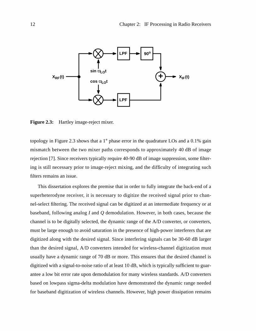
12 Chapter 2: IF Processing in Radio Receivers
topology in Figure2.3 shows that a 1° phase error in the quadrature LOs and a 0.1% gain
mismatch between the two mixer paths corresponds to approximately 40dB of image
rejection [7]. Since receivers typically require 40-90 dB of image suppression, some filter-
ing is still necessary prior to image-reject mixing, and the difficulty of integrating such
filters remains an issue.
This dissertation explores the premise that in order to fully integrate the back-end of a
superheterodyne receiver, it is necessary to digitize the received signal prior to chan-
nel-select filtering. The received signal can be digitized at an intermediate frequency or at
baseband, following analogI andQ demodulation. However, in both cases, because the
channel is to be digitally selected, the dynamic range of the A/D converter, or converters,
must be large enough to avoid saturation in the presence of high-power interferers that are
digitized along with the desired signal. Since interfering signals can be 30-60 dB larger
than the desired signal, A/D converters intended for wireless-channel digitization must
usually have a dynamic range of 70 dB or more. This ensures that the desired channel is
digitized with a signal-to-noise ratio of at least 10 dB, which is typically sufficient to guar-
antee a low bit error rate upon demodulation for many wireless standards. A/D converters
based on lowpass sigma-delta modulation have demonstrated the dynamic range needed
for baseband digitization of wireless channels. However, high power dissipation remains
sin ωLOt
LPF 90o
cos ωLOt
LPF
+ XIF(t)XRF(t)
Figure 2.3: Hartley image-reject mixer.
2.1. Superheterodyne Receiver Architecture 13
an issue in the prototypes reported to date. In one example, a lowpassΣ∆ modulator with a
2-2-2 cascade architecture has been integrated in a 0.72-µm CMOS technology [15]. This
prototype has demonstrated 71dB of peak SNDR and 77dB of dynamic range in a
700-kHz bandwidth with 81mW of power dissipation from a 3.3-V supply. Thus, with
two such A/D converters used in the superheterodyne receiver topology depicted in
Figure2.1, it appears feasible to perform channel-select filtering in the digital domain if
the desired signal has a bandwidth as high as several hundred kHz. Sections2.2 and 2.3
describe two alternative approaches, interleaved IF subsampling and IF digitization, that
can also be used to integrate the back-end circuitry for a superheterodyne receiver. IF dig-
itization is proposed as the method of choice since this technique allows for digital
channel selection and is not susceptible to errors introduced by imperfect analogI andQ
demodulation.
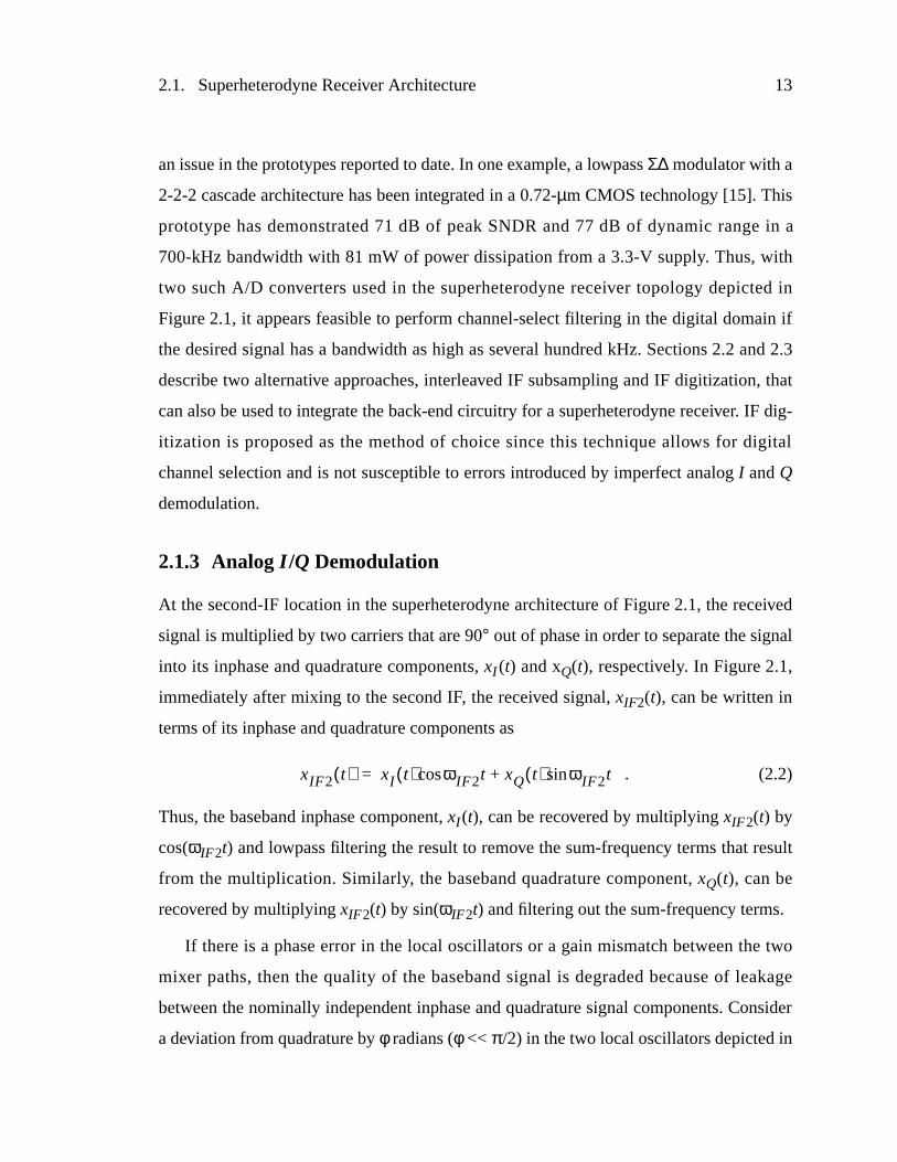
2.1.3 Analog I/Q Demodulation
At the second-IF location in the superheterodyne architecture of Figure2.1, the received
signal is multiplied by two carriers that are 90° out of phase in order to separate the signal
into its inphase and quadrature components,xI (t) and xQ(t), respectively. In Figure2.1,
immediately after mixing to the second IF, the received signal,xIF2(t), can be written in
terms of its inphase and quadrature components as
. (2.2)
Thus, the baseband inphase component,xI (t), can be recovered by multiplyingxIF 2(t) by
cos(ωIF 2t) and lowpass filtering the result to remove the sum-frequency terms that result
from the multiplication. Similarly, the baseband quadrature component,xQ(t), can be
recovered by multiplyingxIF2(t) by sin(ωIF2t) and filtering out the sum-frequency terms.
If there is a phase error in the local oscillators or a gain mismatch between the two
mixer paths, then the quality of the baseband signal is degraded because of leakage
between the nominally independent inphase and quadrature signal components. Consider
a deviation from quadrature byφ radians (φ<< π/2) in the two local oscillators depicted in
xIF2 t( ) xI t( ) ωIF2t xQ t( ) ωIF2tsin+cos=
14 Chapter 2: IF Processing in Radio Receivers
Figure2.4. The degradation in the baseband signal caused by this LO phase error can be
quantified as follows. If the desired signal atfIF2, is a single sinusoid
(2.3)
whereωx << ωIF2, then the output of the inphase channel is
. (2.4)
In (2.4) it has been assumed that a lowpass filter eliminates the sum-frequency term that
results from the mixing operation. With a phase variation,φ, from quadrature in the local
oscillators, the output of the quadrature channel is
. (2.5)
The complex baseband signal,xb(t), is then
cos ωIF2t
LPF
cos ( ωIF2t – (π/2 + φ))
LPF
XIF2(t)
Inphase channel
Quadrature channel
I(t)
Q(t)
≈ sin ωIF2t – φ cos ωIF2t (φ << π/2)
Figure 2.4: AnalogI/Q demodulation with a phase error, φ, in the quadrature localoscillators.
xIF2 t( ) A ωIF2 ωx+( )tcos=
I t( ) A2--- ωxtcos=
Q t( ) A2--- ωxtsin φA
2--- ωxtcos––=
2.1. Superheterodyne Receiver Architecture 15
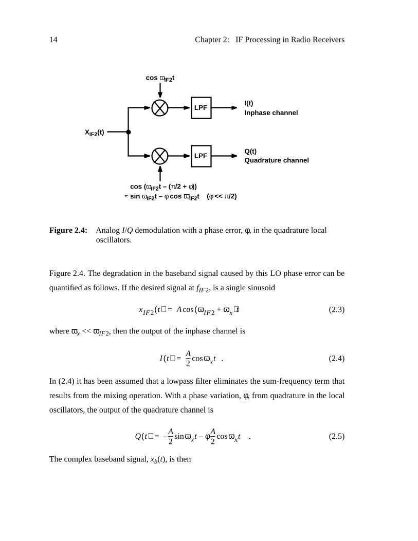
(2.6)
This result indicates thatxb(t) comprises the desired signal, which is a single tone at fre-
quency ωx, together with an error term that contains spectral components atωx and the
mirror frequency, –ωx, as illustrated in Figure2.5. Thus, a phase error between the two
LOs in Figure2.4 results in a mirror signal, also called mirror image, that is a scaled rep-
lica of the desired signal. The degree of mirror-image rejection,IR, is defined as the ratio
of the power of the mirror tone at –ωx to the power of the desired tone atωx and is equal to
A2---= ωxt j ωxtsin+cos( ) jφA
2--- ωxtcos+
A2---e
jωxtjφA
2--- ωxtcos+=
xb t( ) I t( ) jQ t( )–=
.
fIF2–fIF2
f
f
|XIF2(j2πf )|
|Xb(j2πf )|
fx
fx
upon complex
–fx
demodulation with aMirror-ImageRejection
A /2A /2
|A /2 (1 + jφ/2)|
|jφA/4|phase error
Figure 2.5: Frequency spectrum ofxb(t) after analogI/Q demodulation with a phaseerror, φ, between carriers nominally in quadrature.
16 Chapter 2: IF Processing in Radio Receivers
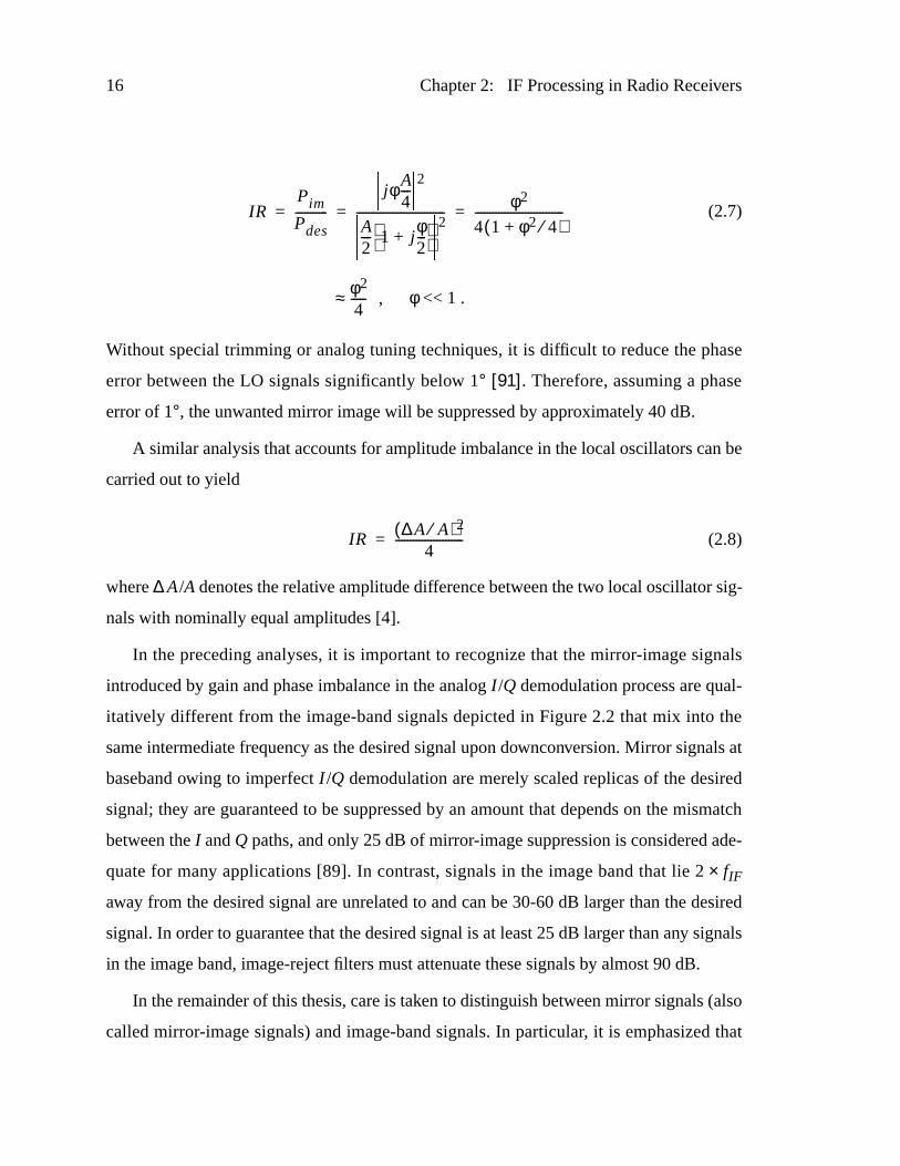
(2.7)
Without special trimming or analog tuning techniques, it is difficult to reduce the phase
error between the LO signals significantly below 1° [91]. Therefore, assuming a phase
error of 1°, the unwanted mirror image will be suppressed by approximately 40 dB.
A similar analysis that accounts for amplitude imbalance in the local oscillators can be
carried out to yield
(2.8)
where∆ A/A denotes the relative amplitude difference between the two local oscillator sig-
nals with nominally equal amplitudes [4].
In the preceding analyses, it is important to recognize that the mirror-image signals
introduced by gain and phase imbalance in the analogI /Q demodulation process are qual-
itatively different from the image-band signals depicted in Figure2.2 that mix into the
same intermediate frequency as the desired signal upon downconversion. Mirror signals at
baseband owing to imperfectI /Q demodulation are merely scaled replicas of the desired
signal; they are guaranteed to be suppressed by an amount that depends on the mismatch
between theI andQ paths, and only 25 dB of mirror-image suppression is considered ade-
quate for many applications [89]. In contrast, signals in the image band that lie 2× fIF
away from the desired signal are unrelated to and can be 30-60 dB larger than the desired
signal. In order to guarantee that the desired signal is at least 25 dB larger than any signals
in the image band, image-reject filters must attenuate these signals by almost 90dB.
In the remainder of this thesis, care is taken to distinguish between mirror signals (also
called mirror-image signals) and image-band signals. In particular, it is emphasized that
IRPim
Pdes-----------
jφA4---
2
A2--- 1 j
φ2---+
2------------------------------ φ2
4 1 φ2 4⁄+( )------------------------------= = =
φ2
4----- ,≈ φ << 1 .
IR∆A A⁄( )2
4-----------------------=
2.2. Interleaved IF Subsampling 17
mirror signals are always scaled replicas of desired signals that typically arise as a result
of circuit mismatches or local oscillator gain and phase imbalances. Signals in the image
band, however, exist independently of the desired signal and can be much larger in power.
In this work, it is assumed that image-band signals are attenuated prior to any frequency
translation from RF to IF, as depicted in Figure2.2. This does not preclude the possibility
of mirror signals arising from nonidealities in a receiver’s back-end circuitry. In the pre-
ceding discussion, imperfect analogI /Q demodulation is shown to be one means by which
a mirror image is generated in the output spectrum of a demodulated signal. An important
and analogous effect, which will be discussed in detail in Chapter 5, results from path mis-
match in anN-path filter.
2.2 Interleaved IF Subsampling
One proposal for reducing the sensitivity of the I /Q demodulation process in a superhet-
erodyne receiver to analog circuit imperfections involves replacing the analog mixers in
the inphase and quadrature branches with a pair of A/D converters that subsample the IF
signal [8]. In effect, subsampling the IF signal performs an equivalent mixing of the signal
down to baseband. A block diagram of a dual-IF receiver with an interleaved subsampling
back-end is depicted in Figure2.6. This receiver’s back-end is comprised of two inter-
leaved, lowpass A/D converters that subsample the second-IF signal,xIF 2(t), at a rate
equal to its carrier frequency, fIF2. Although the sampling frequency is less than twice the
highest frequency component inxIF2(t), destructive aliasing is avoided becausefIF2 is pre-
sumed to be much higher than the bandwidth ofxIF2(t) [59].
If the bandpass signal,xIF2(t), is written in the following general form
, (2.9)
then upon sampling atfs = 1/Ts = ωIF2/2π, the inphase signal,I(t), is
xIF2 t( ) xI t( ) ωIF2tcos xQ t( ) ωIF2tsin+=
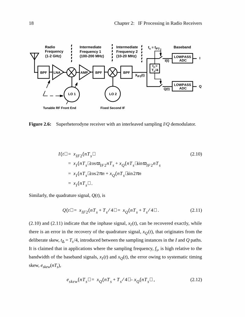
18 Chapter 2: IF Processing in Radio Receivers
(2.10)
Similarly, the quadrature signal,Q(t), is
. (2.11)
(2.10) and (2.11) indicate that the inphase signal,xI (t), can be recovered exactly, while
there is an error in the recovery of the quadrature signal,xQ(t), that originates from the
deliberate skew, t∆ = Ts/4, introduced between the sampling instances in theI andQ paths.
It is claimed that in applications where the sampling frequency, fs, is high relative to the
bandwidth of the baseband signals,xI (t) andxQ(t), the error owing to systematic timing
skew, eskew(nTs),
, (2.12)
IntermediateFrequenc y 1
RadioFrequenc y
LO 1 LO 2
BPF LNA BPF BPFAMP
(1-2 GHz) (100-200 MHz)
IntermediateFrequenc y 2(10-20 MHz)
ADCLOWPASS
ADCLOWPASS
I
Q
Baseband
Tunab le RF Front End Fixed Second IF
t∆=Ts /4
fs = fIF2
XIF2(t)
I(t)
Q(t)
Figure 2.6: Superheterodyne receiver with an interleaved samplingI/Q demodulator.
I t( ) xIF2 nTs( )=
xI nTs( ) ωIF2nTs xQ nTs( ) ωIF2nTssin+cos=
xI nTs( ) 2πn xQ nTs( ) 2πnsin+cos=
xI nTs( )= .
Q t( ) xIF2 nTs Ts 4⁄+( ) xQ nTs Ts 4⁄+( )= =
eskew nTs( ) xQ nTs Ts 4⁄+( ) xQ nTs( )–=
2.3. IF Digitization 19
is negligible [8].
By employing an interleaved subsamplingI /Q demodulator, one set of analog mixers
at the back-end of a superheterodyne receiver can be eliminated, but at the expense of
operating the A/D converters in theI andQ channels at higher sampling speeds. The
resulting increase in power dissipation may be of concern. Furthermore, if the delay
between the sampling clocks,t∆, differs slightly fromTs/4 by an amounte∆, then there
will be a leakage signal between theI andQ channels with a power proportional to .
This leakage results in an incomplete mirror-image suppression that is analogous to mir-
ror-image signals arising from phase and amplitude errors in analogI /Q demodulation.
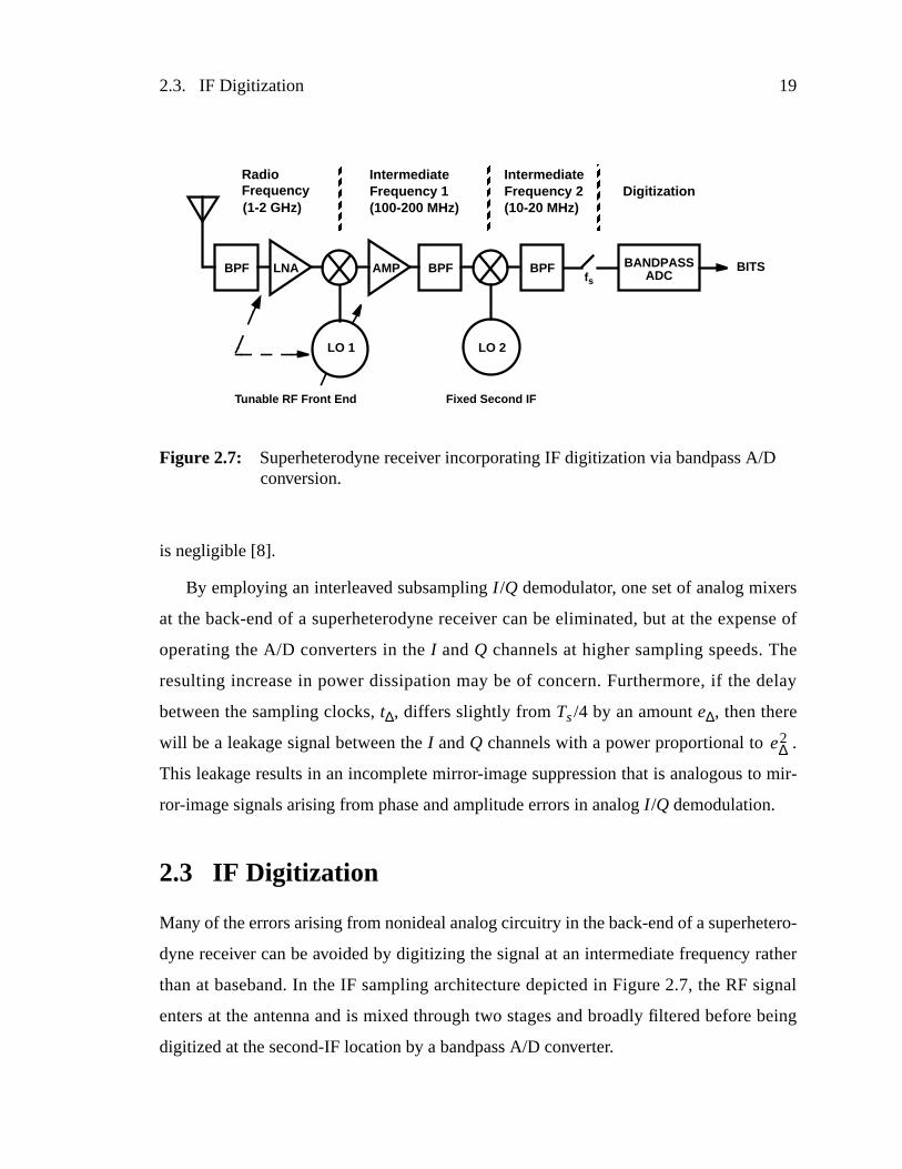
2.3 IF Digitization
Many of the errors arising from nonideal analog circuitry in the back-end of a superhetero-
dyne receiver can be avoided by digitizing the signal at an intermediate frequency rather
than at baseband. In the IF sampling architecture depicted in Figure2.7, the RF signal
enters at the antenna and is mixed through two stages and broadly filtered before being
digitized at the second-IF location by a bandpass A/D converter.
e∆2
IntermediateFrequenc y 1
RadioFrequenc y
LO 1 LO 2
BPF LNA BPF BPFAMP
(1-2 GHz) (100-200 MHz)
IntermediateFrequenc y 2(10-20 MHz)
BITS
Tunab le RF Front End Fixed Second IF
ADCBANDPASS
Digitization
fs
Figure 2.7: Superheterodyne receiver incorporating IF digitization via bandpass A/Dconversion.
20 Chapter 2: IF Processing in Radio Receivers
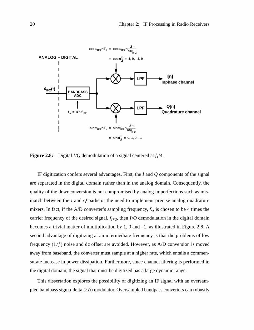
IF digitization confers several advantages. First, theI andQ components of the signal
are separated in the digital domain rather than in the analog domain. Consequently, the
quality of the downconversion is not compromised by analog imperfections such as mis-
match between theI andQ paths or the need to implement precise analog quadrature
mixers. In fact, if the A/D converter’s sampling frequency, fs, is chosen to be 4 times the
carrier frequency of the desired signal,fIF2, thenI /Q demodulation in the digital domain
becomes a trivial matter of multiplication by 1,0 and–1, as illustrated in Figure2.8. A
second advantage of digitizing at an intermediate frequency is that the problems of low
frequency (1/ f ) noise and dc offset are avoided. However, as A/D conversion is moved
away from baseband, the converter must sample at a higher rate, which entails a commen-
surate increase in power dissipation. Furthermore, since channel filtering is performed in
the digital domain, the signal that must be digitized has a large dynamic range.
This dissertation explores the possibility of digitizing an IF signal with an oversam-
pled bandpass sigma-delta (Σ∆) modulator. Oversampled bandpass converters can robustly
Figure 2.8: Digital I /Q demodulation of a signal centered atfs/4.
LPF
LPF
XIF2(t)
Inphase channel
Quadrature channel
I[n]
Q[n]
ωIF2nTscos ωIF2n2π
4ωIF2
---------------cos=
nπ2---cos 1 0 1 0,–, ,= =
ωIF2sin nTs ωIF2sin n2π
4ωIF2
---------------=
nsinπ2--- 0 1 0 1–, , ,= =
ADCBANDPASS
fs 4 f IF2×=
ANALOG – DIGITAL
2.4. Summary 21
digitize the types of narrowband IF signals that arise in radios and cellular systems [50],
[55], [56], [66]-[71]. Moreover, a receiver back-end that employs oversampled bandpass
Σ∆ modulation is easily integrated because such converters can achieve the large dynamic
range necessary for wireless systems without requiring trimming, or other steps incompat-
ible with a standard, low-cost, CMOS process. However, in many such converters, the
sampling frequency of the modulator is often restricted to be exactly four times the pass-
band frequency. The architectural issues underlying this design choice are discussed in
detail in the following chapters, but it can be noted immediately that the dynamic range of
an fs/4 bandpass A/D converter becomes increasingly constrained by circuit nonidealities
at the high sampling rates needed to digitize signals at IF locations above 10 MHz. Conse-
quently, for applications requiring a dynamic range of 70 dB or greater, the signal
passband in previously reportedfs/4 modulators, has been located at a relatively low IF
(under 5 MHz) [55], [69]. The emphasis in this research is to explore the performance lim-
its of bandpassΣ∆ modulators at high sampling speeds such that narrowband (<200 kHz)
IF signals centered as high as 20 MHz can be digitized with over 70 dB of dynamic range.
2.4 Summary
This chapter has examined selectivity and integration issues in the back-end of a conven-
tional superheterodyne radio receiver. Traditional fixed-frequency, highly-selective IF
channel-select filters are seen to be a bottleneck inhibiting the full integration of the
back-end of such a receiver. It is proposed that digitizing the signal at an intermediate fre-
quency and implementing channel filtering in the digital domain is an effective means to
circumvent this limitation. Previously reported lowpass A/D converters based onΣ∆ mod-
ulation have demonstrated the dynamic range needed to digitize baseband signals prior to
channel filtering. However, in this approach, the quality of the baseband signal is suscepti-
ble to imperfections in the analogI /Q demodulation process. IF digitization by means of
bandpass sigma-delta modulation is proposed as an alternative method that allows for the
received signal to be digitized with a large dynamic range. Furthermore, in certain cases,

22 Chapter 2: IF Processing in Radio Receivers
the subsequent digitalI /Q demodulation can be implemented in a trivial manner that only
requires multiplication by 1, 0 and –1. The next chapter reviews the principles of bandpass
Σ∆ modulation.
23
Chapter
3 Bandpass Σ∆Modulation
Digitization of the intermediate-frequency (IF) signal in a radio receiver can typically be
accomplished with either a wideband Nyquist-rate analog-to-digital (A/D) converter or a
converter that utilizes oversampling techniques and a noiseshaping architecture. Because
the digitization of the IF signal is performed prior to channel-select filtering, the A/D con-
verter must have a wide dynamic range in order to handle potential interferers, which may
be 30-60 dB higher than the desired signal. Consequently, depending on the specifications
of the particular wireless standard and the receiver architecture, the A/D converter may be
required to have a dynamic range of 70 dB or greater.
It is problematic to design high-precision data converters with a traditional
Nyquist-rate architecture in a modern submicron VLSI technology. Although submicron
VLSI processes confer the benefits of smaller devices, increased transistor density, multi-
ple layers of metal, and gate speeds on the order of tens of picoseconds, analog designs are
encumbered because the process is optimized for digital circuits rather than precision
mixed-signal analog applications. Due to short-channel effects and limitations imposed by
velocity saturation, the intrinsic gain of the devices,gmro, may be poor and the devices
may be inherently noisier than their long-channel counterparts [99]. Often, these charac-
teristics are poorly reflected in the models of the devices, which may then be inadequate
for analog design. The designer may also be constrained by reduced supply voltages that
preclude the use of certain analog circuit topologies such as cascoded amplifiers.
It is possible to utilize oversampling and noiseshaping principles to overcome the
inherent limitations of the devices in a VLSI process. Noiseshaping techniques for wave-
24 Chapter 3: BandpassΣ∆ Modulation
form coding, with early applications to voiceband telecom, video encoders, and satellite
telemetry, have been in existence since the early 1960s [9]-[11]. Through oversampling,
feedback, and digital filtering, resolution in time is exchanged for that in amplitude.
Therefore, it is possible to achieve a high dynamic range in spite of the poor device match-
ing typical in VLSI processes. However, it was not feasible to implement a
fully-integrated A/D converter in this manner until the late 1970s and early 1980s, when
the density of CMOS technologies had improved to the point where the digital processing
required became economical. The performance of noiseshaping converters has continued
to increase with the scaling of VLSI technology, allowing them to progress through the
increasingly demanding specifications of voiceband telecom, digital audio, ISDN, and
channel digitization in wireless receivers [12]-[15].
In the past several years, the concept of lowpass noiseshaping has been extended to the
bandpass regime whereby a narrowband signal centered around an intermediate frequency
is directly digitized without first mixing the signal down to baseband [16], [17]. Through
the design of an appropriate noise transfer function, the signal passband can be positioned
at any location within the sampling bandwidth, –fs/2 to fs/2. In fact, certain classes offs/4
modulators are easily derived from existing lowpass topologies by applying a simple
mathematical transformation to be described in Section3.3.2. The simplicity of this
approach is a strong motivation for adopting an architecture based upon a dc-to-fs/4 trans-
formation. However, system-level optimization with respect to factors such as spectral
coloration and overload performance may demand more degrees of freedom than allowed
by the transformation process. In addition, an unreasonably high sampling rate may be
imposed on the analog circuitry if the modulator is to digitize a signal passband that is
centered in the tens of MHz. These architectural issues are explored in depth in this
chapter.
Before proceeding to a detailed discussion of bandpass sigma-delta (Σ∆) modulation, a
fundamental review of analog-to-digital conversion is presented, which is followed by an
overview of oversampling and noiseshaping A/D techniques. Then, the remainder of the
chapter is devoted to a broad study of bandpass noiseshaping architectures and a survey of
3.1. Nyquist-rate A/D Converters 25
design methodologies. Transformations that operate on a lowpass prototype are discussed,
and a generalized design technique that directly synthesizes the desired noiseshaping
function is presented.
3.1 Nyquist-rate A/D Converters
Analog-to-digital conversion is the process of encoding an analog signal that is continuous
in time and amplitude into a signal that is discrete with respect to time and quantized in
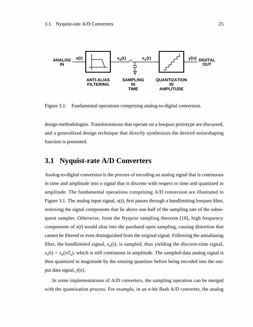
amplitude. The fundamental operations comprising A/D conversion are illustrated in
Figure3.1. The analog input signal,x(t), first passes through a bandlimiting lowpass filter,
removing the signal components that lie above one-half of the sampling rate of the subse-
quent sampler. Otherwise, from the Nyquist sampling theorem [18], high frequency
components ofx(t) would alias into the passband upon sampling, causing distortion that
cannot be filtered or even distinguished from the original signal. Following the antialiasing
filter, the bandlimited signal,xa(t), is sampled, thus yielding the discrete-time signal,
xs(t) = xa(nTs), which is still continuous in amplitude. The sampled-data analog signal is
then quantized in magnitude by the ensuing quantizer before being encoded into the out-
put data signal,y[n].
In some implementations of A/D converters, the sampling operation can be merged
with the quantization process. For example, in ann-bit flash A/D converter, the analog
Figure3.1: Fundamental operations comprising analog-to-digital conversion.
ANTI-ALIASFILTERING
SAMPLINGIN
TIME
QUANTIZATIONIN
AMPLITUDE
ANALOGIN
DIGITALOUT
x(t) xa(t) xs(t) y [n]
26 Chapter 3: BandpassΣ∆ Modulation
input signal is simultaneously compared to 2n–1 reference voltages in a fully-parallel
operation. Thus, in principle, flash A/D converters do not need to sample the signal prior
to quantization because the sampling process can be performed implicitly by strobing a
comparator bank.
3.1.1 Sampling
From the Nyquist sampling theorem, if there is to be no loss of information or aliasing dis-
tortion upon sampling,x(t) must be sampled at a frequency higher than twice the baseband
cutoff frequency, fb, which is defined as the cutoff frequency for the antialiasing filter as
shown in Figure3.2. In the frequency domain, the spectrum of the sampled signal,xs(t), is
. (3.1)
If the sampling frequency, fs, is chosen to be at, or slightly higher than, the Nyquist
rate, 2fb, then the converter is said to be aNyquist-rate converter. However, the sampling
rate can deliberately be chosen to greatly exceed the Nyquist rate in order to exploit the
benefits of oversampling, to be described later in this chapter. In this case, the converter is
referred to as anoversampling converter. When the passband extends from dc tofb, the
oversampling ratio,M, is defined asM = fs/(2 × fb), with M = 1 for a Nyquist-rate con-
verter. The two classes of sampling are depicted in Figure3.2.
3.1.2 Quantization
In principle, the sampling process does not result in any loss of information, provided that
the sampling rate exceeds the Nyquist rate. However, this is not true of the quantization of
the sampled signal because, in this non-reversible operation, a continuous range of ampli-
tudes is mapped into a finite set of digital output codes. The transfer characteristic of a
uniform quantizer with a gain of unity is illustrated in Figure3.3(a), and the resulting saw-
Xs f( ) 1Ts----- Xa f k f s–( )
k ∞–=
∞
∑=
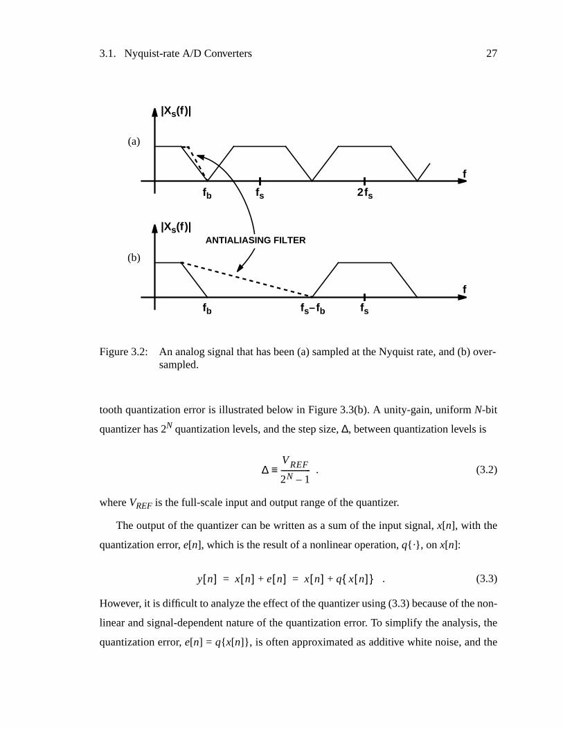
3.1. Nyquist-rate A/D Converters 27
tooth quantization error is illustrated below in Figure3.3(b). A unity-gain, uniformN-bit
quantizer has 2N quantization levels, and the step size,∆, between quantization levels is
. (3.2)
whereVREF is the full-scale input and output range of the quantizer.
The output of the quantizer can be written as a sum of the input signal,x[n], with the
quantization error, e[n], which is the result of a nonlinear operation,q·, on x[n]:
. (3.3)
However, it is difficult to analyze the effect of the quantizer using (3.3) because of the non-
linear and signal-dependent nature of the quantization error. To simplify the analysis, the
quantization error, e[n] = q x[n], is often approximated as additive white noise, and the
Figure3.2: An analog signal that has been (a) sampled at the Nyquist rate, and (b) over-sampled.
fb fs 2fs
fs
ANTIALIASING FILTER
fb fs–fb
f
f
|Xs(f )|
|Xs(f )|
(a)
(b)
∆VREF
2N 1–----------------≡
y n[ ] x n[ ] e n[ ]+ x n[ ] q x n[ ] += =
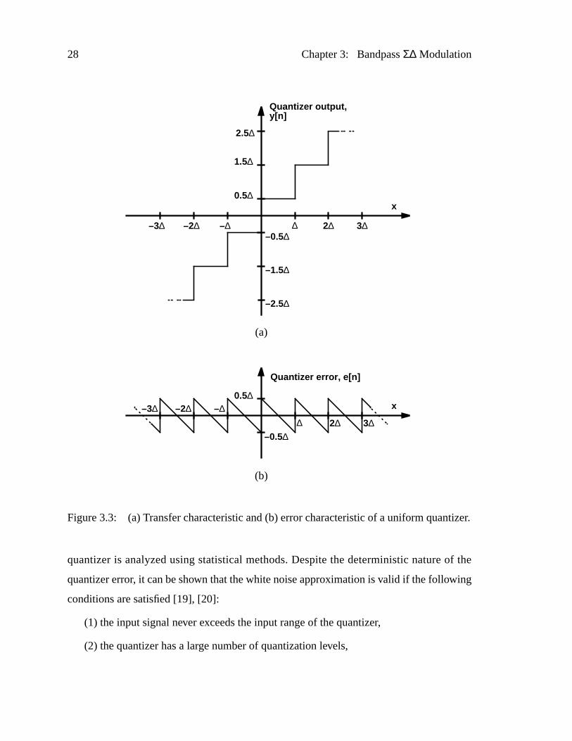
28 Chapter 3: BandpassΣ∆ Modulation
quantizer is analyzed using statistical methods. Despite the deterministic nature of the
quantizer error, it can be shown that the white noise approximation is valid if the following
conditions are satisfied [19], [20]:
(1) the input signal never exceeds the input range of the quantizer,
(2) the quantizer has a large number of quantization levels,
Figure3.3: (a) Transfer characteristic and (b) error characteristic of a uniform quantizer.
∆ 2∆ 3∆–∆–2∆–3∆
0.5∆
1.5∆
–0.5∆
–1.5∆
x
Quantizer output,
∆ 2∆ 3∆–∆–2∆–3∆
0.5∆
–0.5∆
Quantizer error, e[n]
(a)
(b)
y[n]
x
2.5∆
–2.5∆
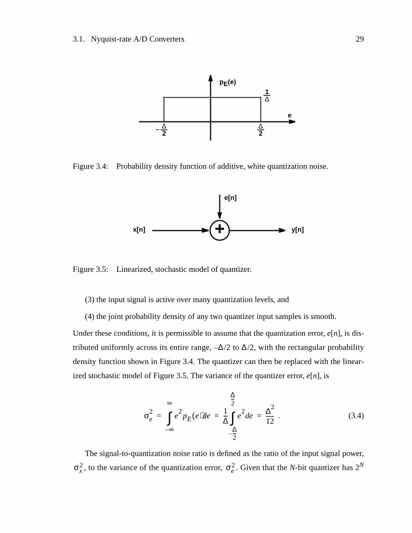
3.1. Nyquist-rate A/D Converters 29
(3) the input signal is active over many quantization levels, and
(4) the joint probability density of any two quantizer input samples is smooth.
Under these conditions, it is permissible to assume that the quantization error, e[n], is dis-
tributed uniformly across its entire range, –∆ /2 to ∆ /2, with the rectangular probability
density function shown in Figure3.4. The quantizer can then be replaced with the linear-
ized stochastic model of Figure3.5. The variance of the quantizer error, e[n], is
. (3.4)
The signal-to-quantization noise ratio is defined as the ratio of the input signal power,
, to the variance of the quantization error, . Given that theN-bit quantizer has 2N
Figure3.4: Probability density function of additive, white quantization noise.
∆2
∆2
–
1∆
e
pE(e)
Figure3.5: Linearized, stochastic model of quantizer.
+x[n]
e[n]
y[n]
σe2
e2pE e( ) ed
∞–
∞
∫ 1∆--- e
2ed
∆2---–
∆2---
∫ ∆2
12------= = =
σx2 σe
2
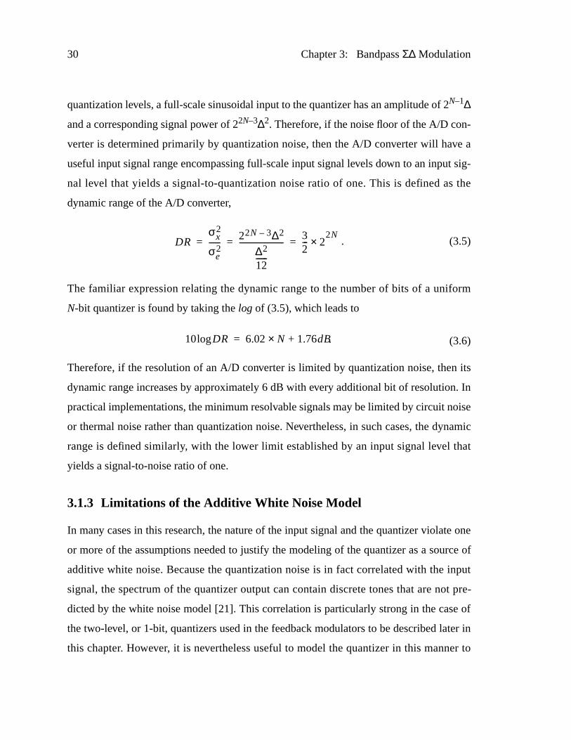
30 Chapter 3: BandpassΣ∆ Modulation
quantization levels, a full-scale sinusoidal input to the quantizer has an amplitude of 2N–1∆
and a corresponding signal power of 22N–3∆2. Therefore, if the noise floor of the A/D con-
verter is determined primarily by quantization noise, then the A/D converter will have a
useful input signal range encompassing full-scale input signal levels down to an input sig-
nal level that yields a signal-to-quantization noise ratio of one. This is defined as the
dynamic range of the A/D converter,
. (3.5)
The familiar expression relating the dynamic range to the number of bits of a uniform
N-bit quantizer is found by taking thelog of (3.5), which leads to
(3.6)
Therefore, if the resolution of an A/D converter is limited by quantization noise, then its
dynamic range increases by approximately 6 dB with every additional bit of resolution. In
practical implementations, the minimum resolvable signals may be limited by circuit noise
or thermal noise rather than quantization noise. Nevertheless, in such cases, the dynamic
range is defined similarly, with the lower limit established by an input signal level that
yields a signal-to-noise ratio of one.
3.1.3 Limitations of the Additi ve White Noise Model
In many cases in this research, the nature of the input signal and the quantizer violate one
or more of the assumptions needed to justify the modeling of the quantizer as a source of
additive white noise. Because the quantization noise is in fact correlated with the input
signal, the spectrum of the quantizer output can contain discrete tones that are not pre-
dicted by the white noise model [21]. This correlation is particularly strong in the case of
the two-level, or 1-bit, quantizers used in the feedback modulators to be described later in
this chapter. However, it is nevertheless useful to model the quantizer in this manner to
DRσx
2
σe2
------ 22N 3– ∆2
∆2
12------
------------------------32--- 2×
2N= = =
10 DRlog 6.02 N× 1.76dB+= .
3.1. Nyquist-rate A/D Converters 31
predict the performance of an A/D converter, despite the failure of the system to adhere to
the stipulations of the model. In particular, even though the 1-bit quantizer violates the
conditions of the model, the white noise quantizer model still allows for an accurate esti-
mate of the dynamic range of a modulator that is comprised essentially of a 1-bit quantizer
embedded in a feedback loop. In such cases, the only justification for modeling the quan-
tizer as an additive white noise source is that behavioral simulations of the system confirm
the estimate of the dynamic range arrived at with the use of this model.
3.1.4 Limitations of Nyquist-Rate A/D Converters
There are many architectures for Nyquist-rate A/D converters, each of which embodies
various tradeoffs among bandwidth, power dissipation, area, and dynamic range require-
ments. A thorough review of many architectures is presented in [22], [23]. A common
limiting factor in all Nyquist-rate architectures is that some operation such as comparison,
amplification, or subtraction must be performed to the overall precision of the converter.
This typically translates into the need for precise component matching unless special cali-
bration, error-correction, or trimming techniques are used, with attendant penalties in die
area, power dissipation, or manufacturing cost. With careful layout techniques, matching
of 0.3% can be routinely achieved in modern CMOS processes, and matching as good as
0.1% has been observed [30]. However, it is important to note that even with 0.1% match-
ing, the resolution of an uncalibrated and untrimmed Nyquist-rate converter is limited to
only 10 bits.
A steep antialiasing filter must also precede any Nyquist-rate A/D converter. This
bandlimiting filter rejects frequency components of the signal located above one-half of
the sampling frequency in order to prevent aliasing distortion. However, to allow for a
large signal bandwidth, the filter’s stopband corner frequency must also be near one-half
of the sampling frequency. Thus, as depicted in Figure3.2(a), the antialiasing filter must
have a sharp transition band, which typically introduces phase distortion in signal compo-
nents located near the cutoff frequency. Furthermore, it is difficult to implement precise
analog filters with multiple poles in a VLSI technology due to a lack of high-Q inductors
32 Chapter 3: BandpassΣ∆ Modulation
and well-defined, stable resistor and capacitor values. Circuit noise and distortion in active
implementations of continuous-time filters, such asgm/C topologies, often limit their util-
ity to applications that only require a low- to medium dynamic range [24]-[29]. This
becomes increasingly true at the low supply voltages, 2.5 V to 3.3 V, typical of submicron
technologies, in which the large signal swings necessary for a high dynamic range directly
conflict with the linearity requirements of the filter. Finally, the precisely defined poles and
zeros of any high-order continuous time filter will be subjected to a wide range of environ-
mental and processing fluctuations that can potentially disturb the passband response and
degrade the sharp selectivity of the filter. Thus, a compensatory automatic tuning scheme
may be necessary to constrain the variations of the filter’s frequency response [29].
3.2 Oversampled A/D Converters
By exploiting the speed of a VLSI technology, it is often possible to sample the input sig-
nal at a rate much higher than the Nyquist rate. This oversampling offers the immediate
advantage of relaxing the requirement for a steep transition band on the antialiasing filter,
as illustrated in Figure3.2(b). However, as discussed in the following section, oversam-
pling by itself leads to only modest improvements in resolution of the converter. If the
quantizer is also embedded in a feedback loop, it is possible to significantly increase the
resolution of a converter beyond what can be achieved simply by oversampling.
It is important to note that the quantization process in an oversampled converter
employing feedback differs fundamentally from that in a Nyquist-rate converter. It is not
necessary to quantize the signal in an oversampled converter to the full resolution of the
converter because each sample of the input signal does not correspond to only one output
sample. Rather, in the digital filter that follows the oversampled converter, many coarsely
quantized samples are processed to yield a more precise estimate of the analog input sig-
nal at a lower sampling rate. Thus, each output sample depends on a long sequence of
input samples. In many cases, single-bit quantization is sufficient in an oversampled feed-
back modulator.
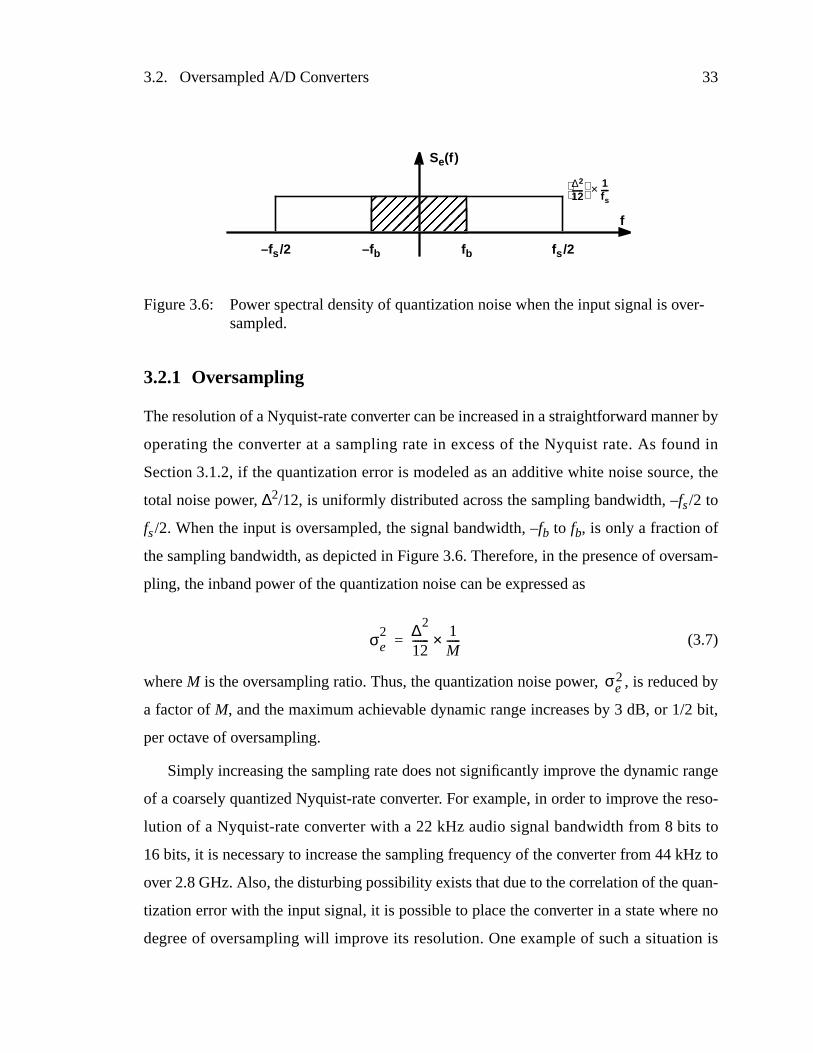
3.2. Oversampled A/D Converters 33
3.2.1 Oversampling
The resolution of a Nyquist-rate converter can be increased in a straightforward manner by
operating the converter at a sampling rate in excess of the Nyquist rate. As found in
Section3.1.2, if the quantization error is modeled as an additive white noise source, the
total noise power, ∆2/12, is uniformly distributed across the sampling bandwidth, –fs/2 to
fs/2. When the input is oversampled, the signal bandwidth, –fb to fb, is only a fraction of
the sampling bandwidth, as depicted in Figure3.6. Therefore, in the presence of oversam-
pling, the inband power of the quantization noise can be expressed as
(3.7)
whereM is the oversampling ratio. Thus, the quantization noise power, , is reduced by
a factor ofM, and the maximum achievable dynamic range increases by 3 dB, or 1/2 bit,
per octave of oversampling.
Simply increasing the sampling rate does not significantly improve the dynamic range
of a coarsely quantized Nyquist-rate converter. For example, in order to improve the reso-
lution of a Nyquist-rate converter with a 22 kHz audio signal bandwidth from 8bits to
16bits, it is necessary to increase the sampling frequency of the converter from 44kHz to
over 2.8 GHz. Also, the disturbing possibility exists that due to the correlation of the quan-
tization error with the input signal, it is possible to place the converter in a state where no
degree of oversampling will improve its resolution. One example of such a situation is
σe2 ∆2
12------ 1
M-----×=
Figure3.6: Power spectral density of quantization noise when the input signal is over-sampled.
Se(f )
f
fs /2–fs /2 fb–fb
∆2
12------
1fs----×
σe2
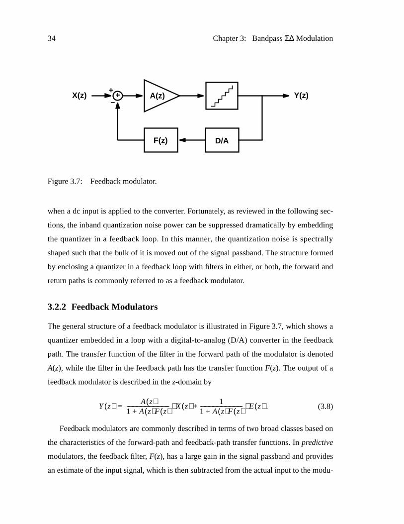
34 Chapter 3: BandpassΣ∆ Modulation
when a dc input is applied to the converter. Fortunately, as reviewed in the following sec-
tions, the inband quantization noise power can be suppressed dramatically by embedding
the quantizer in a feedback loop. In this manner, the quantization noise is spectrally
shaped such that the bulk of it is moved out of the signal passband. The structure formed
by enclosing a quantizer in a feedback loop with filters in either, or both, the forward and
return paths is commonly referred to as a feedback modulator.
3.2.2 Feedback Modulators
The general structure of a feedback modulator is illustrated in Figure3.7, which shows a
quantizer embedded in a loop with a digital-to-analog (D/A) converter in the feedback
path. The transfer function of the filter in the forward path of the modulator is denoted
A(z), while the filter in the feedback path has the transfer functionF(z). The output of a
feedback modulator is described in thez-domain by
. (3.8)
Feedback modulators are commonly described in terms of two broad classes based on
the characteristics of the forward-path and feedback-path transfer functions. Inpredictive
modulators, the feedback filter, F(z), has a large gain in the signal passband and provides
an estimate of the input signal, which is then subtracted from the actual input to the modu-
Figure3.7: Feedback modulator.
+X(z) Y(z)+–
A(z)
F(z) D/A
Y z( ) A z( )1 A z( )F z( )+-------------------------------- X z( ) 1
1 A z( )F z( )+-------------------------------- E z( )⋅+⋅=
3.2. Oversampled A/D Converters 35
lator, X(z). If the predicted value is close to the input value, the quantizer input will be
small, allowing the use of a quantizer with a small input range. In effect, by encoding the
rate of change of a signal rather than the signal itself, apredictive modulator can employ a
quantizer with a small step size and a commensurately small quantization error. In con-
trast,noiseshaping modulators do not reduce the magnitude of the quantization noise.
Instead, a large frequency-dependent gain in the forward path,A(z), is used to spectrally
shape the quantization noise and suppress it in the signal passband. Most of the power in
the quantization noise is moved into the stopband where it is removed by a digital filter
that follows the modulator.
In a predictive modulator, both the input signal and the quantization noise undergo
spectral shaping [31]-[34]. This fact has important implications in the practical implemen-
tation of feedback modulators. From (3.8) it is seen that the signal transfer function,
STF(z), of a feedback modulator is
. (3.9)
Since the passband gain of the feedback filter, F(z), is very high in a predictive modulator,
the signal transfer function is approximately 1/F(z). Therefore, the digital filter that fol-
lows a predictive modulator must apply an inverse transfer function, , which is a
digital approximation of the analog feedback filter transfer functionF(z), to the output of
the modulator in order to recover the input signal. Mismatch between andF(z) pre-
sents an immediate limitation because the nonidealities in the analog circuits that are the
root cause of the mismatch cannot be predicteda priori. Furthermore, mismatch-related
errors are greatly amplified because the passband gain ofF(z) and is very high.
In noiseshaping modulators, only the quantization noise is spectrally shaped [13], [14],
[35]-[37]. The forward filter, A(z), has a large passband gain and the feedback filter, F(z),
is independent of frequency in the passband. Therefore, the signal transfer function, (3.9),
reduces to a constant in the passband, and the digital filter that follows a noiseshaping
modulator must only reject the large, out-of-band quantization noise without altering the
STF z( ) A z( )1 A z( )F z( )+--------------------------------=
F z( )
F z( )
F z( )
36 Chapter 3: BandpassΣ∆ Modulation
frequency response in the signal passband. The performance of a noiseshaping modulator
is not limited by the need to match a digital decoding filter , to the analog feedback
filter, F(z), in the modulator. For this reason,noiseshaping topologies are preferred if the
feedback modulator is to be implemented with analog circuitry. This research work
focuses exclusively on noiseshaping topologies.
At this point, it is important to note that in the development of noiseshaping techniques
it was usually presumed that the signal passband was situated at baseband. However, spec-
tral shaping of noise is not restricted to the lowpass domain. Rather, through an
appropriate choice of the forward and feedback transfer functions,A(z) andF(z), it is pos-
sible to shape the bulk of the quantization noise power away from any region in the
sampling bandwidth, –fs/2 to fs/2. The concept of bandpass noiseshaping will be devel-
oped later in this chapter following the initial discussion of lowpass noiseshaping.
3.2.3 Lowpass Sigma-Delta (Σ∆) Modulation
In noiseshaping topologies, the forward path filter is designed to have a large gain in the
passband in which the quantization noise is to be suppressed. From Figure3.7, it follows
that if F(z) is chosen to be 1, thez-domain expression for the output can written as
(3.10)
whereX(z) andE(z) are thez-transforms of the input signal and quantization error, respec-
tively. Therefore, if the quantization noise is to be suppressed in the baseband,A(z) must
have a large dc gain. There are many transfer functions that satisfy this condition and
could be used to implement a noiseshaping modulator, but one class of transfer functions
comprised of integrators is especially suited for VLSI implementation because the analog
circuits required to implement the transfer function are simple and robust.
A z-domain representation of a first-orderΣ∆ modulator is depicted in Figure3.8. The
modulator is comprised of a subtraction node, a discrete-time integrator, and a 1-bit quan-
tizer. The quantization noise is represented by the additive term,E(z). The integrator
F z( )
Y z( ) A z( )1 A z( )+-------------------- X z( ) 1
1 A z( )+-------------------- E z( )⋅+⋅=
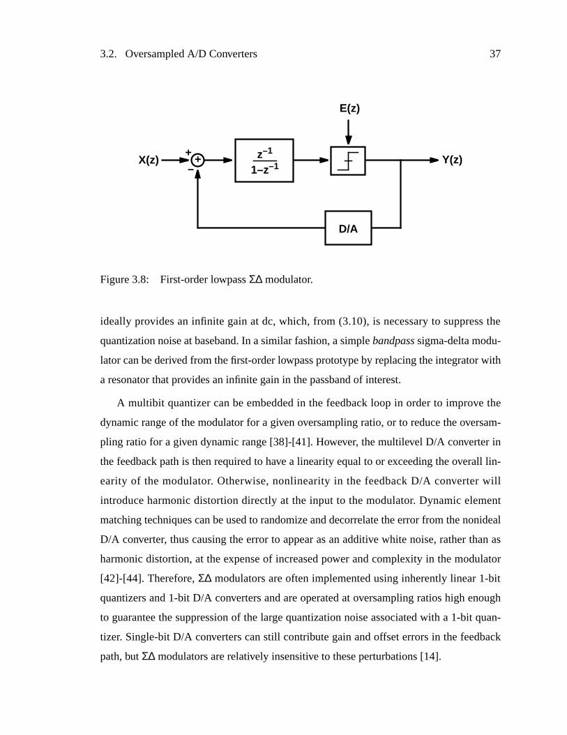
3.2. Oversampled A/D Converters 37
ideally provides an infinite gain at dc, which, from (3.10), is necessary to suppress the
quantization noise at baseband. In a similar fashion, a simplebandpass sigma-delta modu-
lator can be derived from the first-order lowpass prototype by replacing the integrator with
a resonator that provides an infinite gain in the passband of interest.
A multibit quantizer can be embedded in the feedback loop in order to improve the
dynamic range of the modulator for a given oversampling ratio, or to reduce the oversam-
pling ratio for a given dynamic range [38]-[41]. However, the multilevel D/A converter in
the feedback path is then required to have a linearity equal to or exceeding the overall lin-
earity of the modulator. Otherwise, nonlinearity in the feedback D/A converter will
introduce harmonic distortion directly at the input to the modulator. Dynamic element
matching techniques can be used to randomize and decorrelate the error from the nonideal
D/A converter, thus causing the error to appear as an additive white noise, rather than as
harmonic distortion, at the expense of increased power and complexity in the modulator
[42]-[44]. Therefore,Σ∆ modulators are often implemented using inherently linear 1-bit
quantizers and 1-bit D/A converters and are operated at oversampling ratios high enough
to guarantee the suppression of the large quantization noise associated with a 1-bit quan-
tizer. Single-bit D/A converters can still contribute gain and offset errors in the feedback
path, but Σ∆ modulators are relatively insensitive to these perturbations [14].
Figure3.8: First-order lowpassΣ∆ modulator.
+X(z) Y(z)+–
E(z)
z–1
1–z–1
D/A
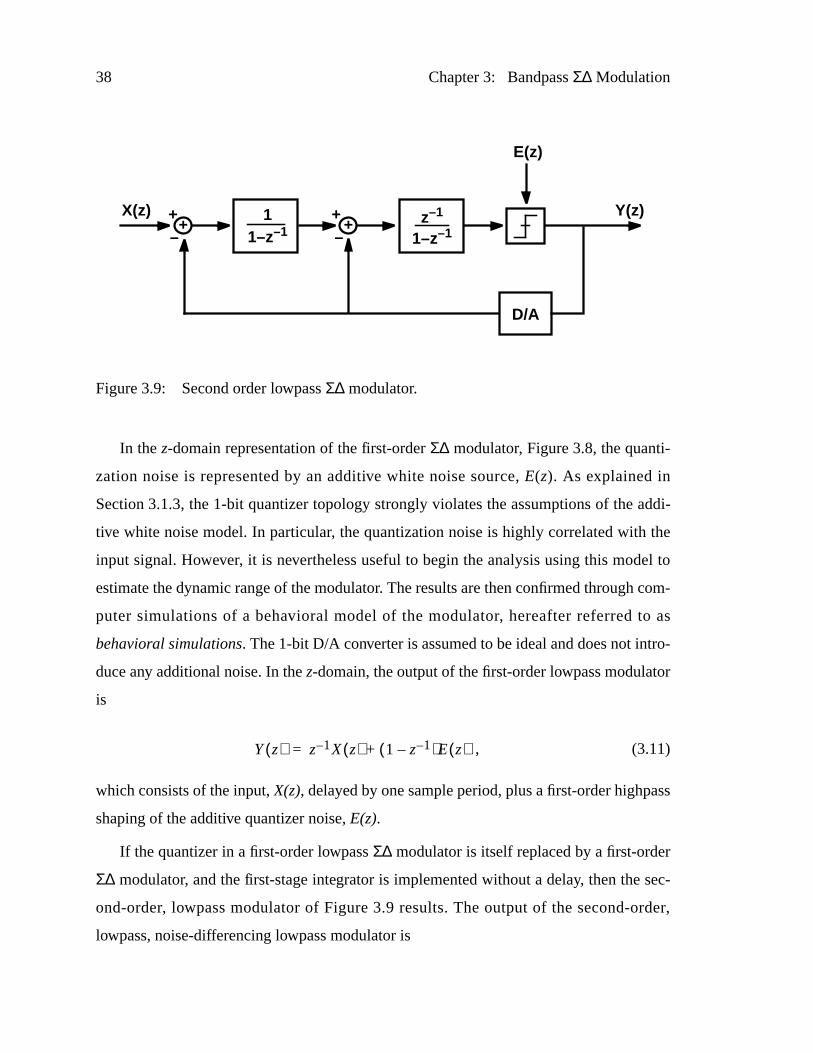
38 Chapter 3: BandpassΣ∆ Modulation
In thez-domain representation of the first-orderΣ∆ modulator, Figure3.8, the quanti-
zation noise is represented by an additive white noise source,E(z). As explained in
Section3.1.3, the 1-bit quantizer topology strongly violates the assumptions of the addi-
tive white noise model. In particular, the quantization noise is highly correlated with the
input signal. However, it is nevertheless useful to begin the analysis using this model to
estimate the dynamic range of the modulator. The results are then confirmed through com-
puter simulations of a behavioral model of the modulator, hereafter referred to as
behavioral simulations. The 1-bit D/A converter is assumed to be ideal and does not intro-
duce any additional noise. In thez-domain, the output of the first-order lowpass modulator
is
, (3.11)
which consists of the input,X(z), delayed by one sample period, plus a first-order highpass
shaping of the additive quantizer noise,E(z).
If the quantizer in a first-order lowpassΣ∆ modulator is itself replaced by a first-order
Σ∆ modulator, and the first-stage integrator is implemented without a delay, then the sec-
ond-order, lowpass modulator of Figure3.9 results. The output of the second-order,
lowpass, noise-differencing lowpass modulator is
Y z( ) z 1– X z( ) 1 z 1––( )E z( )+=
Figure3.9: Second order lowpassΣ∆ modulator.
+X(z) Y(z)+
–
D/A
E(z)
11–z–1 +
+–
z–1
1–z–1
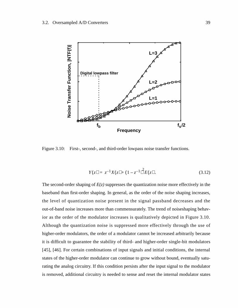
3.2. Oversampled A/D Converters 39
. (3.12)
The second-order shaping ofE(z) suppresses the quantization noise more effectively in the
baseband than first-order shaping. In general, as the order of the noise shaping increases,
the level of quantization noise present in the signal passband decreases and the
out-of-band noise increases more than commensurately. The trend of noiseshaping behav-
ior as the order of the modulator increases is qualitatively depicted in Figure3.10.
Although the quantization noise is suppressed more effectively through the use of
higher-order modulators, the order of a modulator cannot be increased arbitrarily because
it is difficult to guarantee the stability of third- and higher-order single-bit modulators
[45], [46]. For certain combinations of input signals and initial conditions, the internal
states of the higher-order modulator can continue to grow without bound, eventually satu-
rating the analog circuitry. If this condition persists after the input signal to the modulator
is removed, additional circuitry is needed to sense and reset the internal modulator states
Y z( ) z 1– X z( ) 1 z 1––( )2E z( )+=
Noi
se T
rans
fer
Fun
ctio
n, |N
TF
(f)|
Frequency
L=3
L=2
L=1
fs /2
Digital lowpass filter
fb
Figure3.10: First-, second-, and third-order lowpass noise transfer functions.
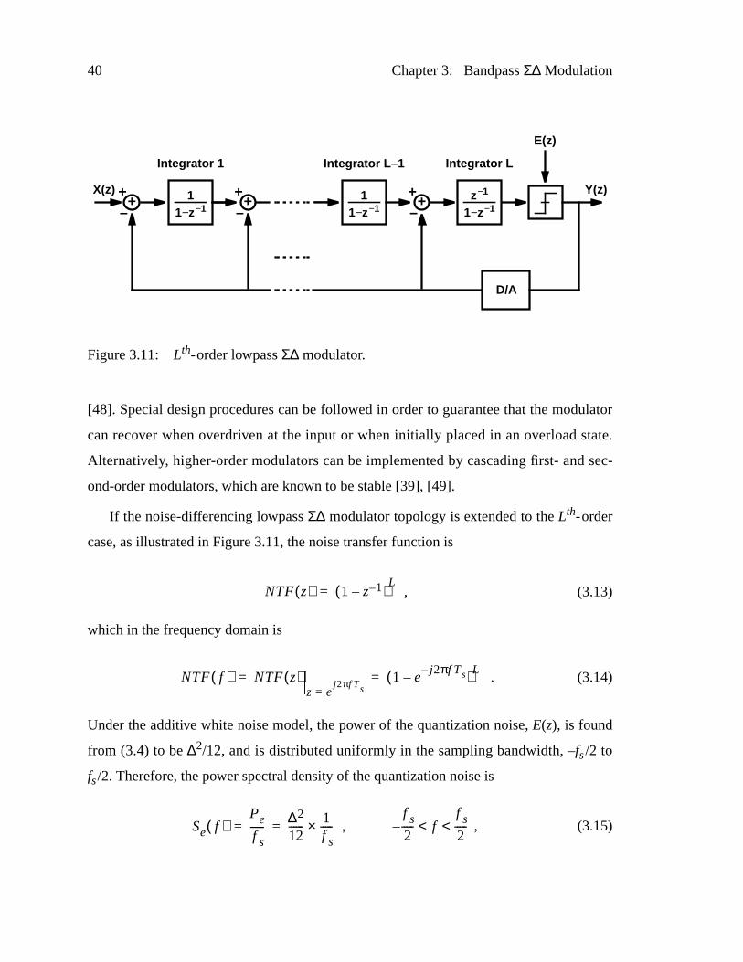
40 Chapter 3: BandpassΣ∆ Modulation
[48]. Special design procedures can be followed in order to guarantee that the modulator
can recover when overdriven at the input or when initially placed in an overload state.
Alternatively, higher-order modulators can be implemented by cascading first- and sec-
ond-order modulators, which are known to be stable [39], [49].
If the noise-differencing lowpassΣ∆ modulator topology is extended to theLth-order
case, as illustrated in Figure3.11, the noise transfer function is
, (3.13)
which in the frequency domain is
. (3.14)
Under the additive white noise model, the power of the quantization noise,E(z), is found
from (3.4) to be∆2/12, and is distributed uniformly in the sampling bandwidth, –fs/2 to
fs/2. Therefore, the power spectral density of the quantization noise is
, (3.15)
Figure3.11: Lth-order lowpassΣ∆ modulator.
X(z) Y(z)
E(z)
11−z−1
z−1
1−z−1
Integrator 1 Integrator L
++–
++–
11−z−1
Integrator L–1
++–
D/A
NTF z( ) 1 z 1––( )L
=
NTF f( ) NTF z( )z e
j2πf Ts=1 e
j– 2πf Ts–( )L= =
Se f( )Pe
f s------
∆2
12------ 1
f s-----× ,= =
f s
2----- f
f s
2-----< <–
3.3. Bandpass Noiseshaping 41
and the spectral density of the shaped quantization noise is
. (3.16)
By integratingSQ( f ) over the band of interest, the power of the quantization noise present
in the signal band can be found. The out-of-band quantization noise is assumed to be
rejected by a lowpass digital filter that follows the modulator. Sincefb << fs, the integral
can be evaluated under the approximation sin(x) ≈ x to yield an inband quantization noise
power equal to
. (3.17)
For this 1-bit modulator, a full-scale sinusoid has a peak-to-peak amplitude equal to the
quantization step size,∆, and a power equal to∆2/8. Hence, the dynamic range of an
Lth-order, noise-differencing lowpassΣ∆ modulator with an oversampling ratio ofM is
(3.18)
where, as defined previously, M is equal to the ratio of the sampling frequency to the
Nyquist frequency, M = fs/(2 × fb).
3.3 Bandpass Noiseshaping
The principles of noiseshaping can be extended from the lowpass case, in which the quan-
tization noise is suppressed around dc, to the more general bandpass case where the
quantization noise is attenuated in a narrow passband centered at an intermediate fre-
quency. As alluded to in Section3.2.3, the quantization noise in a noiseshaping modulator
can be suppressed in any narrowband portion of the sampling bandwidth by designing the
transfer function of the forward path filter, A(z) in Figure3.7, to have a resonant peak in
SQ f( ) NTF f( ) 2 SE f( )⋅ 2 πf Ts( )sin( )2L ∆2
12------ 1
f s-----×⋅= =
PQ SQ f( ) fd
f b–
f b
∫ π2L
2L 1+----------------
1
M2L 1+-------------------
∆2
12------×× ,≈= M >> 1
DR32--- M2L 1+ 2L 1+
π2L----------------⋅ ⋅=
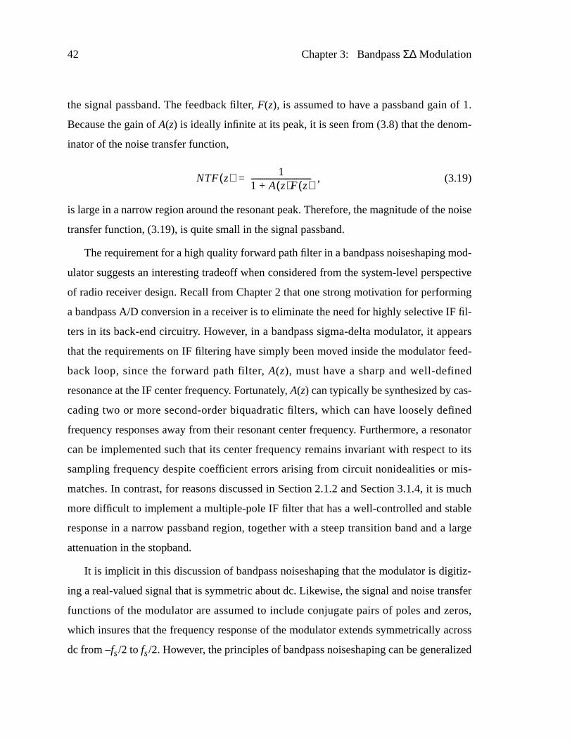
42 Chapter 3: BandpassΣ∆ Modulation
the signal passband. The feedback filter, F(z), is assumed to have a passband gain of 1.
Because the gain ofA(z) is ideally infinite at its peak, it is seen from (3.8) that the denom-
inator of the noise transfer function,
, (3.19)
is large in a narrow region around the resonant peak. Therefore, the magnitude of the noise
transfer function, (3.19), is quite small in the signal passband.
The requirement for a high quality forward path filter in a bandpass noiseshaping mod-
ulator suggests an interesting tradeoff when considered from the system-level perspective
of radio receiver design. Recall from Chapter 2 that one strong motivation for performing
a bandpass A/D conversion in a receiver is to eliminate the need for highly selective IF fil-
ters in its back-end circuitry. However, in a bandpass sigma-delta modulator, it appears
that the requirements on IF filtering have simply been moved inside the modulator feed-
back loop, since the forward path filter, A(z), must have a sharp and well-defined
resonance at the IF center frequency. Fortunately, A(z) can typically be synthesized by cas-
cading two or more second-order biquadratic filters, which can have loosely defined
frequency responses away from their resonant center frequency. Furthermore, a resonator
can be implemented such that its center frequency remains invariant with respect to its
sampling frequency despite coefficient errors arising from circuit nonidealities or mis-
matches. In contrast, for reasons discussed in Section2.1.2 and Section3.1.4, it is much
more difficult to implement a multiple-pole IF filter that has a well-controlled and stable
response in a narrow passband region, together with a steep transition band and a large
attenuation in the stopband.
It is implicit in this discussion of bandpass noiseshaping that the modulator is digitiz-
ing a real-valued signal that is symmetric about dc. Likewise, the signal and noise transfer
functions of the modulator are assumed to include conjugate pairs of poles and zeros,
which insures that the frequency response of the modulator extends symmetrically across
dc from –fs/2 to fs/2. However, the principles of bandpass noiseshaping can be generalized
NTF z( ) 11 A z( )F z( )+--------------------------------=
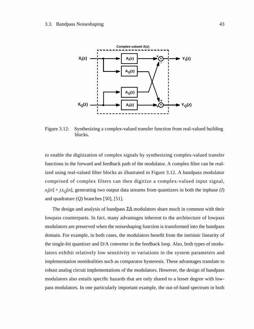
3.3. Bandpass Noiseshaping 43
to enable the digitization of complex signals by synthesizing complex-valued transfer
functions in the forward and feedback path of the modulator. A complex filter can be real-
ized using real-valued filter blocks as illustrated in Figure3.12. A bandpass modulator
comprised of complex filters can then digitize a complex-valued input signal,
xI[n] + j xQ[n], generating two output data streams from quantizers in both the inphase (I)
and quadrature (Q) branches [50], [51].
The design and analysis of bandpassΣ∆ modulators share much in common with their
lowpass counterparts. In fact, many advantages inherent to the architecture of lowpass
modulators are preserved when the noiseshaping function is transformed into the bandpass
domain. For example, in both cases, the modulators benefit from the intrinsic linearity of
the single-bit quantizer and D/A converter in the feedback loop. Also, both types of modu-
lators exhibit relatively low sensitivity to variations in the system parameters and
implementation nonidealities such as comparator hysteresis. These advantages translate to
robust analog circuit implementations of the modulators. However, the design of bandpass
modulators also entails specific hazards that are only shared to a lesser degree with low-
pass modulators. In one particularly important example, the out-of-band spectrum in both
Figure3.12: Synthesizing a complex-valued transfer function from real-valued buildingblocks.
++
XI(z) AI(z)
AQ(z)
AQ(z)
AI(z)
++
–
+XQ(z)
YI(z)
YQ(z)
Complex-valued A(z)
44 Chapter 3: BandpassΣ∆ Modulation
lowpass and bandpass modulators is contaminated by the presence of strong spectral
tones. In lowpass modulators, high-level tones have been reported nearfs/2 [52], [53],
which are easily rejected by the digital lowpass filter that follows the modulator. However,
in bandpass modulators, strong tones have been reported near dc as well asfs/2 [54].
Although these tones also lie in the stopband region, they can potentially degrade the noise
and distortion characteristics of the bandpass modulator by mixing with the input signal
and falling into the passband. This hazard can be partially defused by centering the signal
passband away fromfs/4, but the architecture of the modulator then becomes considerably
more complicated, and it may be difficult to guarantee the stability of the modulator. The
remainder of this section is devoted to a discussion of these hazards and other design
issues relevant to modulators that center the noise suppression region at an intermediate
frequency between dc andfs/2.
3.3.1 Passband Location
The passband of a bandpass modulator can be situated anywhere in the sampling band-
width from –fs/2 to fs/2. However, there are several compelling advantages gained by
forcing the passband to lie exactly at one-quarter of the sampling frequency. First, compar-
atively simple analog circuits can be used to implement the modulator, which may be a
necessity if the modulator is to operate at high sampling frequencies. Second, one class of
fs/4 bandpass topologies can easily be derived from lowpass prototypes with a simple
mathematical transformation to be described in Section3.3.2. Finally, as discussed in
Section2.3,I andQ demodulation is especially straightforward when the passband is cen-
tered atfs/4. The tradeoff for this architectural choice is that the dynamic range of the
modulator becomes increasingly constrained by circuit nonidealities at the high sampling
rates needed to digitize signals at IF locations above 10MHz. A detailed discussion of the
analog circuits comprising the modulator is delayed until Chapter 6.
The choice of passband may also be influenced by the requirements imposed on the
antialiasing filter that precedes the modulator. Figure3.13 illustrates how the transition
band of the filter becomes sharper as the passband moves away from dc. In order to avoid
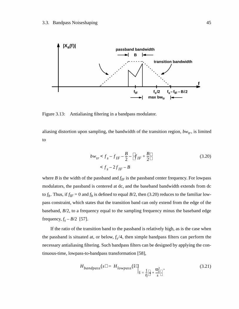
3.3. Bandpass Noiseshaping 45
aliasing distortion upon sampling, the bandwidth of the transition region, bwtr , is limited
to
(3.20)
whereB is the width of the passband andfIF is the passband center frequency. For lowpass
modulators, the passband is centered at dc, and the baseband bandwidth extends from dc
to fb. Thus, iffIF = 0 andfb is defined to equalB/2, then (3.20) reduces to the familiar low-
pass constraint, which states that the transition band can only extend from the edge of the
baseband,B/2, to a frequency equal to the sampling frequency minus the baseband edge
frequency, fs – B/2 [57].
If the ratio of the transition band to the passband is relatively high, as is the case when
the passband is situated at, or below, fs/4, then simple bandpass filters can perform the
necessary antialiasing filtering. Such bandpass filters can be designed by applying the con-
tinuous-time, lowpass-to-bandpass transformation [58],
(3.21)
Figure3.13: Antialiasing filtering in a bandpass modulator.
f
|Xa(f )|
fIF
B
fs /2 fs – fIF – B /2
transition bandwidth
max bw tr
passband bandwidth
f s 2 f IF– B–<
bwtr f s f IF– B2---– f IF
B2---+
–<
Hbandpass s( ) H lowpass s( )s
1η--- s
ωo2
s-------+
=
= ,
46 Chapter 3: BandpassΣ∆ Modulation
to a lowpass prototype filter. In (3.21),ωo is the center frequency of the bandpass filter,
andη is a scaling factor that affects the width of the passband. The passband edges of the
new bandpass filter are
(3.22)
whereωlp is the edge of the passband in the prototype lowpass filter. As the passband cen-
ter frequency approachesfs/2, the allowable transition region bandwidth diminishes
according to (3.20), with the cutoff requirements for the antialiasing filter eventually
approaching those imposed on the bandlimiting filter that precedes Nyquist-rate
converters.
3.3.2 Transformation fr om dc tofs/4
One class of bandpass modulators that centers the passband atfs/4 can be easily derived
by applying the mathematical transformation
(3.23)
to theLth-order, noise-differencing lowpass architecture depicted in Figure3.11 [55], [56].
This dc-to-fs/4 transformation effectively replaces the integrators in anLth-order, lowpass
prototype with two-pole, bandpass resonators that ideally realize an infinite gain atfs/4. If
(3.23) is applied to a delaying, discrete-time integrator, then the resulting bandpass resona-
tor has the transfer function
. (3.24)
In the same manner, if the second-order, lowpass modulator of Figure3.9 is transformed
to the bandpass domain via (3.23), the canonical, fourth-order, fs/4 bandpass modulator
depicted in Figure3.14 results. This topology is referred to as being canonical because it
is derived directly from the original, second-order topology described by Candy for low-
ωbp1 ωbp2,ωlpη
2------------ ωo
2ωlpη
2------------
2
++±=
z 1– z 2––→
Hbp z( ) z 1–
1 z 1––----------------
z 1– z 2––=
z 2––
1 z 2–+-----------------= =
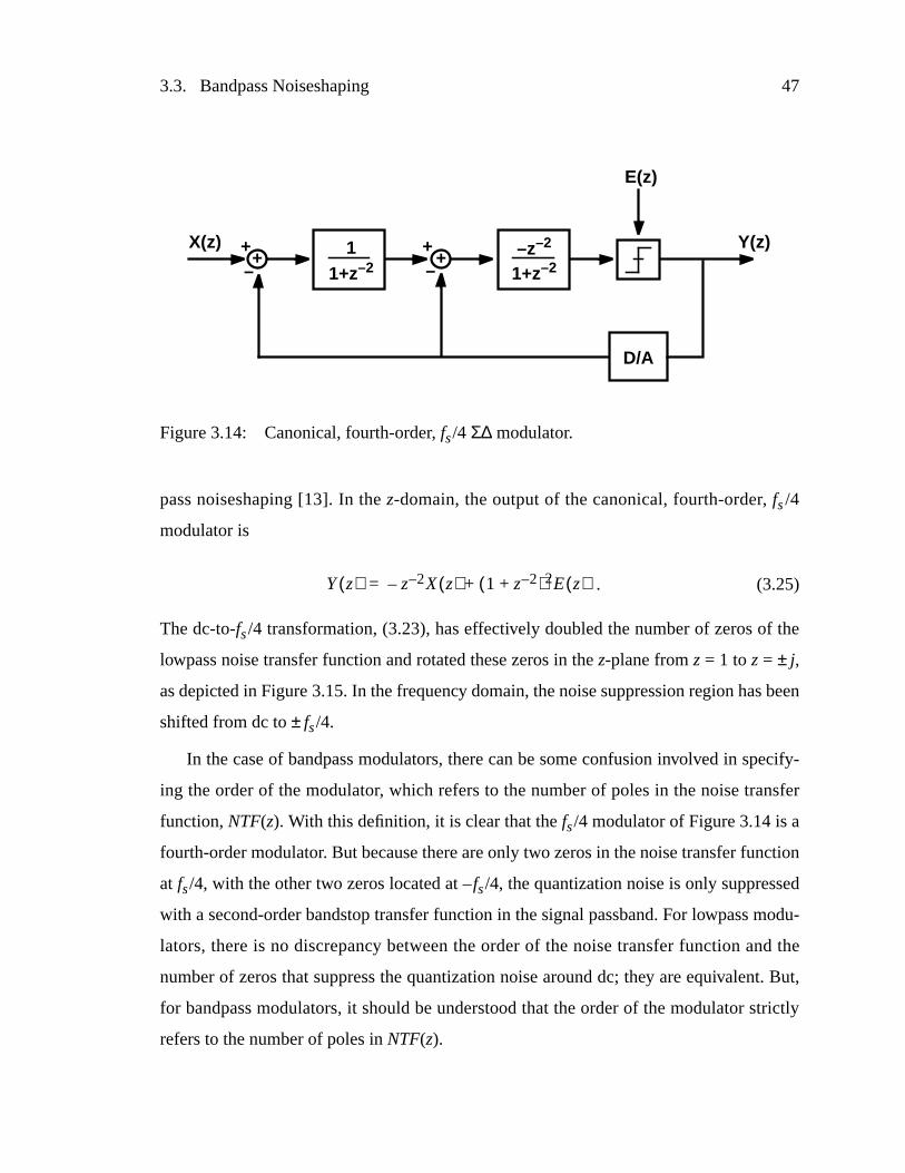
3.3. Bandpass Noiseshaping 47
pass noiseshaping [13]. In thez-domain, the output of the canonical, fourth-order, fs/4
modulator is
. (3.25)
The dc-to-fs/4 transformation, (3.23), has effectively doubled the number of zeros of the
lowpass noise transfer function and rotated these zeros in thez-plane fromz = 1 toz = ± j,
as depicted in Figure3.15. In the frequency domain, the noise suppression region has been
shifted from dc to± fs/4.
In the case of bandpass modulators, there can be some confusion involved in specify-
ing the order of the modulator, which refers to the number of poles in the noise transfer
function,NTF(z). With this definition, it is clear that thefs/4 modulator of Figure3.14 is a
fourth-order modulator. But because there are only two zeros in the noise transfer function
at fs/4, with the other two zeros located at –fs/4, the quantization noise is only suppressed
with a second-order bandstop transfer function in the signal passband. For lowpass modu-
lators, there is no discrepancy between the order of the noise transfer function and the
number of zeros that suppress the quantization noise around dc; they are equivalent. But,
for bandpass modulators, it should be understood that the order of the modulator strictly
refers to the number of poles inNTF(z).
Figure3.14: Canonical, fourth-order, fs/4 Σ∆ modulator.
+X(z) Y(z)+
–
D/A
E(z)
11+z–2 +
+–
–z–2
1+z–2
Y z( ) z 2– X z( )– 1 z 2–+( )2E z( )+=
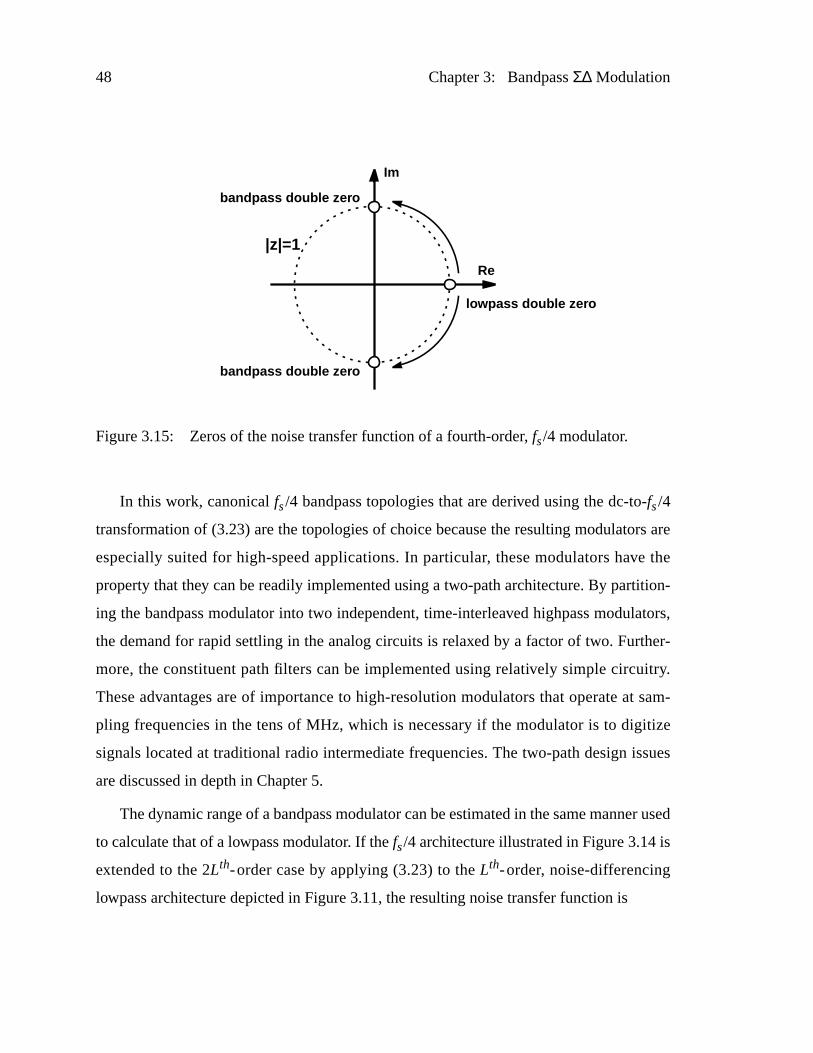
48 Chapter 3: BandpassΣ∆ Modulation
In this work, canonicalfs/4 bandpass topologies that are derived using the dc-to-fs/4
transformation of (3.23) are the topologies of choice because the resulting modulators are
especially suited for high-speed applications. In particular, these modulators have the
property that they can be readily implemented using a two-path architecture. By partition-
ing the bandpass modulator into two independent, time-interleaved highpass modulators,
the demand for rapid settling in the analog circuits is relaxed by a factor of two. Further-
more, the constituent path filters can be implemented using relatively simple circuitry.
These advantages are of importance to high-resolution modulators that operate at sam-
pling frequencies in the tens of MHz, which is necessary if the modulator is to digitize
signals located at traditional radio intermediate frequencies. The two-path design issues
are discussed in depth in Chapter 5.
The dynamic range of a bandpass modulator can be estimated in the same manner used
to calculate that of a lowpass modulator. If the fs/4 architecture illustrated in Figure3.14 is
extended to the 2Lth-order case by applying (3.23) to theLth-order, noise-differencing
lowpass architecture depicted in Figure3.11, the resulting noise transfer function is
Figure3.15: Zeros of the noise transfer function of a fourth-order, fs/4 modulator.
bandpass doub le zero
bandpass doub le zero
lowpass doub le zero
Re
Im
|z|=1
3.3. Bandpass Noiseshaping 49
, (3.26)
which in the frequency domain, can be written as
. (3.27)
Assuming that the quantization noise,E(z), is additive, with a total power of∆2/12 that is
distributed uniformly in the sampling bandwidth, –fs/2 to fs/2, the power spectral density
of E(z) is
. (3.28)
The quantization noise is shaped by the transfer function
. (3.29)
The power of the quantization noise in the passband can be found by integrating the power
spectral density of the shaped quantization noise,
, (3.30)
over the signal bandwidth centered atfs/4. The out-of-band quantization noise is assumed
to be rejected by a digital filter that follows the modulator. SinceB << fs, the integral can
be evaluated under the approximation sin(x) ≈ x to yield an inband quantization noise
power equal to
NTF z( ) 1 z 2–+( )L=
NTF f( ) NTF z( )z e
j2πf Ts=1 e
j– 4πf Ts+( )L= =
Se f( ) ∆2
12------ 1
f s----- ,×=
f s
2----- f
f s
2-----< <–
NTFe f( ) 2 2 2πf Tscos( )2L=
SQ f( ) 2 2πf Tscos( )2L ∆2
12------ 1
f s-----× ,⋅=
f s
2----- f
f s
2-----< <–
50 Chapter 3: BandpassΣ∆ Modulation
(3.31)
whereM is defined asfs/(2 × B), with B being the width of the signal passband, as illus-
trated in Figure3.13.
In cases where the signal passband is centered at an intermediate frequency, it is not
strictly correct to refer toM as the oversampling ratio. The oversampling ratio is defined
as the ratio of the actual sampling frequency to the minimum sampling frequency that
avoids destructive aliasing. For lowpass modulators, the signal bandwidth extends from dc
to fb; thus, the minimum sampling frequency that avoids destructive aliasing is 2× fb,
which is commonly referred to as the Nyquist rate. Therefore, the oversampling ratio for a
lowpass modulator is equal to the sampling frequency divided by the Nyquist rate,
fs/(2 × fb). However, for bandpass signals, in which the signal passband has a bandwidth
of B and is centered at an intermediate frequency, fIF, the minimum sampling frequency
required to avoid destructive aliasing is only approximately equal to 2× B. The exact
expression for the minimum sampling frequency is
(3.32)
PQ SQ f( ) fd
f s
4-----– B
2---–
f s
4-----– B
2---+
∫ SQ f( ) fd
f s
4----- B
2---–
f s
4----- B
2---+
∫+=
2 2 2πf Tscos( )2L ∆2
12------ 1
f s-----⋅ ⋅ fd
f s
4----- B
2---–
f s
4----- B
2---+
∫×=
∆2
12------≈ π2L
2L 1+----------------× 1
M2L 1+-------------------×
f min
2 f IFB2---+
f IFB2---+
B-------------------
---------------------------=
3.3. Bandpass Noiseshaping 51
where x is equal to the largest integer not exceedingx [59], [60]. Hence, the oversam-
pling ratio in a bandpass system should be defined asfs/fmin with fmin given by (3.32).
Regardless, the convention in the literature for bandpass modulators is to refer to
fs/ (2 × B) as the oversampling ratio in order to preserve the terminology from lowpass
modulators. Thus, the expression for the inband noise power calculated in (3.31) takes on
the same form as the expression derived for anLth-order lowpass modulator, (3.17). The
expression for the dynamic range of the canonical 2Lth-order, fs/4 modulator,
, (3.33)
also corresponds to that of anLth-order lowpass modulator, (3.18).
The expressions that have been derived for the inband noise power, (3.31), and
dynamic range, (3.33), of a 2Lth-order, fs/4 modulator closely match the results of behav-
ioral simulations of the modulator using MIDAS [61]. The following figures show results
from these simulations. In the following discussion, the modulator’s full-scale analog
input range is defined as the step size of its single-bit quantizer, ∆. Thus, the 0 dB level
corresponds to the power of a sinusoid with an amplitude of∆ /2. Figure3.16 shows the
undecimated spectrum of the fourth-order, fs/4 modulator of Figure3.14 when a –10 dB
input been applied. In Figure3.17, the signal-to-noise ratio in a 200-kHz passband vs.
input signal level is seen to closely correspond to the straight-line characteristic derived
from a linearized model of the modulator. However, it is not evident from these figures
that large families of out-of-band tones begin to emerge at dc andfs/2 when the input sig-
nal level decreases below approximately –40 dB. An example of these tones is illustrated
in Figure3.18 for a –50 dB input signal. Under normal modulator operation, the existence
of such tones would not be problematic because they are ostensibly rejected by the digital
decimation filter. However, if distortion mechanisms are present in the analog implemen-
tation of the modulator, then out-of-band tones at dc andfs/4 can mix with the input signal
and fall into the passband centered atfs/4. In Chapter 7, it is postulated that this type of
DR
12--- ∆
2---
2
∆2
12------ π2L
2L 1+----------------× 1
M2L 1+-------------------×
-------------------------------------------------------32--- M2L 1+× 2L 1+
π2L----------------×= =
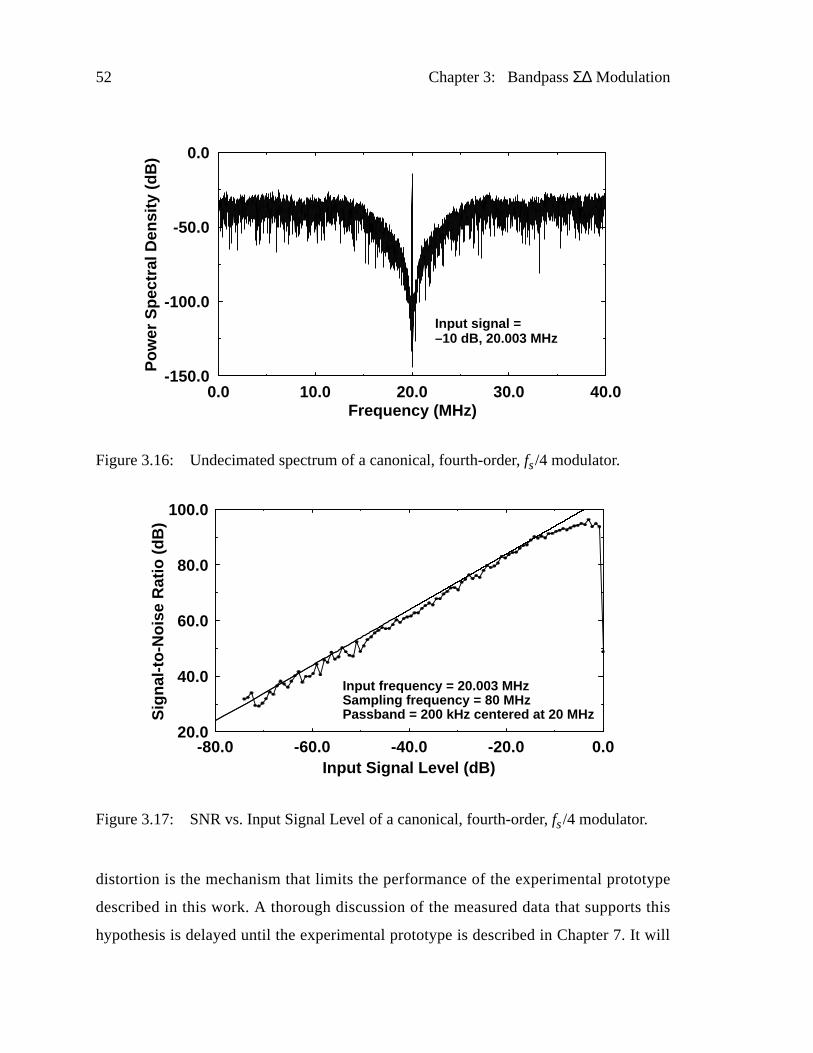
52 Chapter 3: BandpassΣ∆ Modulation
distortion is the mechanism that limits the performance of the experimental prototype
described in this work. A thorough discussion of the measured data that supports this
hypothesis is delayed until the experimental prototype is described in Chapter 7. It will
Figure3.16: Undecimated spectrum of a canonical, fourth-order, fs/4 modulator.
0.0 10.0 20.0 30.0 40.0-150.0
-100.0
-50.0
0.0
Frequency (MHz)
Pow
er S
pect
ral D
ensi
ty (
dB)
Input signal =–10 dB, 20.003 MHz
Figure3.17: SNR vs. Input Signal Level of a canonical, fourth-order, fs/4 modulator.
Input Signal Level (dB)
Sig
nal-t
o-N
oise
Rat
io (
dB)
-80.0 -60.0 -40.0 -20.0 0.020.0
40.0
60.0
80.0
100.0
Input frequency = 20.003 MHzSampling frequency = 80 MHzPassband = 200 kHz centered at 20 MHz
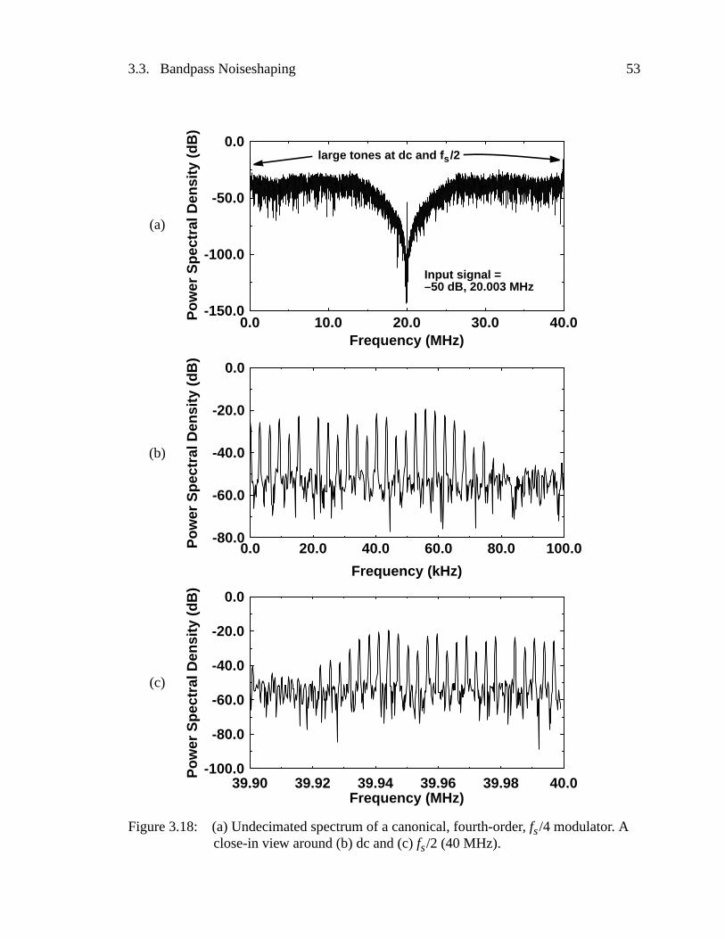
3.3. Bandpass Noiseshaping 53
Figure3.18: (a) Undecimated spectrum of a canonical, fourth-order, fs/4 modulator. Aclose-in view around (b) dc and (c)fs/2 (40 MHz).
0.0 10.0 20.0 30.0 40.0-150.0
-100.0
-50.0
0.0
0.0 20.0 40.0 60.0 80.0 100.0-80.0
-60.0
-40.0
-20.0
0.0
Frequency (MHz)
39.90 39.92 39.94 39.96 39.98 40.0-100.0
-80.0
-60.0
-40.0
-20.0
0.0
Frequency (kHz)
Frequency (MHz)
(a)
(c)
(b)
Pow
er S
pect
ral D
ensi
ty (
dB)
Pow
er S
pect
ral D
ensi
ty (
dB)
Pow
er S
pect
ral D
ensi
ty (
dB)
Input signal =–50 dB, 20.003 MHz
large tones at dc and f s /2
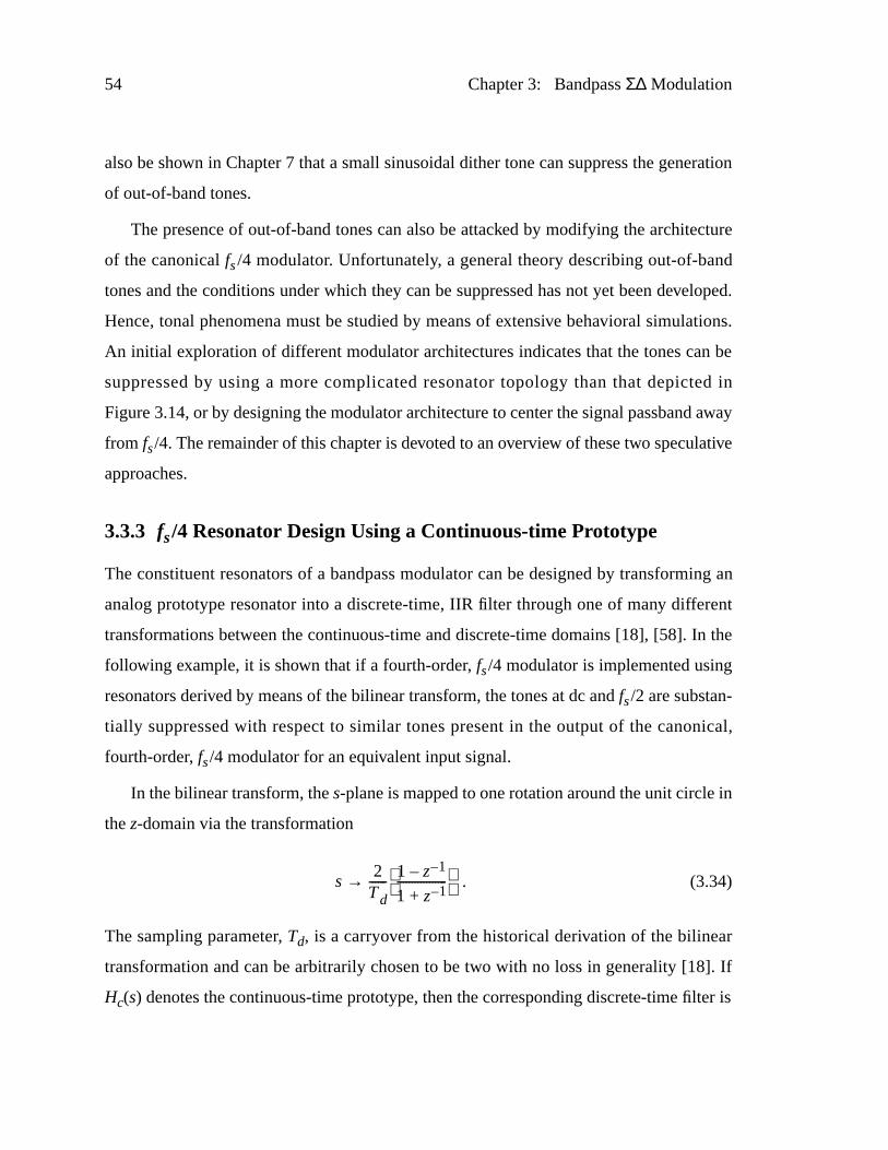
54 Chapter 3: BandpassΣ∆ Modulation
also be shown in Chapter 7 that a small sinusoidal dither tone can suppress the generation
of out-of-band tones.
The presence of out-of-band tones can also be attacked by modifying the architecture
of the canonicalfs/4 modulator. Unfortunately, a general theory describing out-of-band
tones and the conditions under which they can be suppressed has not yet been developed.
Hence, tonal phenomena must be studied by means of extensive behavioral simulations.
An initial exploration of different modulator architectures indicates that the tones can be
suppressed by using a more complicated resonator topology than that depicted in
Figure3.14, or by designing the modulator architecture to center the signal passband away
from fs/4. The remainder of this chapter is devoted to an overview of these two speculative
approaches.
3.3.3 fs/4 Resonator Design Using a Continuous-time Prototype
The constituent resonators of a bandpass modulator can be designed by transforming an
analog prototype resonator into a discrete-time, IIR filter through one of many different
transformations between the continuous-time and discrete-time domains [18], [58]. In the
following example, it is shown that if a fourth-order, fs/4 modulator is implemented using
resonators derived by means of the bilinear transform, the tones at dc andfs/2 are substan-
tially suppressed with respect to similar tones present in the output of the canonical,
fourth-order, fs/4 modulator for an equivalent input signal.
In the bilinear transform, thes-plane is mapped to one rotation around the unit circle in
thez-domain via the transformation
. (3.34)
The sampling parameter, Td, is a carryover from the historical derivation of the bilinear
transformation and can be arbitrarily chosen to be two with no loss in generality [18]. If
Hc(s) denotes the continuous-time prototype, then the corresponding discrete-time filter is
s2
Td------ 1 z 1––
1 z 1–+-----------------
→
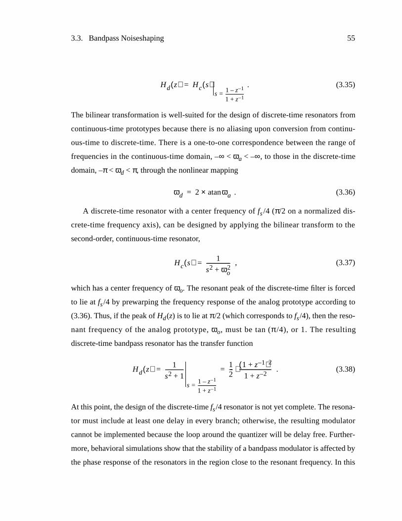
3.3. Bandpass Noiseshaping 55
. (3.35)
The bilinear transformation is well-suited for the design of discrete-time resonators from
continuous-time prototypes because there is no aliasing upon conversion from continu-
ous-time to discrete-time. There is a one-to-one correspondence between the range of
frequencies in the continuous-time domain, –∞ < ωa < –∞, to those in the discrete-time
domain, –π< ωd < π, through the nonlinear mapping
. (3.36)
A discrete-time resonator with a center frequency of fs/4 (π/2 on a normalized dis-
crete-time frequency axis), can be designed by applying the bilinear transform to the
second-order, continuous-time resonator,
, (3.37)
which has a center frequency of ωo. The resonant peak of the discrete-time filter is forced
to lie atfs/4 by prewarping the frequency response of the analog prototype according to
(3.36). Thus, if the peak ofHd(z) is to lie atπ/2 (which corresponds tofs/4), then the reso-
nant frequency of the analog prototype,ωo, must be tan(π/4), or 1. The resulting
discrete-time bandpass resonator has the transfer function
. (3.38)
At this point, the design of the discrete-timefs/4 resonator is not yet complete. The resona-
tor must include at least one delay in every branch; otherwise, the resulting modulator
cannot be implemented because the loop around the quantizer will be delay free. Further-
more, behavioral simulations show that the stability of a bandpass modulator is affected by
the phase response of the resonators in the region close to the resonant frequency. In this
Hd z( ) Hc s( )s
1 z 1––1 z 1–+-----------------=
=
ωd 2 ωaatan×=
Hc s( ) 1
s2 ωo2+
------------------=
Hd z( ) 1
s2 1+--------------
s1 z 1––1 z 1–+-----------------=
12--- 1 z 1–+( )2
1 z 2–+------------------------⋅= =
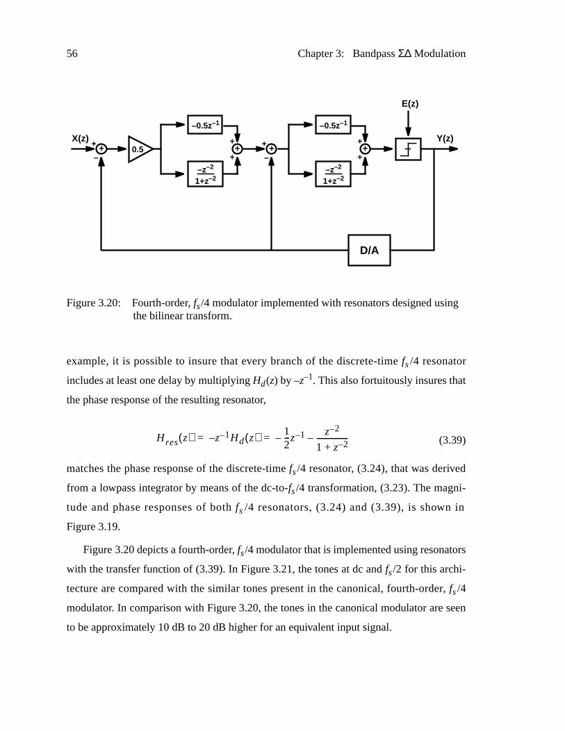
56 Chapter 3: BandpassΣ∆ Modulation
example, it is possible to insure that every branch of the discrete-timefs/4 resonator
includes at least one delay by multiplyingHd(z) by –z–1. This also fortuitously insures that
the phase response of the resulting resonator,
(3.39)
matches the phase response of the discrete-timefs/4 resonator, (3.24), that was derived
from a lowpass integrator by means of the dc-to-fs/4 transformation, (3.23). The magni-
tude and phase responses of bothfs /4 resonators, (3.24) and (3.39), is shown in
Figure3.19.
Figure3.20 depicts a fourth-order, fs/4 modulator that is implemented using resonators
with the transfer function of (3.39). In Figure3.21, the tones at dc andfs/2 for this archi-
tecture are compared with the similar tones present in the canonical, fourth-order, fs/4
modulator. In comparison with Figure3.20, the tones in the canonical modulator are seen
to be approximately 10 dB to 20dB higher for an equivalent input signal.
Hres z( ) z 1– H– d z( ) 12---z 1–– z 2–
1 z 2–+-----------------–= =
Figure3.20: Fourth-order, fs/4 modulator implemented with resonators designed usingthe bilinear transform.
+0.5X(z) Y(z)
–z–2
1+z–2
–0.5z–1
+ +
–0.5z–1
E(z)
+
–z–2
1+z–2
D/A
+
–
+
–
+
+
+
+
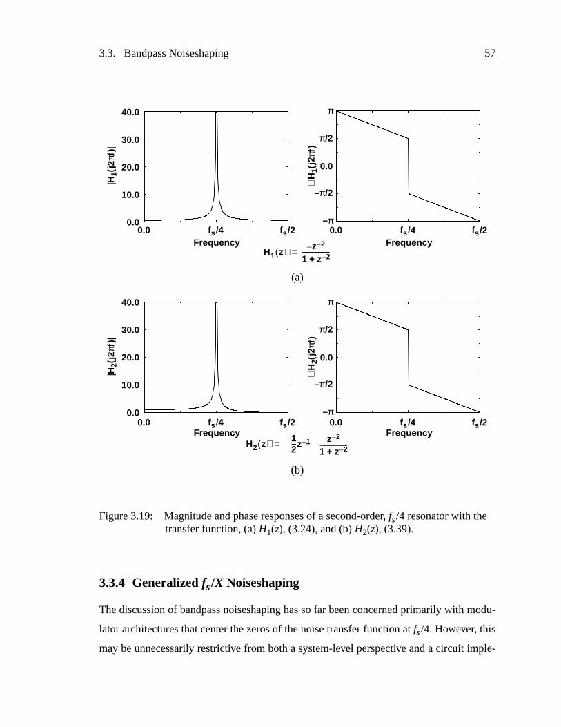
3.3. Bandpass Noiseshaping 57
3.3.4 Generalizedfs/X Noiseshaping
The discussion of bandpass noiseshaping has so far been concerned primarily with modu-
lator architectures that center the zeros of the noise transfer function atfs/4. However, this
may be unnecessarily restrictive from both a system-level perspective and a circuit imple-
Figure3.19: Magnitude and phase responses of a second-order, fs/4 resonator with thetransfer function, (a)H1(z), (3.24), and (b)H2(z), (3.39).
0.0
20.0
40.0
0.0 fs /4 fs /2
0.0
10.0
20.0
30.0
40.0
π
π/2
0.0
–π/2
–π
10.0
30.0
0.0 fs /4 fs /2
0.0 fs /4 fs /2
π
π/2
0.0
–π/2
–π0.0 fs /4 fs /2
Frequency
|H1(
j2πf
)|
∠H
1(j2
πf)
Frequency
Frequency
|H2(
j2πf
)|
∠H
2(j2
πf)
Frequency
H1 z( ) z 2––1 z 2–+------------------=
H2 z( ) 12---z 1–– z 2–
1 z 2–+------------------–=
(a)
(b)
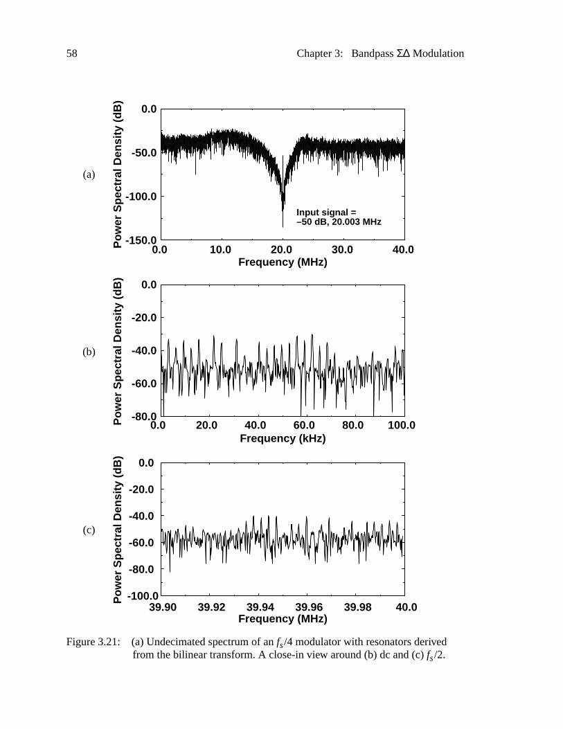
58 Chapter 3: BandpassΣ∆ Modulation
Figure3.21: (a) Undecimated spectrum of anfs/4 modulator with resonators derivedfrom the bilinear transform. A close-in view around (b) dc and (c)fs/2.
0.0 10.0 20.0 30.0 40.0-150.0
-100.0
-50.0
0.0
0.0 20.0 40.0 60.0 80.0 100.0-80.0
-60.0
-40.0
-20.0
0.0
39.90 39.92 39.94 39.96 39.98 40.0-100.0
-80.0
-60.0
-40.0
-20.0
0.0
Frequency (MHz)
Frequency (kHz)
Frequency (MHz)
Input signal =–50 dB, 20.003 MHz
Pow
er S
pect
ral D
ensi
ty (
dB)
Pow
er S
pect
ral D
ensi
ty (
dB)
Pow
er S
pect
ral D
ensi
ty (
dB)
(a)
(c)
(b)
3.3. Bandpass Noiseshaping 59
mentation standpoint. Two primary considerations motivate relocating the signal passband
to a generalized location atfs/X, where 2 <X < ∞. First, when the passband is centered
away fromfs/4, any distortion products resulting from the mixing of tones atfs/2 with the
input signal will fall outside the passband. Therefore, concern over out-of-band tones is
partially relieved. Second, if the passband center frequency is situated betweenfs/4 and
fs/2, the ratio of the modulator’s sampling frequency to its passband center frequency is
reduced. Therefore, if the modulator is implemented with a single-path topology, the
demands upon the analog circuitry will be relaxed when the sampling rate is reduced.
However, it should be noted that once the passband is centered away fromfs/4, the result-
ing modulator may not be suitable for implementation using the type of two-path
architecture that is advantageous for modulators operating at high sampling speeds. This
two-path architecture is developed in detail in Chapters 4 and 5.
The zeros of the noise transfer function can be positioned anywhere between dc and
fs/2 by generalizing the dc-to-fs/4 transformation, (3.23), to allow the constituent resona-
tors to realize their nominally infinite gain in a passband that is centered at any arbitrary
frequency, fs/X. If this transformation process yields a modulator architecture with unde-
sirable characteristics, such as poor stability or overload recovery, then an alternative
direct synthesis method may be employed. In this approach, the architecture of the band-
pass modulator is designed to implement the desired noiseshaping function without
relying on a transformation from the lowpass domain. The remainder of this chapter is
devoted to a discussion of these two design procedures. It should be emphasized that the
methodologies to be presented are neither complete nor proven to be optimal. In fact, in
the absence of definitive theoretical analyses, extensive behavioral simulations of modula-
tor architectures and empirical evidence in the open literature are offered as the only
justification for the guidelines stated.
3.3.4.1 Constantinides Lowpass-to-Bandpass Transformation
Intuitively, if the integrators of theLth-order, lowpass modulator depicted in Figure3.11
are replaced by resonators that peak atfs/X, then quantization noise will be suppressed in a
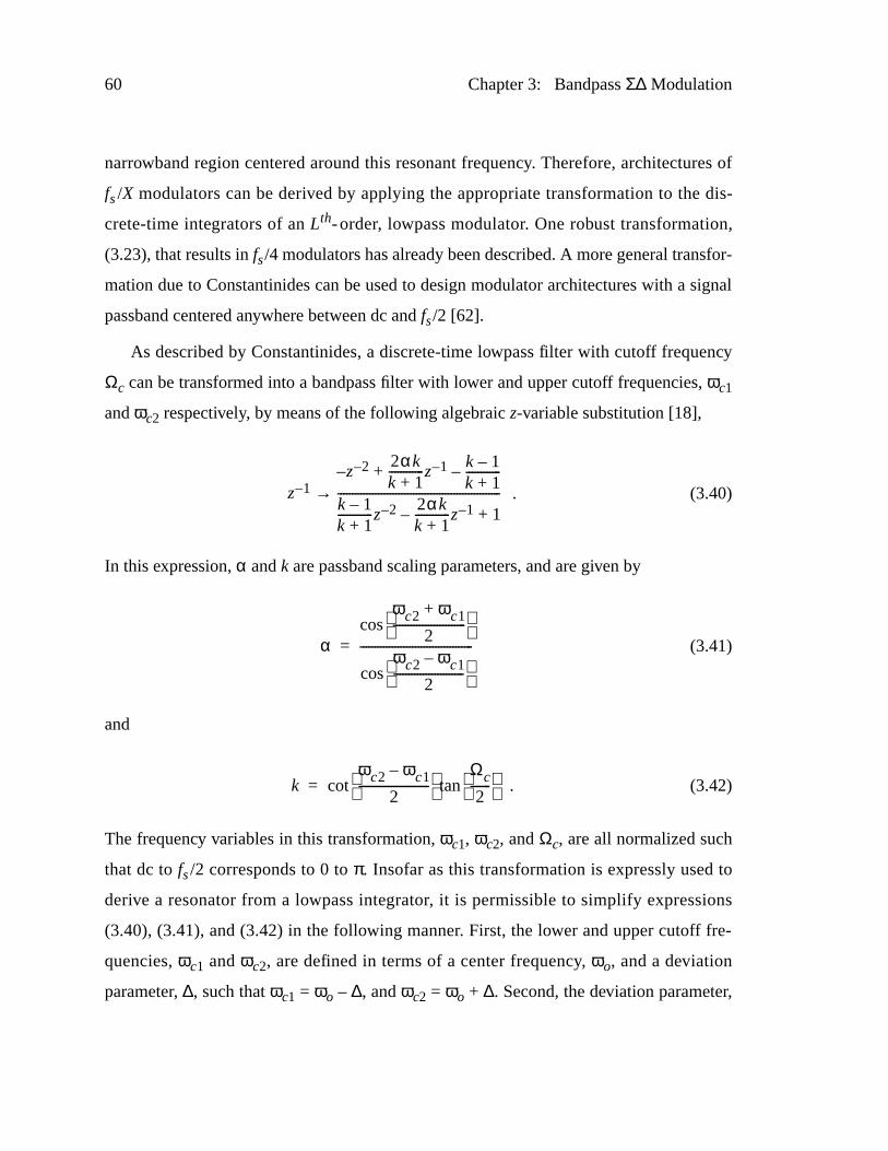
60 Chapter 3: BandpassΣ∆ Modulation
narrowband region centered around this resonant frequency. Therefore, architectures of
fs/X modulators can be derived by applying the appropriate transformation to the dis-
crete-time integrators of anLth-order, lowpass modulator. One robust transformation,
(3.23), that results infs/4 modulators has already been described. A more general transfor-
mation due to Constantinides can be used to design modulator architectures with a signal
passband centered anywhere between dc andfs/2 [62].
As described by Constantinides, a discrete-time lowpass filter with cutoff frequency
Ωc can be transformed into a bandpass filter with lower and upper cutoff frequencies,ωc1
andωc2 respectively, by means of the following algebraicz-variable substitution [18],
. (3.40)
In this expression,α andk are passband scaling parameters, and are given by
(3.41)
and
. (3.42)
The frequency variables in this transformation,ωc1, ωc2, andΩc, are all normalized such
that dc tofs/2 corresponds to 0 toπ. Insofar as this transformation is expressly used to
derive a resonator from a lowpass integrator, it is permissible to simplify expressions
(3.40), (3.41), and (3.42) in the following manner. First, the lower and upper cutoff fre-
quencies,ωc1 andωc2, are defined in terms of a center frequency, ωo, and a deviation
parameter, ∆, such thatωc1 = ωo – ∆, andωc2 = ωo + ∆. Second, the deviation parameter,
z 1–z– 2– 2αk
k 1+------------z 1– k 1–
k 1+------------–+
k 1–k 1+------------z 2– 2αk
k 1+------------z 1–– 1+
--------------------------------------------------------→
α
ωc2 ωc1+
2-------------------------
cos
ωc2 ωc1–
2------------------------
cos
---------------------------------------=
kωc2 ωc1–
2------------------------
cotΩc
2-------
tan=
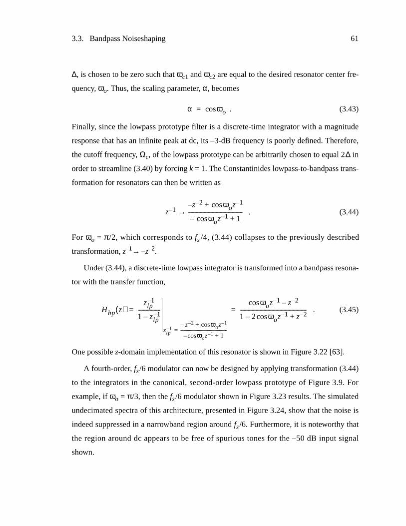
3.3. Bandpass Noiseshaping 61
∆, is chosen to be zero such thatωc1 andωc2 are equal to the desired resonator center fre-
quency, ωo. Thus, the scaling parameter, α, becomes
. (3.43)
Finally, since the lowpass prototype filter is a discrete-time integrator with a magnitude
response that has an infinite peak at dc, its –3-dB frequency is poorly defined. Therefore,
the cutoff frequency, Ωc, of the lowpass prototype can be arbitrarily chosen to equal 2∆ in
order to streamline (3.40) by forcingk = 1. The Constantinides lowpass-to-bandpass trans-
formation for resonators can then be written as
. (3.44)
For ωo = π/2, which corresponds tofs/4, (3.44) collapses to the previously described
transformation,z–1→ –z–2.
Under (3.44), a discrete-time lowpass integrator is transformed into a bandpass resona-
tor with the transfer function,
. (3.45)
One possiblez-domain implementation of this resonator is shown in Figure3.22 [63].
A fourth-order, fs/6 modulator can now be designed by applying transformation (3.44)
to the integrators in the canonical, second-order lowpass prototype of Figure3.9. For
example, ifωo = π/3, then thefs/6 modulator shown in Figure3.23 results. The simulated
undecimated spectra of this architecture, presented in Figure3.24, show that the noise is
indeed suppressed in a narrowband region aroundfs/6. Furthermore, it is noteworthy that
the region around dc appears to be free of spurious tones for the –50 dB input signal
shown.
α ωocos=
z 1–z– 2– ωocos z 1–+
ωocos z 1–– 1+-----------------------------------------→
Hbp z( )zlp
1–
1 zlp1––
-----------------
zl p1–
z 2–– ωoz 1–cos+
ωoz 1– 1+cos–------------------------------------------=
ωoz 1– z 2––cos
1 2 ωoz 1– z 2–+cos–--------------------------------------------------= =
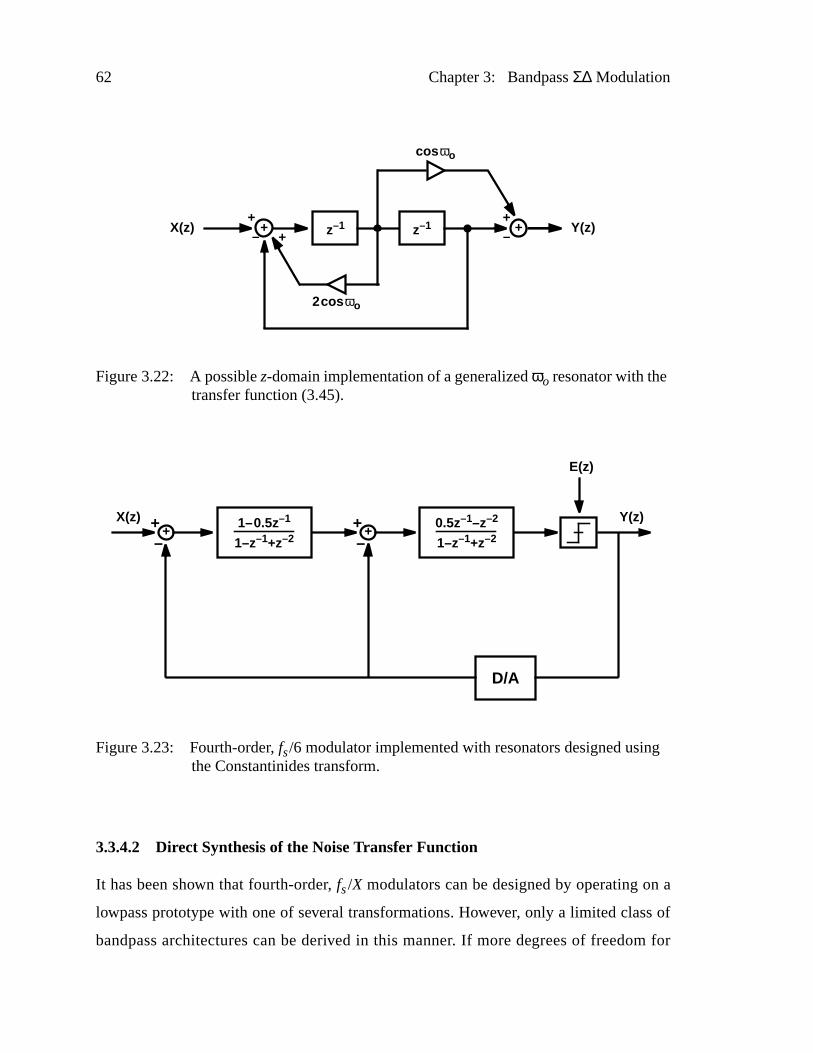
62 Chapter 3: BandpassΣ∆ Modulation
3.3.4.2 Dir ect Synthesis of the Noise Transfer Function
It has been shown that fourth-order, fs/X modulators can be designed by operating on a
lowpass prototype with one of several transformations. However, only a limited class of
bandpass architectures can be derived in this manner. If more degrees of freedom for
Figure3.22: A possiblez-domain implementation of a generalizedωo resonator with thetransfer function (3.45).
++– z–1 z–1
2cos ωo
cos ωo
++–
X(z) Y(z)+
Figure3.23: Fourth-order, fs/6 modulator implemented with resonators designed usingthe Constantinides transform.
X(z) Y(z)+
E(z)
+
D/A
+–
+–
1–0.5z–1
1–z–1+z–20.5z–1–z–2
1–z–1+z–2
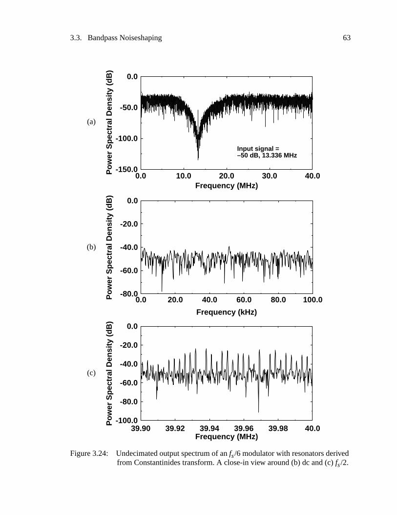
3.3. Bandpass Noiseshaping 63
Figure3.24: Undecimated output spectrum of anfs/6 modulator with resonators derivedfrom Constantinides transform. A close-in view around (b) dc and (c)fs/2.
0.0 10.0 20.0 30.0 40.0-150.0
-100.0
-50.0
0.0
0.0 20.0 40.0 60.0 80.0 100.0-80.0
-60.0
-40.0
-20.0
0.0
Frequency (MHz)
39.90 39.92 39.94 39.96 39.98 40.0-100.0
-80.0
-60.0
-40.0
-20.0
0.0
Frequency (kHz)
Frequency (MHz)
Pow
er S
pect
ral D
ensi
ty (
dB)
Pow
er S
pect
ral D
ensi
ty (
dB)
Pow
er S
pect
ral D
ensi
ty (
dB)
Input signal =–50 dB, 13.336 MHz
(a)
(c)
(b)
64 Chapter 3: BandpassΣ∆ Modulation
architectural optimization, or higher-order (2L > 4) noiseshaping in a single-loop topology
are desired, then the design process must be focused specifically on the noise transfer
function (NTF) of the modulator. From this perspective, the modulator design process is
essentially reduced to one of filter design; once a suitable NTF has been identified, an
architecture that implements this transfer function is synthesized.
Architectures derived by direct synthesis of the noise transfer function offer more flex-
ibility than those derived by transforming a lowpass prototype because the modulator can
be tuned with respect to specific performance metrics by manipulating the NTF. For exam-
ple, behavioral simulations show that the peak signal-to-quantization noise ratio near
overload is correlated with the out-of-band gain ofNTF(z). Therefore, if the peak SNR is
not sufficient, the NTF can be redesigned to have a larger out-of-band gain. This design
procedure opens the possibility of using computer-aided optimization tools to design an
NTF(z) that maximally suppresses the inband quantization noise with respect to a speci-
fied cost function [64]. In practice, however, this degree of optimization may not be
worthwhile because the minimum detectable signal in efficient implementations of modu-
lators is virtually always determined by circuit, rather than quantization, noise.
The direct synthesis of a bandpass noiseshaping modulator is similar in many ways to
the design of higher-order, single-loop, lowpass modulators, which are comprised of mul-
tiple (> 2) integrators embedded in a feedback topology. In both domains, lowpass as well
as bandpass, the design of the modulator begins with identifying a noise transfer function
that adheres to certain empirically derived criteria [45]-[47]. The concern is that the pres-
ence of multiple poles enclosed within a feedback loop will induce an instability in the
modulator. In this context, instability refers to the condition in which the internal states of
the modulator exhibit large, and possibly unbounded, excursions that persist even after the
input signal is removed. In addition, during overload or instability, the signal-to-noise ratio
at the output of the modulator will be substantially below that predicted by a linearized,
stochastic model of the system. The design goal is to inhibit this potential instability by
imposing restrictions on the shape and out-of-band gain of NTF(z), while insuring that
such constraints are not so severe as to compromise the inband noise suppression.
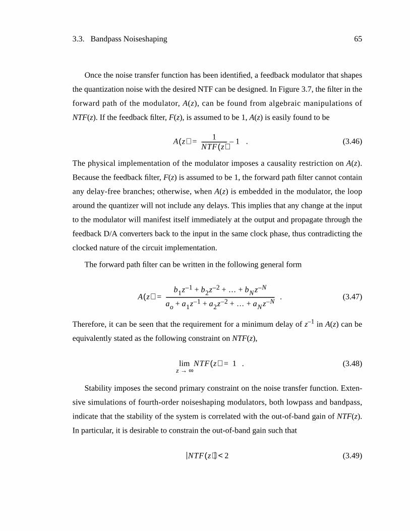
3.3. Bandpass Noiseshaping 65
Once the noise transfer function has been identified, a feedback modulator that shapes
the quantization noise with the desired NTF can be designed. In Figure3.7, the filter in the
forward path of the modulator, A(z), can be found from algebraic manipulations of
NTF(z). If the feedback filter, F(z), is assumed to be 1,A(z) is easily found to be
. (3.46)
The physical implementation of the modulator imposes a causality restriction onA(z).
Because the feedback filter, F(z) is assumed to be 1, the forward path filter cannot contain
any delay-free branches; otherwise, whenA(z) is embedded in the modulator, the loop
around the quantizer will not include any delays. This implies that any change at the input
to the modulator will manifest itself immediately at the output and propagate through the
feedback D/A converters back to the input in the same clock phase, thus contradicting the
clocked nature of the circuit implementation.
The forward path filter can be written in the following general form
. (3.47)
Therefore, it can be seen that the requirement for a minimum delay ofz–1 in A(z) can be
equivalently stated as the following constraint onNTF(z),
. (3.48)
Stability imposes the second primary constraint on the noise transfer function. Exten-
sive simulations of fourth-order noiseshaping modulators, both lowpass and bandpass,
indicate that the stability of the system is correlated with the out-of-band gain ofNTF(z).
In particular, it is desirable to constrain the out-of-band gain such that
(3.49)
A z( ) 1NTF z( )------------------- 1–=
A z( )b1z 1– b2z 2– … bNz N–+ + +
ao a1z 1– a2z 2– … aNz N–+ + + +---------------------------------------------------------------------------------=
NTF z( )z ∞→lim 1=
NTF z( ) 2<
66 Chapter 3: BandpassΣ∆ Modulation
for all z such that|z| = 1 [45]-[47]. For some classes of modulators, this bound can be vio-
lated by a large margin without any apparent impact on the stability of the system.
However, in general, behavioral simulations confirm a correlation between (3.49) and the
stability of the modulator. Also, the shape of|NTF(z)| should be relatively “smooth” and
should not contain any unusual resonances [46]. Unfortunately, theoretical justifications
for these criteria remain poorly developed and are often of questionable merit since they
tend to be based upon the profoundly weak premise that the modulator can be modeled as
a linear stochastic system. Also, it should be noted that (3.49) pertains only to fourth-order
noise transfer functions. Higher-order transfer functions, which correspond to more
aggressive noiseshaping, may be constrained by a smaller bound. Nevertheless, insofar as
these facts are recognized, (3.49) is useful in guiding the initial development of a
fourth-order, fs/X bandpass modulator. Due to the speculative nature of (3.49), more con-
servative bounds, such as 1.5, are often advocated in the interests of improving the safety
margin with respect to instability [46], [47].
One practical step-by-step design flow that has already be described for the design of
higher-order lowpass modulators [47] can be adapted for the design of 2Lth-order, fs/X
modulators:
(1) Design a 2Lth-order noise transfer function. Position the zeros of the NTF atfs/X, and
insure that the NTF satisfies the criteria for causality, (3.48), as well as the bound on
out-of-band gain, (3.49). The NTF can be designed using any of several discrete-time
filter synthesis techniques that yield approximations to common continuous-time filter
families such as Butterworth, Chebyshev, or elliptical. Or, the NTF can be designed
using an IIR filter synthesis tool such as theyulewalk function in MATLAB that con-
verges upon a transfer function when the desired frequency response and filter order
are specified.
The inexact nature of a VLSI implementation of the modulator can motivate the choice
of filter family. For example, the zeros of a Butterworth noise transfer function lie
coincident upon one another at the center of the passband. Therefore, the frequency
response of Butterworth NTFs in the vicinity of the passband is largely unaffected
3.3. Bandpass Noiseshaping 67
when the coefficients of the transfer function are modestly perturbed, as will be the
case in any analog implementation of the modulator.
(2) Design a modulator that implements the NTF found in step 1, and simulate it using
MIDAS or some other behavioral simulator. One possible modulator topology that can
be easily mapped to a VLSI implementation employs a cascade of second-order reso-
nators and is described at the end of this section.
(3) If the modulator is unstable, reduce the out-of-band gain of the noise transfer function.
(4) If the modulator is stable, but the peak SNR of the output is not sufficient, increase the
out-of-band gain of the noise transfer function.
(5) Perturb the filter coefficients of the modulator and resimulate the architecture to insure
that its performance is largely insensitive to the exact values of the path filters.
(6) Determine the recovery characteristics of the modulator by briefly overdriving the
input and then reducing the input signal level. The internal states of the modulator
should not continue to increase without bound once the input signal has been reduced
below the 0 dB level. The modulator should also be tested by preloading the internal
states with an overload condition. When an input signal below 0 dB is applied, the
internal states should subside to a level consistent with normal modulator operation. If
the modulator does not recover under these conditions, a state variable reset must be
incorporated into the design of the modulator. Clamping circuits at the inputs to each
operational amplifier may be required as well [65].
Appendix A illustrates this design flow more explicitly by describing the design of a
fourth-order, fs/6 modulator.
The forward path filter, A(z), can be implemented using many differentz-domain
topologies, but from a practical perspective, if the topology is comprised of cascaded, sec-
ond-order sections, it can be mapped easily to a VLSI implementation based upon
standard second-order biquadratic filters.
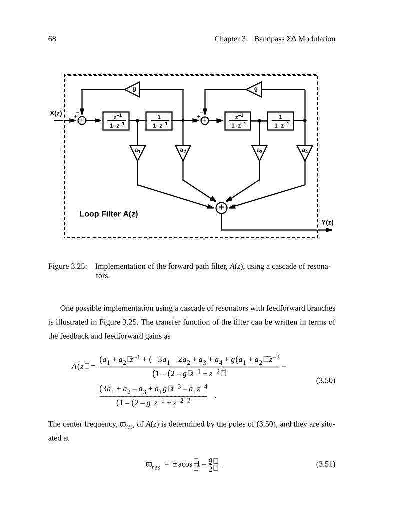
68 Chapter 3: BandpassΣ∆ Modulation
One possible implementation using a cascade of resonators with feedforward branches
is illustrated in Figure3.25. The transfer function of the filter can be written in terms of
the feedback and feedforward gains as
(3.50)
The center frequency, ωres, of A(z) is determined by the poles of (3.50), and they are situ-
ated at
. (3.51)
Figure3.25: Implementation of the forward path filter, A(z), using a cascade of resona-tors.
++X(z)
Y(z)
– z–1
1–z–1
g
11–z–1
++–
z–1
1–z–1
g
11–z–1
a1 a2 a3 a4
+Loop Filter A(z)
A z( )a1 a2+( )z 1– 3a1– 2a2– a3 a4 g a1 a2+( )+ + +( )z 2–+
1 2 g–( )z 1–– z 2–+( )2--------------------------------------------------------------------------------------------------------------------------------------- +=
3a1 a2 a3– a1g+ +( )z 3– a1z 4––
1 2 g–( )z 1–– z 2–+( )2--------------------------------------------------------------------------------- .
ωres 1 g2---–
acos±=
3.4. Summary 69
With five degrees of freedom,a1 to a4, andg, the cascade-of-resonators structure can be
used to synthesize any fourth-order transfer function with poles coincident at±ωres, and
the structure can be generalized in straightforward manner to implement a 2Lth-order
transfer function. In addition, through the use of different feedback gains,g1 andg2, the
poles ofA(z) can be distributed within the signal passband rather than forcing them to be
coincident at the passband center frequency, ±ωres. This may be necessary if the oversam-
pling ratio is low and the quantization noise must be suppressed in a wide signal
bandwidth.
3.4 Summary
The design of high-resolution, Nyquist-rate A/D converters in a modern submicron tech-
nology is limited by device matching and the need to implement a precise antialiasing
filter with a narrow and well-defined transition band. These limitations can be circum-
vented by utilizing oversampling and feedback to shape the quantization noise away from
a narrow passband.
Traditionally, feedback modulators have been developed on the premise that quantiza-
tion noise is to be suppressed in a region centered at dc. However, by replacing the
constituent integrators of a lowpass modulator with resonators that realize an infinite gain
at fs/X, it is possible to suppress quantization noise in any portion of the spectrum from dc
to fs/2. Special design procedures must be followed in order to insure the stability of the
resulting bandpass noiseshaper. The bandpass architecture can be designed by applying
different lowpass-to-bandpass transformations to a lowpass prototype, or the modulator
can be designed to directly implement a specific noiseshaping function without relying on
a transformation from the lowpass domain.
The choice of architecture for a bandpass modulator is motivated by various design
criteria. For example, system-level characteristics such as overload recovery, signal excur-
sions at internal nodes, and out-of-band spectral coloration, are fundamentally impacted
by changes in the modulator architecture. In fact, behavioral simulations indicate that if
70 Chapter 3: BandpassΣ∆ Modulation
the signal passband is centered away fromfs/4, the output spectrum of the modulator will
not contain strong tones at dc for low-level input signals. However, the attendant increase
in circuit complexity required to implement a generalized cascade-of-resonators modula-
tor topology may preclude the use of a non-fs/4 architecture at sampling rates of tens of
MHz. These system- and circuit-level issues are explored further in the following chapter
when the design of a fourth-order, fs/4 modulator intended to digitize signal passbands
centered as high as 20 MHz is described.
71
Chapter
4 Design of aFourth-Order, fs/4Modulator
A number of experimental modulators based upon the bandpass architectures discussed in
the previous chapter have been reported for a variety of applications requiring the IF digi-
tization [50], [55], [56], [66]-[71] of narrowband (< 200 KHz) passbands. However, in
many of these modulators, those that achieve a dynamic range suitable for wireless sys-
tems (>70 dB) have also been limited to digitizing passbands centered at relatively low
intermediate frequencies of under 5 MHz [55], [69]. This limitation is due in part to the
fact that these modulators utilize anfs/4 architecture, which means that the modulator
must sample the input signal at a rate equal to four times the passband center frequency.
Therefore, with an IF of 5 MHz, the modulator sampling rate must already be 20 MHz. At
this frequency, the achievable dynamic range of the modulator can be influenced signifi-
cantly by analog circuit nonidealities such as incomplete and nonlinear settling of the
amplifier outputs. Extrapolating to the higher sampling rates necessary to digitize IF sig-
nals centered above 10 MHz, the performance of the modulator may be compromised to
such a degree that it is no longer viable for the intended application. This limits the utility
of bandpass modulators for wireless IF digitization because in receivers for RF carriers
between 1 and 2GHz, a second IF location between 10 and 20 MHz is typically chosen to
meet the competing requirements for image rejection and channel selectivity [72].
This chapter discusses the system-level design and analog circuit requirements for a
fourth-order, fs/4 modulator that digitizes a signal passband centered as high as 20MHz.
72 Chapter 4: Design of a Fourth-Order, fs/4 Modulator
Potential system-level problems such as large internal signal swings, offset, and timing jit-
ter are identified and analyzed. Following the discussion of the system architecture, the
primary circuit-level imperfections that impair the modulator at high sampling speeds are
considered. The impact of these circuit-related limitations is analyzed by considering their
effect on switched-capacitor biquadratic filters, which are the conventional building
blocks for discrete-time bandpass modulators. The penalty in the modulator’s dynamic
range is assessed by means of a behavioral model of the modulator that includes circuit
nonidealities. It is suggested that the demands imposed on the analog circuitry can be
reduced by a factor of two by implementing the modulator using a two-path topology.
4.1 System Design of anfs/4 Modulator Ar chitecture
In this work, canonicalfs/4 bandpass topologies that are derived using the dc-to-fs/4 trans-
formation, (3.23), are the topologies of choice for high-speed modulator designs because
these topologies can be implemented using comparatively simple circuit structures. More
specifically, fs/4 topologies derived using (3.23) can be implemented using two-path fil-
ters. A thorough discussion of the two-path design issues is delayed until the following
chapter, but it can be stated briefly that the main motivation for using a two-path topology
is that the path filters are clocked at only one-half of the effective sampling frequency of
the modulator. Therefore, for a given sampling frequency, the allowable settling time for
each analog block is increased by a factor of two. In this manner, the time allotted for set-
tling in the analog circuitry can be increased by a greater margin than by placing the signal
passband closer tofs/2 and operating the modulator at a lower sampling frequency. The
remainder of this chapter is devoted to a discussion of the system-level modulator design
and an analysis of the analog circuit nonidealities that motivate the use of a two-path
topology.
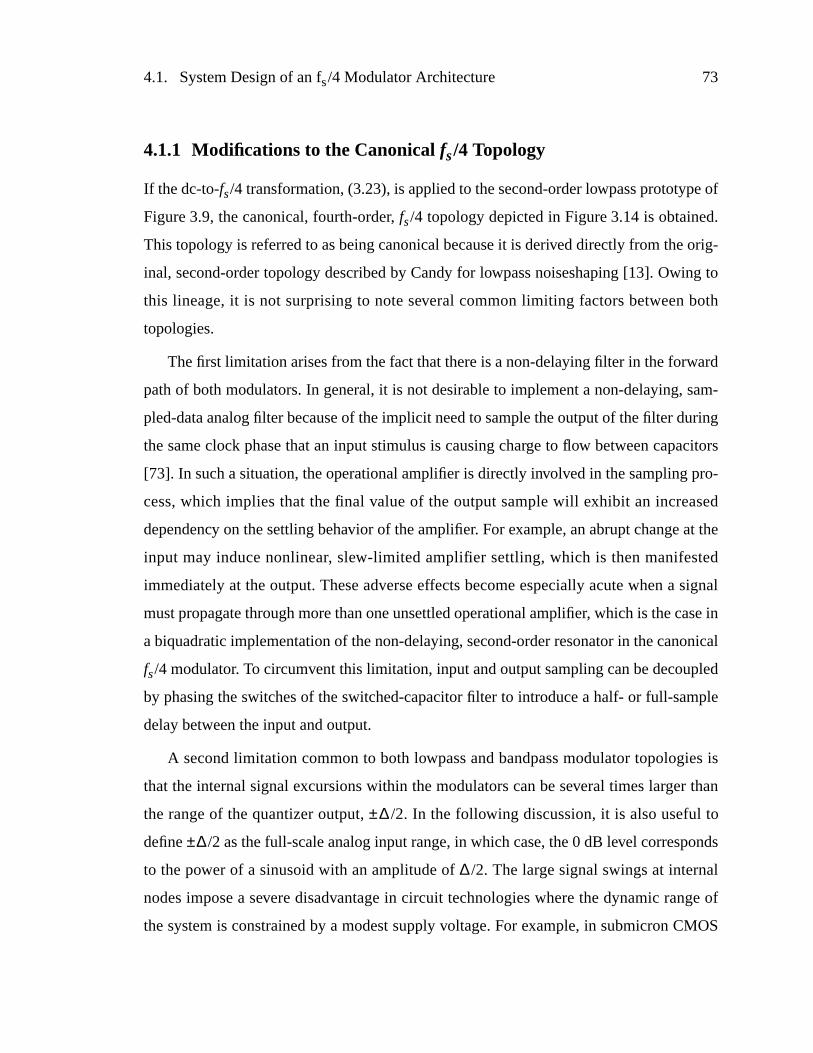
4.1. System Design of an fs/4 Modulator Architecture 73
4.1.1 Modifications to the Canonicalfs/4 Topology
If the dc-to-fs/4 transformation, (3.23), is applied to the second-order lowpass prototype of
Figure3.9, the canonical, fourth-order, fs/4 topology depicted in Figure3.14 is obtained.
This topology is referred to as being canonical because it is derived directly from the orig-
inal, second-order topology described by Candy for lowpass noiseshaping [13]. Owing to
this lineage, it is not surprising to note several common limiting factors between both
topologies.
The first limitation arises from the fact that there is a non-delaying filter in the forward
path of both modulators. In general, it is not desirable to implement a non-delaying, sam-
pled-data analog filter because of the implicit need to sample the output of the filter during
the same clock phase that an input stimulus is causing charge to flow between capacitors
[73]. In such a situation, the operational amplifier is directly involved in the sampling pro-
cess, which implies that the final value of the output sample will exhibit an increased
dependency on the settling behavior of the amplifier. For example, an abrupt change at the
input may induce nonlinear, slew-limited amplifier settling, which is then manifested
immediately at the output. These adverse effects become especially acute when a signal
must propagate through more than one unsettled operational amplifier, which is the case in
a biquadratic implementation of the non-delaying, second-order resonator in the canonical
fs/4 modulator. To circumvent this limitation, input and output sampling can be decoupled
by phasing the switches of the switched-capacitor filter to introduce a half- or full-sample
delay between the input and output.
A second limitation common to both lowpass and bandpass modulator topologies is
that the internal signal excursions within the modulators can be several times larger than
the range of the quantizer output,±∆ /2. In the following discussion, it is also useful to
define±∆/2 as the full-scale analog input range, in which case, the 0 dB level corresponds
to the power of a sinusoid with an amplitude of∆ /2. The large signal swings at internal
nodes impose a severe disadvantage in circuit technologies where the dynamic range of
the system is constrained by a modest supply voltage. For example, in submicron CMOS
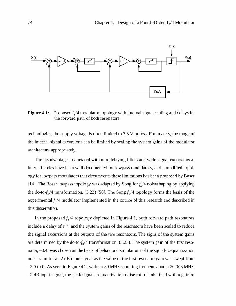
74 Chapter 4: Design of a Fourth-Order, fs/4 Modulator
technologies, the supply voltage is often limited to 3.3 V or less. Fortunately, the range of
the internal signal excursions can be limited by scaling the system gains of the modulator
architecture appropriately.
The disadvantages associated with non-delaying filters and wide signal excursions at
internal nodes have been well documented for lowpass modulators, and a modified topol-
ogy for lowpass modulators that circumvents these limitations has been proposed by Boser
[14]. The Boser lowpass topology was adapted by Song forfs/4 noiseshaping by applying
the dc-to-fs/4 transformation, (3.23) [56]. The Songfs/4 topology forms the basis of the
experimentalfs/4 modulator implemented in the course of this research and described in
this dissertation.
In the proposedfs/4 topology depicted in Figure4.1, both forward path resonators
include a delay ofz–2, and the system gains of the resonators have been scaled to reduce
the signal excursions at the outputs of the two resonators. The signs of the system gains
are determined by the dc-to-fs/4 transformation, (3.23). The system gain of the first reso-
nator, –0.4, was chosen on the basis of behavioral simulations of the signal-to-quantization
noise ratio for a –2 dB input signal as the value of the first resonator gain was swept from
–2.0 to 0. As seen in Figure4.2, with an 80MHz sampling frequency and a 20.003MHz,
–2 dB input signal, the peak signal-to-quantization noise ratio is obtained with a gain of
Figure 4.1: Proposedfs/4 modulator topology with internal signal scaling and delays inthe forward path of both resonators.
+X(z)
E(z)
Y(z)+
+
+
+
+
–z–2
+
–z–2–0.4 0.5+ + +
D/A
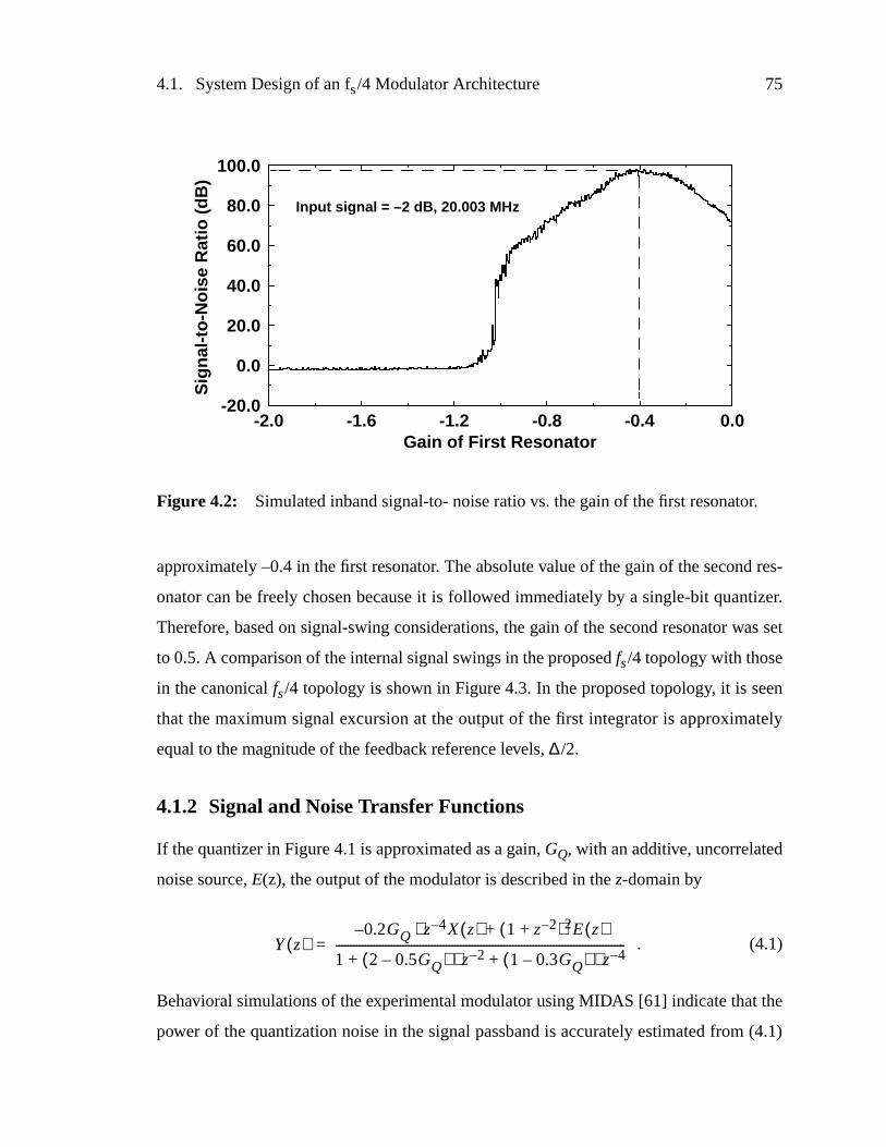
4.1. System Design of an fs/4 Modulator Architecture 75
approximately –0.4 in the first resonator. The absolute value of the gain of the second res-
onator can be freely chosen because it is followed immediately by a single-bit quantizer.
Therefore, based on signal-swing considerations, the gain of the second resonator was set
to 0.5. A comparison of the internal signal swings in the proposedfs/4 topology with those
in the canonicalfs/4 topology is shown in Figure4.3. In the proposed topology, it is seen
that the maximum signal excursion at the output of the first integrator is approximately
equal to the magnitude of the feedback reference levels,∆/2.
4.1.2 Signal and Noise Transfer Functions
If the quantizer in Figure4.1 is approximated as a gain,GQ, with an additive, uncorrelated
noise source,E(z), the output of the modulator is described in thez-domain by
. (4.1)
Behavioral simulations of the experimental modulator using MIDAS [61] indicate that the
power of the quantization noise in the signal passband is accurately estimated from (4.1)
Figure 4.2: Simulated inband signal-to- noise ratio vs. the gain of the first resonator.
-2.0 -1.6 -1.2 -0.8 -0.4 0.0-20.0
0.0
20.0
40.0
60.0
80.0
100.0
Gain of First Resonator
Sig
nal-t
o-N
oise
Rat
io (
dB)
Input signal = –2 dB, 20.003 MHz
Y z( )0.2GQ z⋅ 4– X z( ) 1 z 2–+( )2E z( )+–
1 2 0.5GQ–( ) z⋅ 2– 1 0.3GQ–( ) z 4–⋅++----------------------------------------------------------------------------------------------------=
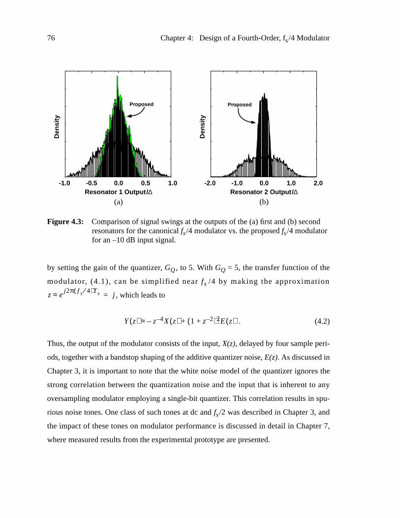
76 Chapter 4: Design of a Fourth-Order, fs/4 Modulator
by setting the gain of the quantizer, GQ, to 5. With GQ = 5, the transfer function of the
modulator, (4.1), can be simplified nearfs /4 by making the approximation
, which leads to
. (4.2)
Thus, the output of the modulator consists of the input,X(z), delayed by four sample peri-
ods, together with a bandstop shaping of the additive quantizer noise,E(z). As discussed in
Chapter 3, it is important to note that the white noise model of the quantizer ignores the
strong correlation between the quantization noise and the input that is inherent to any
oversampling modulator employing a single-bit quantizer. This correlation results in spu-
rious noise tones. One class of such tones at dc andfs/2 was described in Chapter 3, and
the impact of these tones on modulator performance is discussed in detail in Chapter 7,
where measured results from the experimental prototype are presented.
Figure 4.3: Comparison of signal swings at the outputs of the (a) first and (b) secondresonators for the canonicalfs/4 modulator vs. the proposedfs/4 modulatorfor an –10 dB input signal.
(a) (b)
-1.0 -0.5 0.0 0.5 1.0 -2.0 -1.0 0.0 1.0 2.0
Den
sity
Den
sity
Resonator 1 Output /∆ Resonator 2 Output /∆
Proposed Proposed
z ej2π f s 4⁄( )Ts≈ j=
Y z( ) z 4– X z( )– 1 z 2–+( )2E z( )+≈
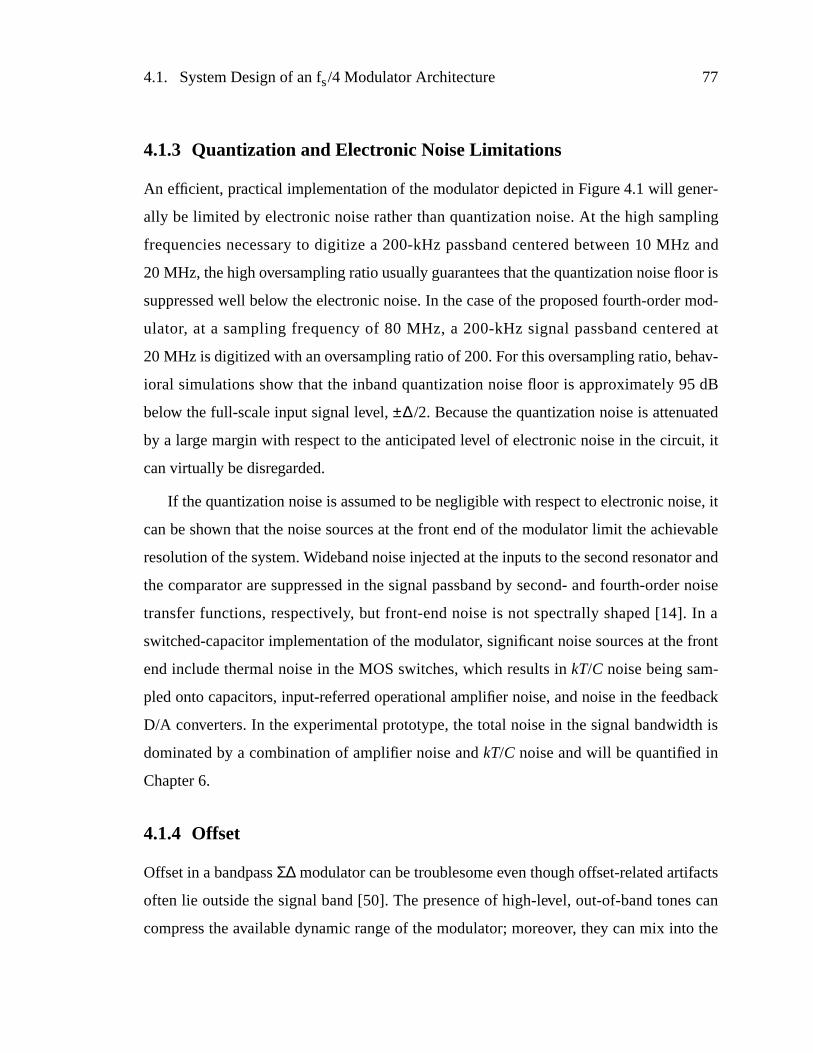
4.1. System Design of an fs/4 Modulator Architecture 77
4.1.3 Quantization and Electronic Noise Limitations
An efficient, practical implementation of the modulator depicted in Figure4.1 will gener-
ally be limited by electronic noise rather than quantization noise. At the high sampling
frequencies necessary to digitize a 200-kHz passband centered between 10MHz and
20MHz, the high oversampling ratio usually guarantees that the quantization noise floor is
suppressed well below the electronic noise. In the case of the proposed fourth-order mod-
ulator, at a sampling frequency of 80 MHz, a 200-kHz signal passband centered at
20MHz is digitized with an oversampling ratio of 200. For this oversampling ratio, behav-
ioral simulations show that the inband quantization noise floor is approximately 95dB
below the full-scale input signal level, ±∆/2. Because the quantization noise is attenuated
by a large margin with respect to the anticipated level of electronic noise in the circuit, it
can virtually be disregarded.
If the quantization noise is assumed to be negligible with respect to electronic noise, it
can be shown that the noise sources at the front end of the modulator limit the achievable
resolution of the system. Wideband noise injected at the inputs to the second resonator and
the comparator are suppressed in the signal passband by second- and fourth-order noise
transfer functions, respectively, but front-end noise is not spectrally shaped [14]. In a
switched-capacitor implementation of the modulator, significant noise sources at the front
end include thermal noise in the MOS switches, which results inkT/C noise being sam-
pled onto capacitors, input-referred operational amplifier noise, and noise in the feedback
D/A converters. In the experimental prototype, the total noise in the signal bandwidth is
dominated by a combination of amplifier noise and kT/C noise and will be quantified in
Chapter6.
4.1.4 Offset
Offset in a bandpassΣ∆ modulator can be troublesome even though offset-related artifacts
often lie outside the signal band [50]. The presence of high-level, out-of-band tones can
compress the available dynamic range of the modulator; moreover, they can mix into the
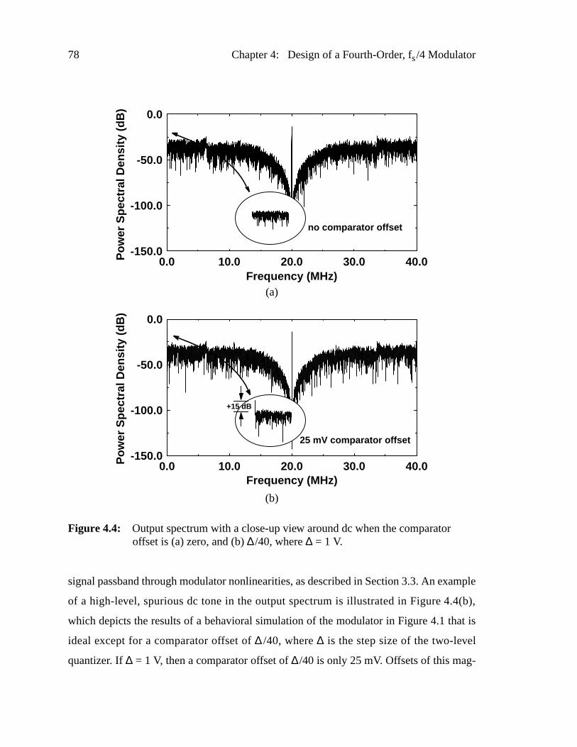
78 Chapter 4: Design of a Fourth-Order, fs/4 Modulator
signal passband through modulator nonlinearities, as described in Section 3.3. An example
of a high-level, spurious dc tone in the output spectrum is illustrated in Figure4.4(b),
which depicts the results of a behavioral simulation of the modulator in Figure4.1 that is
ideal except for a comparator offset of∆ /40, where∆ is the step size of the two-level
quantizer. If ∆ = 1 V, then a comparator offset of∆/40 is only 25mV. Offsets of this mag-
Figure 4.4: Output spectrum with a close-up view around dc when the comparatoroffset is (a) zero, and (b)∆/40, where∆ = 1 V.
0.0 10.0 20.0 30.0 40.0-150.0
-100.0
-50.0
0.0
0.0 10.0 20.0 30.0 40.0-150.0
-100.0
-50.0
0.0
Frequency (MHz)
Pow
er S
pect
ral D
ensi
ty (
dB)
Frequency (MHz)
Pow
er S
pect
ral D
ensi
ty (
dB)
(a)
(b)
no comparator offset
25 mV comparator offset
+15 dB
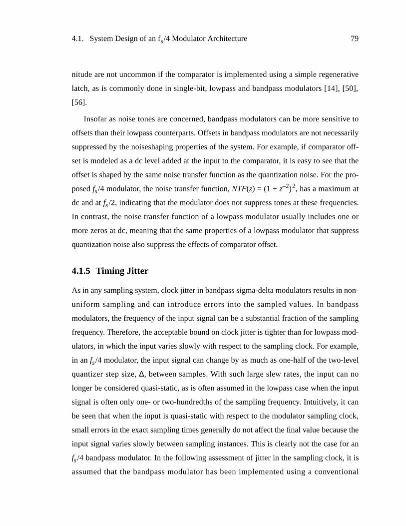
4.1. System Design of an fs/4 Modulator Architecture 79
nitude are not uncommon if the comparator is implemented using a simple regenerative
latch, as is commonly done in single-bit, lowpass and bandpass modulators [14], [50],
[56].
Insofar as noise tones are concerned, bandpass modulators can be more sensitive to
offsets than their lowpass counterparts. Offsets in bandpass modulators are not necessarily
suppressed by the noiseshaping properties of the system. For example, if comparator off-
set is modeled as a dc level added at the input to the comparator, it is easy to see that the
offset is shaped by the same noise transfer function as the quantization noise. For the pro-
posedfs/4 modulator, the noise transfer function,NTF(z) = (1 +z–2)2, has a maximum at
dc and atfs/2, indicating that the modulator does not suppress tones at these frequencies.
In contrast, the noise transfer function of a lowpass modulator usually includes one or
more zeros at dc, meaning that the same properties of a lowpass modulator that suppress
quantization noise also suppress the effects of comparator offset.
4.1.5 Timing Jitter
As in any sampling system, clock jitter in bandpass sigma-delta modulators results in non-
uniform sampling and can introduce errors into the sampled values. In bandpass
modulators, the frequency of the input signal can be a substantial fraction of the sampling
frequency. Therefore, the acceptable bound on clock jitter is tighter than for lowpass mod-
ulators, in which the input varies slowly with respect to the sampling clock. For example,
in anfs/4 modulator, the input signal can change by as much as one-half of the two-level
quantizer step size,∆, between samples. With such large slew rates, the input can no
longer be considered quasi-static, as is often assumed in the lowpass case when the input
signal is often only one- or two-hundredths of the sampling frequency. Intuitively, it can
be seen that when the input is quasi-static with respect to the modulator sampling clock,
small errors in the exact sampling times generally do not affect the final value because the
input signal varies slowly between sampling instances. This is clearly not the case for an
fs/4 bandpass modulator. In the following assessment of jitter in the sampling clock, it is
assumed that the bandpass modulator has been implemented using a conventional
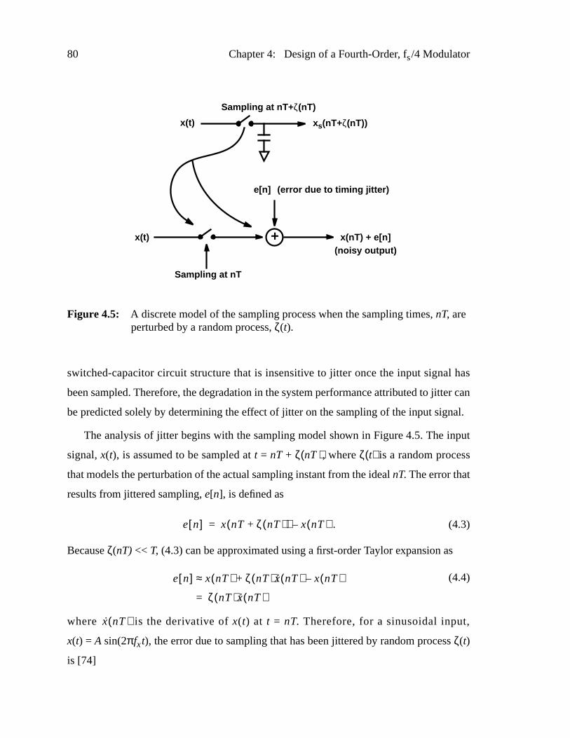
80 Chapter 4: Design of a Fourth-Order, fs/4 Modulator
switched-capacitor circuit structure that is insensitive to jitter once the input signal has
been sampled. Therefore, the degradation in the system performance attributed to jitter can
be predicted solely by determining the effect of jitter on the sampling of the input signal.
The analysis of jitter begins with the sampling model shown in Figure4.5. The input
signal,x(t), is assumed to be sampled att = nT + ζ(nT), whereζ(t) is a random process
that models the perturbation of the actual sampling instant from the idealnT. The error that
results from jittered sampling,e[n], is defined as
. (4.3)
Becauseζ(nT) << T, (4.3) can be approximated using a first-order Taylor expansion as
(4.4)
where is the derivative of x(t) at t = nT. Therefore, for a sinusoidal input,
x(t) = A sin(2πfxt), the error due to sampling that has been jittered by random processζ(t)
is [74]
Figure 4.5: A discrete model of the sampling process when the sampling times,nT, areperturbed by a random process,ζ(t).
+
e[n]
x(t) x(nT) + e[n]
Sampling at nT
(error due to timing jitter)
(noisy output)
Sampling at nT+ ζ(nT)
x(t) xs(nT+ζ(nT))
e n[ ] x nT ζ nT( )+( ) x nT( )–=
e n[ ] x nT( ) ζ nT( ) x nT( ) x nT( )–+≈
ζ nT( ) x nT( )=
x nT( )
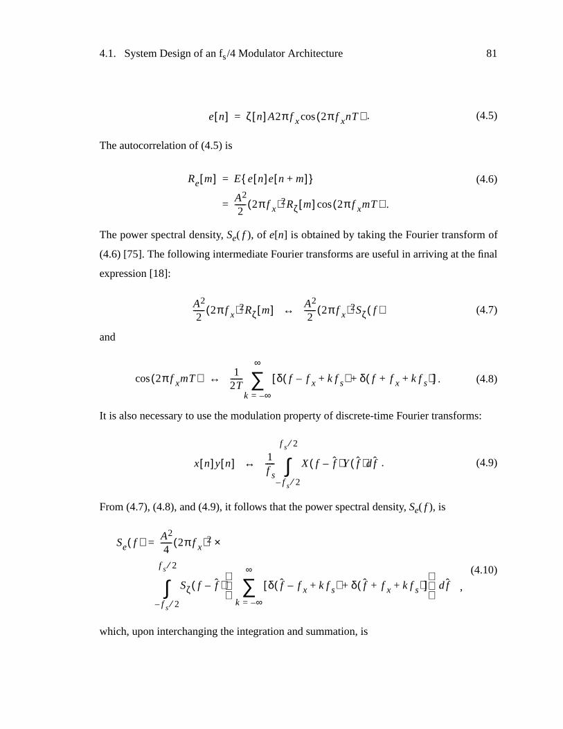
4.1. System Design of an fs/4 Modulator Architecture 81
. (4.5)
The autocorrelation of (4.5) is
(4.6)
The power spectral density, Se( f ), of e[n] is obtained by taking the Fourier transform of
(4.6) [75]. The following intermediate Fourier transforms are useful in arriving at the final
expression [18]:
(4.7)
and
. (4.8)
It is also necessary to use the modulation property of discrete-time Fourier transforms:
. (4.9)
From (4.7), (4.8), and (4.9), it follows that the power spectral density, Se( f ), is
(4.10)
which, upon interchanging the integration and summation, is
e n[ ] ζ n[ ] A2πf x 2πf xnT( )cos=
Re m[ ] E e n[ ]e n m+[ ] =
A2
2------ 2πf x( )2Rζ m[ ] 2πf xmT( )cos= .
A2
2------ 2πf x( )2Rζ m[ ] ↔ A2
2------ 2πf x( )2Sζ f( )
2πf xmT( ) 12T------- δ f f x– k f s+( ) δ f f x k f s+ +( )+[ ]
k ∞–=
∞
∑↔cos
x n[ ]y n[ ] 1f s----- X f f–( )Y f( ) fd
f s 2⁄–
f s 2⁄
∫↔
Se f( ) A2
4------ 2πf x( )2 ×=
Sζ f f–( ) δ f f x– k f s+( ) δ f f x k f s+ +( )+[ ]k ∞–=
∞
∑
fd
f s 2⁄–
f s 2⁄
∫ ,
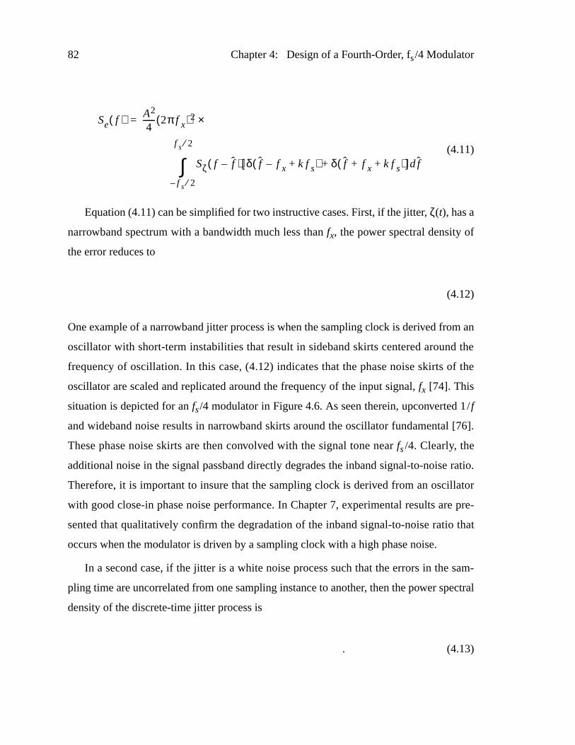
82 Chapter 4: Design of a Fourth-Order, fs/4 Modulator
(4.11)
Equation (4.11) can be simplified for two instructive cases. First, if the jitter, ζ(t), has a
narrowband spectrum with a bandwidth much less thanfx, the power spectral density of
the error reduces to
(4.12)
One example of a narrowband jitter process is when the sampling clock is derived from an
oscillator with short-term instabilities that result in sideband skirts centered around the
frequency of oscillation. In this case, (4.12) indicates that the phase noise skirts of the
oscillator are scaled and replicated around the frequency of the input signal,fx [74]. This
situation is depicted for anfs/4 modulator in Figure4.6. As seen therein, upconverted 1/ f
and wideband noise results in narrowband skirts around the oscillator fundamental [76].
These phase noise skirts are then convolved with the signal tone nearfs/4. Clearly, the
additional noise in the signal passband directly degrades the inband signal-to-noise ratio.
Therefore, it is important to insure that the sampling clock is derived from an oscillator
with good close-in phase noise performance. In Chapter 7, experimental results are pre-
sented that qualitatively confirm the degradation of the inband signal-to-noise ratio that
occurs when the modulator is driven by a sampling clock with a high phase noise.
In a second case, if the jitter is a white noise process such that the errors in the sam-
pling time are uncorrelated from one sampling instance to another, then the power spectral
density of the discrete-time jitter process is
. (4.13)
Se f( ) A2
4------ 2πf x( )2 ×=
Sζ f f–( ) δ f f x– k f s+( ) δ f f x k f s+ +( )+[ ] fd
f s 2⁄–
f s 2⁄
∫î
k ∞–=
∞
∑ .
Se f( ) A2
4------ 2πf x( )2× Sζ f f x–( ) Sζ f f x+( )+[ ]×= ,
f s
2----- f
f s
2-----< <– .
Sζ f( )σζ
2
f s------= ,
f s
2----- f
f s
2-----< <–
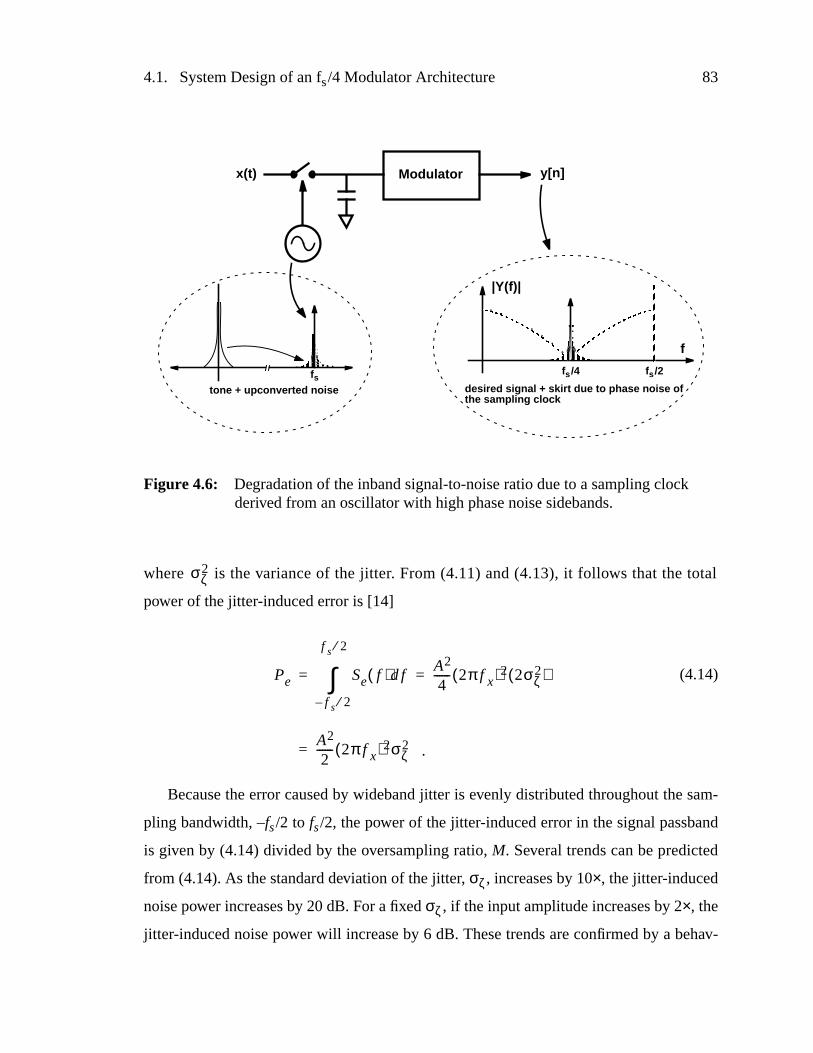
4.1. System Design of an fs/4 Modulator Architecture 83
where is the variance of the jitter. From (4.11) and (4.13), it follows that the total
power of the jitter-induced error is [14]
(4.14)
Because the error caused by wideband jitter is evenly distributed throughout the sam-
pling bandwidth, –fs/2 to fs/2, the power of the jitter-induced error in the signal passband
is given by (4.14) divided by the oversampling ratio,M. Several trends can be predicted
from (4.14). As the standard deviation of the jitter, σζ , increases by 10×, the jitter-induced
noise power increases by 20 dB. For a fixedσζ , if the input amplitude increases by 2×, the
jitter-induced noise power will increase by 6 dB. These trends are confirmed by a behav-
Figure 4.6: Degradation of the inband signal-to-noise ratio due to a sampling clockderived from an oscillator with high phase noise sidebands.
Modulatorx(t)
desired signal + skirt due to phase noise of
fs /4
tone + upconverted noisefs fs /2
y[n]
|Y(f)|
f
the sampling clock
σζ2
Pe Se f( ) fd
f s 2⁄–
f s 2⁄
∫ A2
4------ 2πf x( )2 2σζ
2( )= =
A2
2------ 2πf x( )2σζ
2= .
84 Chapter 4: Design of a Fourth-Order, fs/4 Modulator
ioral simulation of the modulator in Figure4.1 in which jitter is modeled by adding a
random errorζ, which has a zero mean and variance, to the ideal sampling times,nT.
Wideband noise is also added at the input to simulate the effect of kT/C noise. As indi-
cated in Figure4.7, when the jitter-induced noise begins to predominate over thekT/C
noise floor, it is seen that the noise floor increases by 20 dB for every 10× increase in the
standard deviation of the jitter. It is also observed that for a given jitter standard deviation,
the noise floor increases by 6dB as the amplitude of the input signal is doubled.
4.2 High Frequency Impairments
At high sampling speeds, the performance of the proposed fourth-order modulator
depicted in Figure4.1 is limited primarily by the nonideal behavior of the bandpass reso-
nators. The ideal resonator has a biquadratic transfer function of
Figure 4.7: Behavioral simulation showing the broad increase in the noise floor thatoccurs as the standard deviation of the jitter increases.
10-11 10-10 10-9-100.0
-80.0
-60.0
-40.0
10-12
Jitter Standard Deviation (s)
Input signal = 20.003 MHz, power as shown
P =–16 dB
P = –10 dB
P = –4 dB
kT/C noise floor
Noi
se F
loor
(dB
)
σζ2
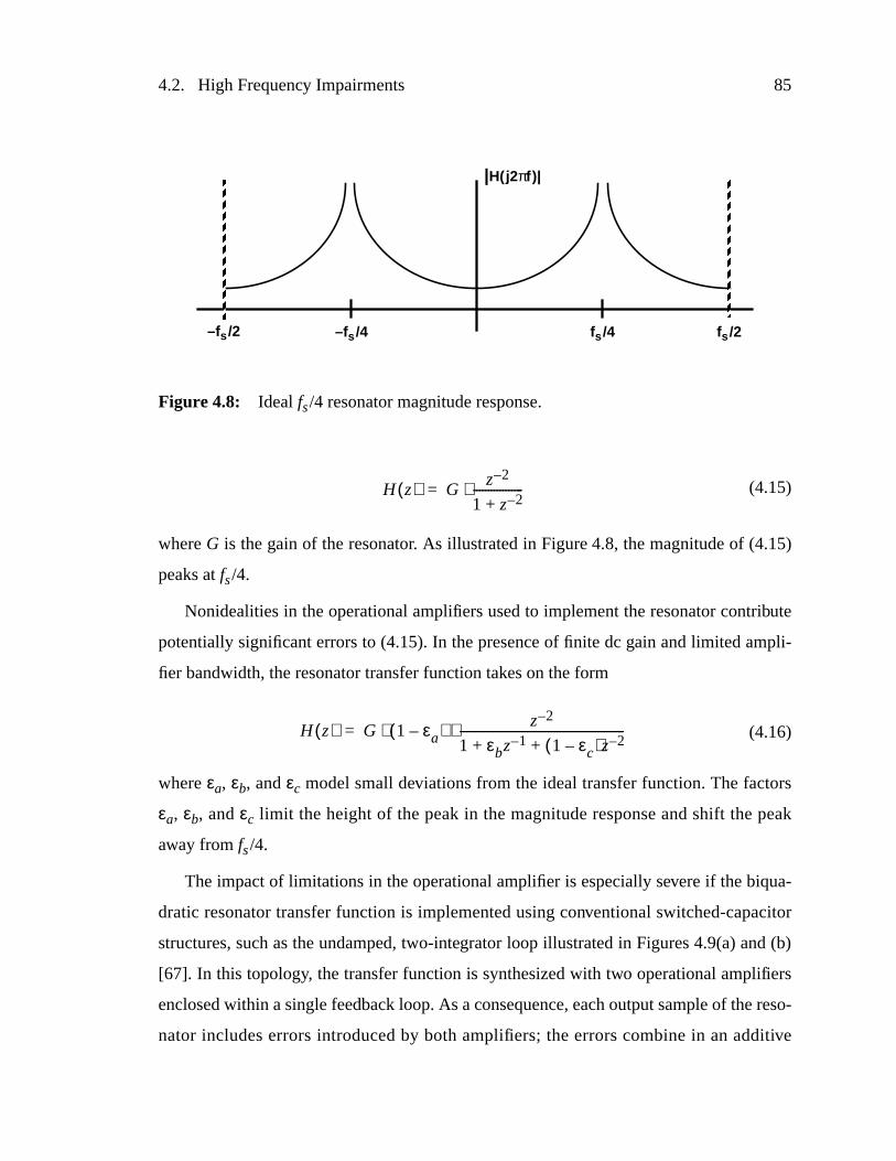
4.2. High Frequency Impairments 85
(4.15)
whereG is the gain of the resonator. As illustrated in Figure4.8, the magnitude of (4.15)
peaks atfs/4.
Nonidealities in the operational amplifiers used to implement the resonator contribute
potentially significant errors to (4.15). In the presence of finite dc gain and limited ampli-
fier bandwidth, the resonator transfer function takes on the form
(4.16)
whereεa, εb, andεc model small deviations from the ideal transfer function. The factors
εa, εb, andεc limit the height of the peak in the magnitude response and shift the peak
away fromfs/4.
The impact of limitations in the operational amplifier is especially severe if the biqua-
dratic resonator transfer function is implemented using conventional switched-capacitor
structures, such as the undamped, two-integrator loop illustrated in Figures 4.9(a) and (b)
[67]. In this topology, the transfer function is synthesized with two operational amplifiers
enclosed within a single feedback loop. As a consequence, each output sample of the reso-
nator includes errors introduced by both amplifiers; the errors combine in an additive
H z( ) Gz 2–
1 z 2–+-----------------⋅=
Figure 4.8: Idealfs/4 resonator magnitude response.
fs /4–fs /4–fs /2 fs /2
|H(j2πf )|
H z( ) G 1 εa–( ) z 2–
1 εbz 1– 1 εc–( )z 2–+ +--------------------------------------------------------⋅ ⋅=
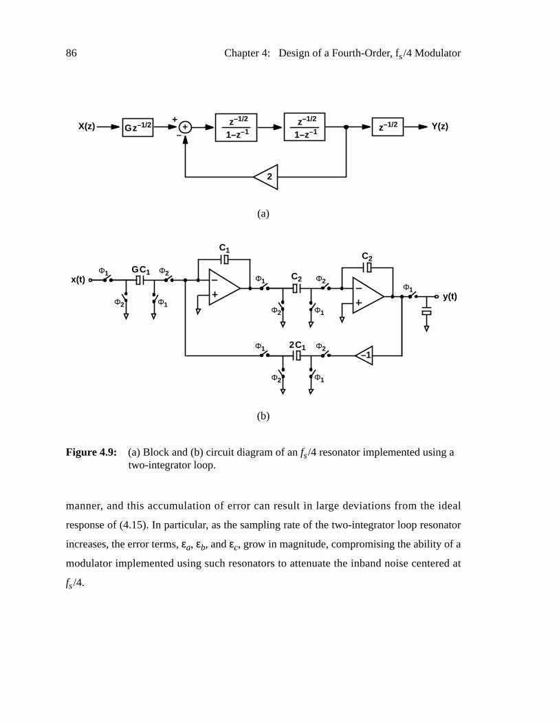
86 Chapter 4: Design of a Fourth-Order, fs/4 Modulator
manner, and this accumulation of error can result in large deviations from the ideal
response of (4.15). In particular, as the sampling rate of the two-integrator loop resonator
increases, the error terms,εa, εb, andεc, grow in magnitude, compromising the ability of a
modulator implemented using such resonators to attenuate the inband noise centered at
fs/4.
Figure 4.9: (a) Block and (b) circuit diagram of anfs/4 resonator implemented using atwo-integrator loop.
++
X(z) Y(z)–
Gz–1/2 z–1/2
1–z–1
2
z–1/2 z–1/2
1–z–1
(a)
(b)
Φ1
Φ1Φ2
Φ2GC1
Φ1
Φ1Φ2
Φ22C1
Φ1
Φ1Φ2
Φ2C2
Φ1
–1
C1C2
x(t)
y(t)
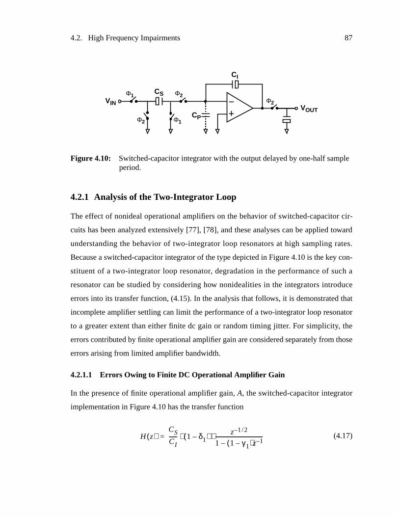
4.2. High Frequency Impairments 87
4.2.1 Analysis of the Two-Integrator Loop
The effect of nonideal operational amplifiers on the behavior of switched-capacitor cir-
cuits has been analyzed extensively [77], [78], and these analyses can be applied toward
understanding the behavior of two-integrator loop resonators at high sampling rates.
Because a switched-capacitor integrator of the type depicted in Figure4.10 is the key con-
stituent of a two-integrator loop resonator, degradation in the performance of such a
resonator can be studied by considering how nonidealities in the integrators introduce
errors into its transfer function, (4.15). In the analysis that follows, it is demonstrated that
incomplete amplifier settling can limit the performance of a two-integrator loop resonator
to a greater extent than either finite dc gain or random timing jitter. For simplicity, the
errors contributed by finite operational amplifier gain are considered separately from those
errors arising from limited amplifier bandwidth.
4.2.1.1 Err ors Owing to Finite DC Operational Amplifier Gain
In the presence of finite operational amplifier gain, A, the switched-capacitor integrator
implementation in Figure4.10 has the transfer function
(4.17)
Figure 4.10: Switched-capacitor integrator with the output delayed by one-half sampleperiod.
VIN
Φ1
Φ1Φ2
Φ2CS
Φ2
CI
VOUTCP
H z( )CS
CI------ 1 δ1–( ) z 1 2/–
1 1 γ1–( )z 1––------------------------------------⋅ ⋅=
88 Chapter 4: Design of a Fourth-Order, fs/4 Modulator
where the termsδ1 andγ1 model perturbations in the gain and pole locations of the inte-
grator, respectively, and are given by
(4.18)
and
. (4.19)
The effect of finite amplifier gain on the resonator of Figure4.9(b) is assessed by mod-
eling the two, nominally identical, switched-capacitor integrators with (4.17) and
independent error terms,δ1, γ1, δ2, andγ2. The system gains of both integrators,CS/CI, are
chosen to be one. With this representation, the nonideal transfer function of the resonator
is approximated by
(4.20)
when second-order terms are neglected since they are much less than one. Errorsδ1, γ1, δ2,
andγ2 have the effect of causing the poles ofH(z) to shift away from± fs/4, and off of the
unit circle (|z| = 1). The new pole locations are
. (4.21)
For small perturbations, namelyδ1, γ1, δ2, andγ2 << 1, the pole locations, (4.21), simplify
to
δ11A--- 1
CS
CI------+
=
γ1
1A---
CS
CI------
11A--- 1
CS
CI------+
+
-----------------------------------=
H z( ) 1 δ1– δ2–( ) z 2–
1 γ1 γ2 2δ1– 2δ2–+( )z 1– 1 γ1– γ2–( )z 2–+ +-------------------------------------------------------------------------------------------------------------------⋅=
p1 p2,2δ1 2δ2 γ1– γ2– γ1 γ2 2δ1– 2δ2–+( )2 4 1 γ1– γ2–( )–±+
2 1 γ1– γ2–( )----------------------------------------------------------------------------------------------------------------------------------------------------------=
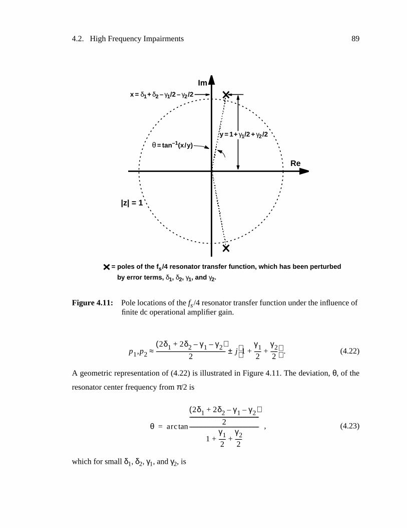
4.2. High Frequency Impairments 89
. (4.22)
A geometric representation of (4.22) is illustrated in Figure4.11. The deviation,θ, of the
resonator center frequency from π/2 is
, (4.23)
which for smallδ1, δ2, γ1, and γ2, is
p1 p2,2δ1 2δ2 γ1– γ2–+( )
2---------------------------------------------------- j 1
γ1
2-----
γ2
2-----+ +
±≈
Figure 4.11: Pole locations of thefs/4 resonator transfer function under the influence offinite dc operational amplifier gain.
Re
Im
|z| = 1
x = δ1+ δ2 – γ1/2 – γ2/2
y = 1+ γ1/2 + γ2/2
θ= tan–1(x /y)
= poles of the f s /4 resonator transf er function, whic h has been per turbed
by err or terms, δ1, δ2, γ1, and γ2.
θ arc
2δ1 2δ2 γ1– γ2–+( )2
----------------------------------------------------
1γ1
2-----
γ2
2-----+ +
----------------------------------------------------tan=
90 Chapter 4: Design of a Fourth-Order, fs/4 Modulator
. (4.24)
Thus, for small perturbationsδ1, γ1, δ2, andγ2, the error in the resonator center frequency,
fo, is
, (4.25)
so the fractional deviation in the resonator center frequency is
. (4.26)
If the switched-capacitor integrators in Figure4.9(b) are implemented with opera-
tional amplifiers having a nominal dc gain of 60 dB, it follows from (4.20) and (4.26) that
the magnitude peak of the resonator transfer function shifts by only 0.2% offo, or 40 kHz,
when its ideal center frequency is 20 MHz. Because of a fortuitous partial cancellation in
(4.26) between perturbation termsγ1, γ2 andδ1, δ2, the deviation in fo is relatively small,
even with a modest amplifier gain of only 60 dB. Within the context of a bandpass modu-
lator, this shift in the peak of the magnitude response of the resonator results in a
corresponding shift in the minimum of the noise transfer function away fromfs/4.
The increase in inband noise in the fourth-order modulator of Figure4.1 that results
from finite amplifier gain has been estimated by means of behavioral simulations that
model the constituent resonators with (4.20). Resonator perturbation terms,δ1, γ1 andδ2,
γ2, were determined by assuming an amplifier gain of 60 dB. In a 200-kHz passband cen-
tered atfs/4, the simulations show that the loss in dynamic range is approximately 5 dB in
a modulator with performance that is limited solely by quantization noise.
In practice, the dynamic range of a modulator is often limited by circuit, rather than
quantization noise. In such cases, the noise floor within the signal passband is determined
by noise introduced at the input to the modulator, since this noise is not attenuated by
noiseshaping. Sources of this unshaped noise include thermal noise in the first resonator,
θ δ1 δ2
γ1
2-----–
γ2
2-----–+≈
∆ f o θ–f s
2π------×≈ θ
4 f o
2π---------×–
γ1
2-----
γ2
2----- δ1– δ2–+
2 f o
π---------×= =
f o∆f o
---------γ1 γ2 2δ1– 2δ2–+
π-----------------------------------------------≈
4.2. High Frequency Impairments 91
as well askT/C noise from the input sampling network. When the shaped quantization
noise lies well below the noise floor within the passband, small shifts in the exact mini-
mum of the noise transfer function have a negligible influence on the total inband noise.
This is not true, however, if the fractional shift info becomes large enough to begin shift-
ing the large out-of-band quantization noise into the signal passband.
The above analysis is limited by the assumption that the response of the amplifier is
linear across its entire output range. Under this assumption, a dc gain of only 60dB is suf-
ficient to avoid any appreciable loss in the dynamic range. In practice, however, higher dc
gains may be needed to suppress harmonic distortion in the integrators that can result from
nonlinearity in the amplifier transfer characteristic.
4.2.1.2 Err ors Owing to Finite Operational Amplifier Bandwidth
In the presence of limited operational amplifier bandwidth, the switched-capacitor integra-
tor of Figure4.10 suffers from incomplete settling. If the integrator is assumed to settle
linearly with a single-pole response, incomplete settling only manifests itself as an inte-
grator gain error [14]. In this case, the transfer function of the integrator is
(4.27)
where gain error term,ε1, is
. (4.28)
T is the time allotted for settling, andτ is the closed-loop time constant of the integrator. If
the resonator is implemented using two-phase, non-overlapping clocks with 50% duty
cycles, the allowable settling time,T, is slightly less thanTs/2, where 1/Ts = fs, the sam-
pling frequency. The closed-loop time constant of the integrator, τ, is approximately
(4.29)
H z( )CS
CI------ 1 ε1–( ) z 1 2/–
1 z 1––----------------⋅ ⋅=
ε1 eT τ⁄–
=
τ 12πf u-------------
CS CI CP+ +
CI---------------------------------⋅≈
92 Chapter 4: Design of a Fourth-Order, fs/4 Modulator
wherefu is the unity-gain frequency of the operational amplifier andCP is the parasitic
capacitance at the input to the operational amplifier. As the sampling rate is increased, the
available settling time,T, decreases, and the gain error in (4.27) becomes increasingly
large.
As a caveat, it should be noted that, in practice, settling in switched-capacitor circuits
is rarely governed by a strictly linear, single-pole response. Rather, the settling process
usually includes a signal-dependent slewing component and is influenced by nondominant
poles of the amplifier [49], [79], as well as finite switch resistances in the switched-capac-
itor network. In such cases, errors in a switched-capacitor integrator due to incomplete
settling are understated by (4.27) and (4.28), with nonlinearities in the settling process not
even reflected in these expressions. For tractability, only linear settling is considered in
this analysis.
The effect of incomplete, but linear, integrator settling upon the resonator in
Figure4.9(b) can be assessed by modeling the two switched-capacitor integrators with
(4.27) and independent gain error parametersε1 andε2. When second-order terms are
neglected, the perturbed resonator transfer function is found to be
. (4.30)
From (4.30) and the analysis in the previous section for finite dc gain, it follows that the
fractional shift in resonator center frequency, fo, due to incomplete settling is
approximately
. (4.31)
The unfortunate implication of (4.28), (4.30), and (4.31) is that as the sampling frequency
is increased, thus decreasing the time allotted for settling,T, the fractional shift info
becomes larger, and the minimum of the modulator noise transfer function deviates by an
H z( ) 1 ε1– ε2–( ) z 2–
1 2ε1 2ε2+( )z 1–– z 2–+------------------------------------------------------------⋅=
f o∆f o
---------2ε1 2ε2+
π-----------------------–≈
4.3. Summary 93
increasing amount fromfs/4. Eventually, the noise minimum moves out of the signal pass-
band all together.
As an example, if the modulator shown in Figure4.1 operates at a sampling rate of
80MHz, from two-phase, non-overlapping clocks, less than 6 ns during each clock phase
is available for settling. If it is further assumed that a high bandwidth amplifier design
results in a closed-loop time constant,τ, of approximately 1.3 ns, the settling time is lim-
ited to roughly 4τ. From (4.30) and (4.31), it then follows that the center frequency of the
resonators will shift by –470 kHz. Under these assumptions, the penalty in dynamic range
can be assessed with MIDAS by modeling the constituent resonators using (4.30). Simula-
tions show that the dynamic range in a 200 kHz passband centered atfs/4 is reduced by
30dB if the modulator is limited by quantization noise.
As discussed in the previous subsection, the loss in dynamic range due to resonator
degradation will be less severe if a modulator is limited by thermal, rather than quantiza-
tion, noise. However, as is evident from (4.28) and (4.31), the shift in the minimum of the
noise transfer function fromfs/4 increases with increasing sampling rate, in contrast to the
shift that results from finite amplifier gain. Consequently, at the high sampling rates
needed to digitize signals at conventional radio IFs, the minimum of the noise transfer
function may shift by an amount large enough to move high levels of nominally
out-of-band quantization noise into the passband.
4.3 Summary
The design of a fourth-order, fs/4 modulator has been considered at the system level. Mod-
if ications to the canonicalfs/4 topology were proposed in order to address potential
limitations inherent in the architecture. Namely, a delay has been included in the forward
path of both resonators to improve the settling performance in a switched-capacitor imple-
mentation of the modulator. Also, the system gains of the resonators have been scaled to
constrain the signal swings at internal modulator nodes.
94 Chapter 4: Design of a Fourth-Order, fs/4 Modulator
Important system-level nonidealities were analyzed in order to assess their impact on
the performance of the proposedfs/4 modulator. It was shown that electronic noise and
timing jitter effectively raise the level of noise in the signal passband. If the noise is dis-
tributed equally over the sampling bandwidth, –fs/2 to fs/2, then the modulator attenuates
the amount of noise in the passband through oversampling or a combination of both over-
sampling and noiseshaping. However, in cases where the injected noise is concentrated
within the signal band, there may be a more severe loss in the inband signal-to-noise ratio.
This is the situation when the sampling clock is derived from an oscillator with a poor
close-in phase noise specification. In this case, the sideband skirts of the oscillator funda-
mental are scaled and replicated around the input signal. It was also demonstrated that a
modest amount of comparator offset could result in out-of-band tones that are 15 dB above
the noise floor near dc orfs/2. These tones are troublesome because they can limit the
dynamic range of the modulator and can mix with the input signal through nonlinearities
and fall into the passband.
In a switched-capacitor implementation, the effects of finite dc gain and limited set-
tling time in the operational amplifier were shown to directly degrade the transfer
functions of the resonators that constitute the modulator. As the sampling frequency is
increased, the error introduced by finite settling can cause the center frequency of the res-
onators to shift by several hundred kHz away from the center of the signal passband, thus
moving nominally out-of-band quantization noise into the passband. This degradation
becomes acute at the sampling frequencies necessary to digitize signals centered at fre-
quencies above 10 MHz. Fortunately, it is possible to attack this limitation through the use
of N-path filter topologies. As discussed in Section4.1, fs/4 modulators derived via the
dc-to-fs/4 transformation, (3.23), including the proposed topology depicted in Figure4.1,
can be easily partitioned into two independent time-interleaved paths that permit a dou-
bling of the allowable circuit settling time for a given sampling frequency. In the following
chapter, a review of N-path filter theory is presented, followed by a description of the cho-
sen two-path implementation of the proposedfs/4 modulator.
95
Chapter
5 N-Path Design Issues
The previous chapter proposed a system-level design for a fourth-order, fs/4 modulator
based upon the dc-to-fs/4 transformation, (3.23). It was also observed that a key motiva-
tion for choosing an architecture based on this transformation is that the resulting
modulator is especially suited for implementation using two-path circuits. The use of a
two-path topology allows the circuit blocks in the critical path of the modulator to operate
at a 2× slower sampling rate than the overall throughput of the modulator, which implies a
doubling of the allowable circuit settling time.
This chapter begins by introducing the general concept and motivation forN-path fil-
tering. The essential input-output relationships forN-path systems are stated, with detailed
derivations given in Appendix B. It is shown that by applyingN-path principles, the reso-
nators of the proposed fourth-order, fs/4 modulator can be implemented easily by
interleaving two highpass filters. This results in a simple resonator topology that resists
errors due to circuit nonidealities at high sampling speeds. However, this new topology is
still susceptible to errors arising from noise feedthrough, as well as the additional problem
of path mismatch. The impact of these nonidealities is analyzed. Finally, a complete block
diagram of the proposed two-path modulator implementation is shown, and its operation is
discussed.
5.1 N-Path Filter Theory
The design of a filter that must operate at high sampling rates and/or synthesize a very
selective passband may sometimes be simplified by partitioning the filter into N indepen-
dent paths, and clocking these paths with anN-phase, non-overlapping clock [80]-[85].
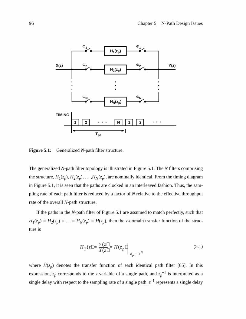
96 Chapter 5: N-Path Design Issues
The generalizedN-path filter topology is illustrated in Figure5.1. TheN filters comprising
the structure,H1(zp), H2(zp), … ,HN(zp), are nominally identical. From the timing diagram
in Figure5.1, it is seen that the paths are clocked in an interleaved fashion. Thus, the sam-
pling rate of each path filter is reduced by a factor ofN relative to the effective throughput
rate of the overallN-path structure.
If the paths in theN-path filter of Figure5.1 are assumed to match perfectly, such that
H1(zp) = H2(zp) = … = HN(zp) = H(zp), then thez-domain transfer function of the struc-
ture is
(5.1)
where H(zp) denotes the transfer function of each identical path filter [85]. In this
expression,zp corresponds to thez variable of a single path, andzp–1 is interpreted as a
single delay with respect to the sampling rate of a single path.z–1 represents a single delay
Figure 5.1: GeneralizedN-path filter structure.
H1(zp)
H2(zp)
HN(zp)
X(z) Y(z)
1 2 N 1 2
Tps
TIMING
Φ1 Φ1
Φ2 Φ2
ΦN ΦN
HT z( ) Y z( )X z( )----------- H zp( )= =
zp zN=
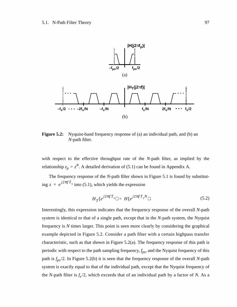
5.1. N-Path Filter Theory 97
with respect to the effective throughput rate of theN-path filter, as implied by the
relationshipzp = zN. A detailed derivation of (5.1) can be found in Appendix A.
The frequency response of theN-path filter shown in Figure5.1 is found by substitut-
ing into (5.1), which yields the expression
. (5.2)
Interestingly, this expression indicates that the frequency response of the overall N-path
system is identical to that of a single path, except that in theN-path system, the Nyquist
frequency is N times larger. This point is seen more clearly by considering the graphical
example depicted in Figure5.2. Consider a path filter with a certain highpass transfer
characteristic, such as that shown in Figure5.2(a). The frequency response of this path is
periodic with respect to the path sampling frequency, fps, and the Nyquist frequency of this
path isfps/2. In Figure5.2(b) it is seen that the frequency response of the overall N-path
system is exactly equal to that of the individual path, except that the Nyquist frequency of
theN-path filter is fs/2, which exceeds that of an individual path by a factor ofN. As a
z ej2πf Ts=
HT ej2πf Ts( ) H e
j2πf TsN( )=
Figure 5.2: Nyquist-band frequency response of (a) an individual path, and (b) anN-path filter.
–fps /2 fps /2
fs /22fs /Nfs /N
|HT(j2πf)|
–fs /2 –2fs /N –fs /N
(a)
(b)
|H(j2πfp)|
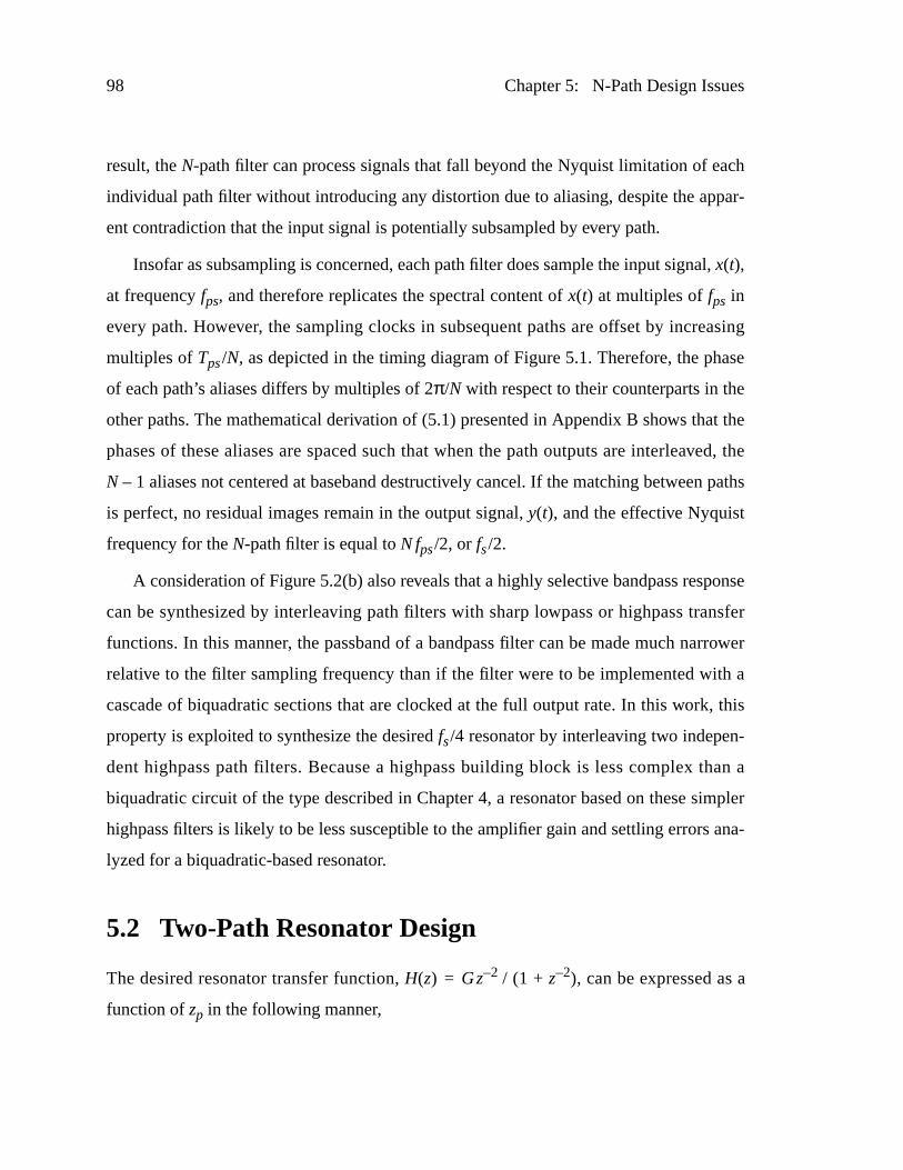
98 Chapter 5: N-Path Design Issues
result, theN-path filter can process signals that fall beyond the Nyquist limitation of each
individual path filter without introducing any distortion due to aliasing, despite the appar-
ent contradiction that the input signal is potentially subsampled by every path.
Insofar as subsampling is concerned, each path filter does sample the input signal,x(t),
at frequency fps, and therefore replicates the spectral content ofx(t) at multiples offps in
every path. However, the sampling clocks in subsequent paths are offset by increasing
multiples ofTps/N, as depicted in the timing diagram of Figure5.1. Therefore, the phase
of each path’s aliases differs by multiples of 2π/N with respect to their counterparts in the
other paths. The mathematical derivation of (5.1) presented in Appendix B shows that the
phases of these aliases are spaced such that when the path outputs are interleaved, the
N – 1 aliases not centered at baseband destructively cancel. If the matching between paths
is perfect, no residual images remain in the output signal,y(t), and the effective Nyquist
frequency for theN-path filter is equal toNfps/2, orfs/2.
A consideration of Figure5.2(b) also reveals that a highly selective bandpass response
can be synthesized by interleaving path filters with sharp lowpass or highpass transfer
functions. In this manner, the passband of a bandpass filter can be made much narrower
relative to the filter sampling frequency than if the filter were to be implemented with a
cascade of biquadratic sections that are clocked at the full output rate. In this work, this
property is exploited to synthesize the desiredfs/4 resonator by interleaving two indepen-
dent highpass path filters. Because a highpass building block is less complex than a
biquadratic circuit of the type described in Chapter 4, a resonator based on these simpler
highpass filters is likely to be less susceptible to the amplifier gain and settling errors ana-
lyzed for a biquadratic-based resonator.
5.2 Two-Path Resonator Design
The desired resonator transfer function,H(z) = Gz–2 / (1 + z–2), can be expressed as a
function ofzp in the following manner,
5.2. Two-Path Resonator Design 99
. (5.3)
Therefore, thefs/4 bandpass resonator can be naturally partitioned into a two-path struc-
ture consisting of two nominally identical highpass filters, as illustrated in Figure5.3(a).
In Figure5.3(b) the Nyquist-band frequency response of the path filters is compared with
the response of the interleaved structure. The desired resonant peak atfs/4 is implemented
using highpass path filters that are clocked at one-half of the overall resonator output rate,
so the demand on the amplifier settling is relaxed by a factor of two. It is also important to
note that the highpass transfer function,
H z( ) Gz 2–
1 z 2–+-----------------⋅ G
zp1–
1 zp1–+
-----------------⋅
zp z2=
= =
Figure 5.3: (a) Two-path implementation of anfs/4 resonator, and (b) the frequencyresponse of the path filter compared with that of the resonator.
20 MHz–20 MHz 20 MHz–20 MHz–40 MHz 40 MHz
Path filter (40 MHz) Entire structure (80 MHz)
|H(j2πf)||Hp(j2πfp)|
(a)
(b)
X(z) Y(z)
Φ2 Φ2
Φ1 Φ1
1+zp–1
zp–1
1+zp–1
zp–1
100 Chapter 5: N-Path Design Issues
(5.4)
can be implemented as a switched-capacitor filter with only one operational amplifier, as
will be shown in the next chapter. Moreover, there is no interaction between this amplifier
and its counterpart in the other path. Consequently, each resonator output sample will
include errors due to finite dc gain and incomplete settling from only one amplifier, rather
than two. The exact nature of the errors arising from amplifier limitations depends upon
the particular switched-capacitor topology chosen to implement the highpass transfer
function of (5.1) and is discussed in the Chapter 6, where the prototype implementation is
described.
5.2.1 Noise Feedthrough
In the two-path resonator of Figure5.3(a), fixed-pattern noise arising from clock
feedthrough, offset, and other signal-independent errors manifests itself as tones at dc and
at multiples of the path sampling frequency, fs/2, wherefs is the sampling frequency of the
modulator [85]. However, because the magnitude peak of the resonator is centered atfs/4,
these tones can largely be ignored because they lie far removed from the frequency band
of interest atfs/4. In the experimental modulator, since the sampling frequency is 80MHz
signal-independent errors and offsets introduce tones into the output spectrum at dc,
±40MHz, ±80 MHz, etc. Because these tones lie well outside of the signal passband cen-
tered atfs/4, they are rejected by the decimation filter that follows the modulator.
5.2.2 Transfer Function Mismatch
Gain and phase mismatch between the signal transfer functions in the two paths of pre-
sents a more serious problem than fixed-pattern noise because such mismatch
compromises the suppression of mirror images of the desired signal that appear in the
passband [85]. General expressions describing incomplete mirror-image suppression have
been derived for the related case of asymmetry between A/D converters employed in a
H zp( ) Gzp
1–
1 zp1–+
-----------------⋅=
5.2. Two-Path Resonator Design 101
time-interleaved array of converters [86]-[88]. A similar analysis can be applied to the
two-path resonator. If the transfer functions of the two paths in Figure5.3(a) are denoted
by H1(zp) andH2(zp), wherezp = z2 for this two-path structure, the output of the resonator
can be expressed in thez-domain as
. (5.5)
If is substituted into (5.5), the spectrum ofY(z) is found to be
(5.6)
This equation indicates that the resonator output consists of a desired response that is the
average ofH1 andH2, together with a spurious mirror-signal response that depends
entirely upon the difference betweenH1 andH2. If the gains ofH1 andH2 are mismatched
by 1%, (5.6) predicts that the undesired mirror signal in the output of the resonator will be
suppressed by approximately 40 dB.
Because of gain and phase mismatch inherent in both resonators, the output of a mod-
ulator implemented using two-path resonators will contain an undesired image of the input
signal at a mirror location centered aroundfs/4, as illustrated in Figure5.4. This image lies
within the signal passband so it cannot be suppressed by filtering. Furthermore, for a given
level of matching within the modulator, the degree of mirror signal suppression is likely to
be worse than that predicted by (5.6) because both resonators undermine the suppression.
Also, (5.6) does not account for other factors that limit the mirror signal suppression, such
as systematic errors in the path sampling times and mismatched transistor switch networks
in the path filters. Fortunately, because the mirror image is merely a scaled version of the
desired signal, as opposed to being an unrelated and possibly much larger signal, only
25dB of image suppression is considered adequate for many applications [89].
Y z( ) 12--- H1 z2( ) H2 z
2( )+( ) X z( )⋅ 12--- H1 z
2( ) H2 z2( )–( ) X z–( )⋅+=
z ej2πf Ts=
Y ej2πf Ts
1
2--- H1 e
j2πf 2Ts
H2 e
j2πf 2Ts
+
X ej2πf Ts
+⋅=
12--- H1 e
j2πf 2Ts
H2 e
j2πf 2Ts
–
X ej2π f f s 2⁄–( )Ts
⋅ .
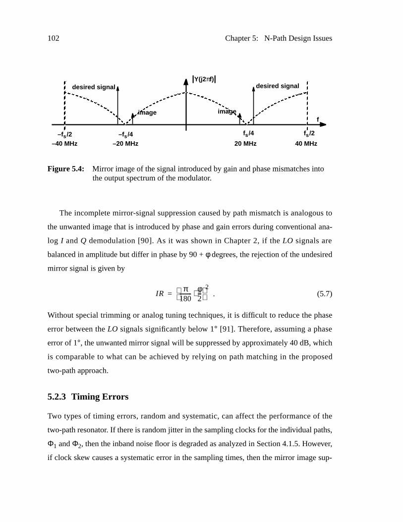
102 Chapter 5: N-Path Design Issues
The incomplete mirror-signal suppression caused by path mismatch is analogous to
the unwanted image that is introduced by phase and gain errors during conventional ana-
log I andQ demodulation [90]. As it was shown in Chapter 2, if theLO signals are
balanced in amplitude but differ in phase by 90 +φdegrees, the rejection of the undesired
mirror signal is given by
. (5.7)
Without special trimming or analog tuning techniques, it is difficult to reduce the phase
error between theLO signals significantly below 1° [91]. Therefore, assuming a phase
error of 1°, the unwanted mirror signal will be suppressed by approximately 40 dB, which
is comparable to what can be achieved by relying on path matching in the proposed
two-path approach.
5.2.3 Timing Err ors
Two types of timing errors, random and systematic, can affect the performance of the
two-path resonator. If there is random jitter in the sampling clocks for the individual paths,
Φ1 andΦ2, then the inband noise floor is degraded as analyzed in Section4.1.5. However,
if clock skew causes a systematic error in the sampling times, then the mirror image sup-
Figure 5.4: Mirror image of the signal introduced by gain and phase mismatches intothe output spectrum of the modulator.
fs /2fs /4–fs /4–fs /220 MHz 40 MHz–40 MHz –20 MHz
|Y(j2πf)|desired signal
image
desired signal
imagef
IRπ
180--------- φ
2---⋅
2=
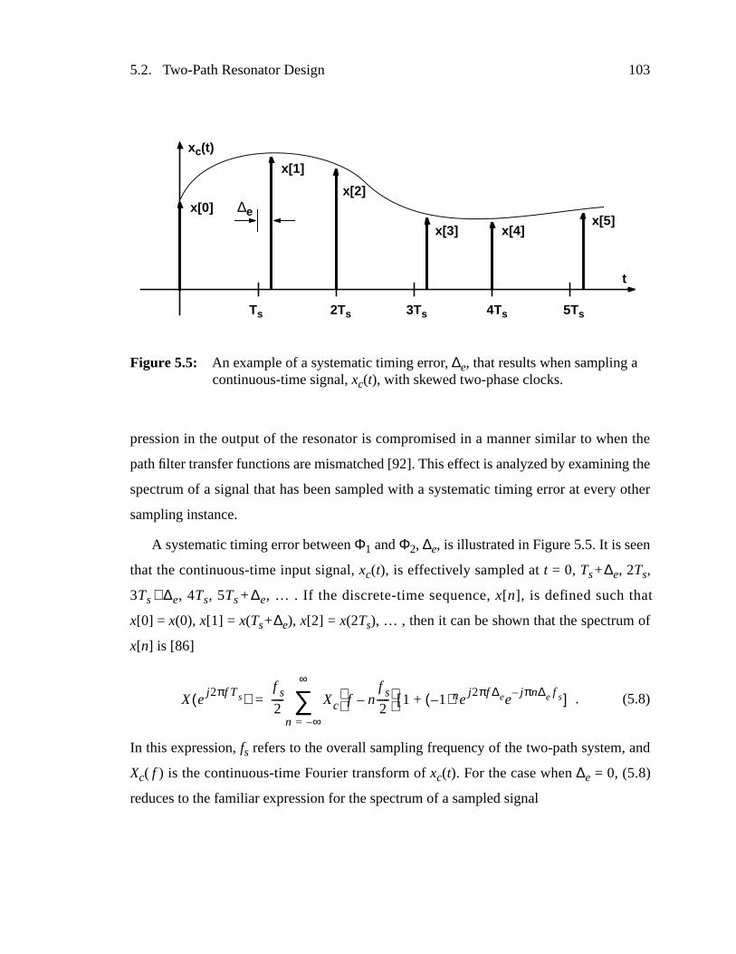
5.2. Two-Path Resonator Design 103
pression in the output of the resonator is compromised in a manner similar to when the
path filter transfer functions are mismatched [92]. This effect is analyzed by examining the
spectrum of a signal that has been sampled with a systematic timing error at every other
sampling instance.
A systematic timing error betweenΦ1 andΦ2, ∆e, is illustrated in Figure5.5. It is seen
that the continuous-time input signal,xc(t), is effectively sampled att = 0, Ts+∆e, 2Ts,
3Ts+∆e, 4Ts, 5Ts+ ∆e, … . If the discrete-time sequence,x[n], is defined such that
x[0] = x(0), x[1] = x(Ts+∆e), x[2] = x(2Ts), … , then it can be shown that the spectrum of
x[n] is [86]
. (5.8)
In this expression,fs refers to the overall sampling frequency of the two-path system, and
Xc( f ) is the continuous-time Fourier transform ofxc(t). For the case when∆e = 0, (5.8)
reduces to the familiar expression for the spectrum of a sampled signal
Figure 5.5: An example of a systematic timing error, ∆e, that results when sampling acontinuous-time signal,xc(t), with skewed two-phase clocks.
Ts 2Ts 3Ts 4Ts 5Ts
x[0]
x[1]
x[2]
x[3] x[4]x[5]
xc(t)
t
∆e
X ej2πf Ts( )
f s
2----- Xc f n
f s
2-----–
1 1–( )nej2πf ∆ee
jπn∆e f s–+[ ]
n ∞–=
∞
∑=
104 Chapter 5: N-Path Design Issues
. (5.9)
Since (5.8) is the spectrum of a sampled signal, it is periodic with respect tofs. There-
fore, assuming thatxc(t) is bandlimited tofs/2, the spectral content between –fs/2 andfs/2
is completely defined by then = 0, 1, and –1 terms in (5.8). The desired signal is then = 0
term, which is
, (5.10)
and the mirror-image responses are then = ±1 terms,
(5.11)
From (5.10) and (5.11) it can be determined that if the input signal,xc(t), is a
unity-amplitude sinusoid with frequency fx, then the output spectrum consists of the
desired component atfx and a mirror image atfs/2 – fx. This is illustrated in Figure5.6.
The timing-related image-rejection ratio,IR∆e, is defined as the ratio of the signal power at
fx to the image power atfs/2 – fx:
(5.12)
If the input signal frequency, fx, is approximatelyfs/4 and∆e << 1/fs, then (5.12) simplifies
to
. (5.13)
X ej2πf Ts( ) f s Xc f nf s–( )
n ∞–=
∞
∑=
Xsig f( ) f sXc f( )=
Xim f( )f s
2-----Xc f
f s
2-----–
1 ej2πf ∆ee
jπ∆e f s––[ ] +=
f s
2-----Xc f
f s
2-----+
1 ej2πf ∆ee
jπ∆e f s–[ ] .
4
1 ej2π f s 2 f x–⁄( )∆ee
jπ∆e f s––
2----------------------------------------------------------------------------=
I R∆e
Psig
Pim----------
2 f s2 4⁄( )×
2 f s2 16⁄( ) 1 e
j2π f s 2 f x–⁄( )∆eejπ∆e f s–
–2××
-----------------------------------------------------------------------------------------------------------------= =
.
I R∆e16
π2∆e2 f s
2-------------------≈
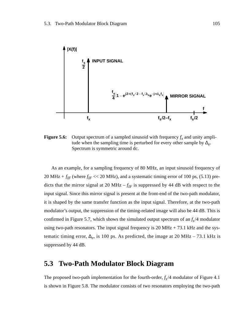
5.3. Two-Path Modulator Block Diagram 105
As an example, for a sampling frequency of 80 MHz, an input sinusoid frequency of
20MHz + fIF (wherefIF << 20 MHz), and a systematic timing error of 100 ps, (5.13) pre-
dicts that the mirror signal at 20 MHz –fIF is suppressed by 44 dB with respect to the
input signal. Since this mirror signal is present at the front-end of the two-path modulator,
it is shaped by the same transfer function as the input signal. Therefore, at the two-path
modulator’s output, the suppression of the timing-related image will also be 44 dB. This is
confirmed in Figure5.7, which shows the simulated output spectrum of anfs/4 modulator
using two-path resonators. The input signal frequency is 20MHz + 73.1kHz and the sys-
tematic timing error, ∆e, is 100 ps. As predicted, the image at 20MHz – 73.1kHz is
suppressed by 44dB.
5.3 Two-Path Modulator Block Diagram
The proposed two-path implementation for the fourth-order, fs/4 modulator of Figure4.1
is shown in Figure5.8. The modulator consists of two resonators employing the two-path
Figure 5.6: Output spectrum of a sampled sinusoid with frequency fx and unity ampli-tude when the sampling time is perturbed for every other sample by∆e.Spectrum is symmetric around dc.
INPUT SIGNAL
MIRROR SIGNAL
fx fs /2–fx
|X(f)|
fs /2
fs2----
fs4---- 1 ej 2π fs 2⁄ fx–( )∆ee jπ∆efs––
f
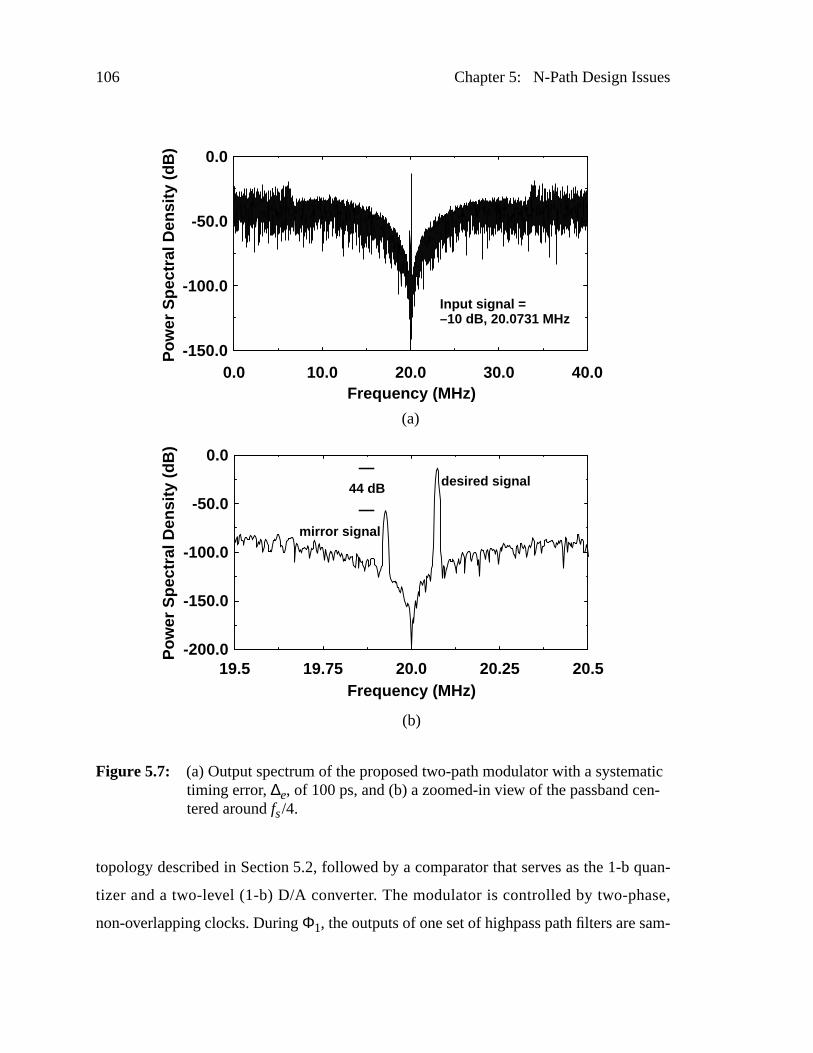
106 Chapter 5: N-Path Design Issues
topology described in Section5.2, followed by a comparator that serves as the 1-b quan-
tizer and a two-level (1-b) D/A converter. The modulator is controlled by two-phase,
non-overlapping clocks. DuringΦ1, the outputs of one set of highpass path filters are sam-
Figure 5.7: (a) Output spectrum of the proposed two-path modulator with a systematictiming error, ∆e, of 100 ps, and (b) a zoomed-in view of the passband cen-tered aroundfs/4.
0.0 10.0 20.0 30.0 40.0-150.0
-100.0
-50.0
0.0
Frequency (MHz)
Pow
er S
pect
ral D
ensi
ty (
dB)
19.5 19.75 20.0 20.25 20.5-200.0
-150.0
-100.0
-50.0
0.0
Frequency (MHz)
Pow
er S
pect
ral D
ensi
ty (
dB)
(a)
(b)
44 dB
Input signal =–10 dB, 20.0731 MHz
desired signal
mirror signal
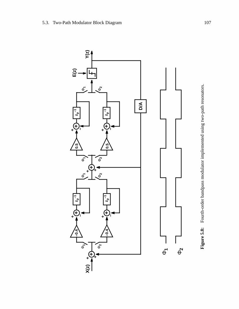
5.3. Two-Path Modulator Block Diagram 107
X(z
)
E(z
)
Y(z
)
0.5
Φ1
Φ2
Φ1
Φ2
Φ1
Φ2
Φ1
Φ2
0.5
z p–1
z p–1
–0.4
–0.4
z p–1
z p–1
D/A
+ ++
+ –+
+ ++
+ –+
+ –+
+ –+
Φ1
Φ2 F
igur
e5.
8:Fo
urth
-ord
er b
andp
ass
mod
ulat
or im
plem
ente
d us
ing
two-
path
res
onat
ors.
108 Chapter 5: N-Path Design Issues
pled, while onΦ2, the outputs of their counterparts are sampled. The quantizer is clocked
on bothΦ1 andΦ2; thus, the sampling rate for the overall modulator is twice that of each
path filter.
5.3.1 Two Interleaved Highpass Modulators
In a switched-capacitor implementation of the proposed two-path modulator, the summa-
tion of the resonator input signal with the quantizer feedback can be merged into the
constituent path filters of each resonator. Upon redrawing the block diagram to reflect this
fact, Figure5.9 shows that the experimental bandpass modulator is essentially comprised
of two independent, interleaved highpass modulators that are clocked 180° out of phase
with each other. Also, in Figure5.9 the single 1-b quantizer in Figure5.8 has been parti-
tioned into two independent 1-b quantizers. It is important to note that the total
quantization noise power in the modulator of Figure5.9 is not doubled by the presence of
two quantizers because the quantizers are clocked on alternate clock cycles and the out-
puts of the two paths are interleaved, not summed.
If the two quantizers are identical, then the output from the modulator in Figure5.9 is
identical to the case where only a single quantizer is used. Although it is not necessary to
partition the quantizer in this manner, the use of separate quantizers allows for a more
modular design and simpler layout. Two independent quantizers were used in the experi-
mental prototype.
Offsets in the comparators can potentially generate out-of-band tones in the output
spectrum. If the offsets in the comparators of Figure5.9 are identical, then the effect is
equivalent to having a dc offset in the comparator of a single-path modulator. In this case,
as explained in Section4.1.4, dc tones can be generated in the output spectrum of the
modulator. If the offsets in the two comparators are mismatched, then tones can be gener-
ated atfs/2 as well as dc. This effect is illustrated in Figure5.10 for the case when one
comparator has an offset of∆/40, and the other comparator has an offset of –∆/40;∆ is the
step size of the two-level quantizer. Intuitively, the presence of a tone atfs/2 is understood
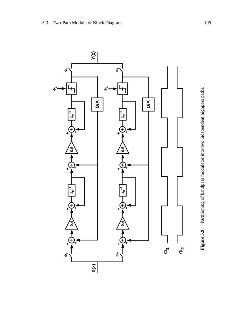
5.3. Two-Path Modulator Block Diagram 109
Fig
ure
5.9:
Part
ition
ing
of b
andp
ass
mod
ulat
or in
to two
inde
pend
ent h
ighp
ass
path
s.
Φ1
X(z
)
Φ2
Φ1
Φ2
Φ1
Φ2
Y(z
)
Φ1
Φ2
0.5
z p–1
z p–1
0.5
–0.4
z p–1
–0.4
z p–1
D/A
D/A
+ –++ ++
+ +++ –+
+ ++
+ ++
+ –+
+ –+
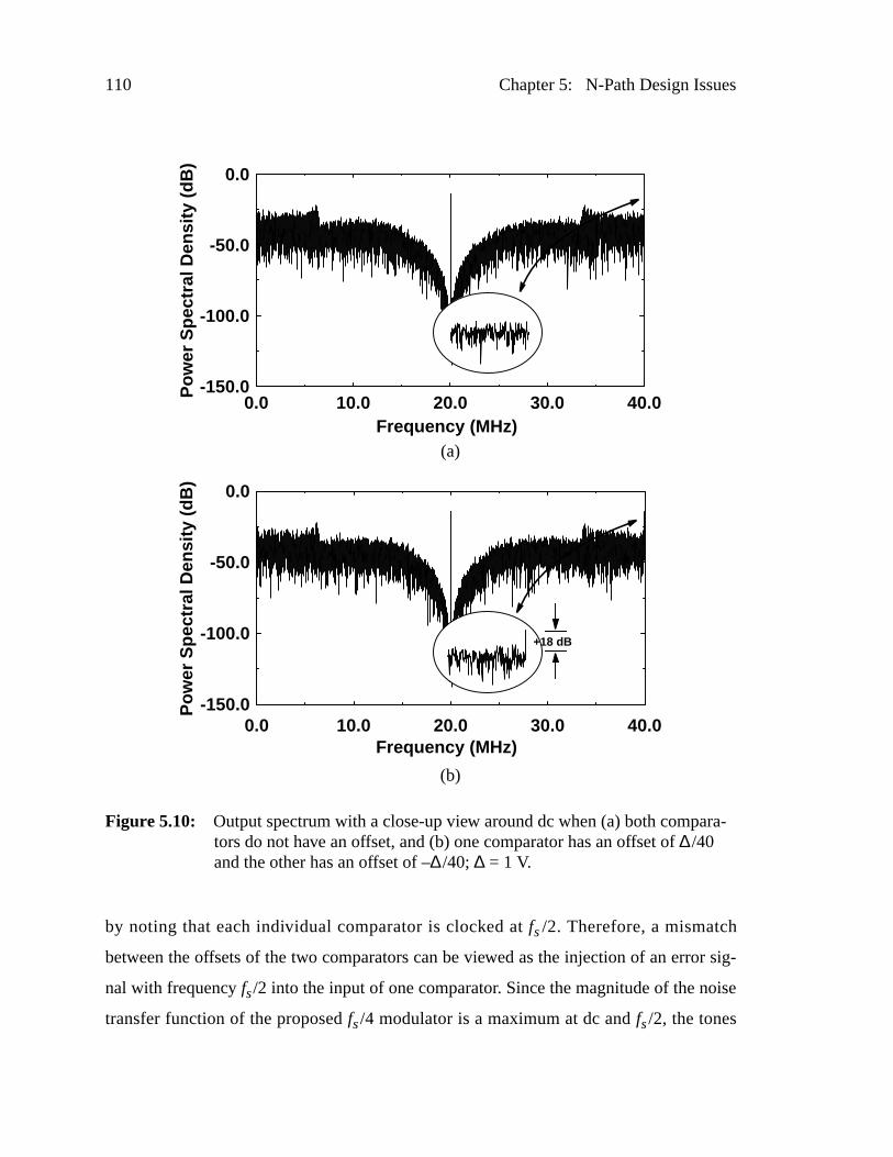
110 Chapter 5: N-Path Design Issues
by noting that each individual comparator is clocked atfs/2. Therefore, a mismatch
between the offsets of the two comparators can be viewed as the injection of an error sig-
nal with frequency fs/2 into the input of one comparator. Since the magnitude of the noise
transfer function of the proposed fs/4 modulator is a maximum at dc andfs/2, the tones
Figure 5.10: Output spectrum with a close-up view around dc when (a) both compara-tors do not have an offset, and (b) one comparator has an offset of∆/40and the other has an offset of –∆/40;∆ = 1 V.
0.0 10.0 20.0 30.0 40.0-150.0
-100.0
-50.0
0.0
0.0 10.0 20.0 30.0 40.0-150.0
-100.0
-50.0
0.0
Frequency (MHz)
Pow
er S
pect
ral D
ensi
ty (
dB)
+18 dB
Frequency (MHz)
Pow
er S
pect
ral D
ensi
ty (
dB)
(a)
(b)
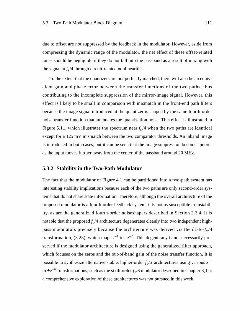
5.3. Two-Path Modulator Block Diagram 111
due to offset are not suppressed by the feedback in the modulator. However, aside from
compressing the dynamic range of the modulator, the net effect of these offset-related
tones should be negligible if they do not fall into the passband as a result of mixing with
the signal atfs/4 through circuit-related nonlinearities.
To the extent that the quantizers are not perfectly matched, there will also be an equiv-
alent gain and phase error between the transfer functions of the two paths, thus
contributing to the incomplete suppression of the mirror-image signal. However, this
effect is likely to be small in comparison with mismatch in the front-end path filters
because the image signal introduced at the quantizer is shaped by the same fourth-order
noise transfer function that attenuates the quantization noise. This effect is illustrated in
Figure5.11, which illustrates the spectrum nearfs/4 when the two paths are identical
except for a 125mV mismatch between the two comparator thresholds. An inband image
is introduced in both cases, but it can be seen that the image suppression becomes poorer
as the input moves further away from the center of the passband around 20 MHz.
5.3.2 Stability in the Two-Path Modulator
The fact that the modulator of Figure4.1 can be partitioned into a two-path system has
interesting stability implications because each of the two paths are only second-order sys-
tems that do not share state information. Therefore, although the overall architecture of the
proposed modulator is a fourth-order feedback system, it is not as susceptible to instabil-
ity, as are the generalized fourth-order noiseshapers described in Section3.3.4. It is
notable that the proposedfs/4 architecture degenerates cleanly into two independent high-
pass modulators precisely because the architecture was derived via the dc-to-fs/4
transformation, (3.23), which mapsz–1 to –z–2. This degeneracy is not necessarily pre-
served if the modulator architecture is designed using the generalized filter approach,
which focuses on the zeros and the out-of-band gain of the noise transfer function. It is
possible to synthesize alternative stable, higher-orderfs/X architectures using variousz–1
to ±z–N transformations, such as the sixth-orderfs/6 modulator described in Chapter 8, but
a comprehensive exploration of these architectures was not pursued in this work.
112 Chapter 5: N-Path Design Issues
Although the two-pathfs/4 modulator has the dynamic behavior of a second-order sys-
tem, it cannot be claimed that it is inherently stable simply because its architecture is
derived from a stable, second-order lowpass modulator. The stability of the two-pathfs/4
modulator is sensitive to specific implementation issues in a manner that is not reflected in
19.5 19.75 20.0 20.25 20.5-150.0
-100.0
-50.0
0.0
Frequency (MHz)
Pow
er S
pect
ral D
ensi
ty (
dB)
84 dB
desired signal
mirror image
fx = 20.053 MHz
19.5 19.75 20.0 20.25 20.5-150.0
-100.0
-50.0
0.0
Frequency (MHz)
Pow
er S
pect
ral D
ensi
ty (
dB)
71 dB
desired signal
mirror image
fx = 20.133 MHz
(a)
(b)
Figure 5.11: Inband image that is introduced by comparator mismatch in the two-pathmodulator for input signal frequencies, (a)fx = 20.053MHz, and(b) fx = 20.133MHz.
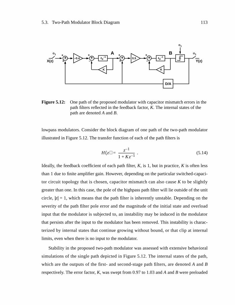
5.3. Two-Path Modulator Block Diagram 113
lowpass modulators. Consider the block diagram of one path of the two-path modulator
illustrated in Figure5.12. The transfer function of each of the path filters is
. (5.14)
Ideally, the feedback coefficient of each path filter, K, is 1, but in practice,K is often less
than 1 due to finite amplifier gain. However, depending on the particular switched-capaci-
tor circuit topology that is chosen, capacitor mismatch can also causeK to be slightly
greater than one. In this case, the pole of the highpass path filter will lie outside of the unit
circle, |z| = 1, which means that the path filter is inherently unstable. Depending on the
severity of the path filter pole error and the magnitude of the initial state and overload
input that the modulator is subjected to, an instability may be induced in the modulator
that persists after the input to the modulator has been removed. This instability is charac-
terized by internal states that continue growing without bound, or that clip at internal
limits, even when there is no input to the modulator.
Stability in the proposed two-path modulator was assessed with extensive behavioral
simulations of the single path depicted in Figure5.12. The internal states of the path,
which are the outputs of the first- and second-stage path filters, are denotedA andB
respectively. The error factor, K, was swept from 0.97 to 1.03 andA andB were preloaded
Figure 5.12: One path of the proposed modulator with capacitor mismatch errors in thepath filters reflected in the feedback factor, K. The internal states of thepath are denotedA andB.
Φ1
X(z)
Φ1 Φ1
Y(z)0.5 zp
–1–0.4 zp–1
D/A
+
–+
+
++
+
++
+
–+
K K
A B
H z( ) z 1–
1 Kz 1–+---------------------=
114 Chapter 5: N-Path Design Issues
with different overload conditions. For the case whenK = 1.01 andA andB are preloaded
to 5 × |Vref /2|, where |Vref /2| is the magnitude of the feedback reference levels, it can be
seen in Figure5.13(a) that the modulator is stable because the internal states subside after
an initial transient period; the inband SNR is also consistent with that predicted by linear
analysis. However, for the case depicted in Figure5.13(b), whenK = 1.02 andA andB are
again preloaded to 5× |Vref/2|, the modulator is clearly unstable; the states continue grow-
ing until they are artificially clipped in the simulation. The relationship between capacitor
mismatch in the switched-capacitor circuit and the error feedback factor, K, in the block
diagram is determined by the specific circuit topology chosen and will be discussed in the
following chapter.
5.4 Summary
In this chapter, the essential relationships forN-path filters were reviewed, and it was
shown that the resonators of the proposed, fourth-order, fs/4 modulator can be imple-
mented easily by interleaving two highpass filters. The nonidealities of the two-path
resonator were explored within the context of the bandpass modulator. It is seen that path
mismatch leads to an image of the desired signal produced at a mirror frequency centered
aroundfs/4. This is analogous to the image that is produced by phase and gain errors dur-
ing analogI andQ demodulation. Systematic timing errors that result in nonuniform
sampling of the input signal also result in incomplete image suppression.
It was also shown that it is possible to partition the modulator into two independent
second-order paths. The stability of the modulator is then seen to be governed by sec-
ond-order dynamics. However, if the path filters that comprise the modulator are unstable
because of implementation nonidealities, it is possible to excite the modulator into an
unstable state that is characterized by large oscillations in internal states and a poor inband
SNR that is not commensurate with that predicted by linear analysis. The potential for the
onset of instability is related to the initial conditions in the modulator as well as the magni-
tude of the error resulting from circuit nonidealities such as capacitor mismatch.
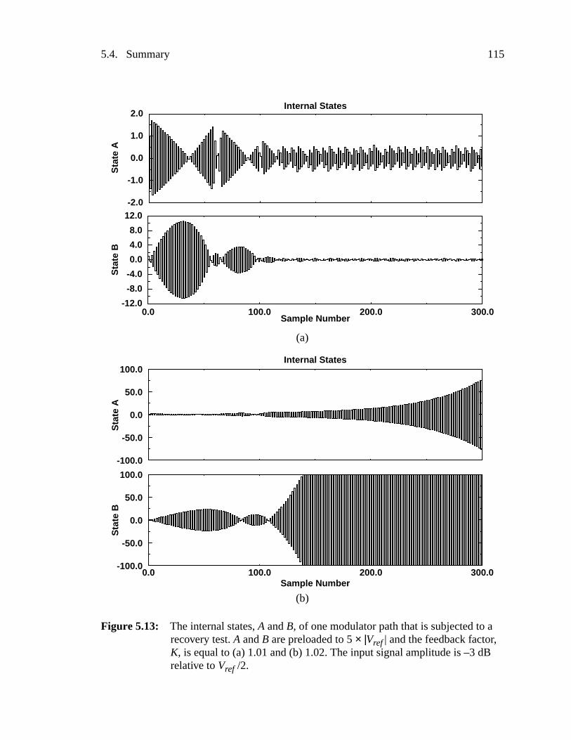
5.4. Summary 115
Figure 5.13: The internal states,A andB, of one modulator path that is subjected to arecovery test.A andB are preloaded to 5× |Vref| and the feedback factor,K, is equal to (a) 1.01 and (b) 1.02. The input signal amplitude is –3 dBrelative toVref /2.
-100.0
-50.0
0.0
50.0
100.0
-2.0
-1.0
0.0
1.0
2.0
0.0 100.0 200.0 300.0-12.0
-8.0
-4.0
0.0
4.0
8.0
12.0
Internal States
Sample Number
Sta
te A
Sta
te B
0.0 100.0 200.0 300.0-100.0
-50.0
0.0
50.0
100.0
Sta
te A
Sta
te B
Internal States
Sample Number
(a)
(b)

116 Chapter 5: N-Path Design Issues
Fortunately, behavioral simulations indicate that the modulator remains stable for a wide
range of overload conditions provided that the pole error in the path filters remains
bounded by approximately 1%. In the following chapter, it is shown that this condition
requires capacitor matching on the order of 1% (which can readily be achieved) for the
specific circuit topology chosen to implement the path filter.
117
Chapter
6 Implementation
This chapter describes the design and implementation of anfs/4 bandpass modulator that
utilizes the two-path architecture proposed in Chapter 5. The objective of this design is to
demonstrate the feasibility of implementing a modulator with an effective sampling fre-
quency as high as 80 MHz and a dynamic range exceeding 70 dB for a 200-kHz passband
centered atfs/4. For this oversampling ratio, the fourth-order architecture is designed to
suppress inband quantization noise by a large margin with respect to the noise floor set by
electronic noise.
The experimental modulator has been integrated in a 0.6-µm, single-poly, triple-metal
CMOS technology. This technology does not include a high-density, linear capacitor
option such as double-poly or poly-diffusion capacitors. Therefore, the capacitors were
implemented using the capacitance between metal interconnect layers. This results in a
substantial power dissipation penalty because of the large parasitics associated with the
capacitor structures. For this reason, power dissipation in the prototype was only loosely
constrained to be less than 100 mW when the modulator is operated from a 3.3-V supply.
Substantial power savings should be possible in a technology with a smaller bottom-plate
parasitic capacitance.
6.1 Switched-Capacitor Highpass Path Filter
As described in Section5.3, the proposed two-path modulator is comprised offs/4 resona-
tors that are implemented using two interleaved highpass filters, each with the path trans-
fer function
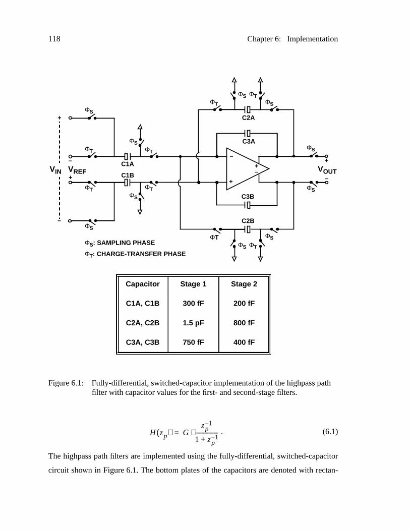
118 Chapter 6: Implementation
. (6.1)
The highpass path filters are implemented using the fully-differential, switched-capacitor
circuit shown in Figure6.1. The bottom plates of the capacitors are denoted with rectan-
H zp( ) Gzp
1–
1 zp1–+
-----------------⋅=
ΦS
ΦS
ΦT
ΦT
C1A
ΦS
ΦS
ΦS
ΦS
ΦT
ΦT
C1B+–
+
–
VIN
ΦT
ΦTΦSΦS
C2A
C3A
ΦTΦTΦS
ΦS
C2B
C3B
+
VOUT
+
–+
–VREF
–
ΦS: SAMPLING PHASE
ΦT: CHARGE-TRANSFER PHASE
Figure6.1: Fully-differential, switched-capacitor implementation of the highpass pathfilter with capacitor values for the first- and second-stage filters.
Capacitor Stage 1 Stage 2
C1A, C1B 300 fF 200 fF
C2A, C2B 1.5 pF 800 fF
C3A, C3B 750 fF 400 fF
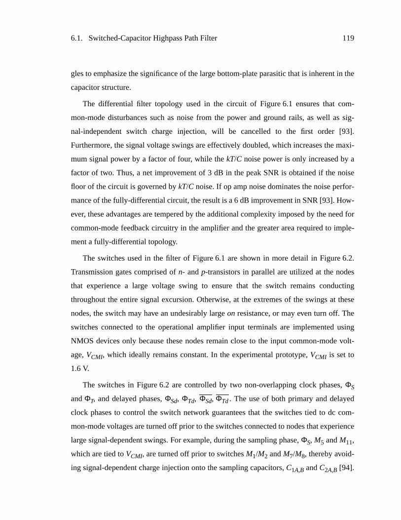
6.1. Switched-Capacitor Highpass Path Filter 119
gles to emphasize the significance of the large bottom-plate parasitic that is inherent in the
capacitor structure.
The differential filter topology used in the circuit of Figure6.1 ensures that com-
mon-mode disturbances such as noise from the power and ground rails, as well as sig-
nal-independent switch charge injection, will be cancelled to the first order [93].
Furthermore, the signal voltage swings are effectively doubled, which increases the maxi-
mum signal power by a factor of four, while thekT/C noise power is only increased by a
factor of two. Thus, a net improvement of 3 dB in the peak SNR is obtained if the noise
floor of the circuit is governed bykT/C noise. If op amp noise dominates the noise perfor-
mance of the fully-differential circuit, the result is a 6 dB improvement in SNR [93]. How-
ever, these advantages are tempered by the additional complexity imposed by the need for
common-mode feedback circuitry in the amplifier and the greater area required to imple-
ment a fully-differential topology.
The switches used in the filter of Figure6.1 are shown in more detail in Figure6.2.
Transmission gates comprised ofn- andp-transistors in parallel are utilized at the nodes
that experience a large voltage swing to ensure that the switch remains conducting
throughout the entire signal excursion. Otherwise, at the extremes of the swings at these
nodes, the switch may have an undesirably largeon resistance, or may even turn off. The
switches connected to the operational amplifier input terminals are implemented using
NMOS devices only because these nodes remain close to the input common-mode volt-
age,VCMI, which ideally remains constant. In the experimental prototype,VCMI is set to
1.6V.
The switches in Figure6.2 are controlled by two non-overlapping clock phases,ΦS
andΦT, and delayed phases,ΦSd, ΦTd, . The use of both primary and delayed
clock phases to control the switch network guarantees that the switches tied to dc com-
mon-mode voltages are turned off prior to the switches connected to nodes that experience
large signal-dependent swings. For example, during the sampling phase,ΦS, M5 andM11,
which are tied toVCMI, are turned off prior to switchesM1/M2 andM7/M8, thereby avoid-
ing signal-dependent charge injection onto the sampling capacitors,C1A,B andC2A,B [94].
ΦSd, ΦTd
120 Chapter 6: Implementation
Figure6.2: Switch networks used to sample the (a) input signal and (b) output of theamplifier in the highpass path filter. Transistor sizes are inµm.
ΦS
C1A +–
+
–
M1
M2
M3 M4 M5
M6
ΦSd
ΦSd
ΦTd
ΦT
ΦTd
–VREF/2
VIN /2
VCMI=1.6V
+–
+
–
ΦS
C2AM7
M8
M9M10M11
M12
ΦSd
ΦSd
ΦTd
ΦT
ΦTd
(a)
(b)
24/0.6
24/0.6 12/0.6
12/0.624/0.6
24/0.6
60/0.6
60/0.660/0.6
60/0.6
45/0.6
60/0.6
VCMI=1.6VVCMI=1.6V
6.1. Switched-Capacitor Highpass Path Filter 121
Similarly, during the charge-transfer phase,ΦT, the switches connected to the op amp
input terminals,M6 andM12, are turned off before switchesM3/M4 andM9/M10 to insure
that the charge injected onto the integration capacitors,C3A,B, is, to first order, indepen-
dent of the signal.
6.1.1 Filter Operation
The filter operation during the sampling and charge-transfer phases is depicted in
Figure6.3. On the sampling phase,ΦS, a charge proportional toVIN is stored onC1A and
C1B, and a charge proportional toVOUT is stored acrossC2A and C2B. On the subsequent
charge-redistribution phase,ΦT, –VREF is sampled ontoC1A,B, and charge is transferred
from C1A to C3A, C1B to C3B, C2A to C3B, andC2B to C3A. Because the capacitorsC2A and
C2B are cross-coupled around the operational amplifier, the charge transferred fromC2A
andC2B effectively undergoes an inversion during the charge-redistribution phase. In the
z-domain, the output of the highpass path filter is thus
(6.2)
where, as explained in Section5.1, zp–1 denotes a single delay with respect to the path
sampling frequency. WhenC2B,A = 2 × C3A,B, the path filter realizes the desired highpass
transfer function of (6.1).
The sampling and charge-transfer phases of the path filter can be related to the opera-
tion of the proposed, two-path bandpass modulator by referring to the timing diagram
depicted in Figure5.9. It is seen that theΦ1 path, which can be regarded as one of two
independent parallel modulators with interleaved outputs, samples the input,X(z), on
phaseΦ1 and redistributes charge on phaseΦ2, whereas theΦ2 path operates 180° degrees
out of phase with theΦ1 path, sampling the input on phaseΦ2 and redistributing charge on
phaseΦ1.
VOUT zp( )C1A
C3A----------
zp1–
1C2B
C3A---------- 1–
zp1–
+
------------------------------------------ VIN zp( ) VREF zp( )+( )××=
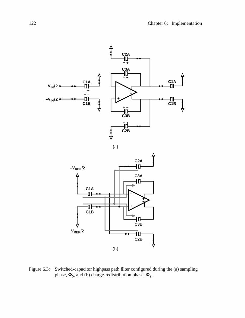
122 Chapter 6: Implementation
C3A
C2A
+–
+
–C1A
C3B
C1B
C2B
C3A
C2A
+–
+
–C1A
C1B
VIN/2
–VIN/2
C1A
C1B
C3B
C2B
(a)
(b)
–VREF/2
VREF/2
Figure6.3: Switched-capacitor highpass path filter configured during the (a) samplingphase,ΦS, and (b) charge-redistribution phase, ΦT.
+ –+ –
+ –
+ –
+ –
+ –
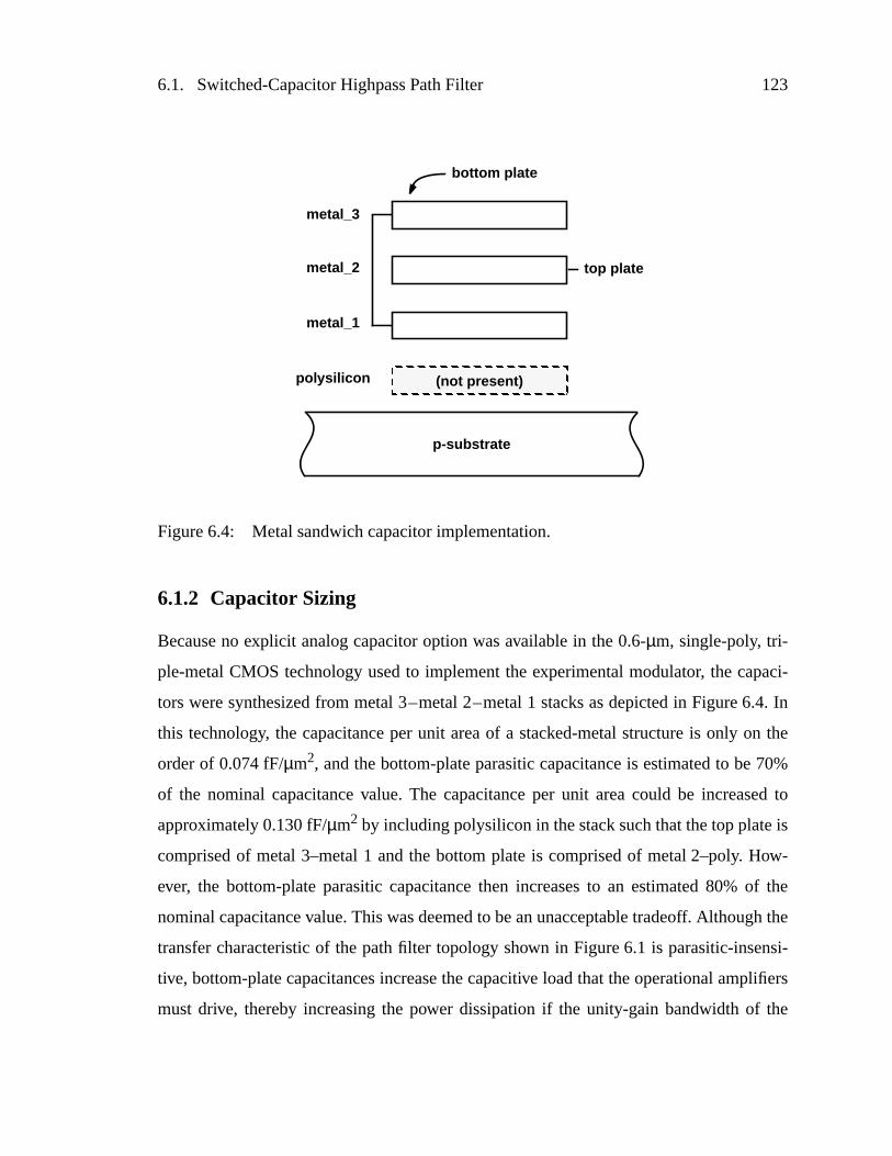
6.1. Switched-Capacitor Highpass Path Filter 123
6.1.2 Capacitor Sizing
Because no explicit analog capacitor option was available in the 0.6-µm, single-poly, tri-
ple-metal CMOS technology used to implement the experimental modulator, the capaci-
tors were synthesized from metal 3–metal 2–metal 1 stacks as depicted in Figure6.4. In
this technology, the capacitance per unit area of a stacked-metal structure is only on the
order of 0.074fF/µm2, and the bottom-plate parasitic capacitance is estimated to be 70%
of the nominal capacitance value. The capacitance per unit area could be increased to
approximately 0.130 fF/µm2 by including polysilicon in the stack such that the top plate is
comprised of metal 3–metal 1 and the bottom plate is comprised of metal2–poly. How-
ever, the bottom-plate parasitic capacitance then increases to an estimated 80% of the
nominal capacitance value. This was deemed to be an unacceptable tradeoff. Although the
transfer characteristic of the path filter topology shown in Figure6.1 is parasitic-insensi-
tive, bottom-plate capacitances increase the capacitive load that the operational amplifiers
must drive, thereby increasing the power dissipation if the unity-gain bandwidth of the
Figure6.4: Metal sandwich capacitor implementation.
metal_3
metal_2
metal_1
pol ysilicon
p-substrate
top plate
bottom plate
(not present)
124 Chapter 6: Implementation
amplifier is to remain constant. In this technology, it is imperative to keep the size of the
capacitors as small as allowed bykT/C noise and matching considerations.
With the preceding considerations in mind, the input sampling capacitors in the first
stage,C1A,B, were sized at 300 fF. The feedback capacitors,C3A,B, are governed by the
desired resonator gain,C1A,B/C3A,B, and the output sampling capacitors,C2A,B, are deter-
mined by (6.2) to be twice the value ofC3A,B. Smaller capacitors can be used in the filters
comprising the second stage of the proposed, two-path modulator because of relaxed
requirements with respect tokT/C noise and capacitor mismatch as compared to the
first-stage filters. Errors introduced after the first stage of the modulator are attenuated by
noiseshaping in addition to oversampling [14]. Thus, sampling capacitors of the second
stage were scaled to 200 fF to reduce the loading on both the first and second-stage opera-
tional amplifiers.
6.1.3 Switch Noise
Two noise sources intrinsic to the MOS switches, thermal noise and flicker noise, can
potentially perturb the filter operation. Thermal noise is associated with the random
motion of carriers in the resistive channel, and flicker (1/f ) noise is associated with flow of
direct current in the device. In the analysis of switch noise below, 1/f noise is considered
negligible because it is assumed there is no static current flowing through the switched
capacitors, and hence, none through the MOS device [95].
The thermal noise contributed by the MOS switches in the path filter can be estimated
by modeling each switch path with the sample-and-hold circuit shown in Figure6.5.
WhenΦS is high and the MOS switch is on, the channel is modeled as a noiseless resistor,
RON, in series with a noise source,eR, that has a power spectral density
(6.3)
wherek is Boltzmann’s constant andT is absolute temperature. The variance of the noise
sampled onto capacitorCS is determined by integrating the noise power spectral density,
SR f( ) 4kTRON ,= 0 f ∞< <
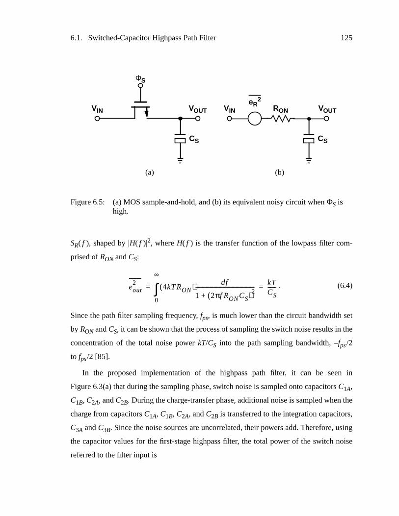
6.1. Switched-Capacitor Highpass Path Filter 125
SR( f ), shaped by |H( f )|2, whereH( f ) is the transfer function of the lowpass filter com-
prised ofRON andCS:
. (6.4)
Since the path filter sampling frequency, fps, is much lower than the circuit bandwidth set
by RON andCS, it can be shown that the process of sampling the switch noise results in the
concentration of the total noise power kT/CS into the path sampling bandwidth, –fps/2
to fps/2 [85].
In the proposed implementation of the highpass path filter, it can be seen in
Figure6.3(a) that during the sampling phase, switch noise is sampled onto capacitorsC1A,
C1B, C2A, andC2B. During the charge-transfer phase, additional noise is sampled when the
charge from capacitorsC1A, C1B, C2A, andC2B is transferred to the integration capacitors,
C3A andC3B. Since the noise sources are uncorrelated, their powers add. Therefore, using
the capacitor values for the first-stage highpass filter, the total power of the switch noise
referred to the filter input is
ΦS
CS
VIN VOUT
CS
VIN VOUTeR
2
RON
Figure6.5: (a) MOS sample-and-hold, and (b) its equivalent noisy circuit whenΦS ishigh.
(a) (b)
eout2
4kTRON( ) df
1 2πf RONCS( )2+
---------------------------------------------
0
∞
∫ kTCS------= =
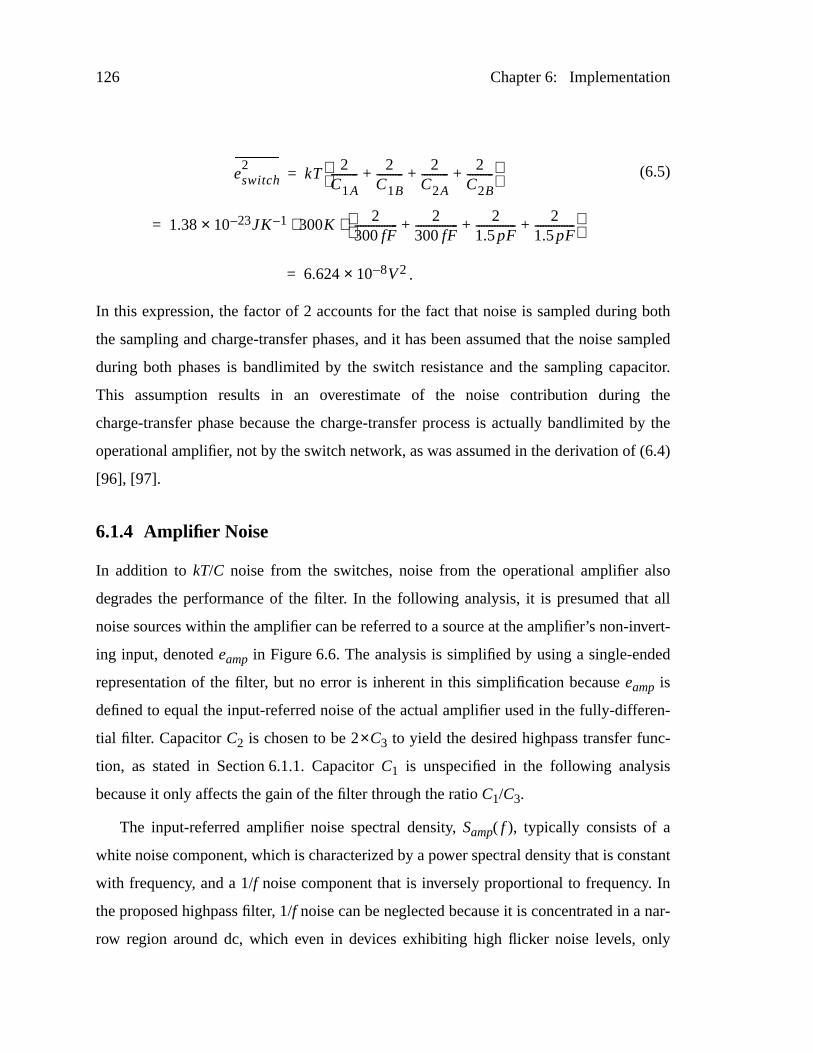
126 Chapter 6: Implementation
(6.5)
In this expression, the factor of 2 accounts for the fact that noise is sampled during both
the sampling and charge-transfer phases, and it has been assumed that the noise sampled
during both phases is bandlimited by the switch resistance and the sampling capacitor.
This assumption results in an overestimate of the noise contribution during the
charge-transfer phase because the charge-transfer process is actually bandlimited by the
operational amplifier, not by the switch network, as was assumed in the derivation of (6.4)
[96], [97].
6.1.4 Amplifier Noise
In addition tokT/C noise from the switches, noise from the operational amplifier also
degrades the performance of the filter. In the following analysis, it is presumed that all
noise sources within the amplifier can be referred to a source at the amplifier’s non-invert-
ing input, denotedeamp in Figure6.6. The analysis is simplified by using a single-ended
representation of the filter, but no error is inherent in this simplification becauseeamp is
defined to equal the input-referred noise of the actual amplifier used in the fully-differen-
tial filter. CapacitorC2 is chosen to be 2×C3 to yield the desired highpass transfer func-
tion, as stated in Section6.1.1. CapacitorC1 is unspecified in the following analysis
because it only affects the gain of the filter through the ratioC1/C3.
The input-referred amplifier noise spectral density, Samp( f ), typically consists of a
white noise component, which is characterized by a power spectral density that is constant
with frequency, and a 1/f noise component that is inversely proportional to frequency. In
the proposed highpass filter, 1/f noise can be neglected because it is concentrated in a nar-
row region around dc, which even in devices exhibiting high flicker noise levels, only
eswi tch2
kT2
C1A---------- 2
C1B---------- 2
C2A---------- 2
C2B----------+ + +
=
1.38 10 23– JK 1–× 300K2
300fF---------------- 2
300fF---------------- 2
1.5pF--------------- 2
1.5pF---------------+ + +
⋅⋅=
6.624 10 8–× V2= .
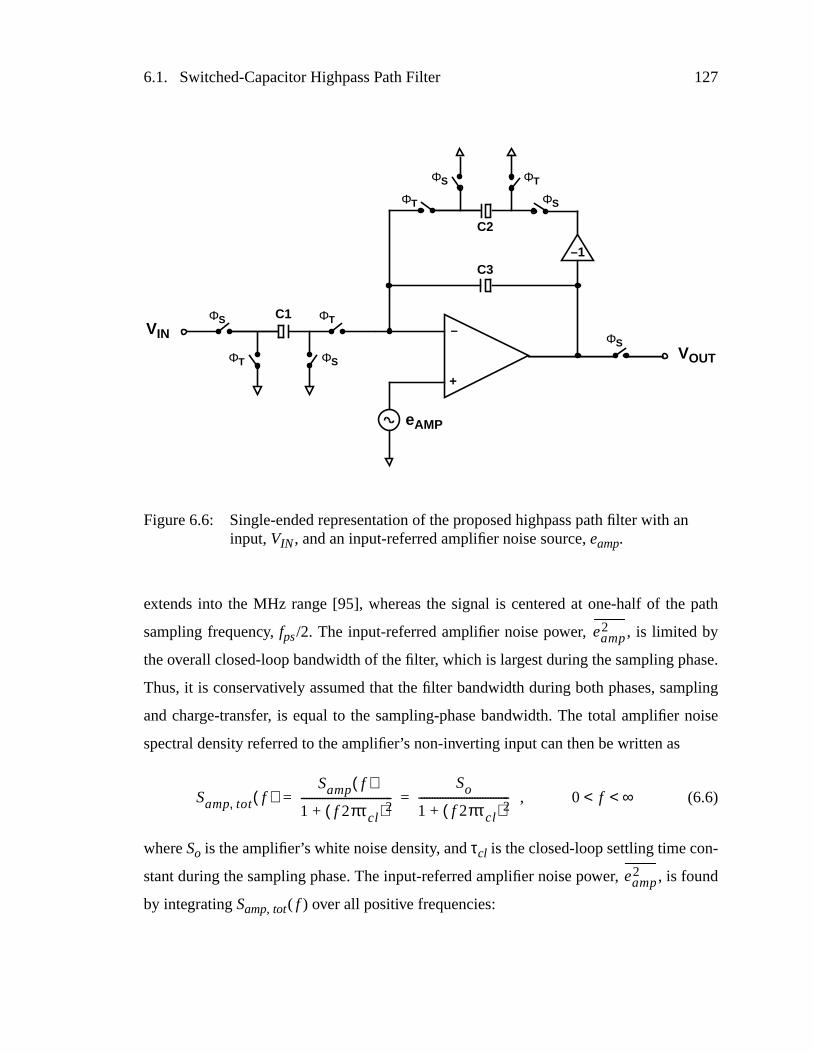
6.1. Switched-Capacitor Highpass Path Filter 127
extends into the MHz range [95], whereas the signal is centered at one-half of the path
sampling frequency, fps/2. The input-referred amplifier noise power, , is limited by
the overall closed-loop bandwidth of the filter, which is largest during the sampling phase.
Thus, it is conservatively assumed that the filter bandwidth during both phases, sampling
and charge-transfer, is equal to the sampling-phase bandwidth. The total amplifier noise
spectral density referred to the amplifier’s non-inverting input can then be written as
(6.6)
whereSo is the amplifier’s white noise density, andτcl is the closed-loop settling time con-
stant during the sampling phase. The input-referred amplifier noise power, , is found
by integratingSamp, tot( f ) over all positive frequencies:
ΦS
+
–
ΦT
ΦTΦS
ΦS
C2
C3
VOUT
ΦT
ΦT ΦS
ΦS C1
–1
VIN
eAMP
Figure6.6: Single-ended representation of the proposed highpass path filter with aninput,VIN, and an input-referred amplifier noise source,eamp.
eamp2
Samp tot, f( )Samp f( )
1 f 2πτcl( )2+----------------------------------
So
1 f 2πτcl( )2+---------------------------------- ,= = 0 f ∞< <
eamp2
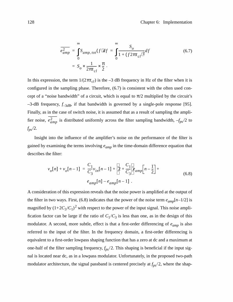
128 Chapter 6: Implementation
(6.7)
In this expression, the term 1/(2πτcl) is the –3 dB frequency in Hz of the filter when it is
configured in the sampling phase. Therefore, (6.7) is consistent with the often used con-
cept of a “noise bandwidth” of a circuit, which is equal toπ/2 multiplied by the circuit’s
–3-dB frequency, f–3dB, if that bandwidth is governed by a single-pole response [95].
Finally, as in the case of switch noise, it is assumed that as a result of sampling the ampli-
fier noise, is distributed uniformly across the filter sampling bandwidth, –fps/2 to
fps/2.
Insight into the influence of the amplifier’s noise on the performance of the filter is
gained by examining the terms involving eamp in the time-domain difference equation that
describes the filter:
(6.8)
A consideration of this expression reveals that the noise power is amplified at the output of
the filter in two ways. First, (6.8) indicates that the power of the noise termeamp[n–1/2] is
magnified by (1+2C3/C1)2 with respect to the power of the input signal. This noise ampli-
fication factor can be large if the ratio ofC1/C3 is less than one, as in the design of this
modulator. A second, more subtle, effect is that a first-order differencing ofeamp is also
referred to the input of the filter. In the frequency domain, a first-order differencing is
equivalent to a first-order lowpass shaping function that has a zero at dc and a maximum at
one-half of the filter sampling frequency, fps/2. This shaping is beneficial if the input sig-
nal is located near dc, as in a lowpass modulator. Unfortunately, in the proposed two-path
modulator architecture, the signal passband is centered precisely atfps/2, where the shap-
eamp2 Samp tot, f( ) fd
0
∞
∫So
1 f 2πτcl( )2+---------------------------------- fd
0
∞
∫= =
So1
2πτcl-------------× π
2---×= .
eamp2
vo n[ ] vo n 1–[ ]+C1
C3------vin n 1–[ ] 2
C1
C3------+
eamp n12---–+ +=
eamp n[ ] eamp n 1–[ ]– .
6.1. Switched-Capacitor Highpass Path Filter 129
ing function applied to the amplifier noise has its maximum amplitude. In other words, the
amplifier noise is shaped to have a maximum spectral density in the desired passband.
The preceding discussion provides a qualitative feel for the noise behavior of the pro-
posed highpass path filter with respect to the amplifier. However, it is difficult to quantita-
tively assess the impact of amplifier noise,eamp, on the performance of the proposed
two-path modulator by only considering the stand-alone filter. For example, it is known
that amplifier noise in a switched-capacitor integrator with sampling capacitanceCS and
integration capacitanceCI experiences a power gain of (1+CI /CS)2 when it is referred to
the input of the integrator [98]. If the integrator gain, CS/CI is small, the noise amplifica-
tion factor can be substantial. However, when the integrator is embedded in the feedback
loop of a lowpassΣ∆ modulator, a substantial fraction of the amplifier noise power experi-
ences lowpass noiseshaping, which suppresses it in the signal band. This effect is not evi-
dent from a consideration of the integrator alone. A more complete description of this
phenomenon in lowpass modulators can be found in [98]. An analogous shaping of the
amplifier noise occurs in the proposed two-pathfs/4 modulator. Unfortunately, this shap-
ing results in a noise gain from the amplifier to the output of the modulator, rather than a
noise suppression as in the lowpass case. A detailed discussion of this effect is deferred
until Section6.3 when the noise of the entire two-path modulator is analyzed.
6.1.5 Filter Stability
A close consideration of (6.2) reveals the disturbing possibility that the highpass path filter
will be unstable if the ratioC2B/C3A is greater than two. In that case, the path filter has a
pole outside the unit circle,|z| = 1, indicating that the impulse response of the filter is
unbounded and may saturate the filter, as well as the modulator, in the manner described in
Section5.3.2. Fortunately, for C2B = 2C3A, extensive behavioral simulations indicate
empirically that the experimental modulator is stable if capacitor matching is good to at
least 1%. With this level of matching, simulations show that the internal states of the mod-
ulator remain bounded under all non-overload conditions. Furthermore, the modulator
recovers from being overdriven at the input, or when initially placed in an overload state.
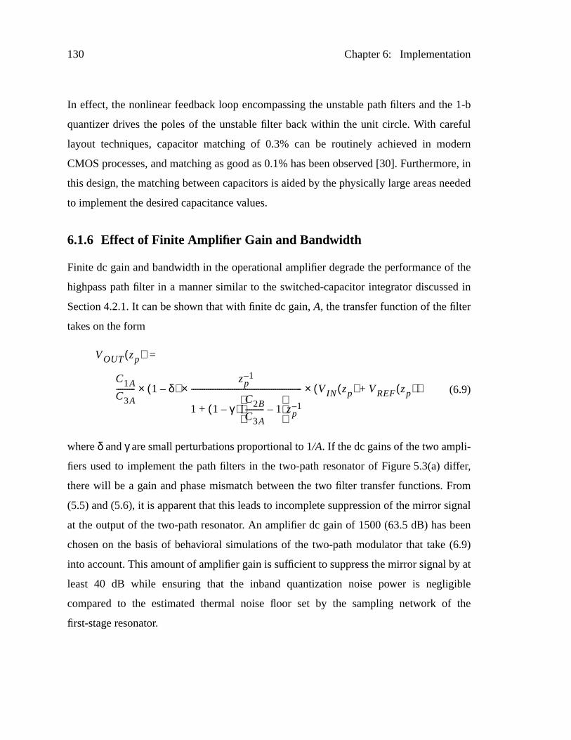
130 Chapter 6: Implementation
In effect, the nonlinear feedback loop encompassing the unstable path filters and the 1-b
quantizer drives the poles of the unstable filter back within the unit circle. With careful
layout techniques, capacitor matching of 0.3% can be routinely achieved in modern
CMOS processes, and matching as good as 0.1% has been observed [30]. Furthermore, in
this design, the matching between capacitors is aided by the physically large areas needed
to implement the desired capacitance values.
6.1.6 Effect of Finite Amplifier Gain and Bandwidth
Finite dc gain and bandwidth in the operational amplifier degrade the performance of the
highpass path filter in a manner similar to the switched-capacitor integrator discussed in
Section4.2.1. It can be shown that with finite dc gain,A, the transfer function of the filter
takes on the form
(6.9)
whereδ andγ are small perturbations proportional to 1/A. If the dc gains of the two ampli-
fiers used to implement the path filters in the two-path resonator of Figure5.3(a) differ,
there will be a gain and phase mismatch between the two filter transfer functions. From
(5.5) and (5.6), it is apparent that this leads to incomplete suppression of the mirror signal
at the output of the two-path resonator. An amplifier dc gain of 1500 (63.5 dB) has been
chosen on the basis of behavioral simulations of the two-path modulator that take (6.9)
into account. This amount of amplifier gain is sufficient to suppress the mirror signal by at
least 40 dB while ensuring that the inband quantization noise power is negligible
compared to the estimated thermal noise floor set by the sampling network of the
first-stage resonator.
C1A
C3A---------- 1 δ–( )
zp1–
1 1 γ–( )C2B
C3A---------- 1–
zp1–+
-----------------------------------------------------------×× VIN zp( ) VREF zp( )+( )×
VOUT zp( ) =
6.2. Circuit Design 131
Under linear settling conditions, incomplete amplifier settling only introduces a gain
error in the highpass filter transfer function, such that
(6.10)
whereε= exp(–T/τ), T is the time available for settling, andτ is the closed-loop settling
time constant. In the two-path resonator of Figure5.3(a), if the two constituent highpass
path filters settle with slightly different time constants,τ1 andτ2, then the mirror signal is
again incompletely suppressed because the gains of the two path filters are mismatched.
Consequently, at least 5τ to 6τ are required for settling so that small variations inτ
between the two filters do not cause a substantial gain mismatch. If the amplifier settling
has a signal-dependent slewing component, then the effects of incomplete settling upon
the two-path resonator cannot be assessed by modeling the highpass path filters with
(6.10) [49], [79]. The amplifiers in the first-stage resonator must, in fact, be designed to
settle to the full precision of the modulator, which requires a closed-loop settling time of
no less than 9τ for a dynamic range of 78 dB. It should be emphasized that distortion due
to amplifier slewing can be a concern even at low input signal levels because the full-scale
differential reference voltages are fed back to the path filters on every cycle, as indicated
by Figure6.1. In the following chapter, incomplete nonlinear settling is identified as the
primary mechanism that limits the performance of the experimental modulator.
6.2 Cir cuit Design
6.2.1 Folded-Cascode Amplifier
With attention toward the requirements for high bandwidth and a modest dc gain of 1500,
the folded-cascode operational amplifier shown in Figure6.7 was used to implement the
switched-capacitor highpass path filters. This topology was chosen over the potentially
faster telescopic-cascode topology because its input and output common-mode levels are
VOUT zp( )C1A
C3A---------- 1 ε–( )×
zp1–
1C2B
C3A---------- 1–
zp1–
+
------------------------------------------× VIN zp( ) VREF zp( )+( )×=
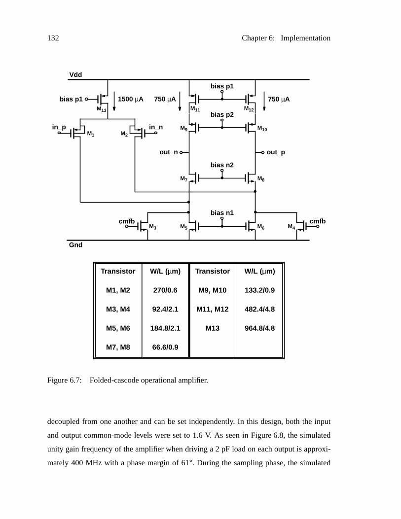
132 Chapter 6: Implementation
decoupled from one another and can be set independently. In this design, both the input
and output common-mode levels were set to 1.6 V. As seen in Figure6.8, the simulated
unity gain frequency of the amplifier when driving a 2 pF load on each output is approxi-
mately 400 MHz with a phase margin of 61°. During the sampling phase, the simulated
bias n2
bias n1
bias p2
bias p1
cmfbcmfb
bias p1
in_p in_n
out_pout_n
Vdd
Gnd
1500 µA 750 µA750 µA
M1 M2
M6M5M3 M4
M9 M10
M8M7
M11 M12M13
Transistor W/L (µm) Transistor W/L (µm)
M1, M2 270/0.6 M9, M10 133.2/0.9
M3, M4 92.4/2.1 M11, M12 482.4/4.8
M5, M6 184.8/2.1 M13 964.8/4.8
M7, M8 66.6/0.9
Figure6.7: Folded-cascode operational amplifier.
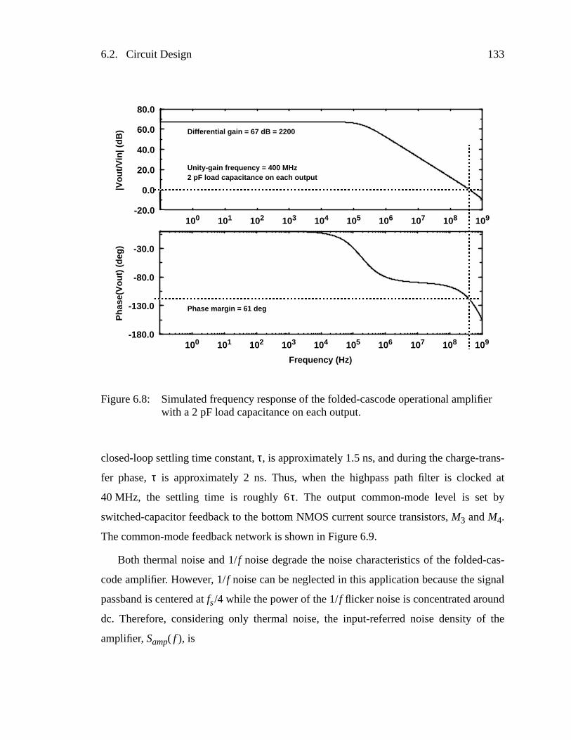
6.2. Circuit Design 133
closed-loop settling time constant,τ, is approximately 1.5 ns, and during the charge-trans-
fer phase,τ is approximately 2 ns. Thus, when the highpass path filter is clocked at
40MHz, the settling time is roughly 6τ. The output common-mode level is set by
switched-capacitor feedback to the bottom NMOS current source transistors,M3 andM4.
The common-mode feedback network is shown in Figure6.9.
Both thermal noise and 1/f noise degrade the noise characteristics of the folded-cas-
code amplifier. However, 1/f noise can be neglected in this application because the signal
passband is centered atfs/4 while the power of the 1/f flicker noise is concentrated around
dc. Therefore, considering only thermal noise, the input-referred noise density of the
amplifier, Samp( f ), is
Figure6.8: Simulated frequency response of the folded-cascode operational amplifierwith a 2 pF load capacitance on each output.
100 101 102 103 104 105 106 107 108 109-20.0
0.0
20.0
40.0
60.0
80.0
100 101 102 103 104 105 106 107 108 109-180.0
-130.0
-80.0
-30.0
|Vou
t/Vin
| (dB
)P
hase
(Vou
t) (
deg)
Differential gain = 67 dB = 2200
Phase margin = 61 deg
2 pF load capacitance on each outputUnity-gain frequency = 400 MHz
Frequency (Hz)
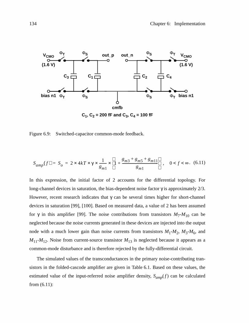
134 Chapter 6: Implementation
. (6.11)
In this expression, the initial factor of 2 accounts for the differential topology. For
long-channel devices in saturation, the bias-dependent noise factorγ is approximately 2/3.
However, recent research indicates thatγ can be several times higher for short-channel
devices in saturation [99], [100]. Based on measured data, a value of 2 has been assumed
for γ in this amplifier [99]. The noise contributions from transistorsM7-M10 can be
neglected because the noise currents generated in these devices are injected into the output
node with a much lower gain than noise currents from transistorsM1-M2, M3-M6, and
M11-M12. Noise from current-source transistorM13 is neglected because it appears as a
common-mode disturbance and is therefore rejected by the fully-differential circuit.
The simulated values of the transconductances in the primary noise-contributing tran-
sistors in the folded-cascode amplifier are given in Table6.1. Based on these values, the
estimated value of the input-referred noise amplifier density, Samp( f ) can be calculated
from (6.11):
ΦS
C1, C2 = 200 fF and C 3, C4 = 100 fF
C1 C2C3 C4
VCMO
bias n1
cmfb
out_p out_n
bias n1
VCMOΦS
ΦT
ΦT
ΦS
ΦS
ΦT
ΦT
Figure6.9: Switched-capacitor common-mode feedback.
(1.6 V) (1.6 V)
Samp f( ) So 2 4kT γ 1gm1---------××× 1
gm3 gm5 gm11+ +
gm1--------------------------------------------+
× 0 f ∞< <,= =
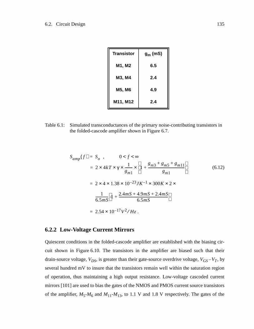
6.2. Circuit Design 135
(6.12)
6.2.2 Low-Voltage Current Mirr ors
Quiescent conditions in the folded-cascode amplifier are established with the biasing cir-
cuit shown in Figure6.10. The transistors in the amplifier are biased such that their
drain-source voltage,VDS, is greater than their gate-source overdrive voltage,VGS–VT, by
several hundred mV to insure that the transistors remain well within the saturation region
of operation, thus maintaining a high output resistance. Low-voltage cascoded current
mirrors [101] are used to bias the gates of the NMOS and PMOS current source transistors
of the amplifier, M5-M6 andM11-M13, to 1.1 V and 1.8 V respectively. The gates of the
Transistor gm (mS)
M1, M2 6.5
M3, M4 2.4
M5, M6 4.9
M11, M12 2.4
Table 6.1: Simulated transconductances of the primary noise-contributing transistors inthe folded-cascode amplifier shown in Figure6.7.
2 4 1.38 10 23–××× JK 1– 300K 2×× ×=
16.5mS--------------- 1 2.4mS 4.9mS 2.4mS+ +
6.5mS-----------------------------------------------------------+
2.54 10 17– V× 2 Hz⁄=
2 4kT γ 1gm1---------××× 1
gm3 gm5 gm11+ +
gm1--------------------------------------------+
×=
Samp f( ) So ,= 0 f ∞< <
.
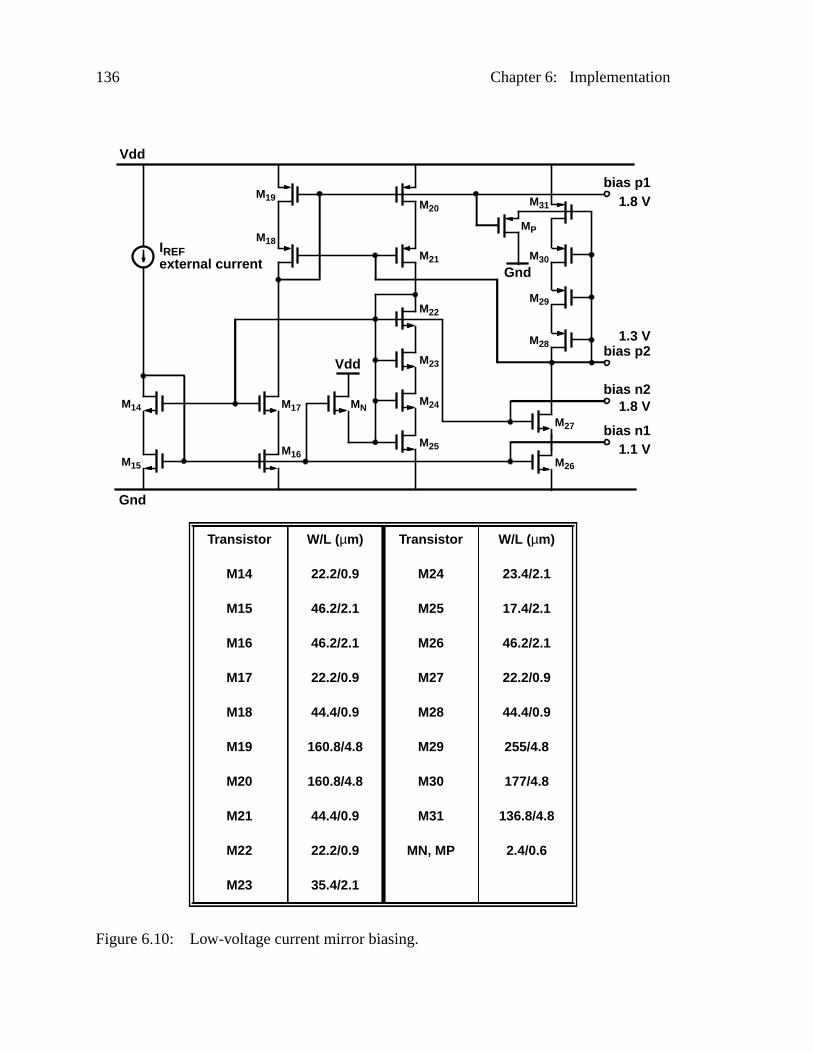
136 Chapter 6: Implementation
bias n1
bias p1
bias n2
bias p2
external current
Vdd
Gnd
Vdd
Gnd
M14
M15
M19
M18
MN
M16
M17
M22
M23
M24
M25
M21
M20
M28
M29
M30
M31
MP
M26
M27
Transistor W/L (µm) Transistor W/L (µm)
M14 22.2/0.9 M24 23.4/2.1
M15 46.2/2.1 M25 17.4/2.1
M16 46.2/2.1 M26 46.2/2.1
M17 22.2/0.9 M27 22.2/0.9
M18 44.4/0.9 M28 44.4/0.9
M19 160.8/4.8 M29 255/4.8
M20 160.8/4.8 M30 177/4.8
M21 44.4/0.9 M31 136.8/4.8
M22 22.2/0.9 MN, MP 2.4/0.6
M23 35.4/2.1
Figure6.10: Low-voltage current mirror biasing.
1.8 V
1.1 V
1.3 V
1.8 V
IREF
6.2. Circuit Design 137
NMOS cascode transistors,M7 andM8, are biased with a string of devices,M22-M25, that
are operated in the linear region [102]. The NMOS cascode bias voltage,bias_n2, is set at
a nominal value of 1.8 V. This is a compromise that ensures the NMOS current source
transistors,M3-M6, are saturated while allowing for a relatively large swing at the ampli-
fier’s outputs. Similarly, the gates of the PMOS cascode transistors,M9 and M10, are
biased by a string of devices in their linear region,M28-M31, to a nominal voltage of 1.3 V.
Small transistors,MN andMP, insure that the bias circuit settles to the desired operating
point instead of a stable, zero-current state. All transistors in Figure6.10, with the excep-
tion of MN andMP, have nonminimum channel lengths in order to reduce the influence of
channel length modulation on the bias voltages. The operating conditions in the bias cir-
cuit are established with an external reference current,IREF, that is applied toM14 and
M15 and mirrored in the different branches of the circuit. In order to reduce layout com-
plexity, but at the expense of increased power dissipation, the experimental modulator
contains four independent biasing circuits, one for each operational amplifier.
6.2.3 Comparator
The two 1-b quantizers in Figure5.9 are realized using a fast dynamic latch [103] fol-
lowed by buffers and a set-reset (SR) latch that holds the data for a full clock cycle. The
dynamic latch is shown in Figure6.11. Preamplification is not required because each path
of the proposed modulator is relatively insensitive to errors introduced at the inputs to the
respective quantizers. However, as discussed in Section5.3.1, gross mismatch of offset
and hysteresis between the two quantizers can generate tones in the output spectrum at dc
and fs/2, as well as adversely affect the degree of mirror signal suppression that is
achieved at the output of the modulator. In the interest of reducing the input-referred off-
sets of each quantizer, nonminimum channel length transistors are used in the regenerative
cores of both comparators.
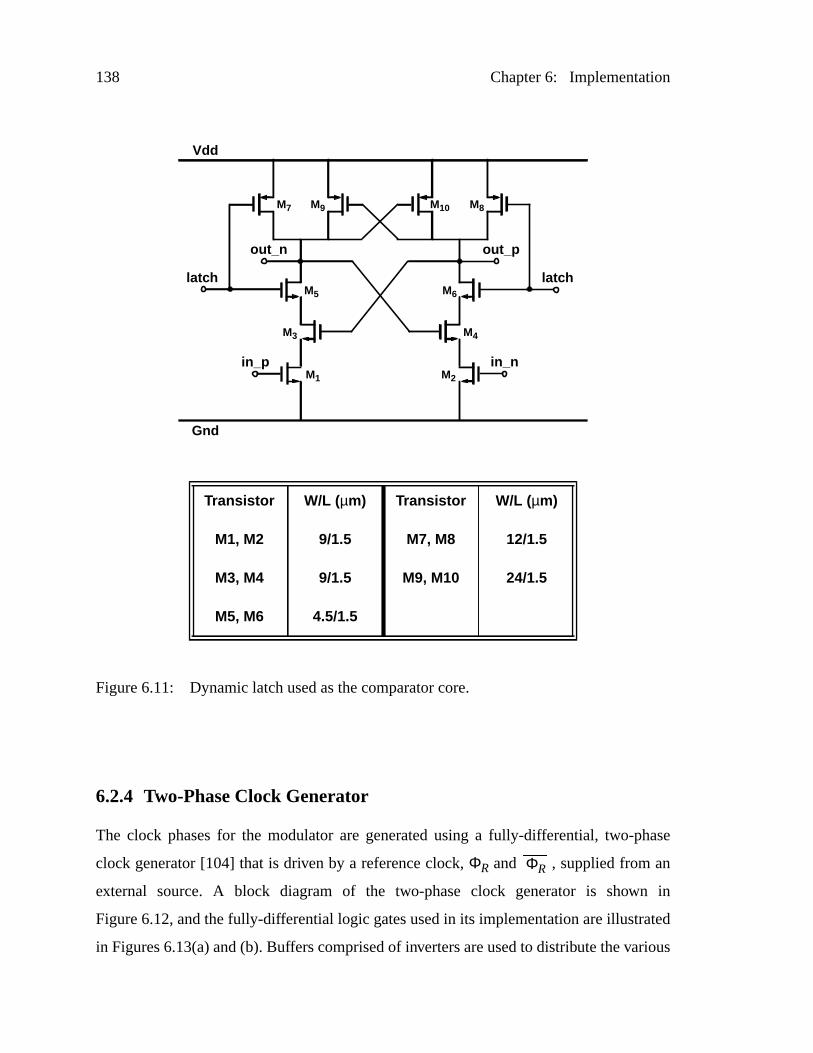
138 Chapter 6: Implementation
6.2.4 Two-Phase Clock Generator
The clock phases for the modulator are generated using a fully-differential, two-phase
clock generator [104] that is driven by a reference clock,ΦR and , supplied from an
external source. A block diagram of the two-phase clock generator is shown in
Figure6.12, and the fully-differential logic gates used in its implementation are illustrated
in Figures 6.13(a) and (b). Buffers comprised of inverters are used to distribute the various
M1
Vdd
Gnd
in_p in_n
out_n
latc h
out_p
latc h
M3
M7
M5
M9
M2
M4
M8
M6
M10
Transistor W/L (µm) Transistor W/L (µm)
M1, M2 9/1.5 M7, M8 12/1.5
M3, M4 9/1.5 M9, M10 24/1.5
M5, M6 4.5/1.5
Figure6.11: Dynamic latch used as the comparator core.
ΦR
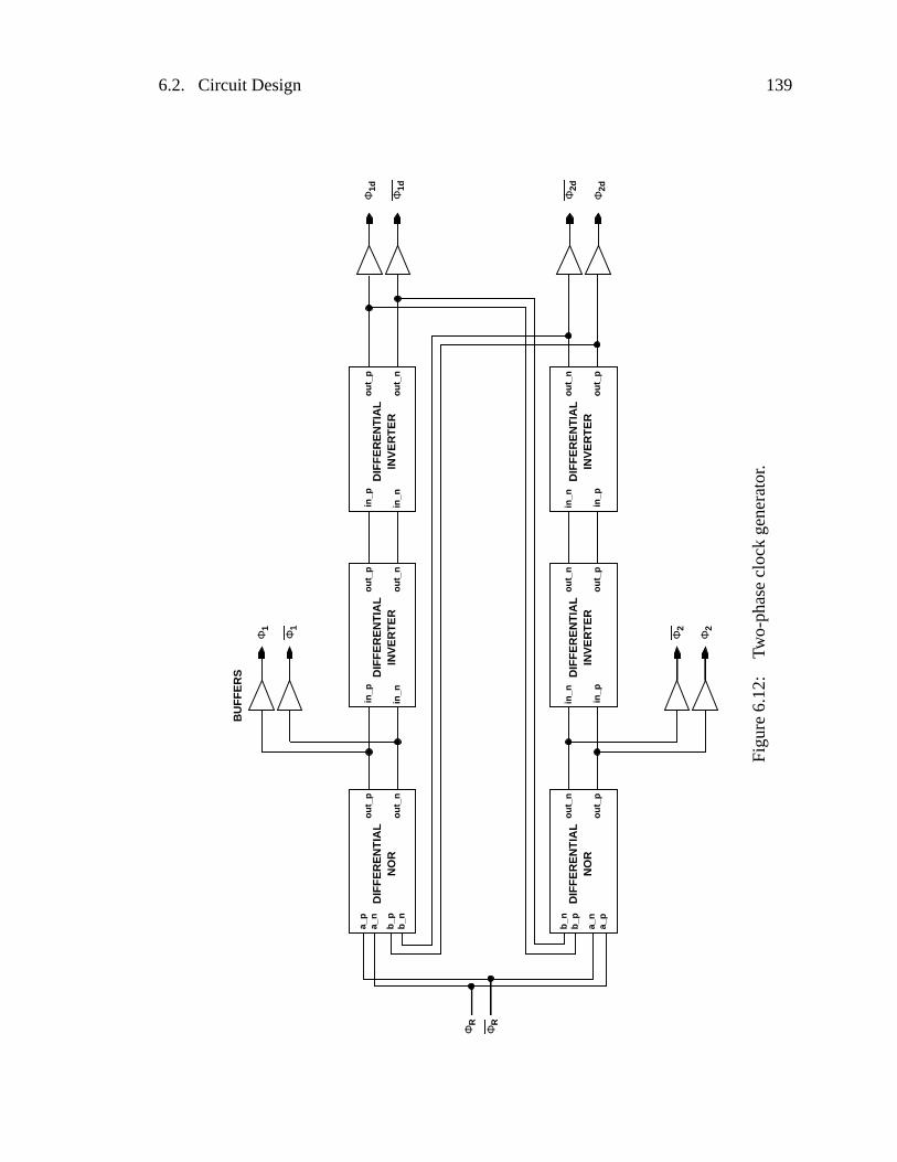
6.2. Circuit Design 139
DIF
FE
RE
NT
IAL
NO
R
a_n
a_p
b_p
b_n
out_
p
out_
n
DIF
FE
RE
NT
IAL
INV
ER
TE
R
in_p
in_n
out_
p
out_
n
DIF
FE
RE
NT
IAL
INV
ER
TE
R
in_p
in_n
out_
p
out_
n
NO
RD
IFF
ER
EN
TIA
L
a_n
a_p
b_p
b_n
out_
p
out_
n
INV
ER
TE
RD
IFF
ER
EN
TIA
L
in_p
in_n
out_
p
out_
n
INV
ER
TE
RD
IFF
ER
EN
TIA
L
in_p
in_n
out_
p
out_
n
BU
FF
ER
S
ΦR
Φ1
Φ1d
ΦR
Φ2d
Φ1d
Φ2
Φ1
Φ2
Φ2d
Fig
ure
6.12
:Tw
o-ph
ase
cloc
k ge
nera
tor
.
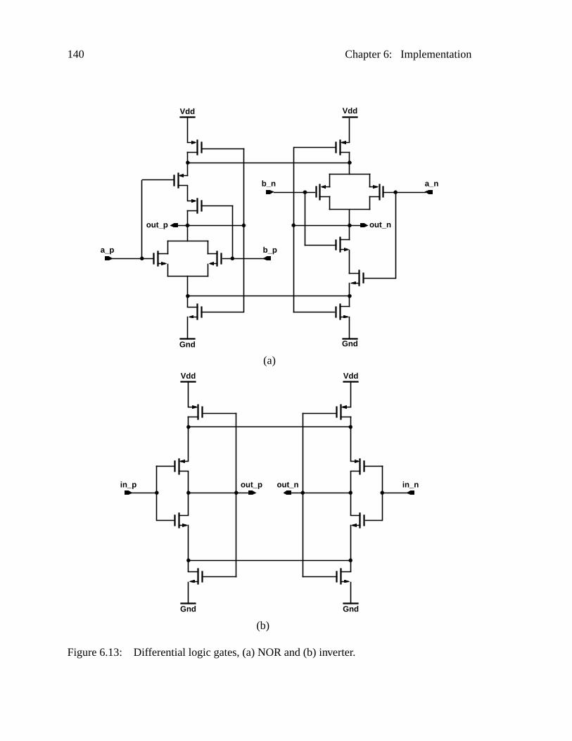
140 Chapter 6: Implementation
Figure6.13: Differential logic gates, (a) NOR and (b) inverter.
Vdd
Gnd Gnd
Vdd
b_n a_n
b_pa_p
out_nout_p
Vdd
Gnd
in_p
Vdd
Gnd
in_nout_p out_n
(a)
(b)
6.3. Noise Analysis of the Proposed Two-Path Modulator 141
clock phases throughout the chip. The use of a fully-differential clock topology is espe-
cially convenient in this application because the complements of the clocks are generated
automatically, without the use of any additional inverters. Therefore, the potential for
introducing skew between clocks and their complements is avoided.
6.2.5 Output Dri vers
The outputs from the comparators are brought off chip as fully-differential, current-mode
signals using the driver shown in Figure6.14. The open drains of the differential pair com-
prised ofM4 andM5 are connected to 100Ω pullup resistors on the test board, which are
tied to an external 3.3 V power supply that is not shared with the integrated circuit. The
tail current source,M3, is biased to approximately 1 mA by diode-connected transistors
M1 andM2.
The use of current-mode outputs with small pullup resistors ensures that the voltage
swings across the bond wires is small, thus reducing the amount of noise coupling through
mutual inductance to adjacent sensitive nodes. Also, since the voltage swing at the output
pads is small, the amount of noise injected into the substrate through the large parasitic
capacitance that exists between the pad and substrate is minimized.
6.3 Noise Analysis of the Proposed Two-PathModulator
Section6.1.3 and Section6.1.4 discussed the effects of switch and amplifier noise on the
performance of the switched-capacitor highpass path filter depicted in Figure6.1. The fol-
lowing section extends this discussion to the entire two-path modulator. The total inband
noise power of the two-path modulator is estimated assuming that quantization noise is
negligible with respect to switch and amplifier noise in the circuit.
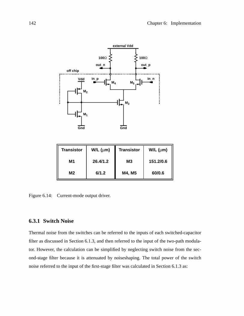
142 Chapter 6: Implementation
6.3.1 Switch Noise
Thermal noise from the switches can be referred to the inputs of each switched-capacitor
filter as discussed in Section6.1.3, and then referred to the input of the two-path modula-
tor. However, the calculation can be simplified by neglecting switch noise from the sec-
ond-stage filter because it is attenuated by noiseshaping. The total power of the switch
noise referred to the input of the first-stage filter was calculated in Section6.1.3 as:
Figure6.14: Current-mode output driver.
Vdd
Gnd
in_p
Gnd
in_n
external Vdd
off chip
100Ω 100Ω
M1
M2
M3
M4 M5
Transistor W/L (µm) Transistor W/L (µm)
M1 26.4/1.2 M3 151.2/0.6
M2 6/1.2 M4, M5 60/0.6
out_n out_p
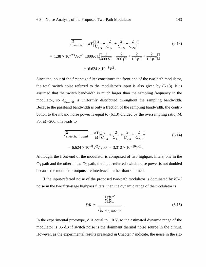
6.3. Noise Analysis of the Proposed Two-Path Modulator 143
(6.13)
Since the input of the first-stage filter constitutes the front-end of the two-path modulator,
the total switch noise referred to the modulator’s input is also given by (6.13). It is
assumed that the switch bandwidth is much larger than the sampling frequency in the
modulator, so is uniformly distributed throughout the sampling bandwidth.
Because the passband bandwidth is only a fraction of the sampling bandwidth, the contri-
bution to the inband noise power is equal to (6.13) divided by the oversampling ratio,M.
For M=200, this leads to
(6.14)
Although, the front-end of the modulator is comprised of two highpass filters, one in the
Φ1 path and the other in theΦ2 path, the input-referred switch noise power is not doubled
because the modulator outputs are interleaved rather than summed.
If the input-referred noise of the proposed two-path modulator is dominated bykT/C
noise in the two first-stage highpass filters, then the dynamic range of the modulator is
. (6.15)
In the experimental prototype,∆ is equal to 1.0 V, so the estimated dynamic range of the
modulator is 86 dB if switch noise is the dominant thermal noise source in the circuit.
However, as the experimental results presented in Chapter 7 indicate, the noise in the sig-
eswi tch2
kT2
C1A---------- 2
C1B---------- 2
C2A---------- 2
C2B----------+ + +
=
1.38 10 23– JK 1–× 300K2
300fF---------------- 2
300fF---------------- 2
1.5pF--------------- 2
1.5pF---------------+ + +
⋅⋅=
6.624 10 8–× V2= .
eswi tch2
eswi tch inband,2 kT
M------ 2
C1A---------- 2
C1B---------- 2
C2A---------- 2
C2B----------+ + +
=
6.624 10 8–× V2 200⁄= 3.312 10 10–× V2= .
DR
12--- ∆
2---
2
eswi tch inband,2
-----------------------------------=
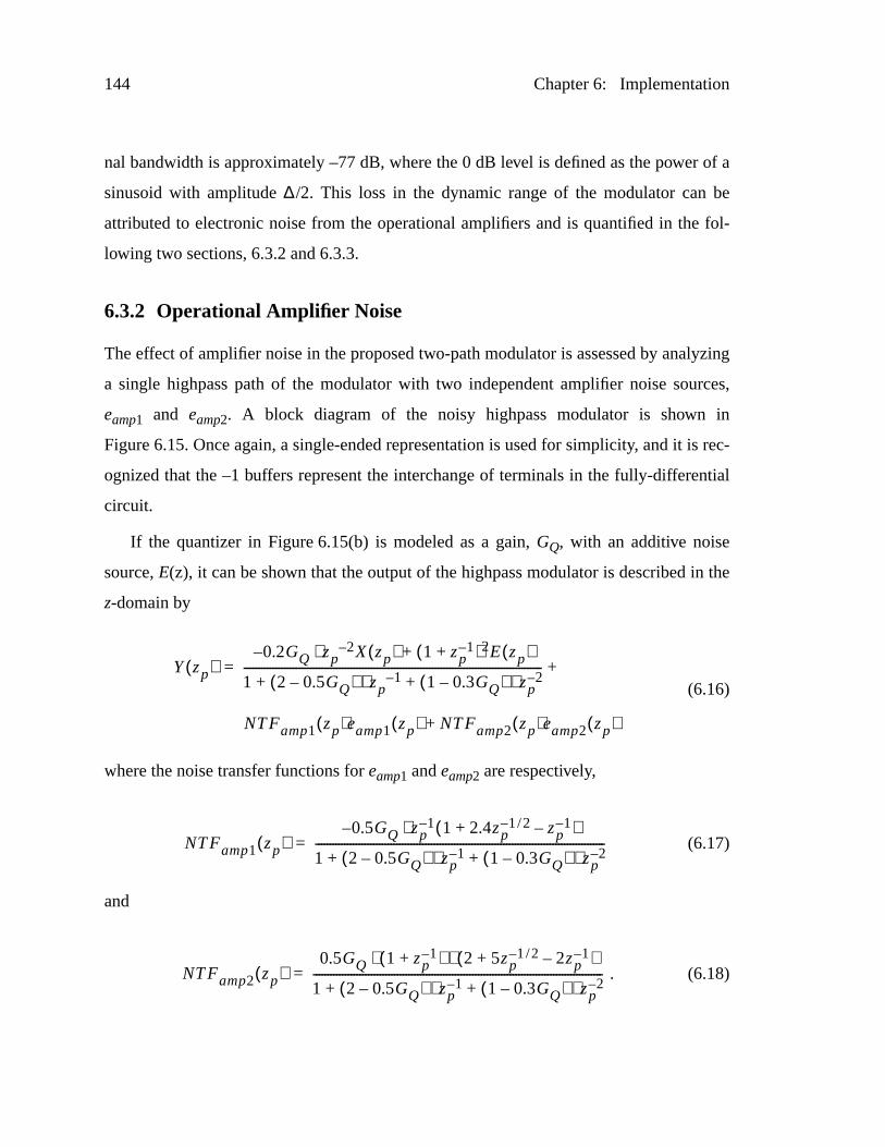
144 Chapter 6: Implementation
nal bandwidth is approximately –77 dB, where the 0 dB level is defined as the power of a
sinusoid with amplitude∆/2. This loss in the dynamic range of the modulator can be
attributed to electronic noise from the operational amplifiers and is quantified in the fol-
lowing two sections, 6.3.2 and 6.3.3.
6.3.2 Operational Amplifier Noise
The effect of amplifier noise in the proposed two-path modulator is assessed by analyzing
a single highpass path of the modulator with two independent amplifier noise sources,
eamp1 and eamp2. A block diagram of the noisy highpass modulator is shown in
Figure6.15. Once again, a single-ended representation is used for simplicity, and it is rec-
ognized that the –1 buffers represent the interchange of terminals in the fully-differential
circuit.
If the quantizer in Figure6.15(b) is modeled as a gain, GQ, with an additive noise
source,E(z), it can be shown that the output of the highpass modulator is described in the
z-domain by
(6.16)
where the noise transfer functions foreamp1 andeamp2 are respectively,
(6.17)
and
. (6.18)
Y zp( )0.2GQ zp⋅ 2– X zp( ) 1 zp
1–+( )2E zp( )+–
1 2 0.5GQ–( ) zp⋅ 1– 1 0.3GQ–( ) zp2–⋅++
------------------------------------------------------------------------------------------------------- +=
NTFamp1 zp( )eamp1 zp( ) NTFamp2 zp( )eamp2 zp( )+
NTFamp1 zp( )0.5– GQ zp
1– 1 2.4zp1 2/– zp
1––+( )⋅
1 2 0.5GQ–( ) zp1– 1 0.3GQ–( ) zp
2–⋅+⋅+----------------------------------------------------------------------------------------------------=
NTFamp2 zp( )0.5GQ 1 zp
1–+( ) 2 5zp1 2/– 2zp
1––+( )⋅ ⋅
1 2 0.5GQ–( ) zp1– 1 0.3GQ–( ) zp
2–⋅+⋅+----------------------------------------------------------------------------------------------------=
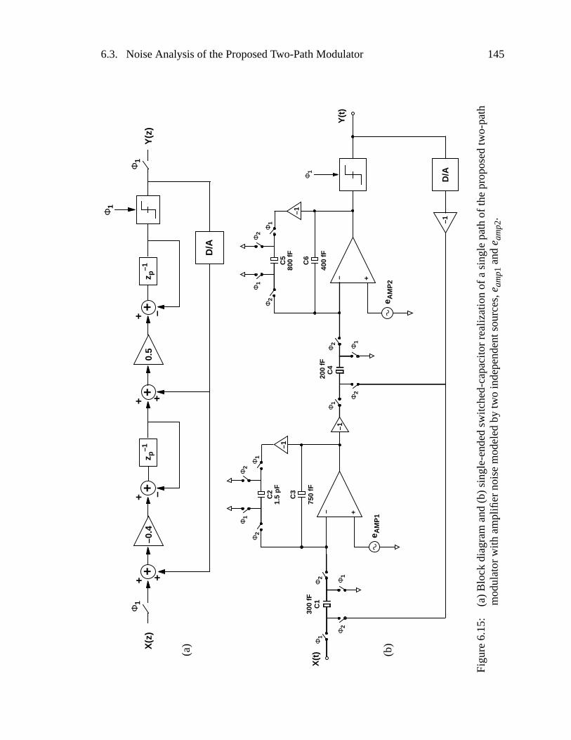
6.3. Noise Analysis of the Proposed Two-Path Modulator 145
Fig
ure
6.15
:(a
) B
lock
dia
gram
and
(b)
sin
gle-
ende
d sw
itche
d-ca
paci
tor
real
izat
ion
of a
sin
gle
path
of t
he p
ropo
sed
two-
path
mod
ulat
or w
ith a
mpl
ifier
noi
se m
odel
ed b
y two in
depe
nden
t sou
rces
,e a
mp1
and
e am
p2.Φ
1
X(z
)Φ
1Φ
1
Y(z
)0.
5z p
–1–0
.4z p
–1
D/A
+ –++ ++
+ +++ –+
+–
Φ2
Φ2
Φ1
Φ1
C2
C3
Φ2
Φ2
Φ1
Φ1
C1
–1
X(t
)
e AM
P1
+–
Φ2
Φ2
Φ1
Φ1
C5
C6
Y(t
)Φ
2
Φ2
Φ1
Φ1
C4
–1
e AM
P2
–1
Φ1
D/A
–1
300
fF
200
fF40
0 fF
800
fF
750
fF
1.5
pF
(a)
(b)
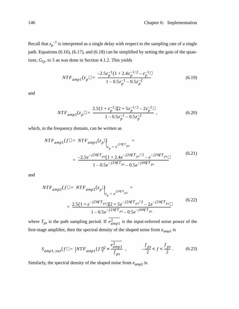
146 Chapter 6: Implementation
Recall thatzp–1 is interpreted as a single delay with respect to the sampling rate of a single
path. Equations (6.16), (6.17), and (6.18) can be simplified by setting the gain of the quan-
tizer, GQ, to 5 as was done in Section4.1.2. This yields
(6.19)
and
, (6.20)
which, in the frequency domain, can be written as
(6.21)
and
(6.22)
whereTps is the path sampling period. If is the input-referred noise power of the
first-stage amplifier, then the spectral density of the shaped noise fromeamp1 is
. (6.23)
Similarly, the spectral density of the shaped noise fromeamp2 is
NTFamp1 zp( )2.5– zp
1– 1 2.4zp1 2/– zp
1––+( )
1 0.5zp1– 0.5zp
2–––--------------------------------------------------------------------=
NTFamp2 zp( )2.5 1 zp
1–+( ) 2 5zp1 2/– 2zp
1––+( )
1 0.5zp1–– 0.5zp
2––------------------------------------------------------------------------------=
NTFamp1 f( ) NTFamp1 zp( )zp e
j2πf Tps=
= =
2.5ej2πf Tps–
1 2.4ej2πf Tps 2⁄–
ej2πf Tps–
–+( )–
1 0.5ej2πf Tps–
– 0.5ej4πf Tps–
–--------------------------------------------------------------------------------------------------------------------=
NTFamp2 f( ) NTFamp2 zp( )zp e
j2πf Tps=
= =
2.5 1 e+j2πf Tps–( ) 2 5e
j2πf Tps 2⁄–2e
j2πf Tps––+( )
1 0.5ej2πf Tps–
– 0.5ej4πf Tps–
–------------------------------------------------------------------------------------------------------------------------------=
eamp12
Samp1 out, f( ) NTFamp1 f( ) 2eamp1
2
f ps---------------× ,=
f ps
2-------- f
f ps
2--------< <–
6.3. Noise Analysis of the Proposed Two-Path Modulator 147
(6.24)
given that is the input-referred noise power of the second-stage amplifier.
Next, it is noted that the signal passband is centered at± fps/2, and the passband band-
width is assumed to be much less thanfps. Therefore, in the passband, the spectral density
of the shaped noise fromeamp1 andeamp2 can be approximated as
(6.25)
and
(6.26)
The important and disturbing implication of (6.25) is that within the passband, noise
power from the first-stage amplifier is amplified by a factor of 61 at the output of the filter.
Fortunately, (6.26) indicates that the inband noise contribution from the second-stage
amplifier is negligible because the noise shaping functionNTFamp2( f ) has a zero atfps/2.
From (6.25) and (6.26), the power of the amplifier noise present in the signal band is
approximately
Samp2 out, f( ) NTFamp2 f( ) 2eamp2
2
f ps---------------× ,=
f ps
2-------- f
f ps
2--------< <–
eamp22
Samp1 inband, f( ) Samp1 out, f( )f f ps 2⁄=
≈
61eamp1
2
f ps---------------×=
NTFamp1 f( )f f ps 2⁄=
2eamp1
2
f ps---------------×=
Samp2 inband, f( ) Samp2 out, f( )f f ps 2⁄=
≈
0eamp2
2
f ps---------------×= 0=
NTFamp2 f( )f f ps 2⁄=
2eamp2
2
f ps---------------×=
.
148 Chapter 6: Implementation
(6.27)
whereB is the width of the passband.
The value of for the prototype modulator can be estimated from (6.27)
once has been calculated. From (6.7),
(6.28)
whereSo is the input-referred amplifier white noise density, andτcl is the closed-loop set-
tling time constant of the highpass path filter. In Section6.2.1, it is estimated that
So = 2.54×10⁻¹⁷V 2/Hz andτcl = 1.5 ns for the folded-cascode amplifier used in the proto-
type modulator. Therefore, by (6.28), this amplifier’s input-referred noise power, , is
approximately4.23×10–9 V2. Given a path sampling frequency, fps, of 40MHz, and pass-
band bandwidth,B, of 200kHz, the estimated contribution to the total output noise power
from eamp1 andeamp2 is
(6.29)
Once again, although the experimental prototype is comprised of two interleaved highpass
modulators, the output-referred amplifier noise of the entire two-path modulator is not
twice the value calculated in (6.29) because the outputs are interleaved, not summed. In
comparison with (6.14), it can be seen that inband noise contributed by the first-stage
amplifier is several times larger than the inbandkT/C noise.
eamp inband,2 Samp1 inband, f( ) Samp2 inband, f( )+[ ] B×≈
61eamp1
2
f ps---------------× B×≈
eamp inband,2
eamp12
eamp2 So
12πτcl------------- π
2---××=
eamp12
eamp inband,2 61
eamp12
f ps---------------× B×≈
614.23 10 9– V2×
40MHz-----------------------------------× 200kHz×=
1.29 10 9–× V2= .
6.4. Summary 149
6.3.3 Calculated Front-End Noise
If it is assumed that quantization noise is negligible with respect to switch and amplifier
noise, the estimated dynamic range of the two-path modulator with∆ = 1.0 V is
(6.30)
This estimate is confirmed by the experimental results presented in Chapter 7; the mea-
sured inband noise power of the prototype modulator is approximately 77 dB below over-
load (0 dB), which is defined as the power of a sinusoid with amplitude∆/2.
6.4 Summary
The implementation of the proposed two-path,fs/4 modulator has been described in this
chapter. A fully-dif ferential, switched-capacitor path filter that implements the desired
highpass transfer function has been designed, and its limitations due to switch and ampli-
fier noise, as well as finite amplifier gain and bandwidth, have been analyzed. Although
the use of the two-path modulator topology relaxes the settling requirements on the opera-
tional amplifiers, behavioral simulations indicate that the amplifiers must still have at least
5 to 6 time constants to settle because small mismatches in the settling times between the
two paths will degrade the suppression of the mirror signal. A folded-cascode amplifier
with a closed-loop, simulated settling time constant of approximately 2 ns was designed to
meet these requirements when the path filter is clocked at 40 MHz. The amplifier is biased
by low-voltage current mirrors that are programmed by an external current.
DR
12--- ∆
2---
2
eswi tch inband,2 eamp inband,
2+------------------------------------------------------------------------=
12--- 1.0V
2-----------
2
3.312 10 10– V2 1.29 10 9– V2×+×-----------------------------------------------------------------------------------=
7.71 107×= 79 dB= .
150 Chapter 6: Implementation
Additional circuits in the prototype described in this chapter include the dynamic com-
parators, a two-phase clock generator, and the output drivers. The comparators are simple
regenerative cores followed by buffers and SR latches. The two-phase clock generator is
implemented using fully-differential logic gates so that the necessary clock phases and
their complements can be generated without introducing unnecessary skew between the
clocks and their complements. The output drivers bring the one-bit data streams from each
path off chip as fully-differential current-mode signals to reduce the amount of noise cou-
pling through bond wire mutual inductance, substrate injection, and power supply distur-
bance.
A noise analysis of the entire two-path modulator reveals that the noise floor of the
experimental prototype is dominated by a combination of amplifier noise and thermal
noise from the switches. As a strong caveat, it is noted that amplifier noise in the
first-stage path filter is shaped to have a maximum spectral density in the signal band cen-
tered atfs/4. This hazardous noise amplification can degrade the dynamic range of the
modulator by a substantial margin if some care is not taken to design an operational ampli-
fier with a low enough input-referred noise power such that at the output of the modulator,
the level of shaped amplifier noise in the passband remains comparable to the level of
inbandkT/C noise.
151
Chapter
7 Experimental Results
An experimental prototype of the proposed two-path,fs/4 modulator described in the pre-
ceding chapters has been fabricated in a 0.6-µm, single-poly, triple-metal CMOS process
through the MOSIS service. When operated from a 3.3-V supply, the experimental modu-
lator dissipates 49 mW, and the clock generator dissipates an additional 23 mW. An esti-
mated 40% of the power dissipated in the analog circuitry is devoted to driving the large
bottom-plate parasitics of the feedback and sampling capacitances. Thus, the power dissi-
pation could be reduced significantly in a technology with a smaller bottom-plate para-
sitic. Also, the currents and device sizes in the second stage of the modulator could be
scaled more aggressively. In this prototype, to expedite the design, the first and second
stages of the modulator were implemented using identical operational amplifiers. Only
capacitances were scaled in the second stage.
This chapter describes the layout of the prototype chip, the test setup used to charac-
terize the experimental circuit, and the measured results.
7.1 Layout
A die photo of the experimental prototype is shown in Figure7.1. Mirror symmetry was
observed in the layout to enhance the rejection of common-mode disturbances in the
fully-dif ferential circuit. The front-end, differential inputs to the modulator are at the far
left of the die. The digital circuits, seen at the right of Figure7.1, are physically separated
from the analog circuits and are powered from a separate supply. The use of different ana-
log and digital supplies decouples the analog circuitry from the switching noise caused by
large dynamic currents drawn from the digital supply.
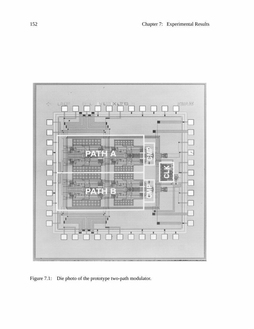
152 Chapter 7: Experimental Results
Figure7.1: Die photo of the prototype two-path modulator.
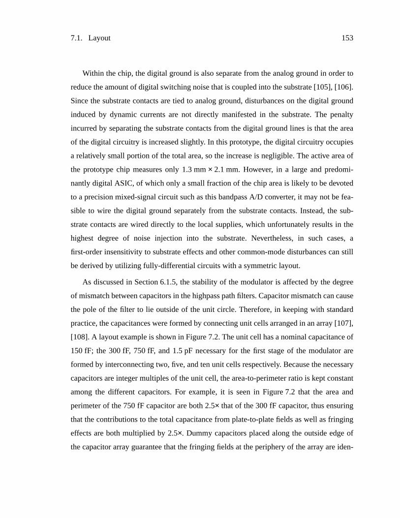
7.1. Layout 153
Within the chip, the digital ground is also separate from the analog ground in order to
reduce the amount of digital switching noise that is coupled into the substrate [105], [106].
Since the substrate contacts are tied to analog ground, disturbances on the digital ground
induced by dynamic currents are not directly manifested in the substrate. The penalty
incurred by separating the substrate contacts from the digital ground lines is that the area
of the digital circuitry is increased slightly. In this prototype, the digital circuitry occupies
a relatively small portion of the total area, so the increase is negligible. The active area of
the prototype chip measures only 1.3mm × 2.1mm. However, in a large and predomi-
nantly digital ASIC, of which only a small fraction of the chip area is likely to be devoted
to a precision mixed-signal circuit such as this bandpass A/D converter, it may not be fea-
sible to wire the digital ground separately from the substrate contacts. Instead, the sub-
strate contacts are wired directly to the local supplies, which unfortunately results in the
highest degree of noise injection into the substrate. Nevertheless, in such cases, a
first-order insensitivity to substrate effects and other common-mode disturbances can still
be derived by utilizing fully-differential circuits with a symmetric layout.
As discussed in Section6.1.5, the stability of the modulator is affected by the degree
of mismatch between capacitors in the highpass path filters. Capacitor mismatch can cause
the pole of the filter to lie outside of the unit circle. Therefore, in keeping with standard
practice, the capacitances were formed by connecting unit cells arranged in an array [107],
[108]. A layout example is shown in Figure7.2. The unit cell has a nominal capacitance of
150fF; the 300fF, 750fF, and 1.5pF necessary for the first stage of the modulator are
formed by interconnecting two, five, and ten unit cells respectively. Because the necessary
capacitors are integer multiples of the unit cell, the area-to-perimeter ratio is kept constant
among the different capacitors. For example, it is seen in Figure7.2 that the area and
perimeter of the 750 fF capacitor are both 2.5× that of the 300 fF capacitor, thus ensuring
that the contributions to the total capacitance from plate-to-plate fields as well as fringing
effects are both multiplied by 2.5×. Dummy capacitors placed along the outside edge of
the capacitor array guarantee that the fringing fields at the periphery of the array are iden-
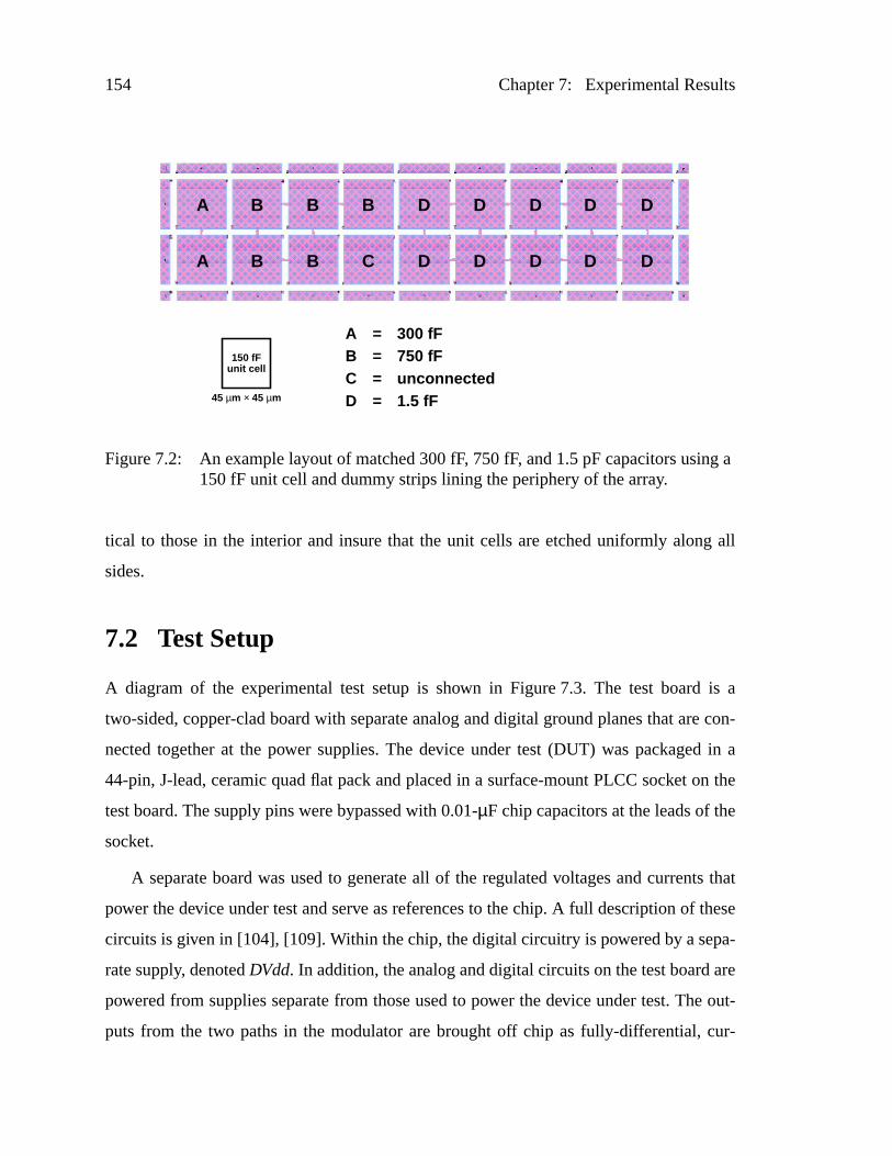
154 Chapter 7: Experimental Results
tical to those in the interior and insure that the unit cells are etched uniformly along all
sides.
7.2 Test Setup
A diagram of the experimental test setup is shown in Figure7.3. The test board is a
two-sided, copper-clad board with separate analog and digital ground planes that are con-
nected together at the power supplies. The device under test (DUT) was packaged in a
44-pin, J-lead, ceramic quad flat pack and placed in a surface-mount PLCC socket on the
test board. The supply pins were bypassed with 0.01-µF chip capacitors at the leads of the
socket.
A separate board was used to generate all of the regulated voltages and currents that
power the device under test and serve as references to the chip. A full description of these
circuits is given in [104], [109]. Within the chip, the digital circuitry is powered by a sepa-
rate supply, denotedDVdd. In addition, the analog and digital circuits on the test board are
powered from supplies separate from those used to power the device under test. The out-
puts from the two paths in the modulator are brought off chip as fully-differential, cur-
ABCD
A
A
B
B
B
CB
B D D D D D
D D D D D
Figure7.2: An example layout of matched 300 fF, 750 fF, and 1.5 pF capacitors using a150fF unit cell and dummy strips lining the periphery of the array.
= 300 fF= 750 fF
= 1.5 fFunconnected=
45 µm × 45 µm
150 fFunit cell
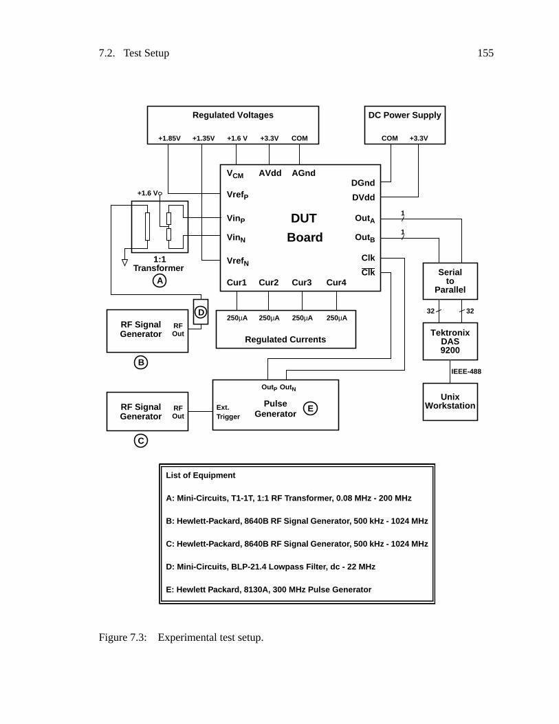
7.2. Test Setup 155
Boar d
DUT
GeneratorPulse
VinN
VinP
OutP OutN
Trig gerExt.
OutA
OutB
GeneratorRF Signal
OutRF
Regulated Voltages
+1.6 V COM+3.3V
Clk
Clk
VrefP
VrefN
Cur1 Cur2 Cur3 Cur4
VCM AGnd
DVdd
AVddDGnd
+1.35V+1.85V
DC Power Supply
COM +3.3V
Regulated Currents
250µA 250µA250µA250µA
GeneratorRF Signal
OutRF
+1.6 V
1:1Transf ormer Serial
toParallel
TektronixDAS
UnixWorkstation
1
1
32 32
IEEE-488
Figure7.3: Experimental test setup.
9200
A
B
C
E
List of Equipment
A: Mini-Cir cuits, T1-1T , 1:1 RF Transf ormer , 0.08 MHz - 200 MHz
B: Hewlett-P ackard, 8640B RF Signal Generator , 500 kHz - 1024 MHz
C: Hewlett-P ackard, 8640B RF Signal Generator , 500 kHz - 1024 MHz
D: Mini-Cir cuits, BLP-21.4 Lo wpass Filter , dc - 22 MHz
E: Hewlett P ackard, 8130A, 300 MHz Pulse Generator
D
156 Chapter 7: Experimental Results
rent-mode signals, which are tied to pullup resistors on the test board as described in
Section6.2.5. The resulting low-swing voltage signals are amplified to full CMOS logic
levels by fast AD9696 comparators before being harvested by a custom serial-to-parallel
interface board.
The differential input to the modulator was generated by driving an external, cen-
ter-tapped transformer with the filtered output of a low phase noise, single-ended sinusoi-
dal source locked to various test frequencies near 20 MHz. The filter at the output of the
RF generator suppresses the higher-order harmonics of the input signal before they are
passed to the device under test. The differential sinusoid is applied directly to the inputs of
the modulator. The reference voltages of the modulator were tied toVREF+ = 1.85 V and
VREF– = 1.35 V. In the subsequent plots of performance as a function of the signal level,
0 dB corresponds to the power of a differential sine wave input of 1.0 Vp-p.
A low-swing, differential clock from an external pulse generator triggered by a low
phase-noise signal source locked at 40 MHz was brought on chip, amplified to full swing,
and then used to generate the requisite clock phases. The custom interface board collects
640,000 samples from each of the two independent paths of the modulator, A andB, and
then transfers this data to a workstation for interleaving, filtering, and analysis. Figure7.4
shows an FFT of the interleaved bitstream, prior to decimation, when a –10dB input sig-
nal is applied to the modulator.
The degree of mirror signal suppression in the modulator was evaluated by demodulat-
ing the bandpass signal to baseband with quadrature carriers in the digital domain and per-
forming an FFT on the resulting complex-valued signal,xI [n] – j xQ[n]. The spectrum of
the demodulated, complex-valued baseband signal is shown in Figure7.5. It is seen that
the mirror signal is suppressed by 42 dB with respect to the desired signal.
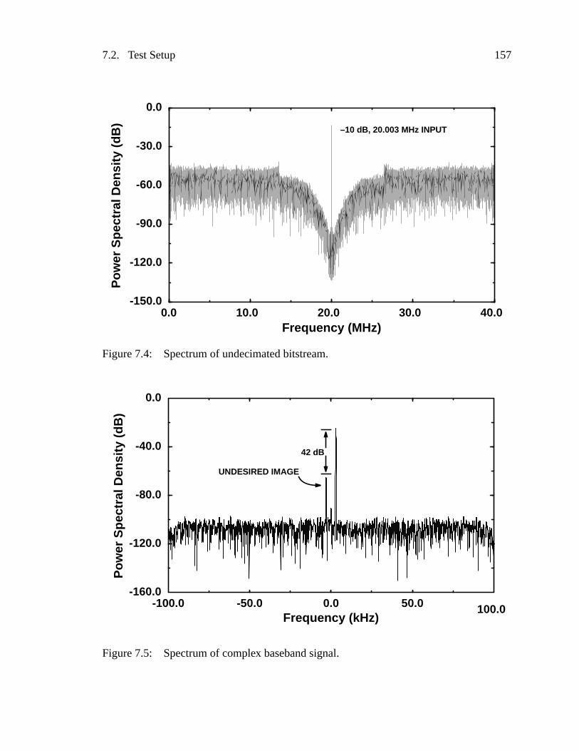
7.2. Test Setup 157
Figure7.4: Spectrum of undecimated bitstream.
0.0 10.0 20.0 30.0 40.0-150.0
-120.0
-90.0
-60.0
-30.0
0.0
–10 dB, 20.003 MHz INPUTP
ower
Spe
ctra
l Den
sity
(dB
)
Frequency (MHz)
-100.0 -50.0 0.0 50.0 100.0
-160.0
-120.0
-80.0
-40.0
0.0
Frequency (kHz)
Pow
er S
pect
ral D
ensi
ty (
dB)
UNDESIRED IMAGE
42 dB
Figure7.5: Spectrum of complex baseband signal.
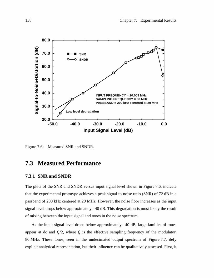
158 Chapter 7: Experimental Results
7.3 Measured Performance
7.3.1 SNR and SNDR
The plots of the SNR and SNDR versus input signal level shown in Figure7.6. indicate
that the experimental prototype achieves a peak signal-to-noise ratio (SNR) of 72dB in a
passband of 200 kHz centered at 20 MHz. However, the noise floor increases as the input
signal level drops below approximately –40 dB. This degradation is most likely the result
of mixing between the input signal and tones in the noise spectrum.
As the input signal level drops below approximately –40 dB, large families of tones
appear at dc andfs/2, wherefs is the effective sampling frequency of the modulator,
80MHz. These tones, seen in the undecimated output spectrum of Figure7.7, defy
explicit analytical representation, but their influence can be qualitatively assessed. First, it
-50.0 -40.0 -30.0 -20.0 -10.0 0.020.0
30.0
40.0
50.0
60.0
70.0
80.0
SNR
SNDR
Input Signal Level (dB)
Sig
nal-t
o-N
oise
+Dis
tort
ion
(dB
)
INPUT FREQUENCY = 20.003 MHzSAMPLING FREQUENCY = 80 MHzPASSBAND = 200 kHz centered at 20 MHz
Low level degradation
Figure7.6: Measured SNR and SNDR.
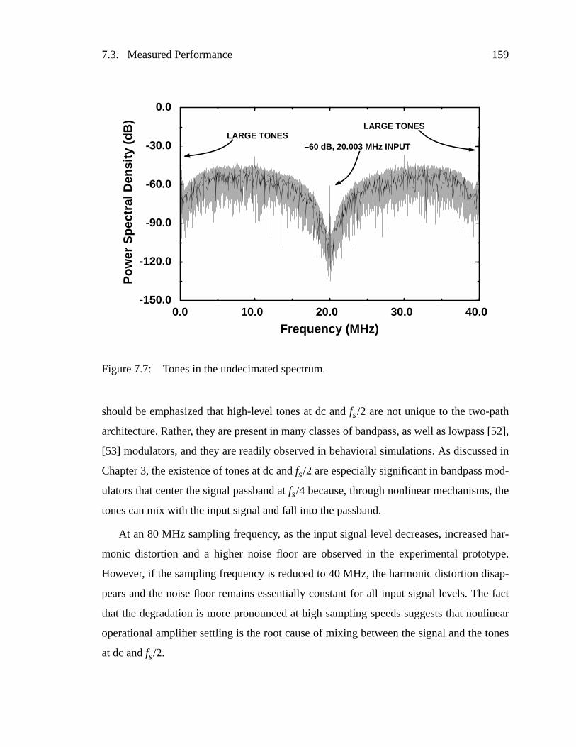
7.3. Measured Performance 159
should be emphasized that high-level tones at dc andfs/2 are not unique to the two-path
architecture. Rather, they are present in many classes of bandpass, as well as lowpass [52],
[53] modulators, and they are readily observed in behavioral simulations. As discussed in
Chapter 3, the existence of tones at dc andfs/2 are especially significant in bandpass mod-
ulators that center the signal passband atfs/4 because, through nonlinear mechanisms, the
tones can mix with the input signal and fall into the passband.
At an 80 MHz sampling frequency, as the input signal level decreases, increased har-
monic distortion and a higher noise floor are observed in the experimental prototype.
However, if the sampling frequency is reduced to 40 MHz, the harmonic distortion disap-
pears and the noise floor remains essentially constant for all input signal levels. The fact
that the degradation is more pronounced at high sampling speeds suggests that nonlinear
operational amplifier settling is the root cause of mixing between the signal and the tones
at dc andfs/2.
Figure7.7: Tones in the undecimated spectrum.
0.0 10.0 20.0 30.0 40.0-150.0
-120.0
-90.0
-60.0
-30.0
0.0
–60 dB, 20.003 MHz INPUTLARGE TONES
LARGE TONESP
ower
Spe
ctra
l Den
sity
(dB
)
Frequency (MHz)
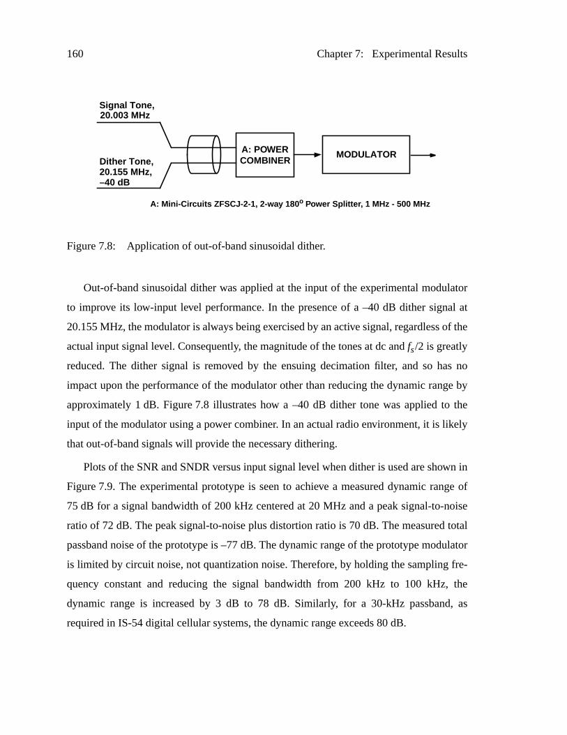
160 Chapter 7: Experimental Results
Out-of-band sinusoidal dither was applied at the input of the experimental modulator
to improve its low-input level performance. In the presence of a –40 dB dither signal at
20.155 MHz, the modulator is always being exercised by an active signal, regardless of the
actual input signal level. Consequently, the magnitude of the tones at dc andfs/2 is greatly
reduced. The dither signal is removed by the ensuing decimation filter, and so has no
impact upon the performance of the modulator other than reducing the dynamic range by
approximately 1dB. Figure7.8 illustrates how a –40 dB dither tone was applied to the
input of the modulator using a power combiner. In an actual radio environment, it is likely
that out-of-band signals will provide the necessary dithering.
Plots of the SNR and SNDR versus input signal level when dither is used are shown in
Figure7.9. The experimental prototype is seen to achieve a measured dynamic range of
75dB for a signal bandwidth of 200 kHz centered at 20 MHz and a peak signal-to-noise
ratio of 72 dB. The peak signal-to-noise plus distortion ratio is 70 dB. The measured total
passband noise of the prototype is –77 dB. The dynamic range of the prototype modulator
is limited by circuit noise, not quantization noise. Therefore, by holding the sampling fre-
quency constant and reducing the signal bandwidth from 200 kHz to 100 kHz, the
dynamic range is increased by 3 dB to 78 dB. Similarly, for a 30-kHz passband, as
required in IS-54 digital cellular systems, the dynamic range exceeds 80 dB.
MODULATOR
Signal Tone,
Dither Tone,A: POWERCOMBINER
20.003 MHz
20.155 MHz,–40 dB
Figure7.8: Application of out-of-band sinusoidal dither.
A: Mini-Cir cuits ZFSCJ-2-1, 2-wa y 180o Power Splitter , 1 MHz - 500 MHz
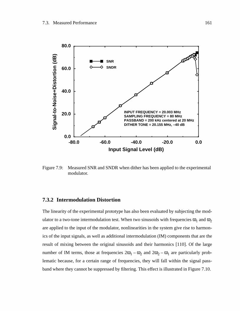
7.3. Measured Performance 161
7.3.2 Intermodulation Distortion
The linearity of the experimental prototype has also been evaluated by subjecting the mod-
ulator to a two-tone intermodulation test. When two sinusoids with frequenciesω1 andω2
are applied to the input of the modulator, nonlinearities in the system give rise to harmon-
ics of the input signals, as well as additional intermodulation (IM) components that are the
result of mixing between the original sinusoids and their harmonics [110]. Of the large
number of IM terms, those at frequencies 2ω1 – ω2 and 2ω2 – ω1 are particularly prob-
lematic because, for a certain range of frequencies, they will f all within the signal pass-
band where they cannot be suppressed by filtering. This effect is illustrated in Figure7.10.
Sig
nal-t
o-N
oise
+Dis
tort
ion
(dB
)
Input Signal Level (dB)-80.0 -60.0 -40.0 -20.0 0.0
0.0
20.0
40.0
60.0
80.0
SNR
SNDR
INPUT FREQUENCY = 20.003 MHzSAMPLING FREQUENCY = 80 MHzPASSBAND = 200 kHz centered at 20 MHzDITHER TONE = 20.155 MHz, –40 dB
Figure7.9: Measured SNR and SNDR when dither has been applied to the experimentalmodulator.
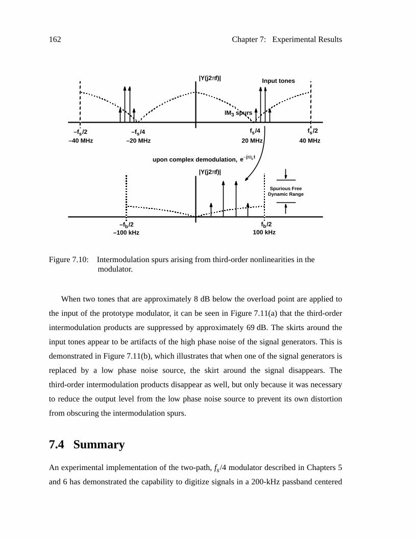
162 Chapter 7: Experimental Results
When two tones that are approximately 8 dB below the overload point are applied to
the input of the prototype modulator, it can be seen in Figure7.11(a) that the third-order
intermodulation products are suppressed by approximately 69dB. The skirts around the
input tones appear to be artifacts of the high phase noise of the signal generators. This is
demonstrated in Figure7.11(b), which illustrates that when one of the signal generators is
replaced by a low phase noise source, the skirt around the signal disappears. The
third-order intermodulation products disappear as well, but only because it was necessary
to reduce the output level from the low phase noise source to prevent its own distortion
from obscuring the intermodulation spurs.
7.4 Summary
An experimental implementation of the two-path,fs/4 modulator described in Chapters 5
and 6 has demonstrated the capability to digitize signals in a 200-kHz passband centered
fs /2fs /4–fs /4–fs /220 MHz 40 MHz–40 MHz –20 MHz
|Y(j2πf)|
fb /2100 kHz
–fb /2–100 kHz
|Y(j2πf)|
Input tones
upon comple x demodulation, e jωc t–
IM3 spur s
Figure7.10: Intermodulation spurs arising from third-order nonlinearities in themodulator.
Spurious FreeDynamic Rang e
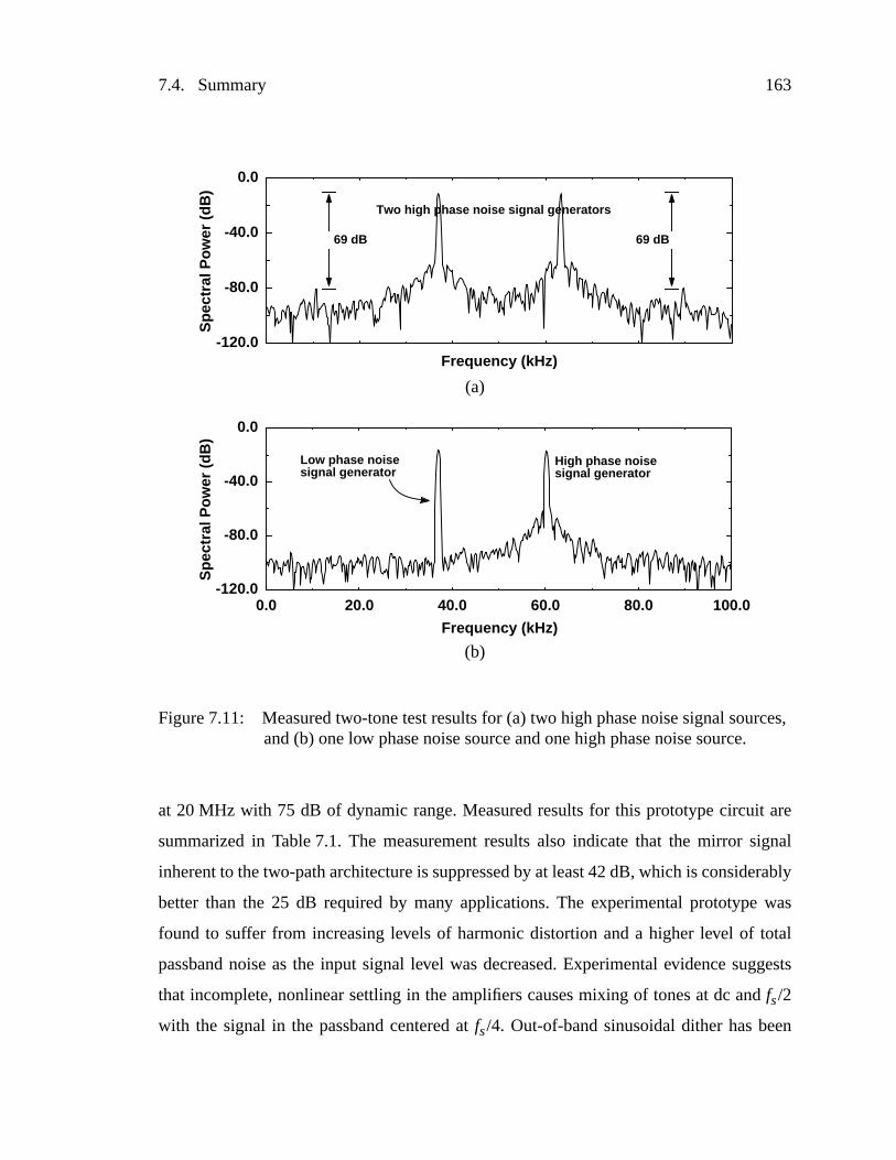
7.4. Summary 163
at 20MHz with 75 dB of dynamic range. Measured results for this prototype circuit are
summarized in Table7.1. The measurement results also indicate that the mirror signal
inherent to the two-path architecture is suppressed by at least 42 dB, which is considerably
better than the 25 dB required by many applications. The experimental prototype was
found to suffer from increasing levels of harmonic distortion and a higher level of total
passband noise as the input signal level was decreased. Experimental evidence suggests
that incomplete, nonlinear settling in the amplifiers causes mixing of tones at dc andfs/2
with the signal in the passband centered atfs/4. Out-of-band sinusoidal dither has been
-120.0
-80.0
-40.0
0.0
0.0 20.0 40.0 60.0 80.0 100.0-120.0
-80.0
-40.0
0.0
Frequency (kHz)
Spe
ctra
l Pow
er (
dB)
Spe
ctra
l Pow
er (
dB)
69 dB 69 dB
Two high phase noise signal generators
Low phase noisesignal generator
High phase noisesignal generator
(a)
(b)
Frequency (kHz)
Figure7.11: Measured two-tone test results for (a) two high phase noise signal sources,and (b) one low phase noise source and one high phase noise source.
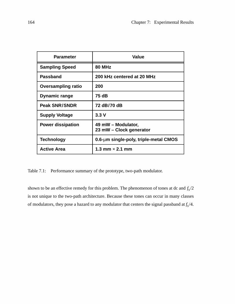
164 Chapter 7: Experimental Results
shown to be an effective remedy for this problem. The phenomenon of tones at dc andfs/2
is not unique to the two-path architecture. Because these tones can occur in many classes
of modulators, they pose a hazard to any modulator that centers the signal passband atfs/4.
Parameter Value
Sampling Speed 80 MHz
Passband 200 kHz centered at 20 MHz
Oversampling ratio 200
Dynamic rang e 75 dB
Peak SNR/SNDR 72 dB /70 dB
Suppl y Volta ge 3.3 V
Power dissipation 49 mW – Modulator ,23 mW – Cloc k generator
Technology 0.6-µm single-pol y, triple-metal CMOS
Active Area 1.3 mm × 2.1 mm
Table 7.1: Performance summary of the prototype, two-path modulator.
165
Chapter
8 Conclusion
8.1 Summary
To meet the anticipated requirements imposed by the myriad of next-generation networks
for wireless communications, substantial effort is currently being devoted to the develop-
ment of integrated receivers that are compatible with multiple standards. The investigation
of this design space involves tradeoffs between factors such as receiver dynamic range,
power dissipation and system linearity. In addition, digitization in the signal path is rap-
idly becoming a necessity because the emerging digital cellular standards encompass
bandwidth-efficient modulation schemes, as well as compression, error correction, and
multipath equalization or spread spectrum techniques. Thus, receiver architectures are
evolving towards an integrated digital solution in which the RF signal is translated down
to a low intermediate frequency or to baseband before being digitized and processed.
This research has studied the challenges involved in implementing a bandpass A/D
conversion in the receiver signal path. Bandpass sigma-delta modulation is proposed as
the method of choice because oversampled bandpass converters robustly digitize the types
of high-frequency, narrowband signals that arise in radios and cellular systems. Further-
more, such converters achieve a large dynamic range without requiring trimming or other
steps incompatible with a standard VLSI process.
A number of contributions have resulted from this research. The design of bandpass
modulators has been explored with an emphasis on improving their performance at the
high sampling speeds (tens of MHz) necessary for wireless applications. A fourth-order
fs/4 modulator has been designed to suppress inband quantization noise by at least 90 dB
in a 200-kHz passband centered at 20 MHz. An analysis presented herein shows that the
166 Chapter 8: Conclusion
dynamic range of such a modulator is profoundly influenced by incomplete settling of the
amplifier outputs if it is implemented using conventional switched-capacitor biquadratic
circuits. As one means of reducing the burden imposed upon the amplifiers, this disserta-
tion proposes a new two-path architecture for a fourth-order, fs/4 modulator that is more
tolerant of analog circuit limitations at high sampling speeds than conventional implemen-
tations. Nonideal effects relating to this two-path architecture have been described and
analyzed. In particular, it is shown that random timing jitter results in an increase of
inband noise, while systematic timing errors and path mismatch both result in an incom-
plete mirror signal suppression. The stability of the new two-path architecture has also
been studied through behavioral simulations and is seen to be sensitive to specific imple-
mentation issues in a manner that is not reflected in the second-order lowpass architecture
from which the bandpass topology has been derived. Fortunately, for the specific circuit
topology chosen in this work, the two-path modulator remains stable for a wide range of
overload conditions provided that capacitor matching is good to approximately 1%, which
can be readily achieved.
An experimental prototype of the proposed two-path, fs/4 modulator has been
designed and fabricated in a 0.6-µm, single-poly, triple-metal CMOS process through the
MOSIS service. Two interleaved paths clocked at 40 MHz digitize a 200-kHz bandwidth
signal centered at 20 MHz with 75 dB of dynamic range while suppressing the undesired
mirror image signal by 42 dB. At low input signal levels, the mixing of spurious tones at
dc and fs/2 with the input appears to degrade the performance of the modulator;
out-of-band sinusoidal dither is shown to be an effective means of avoiding this degrada-
tion. The experimental modulator dissipates 72 mW from a 3.3-V supply. The passband
center frequency of this prototype represents an improvement by roughly a factor of 6 over
previously reportedfs/4 modulators that have a comparable dynamic range and were
implemented in CMOS.
A noise analysis of the experimental prototype reveals that its noise floor is dominated
by a combination of amplifier noise and thermal noise from the switches. It has been dis-
covered that the amplifier noise in the first-stage path filter is shaped to have a maximum
8.2. Suggestions for Further Research 167
spectral density in the signal band centered atfs/4. If this hazardous noise amplification is
accounted for, the measured dynamic range of the experimental prototype is seen to lie
within 2 dB of that predicted by hand analysis.
8.2 Suggestions for Further Research
8.2.1 Cascaded Bandpass Modulators
The research into high-speed, bandpass, oversampled analog-to-digital conversion
described in this dissertation has focused on implementing analog-to-digital converters
that digitize signals with bandwidths between 30 kHz and 200 kHz centered at intermedi-
ate frequencies (IF) as high as 20 MHz. Such converters would be useful in digitizing the
first IF of traditional FM receivers with carriers around 100MHz, or the second IF in cel-
lular telephony and wireless data terminals with carriers between 900MHz and 2GHz.
Hitherto, sampling rate limitations and architectural choices in the design of antecedent
modulators [54]-[56], [67]-[70] have hindered the digitization of signals with bandwidths
much larger than 200kHz. However, new spread-spectrum standards such as IS-95 spec-
ify signal passbands with a 1.25-MHz bandwidth. Therefore, it is of interest to extend the
passband bandwidth to accommodate the different and competing standards that currently
proliferate in the wireless market. Cascaded bandpass structures are as proposed a possible
method by which high-bandwidth signals can be digitized.
In bandpass modulators, the passband bandwidth is limited by two related factors. As
described in Section3.3.1, the passband is often restricted to lie at one-quarter of the sam-
pling frequency because comparatively simple analog circuits can then be used to imple-
ment the modulator. Moreover, one class offs/4 bandpass topologies can easily be derived
from lowpass prototypes with a simple dc-to-fs/4 transformation, (3.23). Thus, once the IF
location has been determined, the sampling frequency is constrained as well. This in turn
limits the maximum passband bandwidth because the modulator must digitize the signal
with a minimum acceptable oversampling ratio. Otherwise, the modulator will not achieve
the wide dynamic range (>70 dB) needed to reject adjacent-channel interferers. Previous
168 Chapter 8: Conclusion
high-speed designs [54], [70] have employed fourth-order topologies that require over-
sampling ratios of 100 to 200 to digitize 200-kHz signal bandwidths with a dynamic range
on the order of 70 to 80 dB.
Wider passbands can be digitized by increasing either the sampling frequency or the
order of the modulator. In 0.6-µm CMOS technologies, it seems unlikely that the effective
sampling frequency of switched-capacitor circuits can be extended much beyond
100MHz without compromising the settling behavior of the circuits. This remains true
even if the modulator is implemented with time-interleaved circuits as described in this
dissertation. Furthermore, it is not clear that the passband bandwidth can be increased sig-
nificantly simply by sampling at a higher frequency. For example, if the modulator sam-
pling frequency is increased from 80 MHz to 100 MHz, and the oversampling ratio is held
constant at 200, the signal bandwidth increases only from 200kHz to 250 kHz. An
increase in the sampling frequency also necessitates a change in the IF location, which is a
system parameter that might not be under the control of the circuit designer. Therefore, to
increase the passband bandwidth, it is necessary to increase the order of the modulator.
Higher-order modulators can be designed without compromising the stability of the
loop by cascading lower-order stages in a manner similar to lowpass structures. Several
low speed implementations have already proven the feasibility of this approach [68], [69],
and simulations have shown that a sixth-order modulator comprised of a fourth-order and
second-order cascade can achieve a dynamic range in excess of 90 dB with an oversam-
pling ratio of only 64 [118]. Extrapolating from these results, by utilizing an eighth-order
modulator comprised of a 4-4 cascade, it may be possible to digitize signals with a
1.25-MHz bandwidth centered at 20 MHz with a sampling frequency of only 80 MHz and
an effective oversampling ratio of 32. Time-interleaving can also be exploited in a cas-
caded modulator to relax the demand upon the analog circuit constituents.
Cascaded architectures also have the benefit of providing the designer with additional
degrees of freedom. In the design of both lowpass and bandpass modulators, in order to
achieve the maximum dynamic range for a given supply voltage and minimum power dis-
sipation, it is important to adjust various system gains so as to scale the signal swings at
8.2. Suggestions for Further Research 169
internal nodes within the modulator [98]. In a fourth-order bandpass modulator, without
such scaling, the signal swing at the output of the first resonator can be as large as twice
the feedback reference level. This large signal swing can cause linearity problems, espe-
cially as the supply voltage is reduced, as the op amps move out of their linear regions.
This signal swing cannot be significantly scaled without also reducing the feedback refer-
ence voltages, and thereby reducing the full-scale input range of the modulator. As a con-
sequence, the input-referred noise floor must be lowered to achieve a given dynamic
range, and this requires a disproportionate increase in current levels, and, therefore, power
dissipation [98]. In a cascaded modulator architecture, the additional degrees of freedom
available with respect to both resonator gains and the noise-mixing paths allow consider-
able flexibility in scaling the signal swings at internal nodes.
Finally, as the experimental evidence as presented in this dissertation shows, the per-
formance of fourth-order, single-loop bandpass modulators can be degraded at low input-
signal levels. As the input signal drops approximately 40 dB below full scale in the exper-
imental prototype, the passband noise energy begins to increase and tones harmonically
related to the input signal begin to appear in the passband. It is postulated that this degra-
dation is the result of intermodulation distortion between the signal atfs/4 and families of
spurious noise tones at dc andfs/2. These tones at dc andfs/2 become apparent only as the
input signal is reduced. They are not evident for inputs near full scale, and for large signals
the measured passband noise is consistent with the performance being limited by elec-
tronic noise in the modulator. It appears that out-of-band sinusoidal dither introduced at
the modulator input can be used to circumvent the anomalous performance at low signal
levels by ensuring that the modulator always sees an active input. However, there is cur-
rently no clear understanding of the phenomena, other than that it appears to be related to
coloration in the output spectrum. Because for lowpass modulators quantization noise in
cascaded architectures is known to be less correlated with the input than in single-loop
architectures, it is thought that cascaded bandpass architectures might suppress spurious
noise tones at dc andfs/2. Consequently, a sixth- or eighth-order cascaded bandpass mod-
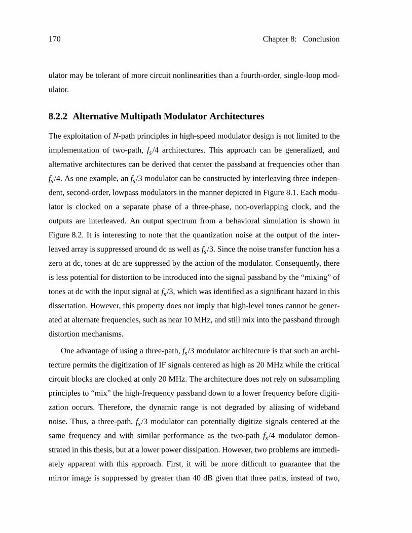
170 Chapter 8: Conclusion
ulator may be tolerant of more circuit nonlinearities than a fourth-order, single-loop mod-
ulator.
8.2.2 Alter native Multipath Modulator Ar chitectures
The exploitation ofN-path principles in high-speed modulator design is not limited to the
implementation of two-path, fs/4 architectures. This approach can be generalized, and
alternative architectures can be derived that center the passband at frequencies other than
fs/4. As one example, anfs/3 modulator can be constructed by interleaving three indepen-
dent, second-order, lowpass modulators in the manner depicted in Figure8.1. Each modu-
lator is clocked on a separate phase of a three-phase, non-overlapping clock, and the
outputs are interleaved. An output spectrum from a behavioral simulation is shown in
Figure8.2. It is interesting to note that the quantization noise at the output of the inter-
leaved array is suppressed around dc as well asfs/3. Since the noise transfer function has a
zero at dc, tones at dc are suppressed by the action of the modulator. Consequently, there
is less potential for distortion to be introduced into the signal passband by the “mixing” of
tones at dc with the input signal atfs/3, which was identified as a significant hazard in this
dissertation. However, this property does not imply that high-level tones cannot be gener-
ated at alternate frequencies, such as near 10 MHz, and still mix into the passband through
distortion mechanisms.
One advantage of using a three-path,fs/3 modulator architecture is that such an archi-
tecture permits the digitization of IF signals centered as high as 20 MHz while the critical
circuit blocks are clocked at only 20MHz. The architecture does not rely on subsampling
principles to “mix” the high-frequency passband down to a lower frequency before digiti-
zation occurs. Therefore, the dynamic range is not degraded by aliasing of wideband
noise. Thus, a three-path,fs/3 modulator can potentially digitize signals centered at the
same frequency and with similar performance as the two-path fs/4 modulator demon-
strated in this thesis, but at a lower power dissipation. However, two problems are immedi-
ately apparent with this approach. First, it will be more difficult to guarantee that the
mirror image is suppressed by greater than 40 dB given that three paths, instead of two,
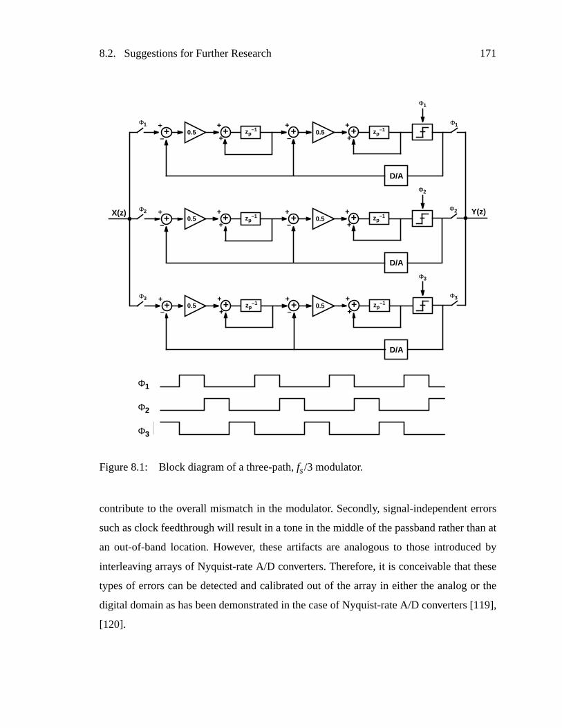
8.2. Suggestions for Further Research 171
contribute to the overall mismatch in the modulator. Secondly, signal-independent errors
such as clock feedthrough will result in a tone in the middle of the passband rather than at
an out-of-band location. However, these artifacts are analogous to those introduced by
interleaving arrays of Nyquist-rate A/D converters. Therefore, it is conceivable that these
types of errors can be detected and calibrated out of the array in either the analog or the
digital domain as has been demonstrated in the case of Nyquist-rate A/D converters [119],
[120].
Figure8.1: Block diagram of a three-path,fs/3 modulator.
Φ1
X(z)
Φ2
Φ1
Φ2
Φ1
Φ2 Y(z)
Φ1
Φ2
0.5 zp–1
zp–10.50.5 zp
–1
0.5 zp–1
D/A
D/A
+
++
+
–+
+
–+
+
++
+
–+
+
–+
+
++
+
++
Φ3
Φ3 Φ3
zp–10.50.5 zp
–1
D/A
+
–+
+
++
+
–+
+
++
Φ3
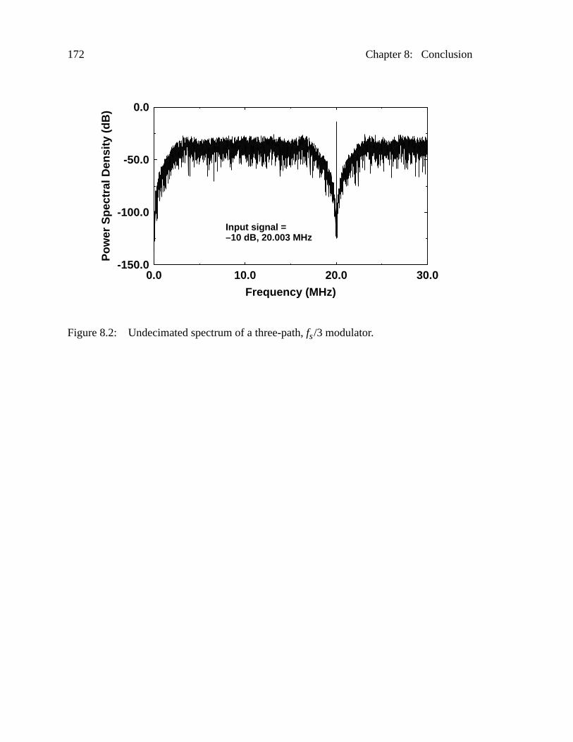
172 Chapter 8: Conclusion
Figure8.2: Undecimated spectrum of a three-path,fs/3 modulator.
0.0 10.0 20.0 30.0-150.0
-100.0
-50.0
0.0
Frequency (MHz)
Pow
er S
pect
ral D
ensi
ty (
dB)
Input signal =–10 dB, 20.003 MHz
173
Appendix A The Design of aFourth-Order, fs/6Modulator
This appendix illustrates the design procedure described in Section3.3.4.2 for synthesiz-
ing a noise transfer function that meets the causality, (3.48), and gain, (3.49), requirements
for an fs/X bandpass modulator. As an example, the design flow is used to design a
fourth-order, fs/6 Butterworth noise transfer function with an out-of-band gain of 1.8.
MATLAB is used extensively to circumvent the tedium associated with the requisite alge-
braic transformations, which map a continuous-time Butterworth filter into thez-domain
by means of the bilinear transform (3.34); the details of this filter design process can be
found in [18].
A.1 Noise Transfer Function Design Flow
In the following steps, the MATLAB butter function is used to design a fourth-order, But-
terworth bandstop filter. Similar methodology can be used to design Chebyshev, elliptical,
or other special classes of discrete-time filters.
(1) Choose the order and the out-of-band gain of the NTF. In this example, the filter is
fourth-order and will have a maximum out-of-band gain of 1.8.
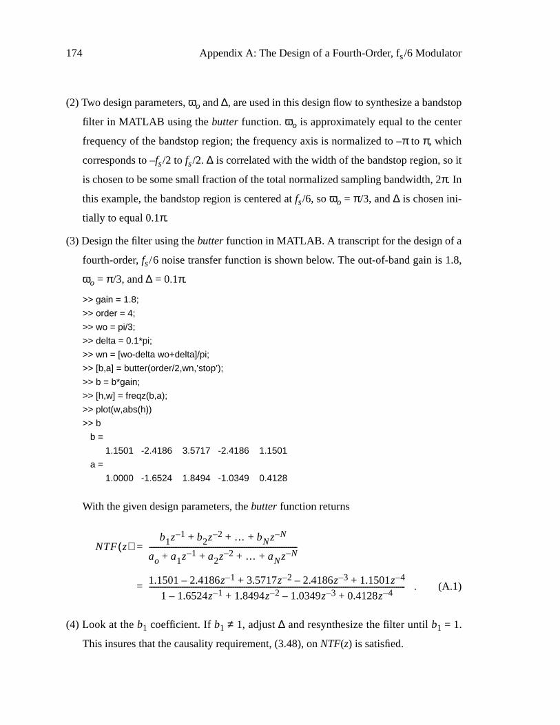
174 Appendix A: The Design of a Fourth-Order, fs/6 Modulator
(2) Two design parameters,ωo and∆, are used in this design flow to synthesize a bandstop
filter in MATLAB using thebutter function.ωo is approximately equal to the center
frequency of the bandstop region; the frequency axis is normalized to –π to π, which
corresponds to –fs/2 to fs/2. ∆ is correlated with the width of the bandstop region, so it
is chosen to be some small fraction of the total normalized sampling bandwidth, 2π. In
this example, the bandstop region is centered atfs/6, soωo = π/3, and∆ is chosen ini-
tially to equal 0.1π.
(3) Design the filter using thebutter function in MATLAB. A transcript for the design of a
fourth-order, fs/6 noise transfer function is shown below. The out-of-band gain is 1.8,
ωo = π/3, and∆ = 0.1π.
With the given design parameters, thebutter function returns
. (A.1)
(4) Look at theb1 coefficient. If b1 ≠ 1, adjust∆ and resynthesize the filter until b1 = 1.
This insures that the causality requirement, (3.48), onNTF(z) is satisfied.
>> gain = 1.8;
>> order = 4;
>> wo = pi/3;
>> delta = 0.1*pi;
>> wn = [wo-delta wo+delta]/pi;
>> [b,a] = butter(order/2,wn,’stop’);
>> b = b*gain;
>> [h,w] = freqz(b,a);
>> plot(w,abs(h))
>> b
b =
1.1501 -2.4186 3.5717 -2.4186 1.1501
a =
1.0000 -1.6524 1.8494 -1.0349 0.4128
NTF z( )b1z 1– b2z 2– … bNz N–+ + +
ao a1z 1– a2z 2– … aNz N–+ + + +---------------------------------------------------------------------------------=
1.1501 2.4186z 1–– 3.5717z 2– 2.4186z 3–– 1.1501z 4–+ +
1 1.6524z 1–– 1.8494z 2– 1.0349z 3–– 0.4128z 4–+ +--------------------------------------------------------------------------------------------------------------------------------------------=
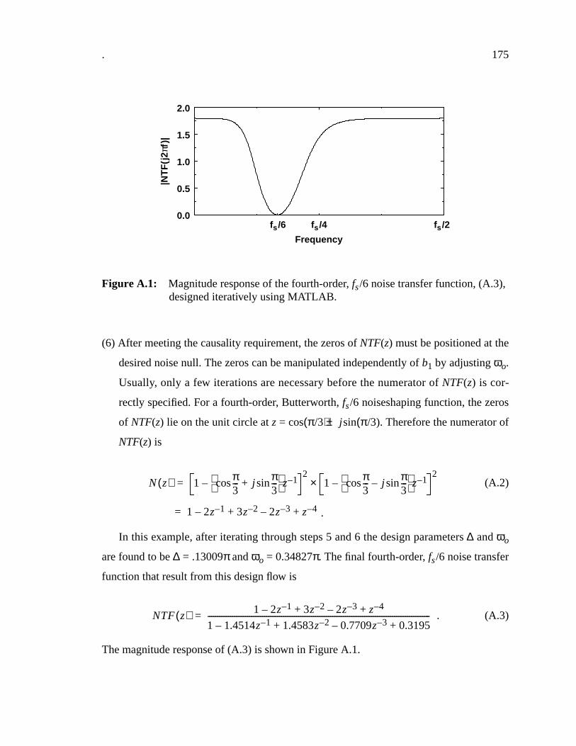
. 175
(6) After meeting the causality requirement, the zeros ofNTF(z) must be positioned at the
desired noise null. The zeros can be manipulated independently ofb1 by adjustingωo.
Usually, only a few iterations are necessary before the numerator ofNTF(z) is cor-
rectly specified. For a fourth-order, Butterworth, fs/6 noiseshaping function, the zeros
of NTF(z) lie on the unit circle atz = cos(π/3) ± jsin(π/3). Therefore the numerator of
NTF(z) is
(A.2)
In this example, after iterating through steps 5 and 6 the design parameters∆ andωo
are found to be∆ = .13009π andωo = 0.34827π. The final fourth-order, fs/6 noise transfer
function that result from this design flow is
. (A.3)
The magnitude response of (A.3) is shown in FigureA.1.
N z( ) 1 π3--- j
π3---sin+cos
z 1––2
1 π3--- j
π3---sin–cos
z 1––2
×=
1 2z 1–– 3z 2– 2z 3–– z 4–+ += .
NTF z( ) 1 2z 1–– 3z 2– 2z 3–– z 4–+ +
1 1.4514z 1–– 1.4583z 2– 0.7709z 3–– 0.3195+ +----------------------------------------------------------------------------------------------------------------------=
0.0
0.5
1.0
1.5
2.0
fs /4 fs /2fs /6
|NT
F(j
2πf
)|
Frequency
Figure A.1: Magnitude response of the fourth-order, fs/6 noise transfer function, (A.3),designed iteratively using MATLAB.
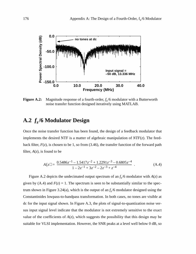
176 Appendix A: The Design of a Fourth-Order, fs/6 Modulator
A.2 fs/6 Modulator Design
Once the noise transfer function has been found, the design of a feedback modulator that
implements the desired NTF is a matter of algebraic manipulation ofNTF(z). The feed-
back filter, F(z), is chosen to be 1, so from (3.46), the transfer function of the forward path
filter, A(z), is found to be
. (A.4)
FigureA.2 depicts the undecimated output spectrum of anfs/6 modulator withA(z) as
given by (A.4) andF(z) = 1. The spectrum is seen to be substantially similar to the spec-
trum shown in Figure3.24(a), which is the output of anfs/6 modulator designed using the
Constantinides lowpass-to-bandpass transformation. In both cases, no tones are visible at
dc for the input signal shown. In FigureA.3, the plots of signal-to-quantization noise ver-
sus input signal level indicate that the modulator is not extremely sensitive to the exact
value of the coefficients ofA(z), which suggests the possibility that this design may be
suitable for VLSI implementation. However, the SNR peaks at a level well below 0 dB, so
A z( ) 0.5486z 1– 1.5417z 2–– 1.2291z 3– 0.6805z 4––+
1 2z 1–– 3z 2– 2z 3–– z 4–+ +---------------------------------------------------------------------------------------------------------------------=
0.0 10.0 20.0 30.0 40.0-150.0
-100.0
-50.0
0.0
Frequency (MHz)
Input signal =–50 dB, 13.336 MHz
Pow
er S
pect
ral D
ensi
ty (
dB)
Figure A.2: Magnitude response of a fourth-order, fs/6 modulator with a Butterworthnoise transfer function designed iteratively using MATLAB.
no tones at dc
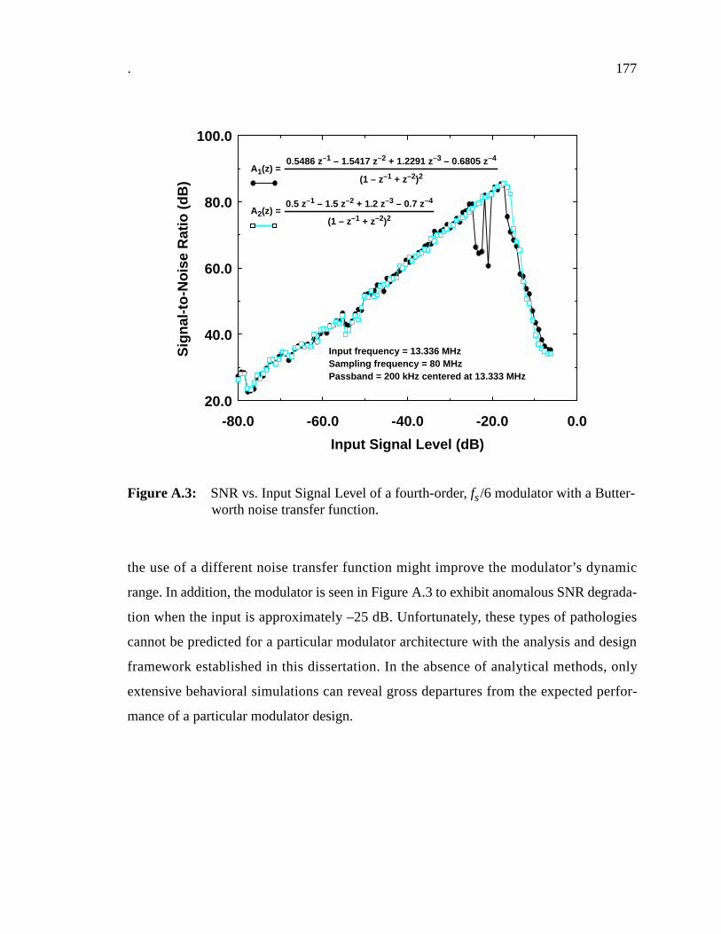
. 177
the use of a different noise transfer function might improve the modulator’s dynamic
range. In addition, the modulator is seen in FigureA.3 to exhibit anomalous SNR degrada-
tion when the input is approximately –25 dB. Unfortunately, these types of pathologies
cannot be predicted for a particular modulator architecture with the analysis and design
framework established in this dissertation. In the absence of analytical methods, only
extensive behavioral simulations can reveal gross departures from the expected perfor-
mance of a particular modulator design.
Figure A.3: SNR vs. Input Signal Level of a fourth-order, fs/6 modulator with a Butter-worth noise transfer function.
Input Signal Level (dB)
Sig
nal-t
o-N
oise
Rat
io (
dB)
-80.0 -60.0 -40.0 -20.0 0.020.0
40.0
60.0
80.0
100.0
0.5486 z–1 – 1.5417 z–2 + 1.2291 z–3 – 0.6805 z–4
(1 – z–1 + z–2)2
0.5 z–1 – 1.5 z–2 + 1.2 z–3 – 0.7 z–4
(1 – z–1 + z–2)2
A1(z) =
A2(z) =
Input frequency = 13.336 MHzSampling frequency = 80 MHzPassband = 200 kHz centered at 13.333 MHz

178 Appendix A: The Design of a Fourth-Order, fs/6 Modulator
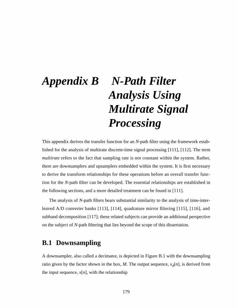
179
Appendix B N-Path FilterAnalysis UsingMultirate SignalProcessing
This appendix derives the transfer function for anN-path filter using the framework estab-
lished for the analysis of multirate discrete-time signal processing [111], [112]. The term
multirate refers to the fact that sampling rate is not constant within the system. Rather,
there are downsamplers and upsamplers embedded within the system. It is first necessary
to derive the transform relationships for these operations before an overall transfer func-
tion for theN-path filter can be developed. The essential relationships are established in
the following sections, and a more detailed treatment can be found in [111].
The analysis ofN-path filters bears substantial similarity to the analysis of time-inter-
leaved A/D converter banks [113], [114], quadrature mirror filtering [115], [116], and
subband decomposition [117]; these related subjects can provide an additional perspective
on the subject ofN-path filtering that lies beyond the scope of this dissertation.
B.1 Downsampling
A downsampler, also called a decimator, is depicted in FigureB.1 with the downsampling
ratio given by the factor shown in the box,M. The output sequence,xd[n], is derived from
the input sequence,x[n], with the relationship
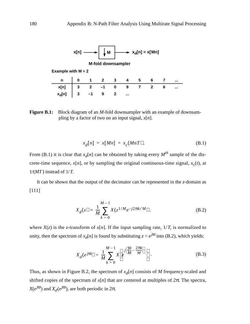
180 Appendix B: N-Path Filter Analysis Using Multirate Signal Processing
. (B.1)
From (B.1) it is clear thatxd[n] can be obtained by taking every Mth sample of the dis-
crete-time sequence,x[n], or by sampling the original continuous-time signal,xc(t), at
1/(MT ) instead of 1/T.
It can be shown that the output of the decimator can be represented in thez-domain as
[111]
. (B.2)
whereX(z) is thez-transform ofx[n]. If the input sampling rate, 1/T, is normalized to
unity, then the spectrum ofxd[n] is found by substitutingz = ejω into (B.2), which yields:
. (B.3)
Thus, as shown in FigureB.2, the spectrum ofxd[n] consists ofM frequency-scaled and
shifted copies of the spectrum ofx[n] that are centered at multiples of 2π. The spectra,
X(ejω) andXd(ejω), are both periodic in 2π.
Figure B.1: Block diagram of anM-fold downsampler with an example of downsam-pling by a factor of two on an input signal,x[n].
Mx[n] xd[n] = x[ Mn]
Example with M = 2
n 0 1 2 3 4 5 6 7 ...
x[n] 3 2 –1 0 9 7 2 6 ...
xd[n] 3 –1 9 2 ...
M-fold downsampler
xd n[ ] x Mn[ ] xc MnT( )= =
Xd z( ) 1M----- X z1 M/ e j2πk– M⁄( )
k 0=
M 1–
∑=
Xd ejω( ) 1M----- X e
jωM----- 2πk
M---------–
k 0=
M 1–
∑=
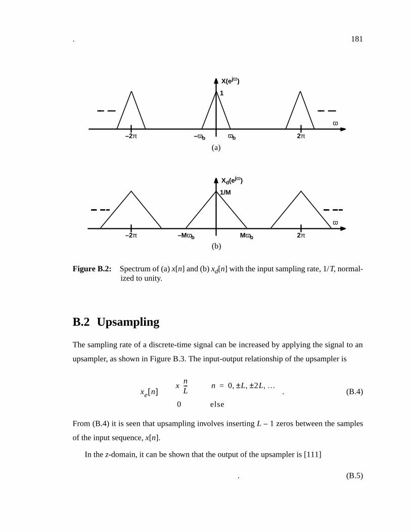
. 181
B.2 Upsampling
The sampling rate of a discrete-time signal can be increased by applying the signal to an
upsampler, as shown in FigureB.3. The input-output relationship of the upsampler is
. (B.4)
From (B.4) it is seen that upsampling involves insertingL – 1 zeros between the samples
of the input sequence,x[n].
In thez-domain, it can be shown that the output of the upsampler is [111]
. (B.5)
Figure B.2: Spectrum of (a)x[n] and (b)xd[n] with the input sampling rate, 1/T, normal-ized to unity.
2π–2π
X(ejω)
ω
ωb–ωb
1
2π–2π
Xd(ejω)
ω
Mωb–Mωb
1/M
(a)
(b)
xe n[ ]x
nL--- n 0 L± 2L± …, , ,=
0 elseî
=
Xe z( ) X zL( )=
182 Appendix B: N-Path Filter Analysis Using Multirate Signal Processing
Once again, normalizing the input sampling rate, 1/T, to unity, the frequency spectrum of
the interpolated signal,xe[n], is found by substitutingz = ejω into (B.5):
. (B.6)
The effect of interpolation in the frequency domain is to compress the original frequency
spectrum ofX(ejω) from (–π, π) to (–π/L, π/L) as illustrated in FigureB.4. As a conse-
quence, the spectrum of the interpolated signal,Xe(ejω), containsL – 1 frequency-scaled
replicas of the basic prototype spectrum,X(ejω), between –π andπ. This frequency com-
pression is a dual of the aliasing property exhibited by downsamplers.
B.3 N-Path Filter Analysis
With the principles of downsampling and upsampling established in the previous two sec-
tions, theN-path filter shown in Figure5.1 and repeated in FigureB.5(a) can be
represented as a multirate discrete-time system, as shown in FigureB.5(b). Recall that in
FigureB.5(a),zp corresponds to thez variable of a single path;zp–1 is interpreted as a sin-
gle delay with respect to the path sampling rate. However, in FigureB.5(b), the interleaved
Figure B.3: Block diagram of anL-fold upsampler with an example of upsampling by afactor of two on an input signal,x[n].
Lx[n]
Example with L = 2
n 0 1 2 3 4 5 6 7 ...
x[n] 3 2 –1 0 9 7 2 6 ...
xe[n] 3 0 2 0 –1 0 9 0 ...
L-fold upsampler
xe n[ ]x n
L--- n 0 L± 2L± …, , ,=
0 elseî
=
Xe ejω( ) X ejωL( )=
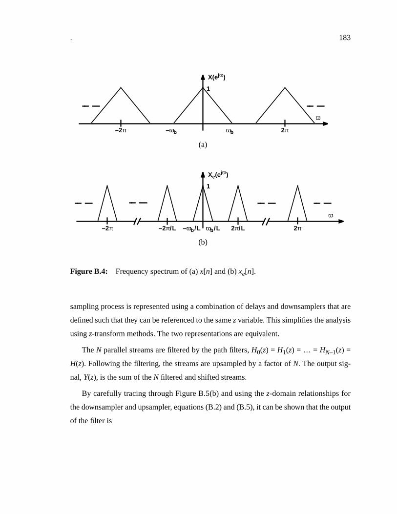
. 183
sampling process is represented using a combination of delays and downsamplers that are
defined such that they can be referenced to the samez variable. This simplifies the analysis
usingz-transform methods. The two representations are equivalent.
TheN parallel streams are filtered by the path filters, H0(z) = H1(z) = … = HN–1(z) =
H(z). Following the filtering, the streams are upsampled by a factor ofN. The output sig-
nal,Y(z), is the sum of theN filtered and shifted streams.
By carefully tracing through FigureB.5(b) and using thez-domain relationships for
the downsampler and upsampler, equations (B.2) and (B.5), it can be shown that the output
of the filter is
Figure B.4: Frequency spectrum of (a)x[n] and (b)xe[n].
2π–2π
Xe(ejω)
ω
ωb /L–ωb /L
1
2π–2π
X(ejω)
ω
ωb–ωb
1
2π/L–2π/L
(a)
(b)
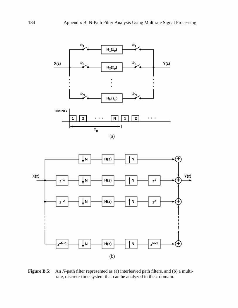
184 Appendix B: N-Path Filter Analysis Using Multirate Signal Processing
N NH(z)
N NH(z)z–1 z1
N NH(z)z–2 z2
N NH(z)z–N+1 zN–1
X(z) Y(z)
+
+
+
+
H1(zp)
H2(zp)
HN(zp)
X(z) Y(z)
1 2 N 1 2
Tp
TIMING
Φ1 Φ1
Φ2 Φ2
ΦN ΦN
(a)
(b)
Figure B.5: An N-path filter represented as (a) interleaved path filters, and (b) a multi-rate, discrete-time system that can be analyzed in thez-domain.
. 185
(B.7)
This expression can be written more compactly as
. (B.8)
Interchanging the summations with respect tok andm leads to
, (B.9)
which can be separated as
(B.10)
Finally, making use of the relationship
, (B.11)
it is found that
(B.12)
which is precisely the result stated in equation (5.1).
Y z( ) H zN( )N
---------------- X ze j2πk N⁄–( )k 0=
N 1–
∑ H zN( )N
---------------- ej2πk N⁄ X ze j2πk N⁄–( )k 0=
N 1–
∑ …+ +=
H zN( )N
---------------- ej2πk
N 1–N
-------------X ze j2πk N⁄–( )
k 0=
N 1–
∑+ .
Y z( ) H zN( )N
---------------- ej2πkm N⁄ X ze j2πk N⁄–( )k 0=
N 1–
∑m 0=
N 1–
∑=
Y z( ) H zN( )N
---------------- ej2πkm N⁄ X ze j2πk N⁄–( )m 0=
N 1–
∑k 0=
N 1–
∑=
Y z( ) H zN( )N
---------------- X ze j2πk N⁄–( ) ej2πkm N⁄
m 0=
N 1–
∑k 0=
N 1–
∑=
ej2πkm N⁄
m 0=
N 1–
∑ N k 0 N± 2N± …, , ,=
0 elseî
=
Y z( ) H zN( )N
---------------- X ze j2π0 N⁄–( ) N⋅[ ]=
H zN( ) X z( )= ,

186 Appendix B: N-Path Filter Analysis Using Multirate Signal Processing
187
Bibliography
[1] “Universal Personal Communications,” Press Service, InternationalTelecommunication Union, Geneva, Switzerland.
[2] D. C. Cox, “Universal digital portable radio communications,” Proc. IEEE, vol.75, no. 4, pp. 436-476, April 1987.
[3] A. J. Viterbi, “The evolution of digital wireless technology from space explorationto personal communication services,” IEEE Trans. Vehicular Tech., vol. 43, no. 3,pp. 638-644, August 1994.
[4] B. Razavi, RF Microelectronics. New Jersey: Prentice-Hall, 1998.
[5] EIA/TIA Interim Standard, “Recommended minimum performance standard for800 MHz dual mode mobile stations,” EIA/TIA/IS-55, December 1991.
[6] J. Y. C. Cheah, “Introduction to wireless communications applications and circuitdesign,” in RF and Microwave Circuit Design for Wireless Communications, ed.L. E. Larson, Boston: Artech House, pp. 17-41, 1997.
[7] T. H. Lee,The Design of CMOS Radio-Frequency Integrated Circuits. Cambridge:Cambridge University Press, 1998.
[8] V. Eerola, H. Lampinen, T. Ritoniemi, and H. Tenhunen, “Direct conversion usinglowpass sigma-delta modulation,” Proc. 1992 IEEE Int. Symp. Circuits Syst.,pp.2653-2656, May 1992.
188 Bibliography
[9] C. C. Cutler, “Transmission system employing quantization,” U.S. Patent No.2,927,962, March 8, 1960 (filed 1954).
[10] H. Inose, Y. Yasuda, and J. Murakami, “A telemetering system by code modulation– Σ∆ modulation,” IRE Trans. Space Electron. Telem., vol. SET-8, pp. 204-209,September 1962. (reprinted in N. S. Jayant, Ed.,Waveform Quantization andCoding, IEEE Press, New York, 1976.)
[11] H. Inose and Y. Yasuda, “A unity bit coding method by negative feedback,” Proc.IEEE, vol. 51, pp. 1524-1535, November 1963.
[12] R. J. van de Plassche, “A sigma-delta modulator as an A/D converter,” IEEE Trans.Circuits Syst., vol. CAS-25, no. 7, pp. 510-514, July 1978.
[13] J. C. Candy, “A use of double integration in sigma delta modulation,” IEEE Trans.on Comm., vol. COM-33, pp. 249-258, March 1985.
[14] B. E. Boser and B. A. Wooley, “The design of sigma-delta modulationanalog-to-digital converters,” IEEE J. Solid-State Circuits, vol. 23, no. 6, pp.1298-1308, December 1988.
[15] A. R. Feldman, B. E. Boser, and P. R. Gray, “A 13 bit, 1.4 MS/s, 3.3 V sigma-deltamodulator for RF baseband channel applications,” Proc. 1998 IEEE CustomIntegrated Circuits Conference, pp.229-232, May1998.
[16] R. Schreier and W. M. Snelgrove, “Bandpass sigma-delta modulation,” Electron.Lett., vol 25, no. 23, pp. 1560-1561, November 1989.
[17] S. Jantzi, R. Schreier, and M. Snelgrove, “Bandpass sigma-delta analog-to-digitalconversion,” IEEE Trans. Circuits Syst., vol. 38, no. 11, pp. 1406-1409, November1991.
[18] A. V. Oppenheim and R. W. Schafer, Discrete-Time Signal Processing, NewJersey: Prentice Hall, 1989.
[19] W. Bennett, “Spectra of quantized signals,” Bell System Tech. Journal, vol.BSTJ-27, pp. 446-472, 1948.
[20] B. Widrow, “A study of rough amplitude quantization by means of Nyquistsampling theory,” IRE Trans. Circuit Theory, vol. CT-3, pp. 266-276, December1956.
[21] R. M. Gray, “Quantization noise spectra,” IEEE Trans. Inform. Theory, vol. 36, no.6, pp. 1220-1244, November 1990.
Bibliography 189
[22] R. van de Plassche,Integrated Analog-to-Digital and Digital-to-AnalogConverters,Boston: Kluwer Academic Publishers, 1994.
[23] B. Razavi, Principles of Data Conversion System Design,New Jersey: IEEE Press,1995.
[24] V. Gopinathan, Y. P. Tsividis, K.-S. Tan, and R. K. Hester, “Design considerationsfor high-frequency continuous-time filters and implementation of an antialiasingfilter for digital video,” IEEE J. Solid-State Circuits, vol. 25, no. 6, pp. 1368-1378,December 1990.
[25] Y.-T. Wang and A. A. Abidi, “CMOS active filter design at very high frequencies,”IEEE J. Solid-State Circuits, vol. 25, no. 6, pp. 1562-1573, December 1990.
[26] B. Nauta, “A CMOS transconductance-C filter technique for very highfrequencies,” IEEE J. Solid-State Circuits, vol. 27, no. 2, pp. 142-153, February1992.
[27] Y. P. Tsividis, “Integrated continuous-time filter design – an overview,” IEEE J.Solid-State Circuits, vol. 29, no. 3, pp. 166-176, March 1994.
[28] S. D. Willingham, K. W. Martin, and A. Ganesan, “A BiCMOS low-distortion8-MHz low-pass filter,” IEEE J. Solid-State Circuits, vol. 28, no. 12, pp.1234-1245, December 1993.
[29] K. Halonen, S. Lindfors, J. Jussila, and L. Siren, “A 3V gmC-filter with on-chiptuning for CDMA,” Proc. 1997 IEEE Custom Integrated Circuits Conference,pp.83-86, May1997.
[30] D. J. Allstot and W. C. Black, Jr., “Technological design considerations formonolithic MOS switched-capacitor filtering systems,” Proc. IEEE, vol. 71, no. 8,pp. 967-986, August 1983.
[31] F. de Jager, “Delta modulation, a method of PCM transmission using the 1-unitcode,” Philips Res. Rep., vol. 7, pp. 442-466, 1952.
[32] A. Tomozawa and H. Kaneko, “Companded delta modulation for telephonetransmission,” IEEE Trans. Comm. Tech., vol. COM-16, February 1968.
[33] J. Greefkes and F. de Jager, “Continuous delta modulation,” Philips Res. Rep., vol.23, 1968.
[34] D. J. Goodman, “The application of delta modulation to analog-to-PCMencoding,” Bell System Tech. Journal, vol. 48, pp. 321-343, February 1969.
190 Bibliography
[35] M. W. Hauser, “Principles of oversampling A/D conversion,” J. Audio Eng. Soc.,vol. 39, no. 1/2, pp. 3-26, January/February 1991.
[36] B. Leung, “Theory ofΣ–∆ analog to digital converter,” IEEE ISCAS ‘94 Tutorials,pp. 196-223, 1994.
[37] P. M. Aziz, H. V. Sorensen, and J. van der Spiegel, “An overview of sigma-deltaconverters,” IEEE Signal Proc. Mag., pp. 61-84, January 1996.
[38] J. J. Paulos, G. T. Brauns, M. B. Steer, S. H. Ardalan, “Improved signal-to-noiseratio using trilevel delta-sigma modulation,” Proc. 1987 IEEE Int. Symp. CircuitsSyst., pp. 463-466, May 1987.
[39] B. P. Brandt and B. A. Wooley, “A 50-MHz multibit sigma-delta modulator for12-b, 2-MHz A/D conversion,” IEEE J. Solid-State Circuits, vol. 26, pp.1746-1756, December 1991.
[40] P. Ju, K. Suyama, P. F. Ferguson, Jr., and W. Lee, “A 22-kHz multibitswitched-capacitor sigma-delta D/A converter with 92 dB dynamic range,” IEEE J.Solid-State Circuits, vol. 30, no. 12, pp. 1316-1325, December 1995.
[41] K. Y. Leung, E. J. Swanson, K. Leung, and S. S. Zhu, “A 5V, 118dB DSanalog-to-digital converter for wideband digital audio,” ISSCC Digest of Tech.Papers, pp. 218-219, February 1997.
[42] L. R. Carley, “A noise-shaping coder topology for 15+ bit converters,” IEEE J.Solid-State Circuits, vol. 24, no. 2, pp. 267-273, April 1989.
[43] F. Chen and B. H. Leung, “A high resolution multibit sigma-delta modulator withindividual level averaging,” IEEE J. Solid-State Circuits, vol. 30, no. 4, pp.453-460, April 1995.
[44] I. Galton and P. Carbone, “A rigorous error analysis of D/A conversion withdynamic element matching,” IEEE Trans. Circuits Syst. II: Analog Dig. Sig. Proc.,vol. 42, no. 12, pp. 763-772, December 1995.
[45] K. C.-H. Chao, S. Nadeem, W. L. Lee, and C. G. Sodini, “A higher order topologyfor interpolative modulators for oversampling A/D converters,” IEEE Trans.Circuits Syst., vol. CAS-37, no. 3, pp. 309-318, March 1990.
[46] R. W. Adams, P. F. Ferguson, Jr., A. Ganesan, S. Vincelette, A. Volpe, and R.Libert, “Theory and practical implementation of a fifth-order sigma-delta A/Dconverter,” J. Audio Eng. Soc., vol. 39, no. 7-8, pp. 515-528, July-August 1991.
Bibliography 191
[47] R. Schreier, “An empirical study of high-order single-bit delta-sigma modulators,”IEEE Trans. Circuits Syst. II: Analog Dig. Sig. Proc., vol. 40, no. 8, pp. 461-6,August 1993.
[48] S. M. Moussavi and B. H. Leung, “High-order single-stage single-bitoversampling A/D converter stabilized with local feedback loops,” IEEE Trans.Circuits Syst. II: Analog Dig. Sig. Proc., vol. 41, no. 1, pp. 19-25, January 1994.
[49] L. A. Williams, III, and B. A. Wooley, “A third-order sigma-delta modulator withextended dynamic range,” IEEE J. Solid-State Circuits, vol. 29, no. 3, pp. 193-202,March 1994.
[50] S. A. Jantzi, K. A. Martin, and A. S. Sedra, “Quadrature bandpassΣ∆ modulationfor digital radio,” IEEE J. Solid-State Circuits, vol. 32, no. 12, pp. 1935-1950,December 1997.
[51] T. Paulus, S. Somayajula, T. Miller, K. Choi, B. Trotter, and D. Kerth, “A CMOSIF transceiver for narrowband PCS,” ISSCC Digest of Tech. Papers, pp. 46-47,February 1998.
[52] E. J. van der Zwan and E. C. Dijkmans, “A 0.2-mW CMOSΣ∆ modulator forspeech coding with 80 dB dynamic range,” IEEE J. Solid-State Circuits, vol. 31,no. 12, pp. 1873-1880, December 1996.
[53] S. R. Norsworthy, “Quantization errors and dithering in∆Σ modulation,” inDelta-Sigma Data Converters: Theory, Design, and Simulation, ed. S. R.Norsworthy, R. Schreier, and G. C. Temes, New York: IEEE Press, 1996.
[54] A. K. Ong and B. A. Wooley, A two-path bandpassΣ∆ modulator for digital IFextraction at 20 MHz,” IEEE J. Solid-State Circuits, vol. 32, no. 12, pp.1920-1934, December 1997.
[55] L. Longo and B.-R. Horng, “A 15b 30kHz bandpass sigma-delta modulator,”ISSCC Digest of Tech. Papers, pp. 226-227, February 1993.
[56] B.-S. Song, “A fourth-order bandpass delta-sigma modulator with reduced numberof op amps,” IEEE J. Solid-State Circuits, vol. 30, no. 12, pp. 1309-1315,December 1995.
[57] B. P. Brandt,Oversampled Analog-to-Digital Conversion, Ph.D. thesis, StanfordUniversity, August 1991.
[58] A. Antoniou,Digital Filters: Analysis, Design, and Applications, San Francisco:McGraw-Hill, 1993.
192 Bibliography
[59] R. N. Bracewell, The Fourier Transform and Its Applications, San Francisco:McGraw-Hill, p. 217, 1986.
[60] R. G. Vaughan, N. L. Scott, and D. R. White, “The theory of bandpass sampling,”IEEE Trans. Signal Proc., vol. 39, no. 9, pp. 1973-1984, September 1991.
[61] L. A. Williams, III, and B. A. Wooley, “MIDAS - a functional simulator for mixeddigital and analog sampled data systems,” Proc. 1992 IEEE Int. Symp. CircuitsSyst., pp. 2148-2151, May 1992.
[62] A.G. Constantinides, “Spectral transformations for digital filters,” Proc. IEE,vol. 117, no.8, pp. 1585-90, Aug. 1970.
[63] D. H. Horrocks, “A second-order oversampled sigma-delta modulator for bandpasssignals,” Proc. 1991 IEEE Int. Symp. Circuits Syst., pp. 1653-1656, June 1991, pp.1653-1656.
[64] S. Jantzi, C. Ouslis, and A. Sedra, “Transfer function design for∆Σ converters,”Proc. 1994 IEEE Int. Symp. Circuits Syst., pp. 433-436, June 1994.
[65] P. F. Ferguson, Jr., A. Ganesan, and R. W. Adams, “One bit higher ordersigma-delta A/D converters,” Proc. 1990 IEEE Int. Symp. Circuits Syst., pp.890-893, May 1990.
[66] G. Tröster, H.-J. Dreßler, H.-J. Golberg, W. Schardein, E. Zocher, A. Wedel, K.Schoppe, and J. Arndt, “An interpolative bandpass converter on a 1.2-µm BiCMOSAnalog/Digital Array,” IEEE J. Solid-State Circuits, vol. 28, no. 4, pp. 471-477,April 1993.
[67] F. W. Snelgrove and W. M. Snelgrove, “Switched-capacitor bandpass delta-sigmaA/D modulation at 10.7 MHz,” IEEE J. Solid-State Circuits, vol. 30, no. 3, pp.184-192, March 1995.
[68] L. Vogt, D. Brookshire, S. Lottholz, and G. Zwiehoff, “A two-chip digital carradio,” ISSCC Digest of Tech. Papers, pp. 350-351, February 1996.
[69] A. Hairapetian, “An 81-MHz IF receiver in CMOS,” IEEE J. Solid-State Circuits,vol. 31, no. 12, pp. 1981-1986, December 1996.
[70] F. Francesconi, V. Liberali, and F. Maloberti, “A 10.7 MHz N-path fourth-orderbandpass sigma-delta modulator,” Proc. 1996 ESSIRC, pp. 216-219, September1996.
Bibliography 193
[71] S. Chuang, X. Yu, T. L. Sculley, and R. H. Bamberger, “Design andimplementation of a sixth order bandpass delta-sigma A/D converter with singlequantizer,” Proc. 1997 IEEE Int. Symp. Circuits Syst., pp. 381-384, June 1997.
[72] A. B. Carlson,Communication Systems. San Francisco: McGraw-Hill, 1986.
[73] A. Sedra and G. Roberts, “Sampled-data analog filters,” in Analog VLSI: Signaland Information Processing, ed. M. Ismail and T. Fiez, San Francisco:McGraw-Hill, pp. 414-466, 1994.
[74] D. H. Shen,Architecture and Design of a Monolithic Radio Frequency Receiver,Ph.D. Dissertation, Stanford University, March 1997.
[75] R. M. Gray and L. D. Davisson,Random Processes: A Mathematical Approach forEngineers, New Jersey: Prentice Hall, 1986.
[76] A. Hajimiri and T. H. Lee, “A general theory of phase noise in electricaloscillators,” IEEE J. Solid-State Circuits, vol. 33, no. 2, pp. 179-194, February1998.
[77] K. Martin and A. S. Sedra, “Effects of the op amp finite gain and bandwidth on theperformance of switched-capacitor filters,” IEEE Trans. Circuits Syst., vol.CAS-28, no. 8, pp. 822-829, August 1981.
[78] D. B. Ribner and M. A. Copeland, “Biquad alternatives for high-frequencyswitched-capacitor filters,” IEEE J. Solid-State Circuits, vol. SC-20, no. 6, pp.1085-1095, December 1985.
[79] S. Rabii and B. A. Wooley, “A 1.8-V digital-audio sigma-delta modulator in0.8-µm CMOS,” IEEE J. Solid-State Circuits, vol. 32, no. 6, pp. 783-796, June1997.
[80] L. E. Franks and I. W. Sandberg, “An alternative approach to the realization ofnetwork transfer functions: theN-path filter,” Bell Syst. Tech. J., vol. 39, pp.1321-1350, September 1960.
[81] A. Acampora, “The generalized transfer function and pole-zero migrations inswitched networks,” RCA Rev., vol. 27, no. 2, pp. 245-262, June 1966.
[82] A. G. J. Holt and C. Pulé, “Switched high-pass RC filters,” Int. J. Electronics, vol.28, no. 5, pp. 449-457, 1970.
194 Bibliography
[83] D. C. Von Grünigen, R. P. Sigg, J. Schmid, G. S. Moschytz, and H. Melchior, “Anintegrated CMOS switched-capacitor bandpass filter based onN-path andfrequency-sampling principles,” IEEE J. Solid-State Circuits, vol. SC-18, no. 6,pp. 753-761, December 1983.
[84] S. K. Berg and P. J. Hurst, “An 80-Msample/s video switched-capacitor filter usinga parallel biquadratic structure,” IEEE J. Solid-State Circuits, vol. 30, no. 8, pp.898-905, August 1995.
[85] R. Gregorian and G. Temes,Analog MOS Integrated Circuits. New York: Wiley,1986.
[86] Y.-C. Jenq, “Digital spectra of nonuniformly sampled signals: fundamentals andhigh-speed waveform digitizers,” IEEE Trans. Instrum. Meas., vol. 37, no. 2, pp.245-251, June 1988.
[87] A. Petraglia and S. K. Mitra, “Analysis of mismatch effects among A/D convertersin a time-interleaved waveform digitizer,” IEEE Trans. Instrum. Meas., vol. 40, no.5, pp. 831-835, October 1991.
[88] R. Khoini-Poorfard and D. A. Johns, “Mismatch effects in time-interleavedoversampling converters,” Proc. 1994 IEEE Int. Symp. Circuits Syst., pp. 429-432,May 1994.
[89] J. Crols and M. S. J. Steyaert, “A single-chip 900 MHz CMOS receiver front-endwith a high performance low-IF topology,” IEEE J. Solid-State Circuits, vol. 30,no. 12, pp. 1483-1492, December 1995.
[90] J. W. Archer, J. Granlund, and R. E. Mauzy, “A broad-band UHF mixer exhibitinghigh image rejection over a multidecade baseband frequency range,” IEEE J.Solid-State Circuits, vol. SC-16, no. 4, pp. 385-392, August 1981.
[91] T. D. Stetzler, I. G. Post, J. J. Havens, and M. Koyama, “A 2.7–4.5 V single chipGSM transceiver RF integrated circuit,” IEEE J. Solid-State Circuits, vol. 30, no.12, pp. 1421-1428, December 1995.
[92] A. Montijo and K. Rush, “Accuracy in interleaved ADC systems,”Hewlett-Packard Journal,vol. 44, no. 5, pp. 38-46, October 1993.
[93] K.-C. Hsieh, P. R. Gray, D. Senderowicz, and D. G. Messerschmitt, “A low-noisechopped-stabilized differential switched-capacitor filtering technique,” IEEE J.Solid-State Circuits, vol. SC-16, no. 6, pp. 708-715, December 1981.
Bibliography 195
[94] K.-L. Lee and R. G. Meyer, “Low-distortion switched-capacitor filter designtechniques,” IEEE J. Solid-State Circuits, vol. SC-20, no. 6, pp. 1103-1112,December 1985.
[95] P. R. Gray and R.G. Meyer, Analysis and Design of Analog Integrated Circuits,2nd ed., John Wiley & Sons, New York, 1993, pp. 710-721
[96] J. H. Fischer, “Noise sources and calculation techniques for switched capacitorfilters,” IEEE J. Solid State Circuits, vol. SC-17, pp. 742-752, August 1982.
[97] C.-A. Gobet and A. Knob, “Noise analysis of switched capacitor networks,” IEEETrans. Circuits Syst., vol. CAS-30, pp. 37-43, January. 1983.
[98] S. Rabii, Design of Low-Voltage, Low-Power Sigma-Delta Modulators, Ph.D.thesis, Stanford University, May 1998.
[99] A. A. Abidi, “High-frequency noise measurements on FET’s with smalldimensions,” IEEE Trans. on Electron Devices, vol. ED-33, no. 11, pp. 1801-1805, November 1986.
[100] D. K. Shaeffer and T. H. Lee, “A 1.5-V, 1.5-GHz CMOS low noise amplifier,”IEEE J. Solid State Circuits, vol. 32, no. 5, pp. 745-759, May 1987.
[101] J. N. Babanezhad and R. Gregorian, “A programmable gain/loss circuit,” IEEE J.Solid-State Circuits, vol. SC-22, no. 6, pp. 1082-1089, December 1987.
[102] K. A. Nishimura and P. R. Gray, “A monolithic analog video comb filter in 1.2-µmCMOS,” IEEE J. Solid-State Circuits, vol. 28, no. 12, pp. 1331-1339, December1993.
[103] T. B. Cho and P. R. Gray, “A 10 b, 20 Msample/s, 35 mW pipeline A/D converter,”IEEE J. Solid-State Circuits, vol. 30, no. 3, pp. 166-172, March 1995.
[104] L. A. Williams, III., Modeling and Design of High-Resolution Sigma-DeltaModulators, Ph.D. thesis, Stanford University, August 1993.
[105] L. R. Carley. “Analog layout challenges,” in Analog VLSI: Signal and InformationProcessing, ed. M. Ismail and T. Fiez, San Francisco: McGraw-Hill, pp. 677-687,1994.
[106] T. Blalack, Switching Noise in Mixed-Signal Integrated Circuits, Ph.D. thesis,Stanford University, pp. 101-102, December 1997.
196 Bibliography
[107] U. Gatti and F. Maloberti, “Analog and mixed analog-digital layout,” in AnalogVLSI: Signal and Information Processing, ed. M. Ismail and T. Fiez, SanFrancisco: McGraw-Hill, pp. 699-726, 1994.
[108] R. C. J. Taylor, “Switched capacitor filters,” in Analog Circuit Design, ed. J. H.Huijsing, R. J. van de Plassche, and W. M. C. Sansen, Boston: Kluwer AcademicPublishers, pp. 203-225, 1996.
[109] Crystal Semiconductor Corporation Application Note, “Voltage references for theCS5012/CS5014/CS5016/CS5101/CS5102/CS5126 series of A/D converters,”January 1990.
[110] D. O. Pederson,Analog Integrated Circuits for Communication, Boston: KluwerAcademic Publishers, pp. 55-59, 1991.
[111] R. E. Crochiere and L. R. Rabiner, Multirate Digital Signal Processing,Prentice-Hall, Englewood Cliffs, NJ, 1983.
[112] J. Franca, A. Petraglia, and S. K. Mitra, “Multirate analog-digital systems forsignal processing and conversion,” Proc. IEEE, vol. 85, no. 2, pp. 242-262,February 1997.
[113] C. S. G. Conroy, D. W. Cline, and P. R. Gray, “An 8-b 85-MS/s parallel pipeline A/D converter in 1-µm CMOS,” IEEE J. Solid-State Circuits, vol. 28, no. 4, pp.447-454, April 1993.
[114] W. C. Black and D. A. Hodges, “Time-interleaved A/D converter arrays,” IEEE J.Solid-State Circuits, vol. SC-15, no. 6, pp. 1022-1029, December 1980.
[115] P. P. Vaidyanathan, “Quadrature mirror filter banks, m-band extensions, andperfect-reconstruction techniques,” IEEE ASSP Magazine, vol. 4, no. 3, pp. 4-20,July 1987.
[116] A. Petraglia and S. K. Mitra, “High-speed A/D conversion incorporating a QMFbank,” IEEE Trans. Instrum. Meas., vol. 41, no. 3, pp. 427-431, June 1992.
[117] M. Vetterli, “Filter banks allowing perfect reconstruction,” Signal Processing,vol. 10, no. 3, pp. 219-244, April 1986.
[118] D. B. Ribner, “Multistage bandpass delta sigma modulators,” IEEE Trans. CircuitsSyst. II: Analog Dig. Sig. Proc., vol. 41, no. 6, pp. 402-405, June 1994.
[119] D. Fu, K. Dyer, S. Lewis, P. Hurst, “Digital background calibration of a 10b40MSample/s parallel pipelined ADC,” ISSCC Digest of Tech. Papers, pp.140-141, February 1998.

Bibliography 197
[120] K. Dyer, D. Fu, S. Lewis, P. Hurst, “Analog background calibration of a 10b40MSample/s parallel pipelined ADC,” ISSCC Digest of Tech. Papers, pp.142-143, February 1998.