b. van zeghbroeck, 2004 - internet archive
TRANSCRIPT

B. Van Zeghbroeck, 2004
.
http://ece-www.colorado.edu/~bart/book/book/title.htm11/10/2004 16:07:51

Contents
Title Page Table of Contents Help Copyright B. Van Zeghbroeck, 2004
Principles of Semiconductor Devices
Table of Contents
Short table of contents
Title pageTable of contentsCDROM helpCopyright
Introduction
0.1. The semiconductor industry0.2. Purpose and goal of the Text0.3. The primary focus: CMOS integrated circuits0.4. Applications illustrated with computer-generated animations
Chapter 1: Review of Modern Physics
1.1. Introduction
1.2. Quantum mechanics1.2.1. Particle-wave duality1.2.2. The photo-electric effect1.2.3. Blackbody radiation1.2.4. The Bohr model1.2.5. Schrödinger's equation1.2.6. Pauli exclusion principle1.2.7. Electronic configuration of the elements
1.3. Electromagnetic theory1.3.1. Gauss's law1.3.2. Poisson's equation
1.4. Statistical thermodynamics1.4.1. Thermal equilibrium1.4.2. Laws of thermodynamics1.4.3. The thermodynamic identity1.4.4. The Fermi energy1.4.5. Some useful thermodynamics results
http://ece-www.colorado.edu/~bart/book/book/contents.htm (1 of 9)11/10/2004 16:12:47

Contents
Examples- Problems- Review Questions- Bibliography- Glossary - Equations
Chapter 2: Semiconductor fundamentals
2.1. Introduction
2.2. Crystals and crystal structures2.2.1. Bravais lattices2.2.2. Miller indices, crystal planes and directions2.2.3. Common semiconductor crystal structures2.2.4. Growth of semiconductor crystals
2.3. Energy bands2.3.1. Free electron model2.3.2. Periodic potentials2.3.3. Energy bands of semiconductors2.3.4. Metals, insulators and semiconductors2.3.5. Electrons and holes in semiconductors2.3.6. The effective mass concept2.3.7. Detailed description of the effective mass
2.4. Density of states2.4.1. Calculation of the density of states2.4.2. Density of states in 1, 2 and 3 dimensions
2.5. Carrier distribution functions2.5.1. The Fermi-Dirac distribution function2.5.2. Example2.5.3. Impurity distribution functions2.5.4. Other distribution functions and comparison2.5.5. Derivation of the Fermi-Dirac distribution function
2.6. Carrier densities2.6.1. General discussion2.6.2. Calculation of the Fermi integral2.6.3. Intrinsic semiconductors2.6.4. Doped semiconductors2.6.5. Non-equilibrium carrier densities
2.7. Carrier transport2.7.1. Carrier drift2.7.2. Carrier mobility2.7.3. Velocity saturation2.7.4. Carrier diffusion2.7.5. The Hall effect
http://ece-www.colorado.edu/~bart/book/book/contents.htm (2 of 9)11/10/2004 16:12:47
Contents
2.8. Carrier recombination and generation2.8.1. Simple recombination-generation model2.8.2. Band-to-band recombination2.8.3. Trap-assisted recombination2.8.4. Surface recombination2.8.5. Auger recombination2.8.6. Generation due to light2.8.7. Derivation of the trap-assisted recombination
2.9. Continuity equation2.9.1. Derivation2.9.2. The diffusion equation2.9.3. Steady state solution to the diffusion equation
2.10. The drift-diffusion model
2.11 Semiconductor thermodynamics2.11.1. Thermal equilibrium2.11.2. Thermodynamic identity2.11.3. The Fermi energy2.11.4. Example: an ideal electron gas2.11.5. Quasi-Fermi energies2.11.6. Energy loss in recombination processes2.11.7. Thermo-electric effects in semiconductors2.11.8. The thermoelectric cooler2.11.9. The "hot-probe" experiment
Examples- Problems- Review Questions- Bibliography- Glossary - Equations
Chapter 3: Metal-Semiconductor Junctions
3.1. Introduction
3.2. Structure and principle of operation3.2.1. Structure3.2.2. Flatband diagram and built-in potential3.2.3. Thermal equilibrium3.2.4. Forward and reverse bias
3.3. Electrostatic analysis3.3.1. General discussion - Poisson's equation3.3.2. Full depletion approximation3.3.3. Full depletion analysis3.3.4. Junction capacitance3.3.5. Schottky barrier lowering3.3.6. Derivation of Schottky barrier lowering
http://ece-www.colorado.edu/~bart/book/book/contents.htm (3 of 9)11/10/2004 16:12:47

Contents
3.3.7. Solution to Poisson's equation
3.4. Schottky diode current3.4.1. Diffusion current3.4.2. Thermionic emission current3.4.3. Tunneling3.4.4. Derivation of the Metal-Semiconductor junction current
3.5 Metal-Semiconductor contacts3.5.1. Ohmic contacts3.5.2. Tunnel contacts3.5.3. Annealed and alloyed contacts3.5.4. Contact resistance to a thin semiconductor layer
3.6 Metal-Semiconductor Field Effect Transistors (MESFETs)
3.7 Schottky diode with an interfacial layer
3.8 Other unipolar junctions3.8.1. The n-n+ homojunction3.8.2. The n-n+ heterojunction3.8.3. Currents across a n-n+ heterojunction
3.9 Currents through insulators3.9.1. Fowler-Nordheim tunneling3.9.2. Poole-Frenkel emission3.9.3. Space charge limited current3.9.4. Ballistic transport in insulators
Examples- Problems- Review Questions- Bibliography- Glossary - Equations
Chapter 4: p-n Junctions
4.1. Introduction
4.2. Structure and principle of operation4.2.1. Flatband diagram4.2.2. Thermal equilibrium4.2.3. The built-in potential4.2.4. Forward and reverse bias
4.3. Electrostatic analysis of a p-n diode4.3.1. General discussion - Poisson's equation4.3.2. The full-depletion approximation4.3.3. Full depletion analysis4.3.4. Junction capacitance
http://ece-www.colorado.edu/~bart/book/book/contents.htm (4 of 9)11/10/2004 16:12:47
Contents
4.3.5. The linearly graded p-n diode4.3.6. The abrupt p-i-n diode4.3.7. Solution to Poisson's equation4.3.8. The heterojunction p-n diode
4.4. The p-n diode current4.4.1. General discussion4.4.2. The ideal diode current4.4.3. Recombination-generation current4.4.4. I-V characteristics of real p-n diodes4.4.5. The diffusion capacitance4.4.6. High injection effects4.4.7. p-n heterojunction current
4.5. Reverse bias breakdown4.5.1. General breakdown characteristics4.5.2. Edge effects4.5.3. Avalanche breakdown4.5.4. Zener breakdown4.5.5. Derivations
4.6. Optoelectronic devices4.6.1. Photodiodes4.6.2. Solar cells4.6.3. LEDs4.6.4. Laser diodes
4.7. Photodiodes4.7.1. p-i-n photodiodes4.7.2. Photoconductors4.7.3. Metal-Semiconductor-Metal (MSM) photodetectors
4.8. Solar cells4.8.1. The solar spectrum4.8.2. Calculation of maximum power4.8.3. Conversion efficiency for monochromatic illumination4.8.4. Effect of diffusion and recombination in a solar cell4.8.5. Spectral response4.8.6. Influence of the series resistance
4.9. Light Emitting Diodes (LEDs)4.9.1. Rate equations4.9.2. DC solution to the rate equations4.9.3. AC solution to the rate equations4.9.3. Equivalent circuit of an LED
http://ece-www.colorado.edu/~bart/book/book/contents.htm (5 of 9)11/10/2004 16:12:47
Contents
4.10. Laser diodes4.10.1. Emission absorption and modal gain4.10.2. Principle of operation of a laser diode4.10.3. Longitudinal modes in the laser cavity4.10.4. Waveguide modes4.10.5. The confinement factor4.10.6. The rate equations for a laser diode4.10.7. Threshold current of multi quantum well laser4.10.8. Large signal switching of a laser diode
Examples- Problems- Review Questions- Bibliography - Equations
Chapter 5: Bipolar Junction Transistors
5.1. Introduction
5.2. Structure and principle of operation
5.3. Ideal transistor model5.3.1. Forward active mode of operation5.3.2. General bias modes of a bipolar transistor5.3.3. The Ebers-Moll model5.3.4. Saturation.
5.4. Non-ideal effects5.4.1. Base-width modulation5.4.2. Recombination in the depletion region5.4.3. High injection effects5.4.4. Base spreading resistance and emitter current crowding5.4.5. Temperature dependent effects in bipolar transistors5.4.6. Breakdown mechanisms in BJTs
5.5 Base and Collector transit time effects5.5.1. Collector transit time through the base-collector depletion region5.5.2. Base transit time in the presence of a built-in field5.5.3. Base transit time under high injection5.5.4. Kirk effect
5.6 BJT circuit models5.6.1. Small signal model (hybrid pi model)5.6.2. Large signal model (Charge control model)5.6.3. SPICE model
5.7. Heterojunction bipolar transistors
5.8. BJT technology5.8.1. First Germanium BJT
http://ece-www.colorado.edu/~bart/book/book/contents.htm (6 of 9)11/10/2004 16:12:47

Contents
5.8.2. First silicon IC technology
5.9. BJT power devices5.9.1. Power BJTs5.9.2. Darlington Transistors5.9.3. Silicon Controlled Rectifier (SCR) or Thyristor5.9.4. DIode and TRiode AC switch (DIAC and TRIAC)
Examples- Problems- Review Questions- Bibliography - Equations
Chapter 6: Metal-Oxide-Silicon Capacitors
6.1. Introduction
6.2. Structure and principle of operation6.2.1. Flatband diagram6.2.2. Accumulation6.2.3. Depletion6.2.4. Inversion
6.3. MOS analysis6.3.1. Flatband voltage calculation6.3.2. Inversion layer charge6.3.3. Full depletion analysis6.3.4. MOS Capacitance
6.4. MOS capacitor technology
6.5. Solution to Poisson's equation6.5.1. Introduction6.5.2. Electric field versus surface potential6.5.3. Charge in the inversion layer6.5.4. Low frequency capacitance6.5.5. Derivation
6.6. p-MOS equations6.6.1. p-MOS equations6.6.2. General equations
6.7. Charge Coupled devices
Examples- Problems- Review Questions- Bibliography- Equations
Chapter 7: MOS Field Effect Transistors
http://ece-www.colorado.edu/~bart/book/book/contents.htm (7 of 9)11/10/2004 16:12:47
Contents
7.1. Introduction
7.2. Structure and principle of operation
7.3. MOSFET analysis7.3.1. The linear model7.3.2. The quadratic model7.3.3. The variable depletion layer model
7.4. Threshold voltage7.4.1. Threshold voltage calculation7.4.2. The substrate bias effect
7.5. MOSFET SPICE MODEL
7.6. MOSFET Circuits and Technology7.6.1. Poly-silicon gate technology7.6.2. CMOS7.6.3. MOSFET Memory
7.7. Advanced MOSFET issues7.7.1. Channel length modulation7.7.2. Drain induced barrier lowering7.7.3. Punch through7.7.4. Sub-threshold current7.7.5. Field dependent mobility7.7.6. Avalanche breakdown and parasitic bipolar action7.7.7. Velocity saturation7.7.8. Oxide Breakdown7.7.9. Scaling
7.8. Power MOSFETs7.7.1. LDMOS7.8.2. VMOS transistors and UMOS7.8.3. Insulated Gate Bipolar Transistor (IGBT)
7.9. High Electron Mobility Transistors (HEMTs)
Examples- Problems- Review Questions- Bibliography- Equations
Appendices
A.1 List of Symbols List of symbols by name Extended list of symbolsA.2 Physical constants
http://ece-www.colorado.edu/~bart/book/book/contents.htm (8 of 9)11/10/2004 16:12:47

Contents
A.3 Material parametersA.4 PrefixesA.5 UnitsA.6 The greek alphabetA.7 Periodic tableA.8 Numeric answers to selected problemsA.9 Electromagnetic spectrumA.10 Maxwell's equationsA.11 Chemistry related issuesA.12 Vector calculusA.13 Hyperbolic functionsA.14 Stirling approximationA.15 Related opticsA.16 Equation sheet
GlossaryQuick access
http://ece-www.colorado.edu/~bart/book/book/contents.htm (9 of 9)11/10/2004 16:12:47

Contents
Title Page Table of Contents Help Copyright B. Van Zeghbroeck, 2004
Principles of Semiconductor Devices
Table of Contents
Introduction
Chapter 1: Review of Modern Physics
Chapter 2: Semiconductor Fundamentals
Chapter 3: Metal-Semiconductor Junctions
Chapter 4: p-n Junctions
Chapter 5: Bipolar Transistors
Chapter 6: MOS Capacitors
Chapter 7: MOS Field-Effect-Transistors
Appendix
http://ece-www.colorado.edu/~bart/book/book/contentc.htm11/10/2004 16:12:57

Foreword
Title Page Table of Contents Help Copyright B. Van Zeghbroeck, 2004
Introduction
0.1. The Semiconductor IndustrySemiconductor devices such as diodes, transistors and integrated circuits can be found everywhere in our daily lives, in Walkman, televisions, automobiles, washing machines and computers. We have come to rely on them and increasingly have come to expect higher performance at lower cost.
Personal computers clearly illustrate this trend. Anyone who wants to replace a three to five year old computer finds that the trade-in value of his or her computer is surprising low. On the bright side, one finds that the complexity and performance of the today’s personal computers vastly exceeds that of their old computer and that for about the same purchase price, adjusted for inflation.
While this economic reality reflects the massive growth of the industry, it is hard to even imagine a similar growth in any other industry. For instance, in the automobile industry, no one would even expect a five times faster car with a five times larger capacity at the same price when comparing to what was offered five years ago. Nevertheless, when it comes to personal computers, such expectations are very realistic.
The essential fact which has driven the successful growth of the computer industry is that through industrial skill and technological advances one manages to make smaller and smaller transistors. These devices deliver year after year better performance while consuming less power and because of their smaller size they can also be manufactured at a lower cost per device.
http://ece-www.colorado.edu/~bart/book/book/intro/intro0.htm11/10/2004 16:13:14

Foreword
Title Page Table of Contents Help Copyright B. Van Zeghbroeck, 2004
Introduction
0.2. Purpose and Goal of the TextThe purpose of this text is to explore the internal behavior of semiconductor devices, so that we can understand the relation between the device geometry and material parameters on one hand and the resulting electrical characteristics on the other hand.
This text provides the link between the physics of semiconductors and the design of electronic circuits. The material covered in this text is therefore required to successfully design CMOS-based integrated circuits.
http://ece-www.colorado.edu/~bart/book/book/intro/intro1.htm11/10/2004 16:13:23

Foreword
Title Page Table of Contents Help Copyright B. Van Zeghbroeck, 2004
Introduction
0.3. The Primary Focus: The MOSFET and CMOS Integrated CircuitsThe Metal-Oxide-Silicon Field-Effect-Transistor (MOSFET) is the main subject of this text, since it is already the prevailing device in microprocessors and memory circuits. In addition, the MOSFET is increasingly used in areas as diverse as mainframe computers and power electronics. The MOSFET’s advantages over other types of devices are its mature fabrication technology, its successful scaling characteristics and the combination of complementary MOSFETs yielding CMOS circuits.
The fabrication process of silicon devices has evolved over the last 25 years into a mature, reproducible and reliable integrated circuit manufacturing technology. While the focus in this text is on individual devices, one must realize that the manufacturability of millions of such devices on a single substrate is a minimum requirement in today’s industry. Silicon has evolved as the material of choice for such devices, for a large part because of its stable oxide, silicon dioxide (SiO2), which is used as an insulator, as a surface passivation layer and as a superior gate dielectric.
The scaling of MOSFETs started in the seventies. Since then, the initial 10 micron gatelength of the devices was gradually reduced by about a factor two every five years, while in 2000 MOSFETs with a 0.18 micron gatelength were manufactured on a large scale. This scaling is expected to continue well into the 21st century, as devices with a gatelength smaller than 30 nm have already been demonstrated. While the size reduction is a minimum condition when scaling MOSFETs, successful scaling also requires the reduction of all the other dimensions of the device so that the device indeed delivers superior performance. Devices with record gate lengths are typically not fully scaled, so that several years go by until the large-scale production of such device takes place.
The combination of complementary MOSFETs in logic circuits also called CMOS circuits has the unique advantage that carriers only flow through the devices when the logic circuit changes its logic state. Therefore, there is no associated power dissipation if the logic state must not be changed. The use of CMOS circuits immediately reduces the overall power dissipation by a factor ten, since less that one out of ten gates of a large logic circuit switch at any given time.
http://ece-www.colorado.edu/~bart/book/book/intro/intro2.htm11/10/2004 16:13:32

Principles of Semiconductor Devices
Title Page Table of Contents Help Copyright B. Van Zeghbroeck, 2004
Introduction
0.4 Applications illustrated with Computer-generated Animations
Select from the choices on the right
Use the links on top of the pageto go back to the book
Visit dominion.colorado.edu for more info
Short Description (row-by-row)
MOSFET The Metal-Oxide-Silicon Field-Effect-Transistor can be found in all electronic devices and systems. It is the primary active element that acts as a switch, logic element or amplifier.
Laser diode Laser diodes can be found in CDROM drives, DVD players and barcode scanners. They provide a compact and efficient source of coherent light.
Photodiode Photodiodes convert light to an electrical signal. They act as detectors in CDROM drives, DVD players and barcode scanners and represent the key functional element in solar panels, scanners and digital cameras.
Wireless Communication Wireless communication is obtained by sending radio frequency (RF) signals between the base station and the mobile unit (cell phones). A small yet powerful RF amplifier in the cell phone generates a signal that can be received at the base station.
Digital Light Projector Digital light projectors contain millions of tiny mirrors that enable to project a digital image on a screen.
Optoelectronic Transmitter/Receiver Optoelectronic transmitters and receivers provide the infra-red signals that can propagate over large distances along optical fibers. These enable rapid transmission of large amount of digital information across the world through the internet.
http://ece-www.colorado.edu/~bart/book/movie/movies.htm11/10/2004 16:13:46

Review of Modern Physics
Title Page Table of Contents Help Copyright B. Van Zeghbroeck, 2004
Chapter 1: Review of Modern Physics
1.1 Introduction
The fundamentals of semiconductors are typically found in textbooks discussing quantum mechanics, electro-magnetics, solid-state physics and statistical thermodynamics. The purpose of this chapter is to review the physical concepts, which are needed to understand the semiconductor fundamentals of semiconductor devices. While an attempt was made to make this section comprehensible even to readers with a minimal background in the different areas of physics, readers are still referred to the bibliography for a more thorough treatment of this material. Readers with sufficient background in modern physics can skip this chapter without loss of continuity.
http://ece-www.colorado.edu/~bart/book/book/chapter1/ch1_1.htm11/10/2004 16:14:23
Review of Modern Physics
Title Page Table of Contents Help Copyright B. Van Zeghbroeck, 2004
Chapter 1: Review of Modern Physics
1.2 Quantum Mechanics1.2.1. Particle-wave duality1.2.2. The photo-electric effect1.2.3. Blackbody radiation1.2.4. The Bohr model1.2.5. Schrödinger's equation1.2.6. Pauli exclusion principle1.2.7. Electronic configuration of the elements
Quantum mechanics emerged in the beginning of the twentieth century as a new discipline because of the need to describe phenomena, which could not be explained using Newtonian mechanics or classical electromagnetic theory. These phenomena include the photoelectric effect, blackbody radiation and the rather complex radiation from an excited hydrogen gas. It is these and other experimental observations which lead to the concepts of quantization of light into photons, the particle-wave duality, the de Broglie wavelength and the fundamental equation describing quantum mechanics, namely the Schrödinger equation. This section provides an introductory description of these concepts and a discussion of the energy levels of an infinite one-dimensional quantum well and those of the hydrogen atom.
1.2.1 Particle-wave duality
Quantum mechanics acknowledges the fact that particles exhibit wave properties. For instance, particles can produce interference patterns and can penetrate or "tunnel" through potential barriers. Neither of these effects can be explained using Newtonian mechanics. Photons on the other hand can behave as particles with well-defined energy. These observations blur the classical distinction between waves and particles. Two specific experiments demonstrate the particle-like behavior of light, namely the photoelectric effect and blackbody radiation. Both can only be explained by treating photons as discrete particles whose energy is proportional to the frequency of the light. The emission spectrum of an excited hydrogen gas demonstrates that electrons confined to an atom can only have discrete energies. Niels Bohr explained the emission spectrum by assuming that the wavelength of an electron wave is inversely proportional to the electron momentum. The particle and the wave picture are both simplified forms of the wave packet description, a localized wave consisting of a combination of plane waves with different wavelength. As the range of wavelength is compressed to a single value, the wave becomes a plane wave at a single frequency and yields the wave picture. As the range of wavelength is increased, the size of the wave packet is reduced, yielding a localized particle.
1.2.2 The photo-electric effect
http://ece-www.colorado.edu/~bart/book/book/chapter1/ch1_2.htm (1 of 16)11/10/2004 16:14:46

Review of Modern Physics
The photoelectric effect is by now the "classic" experiment, which demonstrates the quantized nature of light: when applying monochromatic light to a metal in vacuum one finds that electrons are released from the metal. This experiment confirms the notion that electrons are confined to the metal, but can escape when provided sufficient energy, for instance in the form of light. However, the surprising fact is that when illuminating with long wavelengths (typically larger than 400 nm) no electrons are emitted from the metal even if the light intensity is increased. On the other hand, one easily observes electron emission at ultra-violet wavelengths for which the number of electrons emitted does vary with the light intensity. A more detailed analysis reveals that the maximum kinetic energy of the emitted electrons varies linearly with the inverse of the wavelength, for wavelengths shorter than the maximum wavelength.The experiment is illustrated with Figure 1.2.1:
Figure 1.2.1.: Experimental set-up to measure the photoelectric effect.The experimental apparatus consists of two metal electrodes within a vacuum chamber. Light is incident on one of two electrodes to which an external voltage is applied. The external voltage is adjusted so that the current due to the photo-emitted electrons becomes zero. This voltage corresponds to the maximum kinetic energy, K.E., of the electrons in units of electron volt. That voltage is measured for different wavelengths and is plotted as a function of the inverse of the wavelength as shown in Figure 1.2.2. The resulting graph is a straight line.
http://ece-www.colorado.edu/~bart/book/book/chapter1/ch1_2.htm (2 of 16)11/10/2004 16:14:46

Review of Modern Physics
Figure 1.2.2 : Maximum kinetic energy, K.E., of electrons emitted from a metal upon illumination with photon energy, Eph. The energy is plotted versus the inverse of the wavelength of the light.
Albert Einstein explained this experiment by postulating that the energy of light is quantized. He assumed that light consists of individual particles called photons, so that the kinetic energy of the electrons, K.E., equals the energy of the photons, Eph, minus the energy, qΦM, required to extract the electrons from the metal. The workfunction, ΦM, therefore quantifies the potential, which the electrons have to overcome to leave the metal. The slope of the curve was measured to be 1.24 eV/micron, which yielded the following relation for the photon energy, Eph:
(1.2.1)
where h is Planck's constant, ν is the frequency of the light, c is the speed of light in vacuum and λ is the wavelength of the light. While other light-related phenomena such as the interference of two coherent light beams demonstrate the wave characteristics of light, it is the photoelectric effect, which demonstrates the particle-like behavior of light. These experiments lead to the particle-wave duality concept, namely that particles observed in an appropriate environment behave as waves, while waves can also behave as particles. This concept applies to all waves and particles. For instance, coherent electron beams also yield interference patterns similar to those of light beams. It is the wave-like behavior of particles, which led to the de Broglie wavelength: since particles have wave-like properties, there is an associated wavelength, which is called the de Broglie wavelength and is given by:
(1.2.2)
http://ece-www.colorado.edu/~bart/book/book/chapter1/ch1_2.htm (3 of 16)11/10/2004 16:14:46
Review of Modern Physics
where λ is the wavelength, h is Planck's constant and p is the particle momentum. This expression enables a correct calculation of the ground energy of an electron in a hydrogen atom using the Bohr model described in Section 1.2.4. One can also show that the same expression applies to photons by combining equation (1.2.1) with Eph = p c.
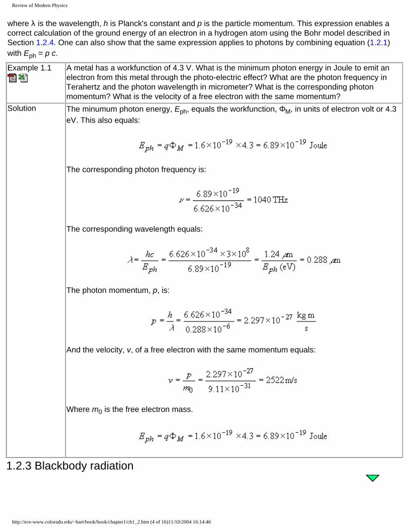
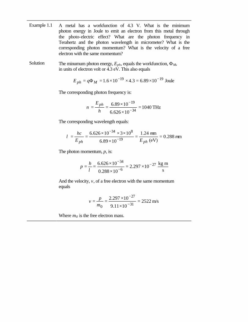
Example 1.1
A metal has a workfunction of 4.3 V. What is the minimum photon energy in Joule to emit an electron from this metal through the photo-electric effect? What are the photon frequency in Terahertz and the photon wavelength in micrometer? What is the corresponding photon momentum? What is the velocity of a free electron with the same momentum?
Solution The minumum photon energy, Eph, equals the workfunction, ΦM, in units of electron volt or 4.3 eV. This also equals:
The corresponding photon frequency is:
The corresponding wavelength equals:
The photon momentum, p, is:
And the velocity, v, of a free electron with the same momentum equals:
Where m0 is the free electron mass.
1.2.3 Blackbody radiation
http://ece-www.colorado.edu/~bart/book/book/chapter1/ch1_2.htm (4 of 16)11/10/2004 16:14:46

Review of Modern Physics
Another experiment which could not be explained without quantum mechanics is the blackbody radiation experiment: By heating an object to high temperatures one finds that it radiates energy in the form of infra-red, visible and ultra-violet light. The appearance is that of a red glow at temperatures around 800° C which becomes brighter at higher temperatures and eventually looks like white light. The spectrum of the radiation is continuous, which led scientists to initially believe that classical electro-magnetic theory should apply. However, all attempts to describe this phenomenon failed until Max Planck developed the blackbody radiation theory based on the assumption that the energy associated with light is quantized and the energy quantum or photon energy equals:
(1.2.3)
Where is the reduced Planck's constant (= h/2π), and ω is the radial frequency (= 2π ν). The spectral density, uω, or the energy density per unit volume and per unit frequency is given by:
(1.2.4)
Where k is Boltzmann's constant and T is the temperature. The spectral density is shown versus energy in Figure 1.2.3.
Figure 1.2.3: Spectral density of a blackbody at 2000, 3000, 4000 and 5000 K versus energy.
The peak value of the blackbody radiation occurs at 2.82 kT and increases with the third power of the temperature. Radiation from the sun closely fits that of a black body at 5800 K.Example 1.2
The spectral density of the sun peaks at a wavelength of 900 nm. If the sun behaves as a black body, what is the temperature of the sun?
http://ece-www.colorado.edu/~bart/book/book/chapter1/ch1_2.htm (5 of 16)11/10/2004 16:14:46

Review of Modern Physics
Solution A wavelength of 900 nm corresponds to a photon energy of:
Since the peak of the spectral density occurs at 2.82 kT, the corresponding temperature equals:
1.2.4 The Bohr model
The spectrum of electromagnetic radiation from an excited hydrogen gas was yet another experiment, which was difficult to explain since it is discreet rather than continuous. The emitted wavelengths were early on associated with a set of discreet energy levels En described by:
(1.2.5)
and the emitted photon energies equal the energy difference released when an electron makes a transition from a higher energy Ei to a lower energy Ej.
(1.2.6)
The maximum photon energy emitted from a hydrogen atom equals 13.6 eV. This energy is also called one Rydberg or one atomic unit. The electron transitions and the resulting photon energies are further illustrated by Figure 1.2.4.
http://ece-www.colorado.edu/~bart/book/book/chapter1/ch1_2.htm (6 of 16)11/10/2004 16:14:46

Review of Modern Physics
Figure 1.2.4 : Energy levels and possible electronic transitions in a hydrogen atom. Shown are the first six energy levels, as well as six possible transitions involving the lowest energy level (n = 1)
However, there was no explanation why the possible energy values were not continuous. No classical theory based on Newtonian mechanics could provide such spectrum. Further more, there was no theory, which could explain these specific values.Niels Bohr provided a part of the puzzle. He assumed that electrons move along a circular trajectory around the proton like the earth around the sun, as shown in Figure 1.2.5.
Figure 1.2.5: Trajectory of an electron in a hydrogen atom as used in the Bohr model.He also assumed that electrons behave within the hydrogen atom as a wave rather than a particle. Therefore, the orbit-like electron trajectories around the proton are limited to those with a length, which equals an integer number of wavelengths so that
(1.2.7)where r is the radius of the circular electron trajectory and n is a positive integer. The Bohr model also assumes that the momentum of the particle is linked to the de Broglie wavelength (equation (1.2.2))
The model further assumes a circular trajectory and that the centrifugal force equals the electrostatic force, or:
(1.2.8)
Solving for the radius of the trajectory one finds the Bohr radius, a0:
(1.2.9)
and the corresponding energy is obtained by adding the kinetic energy and the potential energy of the particle, yielding:
(1.2.10)
Where the potential energy is the electrostatic potential of the proton:
(1.2.11)
Note that all the possible energy values are negative. Electrons with positive energy are not bound to the proton and behave as free electrons.
http://ece-www.colorado.edu/~bart/book/book/chapter1/ch1_2.htm (7 of 16)11/10/2004 16:14:46
Review of Modern Physics
The Bohr model does provide the correct electron energies. However, it leaves many unanswered questions and, more importantly, it does not provide a general method to solve other problems of this type. The wave equation of electrons presented in the next section does provide a way to solve any quantum mechanical problem.
1.2.5 Schrödinger's equation
1.2.5.1. Physical interpretation of the wavefunction1.2.5.2. The infinite quantum well1.2.5.3. The hydrogen atom
A general procedure to solve quantum mechanical problems was proposed by Erwin Schrödinger. Starting from a classical description of the total energy, E, which equals the sum of the kinetic energy, K.E., and potential energy, V, or:
(1.2.12)
He converted this expression into a wave equation by defining a wavefunction, Ψ, and multiplied each term in the equation with that wavefunction:
(1.2.13)
To incorporate the de Broglie wavelength of the particle we now introduce the operator, , which provides the square of the momentum, p, when applied to a plane wave:
(1.2.14)
Where k is the wavenumber, which equals 2π /λ. Without claiming that this is an actual proof we now simply replace the momentum squared, p2, in equation (1.2.13) by this operator yielding the time-independent Schrödinger equation.
(1.2.15)
To illustrate the use of Schrödinger's equation, we present two solutions of Schrödinger's equation, that for an infinite quantum well and that for the hydrogen atom. Prior to that, we discuss the physical interpretation of the wavefunction.
1.2.5.1. Physical interpretation of the wavefunction
The use of a wavefunction to describe a particle, as in the Schrödinger equation, is consistent with the particle-wave duality concept. However, the physical meaning of the wavefunction does not naturally follow. Quantum theory postulates that the wavefunction, Ψ(x), multiplied with its complex conjugate, Ψ*(x), is proportional to the probability density function, P(x), associated with that particle
http://ece-www.colorado.edu/~bart/book/book/chapter1/ch1_2.htm (8 of 16)11/10/2004 16:14:46
Review of Modern Physics
(1.2.16)
This probability density function integrated over a specific volume provides the probability that the particle described by the wavefunction is within that volume. The probability function is frequently normalized to indicate that the probability of finding the particle somewhere equals 100%. This normalization enables to calculate the magnitude of the wavefunction using:
(1.2.17)
This probability density function can then be used to find all properties of the particle by using the quantum operators. To find the expected value of a function f(x,p) for the particle described by the wavefunction, one calculates:
(1.2.18)
Where F(x) is the quantum operator associated with the function of interest. A list of quantum operators corresponding to a selection of common classical variables is provided in Table 1.2.1.
Table 1.2.1: Selected classical variables and the corresponding quantum operator.
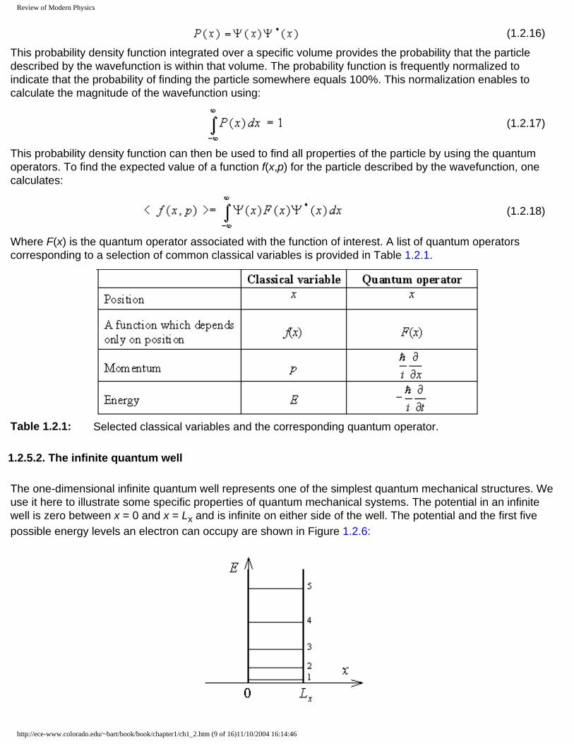
1.2.5.2. The infinite quantum well
The one-dimensional infinite quantum well represents one of the simplest quantum mechanical structures. We use it here to illustrate some specific properties of quantum mechanical systems. The potential in an infinite well is zero between x = 0 and x = Lx and is infinite on either side of the well. The potential and the first five possible energy levels an electron can occupy are shown in Figure 1.2.6:
http://ece-www.colorado.edu/~bart/book/book/chapter1/ch1_2.htm (9 of 16)11/10/2004 16:14:46

Review of Modern Physics
Figure 1.2.6 : Potential energy of an infinite well, with width Lx. Also indicated are the lowest five energy levels in the well.
The energy levels in an infinite quantum well are calculated by solving Schrödinger’s equation 1.2.15 with the potential, V(x), as shown in Figure 1.2.6. As a result one solves the following equation within the well.
(1.2.19)
The general solution to this differential equation is:
(1.2.20)
Where the coefficients A and B must be determined by applying the boundary conditions. Since the potential is infinite on both sides of the well, the probability of finding an electron outside the well and at the well boundary equals zero. Therefore the wave function must be zero on both sides of the infinite quantum well or:
(1.2.21)
These boundary conditions imply that the coefficient B must be zero and the argument of the sine function must equal a multiple of pi at the edge of the quantum well or:
(1.2.22)
Where the subscript n was added to the energy, E, to indicate the energy corresponding to a specific value of, n. The resulting values of the energy, En, are then equal to:
(1.2.23)
The corresponding normalized wave functions, Ψn(x), then equal:
(1.2.24)
where the coefficient A was determined by requiring that the probability of finding the electron in the well equals unity or:
(1.2.25)
The asterisk denotes the complex conjugate.Note that the lowest possible energy is not zero although the potential is zero within the well. Only discreet energy values are obtained as eigenvalues of the Schrödinger equation. The energy difference between adjacent energy levels increases as the energy increases. An electron occupying one of the energy levels can have a positive or negative spin (s = 1/2 or s = -1/2). Both quantum numbers, n and s, are the only two quantum numbers needed to describe this system.
http://ece-www.colorado.edu/~bart/book/book/chapter1/ch1_2.htm (10 of 16)11/10/2004 16:14:46

Review of Modern Physics
The wavefunctions corresponding to each energy level are shown in Figure 1.2.7 (a). Each wavefunction has been shifted by the corresponding energy. The probability density function, calculated as |Ψ|2, provides the probability of finding an electron in a certain location in the well. These probability density functions are shown in Figure 1.2.7 (b) for the first five energy levels. For instance, for n = 2 the electron is least likely to be in the middle of the well and at the edges of the well. The electron is most likely to be one quarter of the well width away from either edge.
Figure 1.2.7 : Energy levels, wavefunctions (left) and probability density functions (right) in an infinite quantum well. The figure is calculated for a 10 nm wide well containing an electron with mass m0. The wavefunctions and the probability density functions are not normalized and shifted by the corresponding electron energy.
Example 1.3
An electron is confined to a 1 micron thin layer of silicon. Assuming that the semiconductor can be adequately described by a one-dimensional quantum well with infinite walls, calculate the lowest possible energy within the material in units of electron volt. If the energy is interpreted as the kinetic energy of the electron, what is the corresponding electron velocity? (The effective mass of electrons in silicon is 0.26 m0, where m0 = 9.11 x 10⁻³¹ kg is the free electron rest mass).
Solution The lowest energy in the quantum well equals:
= 2.32 x 10⁻²⁵ Joules = 1.45 meV
The velocity of an electron with this energy equals:
=1.399 km/s
http://ece-www.colorado.edu/~bart/book/book/chapter1/ch1_2.htm (11 of 16)11/10/2004 16:14:46

Review of Modern Physics
1.2.5.3. The hydrogen atom
The hydrogen atom represents the simplest possible atom since it consists of only one proton and one electron. Nevertheless, the solution to Schrödinger's equation as applied to the potential of the hydrogen atom is rather complex due to the three-dimensional nature of the problem. The potential, V(r) (equation (1.2.11)), is due to the electrostatic force between the positively charged proton and the negatively charged electron.
(1.2.26)
The energy levels in a hydrogen atom can be obtained by solving Schrödinger’s equation in three dimensions.
(1.2.27)
The potential V(x,y,z) is the electrostatic potential, which describes the attractive force between the positively charged proton and the negatively charged electron. Since this potential depends on the distance between the two charged particles one typically assumes that the proton is placed at the origin of the coordinate system and the position of the electron is indicated in polar coordinates by its distance r from the origin, the polar angle θ and the azimuthal angle φ.
Schrödinger’s equation becomes:
(1.2.28)
A more refined analysis includes the fact that the proton moves as the electron circles around it, despite its much larger mass. The stationary point in the hydrogen atom is the center of mass of the two particles. This refinement can be included by replacing the electron mass, m, with the reduced mass, mr, which includes both the electron and proton mass:
(1.2.29)
Schrödinger’s equation is then solved by using spherical coordinates, resulting in:
(1.2.30)
In addition, one assumes that the wavefunction, Ψ(r,θ,φ), can be written as a product of a radial, angular and azimuthal angular wavefunction, R(r), Θ(θ) and Φ(φ). This assumption allows the separation of variables, i.e. the reformulation of the problem into three different differential equations, each containing only a single variable, r, θ or φ:
(1.2.31)
(1.2.32)
http://ece-www.colorado.edu/~bart/book/book/chapter1/ch1_2.htm (12 of 16)11/10/2004 16:14:46

Review of Modern Physics
(1.2.33)
Where the constants A and B are to be determined. The solution to these differential equations is beyond the scope of this text. Readers are referred to the bibliography for an in depth treatment. We will now examine and discuss the solution.
The electron energies in the hydrogen atom as obtained from equation (1.2.31) are:
(1.2.34)
Where n is the principal quantum number.
This potential as well as the first three probability density functions (r2|Ψ|2) of the radially symmetric wavefunctions (l = 0) is shown in Figure 1.2.8.
Figure 1.2.8 : Potential energy, V(x), in a hydrogen atom and first three probability densities with l = 0. The probability densities are shifted by the corresponding electron energy.
Since the hydrogen atom is a three-dimensional problem, three quantum numbers, labeled n, l, and m, are needed to describe all possible solutions to Schrödinger's equation. The spin of the electron is described by the quantum number s. The energy levels only depend on n, the principal quantum number and are given by equation (1.2.10). The electron wavefunctions however are different for every different set of quantum numbers. While a derivation of the actual wavefunctions is beyond the scope of this text, a list of the possible quantum numbers is needed for further discussion and is therefore provided in Table 1.2.1. For each principal quantum number n, all smaller positive integers are possible values for the angular momentum quantum number l. The quantum number m can take on all integers between l and -l, while s can be ½ or -½. This leads to a maximum of 2 unique sets of quantum numbers for all s orbitals (l = 0), 6 for all p orbitals (l = 1), 10 for all d orbitals (l = 2) and 14 for all f orbitals (l = 3).
http://ece-www.colorado.edu/~bart/book/book/chapter1/ch1_2.htm (13 of 16)11/10/2004 16:14:46

Review of Modern Physics
Table 1.2.2: First ten orbitals and corresponding quantum numbers of a hydrogen atom
1.2.6 Pauli exclusion principle
Once the energy levels of an atom are known, one can find the electron configurations of the atom, provided the number of electrons occupying each energy level is known. Electrons are Fermions since they have a half integer spin. They must therefore obey the Pauli exclusion principle. This exclusion principle states that no two Fermions can occupy the same energy level corresponding to a unique set of quantum numbers n, l, m or s. The ground state of an atom is therefore obtained by filling each energy level, starting with the lowest energy, up to the maximum number as allowed by the Pauli exclusion principle.
1.2.7 Electronic configuration of the elements
The electronic configuration of the elements of the periodic table can be constructed using the quantum numbers of the hydrogen atom and the Pauli exclusion principle, starting with the lightest element hydrogen. Hydrogen contains only one proton and one electron. The electron therefore occupies the lowest energy level of the hydrogen atom, characterized by the principal quantum number n = 1. The orbital quantum number l equals zero and is referred to as an s orbital (not to be confused with the quantum number for spin, s). The s orbital can accommodate two electrons with opposite spin, but only one is occupied. This leads to the short-hand notation of 1s1 for the electronic configuration of hydrogen as listed in Table 1.2.2.
Helium is the second element of the periodic table. For this and all other atoms one still uses the same quantum numbers as for the hydrogen atom. This approach is justified since all atom cores can be treated as a single charged particle, which yields a potential very similar to that of a proton. While the electron energies are no longer the same as for the hydrogen atom, the electron wavefunctions are very similar and can be classified in the same way. Since helium contains two electrons it can accommodate two electrons in the 1s orbital, hence the notation 1s2. Since the s orbitals can only accommodate two electrons, this orbital is now completely filled, so that all other atoms will have more than one filled or partially-filled orbital. The two electrons in the helium atom also fill all available orbitals associated with the first principal quantum number, yielding a filled outer shell. Atoms with a filled outer shell are called noble gases as they are known to be chemically inert.
http://ece-www.colorado.edu/~bart/book/book/chapter1/ch1_2.htm (14 of 16)11/10/2004 16:14:46

Review of Modern Physics
Lithium contains three electrons and therefore has a completely filled 1s orbital and one more electron in the next higher 2s orbital. The electronic configuration is therefore 1s22s1 or [He]2s1, where [He] refers to the electronic configuration of helium. Beryllium has four electrons, two in the 1s orbital and two in the 2s orbital. The next six atoms also have a completely filled 1s and 2s orbital as well as the remaining number of electrons in the 2p orbitals. Neon has six electrons in the 2p orbitals, thereby completely filling the outer shell of this noble gas.The next eight elements follow the same pattern leading to argon, the third noble gas. After that the pattern changes as the underlying 3d orbitals of the transition metals (scandium through zinc) are filled before the 4p orbitals, leading eventually to the fourth noble gas, krypton. Exceptions are chromium and zinc, which have one more electron in the 3d orbital and only one electron in the 4s orbital. A similar pattern change occurs for the remaining transition metals, where for the lanthanides and actinides the underlying f orbitals are filled first.
http://ece-www.colorado.edu/~bart/book/book/chapter1/ch1_2.htm (15 of 16)11/10/2004 16:14:46

Review of Modern Physics
Table 1.2.3: Electronic configuration of the first thirty-six elements of the periodic table.
http://ece-www.colorado.edu/~bart/book/book/chapter1/ch1_2.htm (16 of 16)11/10/2004 16:14:46
Electromagnetic Theory
Title Page Table of Contents Help Copyright B. Van Zeghbroeck, 2004
Chapter 1: Review of Modern Physics
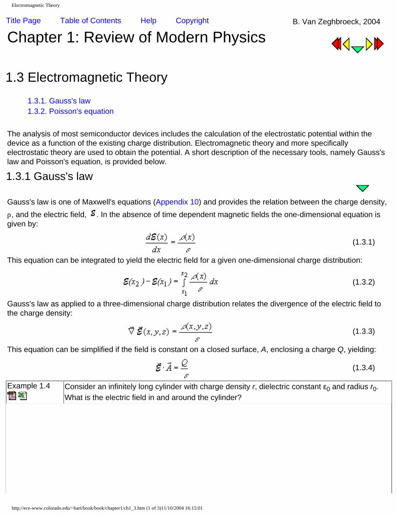
1.3 Electromagnetic Theory1.3.1. Gauss's law1.3.2. Poisson's equation
The analysis of most semiconductor devices includes the calculation of the electrostatic potential within the device as a function of the existing charge distribution. Electromagnetic theory and more specifically electrostatic theory are used to obtain the potential. A short description of the necessary tools, namely Gauss's law and Poisson's equation, is provided below.
1.3.1 Gauss's law
Gauss's law is one of Maxwell's equations (Appendix 10) and provides the relation between the charge density, ρ, and the electric field, . In the absence of time dependent magnetic fields the one-dimensional equation is given by:
(1.3.1)
This equation can be integrated to yield the electric field for a given one-dimensional charge distribution:
(1.3.2)
Gauss's law as applied to a three-dimensional charge distribution relates the divergence of the electric field to the charge density:
(1.3.3)
This equation can be simplified if the field is constant on a closed surface, A, enclosing a charge Q, yielding:
(1.3.4)
Example 1.4
Consider an infinitely long cylinder with charge density r, dielectric constant ε0 and radius r0. What is the electric field in and around the cylinder?
http://ece-www.colorado.edu/~bart/book/book/chapter1/ch1_3.htm (1 of 3)11/10/2004 16:15:01

Electromagnetic Theory
Solution Because of the cylinder symmetry one expects the electric field to be only dependent on the radius, r. Applying Gauss's law one finds:
and
where a cylinder with length L was chosen to define the surface A, and edge effects were ignored. The electric field then equals:
The electric field increases within the cylinder with increasing radius. The electric field decreases outside the cylinder with increasing radius.
1.3.2 Poisson's equation
Gauss's law is one of Maxwell's equations and provides the relation between the charge density, ρ, and the electric field, . In the absence of time dependent magnetic fields the one-dimensional equation is given by:
(1.3.5)
The electric field vector therefore originates at a point of higher potential and points towards a point of lower potential.The potential can be obtained by integrating the electric field as described by:
(1.3.6)
At times, it is convenient to link the charge density to the potential by combining equation (1.3.5) with Gauss's law in the form of equation (1.3.1), yielding:
(1.3.7)
which is referred to as Poisson's equation.For a three-dimensional field distribution, the gradient of the potential as described by:
(1.3.8)
http://ece-www.colorado.edu/~bart/book/book/chapter1/ch1_3.htm (2 of 3)11/10/2004 16:15:01

Electromagnetic Theory
can be combined with Gauss's law as formulated with equation (1.3.3), yielding a more general form of Poisson's equation:
(1.3.9)
http://ece-www.colorado.edu/~bart/book/book/chapter1/ch1_3.htm (3 of 3)11/10/2004 16:15:01

Statistical Thermodynamics
Title Page Table of Contents Help Copyright B. Van Zeghbroeck, 2004
Chapter 1: Review of Modern Physics
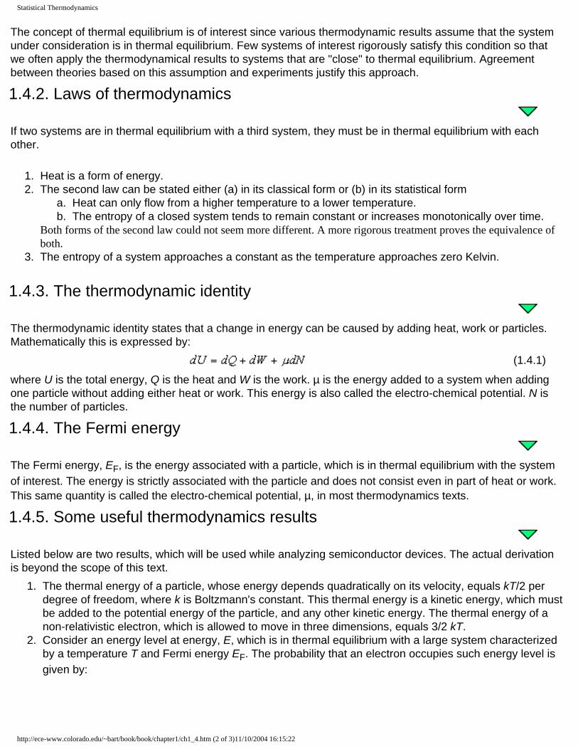
1.4. Statistical Thermodynamics1.4.1. Thermal equilibrium1.4.2. Laws of thermodynamics1.4.3. The thermodynamic identity1.4.4. The Fermi energy1.4.5. Some useful thermodynamics results
Thermodynamics describes the behavior of systems containing a large number of particles. These systems are characterized by their temperature, volume, number and the type of particles. The state of the system is then further described by its total energy and a variety of other parameters including the entropy. Such a characterization of a system is much simpler than trying to keep track of each particle individually, hence its usefulness. In addition, such a characterization is general in nature so that it can be applied to mechanical, electrical and chemical systems.The term thermodynamics is somewhat misleading as one deals primarily with systems in thermal equilibrium. These systems have constant temperature, volume and number of particles and their macroscopic parameters do not change over time, so that the dynamics are limited to the microscopic dynamics of the particles within the system. Statistical thermodynamics is based on the fundamental assumption that all possible configurations of a given system, which satisfy the given boundary conditions such as temperature, volume and number of particles, are equally likely to occur. The overall system will therefore be in the statistically most probable configuration. The entropy of a system is defined as the logarithm of the number of possible configurations. While such definition does not immediately provide insight into the meaning of entropy, it does provide a straightforward analysis since the number of configurations can be calculated for any given system. Classical thermodynamics provides the same concepts. However, they are obtained through experimental observation. The classical analysis is therefore more tangible compared to the abstract mathematical treatment of the statistical approach. The study of semiconductor devices requires some specific results, which naturally emerge from statistical thermodynamics. In this section, we review basic thermodynamic principles as well as some specific results. These include the thermal equilibrium concept, the thermodynamic identity, the basic laws of thermodynamics, the thermal energy per particle and the Fermi function.
1.4.1. Thermal equilibrium
A system is in thermal equilibrium if detailed balance is obtained: i.e. every process in the system is exactly balanced by its inverse process so that there is no net effect on the system. This definition implies that in thermal equilibrium no energy (heat, work or particle energy) is exchanged between the parts within the system or between the system and the environment. Thermal equilibrium is obtained by isolating a system from its environment, removing any internal sources of energy, and waiting for a long enough time until the system does not change any more.
http://ece-www.colorado.edu/~bart/book/book/chapter1/ch1_4.htm (1 of 3)11/10/2004 16:15:22
Statistical Thermodynamics
The concept of thermal equilibrium is of interest since various thermodynamic results assume that the system under consideration is in thermal equilibrium. Few systems of interest rigorously satisfy this condition so that we often apply the thermodynamical results to systems that are "close" to thermal equilibrium. Agreement between theories based on this assumption and experiments justify this approach.
1.4.2. Laws of thermodynamics
If two systems are in thermal equilibrium with a third system, they must be in thermal equilibrium with each other.
1. Heat is a form of energy.2. The second law can be stated either (a) in its classical form or (b) in its statistical form
a. Heat can only flow from a higher temperature to a lower temperature.b. The entropy of a closed system tends to remain constant or increases monotonically over time.
Both forms of the second law could not seem more different. A more rigorous treatment proves the equivalence of both.
3. The entropy of a system approaches a constant as the temperature approaches zero Kelvin.
1.4.3. The thermodynamic identity
The thermodynamic identity states that a change in energy can be caused by adding heat, work or particles. Mathematically this is expressed by:
(1.4.1)
where U is the total energy, Q is the heat and W is the work. µ is the energy added to a system when adding one particle without adding either heat or work. This energy is also called the electro-chemical potential. N is the number of particles.
1.4.4. The Fermi energy
The Fermi energy, EF, is the energy associated with a particle, which is in thermal equilibrium with the system of interest. The energy is strictly associated with the particle and does not consist even in part of heat or work. This same quantity is called the electro-chemical potential, µ, in most thermodynamics texts.
1.4.5. Some useful thermodynamics results
Listed below are two results, which will be used while analyzing semiconductor devices. The actual derivation is beyond the scope of this text.
1. The thermal energy of a particle, whose energy depends quadratically on its velocity, equals kT/2 per degree of freedom, where k is Boltzmann's constant. This thermal energy is a kinetic energy, which must be added to the potential energy of the particle, and any other kinetic energy. The thermal energy of a non-relativistic electron, which is allowed to move in three dimensions, equals 3/2 kT.
2. Consider an energy level at energy, E, which is in thermal equilibrium with a large system characterized by a temperature T and Fermi energy EF. The probability that an electron occupies such energy level is given by:
http://ece-www.colorado.edu/~bart/book/book/chapter1/ch1_4.htm (2 of 3)11/10/2004 16:15:22
Statistical Thermodynamics
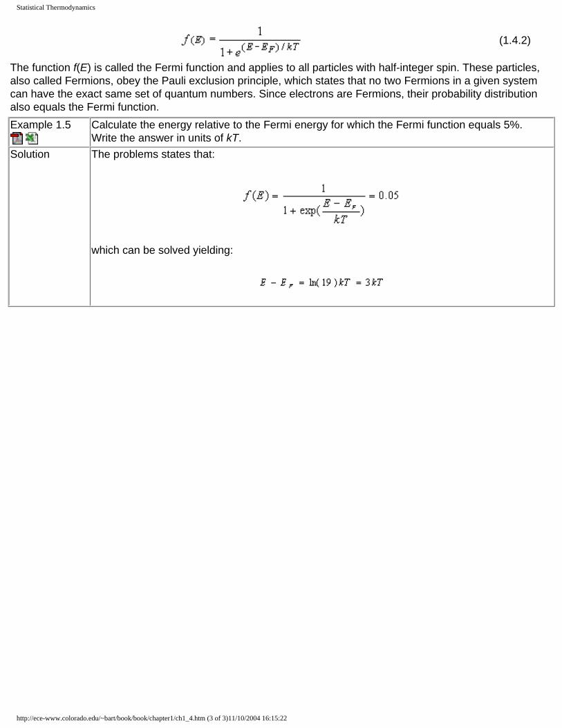
(1.4.2)
The function f(E) is called the Fermi function and applies to all particles with half-integer spin. These particles, also called Fermions, obey the Pauli exclusion principle, which states that no two Fermions in a given system can have the exact same set of quantum numbers. Since electrons are Fermions, their probability distribution also equals the Fermi function.Example 1.5
Calculate the energy relative to the Fermi energy for which the Fermi function equals 5%. Write the answer in units of kT.
Solution The problems states that:
which can be solved yielding:
http://ece-www.colorado.edu/~bart/book/book/chapter1/ch1_4.htm (3 of 3)11/10/2004 16:15:22

Chapter 1 Examples
Title Page Table of Contents Help Copyright B. Van Zeghbroeck, 2004
Chapter 1: Review of Modern Physics
Examples
Example 1.1 A metal has a workfunction of 4.3 V. What is the minimum photon energy in Joule to emit an electron from this metal through the photo-electric effect? What are the photon frequency in Terahertz and the photon wavelength in micrometer? What is the corresponding photon momentum? What is the velocity of a free electron with the same momentum?
Example 1.2 The spectral density of the sun peaks at a wavelength of 900 nm. If the sun behaves as a black body, what is the temperature of the sun?
Example 1.3 An electron is confined to a 1 micron thin layer of silicon. Assuming that the semiconductor can be adequately described by a one-dimensional quantum well with infinite walls, calculate the lowest possible energy within the material in units of electron volt. If the energy is interpreted as the kinetic energy of the electron, what is the corresponding electron velocity? (The effective mass of electrons in silicon is 0.26 m0, where m0 = 9.11 x 10⁻³¹ kg is the free electron rest mass).
Example 1.4 Consider an infinitely long cylinder with charge density r, dielectric constant ε0 and radius r0. What is the electric field in and around the cylinder?
Example 1.5 Calculate the energy relative to the Fermi energy for which the Fermi function equals 5%. Write the answer in units of kT.
http://ece-www.colorado.edu/~bart/book/book/chapter1/ch1_ex.htm11/10/2004 16:15:39
Example 1.1 A metal has a workfunction of 4.3 V. What is the minimum photon energy in Joule to emit an electron from this metal through the photo-electric effect? What are the photon frequency in Terahertz and the photon wavelength in micrometer? What is the corresponding photon momentum? What is the velocity of a free electron with the same momentum?
Solution The minumum photon energy, Eph, equals the workfunction, ΦM, in units of electron volt or 4.3 eV. This also equals
Joule 1089.63.4106.1 1919 −− ×=××=Φ= Mph qE
The corresponding photon frequency is:
THz 104010626.6
1089.634
19=
×
×==
−
−
h
E phν
The corresponding wavelength equals:
m 288.0(eV)
m 24.1
1089.6
10310626.619
834µ
µλ ==
×
×××== −
−
phph EEhc
The photon momentum, p, is:
sm kg
10297.210288.0
10626.6 276
34−
−
−×=
×
×==
λh
p
And the velocity, v, of a free electron with the same momentum equals
m/s 25221011.9
10297.231
27
0=
×
×==
−
−
mp
v
Where m0 is the free electron mass.

Example 1.2 The spectral density of the sun peaks at a wavelength of 900 nm. If the sun behaves as a black body, what is the temperature of the sun?
Solution A wavelength of 900 nm corresponds to a photon energy of:
Joule 1021.210900
10310626.6 199
834−
−
−
×=×
×××==
λhc
E ph
Since the peak of the spectral density occurs at 2.82 kT, the corresponding temperature equals:
Kelvin 56721038.182.2
1021.282.2 23
19
=××
×==
−
−
k
ET ph

08/30/00 © B. Van Zeghbroeck, 1998
Example 1.3 An electron is confined to a 1 micron thin layer of silicon. Assuming that the semiconductor can be adequately described by a one-dimensional quantum well with infinite walls, calculate the lowest possible energy within the material in units of electron volt. If the energy is interpreted as the kinetic energy of the electron, what is the corresponding electron velocity? (The effective mass of electrons in silicon is 0.26 m0, where m0 = 9.11 x 10⁻³¹ kg is the free electron rest mass).
Solution The lowest energy in the quantum well equals:
2631
2342
*
2
1 )1021
(1011.926.02)10626.6(
)21
(2 −−
−
×××××
==xLm
hE
= 2.32 x 10⁻²⁵ Joules = 1.45 µeV
The velocity of an electron with this energy equals:
31
25
*1
1011.926.01032.222
−
−
××××
==mE
v =1.399 km/s

09/04/02 © B. Van Zeghbroeck, 1998
Example 1.4 Consider an infinitely long cylinder with charge density ρ, dielectric constant ε0 and radius r0. What is the electric field in and around the cylinder?
Solution Because of the cylinder symmetry one expects the electric field to be only dependent on the radius, r. Applying Gauss's law one finds:
0
2
0
2ε
ρπε
πLrQ
rLA ===⋅ EE for r < r0
and
0
20
0
2ε
ρπε
πLrQ
rLA ===⋅ EE for r > r0
where a cylinder with length L was chosen to define the surface A, and edge effects were ignored. The electric field then equals:
02)(
ερ r
r =E for r < r0 and r
rr
0
20
2)(
ερ
=E for r > r0
The electric field therefore increases within the cylinder with increasing radius as shown in the figure below. The electric field decreases outside the cylinder with increasing radius.
r0
ε 0
rρ
L
r0
ε 0
rρ
L
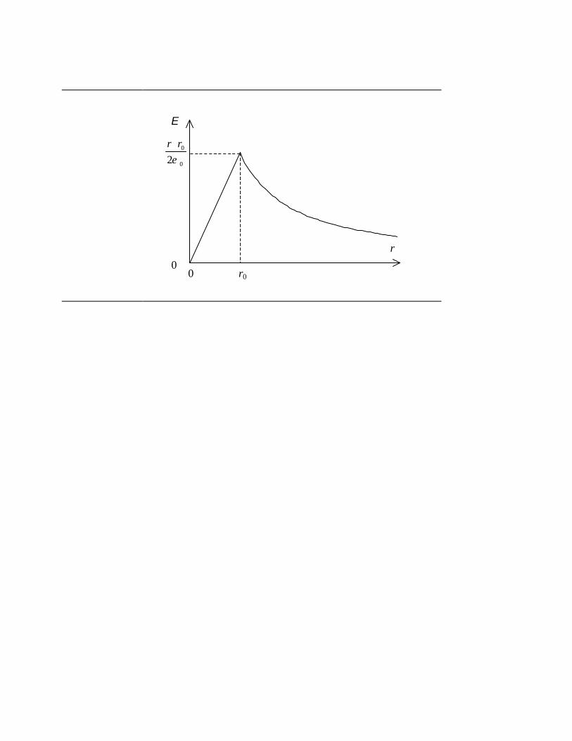
r
0 0
r0
E
0
0
2ερ r

08/30/00 © B. Van Zeghbroeck, 1998
Example 1.5 Calculate the energy relative to the Fermi energy for which the Fermi function equals 5%. Write the answer in units of kT.
Solution The problems states that:
05.0)exp(1
1)( =
−+
=
kTEE
EfF
which can be solved yielding:
kTkTEE F 3)19ln( ==−
http://ece-www.colorado.edu/~bart/book/book/chapter1/ch1_p.htm
Title Page Table of Contents Help Copyright B. Van Zeghbroeck, 2004
Chapter 1: Review of Modern Physics
Problems
1. Calculate the wavelength of a photon with a photon energy of 2 eV. Also, calculate the wavelength of an electron with a kinetic energy of 2 eV.
2. Consider a beam of light with a power of 1 Watt and a wavelength of 800 nm. Calculate a) the photon energy of the photons in the beam, b) the frequency of the light wave and c) the number of photons provided by the beam in one second.
3. Show that the spectral density, uω (equation 1.2.4) peaks at Eph = 2.82 kT. Note that a numeric iteration
is required.
4. Calculate the peak wavelength of blackbody radiation emitted from a human body at a temperature of 37°C.
5. Derive equations (1.2.9) and (1.2.10).
6. What is the width of an infinite quantum well if the second lowest energy of a free electron confined to the well equals 100 meV.
7. Calculate the lowest three possible energies of an electron in a hydrogen atom in units of electron volt.
8. Derive the electric field of a proton with charge q as a function of the distance from the proton using Gauss's law. Integrated the electric field to find the potential φ(r):
Treat the proton as a point charge and assume the potential to be zero far away from the proton.
9. Prove that the probability of occupying an energy level below the Fermi energy equals the probability that an energy level above the Fermi energy and equally far away from the Fermi energy is not occupied.
10. The ratio of the wavelengths emitted by two electrons in an infinite quantum well while making the transition from a higher energy level to the lowest possible energy equals two.
a. a) What are the lowest possible quantum numbers (n) of the two higher energy levels, which are consistent with the statement above?
http://ece-www.colorado.edu/~bart/book/book/chapter1/ch1_p.htm (1 of 2)11/10/2004 16:16:49

http://ece-www.colorado.edu/~bart/book/book/chapter1/ch1_p.htm
b. What are the energies in electron volt of all three energy levels involved in the transitions? (Lx = 10 nm, m*/m0 = 0.067 and εs/ε0 = 13, m0 = 9.11 x 10⁻³¹ kg, ε0 = 8.854 x 10⁻¹² F/m)
11. Consider a hollow thin conducting sphere of radius R = 10 cm, uniformly distributed with a surface charge density of σ = 10-9 coulombs/cm2. a) Find the field at a radius r > 10 cm. Explain the vector orientation of the field and the magnitude. b) Find the field at a radius r < 10 cm inside the sphere. Explain the vector orientation of the field and the magnitude. c) Now consider two concentric conducting spherical shells, each coated with a uniformly distributed surface charge density of σ with R1 = R and R2
= R/2. Find the field at all r.
12. Find the lowest possible energy in a 2 nm quantum well with infinitely high barriers on each side of the well and with a delta function potential positioned in the middle of the quantum well. The integral of the delta function potential equals 10-10 eV-m. Assume that the electron mass equals the free electron mass (m0 = 9.1 x 10⁻³¹ kg).
13. Consider the potential energy, V(x), as shown in the figure below, where E is the particle energy:
a. Find a general solution to the wave equation in region I (0 < x < L) and II (L < x < 2L). Assume that the particle energy is always larger than the potential V0.
b. Require that the wavefunction is zero at x = 0 and x = 2L. c. Require that the wavefunction and it's derivative is continuous at x = L. d. Derive a transcendental equation from which the possible energies can be obtained. e. Calculate the lowest possible energy for V0 = 0.1 eV, L = 1 nm and m = m0.
http://ece-www.colorado.edu/~bart/book/book/chapter1/ch1_p.htm (2 of 2)11/10/2004 16:16:49

Problems 1. Calculate the wavelength of a photon with a photon energy of 2 eV. Also, calculate the
wavelength of an electron with a kinetic energy of 2 eV.
2. Consider a beam of light with a power of 1 Watt and a wavelength of 800 nm. Calculate a) the photon energy of the photons in the beam, b) the frequency of the light wave and c) the number of photons provided by the beam in one second.
3. Show that the spectral density, uω (equation 1.2.4) peaks at Eph = 2.82 kT. Note that a numeric iteration is required.
4. Calculate the peak wavelength of blackbody radiation emitted from a human body at a temperature of 37°C.
5. Derive equations (1.2.9) and (1.2.10).
6. What is the width of an infinite quantum well if the second lowest energy of a free electron confined to the well equals 100 meV?
7. Calculate the three lowest possible energies of an electron in a hydrogen atom in units of electron volt. Identify all possible electron energies between the lowest energy and -2 eV.
8. Derive the electric field of a proton with charge q as a function of the distance from the proton using Gauss's law. Integrated the electric field to find the potential φ(r):
rq
rsεπ
φ4
)( =
Treat the proton as a point charge and assume the potential to be zero far away from the proton.
9. Prove that the probability of occupying an energy level below the Fermi energy equals the probability that an energy level above the Fermi energy and equally far away from the Fermi energy is not occupied.
10. The ratio of the wavelengths emitted by two electrons in an infinite quantum well while making the transition from a higher energy level to the lowest possible energy equals two.
a) What are the lowest possible quantum numbers (n) of the two higher energy levels, which are consistent with the statement above?
b) What are the energies in electron volt of all three energy levels involved in the transitions? (Lx = 10 nm, m*/m0 = 0.067 and εs/ε0 = 13, m0 = 9.11 x 10⁻³¹ kg, ε0 = 8.854 x 10⁻¹² F/m)
11. Consider a hollow thin conducting sphere of radius R = 10 cm, uniformly distributed with a surface charge density of σ = 10-9 coulombs/cm2.
a) Find the field at a radius r > 10 cm. Explain the vector orientation of the field and the magnitude.

2 Chapter 1
b) Find the field at a radius r < 10 cm inside the sphere. Explain the vector orientation of the field and the magnitude.
c) Now consider two concentric conducting spherical shells, each coated with a uniformly distributed surface charge density of σ with R1 = R and R2 = R/2. Find the field at all r.
12. Find the lowest possible energy in a 2 nm quantum well with infinitely high barriers on each side of the well and with a delta function potential positioned in the middle of the quantum well. The integral of the delta function potential equals 10-10 eV-m. Assume that the electron mass equals the free electron mass (m0 = 9.1 x 10⁻³¹ kg).
13. Consider the potential energy, V(x), as shown in the figure below, where E is the particle energy:
0
E
2L
x0
L
V
V(x)
a) Find a general solution to the wave equation in region I (0 < x < L) and II (L < x < 2L). Assume that the particle energy is always larger than the potential V0.
b) Require that the wavefunction is zero at x = 0 and x = 2L.
c) Require that the wavefunction and it's derivative is continuous at x = L.
d) Derive a transcendental equation from which the possible energies can be obtained.
e) Calculate the lowest possible energy for V0 = 0.1 eV, L = 1 nm and m = m0.

Problem 1.1 Calculate the wavelength of a photon with a photon energy of 2
eV. Also, calculate the wavelength of an electron with a kinetic energy of 2 eV.
Solution The wavelength of a 2 eV photon equals:
eV2C10602.1
m/s103Js10626.619
834
××
×××== −
−
phEhc
λ = 0.62 µm
where the photon energy (2 eV) was first converted to Joules by multiplying with the electronic charge. The wavelength of an electron with a kinetic energy of 2 eV is obtained by calculating the deBroglie wavelength:
m/s kg1062.7
Js10626.625
34
−
−
×
×==
ph
λ = 0.87 nm
Where the momentum of the particle was calculated from the kinetic energy:
== mEp 2
m/s kg1064.7eV 2C106.1kg1011.92 251931 −−− ×=×××××

Problem 1.2 Consider a beam of light with a power of 1 Watt and a wavelength
of 800 nm. Calculate a) the photon energy of the photons in the beam, b) the frequency of the light wave and c) the number of photons provided by the beam in one second.
Solution The photon energy is calculated from the wavelength as:
m 10800
m/s 103Js10626.69
834
−
−
×
×××==
λhc
E ph = 2.48 x 10⁻¹⁹ J
or in electron Volt:
C 10602.1
J 1048.219
19
−
−
×
×=phE = 1.55 eV
The frequency then equals:
Js 10626.6
J1048.234
19
−
−
×
×==
h
E phν = 375 THz
And the number of photons equals the ratio of the optical power and the energy per photon:
J 1048.2
Watt1 Watt1 photons #
19−×==
phE= 4 x 10¹⁸

Problem 1.3 Show that the spectral density, uω (equation 1.2.4) peaks at Eph =
2.82 kT. Note that a numeric iteration is required. Solution
The spectral density, uω, can be rewritten as a function of kT
xωh
=
1)exp(
3
322
33
−=
xx
c
Tku
πω
h
The maximum of this function is obtained if its derivative is zero or:
0)1)(exp(
)exp(-
1)exp(3
2
32=
−−=
x
xxxx
dxduω
Therefore x must satisfy: xx =−− )exp(33
This transcendental equation can be solved starting with an arbitrary positive value of x. A repeated calculation of the left hand side using this value and the resulting new value for x quickly converges to xmax = 2.82144. The maximum spectral density therefore occurs at:
kT 82144.2maxmax, == kTxE ph
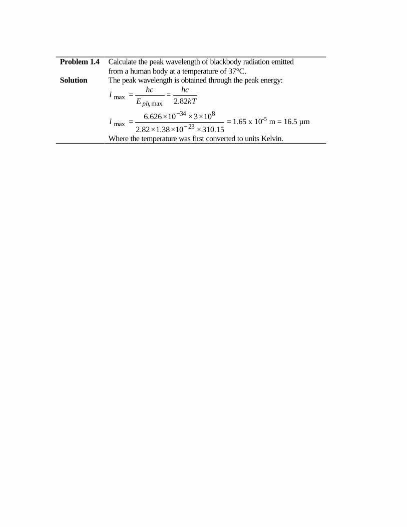
Problem 1.4 Calculate the peak wavelength of blackbody radiation emitted
from a human body at a temperature of 37°C. Solution The peak wavelength is obtained through the peak energy:
kThc
Ehc
ph 82.2max,max ==λ
=×××
×××=
−
−
15.3101038.182.2
10310626.623
834
maxλ 1.65 x 10⁻⁵ m = 16.5 µm
Where the temperature was first converted to units Kelvin.

Problem 1.5 Derive equations (1.2.9) and (1.2.10). Calculate the total energy as
the sum of the kinetic and potential energy. Solution The derivation starts by setting the centrifugal force equal to the
electrostatic force:
20
2
0
22
04 r
qrm
pr
vm
επ==
where the velocity, v, is expressed as a function of the momentum, p. The momentum in turn is calculated as a function of the deBroglie wavelength and the wavelength must be an integer fraction of the length of the circular orbit
20
2
22
22
2
22
44 r
q
rmr
nh
mr
hmrp
εππλ===
The corresponding radius equals the Bohr radius, a0:
20
220
0qm
nha
π
ε=
The corresponding energies are obtained by adding the kinetic and potential energy:
... 2, 1, with , 842 222
0
40
00
2
0
2=−=−= n
nh
qma
qmp
Enεεπ
Note that the potential energy equals the potential of a proton multiplied with the electron charge, -q.

Problem 1.6 What is the width of an infinite quantum well if the second lowest
energy of a free electron confined to the well equals 100 meV? Solution The second lowest energy is calculated from
)2
2(
22
*
2
2xLm
hE = = 1.6 x 10⁻²⁰ J
One can therefore solve for the width, Lx, of the well, yielding:
106.11011.92
10626.6
2 2031
34
2* −−
−
××××
×==
Em
hLx = 3.88 nm

Problem 1.7 Calculate the lowest three possible energies of an electron in a
hydrogen atom in units of electron volt. Identify all possible electron energies between the lowest energy and -2 eV.
Solution The three lowest electron energies in a hydrogen atom can be calculated from:
2eV 6.13
nEn −= , with n = 1, 2, and 3
resulting in: E1 = –13.6 eV, E2 = -3.4 eV and E3 = -1.51 eV
The second lowest energy, E2, is the only one between the lowest energy, E1, and –2 eV.

Problem 1.8 Derive the electric field of a proton with charge q as a function of
the distance from the proton using Gauss's law. Integrate the electric field to find the potential φ(r):
rq
r04
)(επ
φ =
Treat the proton as a point charge and assume the potential to be zero far away from the proton.
Solution Using a sphere with radius, r, around the charged proton as a surface where the electric field, E, is constant, one can apply Gauss’s law:
0
24)(ε
πq
rr =E
so that
024
)(επ r
qr =E
The potential is obtained by integrating this electric field from to Resulting in:
rq
drr
qr
r
020 44
)()(επεπ
φφ =−=∞− ∫∞
where the potential at infinity was set to zero.

Problem 1.9 Prove that the probability of occupying an energy level below the
Fermi energy equals the probability that an energy level above the Fermi energy and equally far away from the Fermi energy is not occupied.
Solution The probability that an energy level with energy ∆E below the Fermi energy EF is occupied can be rewritten as:
1exp
exp
exp1
1)(
+∆
∆
=−∆−
+=∆−
kTEkT
E
kTEEE
EEfFF
F
)(1exp1
11
1exp
11 EEf
kTEEE
kTE F
FF∆+−=
−∆++
−=+
∆−=
so that it also equals the probability that an energy level with energy ∆E above the Fermi energy, EF, is not occupied.

Problem 1.10 The ratio of the wavelengths emitted by two electrons in an
infinite quantum well while making the transition from a higher energy level to the lowest possible energy equals two. a) What are the lowest possible quantum numbers (n) of the
two higher energy levels, which are consistent with the statement above?
b) What are the energies in electron volt of all three energy levels involved in the transitions? (Lx = 10 nm, m*/m0 = 0.067 and εs/ε0 = 13, m0 = 9.11 x 10⁻³¹ kg, ε0 = 8.854 x 10⁻¹² F/m)
Solution a) If the ratio of the wavelengths equals two, the ratio of the energy different between each energy level and the lowest energy level (E1) must equal two as well, so that:
)(2 11 EEEE yx −=− so that
)1(21 22 −=− yx from which )1(21 2 −+= yx and x as well as y must be positive integers larger than 1. for x = 2, 3, 4, 5, 6 and 7 one finds y = 2.65, 4.12, 5.57, 7.00, 8.43 and 9.85. The lowest integers that satisfy the requirement are 5 and 7. The next higher set of integers is 29 and 41.
b) The corresponding energies are:
2*
2
)2
(2 x
n Ln
mh
E = for n = 1, 5 and 7
resulting in E1 = 0.11 eV, E5 = 0.56 and E7 = 0.79 eV The dielectric constant is not used for this problem
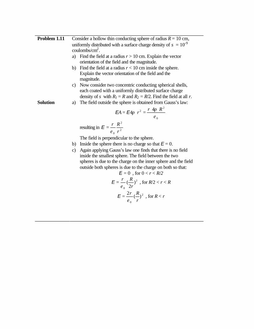
Problem 1.11 Consider a hollow thin conducting sphere of radius R = 10 cm,
uniformly distributed with a surface charge density of σ = 10-9 coulombs/cm2. a) Find the field at a radius r > 10 cm. Explain the vector
orientation of the field and the magnitude. b) Find the field at a radius r < 10 cm inside the sphere.
Explain the vector orientation of the field and the magnitude.
c) Now consider two concentric conducting spherical shells, each coated with a uniformly distributed surface charge density of σ with R1 = R and R2 = R/2. Find the field at all r.
Solution a) The field outside the sphere is obtained from Gauss’s law:
0
22 4
4επρ
πR
rA == EE
resulting in 2
2
0 rR
ερ
=E
The field is perpendicular to the sphere. b) Inside the sphere there is no charge so that E = 0. c) Again applying Gauss’s law one finds that there is no field
inside the smallest sphere. The field between the two spheres is due to the charge on the inner sphere and the field outside both spheres is due to the charge on both so that:
0=E , for 0 < r < R/2 2
0
)2
(r
Rερ
=E , for R/2 < r < R
2
0
)(2
rR
ερ
=E , for R < r

Problem 1.12 Find the lowest possible energy in a 2 nm quantum well with
infinitely high barriers on each side of the well and with a delta function potential positioned in the middle of the quantum well. The integral of the delta function potential equals 10-10 eV-m. Assume that the electron mass equals the free electron mass (m0 = 9.1 x 10⁻³¹ kg).
Solution The general solutions to the wave equation in the quantum well on each side of the delta function are:
)cos()sin()( kxCkxAxI +=Ψ
with hmE
k2
= and
))(cos())(sin()( xLkDxLkBxII −+−=Ψ To satisfy the boundary conditions at x = 0 and x = L C and D need to be zero. At x = L/2 the wave function must be continuous:
)2/sin()2/sin( kLBkLA = so that A = B. Integration of Schrodinger’s equation provides the relation between the derivative of the wavefunction on either side of the delta function:
0)2/(][2 2/2/
2
==Ψ+Ψ
−Ψ
−==
LxAdx
ddx
dm lx
I
lx
IIδ
h
where Aδ is the area of the delta function. Since the wavefunction is continuous at x = L/2 one can use the wavefunction on either side. The resulting equation is then:
)2/sin(2
)2/cos(22
kLAAm
kLkA δh−=
or )2/tan(2
kLAm
k δh−=
The solution is k = 2.13 x 10⁻⁹ m-1. The corresponding energy is E = 0.172 eV

0.000.200.400.600.801.001.20
-2 -1 0 1 2
Distance (nm)
Ele
ctro
n E
nerg
y (e
V)

Problem 1.13 Consider the potential energy, V(x), as shown in the figure
below, where E is the particle energy:
0
E
2L
x0
L
V
V(x)
a) Find a general solution to the wave equation in region I (0 < x < L) and II (L < x < 2L). Assume that the particle energy, E, is always larger than the potential V0.
b) Require that the wavefunction is zero at x = 0 and x = 2L. c) Require that the wavefunction and it's derivative is
continuous at x = L. d) Derive a transcendental equation from which the possible
energies can be obtained. e) Calculate the lowest possible energy for V0 = 0.1 eV, L = 1
nm and m = m0. Solution a) The general solutions to the wave equation are:
)cos()sin()( 11 xkCxkAxI +=Ψ with hmE
k2
1 =
))2(cos())2(sin()( 22 xLkDxLkBxII −+−=Ψ with
h
)(2 02
VEmk
−=
b) To satisfy the boundary conditions C and D need to be zero. c) At x = L the wave function and its derivative need to be
continuous, or: )sin()sin( 21 LkBLkA =
)cos()cos( 2211 LkBkLkAk −= d) Taking the ratio one can eliminate A and B:
))(2
cot()()2
cot( 00 L
VEmVEL
mEE
hh
−−−=
e) Energy equals 138 meV

00.05
0.10.15
0.2
0.250.3
0.0 0.5 1.0 1.5 2.0 2.5
Position (nm)
Ener
gy (e
V)

http://ece-www.colorado.edu/~bart/book/book/chapter1/ch1_r.htm
Title Page Table of Contents Help Copyright B. Van Zeghbroeck, 2004
Chapter 1: Review of Modern Physics
Review Questions
1. List three experiments, which can only be explained using quantum mechanics.
2. What is a Rydberg?
3. Name the two primary assumptions of the Bohr model.
4. How do we know that the energy levels in a hydrogen atom are quantized?
5. What two parameters are linked by Gauss's law?
6. What two parameters are linked by Poisson's equation?
7. What is the definition of thermal equilibrium?
8. List the three laws of thermodynamics.
9. Explain in words the meaning of the thermodynamic identity.
10. What is the Fermi function?
http://ece-www.colorado.edu/~bart/book/book/chapter1/ch1_r.htm11/10/2004 16:20:26

Review Questions 1. List three experiments, which can only be explained using quantum mechanics.
2. What is a Rydberg?
3. Name the two primary assumptions of the Bohr model.
4. How do we know that the energy levels in a hydrogen atom are quantized?
5. What two parameters are linked by Gauss's law?
6. What two parameters are linked by Poisson's equation?
7. What is the definition of thermal equilibrium?
8. List the three laws of thermodynamics.
9. Explain in words the meaning of the thermodynamic identity.
10. What is the Fermi function?

Chapter 1 Bibliography
Title Page Table of Contents Help Copyright B. Van Zeghbroeck, 2004
Chapter 1: Review of Modern Physics
Bibliography
1. Quantum Mechanics, H. Kroemer, Prentice Hall, 1994.
2. Electrons in Solids, Third edition, R.H. Bube, Academic Press, 1992.
3. Solid State Electronic Devices, Fifth edition, B. G. Streetman, Prentice Hall, 2000.
4. Quantum Mechanics, Second edition, E. Merzbacher, Wiley, 1970.
5. Quantum Physics of Electronics, S.N. Levine, The Macmillan company, 1965.
6. Thermal Physics, Second edition, C. Kittel and H. Kroemer, Freeman, 1980.
http://ece-www.colorado.edu/~bart/book/book/chapter1/ch1_b.htm11/10/2004 16:20:53
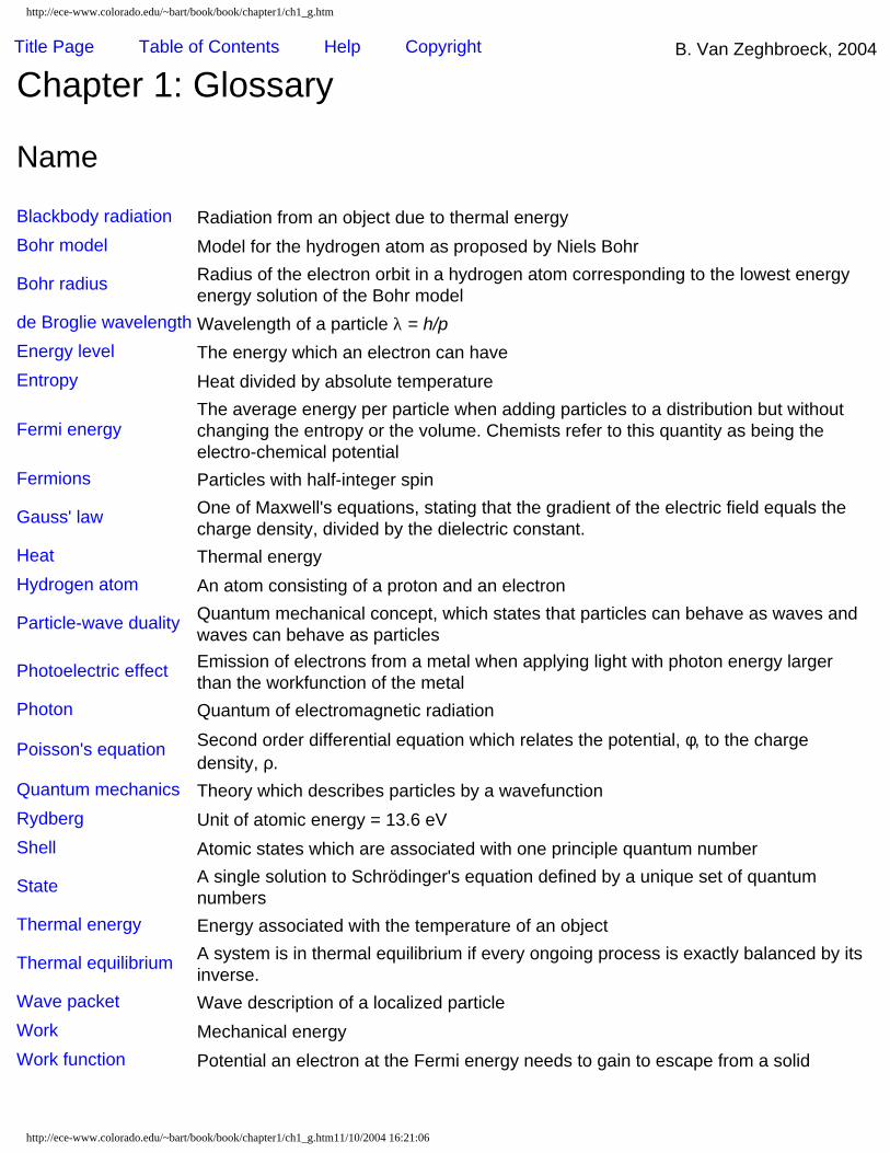
http://ece-www.colorado.edu/~bart/book/book/chapter1/ch1_g.htm
Title Page Table of Contents Help Copyright B. Van Zeghbroeck, 2004
Chapter 1: Glossary
Name
Blackbody radiation Radiation from an object due to thermal energyBohr model Model for the hydrogen atom as proposed by Niels Bohr
Bohr radius Radius of the electron orbit in a hydrogen atom corresponding to the lowest energy energy solution of the Bohr model
de Broglie wavelength Wavelength of a particle λ = h/pEnergy level The energy which an electron can have Entropy Heat divided by absolute temperature
Fermi energyThe average energy per particle when adding particles to a distribution but without changing the entropy or the volume. Chemists refer to this quantity as being the electro-chemical potential
Fermions Particles with half-integer spin
Gauss' law One of Maxwell's equations, stating that the gradient of the electric field equals the charge density, divided by the dielectric constant.
Heat Thermal energyHydrogen atom An atom consisting of a proton and an electron
Particle-wave duality Quantum mechanical concept, which states that particles can behave as waves and waves can behave as particles
Photoelectric effect Emission of electrons from a metal when applying light with photon energy larger than the workfunction of the metal
Photon Quantum of electromagnetic radiation
Poisson's equation Second order differential equation which relates the potential, φ, to the charge density, ρ.
Quantum mechanics Theory which describes particles by a wavefunctionRydberg Unit of atomic energy = 13.6 eVShell Atomic states which are associated with one principle quantum number
State A single solution to Schrödinger's equation defined by a unique set of quantum numbers
Thermal energy Energy associated with the temperature of an object
Thermal equilibrium A system is in thermal equilibrium if every ongoing process is exactly balanced by its inverse.
Wave packet Wave description of a localized particleWork Mechanical energyWork function Potential an electron at the Fermi energy needs to gain to escape from a solid
http://ece-www.colorado.edu/~bart/book/book/chapter1/ch1_g.htm11/10/2004 16:21:06
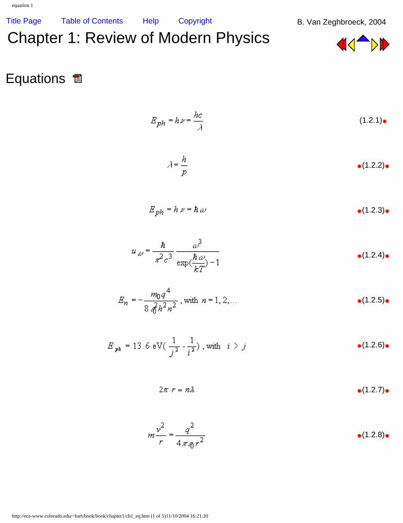
equation 1
Title Page Table of Contents Help Copyright B. Van Zeghbroeck, 2004
Chapter 1: Review of Modern Physics
Equations
(1.2.1)
(1.2.2)
(1.2.3)
(1.2.4)
(1.2.5)
(1.2.6)
(1.2.7)
(1.2.8)
http://ece-www.colorado.edu/~bart/book/book/chapter1/ch1_eq.htm (1 of 5)11/10/2004 16:21:20

equation 1
(1.2.9)
(1.2.10)
(1.2.11)
(1.2.12)
(1.2.13)
(1.2.14)
(1.2.15)
(1.2.16)
(1.2.17)
(1.2.18)
http://ece-www.colorado.edu/~bart/book/book/chapter1/ch1_eq.htm (2 of 5)11/10/2004 16:21:20
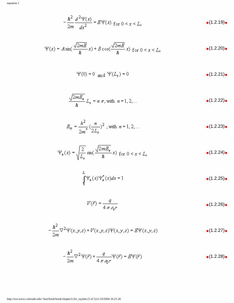
equation 1
(1.2.19)
(1.2.20)
(1.2.21)
(1.2.22)
(1.2.23)
(1.2.24)
(1.2.25)
(1.2.26)
(1.2.27)
(1.2.28)
http://ece-www.colorado.edu/~bart/book/book/chapter1/ch1_eq.htm (3 of 5)11/10/2004 16:21:20
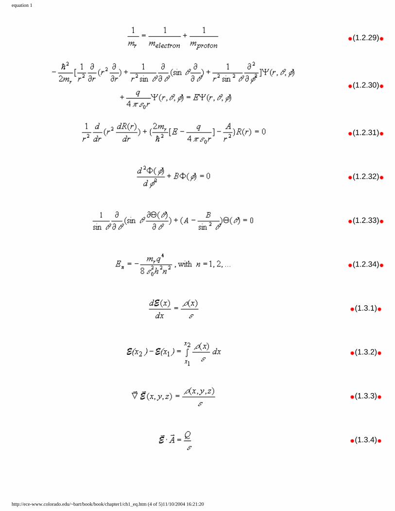
equation 1
(1.2.29)
(1.2.30)
(1.2.31)
(1.2.32)
(1.2.33)
(1.2.34)
(1.3.1)
(1.3.2)
(1.3.3)
(1.3.4)
http://ece-www.colorado.edu/~bart/book/book/chapter1/ch1_eq.htm (4 of 5)11/10/2004 16:21:20
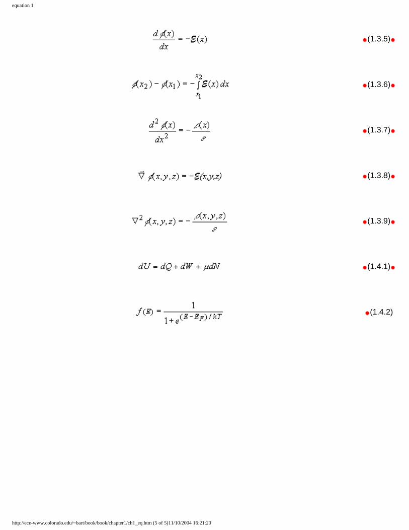
equation 1
(1.3.5)
(1.3.6)
(1.3.7)
(1.3.8)
(1.3.9)
(1.4.1)
(1.4.2)
http://ece-www.colorado.edu/~bart/book/book/chapter1/ch1_eq.htm (5 of 5)11/10/2004 16:21:20

Semiconductor Fundamentals
Title Page Table of Contents Help Copyright B. Van Zeghbroeck, 2004
Chapter 2: Semiconductor Fundamentals
2.1 Introduction
To understand the fundamental concepts of semiconductors, one must apply modern physics to solid materials. More specifically, we are interested in semiconductor crystals. Crystals are solid materials consisting of atoms, which are placed in a highly ordered structure called a lattice. Such a structure yields a periodic potential throughout the material. Two properties of crystals are of particular interest, since they are needed to calculate the current in a semiconductor. First, we need to know how many fixed and mobile charges are present in the material. Second, we need to understand the transport of the mobile carriers through the semiconductor.In this chapter we start from the atomic structure of semiconductors and explain the concepts of energy band gaps, energy bands and the density of states in an energy band. We also show how the current in an almost filled band can more easily be analyzed using the concept of holes. Next, we discuss the probability that energy levels within an energy band are occupied. We will use this probability density to find the density of electrons and holes in a band. Two transport mechanisms will be considered. The drift of carriers in an electric field and the diffusion of carriers due to a carrier density gradient will be discussed. Recombination mechanisms and the continuity equations are then combined into the diffusion equation. Finally, we present the drift-diffusion model, which combines all the essential elements discussed in this chapter.
http://ece-www.colorado.edu/~bart/book/book/chapter2/ch2_1.htm11/10/2004 16:21:54

Semiconductor Fundamentals
Title Page Table of Contents Help Copyright B. Van Zeghbroeck, 2004
Chapter 2: Semiconductor Fundamentals
2.2. Crystals and crystal structures2.2.1. Bravais lattices2.2.2. Common semiconductor crystal structures2.2.3. Growth of semiconductor crystals
Solid materials are classified by the way the atoms are arranged within the solid. Materials in which atoms are placed randomly are called amorphous. Materials in which atoms are placed in a high ordered structure are called crystalline. Poly-crystalline materials are materials with a high degree of short-range order and no long-range order. These materials consist of small crystalline regions with random orientation called grains, separated by grain boundaries.Of primary interest in this text are crystalline semiconductors in which atoms are placed in a highly ordered structure. Crystals are categorized by their crystal structure and the underlying lattice. While some crystals have a single atom placed at each lattice point, most crystals have a combination of atoms associated with each lattice point. This combination of atoms is also called the basis.The classification of lattices, the common semiconductor crystal structures and the growth of single-crystal semiconductors are discussed in the following sections.
2.2.1 Bravais lattices
The Bravais lattices are the distinct lattice types, which when repeated can fill the whole space. The lattice can
therefore be generated by three unit vectors, and a set of integers k, l and m so that each lattice point, identified by a vector , can be obtained from:
(2.2.1)
The construction of the lattice points based on a set of unit vectors is illustrated by Figure 2.2.1.
http://ece-www.colorado.edu/~bart/book/book/chapter2/ch2_2.htm (1 of 7)11/10/2004 16:22:21

Semiconductor Fundamentals
Figure 2.2.1: The construction of lattice points using unit vectors In two dimensions, there are five distinct Bravais lattices, while in three dimensions there are fourteen. The lattices in two dimensions are the square lattice, the rectangular lattice, the centered rectangular lattice, the hexagonal lattice and the oblique lattice as shown in Figure 2.2.2. It is customary to organize these lattices in groups which have the same symmetry. An example is the rectangular and the centered rectangular lattice. As can be seen on the figure, all the lattice points of the rectangular lattice can be obtained by a combination of the lattice vectors . The centered rectangular lattice can be constructed in two ways. It can be obtained by starting with the same lattice vectors as those of the rectangular lattice and then adding an additional atom at the center of each rectangle in the lattice. This approach is illustrated by Figure 2.2.2 c). The lattice vectors generate the traditional unit cell and the center atom is obtained by attaching two lattice points to every lattice point of the traditional unit cell. The alternate approach is to define a new set of lattice vectors, one identical to and another starting from the same origin and ending on the center atom. These lattice vectors generate the so-called primitive cell and directly define the centered rectangular lattice.
Figure 2.2.2.: The five Bravais lattices of two-dimensional crystals: (a) cubic, (b) rectangular, (c) centered rectangular, (d) hexagonal and (e) oblique
http://ece-www.colorado.edu/~bart/book/book/chapter2/ch2_2.htm (2 of 7)11/10/2004 16:22:21

Semiconductor Fundamentals
These lattices are listed in Table 2.2.1. a1 and a2 are the magnitudes of the unit vectors and α is the angle between them.
Table 2.2.1.: Bravais lattices of two-dimensional crystalsThe same approach is used for lattices in three dimensions. The fourteen lattices of three-dimensional crystals are classified as shown in Table 2.2.2, where a1, a2 and a3 are the magnitudes of the unit vectors defining the traditional unit cell and α, β and γ are the angles between these unit vectors.
Table 2.2.2.: Bravais lattices of three-dimensional crystalsThe cubic lattices are an important subset of these fourteen Bravais lattices since a large number of semiconductors are cubic. The three cubic Bravais lattices are the simple cubic lattice, the body-centered cubic lattice and the face-centered cubic lattice as shown in Figure 2.2.3. Since all unit vectors identifying the traditional unit cell have the same size, the crystal structure is completely defined by a single number. This number is the lattice constant, a.
http://ece-www.colorado.edu/~bart/book/book/chapter2/ch2_2.htm (3 of 7)11/10/2004 16:22:21

Semiconductor Fundamentals
Figure 2.2.3.: The simple cubic (a), the body-centered cubic (b) and the face centered cubic (c) lattice.
2.2.2 Common semiconductor crystal structures
The most common crystal structure among frequently used semiconductors is the diamond lattice, shown in Figure 2.2.4. Each atom in the diamond lattice has a covalent bond with four adjacent atoms, which together form a tetrahedron. This lattice can also be formed from two face-centered-cubic lattices, which are displaced along the body diagonal of the larger cube in Figure 2.2.4 by one quarter of that body diagonal. The diamond lattice therefore is a face-centered-cubic lattice with a basis containing two identical atoms.
Figure 2.2.4.: The diamond lattice of silicon and germanium Compound semiconductors such as GaAs and InP have a crystal structure that is similar to that of diamond. However, the lattice contains two different types of atoms. Each atom still has four covalent bonds, but they are bonds with atoms of the other type. This structure is referred to as the zinc-blende lattice, named after zinc-blende (ZnS) as shown in Figure 2.2.5. Both the diamond lattice and the zinc-blende lattice are cubic lattices. A third common crystal structure is the hexagonal structure also referred to as the wurzite crystal structure, which is the hexagonal form of zinc sulfide (ZnS).
http://ece-www.colorado.edu/~bart/book/book/chapter2/ch2_2.htm (4 of 7)11/10/2004 16:22:21

Semiconductor Fundamentals
Many semiconductor materials can have more than one crystal structure. A large number of compound semiconductors including GaAs, GaN and ZnS can be either cubic or hexagonal. SiC can be cubic or one of several different hexagonal crystal structures.The cubic crystals are characterized by a single parameter, the lattice constant a, while the hexagonal structures are characterized in the hexagonal plane by a lattice constant a and by the distance between the hexagonal planes, c.
Figure 2.2.5 : The zinc-blende crystal structure of GaAs and InP Example 2.1
Calculate the maximum fraction of the volume in a simple cubic crystal occupied by the atoms. Assume that the atoms are closely packed and that they can be treated as hard spheres. This fraction is also called the packing density.
Solution The atoms in a simple cubic crystal are located at the corners of the units cell, a cube with side a. Adjacent atoms touch each other so that the radius of each atom equals a/2. There are eight atoms occupying the corners of the cube, but only one eighth of each is within the unit cell so that the number of atoms equals one per unit cell. The packing density is then obtained from:
or about half the volume of the unit cell is occupied by the atoms.
The packing density of four cubic crystals is listed in the table below.
http://ece-www.colorado.edu/~bart/book/book/chapter2/ch2_2.htm (5 of 7)11/10/2004 16:22:21
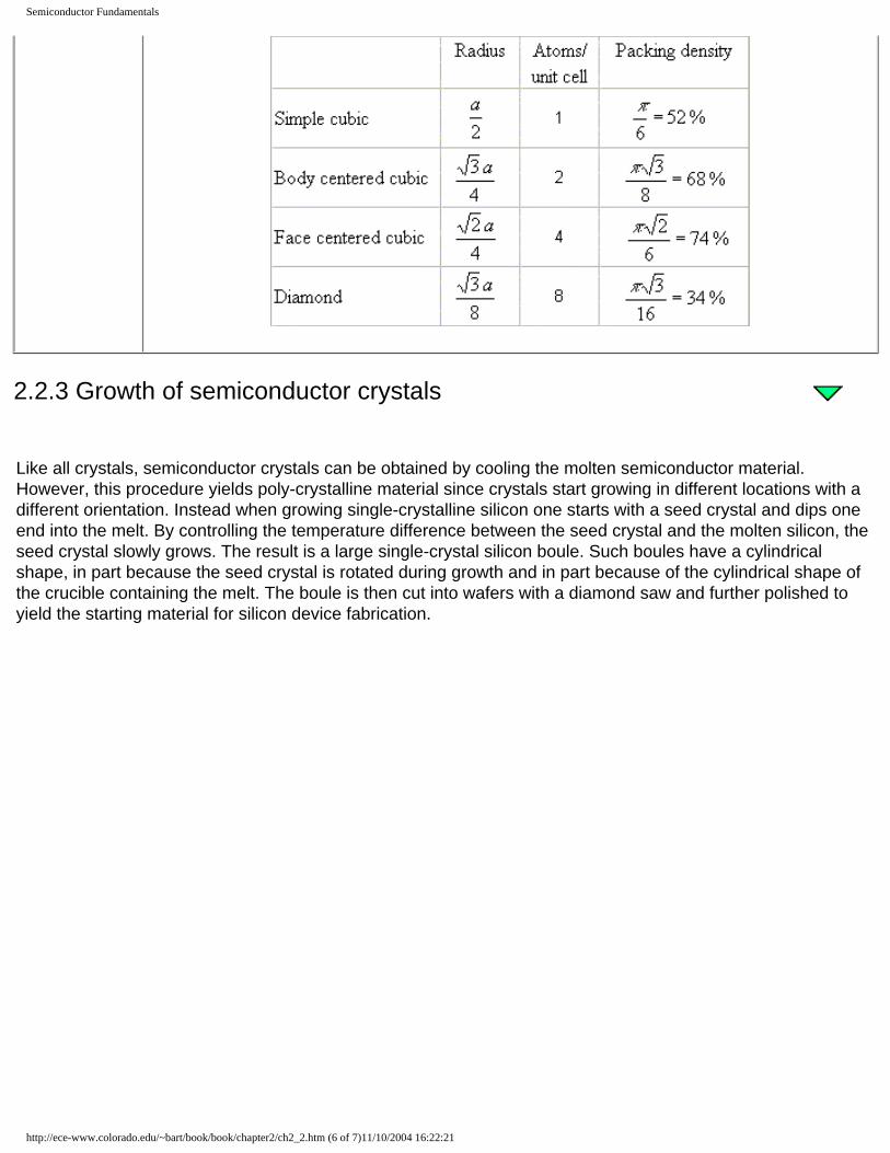
Semiconductor Fundamentals
2.2.3 Growth of semiconductor crystals
Like all crystals, semiconductor crystals can be obtained by cooling the molten semiconductor material. However, this procedure yields poly-crystalline material since crystals start growing in different locations with a different orientation. Instead when growing single-crystalline silicon one starts with a seed crystal and dips one end into the melt. By controlling the temperature difference between the seed crystal and the molten silicon, the seed crystal slowly grows. The result is a large single-crystal silicon boule. Such boules have a cylindrical shape, in part because the seed crystal is rotated during growth and in part because of the cylindrical shape of the crucible containing the melt. The boule is then cut into wafers with a diamond saw and further polished to yield the starting material for silicon device fabrication.
http://ece-www.colorado.edu/~bart/book/book/chapter2/ch2_2.htm (6 of 7)11/10/2004 16:22:21

Semiconductor Fundamentals
http://ece-www.colorado.edu/~bart/book/book/chapter2/ch2_2.htm (7 of 7)11/10/2004 16:22:21

Energy bands
Title Page Table of Contents Help Copyright B. Van Zeghbroeck, 2004
Chapter 2: Semiconductor Fundamentals
2.3 Energy bands2.3.1. Free electron model2.3.2. Periodic potentials2.3.3. Energy bands of semiconductors2.3.4. Metals, insulators and semiconductors2.3.5. Electrons and holes in semiconductors2.3.6. The effective mass concept2.3.7. Detailed description of the effective mass concept
Energy bands consisting of a large number of closely spaced energy levels exist in crystalline materials. The bands can be thought of as the collection of the individual energy levels of electrons surrounding each atom. The wavefunctions of the individual electrons, however, overlap with those of electrons confined to neighboring atoms. The Pauli exclusion principle does not allow the electron energy levels to be the same so that one obtains a set of closely spaced energy levels, forming an energy band. The energy band model is crucial to any detailed treatment of semiconductor devices. It provides the framework needed to understand the concept of an energy bandgap and that of conduction in an almost filled band as described by the empty states.
2.3.1 Free electron model
The free electron model of metals has been used to explain the photo-electric effect (see section 1.2.2). This model assumes that electrons are free to move within the metal but are confined to the metal by potential barriers as illustrated by Figure 2.3.1. The minimum energy needed to extract an electron from the metal equals qΦM, where ΦM is the workfunction. This model is frequently used when analyzing metals. However, this model does not work well for semiconductors since the effect of the periodic potential due to the atoms in the crystal has been ignored.
http://ece-www.colorado.edu/~bart/book/book/chapter2/ch2_3.htm (1 of 11)11/10/2004 16:22:52

Energy bands
Figure 2.3.1.: The free electron model of a metal.
2.3.2 Periodic potentials
The analysis of periodic potentials is required to find the energy levels in a semiconductor. This requires the use of periodic wave functions, called Bloch functions which are beyond the scope of this text. The result of this analysis is that the energy levels are grouped in bands, separated by energy band gaps. The behavior of electrons at the top and bottom of such a band is similar to that of a free electron. However, the electrons are affected by the presence of the periodic potential. The combined effect of the periodic potential is included by adjusting the mass of the electron to a different value. This mass will be referred to as the effective mass.The effect of a periodic arrangement on the electron energy levels is illustrated by Figure 2.3.2. Shown are the energy levels of electrons in a carbon crystal with the atoms arranged in a diamond lattice. These energy levels are plotted as a function of the lattice constant, a.
http://ece-www.colorado.edu/~bart/book/book/chapter2/ch2_3.htm (2 of 11)11/10/2004 16:22:52

Energy bands
Figure 2.3.2. : Energy bands for diamond versus lattice constant . One atomic unit equals 1 Rydberg = 13.6 eV.
Isolated carbon atoms contain six electrons, which occupy the 1s, 2s and 2p orbital in pairs. The energy of an electron occupying the 2s and 2p orbital is indicated on the figure. The energy of the 1s orbital is not shown. As the lattice constant is reduced, there is an overlap of the electron wavefunctions occupying adjacent atoms. This leads to a splitting of the energy levels consistent with the Pauli exclusion principle. The splitting results in an energy band containing 2N states in the 2s band and 6N states in the 2p band, where N is the number of atoms in the crystal. A further reduction of the lattice constant causes the 2s and 2p energy bands to merge and split again into two bands containing 4N states each. At zero Kelvin, the lower band is completely filled with electrons and labeled as the valence band. The upper band is empty and labeled as the conduction band.
2.3.3 Energy bands of semiconductors
2.3.3.1. Energy band diagrams of common semiconductors2.3.3.2. Simple energy band diagram of a semiconductor2.3.3.3. Temperature dependence of the energy bandgap
Complete energy band diagrams of semiconductors are very complex. However, most have features similar to that of the diamond crystal discussed in section 2.3.2. In this section, we first take a closer look at the energy band diagrams of common semiconductors. We then present a simple diagram containing some of the most important feature and discuss the temperature dependence of the energy bandgap.
2.3.3.1. Energy band diagrams of common semiconductors
The energy band diagrams of semiconductors are rather complex. The detailed energy band diagrams of germanium, silicon and gallium arsenide are shown in Figure 2.3.3. The energy is plotted as a function of the wavenumber, k, along the main crystallographic directions in the crystal, since the band diagram depends on the direction in the crystal. The energy band diagrams contain multiple completely-filled and completely-empty bands. In addition, there are multiple partially-filled band.
http://ece-www.colorado.edu/~bart/book/book/chapter2/ch2_3.htm (3 of 11)11/10/2004 16:22:52

Energy bands
Figure 2.3.3.: Energy band diagram of (a) germanium, (b) silicon and (c) gallium arsenideFortunately, we can simplify the energy band diagram since only the electrons in the highest almost-filled band and the lowest almost-empty band dominate the behavior of the semiconductor. These bands are indicated on the figure by the + and - signs corresponding to the charge of the carriers in those bands.
2.3.3.2. Simple energy band diagram of a semiconductor
The energy band diagrams shown in the previous section are frequently simplified when analyzing semiconductor devices. Since the electronic properties of a semiconductor are dominated by the highest partially empty band and the lowest partially filled band, it is often sufficient to only consider those bands. This leads to a simplified energy band diagram for semiconductors as shown in Figure 2.3.4:
http://ece-www.colorado.edu/~bart/book/book/chapter2/ch2_3.htm (4 of 11)11/10/2004 16:22:52

Energy bands
Figure 2.3.4.: A simplified energy band diagram used to describe semiconductors. Shown are the valence and conduction band as indicated by the valence band edge, Ev, and the conduction band edge, Ec. The vacuum level, Evacuum, and the electron affinity, χ, are also indicated on the figure.
The diagram identifies the almost-empty conduction band by a horizontal line. This line indicates the bottom edge of the conduction band and is labeled Ec. Similarly, the top of the valence band is indicated by a horizontal line labeled Ev. The energy band gap is located between the two lines, which are separated by the bandgap energy Eg. The distance between the conduction band edge, Ec, and the energy of a free electron outside the crystal (called the vacuum level labeled Evacuum) is quantified by the electron affinity, χ multiplied with the electronic charge q.An important feature of an energy band diagram, which is not included on the simplified diagram, is whether the conduction band minimum and the valence band maximum occur at the same value for the wavenumber. If so, the energy bandgap is called direct. If not, the energy bandgap is called indirect. This distinction is of interest for optoelectronic devices as direct bandgap materials provide more efficient absorption and emission of light. For instance, the smallest bandgap of germanium and silicon is indirect, while gallium arsenide has a direct bandgap as can be seen on Figure 2.3.3.
2.3.3.3. Temperature dependence of the energy bandgap
The energy bandgap of semiconductors tends to decrease as the temperature is increased. This behavior can be better understood if one considers that the interatomic spacing increases when the amplitude of the atomic vibrations increases due to the increased thermal energy. This effect is quantified by the linear expansion coefficient of a material. An increased interatomic spacing decreases the average potential seen by the electrons in the material, which in turn reduces the size of the energy bandgap. A direct modulation of the interatomic distance - such as by applying compressive (tensile) stress - also causes an increase (decrease) of the bandgap.
http://ece-www.colorado.edu/~bart/book/book/chapter2/ch2_3.htm (5 of 11)11/10/2004 16:22:52

Energy bands
The temperature dependence of the energy bandgap, Eg, has been experimentally determined yielding the following expression for Eg as a function of the temperature, T:
(2.3.1)
where Eg(0), α and β are the fitting parameters. These fitting parameters are listed for germanium, silicon and gallium arsenide in Table 2.3.1:
Table 2.3.1.: Parameters used to calculate the energy bandgap of germanium, silicon and gallium arsenide (GaAs) as a function of temperature
A plot of the resulting bandgap versus temperature is shown in Figure 2.3.5 for germanium, silicon and gallium arsenide.
Figure 2.3.5.: Temperature dependence of the energy bandgap of germanium (Ge), silicon (Si) and gallium arsenide (GaAs).
Example 2.2. Calculate the energy bandgap of germanium, silicon and gallium arsenide at 300, 400, 500 and 600 K.
http://ece-www.colorado.edu/~bart/book/book/chapter2/ch2_3.htm (6 of 11)11/10/2004 16:22:52
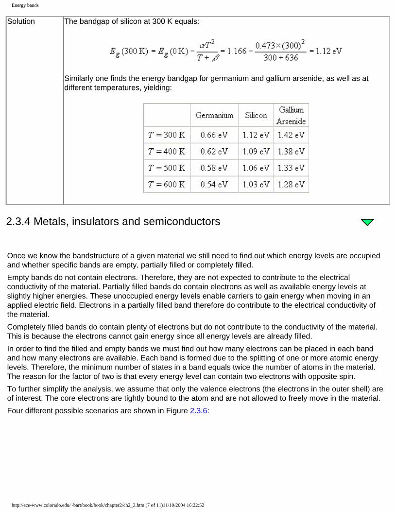
Energy bands
Solution The bandgap of silicon at 300 K equals:
Similarly one finds the energy bandgap for germanium and gallium arsenide, as well as at different temperatures, yielding:
2.3.4 Metals, insulators and semiconductors
Once we know the bandstructure of a given material we still need to find out which energy levels are occupied and whether specific bands are empty, partially filled or completely filled. Empty bands do not contain electrons. Therefore, they are not expected to contribute to the electrical conductivity of the material. Partially filled bands do contain electrons as well as available energy levels at slightly higher energies. These unoccupied energy levels enable carriers to gain energy when moving in an applied electric field. Electrons in a partially filled band therefore do contribute to the electrical conductivity of the material. Completely filled bands do contain plenty of electrons but do not contribute to the conductivity of the material. This is because the electrons cannot gain energy since all energy levels are already filled. In order to find the filled and empty bands we must find out how many electrons can be placed in each band and how many electrons are available. Each band is formed due to the splitting of one or more atomic energy levels. Therefore, the minimum number of states in a band equals twice the number of atoms in the material. The reason for the factor of two is that every energy level can contain two electrons with opposite spin. To further simplify the analysis, we assume that only the valence electrons (the electrons in the outer shell) are of interest. The core electrons are tightly bound to the atom and are not allowed to freely move in the material. Four different possible scenarios are shown in Figure 2.3.6:
http://ece-www.colorado.edu/~bart/book/book/chapter2/ch2_3.htm (7 of 11)11/10/2004 16:22:52

Energy bands
Figure 2.3.6.: Possible energy band diagrams of a crystal. Shown are a) a half filled band, b) two overlapping bands, c) an almost full band separated by a small bandgap from an almost empty band and d) a full band and an empty band separated by a large bandgap.
A half-filled band is shown in Figure 2.3.6 a). This situation occurs in materials consisting of atoms, which contain only one valence electron per atom. Most highly conducting metals including copper, gold and silver satisfy this condition. Materials consisting of atoms that contain two valence electrons can still be highly conducting if the resulting filled band overlaps with an empty band. This scenario is shown in b). No conduction is expected for scenario d) where a completely filled band is separated from the next higher empty band by a larger energy gap. Such materials behave as insulators. Finally, scenario c) depicts the situation in a semiconductor. The completely filled band is now close enough to the next higher empty band that electrons can make it into the next higher band. This yields an almost full band below an almost empty band. We will call the almost full band the valence band since it is occupied by valence electrons. The almost empty band will be called the conduction band, as electrons are free to move in this band and contribute to the conduction of the material.
2.3.5 Electrons and holes in semiconductors
As pointed out in section 2.3.4, semiconductors differ from metals and insulators by the fact that they contain an "almost-empty" conduction band and an "almost-full" valence band. This also means that we will have to deal with the transport of carriers in both bands. To facilitate the discussion of the transport in the "almost-full" valence band of a semiconductor, we will introduce the concept of holes. It is important for the reader to understand that one could deal with only electrons if one is willing to keep track of all the electrons in the "almost-full" valence band. After all, electrons are the only real particles available in a semiconductor.The concepts of holes is introduced in semiconductors since it is easier to keep track of the missing electrons in an "almost-full" band, rather than keeping track of the actual electrons in that band. We will now first explain the concept of a hole and then point out how the hole concept simplifies the analysis. Holes are missing electrons. They behave as particles with the same properties as the electrons would have when occupying the same states except that they carry a positive charge. This definition is illustrated further with Figure 2.3.7, which presents the energy band diagram in the presence of an electric field.
http://ece-www.colorado.edu/~bart/book/book/chapter2/ch2_3.htm (8 of 11)11/10/2004 16:22:52
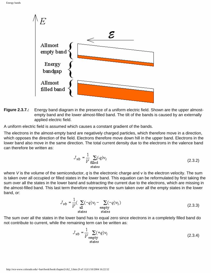
Energy bands
Figure 2.3.7.: Energy band diagram in the presence of a uniform electric field. Shown are the upper almost-empty band and the lower almost-filled band. The tilt of the bands is caused by an externally applied electric field.
A uniform electric field is assumed which causes a constant gradient of the bands.The electrons in the almost-empty band are negatively charged particles, which therefore move in a direction, which opposes the direction of the field. Electrons therefore move down hill in the upper band. Electrons in the lower band also move in the same direction. The total current density due to the electrons in the valence band can therefore be written as:
(2.3.2)
where V is the volume of the semiconductor, q is the electronic charge and v is the electron velocity. The sum is taken over all occupied or filled states in the lower band. This equation can be reformulated by first taking the sum over all the states in the lower band and subtracting the current due to the electrons, which are missing in the almost-filled band. This last term therefore represents the sum taken over all the empty states in the lower band, or:
(2.3.3)
The sum over all the states in the lower band has to equal zero since electrons in a completely filled band do not contribute to current, while the remaining term can be written as:
(2.3.4)
http://ece-www.colorado.edu/~bart/book/book/chapter2/ch2_3.htm (9 of 11)11/10/2004 16:22:52

Energy bands
which states that the current is due to positively charged particles associated with the empty states in the almost-filled band. We call these particles holes. Keep in mind that there is no real particle associated with a hole. Instead, the combined behavior of all the electrons, which occupy states in the almost-filled band, is the same as that of positively charge particles associated with the unoccupied states. The reason the concept of holes simplifies the analysis is that the density of states function of a whole band can be rather complex. However, it can be dramatically simplified if only states close to the band edge need to be considered.
2.3.6 The effective mass concept
Electrons with an energy close to a band minimum behave as free electrons. They accelerate in an applied electric field just like a free electron in vacuum. Their wavefunctions are periodic and extend over the size of the material. The presence of the periodic potential, due to the atoms in the crystal without the valence electrons, changes the properties of the electrons. Therefore, the mass of the electron differs from the free electron mass, m0. Because of the anisotropy of the effective mass and the presence of multiple equivalent band minima, we define two types of effective mass, the effective mass for density of states calculations and the effective mass for conductivity calculations. The effective mass values for electrons and holes are listed together with the value of the smallest energy bandgap in Table 2.3.2. Electrons in gallium arsenide have an isotropic effective mass so that the conductivity effective mass equals the density of states effective mass.
Table 2.3.2.: Effective mass of carriers in germanium, silicon and gallium arsenide (GaAs)
http://ece-www.colorado.edu/~bart/book/book/chapter2/ch2_3.htm (10 of 11)11/10/2004 16:22:52

Energy bands
http://ece-www.colorado.edu/~bart/book/book/chapter2/ch2_3.htm (11 of 11)11/10/2004 16:22:52

2.3.7. The effective mass: detailed description
2.3.7.1. Introduction
The effective mass of a semiconductor is obtained by fitting the actual E-k diagram around the conduction band minimum or the valence band maximum by a paraboloid. While this concept is simple enough, the issue turns out to be substantially more complex due to the multitude and the occasional anisotropy of the minima and maxima. In this section we first describe the different relevant band minima and maxima, present the numeric values for germanium, silicon and gallium arsenide and introduce the effective mass for density of states calculations and the effective mass for conductivity calculations.
Most semiconductors can be described as having one band minimum at k = 0 as well as several equivalent anisotropic band minima at k ≠ 0. In addition there are three band maxima of interest close to the valence band edge.
2.3.7.2.Band structure of silicon
As an example we consider the band structure of silicon as shown in the figure below:
Figure 2.3.8 Simplified E-k diagram of silicon.
Shown is the E-k diagram within the first brillouin zone and along the (100) direction. The energy is chosen to be to zero at the edge of the valence band. The lowest band minimum at k = 0 and still above the valence band edge occurs at Ec,direct = 3.2 eV. This is not the lowest minimum above the valence band edge since there are also 6 equivalent minima at k = (x,0,0), (-x,0,0), (0,x,0), (0,-x,0), (0,0,x), and (0,0,-x) with x = 5 nm-1. The minimum energy of all these minima equals 1.12 eV = Ec,indirect. The effective mass of these anisotropic minima is characterized by a longitudinal mass along the corresponding equivalent (100) direction and two
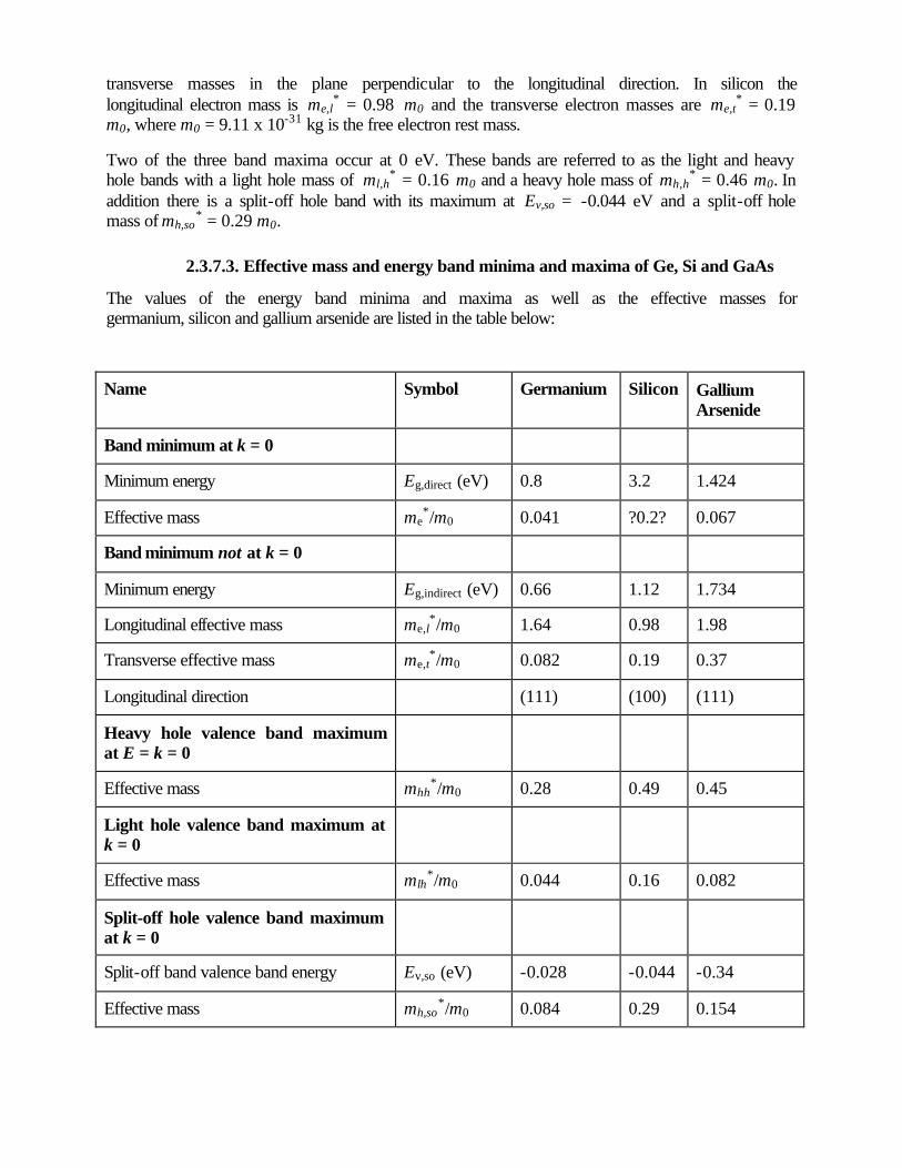
transverse masses in the plane perpendicular to the longitudinal direction. In silicon the longitudinal electron mass is me,l
* = 0.98 m0 and the transverse electron masses are me,t* = 0.19
m0, where m0 = 9.11 x 10⁻³¹ kg is the free electron rest mass.
Two of the three band maxima occur at 0 eV. These bands are referred to as the light and heavy hole bands with a light hole mass of ml,h
* = 0.16 m0 and a heavy hole mass of mh,h* = 0.46 m0. In
addition there is a split-off hole band with its maximum at Ev,so = -0.044 eV and a split-off hole mass of mh,so
* = 0.29 m0.
2.3.7.3. Effective mass and energy band minima and maxima of Ge, Si and GaAs
The values of the energy band minima and maxima as well as the effective masses for germanium, silicon and gallium arsenide are listed in the table below:
Name Symbol Germanium Silicon Gallium Arsenide
Band minimum at k = 0
Minimum energy Eg,direct (eV) 0.8 3.2 1.424
Effective mass me*/m0 0.041 ?0.2? 0.067
Band minimum not at k = 0
Minimum energy Eg,indirect (eV) 0.66 1.12 1.734
Longitudinal effective mass me,l*/m0 1.64 0.98 1.98
Transverse effective mass me,t*/m0 0.082 0.19 0.37
Longitudinal direction (111) (100) (111)
Heavy hole valence band maximum at E = k = 0
Effective mass mhh*/m0 0.28 0.49 0.45
Light hole valence band maximum at k = 0
Effective mass mlh*/m0 0.044 0.16 0.082
Split-off hole valence band maximum at k = 0
Split-off band valence band energy Ev,so (eV) -0.028 -0.044 -0.34
Effective mass mh,so*/m0 0.084 0.29 0.154
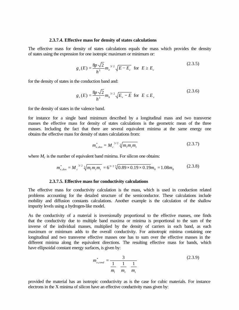
2.3.7.4. Effective mass for density of states calculations
The effective mass for density of states calculations equals the mass which provides the density of states using the expression for one isotropic maximum or minimum or:
ccec EEEEm
hEg ≥−= for
28)( 2/3
3
π
(2.3.5)
for the density of states in the conduction band and:
vvhv EEEEm
hEg ≤−= for
28)( 2/3
3
π
(2.3.6)
for the density of states in the valence band.
for instance for a single band minimum described by a longitudinal mass and two transverse masses the effective mass for density of states calculations is the geometric mean of the three masses. Including the fact that there are several equivalent minima at the same energy one obtains the effective mass for density of states calculations from:
32/3*, ttlcdose mmmMm = (2.3.7)
where Mc is the number of equivalent band minima. For silicon one obtains:
00
32/332/3*, 08.119.019.089.06 mmmmmMm ttlcdose =××== (2.3.8)
2.3.7.5. Effective mass for conductivity calculations
The effective mass for conductivity calculation is the mass, which is used in conduction related problems accounting for the detailed structure of the semiconductor. These calculations include mobility and diffusion constants calculations. Another example is the calculation of the shallow impurity levels using a hydrogen-like model.
As the conductivity of a material is inversionally proportional to the effective masses, one finds that the conductivity due to multiple band maxima or minima is proportional to the sum of the inverse of the individual masses, multiplied by the density of carriers in each band, as each maximum or minimum adds to the overall conductivity. For anisotropic minima containing one longitudinal and two transverse effective masses one has to sum over the effective masses in the different minima along the equivalent directions. The resulting effective mass for bands, which have ellipsoidal constant energy surfaces, is given by:
ttl
conde
mmm
m111
3*,
++=
(2.3.9)
provided the material has an isotropic conductivity as is the case for cubic materials. For instance electrons in the X minima of silicon have an effective conductivity mass given by:

0
*, 26.0
19.01
19.01
89.01
3111
3m
mmm
m
ttl
conde =++
=++
= (2.3.10)
2.3.7.6.Effective mass and energy bandgap of Ge, Si and GaAs
Name Symbol Germanium Silicon Gallium Arsenide
Smallest energy bandgap at 300 K Eg (eV) 0.66 1.12 1.424
Effective mass for density of states calculations
Electrons me*
,dos/m0 0.56 1.08 0.067
Holes mh*
,dos/m0 0.29 0.57/0.812 0.47
Effective mass for conductivity calculations
Electrons me*
,cond/m0 0.12 0.26 0.067
Holes mh*
,cond/m0 0.21 0.36/0.3862 0.34
m0 = 9.11 x 10⁻³¹ kg is the free electron rest mass.
2 Due to the fact that the heavy hole band does not have a spherical symmetry there is a discrepancy between the actual effective mass for density of states and conductivity calculations (number on the right) and the calculated value (number on the left) which is based on spherical constant-energy surfaces. The actual constant-energy surfaces in the heavy hole band are "warped", resembling a cube with rounded corners and dented-in faces.

Density of states
Title Page Table of Contents Help Copyright B. Van Zeghbroeck, 2004
Chapter 2: Semiconductor Fundamentals
2.4 Density of states2.4.1. Calculation of the density of states2.4.2. Calculation of the density of states in 1, 2 and 3 dimensions
Before we can calculate the density of carriers in a semiconductor, we have to find the number of available states at each energy. The number of electrons at each energy is then obtained by multiplying the number of states with the probability that a state is occupied by an electron. Since the number of energy levels is very large and dependent on the size of the semiconductor, we will calculate the number of states per unit energy and per unit volume.
2.4.1 Calculation of the density of states
The density of states in a semiconductor equals the density per unit volume and energy of the number of solutions to Schrödinger's equation. We will assume that the semiconductor can be modeled as an infinite quantum well in which electrons with effective mass, m*, are free to move. The energy in the well is set to zero. The semiconductor is assumed a cube with side L. This assumption does not affect the result since the density of states per unit volume should not depend on the actual size or shape of the semiconductor.The solutions to the wave equation (equation 1.2.14) where V(x) = 0 are sine and cosine functions:
(2.4.1)
Where A and B are to be determined. The wavefunction must be zero at the infinite barriers of the well. At x = 0 the wavefunction must be zero so that only sine functions can be valid solutions or B must equal zero. At x = L, the wavefunction must also be zero yielding the following possible values for the wavenumber, kx.
(2.4.2)
This analysis can now be repeated in the y and z direction. Each possible solution corresponds to a cube in k-space with size nπ/L as indicated on Figure 2.4.1.
http://ece-www.colorado.edu/~bart/book/book/chapter2/ch2_4.htm (1 of 3)11/10/2004 16:23:41

Density of states
Figure 2.4.1: Calculation of the number of states with wavenumber less than k.The total number of solutions with a different value for kx, ky and kz and with a magnitude of the wavevector less than k is obtained by calculating the volume of one eighth of a sphere with radius k and dividing it by the
volume corresponding to a single solution, , yielding:
(2.4.3)
A factor of two is added to account for the two possible spins of each solution. The density per unit energy is then obtained using the chain rule:
(2.4.4)
The kinetic energy E of a particle with mass m* is related to the wavenumber, k, by:
(2.4.5)
And the density of states per unit volume and per unit energy, g(E), becomes:
(2.4.6)
The density of states is zero at the bottom of the well as well as for negative energies.The same analysis also applies to electrons in a semiconductor. The effective mass takes into account the effect of the periodic potential on the electron. The minimum energy of the electron is the energy at the bottom of the conduction band, Ec, so that the density of states for electrons in the conduction band is given by:
(2.4.7)
http://ece-www.colorado.edu/~bart/book/book/chapter2/ch2_4.htm (2 of 3)11/10/2004 16:23:41

Density of states
Example 2.3 Calculate the number of states per unit energy in a 100 by 100 by 10 nm piece of silicon (m* = 1.08 m0) 100 meV above the conduction band edge. Write the result in units of eV-1.
Solution The density of states equals:
So that the total number of states per unit energy equals:
http://ece-www.colorado.edu/~bart/book/book/chapter2/ch2_4.htm (3 of 3)11/10/2004 16:23:41

2.4.2. Calculation of the density of states in 1, 2 and 3 dimensions We will here postulate that the density of electrons in k–space is constant and equals the physical length of the sample divided by 2π and that for each dimension. The number of states between k and k + dk in 3, 2 and 1 dimension then equals:
)
2(22 ,)
2(2 ,4)
2(2 122233
ππ
ππ
πL
dkdN
kL
dkdN
kL
dkdN DDD ===
(2.4.8)
We now assume that the electrons in a semiconductor are close to a band minimum, Emin and can be described as free particles with a constant effective mass, or:
*2
22
min8
)(m
khEkE
π+=
(2.4.9)
Elimination of k using the E(k) relation above then yields the desired density of states functions, namely:
minmin
2/3*3
33, for ,
28EEEEm
hdEdN
g DDc ≥−==
π
(2.4.10)
for a three-dimensional semiconductor,
min2
*2
2, for ,4
EEh
mdE
dNg D
Dc ≥==π
(2.4.11)
For a two-dimensional semiconductor such as a quantum well in which particles are confined to a plane, and
min
min2
*1
1, for ,12
EEEEh
mdE
dNg D
Dc ≥−
==π
(2.4.12)
For a one-dimensional semiconductor such as a quantum wire in which particles are confined along a line.
An example of the density of states in 3, 2 and 1 dimension is shown in the figure below:

Review of Modern Physics 5
Figure 2.4.2 Density of states per unit volume and energy for a 3-D semiconductor (blue curve), a 10 nm quantum well with infinite barriers (red curve) and a 10 nm by 10 nm quantum wire with infinite barriers (green curve). m*/m0 = 0.8.
The above figure illustrates the added complexity of the quantum well and quantum wire: Even though the density in two dimensions is constant, the density of states for a quantum well is a step function with steps occurring at the energy of each quantized level. The case for the quantum wire is further complicated by the degeneracy of the energy levels: for instance a two-fold degeneracy increases the density of states associated with that energy level by a factor of two. A list of the degeneracy (not including spin) for the 10 lowest energies in a quantum well, a quantum wire and a quantum box, all with infinite barriers, is provided in the table below:
Quantum Well Quantum Wire Quantum Box
nx E/E0 Degeneracy nx ny E/E0 Degeneracy nx ny nz E/E0 Degeneracy
1 1 1 1 1 2 1 1 1 1 3 1
2 4 1 1 2 5 2 1 1 2 6 3
3 9 1 2 2 8 1 1 2 2 9 3
4 16 1 1 3 10 2 1 1 3 11 3
5 25 1 2 3 13 2 2 2 2 12 1
6 36 1 1 4 17 2 1 2 3 14 6
7 49 1 3 3 18 1 2 2 3 17 3

8 64 1 2 4 20 2 1 1 4 18 3
9 81 1 3 4 25 2 1 3 3 19 3
10 100 1 1 5 26 2 1 2 4 21 6
11 121 1 2 5 29 2 2 3 3 22 3
12 144 1 4 4 32 1 2 2 4 24 6
13 169 1 3 5 34 2 1 3 4 26 3
14 196 1 1 6 37 6 1 1 5 27 3
15 225 1 2 6 40 13 3 3 3 27 1
3 2 4 29 3
Figure 2.4.3 Degeneracy (not including spin) of the lowest 10 energy levels in a quantum well, a quantum wire with square cross-section and a quantum cube with infinite barriers. The energy E0 equals the lowest energy in a quantum well, which has the same size
Comparison of the number of discreet states in a 3-dimensional cube with the analytic expressions derived above.
Figure 2.4.4 Number of states within a range ∆E = 20 E0 as a function of the normalized energy E/E0. (E0 is the lowest energy in a 1-dimensional quantum well).
The first point corresponds to the number of states.

Review of Modern Physics 7
Figure 2.4.5 Number of states with energy less than or equal to E as a function of E0 (E0 is the lowest energy in an 1-dimensional quantum well).

Carrier distribution functions
Title Page Table of Contents Help Copyright B. Van Zeghbroeck, 2004
Chapter 2: Semiconductor Fundamentals
2.5 Carrier distribution functions2.5.1. Fermi-Dirac distribution function2.5.2. Example2.5.3. Impurity distribution functions2.5.4. Other distribution functions and comparison2.5.5. Derivation of the Fermi-Dirac distribution function
The distribution or probability density functions describe the probability with which one can expect particles to occupy the available energy levels in a given system. Of particular interest is the probability density function of electrons, called the Fermi function. The derivation of such probability density functions belongs in a statistical thermodynamics course. However, given the importance of the Fermi distribution function, we will carefully examine an example as well as the characteristics of this function. Other distribution functions such as the impurity distribution functions, the Bose-Einstein distribution function and the Maxwell Boltzmann distribution are also provided.
2.5.1 Fermi-Dirac distribution function
The Fermi-Dirac distribution function, also called Fermi function, provides the probability of occupancy of energy levels by Fermions. Fermions are half-integer spin particles, which obey the Pauli exclusion principle. The Pauli exclusion principle postulates that only one Fermion can occupy a single quantum state. Therefore, as Fermions are added to an energy band, they will fill the available states in an energy band just like water fills a bucket. The states with the lowest energy are filled first, followed by the next higher ones. At absolute zero temperature (T = 0 K), the energy levels are all filled up to a maximum energy, which we call the Fermi level. No states above the Fermi level are filled. At higher temperature, one finds that the transition between completely filled states and completely empty states is gradual rather than abrupt. Electrons are Fermions. Therefore, the Fermi function provides the probability that an energy level at energy, E, in thermal equilibrium with a large system, is occupied by an electron. The system is characterized by its temperature, T, and its Fermi energy, EF. The Fermi function is given by:
(2.5.1)
This function is plotted in Figure 2.5.1 for different temperatures.
http://ece-www.colorado.edu/~bart/book/book/chapter2/ch2_5.htm (1 of 5)11/10/2004 16:24:36

Carrier distribution functions
Figure 2.5.1 : The Fermi function at three different temperatures.
The Fermi function has a value of one for energies, which are more than a few times kT below the Fermi energy. It equals 1/2 if the energy equals the Fermi energy and decreases exponentially for energies which are a few times kT larger than the Fermi energy. While at T = 0 K the Fermi function equals a step function, the transition is more gradual at finite temperatures and more so at higher temperatures.
2.5.2 Example
To better understand the origin of distribution functions, we now consider a specific system with equidistant energy levels at 0.5, 1.5, 2.5, 3.5, 4.5, 5.5, .... eV. Each energy level can contain two electrons. Since electrons are indistinguishable from each other, no more than two electrons (with opposite spin) can occupy a given energy level. This system contains 20 electrons. The minimum energy of this system corresponds to the situation where all 20 electrons occupy the ten lowest energy levels without placing more than 2 in any given level. This situation occurs at T = 0 K and the total energy equals 100 eV.Since we are interested in a situation where the temperature is not zero, we arbitrarily set the total energy at 106 eV, which is 6 eV more than the minimum possible energy of this system. This ensures that the thermal energy is not zero so that the system must be at a non-zero temperature.There are 24 possible and different configurations, which satisfy these particular constraints. Eight of those configurations are shown in Figure 2.5.2, where the filled circles represent the electrons:
http://ece-www.colorado.edu/~bart/book/book/chapter2/ch2_5.htm (2 of 5)11/10/2004 16:24:36

Carrier distribution functions
Figure 2.5.2 : Eight of the 24 possible configurations in which 20 electrons can be placed having a total energy of 106 eV.
We no apply the basis postulate of statistical thermodynamics, namely that all possible configurations are equally likely to occur. The expected configuration therefore equals the average occupancy of all possible configurations.The average occupancy of each energy level taken over all (and equally probable) 24 configurations is compared in Figure 2.5.3 to the Fermi-Dirac distribution function. A best fit was obtained using a Fermi energy of 9.998 eV and kT = 1.447 eV or T = 16,800 K. The agreement is surprisingly good considering the small size of this system.
Figure 2.5.3 : Probability versus energy averaged over the 24 possible configurations (circles) fitted with a Fermi-Dirac function (solid line) using kT = 1.447 eV and EF = 9.998 eV.
http://ece-www.colorado.edu/~bart/book/book/chapter2/ch2_5.htm (3 of 5)11/10/2004 16:24:36

Carrier distribution functions
Based on the construction of the distribution function in this example, one would expect the distribution function to be dependent on the density of states. This is the case for small systems. However, for large systems and for a single energy level in thermal equilibrium with a larger system, the distribution function no longer depends on the density of states. This is very fortunate, since it dramatically simplifies the carrier density calculations. One should also keep in mind that the Fermi energy for a particular system as obtained in section 2.6 does depend on the density of states.
2.5.3 Impurity distribution functions
The distribution function of impurities differs from the Fermi-Dirac distribution function although the particles involved are Fermions. The difference is due to the fact that an ionized donor energy level still contains one electron, which can have either spin (spin up or spin down). The donor energy level cannot be empty since this would leave a doubly positively charged atom, which would have an energy different from the donor energy. The distribution function for donors therefore differs from the Fermi function and is given by:
(2.5.2)
The distribution function for acceptors differs also because of the different possible ways to occupy the acceptor level. The neutral acceptor contains no electrons. The ionized acceptor contains one electron, which can have either spin, while the doubly negatively charged state is not allowed since this would require a different energy. This restriction would yield a factor of 2 in front of the exponential term. In addition, one finds that most commonly used semiconductors have a two-fold degenerate valence band, which causes this factor to increase to four, yielding:
(2.5.3)
2.5.4 Other distribution functions and comparison
Other distribution functions include the Bose-Einstein distribution and the Maxwell-Boltzmann distribution. These are briefly discussed below and compared to the Fermi-Dirac distribution function.The Bose-Einstein distribution function applies to bosons. Bosons are particles with integer spin and include photons, phonons and a large number of atoms. Bosons do not obey the Pauli exclusion principle so that any number can occupy one energy level. The Bose-Einstein distribution function is given by:
(2.5.4)
This function is only defined for E > EF.
The Maxwell Boltzmann applies to non-interacting particles, which can be distinguished from each other. This distribution function is also called the classical distribution function since it provides the probability of occupancy for non-interacting particles at low densities. Atoms in an ideal gas form a typical example of such particles. The Maxwell-Boltzmann distribution function is given by:
(2.5.5)
http://ece-www.colorado.edu/~bart/book/book/chapter2/ch2_5.htm (4 of 5)11/10/2004 16:24:36

Carrier distribution functions
A plot of the three distribution functions, the Fermi-Dirac distribution, the Maxwell-Boltzmann distribution and the Bose-Einstein distribution is shown in Figure 2.5.4.
Figure 2.5.4 : Probability of occupancy versus energy of the Fermi-Dirac, the Bose-Einstein and the Maxwell-Boltzmann distribution. The Fermi energy, EF, is assumed to be zero.
All three functions are almost equal for large energies (more than a few kT beyond the Fermi energy). The Fermi-Dirac distribution reaches a maximum of 100% for energies, which are a few kT below the Fermi energy, while the Bose-Einstein distribution diverges at the Fermi energy and has no validity for energies below the Fermi energy.
http://ece-www.colorado.edu/~bart/book/book/chapter2/ch2_5.htm (5 of 5)11/10/2004 16:24:36

2.5.5. Derivation of the Fermi-Dirac distribution function
We start from a series of possible energies, labeled Ei. At each energy, we can have gi possible states and the number of states that are occupied equals gifi, where fi is the probability of occupying a state at energy Ei.
The number of possible ways - called configurations - to fit gi fi electrons in gi states, given the restriction that only one electron can occupy each state, equals:
!)!(
!
iiiii
ii fgfgg
gW
−=
(2.5.6)
This equation is obtained by numbering the individual states and exchanging the states rather than the electrons. This yields a total number of gi! possible configurations. However since the empty states are all identical, we need to divide by the number of permutations between the empty states, as all permutations cannot be distinguished from each other and can therefore only be counted once. In addition, all the filled states are indistinguishable from each other, so we need to divide also by all permutations between the filled states, namely gifi!.
The number of possible ways to fit the electrons in the number of available states is called the multiplicity function.
The multiplicity function for the whole system is the product of the multiplicity functions for each energy Ei
∏∏ −
==i iiiii
i
ii fgfgg
gWW
!)!(!
(2.5.7)
Using Stirling’s approximation, one can eliminate the factorial signs, yielding:
[ ]∑∑ −−−−==i
iiiiiiiiiiii
i fgfgfggfgggWW ln)ln()1(lnlnln (2.5.8)
The total number of electrons in the system equals N and the total energy of those N electrons equals E. These system parameters are related to the number of states at each energy, gi, and the probability of occupancy of each state, fi, by:
∑=i
ii fgN (2.5.9)
and
∑=i
iii fgEU (2.5.10)
According to the basic assumption of statistical thermodynamics, all possible configurations are equally probable. The multiplicity function provides the number of configurations for a specific set of occupancy probabilities, fi. The multiplicity function sharply peaks at the thermal equilibrium distribution. The occupancy probability in thermal equilibrium is therefore obtained

by finding the maximum of the multiplicity function, W, while keeping the total energy and the number of electrons constant.
For convenience, we maximize the logarithm of the multiplicity function instead of the multiplicity function itself. According to the Lagrange method of undetermined multipliers, we must maximize the following function:
∑∑ −−j
jjjj
jj fgEbfgaWln (2.5.11)
where a and b need to be determined. The maximum multiplicity function is obtained from:
0ln
)(=
−− ∑∑
jjjj
jjj
iifgEbfgaW
fg∂∂
(2.5.12)
which can be solved, yielding:
0ln =−−
−i
ii
iii bEafg
fgg
(2.5.13)
Or
)exp(1
1)(
iiFDi bEa
Eff++
== (2.5.14)
which can be written in the following form
)exp(1
1)(
βFi
iFD EEEf
−+
= (2.5.15)
with β = 1/b and EF = -a/b. The symbol EF was chosen since this constant has units of energy and will be the constant associated with this probability distribution.
Taking the derivative of the total energy, one obtains:
∑∑ +=i
iiii
iii dEfgfgdEdU )( (2.5.16)
Using the Lagrange equation, this can be rewritten as:
dNEdEfgWddU Fi
iii ++= ∑)(lnβ (2.5.17)
Any variation of the energies, Ei, can only be caused by a change in volume, so that the middle term can be linked to a volume variation dV.

dNEdV
dVdE
fgWddU Fi
iii +
+= ∑)(lnβ
(2.5.18)
Comparing this to the thermodynamic identity:
dNpdVTdSdU µ+−= (2.5.19)
one finds that β = kT and S = k lnW . The energy, EF, equals the energy associated with the particles, namely the lector-chemical potential, µ.
The comparison also identifies the entropy, S, as being the logarithm of the multiplicity function, W, multiplied with Boltzmann’s constant.
The Fermi-Dirac distribution function then becomes:
)exp(1
1)(
kTEE
EfF
FD −+
= (2.5.20)

Carrier densities
Title Page Table of Contents Help Copyright B. Van Zeghbroeck, 2004
Chapter 2: Semiconductor Fundamentals
2.6. Carrier densities2.6.1. General discussion2.6.2. Calculation of the Fermi integral2.6.3. Intrinsic semiconductors2.6.4. Doped semiconductors2.6.5. Non-equilibrium carrier densities
Now that we have discussed the density of states and the distribution functions, we have all the necessary tools to calculate the carrier density in a semiconductor.
2.6.1 General discussion
The density of electrons in a semiconductor is related to the density of available states and the probability that each of these states is occupied. The density of occupied states per unit volume and energy, n(E), is simply the product of the density of states in the conduction band, gc(E) and the Fermi-Dirac probability function, f(E), (also called the Fermi function):
(2.6.1)
Since holes correspond to empty states in the valence band, the probability of having a hole equals the probability that a particular state is not filled, so that the hole density per unit energy, p(E), equals:
(2.6.2)
Where gv(E) is the density of states in the valence band. The density of carriers is then obtained by integrating the density of carriers per unit energy over all possible energies within a band. A general expression is derived as well as an approximate analytic solution, which is valid for non-degenerate semiconductors. In addition, we also present the Joyce-Dixon approximation, an approximate solution useful when describing degenerate semiconductors. The density of states in a semiconductor was obtained by solving the Schrödinger equation for the particles in the semiconductor. Rather than using the actual and very complex potential in the semiconductor, we use the simple particle-in-a box model, where one assumes that the particle is free to move within the material.
For an electron which behaves as a free particle with effective mass, m*, the density of states was derived in section 2.4, yielding:
(2.6.3)
where Ec is the bottom of the conduction band below which the density of states is zero. The density of states for holes in the valence band is given by:
http://ece-www.colorado.edu/~bart/book/book/chapter2/ch2_6.htm (1 of 17)11/10/2004 16:25:11

Carrier densities
(2.6.4)
2.6.2. Calculation of the Fermi integral
2.6.2.1 Carrier density at zero Kelvin2.6.2.2 Non-degenerate semiconductors2.6.2.3 Degenerate semiconductors
The carrier density in a semiconductor, is obtained by integrating the product of the density of states and the probability density function over all possible states. For electrons in the conduction band the integral is taken from the bottom of the conduction band, labeled, Ec, to the top of the conduction band:
(2.6.5)
Where gc(E) is the density of states in the conduction band and f(E) is the Fermi function.
This general expression is illustrated with Figure 2.6.1 for a parabolic density of states function with Ec = 0. The figure shows the density of states function, gc(E), the Fermi function, f(E), as well as the product of both, which is the density of electrons per unit volume and per unit energy, n(E). The integral corresponds to the crosshatched area.
Figure 2.6.1 : The carrier density integral. Shown are the density of states, gc(E), the density per unit energy, n(E), and the probability of occupancy, f(E). The carrier density, no, equals the crosshatched area.
The actual location of the top of the conduction band does not need to be known as the Fermi function goes to zero at higher energies. The upper limit can therefore be replaced by infinity. We also relabeled the carrier density as no to indicate that the carrier density is the carrier density in thermal equilibrium.
http://ece-www.colorado.edu/~bart/book/book/chapter2/ch2_6.htm (2 of 17)11/10/2004 16:25:11
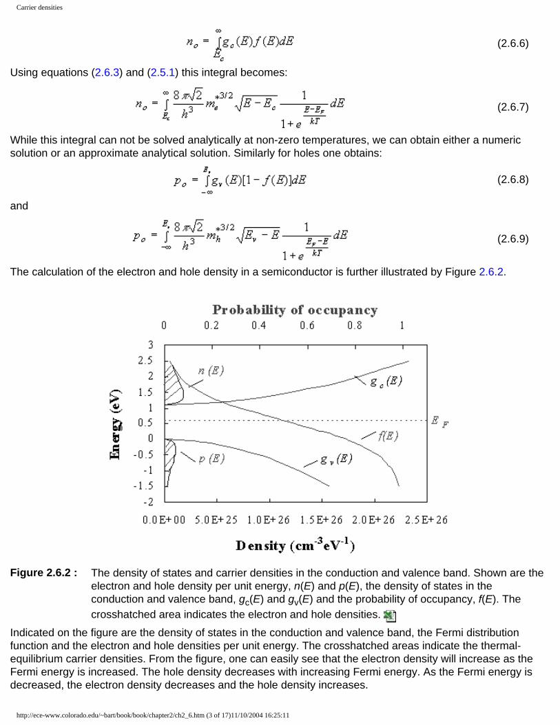
Carrier densities
(2.6.6)
Using equations (2.6.3) and (2.5.1) this integral becomes:
(2.6.7)
While this integral can not be solved analytically at non-zero temperatures, we can obtain either a numeric solution or an approximate analytical solution. Similarly for holes one obtains:
(2.6.8)
and
(2.6.9)
The calculation of the electron and hole density in a semiconductor is further illustrated by Figure 2.6.2.
Figure 2.6.2 : The density of states and carrier densities in the conduction and valence band. Shown are the electron and hole density per unit energy, n(E) and p(E), the density of states in the conduction and valence band, gc(E) and gv(E) and the probability of occupancy, f(E). The crosshatched area indicates the electron and hole densities.
Indicated on the figure are the density of states in the conduction and valence band, the Fermi distribution function and the electron and hole densities per unit energy. The crosshatched areas indicate the thermal-equilibrium carrier densities. From the figure, one can easily see that the electron density will increase as the Fermi energy is increased. The hole density decreases with increasing Fermi energy. As the Fermi energy is decreased, the electron density decreases and the hole density increases.
http://ece-www.colorado.edu/~bart/book/book/chapter2/ch2_6.htm (3 of 17)11/10/2004 16:25:11
Carrier densities
2.6.2.1 Carrier density at zero Kelvin
Equation (2.6.7) can be solved analytically at T = 0 K, since the Fermi function at T = 0 K equals one for all energies below the Fermi energy and 0 for all energies larger than the Fermi energy. Equation (2.6.7) can therefore be simplified to:
(2.6.10)
and integration yields:
(2.6.11)
This expression can be used to approximate the carrier density in heavily degenerate semiconductors provided kT << (EF - Ec) > 0
2.6.2.2 Non-degenerate semiconductors
Non-degenerate semiconductors are defined as semiconductors for which the Fermi energy is at least 3kT away from either band edge. The reason we restrict ourselves to non-degenerate semiconductors is that this definition allows the Fermi function to be replaced by a simple exponential function, i.e. the Maxwell-Boltzmann distribution function. The carrier density integral can then be solved analytically yielding:
(2.6.12)
with
(2.6.13)
where Nc is the effective density of states in the conduction band. Similarly for holes, one can approximate the hole density integral as:
(2.6.14)
with
(2.6.15)
where Nv is the effective density of states in the valence band.
Example 2.4 Calculate the effective densities of states in the conduction and valence bands of germanium, silicon and gallium arsenide at 300 K.
http://ece-www.colorado.edu/~bart/book/book/chapter2/ch2_6.htm (4 of 17)11/10/2004 16:25:11
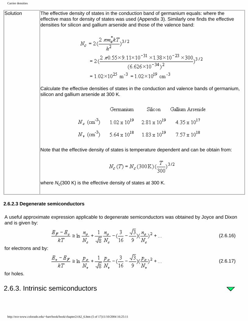
Carrier densities
Solution The effective density of states in the conduction band of germanium equals: where the effective mass for density of states was used (Appendix 3). Similarly one finds the effective densities for silicon and gallium arsenide and those of the valence band:
Calculate the effective densities of states in the conduction and valence bands of germanium, silicon and gallium arsenide at 300 K.
Note that the effective density of states is temperature dependent and can be obtain from:
where Nc(300 K) is the effective density of states at 300 K.
2.6.2.3 Degenerate semiconductors
A useful approximate expression applicable to degenerate semiconductors was obtained by Joyce and Dixon and is given by:
(2.6.16)
for electrons and by:
(2.6.17)
for holes.
2.6.3. Intrinsic semiconductors
http://ece-www.colorado.edu/~bart/book/book/chapter2/ch2_6.htm (5 of 17)11/10/2004 16:25:11

Carrier densities
2.6.3.1 Intrinsic carrier density2.6.3.2 Mass action law2.6.3.3 Intrinsic Fermi energy2.6.3.4 Intrinsic material as reference
Intrinsic semiconductors are semiconductors, which do not contain impurities. They do contain electrons as well as holes. The electron density equals the hole density since the thermal activation of an electron from the valence band to the conduction band yields a free electron in the conduction band as well as a free hole in the valence band. We will identify the intrinsic hole and electron density using the symbol ni, and refer to it as the intrinsic carrier density.
2.6.3.1 Intrinsic carrier density
Intrinsic semiconductors are usually non-degenerate, so that the expressions for the electron (2.6.12) and hole (2.6.14) densities in non-degenerate semiconductors apply. Labeling the Fermi energy of intrinsic material as Ei, we can then write two relations between the intrinsic carrier density and the intrinsic Fermi energy, namely:
(2.6.18)
It is possible to eliminate the intrinsic Fermi energy from both equations, simply by multiplying both equations and taking the square root. This provides an expression for the intrinsic carrier density as a function of the effective density of states in the conduction and valence band, and the bandgap energy Eg = Ec - Ev.
(2.6.19)
The temperature dependence of the intrinsic carrier density is dominated by the exponential dependence on the energy bandgap. In addition, one has to consider the temperature dependence of the effective densities of states and that of the energy bandgap. A plot of the intrinsic carrier density versus temperature is shown in Figure 2.6.3. The temperature dependence of the effective masses was ignored.
Figure 2.6.3 : Intrinsic carrier density versus temperature in gallium arsenide (GaAs), silicon (Si) and germanium (Ge).
http://ece-www.colorado.edu/~bart/book/book/chapter2/ch2_6.htm (6 of 17)11/10/2004 16:25:11

Carrier densities
Example 2.4b Calculate the intrinsic carrier density in germanium, silicon and gallium arsenide at 300, 400, 500 and 600 K.
Solution The intrinsic carrier density in silicon at 300 K equals:
Similarly one finds the intrinsic carrier density for germanium and gallium arsenide at different temperatures, yielding:
Note that the values at 300 K as calculated in example 2.4 are not identical to those listed in Appendix 3. This is due to an accumulation of assumptions in the derivation. The numbers in Appendix 3 are obtained from careful measurements and should therefore be used instead of those calculated in example 2.4.
2.6.3.2 Mass action law
Using the same approach as in section 2.6.3.1, one can prove that the product of the electron and hole density equals the square of the intrinsic carrier density for any non-degenerate semiconductor. By multiplying the expressions for the electron and hole densities in a non-degenerate semiconductor, as in equations (2.6.12) and (2.6.14), one obtains:
(2.6.20)
This property is referred to as the mass action law. It is a powerful relation, which enables to quickly find the hole density if the electron density is known or vice versa. This relation is only valid for non-degenerate semiconductors in thermal equilibrium
2.6.3.3 Intrinsic Fermi energy
The above equations for the intrinsic electron and hole density can be solved for the intrinsic Fermi energy, yielding:
http://ece-www.colorado.edu/~bart/book/book/chapter2/ch2_6.htm (7 of 17)11/10/2004 16:25:11

Carrier densities
(2.6.21)
The intrinsic Fermi energy is typically close to the midgap energy, half way between the conduction and valence band edge. The intrinsic Fermi energy can also be expressed as a function of the effective masses of the electrons and holes in the semiconductor. For this we use equations (2.6.13) and (2.6.15) for the effective density of states in the conduction and valence band, yielding:
(2.6.22)
2.6.3.4 Intrinsic material as reference
Dividing the expressions for the carrier densities (2.6.12) and (2.6.14), by the one for the intrinsic density (2.6.18) allows to write the carrier densities as a function of the intrinsic density, ni, and the intrinsic Fermi energy, Ei, or:
(2.6.23)
and
(2.6.24)
We will use primarily these two equations to find the electron and hole density in a semiconductor in thermal equilibrium. The same relations can also be rewritten to obtain the Fermi energy from either carrier density, namely:
(2.6.25)
and
(2.6.26)
2.6.4. Doped semiconductors
2.6.4.1 Dopants and impurities2.6.4.2 Ionization energy model2.6.4.3 Analysis of non-degenerately doped semiconductors2.6.4.4 General analysis
Doped semiconductors are semiconductors, which contain impurities, foreign atoms incorporated into the crystal structure of the semiconductor. Either these impurities can be unintentional, due to lack of control during the growth of the semiconductor, or they can be added on purpose to provide free carriers in the semiconductor.
http://ece-www.colorado.edu/~bart/book/book/chapter2/ch2_6.htm (8 of 17)11/10/2004 16:25:11

Carrier densities
The generation of free carriers requires not only that impurities are present, but also that the impurities give off electrons to the conduction band in which case they are called donors. If they give off holes to the valence band, they are called acceptors (since they effectively accept an electron from the filled valence band). The ionization of shallow donors and acceptors are illustrated by Figure 2.6.4. Indicated are the donor and acceptor energies, Ed and Ea. The donor energy level is filled prior to ionization. Ionization causes the donor to be emptied, yielding an electron in the conduction band and a positively charged donor ion. The acceptor energy is empty prior to ionization. Ionization of the acceptor corresponds to the empty acceptor level being filled by an electron from the filled valence band. This is equivalent to a hole given off by the acceptor atom to the valence band.
Figure 2.6.4 : Ionization of a) a shallow donor and b) a shallow acceptorA semiconductor doped with impurities, which are ionized (meaning that the impurity atoms either have donated or accepted an electron), will therefore contain free carriers. Shallow impurities are impurities, which require little energy - typically around the thermal energy, kT, or less - to ionize. Deep impurities require energies much larger than the thermal energy to ionize so that only a fraction of the impurities present in the semiconductor contribute to free carriers. Deep impurities, which are more than five times the thermal energy away from either band edge, are very unlikely to ionize. Such impurities can be effective recombination centers, in which electrons and holes fall and annihilate each other. Such deep impurities are also called traps. Ionized donors provide free electrons in a semiconductor, which is then called n-type, while ionized acceptors provide free holes in a semiconductor, which we refer to as being a p-type semiconductor.
2.6.4.1 Dopants and impurities
The ionization of the impurities is dependent on the thermal energy and the position of the impurity level within the energy band gap as described by the impurity distribution functions discussed in section 2.5.3.
Shallow impurities readily ionize so that the free carrier density equals the impurity concentration. For shallow donors this implies that the electron density equals the donor concentration, or:
(2.6.27)
While for shallow acceptors the hole density equals the acceptor concentration, or:
(2.6.28)
http://ece-www.colorado.edu/~bart/book/book/chapter2/ch2_6.htm (9 of 17)11/10/2004 16:25:11

Carrier densities
If a semiconductor contains both shallow donors and shallow acceptors it is called compensated since equal amounts of donor and acceptor atoms compensate each other, yielding no free carriers. The presence of shallow donors and shallow acceptors in a semiconductor cause the electrons given off by the donor atoms to fall into the acceptor state, which ionizes the acceptor atoms without yielding a free electron or hole. The resulting carrier density in compensated material, which contains both shallow donors and shallow acceptors, is approximately equal to the difference between the donor and acceptor concentration if the donor concentration is larger, yielding n-type material, or:
(2.6.29)
If the acceptor concentration is larger than the donor concentration, the hole density of the resulting p-type material equals the difference between the acceptor and donor concentration, or:
(2.6.30)
2.6.4.2 Ionization energy model
The energy required to remove an electron from a donor atom can be approximated using a hydrogen-like model. After all, the donor atom consists of a positively charged ion and an electron just like the proton and electron of the hydrogen atom. The difference however is that the average distance, r, between the electron and the donor ion is much larger since the electron occupies one of the outer orbitals. This is illustrated by Figure 2.6.5.
Figure 2.6.5: Trajectory of an electron bound to a donor ion within a semiconductor crystal.
http://ece-www.colorado.edu/~bart/book/book/chapter2/ch2_6.htm (10 of 17)11/10/2004 16:25:11

Carrier densities
For shallow donors, this distance, r, is much larger than the inter-atomic spacing of the semiconductor crystal. The ionization energy, Ed, can be estimated by modifying equation (1.2.10), which describes the electron energy in a Hydrogen atom, yielding:
(2.6.31)
where m*cond is the effective mass for conductivity calculations and er is the relative dielectric constant of the semiconductor. The ionization energy is calculated as the difference between the energy of a free electron and that of an electron occupying the lowest energy level, E1.
Example 2.5 Calculate the ionization energy for shallow donors and acceptors in germanium and silicon using the hydrogen-like model.
Solution Using the effective mass for conductivity calculations (Appendix 3) one finds the ionization energy for shallow donors in germanium to be:
The calculated ionization energies for donors and acceptors in germanium and silicon are provided below.
Note that the actual ionization energies differ from these values and depend on th actual donor atom.
2.6.4.3 Analysis of non-degenerately doped semiconductors
The calculation of the electron density starts by assuming that the semiconductor is neutral, so that there is a zero charge density in the material. This is a reasonable assumption since a net charge density would result in an electric field. This electric field would move any mobile charge so that it eliminates any charge imbalance. The charge density in a semiconductor depends on the free electron and hole density and on the ionized impurity densities. Ionized donors, which have given off an electron, are positively charged. Ionized acceptors, which have accepted an electron, are negatively charged. The total charge density is therefore given by:
(2.6.32)
The hole concentration in thermal equilibrium can be written as a function of the electron density by using the mass action law (2.6.20). This yields the following relation between the electron density and the ionized impurity densities:
http://ece-www.colorado.edu/~bart/book/book/chapter2/ch2_6.htm (11 of 17)11/10/2004 16:25:11

Carrier densities
(2.6.33)
Note that the use of the mass action law restricts the validity of this derivation to non-degenerate semiconductors as defined in section 2.6.2.2. Solving this quadratic equation yields a solution for the electron density, namely:
(2.6.34)
The same derivation can be repeated for holes, yielding:
(2.6.35)
The above expressions provide the free carrier densities for compensated semiconductors assuming that all donors and acceptors are ionized.From the carrier densities, one then obtains the Fermi energies using equations (2.6.25) and (2.6.26) which are repeated below:
(2.6.25)
or
(2.6.26)
The Fermi energies in n-type and p-type silicon as a function of doping density is shown in Figure 2.6.6 for different temperatures:
http://ece-www.colorado.edu/~bart/book/book/chapter2/ch2_6.htm (12 of 17)11/10/2004 16:25:11

Carrier densities
Figure 2.6.6 : Fermi energy of n-type and p-type silicon, EF,n and EF,p, as a function of doping density at 100, 200, 300, 400 and 500 K. Shown are the conduction and valence band edges, Ec and Ev. The midgap energy is set to zero.
Figure 2.6.6 illustrates how the Fermi energies vary with doping density. The Fermi energy varies linearly, when plotting the density on a logarithmic scale, up to a doping density of 1018 cm-3. This simple dependence requires that the semiconductor is neither intrinsic nor degenerate and that all the dopants are ionized. For compensated material, containing only shallow dopants, one uses the net doping density, |Nd - Na|.
Example 2.6a A germanium wafer is doped with a shallow donor density of 3ni/2. Calculate the electron and hole density.
Solution The electron density is obtained from equation (2.6.34) and the hole density is obtained using the mass action law:
Example 2.6b A silicon wafer is doped with a shallow acceptor doping of 1016 cm-3. Calculate the electron and hole density.
Solution Since the acceptor doping is much larger than the intrinsic density and much smaller than the effective density of states, the hole density equals: The electron density is then obtained using the mass action law The approach described in example 2.6a yields the same result.
2.6.4.4 General analysis
A more general analysis takes also into account the fact that the ionization of the impurities is not 100%, but instead is given by the impurity distribution functions provided in section 2.5.3.
http://ece-www.colorado.edu/~bart/book/book/chapter2/ch2_6.htm (13 of 17)11/10/2004 16:25:11

Carrier densities
The analysis again assumes that there is no net charge in the semiconductor (charge neutrality). This also means that the total density of positively charged particles (holes and ionized donors) must equals the total density of negatively charged particles (electrons and ionized acceptors) yielding:
(2.6.36)
The electron and hole densities are then written as a function of the Fermi energy. For non-degenerate semiconductors one uses equations (2.6.12) and (2.6.14), while the ionized impurity densities equal the impurity density multiplied with the probability of occupancy for the acceptors and one minus the probability of occupancy for the donors. The Joyce-Dixon approximation, described in section 2.6.2.3 is used to calculate the degenerate carrier densities.A graphical solution to equation (2.6.36) above can be obtained by plotting both sides of the equation as a function of the Fermi energy as illustrated in Figure 2.6.7.
Figure 2.6.7 : Graphical solution of the Fermi energy based on the general analysis. The value of the Fermi energy and the free carrier density is obtained at the intersection of the two curves, which represent the total positive and total negative charge in the semiconductor. Na equals 1016 cm-
3 and Nd equals 1014 cm-3.
Figure 2.6.7 shows the positive and negative charge densities as well as the electron and hole densities as a function of the Fermi energy. The dotted lines indicate the position of the acceptor and donor energies. The Fermi energy is obtained at the intersection of both curves as indicated by the arrow.This graphical solution is a very useful tool to explore the Fermi energy as a function of the doping densities, ionization energies and temperature.
http://ece-www.colorado.edu/~bart/book/book/chapter2/ch2_6.htm (14 of 17)11/10/2004 16:25:11

Carrier densities
Operation of devices over a wide temperature range requires a detailed knowledge of the carrier density as a function of temperature. At intermediate temperatures the carrier density approximately equals the net doping, |Na - Nd|. Semiconductors, which satisfy this condition, are also called extrinsic semiconductors. The free carrier density increases at high temperatures for which the intrinsic density approaches the net doping density and decreases at low temperatures due to incomplete ionization of the dopants. The carrier density and Fermi energy are shown in Figure 2.6.8 for silicon doped with 1016 cm-3 donors and 1015 cm-3 acceptors:
Figure 2.6.8 : Electron density and Fermi energy as a function of temperature in silicon with Nd = 1016 cm-3, Na = 1014 cm-3 and Ec - Ed = Ea - Ev = 50 meV. The activation energy at 70 K equals 27.4 meV.
At high temperatures, the carrier density equals the intrinsic carrier concentration, while at low temperatures the carrier density is dominated by the ionization of the donors. The temperature dependence is related to an activation energy by fitting the carrier density versus 1/T on a semi-logarithmic scale to a straight line of the form no(T) = C exp(-EA/kT), where C is a constant. At high temperatures this activation energy equals half the bandgap energy or EA = Eg/2.
The temperature dependence at low temperatures is somewhat more complex as it depends on whether or not the material is compensated. Figure 2.6.8 was calculated for silicon containing both donors and acceptors. At 70 K the electron density is below the donor density but still larger than the acceptor density. Under such conditions the activation energy, EA, equals half of the ionization energy of the donors or (Ec - Ed)/2. At lower temperatures where the electron density is lower than the acceptor density, the activation energy equals the ionization energy or Ec - Ed. This behavior is explained by the fact that the Fermi energy in compensated material is fixed at the donor energy. The donors levels are always partially empty as electrons are removed from the donor atoms to fill the acceptor energy levels. If the acceptor density is smaller than the electron density - as is true for uncompensated material - the Fermi energy does change with temperature and the activation energy approaches half of the ionization energy.
http://ece-www.colorado.edu/~bart/book/book/chapter2/ch2_6.htm (15 of 17)11/10/2004 16:25:11
Carrier densities
Lightly doped semiconductors suffer from freeze-out at relatively high temperature. Higher-doped semiconductors freeze-out at lower temperatures. Highly-doped semiconductors do not contain a single donor energy, but rather an impurity band which overlaps with the conduction or valence band. The overlap of the two bands results in free carriers even at zero Kelvin. Degenerately doping a semiconductor therefore eliminates freeze-out effects.
2.6.5. Non-equilibrium carrier densities
Up until now, we have only considered the thermal equilibrium carrier densities, no and po. However most devices of interest are not in thermal equilibrium. Keep in mind that a constant ambient constant temperature is not a sufficient condition for thermal equilibrium. In fact, applying a non-zero voltage to a device or illuminating it with light will cause a non-equilibrium condition, even if the temperature is constant.To describe a system that is not in thermal equilibrium we assume that each of the carrier distributions is still in equilibrium with itself. Such assumption is justified on the basis that electrons readily interact with each other and interact with holes only on a much longer time scale. As a result the electron density can still be calculated using the Fermi-Dirac distribution function, but with a different value for the Fermi energy. The total carrier density for a non-degenerate semiconductor is then described by:
(2.6.37)
Where δn is the excess electron density and Fn is the quasi-Fermi energy for the electrons. Similarly, the hole density can be expressed as:
(2.6.38)
Where δp is the excess hole density and Fp is the quasi-Fermi energy for the holes.
Example 2.7 A piece of germanium doped with 1016 cm-3 shallow donors is illuminated with light generating 1015 cm-3 excess electrons and holes. Calculate the quasi-Fermi energies relative to the intrinsic energy and compare it to the Fermi energy in the absence of illumination.
Solution The carrier densities when illuminating the semiconductor are:
and the quasi-Fermi energies are:
http://ece-www.colorado.edu/~bart/book/book/chapter2/ch2_6.htm (16 of 17)11/10/2004 16:25:11

Carrier densities
In comparison, the Fermi energy in the absence of light equals
which is very close to the quasi-Fermi energy of the majority carriers.
http://ece-www.colorado.edu/~bart/book/book/chapter2/ch2_6.htm (17 of 17)11/10/2004 16:25:11

Carrier Transport
Title Page Table of Contents Help Copyright B. Van Zeghbroeck, 2004
Chapter 2: Semiconductor Fundamentals
2.7. Carrier Transport2.7.1. Carrier drift2.7.2. Carrier Mobility2.7.3. Velocity saturation2.7.4. Carrier diffusion2.7.5. The Hall effect
A motion of free carriers in a semiconductor leads to a current. This motion can be caused by an electric field due to an externally applied voltage, since the carriers are charged particles. We will refer to this as carrier drift. In addition, carriers also move from regions where the carrier density is high to regions where the carrier density is low. This carrier transport mechanism is due to the thermal energy and the associated random motion of the carriers. We will refer to this transport mechanism as carrier diffusion. The total current in a semiconductor equals the sum of the drift and the diffusion current.As one applies an electric field to a semiconductor, the electrostatic force causes the carriers to first accelerate and then reach a constant average velocity, v, due to collisions with impurities and lattice vibrations. The ratio of the velocity to the applied field is called the mobility. The velocity saturates at high electric fields reaching the saturation velocity. Additional scattering occurs when carriers flow at the surface of a semiconductor, resulting in a lower mobility due to surface or interface scattering mechanisms.Diffusion of carriers is obtained by creating a carrier density gradient. Such gradient can be obtained by varying the doping density in a semiconductor or by applying a thermal gradient.Both carrier transport mechanisms are related since the same particles and scattering mechanisms are involved. This leads to a relationship between the mobility and the diffusion constant called the Einstein relation.
2.7.1. Carrier drift
2.7.1.1 Impurity scattering2.7.1.2 Lattice scattering2.7.1.3 Surface scattering
The motion of a carrier drifting in a semiconductor due to an applied electric field is illustrated in Figure 2.7.1. The field causes the carrier to move with a velocity, v.
http://ece-www.colorado.edu/~bart/book/book/chapter2/ch2_7.htm (1 of 12)11/10/2004 16:25:35

Carrier Transport
Figure 2.7.1 : Drift of a carrier due to an applied electric field.Assuming that all the carriers in the semiconductor move with the same velocity, the current can be expressed as the total charge in the semiconductor divided by the time needed to travel from one electrode to the other, or:
(2.7.1)
where τr is the transit time of a particle, traveling with velocity, v, over the distance L. The current density can then be rewritten as a function of either the charge density, ρ, or the density of carriers, n in the semiconductor:
(2.7.2)
Carriers however do not follow a straight path along the electric field lines, but instead bounce around in the semiconductor and constantly change direction and velocity due to scattering. This behavior occurs even when no electric field is applied and is due to the thermal energy of the electrons. Electrons in a non-degenerate and non-relativistic electron gas have a thermal energy, which equals kT/2 per particle per degree of freedom. A typical thermal velocity at room temperature is around 107 cm/s, which exceeds the typical drift velocity in semiconductors. The carrier motion in the semiconductor in the absence and in the presence of an electric field can therefore be visualized as in Figure 2.7.2.
Figure 2.7.2 : Random motion of carriers in a semiconductor with and without an applied electric field.
http://ece-www.colorado.edu/~bart/book/book/chapter2/ch2_7.htm (2 of 12)11/10/2004 16:25:35
Carrier Transport
In the absence of an applied electric field, the carrier exhibits random motion and the carriers move quickly through the semiconductor and frequently change direction. When an electric field is applied, the random motion still occurs but in addition, there is on average a net motion along the direction of the field.
We now analyze the carrier motion considering only the average velocity, of the carriers. Applying Newton's law, we state that the acceleration of the carriers is proportional to the applied force:
(2.7.3)
The force consists of the difference between the electrostatic force and the scattering force due to the loss of momentum at the time of scattering. This scattering force equals the momentum divided by the average time between scattering events, so that:
(2.7.4)
Combining both relations yields an expression for the average particle velocity:
(2.7.5)
We now consider only the steady state situation in which the particle has already accelerated and has reached a constant average velocity. Under such conditions, the velocity is proportional to the applied electric field and we define the mobility as the velocity to field ratio:
(2.7.6)
The mobility of a particle in a semiconductor is therefore expected to be large if its mass is small and the time between scattering events is large.The drift current, described by (2.7.2), can then be rewritten as a function of the mobility, yielding:
(2.7.7)
Throughout this derivation, we simply considered the mass, m, of the particle. However in order to incorporate the effect of the periodic potential of the atoms in the semiconductor we must use the effective mass, m*, rather than the free particle mass:
(2.7.8)
Example 2.8 Electrons in undoped gallium arsenide have a mobility of 8,800 cm2/V-s. Calculate the average time between collisions. Calculate the distance traveled between two collisions (also called the mean free path). Use an average velocity of 107 cm/s.
http://ece-www.colorado.edu/~bart/book/book/chapter2/ch2_7.htm (3 of 12)11/10/2004 16:25:35

Carrier Transport
Solution The collision time, τc, is obtained from:
where the mobility was first converted in MKS units.
The mean free path, l, equals:
2.7.1.1 Impurity scattering
By impurities, we mean foreign atoms in the solid, which are efficient scattering centers especially when they have a net charge. Ionized donors and acceptors in a semiconductor are a common example of such impurities. The amount of scattering due to electrostatic forces between the carrier and the ionized impurity depends on the interaction time and the number of impurities. Larger impurity concentrations result in a lower mobility. The dependence on the interaction time helps to explain the temperature dependence. The interaction time is directly linked to the relative velocity of the carrier and the impurity, which is related to the thermal velocity of the carriers. This thermal velocity increases with the ambient temperature so that the interaction time increases. Thereby, the amount of scattering decreases, resulting in a mobility increase with temperature. To first order, the mobility due to impurity scattering is proportional to T 3/2/NI, where NI is the density of charged impurities.
2.7.1.2 Lattice scattering
Scattering by lattice waves includes the absorption or emission of either acoustical or optical phonons. Since the density of phonons in a solid increases with temperature, the scattering time due to this mechanism will decrease with temperature as will the mobility. Theoretical calculations reveal that the mobility in non-polar semiconductors, such as silicon and germanium, is dominated by acoustic phonon interaction. The resulting mobility is expected to be proportional to T -3/2, while the mobility due to optical phonon scattering only is expected to be proportional to T -1/2. Experimental values of the temperature dependence of the mobility in germanium, silicon and gallium arsenide are provided in Table 2.7.1.
Table 2.7.1 : Temperature dependence of the mobility in germanium, silicon and gallium arsenide due to phonon scattering
2.7.1.3 Surface scattering
http://ece-www.colorado.edu/~bart/book/book/chapter2/ch2_7.htm (4 of 12)11/10/2004 16:25:35
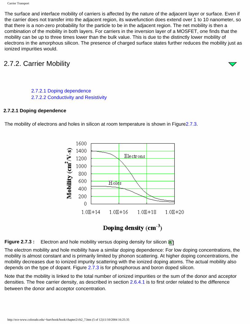
Carrier Transport
The surface and interface mobility of carriers is affected by the nature of the adjacent layer or surface. Even if the carrier does not transfer into the adjacent region, its wavefunction does extend over 1 to 10 nanometer, so that there is a non-zero probability for the particle to be in the adjacent region. The net mobility is then a combination of the mobility in both layers. For carriers in the inversion layer of a MOSFET, one finds that the mobility can be up to three times lower than the bulk value. This is due to the distinctly lower mobility of electrons in the amorphous silicon. The presence of charged surface states further reduces the mobility just as ionized impurities would.
2.7.2. Carrier Mobility
2.7.2.1 Doping dependence2.7.2.2 Conductivity and Resistivity
2.7.2.1 Doping dependence
The mobility of electrons and holes in silicon at room temperature is shown in Figure2.7.3.
Figure 2.7.3 : Electron and hole mobility versus doping density for silicon
The electron mobility and hole mobility have a similar doping dependence: For low doping concentrations, the mobility is almost constant and is primarily limited by phonon scattering. At higher doping concentrations, the mobility decreases due to ionized impurity scattering with the ionized doping atoms. The actual mobility also depends on the type of dopant. Figure 2.7.3 is for phosphorous and boron doped silicon.
Note that the mobility is linked to the total number of ionized impurities or the sum of the donor and acceptor densities. The free carrier density, as described in section 2.6.4.1 is to first order related to the difference between the donor and acceptor concentration.
http://ece-www.colorado.edu/~bart/book/book/chapter2/ch2_7.htm (5 of 12)11/10/2004 16:25:35

Carrier Transport
The minority carrier mobility also depends on the total impurity density. The minority-carrier mobility can be approximated by the majority-carrier mobility in a material with the same number of impurities. The mobility at a particular doping density is obtained from the following empiric expression:
(2.7.9)
Table 2.7.2 : Parameters for calculation of the mobility as a function of the doping density
The resulting mobilities in units of cm2/V-s are listed for different doping densities in Table 2.7.3.
Table 2.7.3 : Mobility in silicon for different doping densities
2.7.2.2 Conductivity and Resistivity
The conductivity of a material is defined as the current density divided by the applied electric field. Since the current density equals the product of the charge of the mobile carriers, their density and velocity, it can be expressed as a function of the electric field using the mobility. To include the contribution of electrons as well as holes to the conductivity, we add the current density due to holes to that of the electrons, or:
(2.7.10)
The conductivity due to electrons and holes is then obtained from:
(2.7.11)
The resistivity is defined as the inverse of the conductivity, namely:
(2.7.12)
The resulting resistivity as calculated with equation (2.7.12) is shown in Figure 2.7.4.
http://ece-www.colorado.edu/~bart/book/book/chapter2/ch2_7.htm (6 of 12)11/10/2004 16:25:35

Carrier Transport
Figure 2.7.4 : Resistivity of n-type and p-type silicon versus doping density
The sheet resistance concept is used to characterize both wafers and thin doped layers, since it is typically easier to measure the sheet resistance rather than the resistivity of the material. The sheet resistance of a uniformly-doped layer with resistivity, r, and thickness, t, is given by their ratio:
(2.7.13)
While the unit of the sheet resistance is Ohms, one refers to it as Ohms per square. This nomenclature comes in handy when the resistance of a rectangular piece of material with length, L, and width W must be obtained. It equals the product of the sheet resistance and the number of squares or:
(2.7.14)
where the number of squares equals the length divided by the width. Figure 2.7.5 provides, as an example, the sheet resistance of a 14 mil thick silicon wafer which is n-type or p-type.
http://ece-www.colorado.edu/~bart/book/book/chapter2/ch2_7.htm (7 of 12)11/10/2004 16:25:35

Carrier Transport
Figure 2.7.5 : Sheet resistance of a 14 mil thick n-type and p-type silicon wafer versus doping density.
Example 2.9 A piece of silicon doped with arsenic (Nd = 1017 cm-3) is 100 µm long, 10 µm wide and 1 µm thick. Calculate the resistance of this sample when contacted one each end.
Solution The resistivity of the silicon equals:
where the mobility was obtained from Table 2.7.3.
The resistance then equals:
An alternate approach is to first calculate the sheet resistance, Rs:
From which one then obtains the resistance:
http://ece-www.colorado.edu/~bart/book/book/chapter2/ch2_7.htm (8 of 12)11/10/2004 16:25:35

Carrier Transport
2.7.3. Velocity saturation
The linear relationship between the average carrier velocity and the applied field breaks down when high fields are applied. As the electric field is increased, the average carrier velocity and the average carrier energy increases as well. When the carrier energy increases beyond the optical phonon energy, the probability of emitting an optical phonon increases abruptly. This mechanism causes the carrier velocity to saturate with increasing electric field. For carriers in silicon and other materials, which do not contain accessible higher bands, the velocity versus field relation can be described by:
(2.7.15)
The maximum obtainable velocity, vsat, is referred to as the saturation velocity.
2.7.4. Carrier diffusion
2.7.4.1 Diffusion current 2.7.4.2 Total current
Carrier diffusion is due to the thermal energy, kT, which causes the carriers to move at random even when no field is applied. This random motion does not yield a net motion of carriers nor does it yield a net current in material with a uniform carrier density as any carrier which leaves a specific location is on average replace by another one. However if a carrier gradient is present, the diffusion process will attempt to make the carrier density uniform: carriers diffuse from regions where the density is high to regions where the density is low. The diffusion process is not unlike the motion of sand on a vibrating table; hills as well as valleys are smoothed out over time. In this section we will first derive the expression for the current due to diffusion and then combine it with the drift current to obtain the total drift-diffusion current.
2.7.4.1 Diffusion current
The derivation is based on the basic notion that carriers at non-zero temperature (Kelvin) have an additional thermal energy, which equals kT/2 per degree of freedom. It is the thermal energy, which drives the diffusion process. At T = 0 K there is no diffusion. While one should recognize that the random nature of the thermal energy would normally require a statistical treatment of the carriers, we instead will use average values to describe the process. Such approach is justified on the basis that a more elaborate statistical approach yields the same results. To further simplify the derivation, we will derive the diffusion current for a one-dimensional semiconductor in which carriers can only move along one direction.
http://ece-www.colorado.edu/~bart/book/book/chapter2/ch2_7.htm (9 of 12)11/10/2004 16:25:35

Carrier Transport
We now introduce the average values of the variables of interest, namely the thermal velocity, vth, the collision time, τc, and the mean free path, l. The thermal velocity is the average velocity of the carriers going in the positive or negative direction. The collision time is the time during which carriers will move with the same velocity before a collision occurs with an atom or with another carrier. The mean free path is the average length a carrier will travel between collisions. These three averages are related by:
(2.7.16)
Consider now the situation illustrated with Figure 2.7.6.
Figure 2.7.6 : Carrier density profile used to derive the diffusion current expressionShown is a variable carrier density, n(x). Of interest are the carrier densities which are one mean free path away from x = 0, since the carriers which will arrive at x = 0 originate either at x = -l or x = l. The flux at x = 0 due to carriers which originate at x = -l and move from left to right equals:
(2.7.17)
where the factor 1/2 is due to the fact that only half of the carriers move to the left while the other half moves to the right. The flux at x = 0 due to carriers, which originate at x = +l and move from right to left, equals:
(2.7.18)
The total flux of carriers moving from left to right at x = 0 therefore equals:
(2.7.19)
Where the flux due to carriers moving from right to left is subtracted from the flux due to carriers moving from left to right. Given that the mean free path is small we can write the difference in densities divided by the distance between x = -l and x = l as the derivative of the carrier density:
(2.7.20)
http://ece-www.colorado.edu/~bart/book/book/chapter2/ch2_7.htm (10 of 12)11/10/2004 16:25:35

Carrier Transport
The electron diffusion current equals this flux times the charge of an electron, or:
(2.7.21)
Typically, we will replace the product of the thermal velocity and the mean free path by a single parameter, namely the diffusion constant, Dn.
(2.7.22)
Repeating the same derivation for holes yields:
(2.7.23)
We now further explore the relation between the diffusion constant and the mobility. At first, it seems that there should be no relation between the two since the driving force is distinctly different: diffusion is caused by thermal energy while an externally applied field causes drift. However one essential parameter in the analysis, namely the collision time, τc, should be independent of what causes the carrier motion.
We now combine the relation between the velocity, mean free path and collision time,
(2.7.24)
with the result from thermodynamics, stating that electrons carry a thermal energy which equals kT/2 for each degree of freedom. Applied to a one-dimensional situation, this leads to:
(2.7.25)
We now use these relations to rewrite the product of the thermal velocity and the mean free path as a function of the carrier mobility:
(2.7.26)
Using the definition of the diffusion constant we then obtain the following expressions which are often referred to as the Einstein relations:
(2.7.27)
(2.7.28)
Example 2.10 The hole density in an n-type silicon wafer (Nd = 1017 cm-3) decreases linearly from 1014 cm-3 to 1013 cm-3 between x = 0 and x = 1 µm. Calculate the hole diffusion current density.
http://ece-www.colorado.edu/~bart/book/book/chapter2/ch2_7.htm (11 of 12)11/10/2004 16:25:35
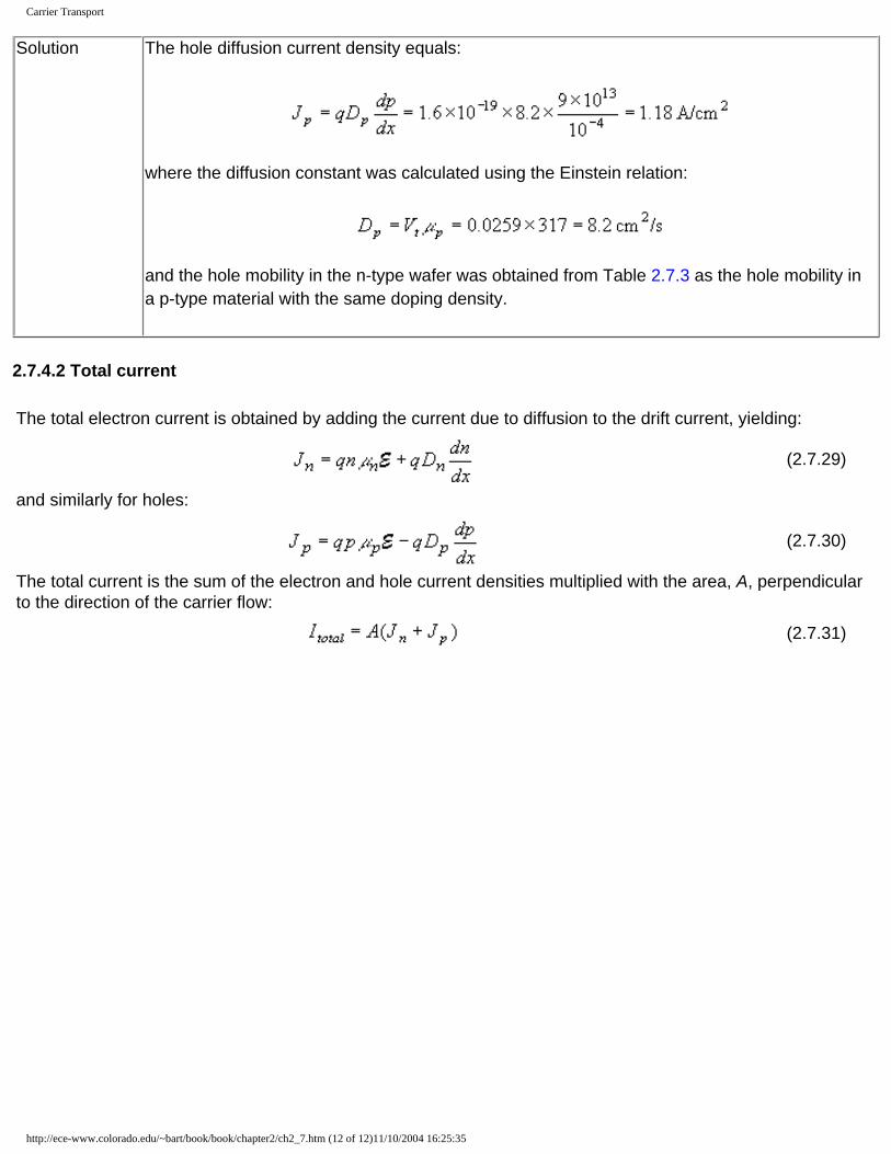
Carrier Transport
Solution The hole diffusion current density equals:
where the diffusion constant was calculated using the Einstein relation:
and the hole mobility in the n-type wafer was obtained from Table 2.7.3 as the hole mobility in a p-type material with the same doping density.
2.7.4.2 Total current
The total electron current is obtained by adding the current due to diffusion to the drift current, yielding:
(2.7.29)
and similarly for holes:
(2.7.30)
The total current is the sum of the electron and hole current densities multiplied with the area, A, perpendicular to the direction of the carrier flow:
(2.7.31)
http://ece-www.colorado.edu/~bart/book/book/chapter2/ch2_7.htm (12 of 12)11/10/2004 16:25:35

2.7.5. The Hall Effect
The Hall effect describes the behavior of the free carriers in a semiconductor when applying an electric as well as a magnetic field. The experimental setup shown in Figure 2.7.7, depicts a semiconductor bar with a rectangular cross section and length L. A voltage Vx is applied between the two contacts, resulting in a field along the x-direction. The magnetic field is applied in the z-direction.
a) b)
Figure 2.7.7 Hall setup and carrier motion for a) holes and b) electrons.
As shown in Figure 2.7.7 a), the holes move in the positive x-direction. The magnetic field causes a force to act on the mobile particles in a direction dictated by the right hand rule. As a result there is a force, Fy, along the positive y-direction, which moves the holes to the right. In steady state this force is balanced by an electric field, Ey, so that there is no net force on the holes. As a result there is a voltage across the sample, which can be measured with a high-impedance voltmeter. This voltage, VH, is called the Hall voltage. Given the sign convention as shown in Figure 2.7.7, the hall voltage is positive for holes.
The behavior of electrons is shown in Figure 2.7.7 b). The electrons travel in the negative x-direction. Therefore the force, Fy, is in the positive y-direction due to the negative charge and the electrons move to the right, just like holes. The balancing electric field, Ey, now has the opposite sign, which results in a negative Hall voltage.
To calculate the Hall field, we first calculate the Lorentz force acting on the free carriers:
)( BvqFrrrr
×+= E (2.7.33)
We now assume that the carriers can only flow along the x-direction and label their velocity vx. The Lorentz force then becomes:
zzyzxyxx
z
x
zyx
qBvqqB
vqqF e e )(e 00
00
eeerrr
rrrrr
EEEE +−+=+=
(2.7.34)
Since the carriers only flow along the x-direction, the net force must be zero along the y and z direction. As a result, the electric field is zero along the z direction and:
L
W
t
Vx
zy
x
vxEx
Bz
Ey
<
Fyvx
Ey
Fy
-
++
-
VH- +
L
W
t
VxEx
Bz
-
+
VH+ -
IxIx
L
W
t
Vx
zy
x
vxEx
Bz
Ey
<
Fyvx
Ey
Fy
-
++
-
VH- +
L
W
t
VxEx
Bz
-
+
VH+ -
IxIx

0)( =−= zxyy BvqF E (2.7.35)
which provides a relation between the electric field along the y-direction and the applied magnetic field, which can also be rewritten as a function of the current density, Jx, using (2.7.8):
z
p
xzxy B
qpJ
Bv0
==E (2.7.36)
This electric field is called the Hall field. The Hall coefficient, RH, is defined as the Hall field divided by the applied current density and magnetic field:
0
1
pzx
yH qpBJ
==∆ E
R (2.7.37)
Once the Hall coefficient is obtained one easily finds the hole density:
y
zx
Hp q
BJq
pER
==1
0 (2.7.38)
The carrier mobility can also be extracted from the Hall coefficient:
ρ
µ H
xp
xp qp
J RE
==0
(2.7.39)
Where ρ is the resistivity of the semiconductor.
The Hall coefficient can be calculated from the measured current, Ix, and measured voltage, VH:
WtL
BIV
zx
HH =R
(2.7.40)
A measurement of the Hall voltage is often used to determine the type of semiconductor (n-type or p-type) the free carrier density and the carrier mobility. Repeating the measurement at different temperatures allows one to measure the free carrier density as well as the mobility as a function of temperature. Since the measurement can be done on a small piece of uniformly doped material it is by far the easiest measurement to determine the carrier mobility. It should be noted that the scattering mechanisms in the presence of a magnetic field are different and that the measured Hall mobility can differ somewhat from the drift mobility. A measurement of the carrier density versus temperature provides information regarding the ionization energies of the donors and acceptor that are present in the semiconductor as described in section 2.6.4.4. While the interpretation of the Hall measurement is straightforward in the case of a single dopant, multiple types of impurities and the presence of electrons and holes can make the interpretation non-trivial.

Carrier recombination and generation
Title Page Table of Contents Help Copyright B. Van Zeghbroeck, 2004
Chapter 2: Semiconductor Fundamentals
2.8. Carrier recombination and generation2.8.1. Simple recombination-generation model2.8.2. Band-to-band recombination2.8.3. Trap assisted recombination2.8.4. Surface recombination2.8.5. Auger recombination2.8.6. Generation due to light 2.8.7. Derivation of trap-assisted recombination
Recombination of electrons and holes is a process by which both carriers annihilate each other: electrons occupy - through one or multiple steps - the empty state associated with a hole. Both carriers eventually disappear in the process. The energy difference between the initial and final state of the electron is released in the process. This leads to one possible classification of the recombination processes. In the case of radiative recombination, this energy is emitted in the form of a photon. In the case of non-radiative recombination, it is passed on to one or more phonons and in Auger recombination it is given off in the form of kinetic energy to another electron. Another classification scheme considers the individual energy levels and particles involved. These different processes are further illustrated with Figure 2.8.1.
Figure 2.8.1 : Carrier recombination mechanisms in semiconductorsBand-to-band recombination occurs when an electron falls from its conduction band state into the empty valence band state associated with the hole. This band-to-band transition is typically also a radiative transition in direct bandgap semiconductors.
http://ece-www.colorado.edu/~bart/book/book/chapter2/ch2_8.htm (1 of 6)11/10/2004 16:26:05
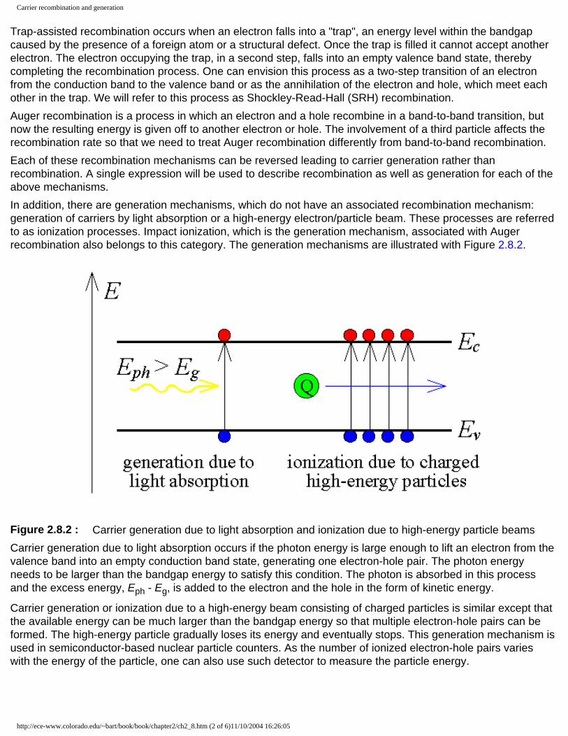
Carrier recombination and generation
Trap-assisted recombination occurs when an electron falls into a "trap", an energy level within the bandgap caused by the presence of a foreign atom or a structural defect. Once the trap is filled it cannot accept another electron. The electron occupying the trap, in a second step, falls into an empty valence band state, thereby completing the recombination process. One can envision this process as a two-step transition of an electron from the conduction band to the valence band or as the annihilation of the electron and hole, which meet each other in the trap. We will refer to this process as Shockley-Read-Hall (SRH) recombination. Auger recombination is a process in which an electron and a hole recombine in a band-to-band transition, but now the resulting energy is given off to another electron or hole. The involvement of a third particle affects the recombination rate so that we need to treat Auger recombination differently from band-to-band recombination. Each of these recombination mechanisms can be reversed leading to carrier generation rather than recombination. A single expression will be used to describe recombination as well as generation for each of the above mechanisms. In addition, there are generation mechanisms, which do not have an associated recombination mechanism: generation of carriers by light absorption or a high-energy electron/particle beam. These processes are referred to as ionization processes. Impact ionization, which is the generation mechanism, associated with Auger recombination also belongs to this category. The generation mechanisms are illustrated with Figure 2.8.2.
Figure 2.8.2 : Carrier generation due to light absorption and ionization due to high-energy particle beamsCarrier generation due to light absorption occurs if the photon energy is large enough to lift an electron from the valence band into an empty conduction band state, generating one electron-hole pair. The photon energy needs to be larger than the bandgap energy to satisfy this condition. The photon is absorbed in this process and the excess energy, Eph - Eg, is added to the electron and the hole in the form of kinetic energy.
Carrier generation or ionization due to a high-energy beam consisting of charged particles is similar except that the available energy can be much larger than the bandgap energy so that multiple electron-hole pairs can be formed. The high-energy particle gradually loses its energy and eventually stops. This generation mechanism is used in semiconductor-based nuclear particle counters. As the number of ionized electron-hole pairs varies with the energy of the particle, one can also use such detector to measure the particle energy.
http://ece-www.colorado.edu/~bart/book/book/chapter2/ch2_8.htm (2 of 6)11/10/2004 16:26:05

Carrier recombination and generation
Finally, there is a generation process called impact ionization, the generation mechanism that is the counterpart of Auger recombination. Impact ionization is caused by an electron/hole with an energy, which is much larger/smaller than the conduction/valence band edge. The detailed mechanism is illustrated with Figure 2.8.3.
Figure 2.8.3: Impact ionization and avalanche multiplication of electrons and holes in the presence of a large electric field.
The excess energy is given off to generate an electron-hole pair through a band-to-band transition. This generation process causes avalanche multiplication in semiconductor diodes under high reverse bias: As one carrier accelerates in the electric field it gains energy. The kinetic energy is given off to an electron in the valence band, thereby creating an electron-hole pair. The resulting two electrons can create two more electrons which generate four more causing an avalanche multiplication effect. Electrons as well as holes contribute to avalanche multiplication.
2.8.1. Simple recombination-generation model
A simple model for the recombination-generation mechanisms states that the recombination-generation rate is proportional to the excess carrier density. It acknowledges the fact that no recombination takes place if the carrier density equals the thermal equilibrium value. The resulting expression for the recombination of electrons in a p-type semiconductor is given by:
http://ece-www.colorado.edu/~bart/book/book/chapter2/ch2_8.htm (3 of 6)11/10/2004 16:26:05

Carrier recombination and generation
(2.8.1)
and similarly for holes in an n-type semiconductor:
(2.8.2)
where the parameter τ can be interpreted as the average time after which an excess minority carrier recombines. We will show for each of the different recombination mechanisms that the recombination rate can be simplified to this form when applied to minority carriers in a "quasi-neutral" semiconductor. The above expressions are therefore only valid under these conditions. The recombination rates of the majority carriers equals that of the minority carriers since in steady state recombination involves an equal number of holes and electrons. Therefore, the recombination rate of the majority carriers depends on the excess-minority-carrier-density as the minority carriers limit the recombination rate. Recombination in a depletion region and in situations where the hole and electron density are close to each other cannot be described with the simple model and the more elaborate expressions for the individual recombination mechanisms must be used.
2.8.2. Band-to-band recombination
Band-to-band recombination depends on the density of available electrons and holes. Both carrier types need to be available in the recombination process. Therefore, the rate is expected to be proportional to the product of n and p. Also, in thermal equilibrium, the recombination rate must equal the generation rate since there is no net recombination or generation. As the product of n and p equals ni2 in thermal equilibrium, the net recombination rate can be expressed as:
(2.8.3)
where b is the bimolecular recombination constant.
2.8.3. Trap assisted recombination
The net recombination rate for trap-assisted recombination is given by:
(2.8.4)
This expression can be further simplified for p >> n to:
(2.8.5)
and for n >> p to:
http://ece-www.colorado.edu/~bart/book/book/chapter2/ch2_8.htm (4 of 6)11/10/2004 16:26:05

Carrier recombination and generation
(2.8.6)
were
(2.8.7)
2.8.4. Surface recombination
Recombination at semiconductor surfaces and interfaces can have a significant impact on the behavior of devices. This is because surfaces and interfaces typically contain a large number of recombination centers because of the abrupt termination of the semiconductor crystal, which leaves a large number of electrically active dangling bonds. In addition, the surfaces and interfaces are more likely to contain impurities since they are exposed during the device fabrication process. The net recombination rate due to trap-assisted recombination and generation is given by:
(2.8.8)
This expression is almost identical to that of Shockley-Hall-Read recombination. The only difference is that the recombination is due to a two-dimensional density of traps, Nts, as the traps only exist at the surface or interface.This equation can be further simplified for minority carriers in a quasi-neutral region. For instance for electrons in a quasi-neutral p-type region p >> n and p >> ni so that for Ei = Est, it can be simplified to:
(2.8.9)
where the recombination velocity, vs, is given by:
(2.8.10)
2.8.5. Auger recombination
Auger recombination involves three particles: an electron and a hole, which recombine in a band-to-band transition and give off the resulting energy to another electron or hole. The expression for the net recombination rate is therefore similar to that of band-to-band recombination but includes the density of the electrons or holes, which receive the released energy from the electron-hole annihilation:
(2.8.11)
The two terms correspond to the two possible mechanisms.
2.8.6. Generation due to light
http://ece-www.colorado.edu/~bart/book/book/chapter2/ch2_8.htm (5 of 6)11/10/2004 16:26:05

Carrier recombination and generation
Carriers can be generated in semiconductors by illuminating the semiconductor with light. The energy of the incoming photons is used to bring an electron from a lower energy level to a higher energy level. In the case where an electron is removed from the valence band and added to the conduction band, an electron-hole pair is generated. A necessary condition for this to happen is that the energy of the photon, Eph, is larger than the bandgap energy, Eg. As the energy of the photon is given off to the electron, the photon no longer exists.
If each absorbed photon creates one electron-hole pair, the electron and hole generation rates are given by:
(2.8.12)
where α is the absorption coefficient of the material at the energy of the incoming photon. The absorption of light in a semiconductor causes the optical power to decrease with distance. This effect is described mathematically by:
(2.8.13)
The calculation of the generation rate of carriers therefore requires first a calculation of the optical power within the structure from which the generation rate can then be obtained using (2.8.12).
Example 2.11 Calculate the electron and hole densities in an n-type silicon wafer (Nd = 1017 cm-3) illuminated uniformly with 10 mW/cm2 of red light (Eph = 1.8 eV). The absorption coefficient of red light in silicon is 10-3 cm-1. The minority carrier lifetime is 10 µs.
Solution The generation rate of electrons and holes equals:
where the photon energy was converted into Joules. The excess carrier densities are then obtained from:
The excess carrier densities are then obtained from: So that the electron and hole densities equal:
http://ece-www.colorado.edu/~bart/book/book/chapter2/ch2_8.htm (6 of 6)11/10/2004 16:26:05

Continuity equation
Title Page Table of Contents Help Copyright B. Van Zeghbroeck, 2004
Chapter 2: Semiconductor Fundamentals
2.9. Continuity equation2.9.1. Derivation2.9.2. The diffusion equation2.9.3. Steady state solution to the diffusion equation
2.9.1. Derivation
The continuity equation describes a basic concept, namely that a change in carrier density over time is due to the difference between the incoming and outgoing flux of carriers plus the generation and minus the recombination. The flow of carriers and recombination and generation rates are illustrated with Figure 2.9.1.
Figure 2.9.1 : Electron currents and possible recombination and generation processesThe rate of change of the carriers between x and x + dx equals the difference between the incoming flux and the outgoing flux plus the generation and minus the recombination:
(2.9.1)
where n(x,t) is the carrier density, A is the area, Gn(x,t) is the generation rate and Rn(x,t) is the recombination rate. Using a Taylor series expansion,
(2.9.2)
http://ece-www.colorado.edu/~bart/book/book/chapter2/ch2_9.htm (1 of 3)11/10/2004 16:26:38

Continuity equation
this equation can be formulated as a function of the derivative of the current:
(2.9.3)
and similarly for holes one finds:
(2.9.4)
A solution to these equations can be obtained by substituting the expression for the electron and hole current, (2.7.29) and (2.7.30). This then yields two partial differential equations as a function of the electron density, the hole density and the electric field. The electric field itself is obtained from Gauss's law.
(2.9.5)
(2.9.6)
A generalization in three dimensions yields the following continuity equations for electrons and holes:
(2.9.7)
(2.9.8)
2.9.2. The diffusion equation
In the quasi-neutral region - a region containing mobile carriers, where the electric field is small - the current is due to diffusion only. In addition, we can use the simple recombination model for the net recombination rate. This leads to the time-dependent diffusion equations for electrons in p-type material and for holes in n-type material:
(2.9.9)
(2.9.10)
http://ece-www.colorado.edu/~bart/book/book/chapter2/ch2_9.htm (2 of 3)11/10/2004 16:26:38

Continuity equation
2.9.3. Steady state solution to the diffusion equation
In steady state, the partial derivatives with respect to time are zero, yielding:
(2.9.11)
(2.9.12)
The general solution to these second order differential equations are:
(2.9.13)
(2.9.14)
where Ln and Lp are the diffusion lengths given by:
(2.9.15)
(2.9.16)
The diffusion constants, Dn and Dp, are obtained using the Einstein relations (2.7.27) and (2.7.28). The diffusion equations can also be written as a function of the excess carrier densities, δn and δp, which are related to the total carrier densities, n and p, and the thermal equilibrium densities, n0 and p0, by:
(2.9.17)
(2.9.18)
yielding:
(2.9.19)
(2.9.20)
The diffusion equation will be used to calculate the diffusion current in p-n junctions and bipolar transistors.
http://ece-www.colorado.edu/~bart/book/book/chapter2/ch2_9.htm (3 of 3)11/10/2004 16:26:38

The drift-diffusion model
Title Page Table of Contents Help Copyright B. Van Zeghbroeck, 2004
Chapter 2: Semiconductor Fundamentals
2.10. The drift-diffusion model
The drift-diffusion model of a semiconductor is frequently used to describe semiconductor devices. It contains all the features described in this chapter. Starting with Chapter 3, we will apply the drift-diffusion model to a variety of different devices. To facilitate this analysis, we present here a simplified drift-diffusion model, which contains all the essential features. This model results in a set of ten variables and ten equations.The assumptions of the simplified drift-diffusion model are:
Full ionization: all dopants are assumed to be ionized (shallow dopants)Non-degenerate: the Fermi energy is assumed to be at least 3 kT below/above the conduction/valence band edge.Steady state: All variables are independent of timeConstant temperature: The temperature is constant throughout the device.
The ten variables are the following:
ρ, the charge densityn, the electron densityp, the hole density
, the electric field
φ, the potentialEi, the intrinsic energy
Fn, the electron quasi-Fermi energy
Fp, the hole quasi-Fermi energy
Jn, the electron current density
Jp, the hole current density
The ten equations are:Charge density equation
(2.10.1)
Electric field and potential equations
http://ece-www.colorado.edu/~bart/book/book/chapter2/ch2_10.htm (1 of 2)11/10/2004 16:26:50

The drift-diffusion model
(2.10.2)
(2.10.3)
(2.10.4)
Carrier density equations
(2.10.5)
(2.10.6)
Drift and diffusion current equations
(2.10.7)
(2.10.8)
Continuity equation in steady state with SHR recombination
(2.10.9)
(2.10.10)
http://ece-www.colorado.edu/~bart/book/book/chapter2/ch2_10.htm (2 of 2)11/10/2004 16:26:50

2.11. Semiconductor thermodynamics Thermodynamics can be used to explain some characteristics of semiconductors and semiconductor devices, which at times seem inexplicable. One example is the fact that the Fermi energy is located within the energy gap where there are no energy levels and therefore also no electrons or holes. This is because the Fermi energy describes the energy of the particles in the distribution. Thermodynamics can also be used to gain a completely different perspective. This section is therefore a worthwhile one to study as one can gain further insight into the field of semiconductors. However, it is not required to understand the following chapters.
2.11.1. Thermal equilibrium
A system is in thermal equilibrium if detailed balance is obtained. Detailed balance implies that every process in the system is exactly balanced by its inverse process. As a result, there is no net effect on the system.
This definition implies that in thermal equilibrium no energy (heat, work or particle energy) is exchanged between the parts within the system and between the system and the environment. Thermal equilibrium is obtained by isolating a system from its environment, removing any internal sources of energy, and waiting for a long enough time until the system does not change any more.
The concept of thermal equilibrium is of interest since a variety of thermodynamic results assume that the system under consideration is in thermal equilibrium. Few systems of interest rigorously satisfy this condition so that we often apply the thermodynamical results to systems, which are "close" to thermal equilibrium. Agreement between theories based on this assumption and experiments justify this approach.
2.11.2. Thermodynamic identity
The thermodynamic identity simply states that adding heat, work or particles can cause a change in energy. Mathematically this is expressed by:
dNdWdQdU µ++= (2.11.1)
where U is the energy, Q is the heat and W is the work. µ is the energy added to a system when adding one particle without adding either heat or work. The amount of heat exchanged depends on the temperature, T, and the entropy, S, while the amount of work delivered to a system depends on the pressure, p, and the volume, V, or:
TdSdQ = (2.11.2)
and
pdVdW −= (2.11.3)
yielding:
dNpdVTdSdU µ+−= (2.11.4)

2.11.3. The Fermi energy
The Fermi energy, EF, is the energy associated with a particle, which is in thermal equilibrium with the system of interest. The energy is strictly associated with the particle and does not consist even in part of heat or work. This same quantity is called the electro-chemical potential, µ, in most thermodynamics texts.
2.11.4. Example: an ideal electron gas
As an example to illustrate the difference between the average energy of particles in a system and the Fermi energy we now consider an ideal electron gas. The term ideal refers to the fact that the gas obeys the ideal gas law. To be "ideal" the gas must consist of particles, which do not interact with each other.
The total energy of the non-degenerate electron gas containing N particles equals:
cNENkTU +=
23
(2.11.5)
as each non-relativistic electron has a thermal energy of kT/2 for each degree of freedom in addition to its minimum energy, Ec. The product of the pressure and volume is given by the ideal gas law:
NkTpV = (2.11.6)
While the Fermi energy is given by:
ccF N
nkTEE ln+=
(2.11.7)
The thermodynamic identity can now be used to find the entropy from:
T
pVNUS
+−=
µ
(2.11.8)
yielding:
cNn
NkNkS ln25
−= (2.11.9)
This relation can be visualized on an energy band diagram when one considers the energy, work and entropy per electron and compares it to the electro-chemical potential as shown in figure 1.
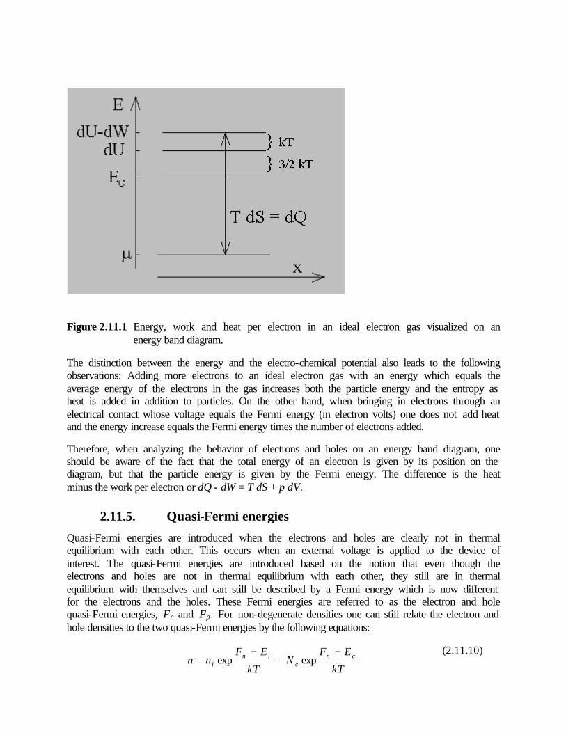
Figure 2.11.1 Energy, work and heat per electron in an ideal electron gas visualized on an energy band diagram.
The distinction between the energy and the electro-chemical potential also leads to the following observations: Adding more electrons to an ideal electron gas with an energy which equals the average energy of the electrons in the gas increases both the particle energy and the entropy as heat is added in addition to particles. On the other hand, when bringing in electrons through an electrical contact whose voltage equals the Fermi energy (in electron volts) one does not add heat and the energy increase equals the Fermi energy times the number of electrons added.
Therefore, when analyzing the behavior of electrons and holes on an energy band diagram, one should be aware of the fact that the total energy of an electron is given by its position on the diagram, but that the particle energy is given by the Fermi energy. The difference is the heat minus the work per electron or dQ - dW = T dS + p dV.
2.11.5. Quasi-Fermi energies
Quasi-Fermi energies are introduced when the electrons and holes are clearly not in thermal equilibrium with each other. This occurs when an external voltage is applied to the device of interest. The quasi-Fermi energies are introduced based on the notion that even though the electrons and holes are not in thermal equilibrium with each other, they still are in thermal equilibrium with themselves and can still be described by a Fermi energy which is now different for the electrons and the holes. These Fermi energies are referred to as the electron and hole quasi-Fermi energies, Fn and Fp. For non-degenerate densities one can still relate the electron and hole densities to the two quasi-Fermi energies by the following equations:
kT
EFN
kT
EFnn cn
cin
i
−=
−= expexp
(2.11.10)

kTFE
NkT
FEnp nv
vpi
i
−=
−= expexp
(2.11.11)
2.11.6. Energy loss in recombination processes
The energy loss in a recombination process equals the difference between the electron and hole quasi-Fermi energies as the energy loss is only due to the energy of the particles, which are lost:
pn FFU −=∆ (2.11.12)
No heat or work is removed from the system, just the energy associated with the particles. The energy lost in the recombination process can be converted in heat or light depending on the details of the process.
2.11.7. Thermo-electric effects in semiconductors
The temperature dependence of the current in a semiconductor can be included by generalizing the drift-diffusion equation for the current. The proportionality constant between the current density and the temperature gradient is the product of the conductivity and the thermo-electric power.
The derivation starts by generalizing the diffusion current to include a possible variation of the diffusion constant with position, yielding:
dxnDd
qnqJ nnn
)(+= Eµ
(2.11.13)
If the semiconductor is non-degenerate the electron density can be related to the effective density of states and the difference between the Fermi energy and the conduction band edge:
kTEE
Nn cFc
−= exp
(2.11.14)
yielding:
−
++++=dxkT
EEd
kTdx
dNNkT
dxdkT
dxdT
kdx
dEnJ
cF
c
c
n
n
cnn
)(µ
µµ
(2.11.15)
For the case where the material properties do not change with position, all the spatial variations except for the gradient of the Fermi energy are caused by a temperature variation. We postulate that the current can be written in the following form:

−=
dxdT
qdx
dEnJ c
nn Pµ (2.11.16)
and P is the thermo-electric power in Volt/Kelvin. From both equations one then obtains the thermo-electric power:
++−=
nN
dxdT
kq cn
nn ln
25 µ
µP
(2.11.17)
If the temperature dependence of the mobility can be expressed as a simple power law:
sn T −∝µ (2.11.18)
the thermo-electric power becomes:
+−−=
nN
skq cn ln
25P
(2.11.19)
for n-type material and similarly for p-type material:
+−=
pN
skq vp ln
25
P (2.11.20)
The Peltier coefficient, Π, is related to the thermo-electric power by:
TP=Π (2.11.21)
If electrons and holes are present in the semiconductor one has to include the effect of both when calculating the Peltier coefficient by
pn
ppnntotal σσ
σσ
+
Π+Π=Π
(2.11.22)
The resulting Peltier coefficient as a function of temperature for silicon is shown in the figure below:
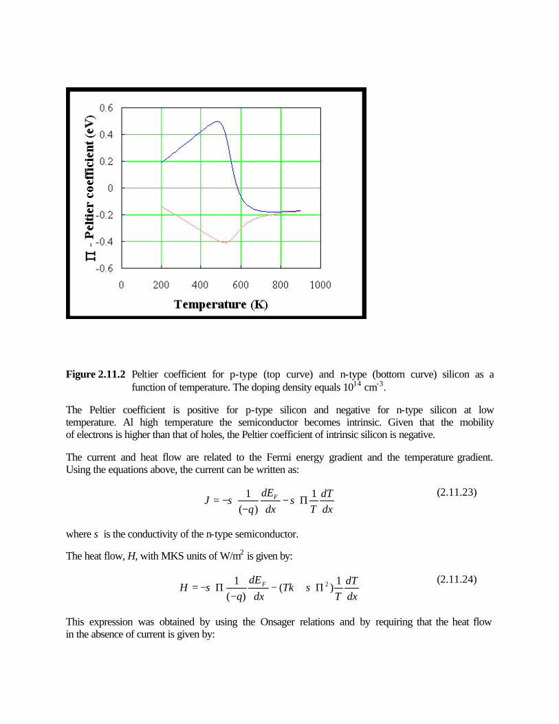
Figure 2.11.2 Peltier coefficient for p-type (top curve) and n-type (bottom curve) silicon as a function of temperature. The doping density equals 1014 cm-3.
The Peltier coefficient is positive for p-type silicon and negative for n-type silicon at low temperature. Al high temperature the semiconductor becomes intrinsic. Given that the mobility of electrons is higher than that of holes, the Peltier coefficient of intrinsic silicon is negative.
The current and heat flow are related to the Fermi energy gradient and the temperature gradient. Using the equations above, the current can be written as:
dxdT
TdxdE
qJ F 1
)(1
Π−−
−= σσ (2.11.23)
where σ is the conductivity of the n-type semiconductor.
The heat flow, H, with MKS units of W/m2 is given by:
dxdT
TT
dxdE
qH F 1
)()(
1 2Π+−−
Π−= σκσ (2.11.24)
This expression was obtained by using the Onsager relations and by requiring that the heat flow in the absence of current is given by:
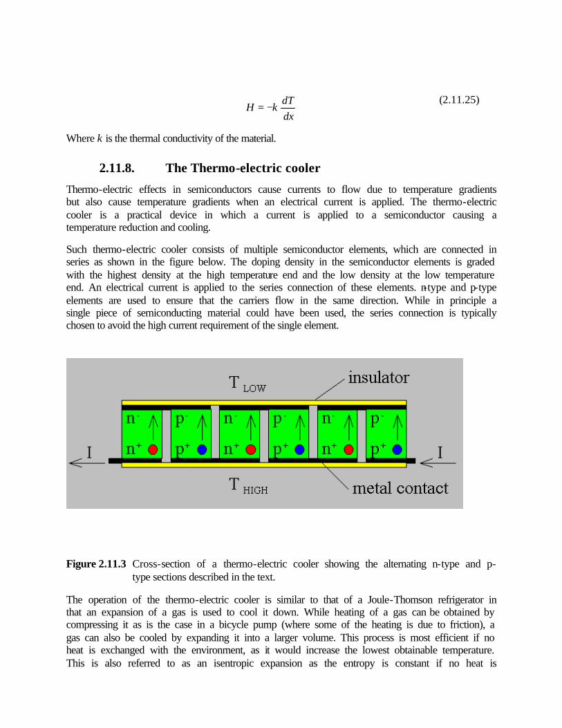
dxdT
H κ−= (2.11.25)
Where κ is the thermal conductivity of the material.
2.11.8. The Thermo-electric cooler
Thermo-electric effects in semiconductors cause currents to flow due to temperature gradients but also cause temperature gradients when an electrical current is applied. The thermo-electric cooler is a practical device in which a current is applied to a semiconductor causing a temperature reduction and cooling.
Such thermo-electric cooler consists of multiple semiconductor elements, which are connected in series as shown in the figure below. The doping density in the semiconductor elements is graded with the highest density at the high temperature end and the low density at the low temperature end. An electrical current is applied to the series connection of these elements. n-type and p-type elements are used to ensure that the carriers flow in the same direction. While in principle a single piece of semiconducting material could have been used, the series connection is typically chosen to avoid the high current requirement of the single element.
Figure 2.11.3 Cross-section of a thermo-electric cooler showing the alternating n-type and p-type sections described in the text.
The operation of the thermo-electric cooler is similar to that of a Joule-Thomson refrigerator in that an expansion of a gas is used to cool it down. While heating of a gas can be obtained by compressing it as is the case in a bicycle pump (where some of the heating is due to friction), a gas can also be cooled by expanding it into a larger volume. This process is most efficient if no heat is exchanged with the environment, as it would increase the lowest obtainable temperature. This is also referred to as an isentropic expansion as the entropy is constant if no heat is

exchanged.
The gas in a thermo-electric cooler is the electron or hole gas. As a constant current is applied so that carriers flow from the high density to low-density region, one can imagine that the volume around a fixed number of carriers must increase as the carriers move towards the lower doped region. A possible energy band diagram is shown below:
Figure 2.11.4 Energy band diagram of an n-type element of the thermo electric cooler of Figure 2.11.3
At constant temperature and in thermal equilibrium there is no current as the diffusion current is balanced by the drift current associated with the built-in electric field caused by the graded doping density. As a current is applied to the semiconductor the built-in field is reduced so that the carriers diffuse from the high to low doping density. This causes a temperature reduction on the low-doped side, which continues until the entropy is constant throughout the semiconductor. Since the entropy per electron equals the distance between the conduction band edge and the Fermi energy plus 5/2 kT one finds that the conduction band edge is almost parallel to the Fermi energy.
An ideal isentropic expansion is not obtained due to the Joule heating caused by the applied current and the thermal losses due to the thermal conductivity of the material. The need to remove heat at the low temperature further increases the lowest achievable temperature.
2.11.9. The "hot-probe" experiment
The "hot-probe" experiment provides a very simple way to distinguish between n-type and p-type semiconductors using a soldering iron and a standard multi-meter.

The experiment is performed by contacting a semiconductor wafer with a "hot" probe such as a heated soldering iron and a "cold" probe. Both probes are wired to a sensitive current meter. The hot probe is connected to the positive terminal of the meter while the cold probe is connected to the negative terminal. The experimental set-up is shown in the figure below:
Figure 2.11.5 Experimental set-up of the "hot-probe" experiment.
When applying the probes to n-type material one obtains a positive current reading on the meter, while p-type material yields a negative current.
A simple explanation for this experiment is that the carriers move within the semiconductor from the hot probe to the cold probe. While diffusion seems to be a plausible mechanism to cause the carrier flow it is actually not the most important mechanism since the material is uniformly doped. However, as will be discussed below there is a substantial electric field in the semiconductor so that the drift current dominates the total current.
Starting from the assumption that the current meter has zero resistance, and ignoring the (small) thermoelectric effect in the metal wires one can justify that the Fermi energy does not vary throughout the material. A possible corresponding energy band diagram is shown below:

Figure 2.11.6 Energy band diagram corresponding to the "hot-probe" experiment illustrated by Figure 2.11.5.
This energy band diagram illustrates the specific case in which the temperature variation causes a linear change of the conduction band energy as measured relative to the Fermi energy, and also illustrates the trend in the general case. As the effective density of states decreases with decreasing temperature, one finds that the conduction band energy decreases with decreasing temperature yielding an electric field, which causes the electrons to flow from the high to the low temperature. The same reasoning reveals that holes in a p-type semiconductor will also flow from the higher to the lower temperature.
The current can be calculated from the general expression:
−=
dxdT
qdx
dEnJ c
nn Pµ (2.11.26)
where
++−=
nN
dxdT
kq cn
nn ln
25 µ
µP
(2.11.27)
The current will therefore increase with doping and with the applied temperature gradient as long as the semiconductor does not become degenerate or intrinsic within the applied temperature range.

example 3
Title Page Table of Contents Help Copyright B. Van Zeghbroeck, 2004
Chapter 2: Semiconductor Fundamentals
Examples
Example 2.1 Calculate the maximum fraction of the volume in a simple cubic crystal occupied by the atoms. Assume that the atoms are closely packed and that they can be treated as hard spheres. This fraction is also called the packing density.
Example 2.2 Calculate the energy bandgap of germanium, silicon and gallium arsenide at 300, 400, 500 and 600 K.
Example 2.3 Calculate the number of states per unit energy in a 100 by 100 by 10 nm piece of silicon (m* = 1.08 m0) 100 meV above the conduction band edge. Write the result in units of eV-1.
Example 2.4 Calculate the effective densities of states in the conduction and valence bands of germanium, silicon and gallium arsenide at 300 K.
Example 2.4b Calculate the intrinsic carrier density in germanium, silicon and gallium arsenide at 300, 400, 500 and 600 K.
Example 2.5 Calculate the ionization energy for shallow donors and acceptors in germanium and silicon using the hydrogen-like model.
Example 2.6a A germanium wafer is doped with a shallow donor density of 3ni/2. Calculate the electron and hole density.
Example 2.6b A silicon wafer is doped with a shallow acceptor doping of 1016 cm-3. Calculate the electron and hole density.
Example 2.6c 4H-SiC is doped with 2 x 1017 cm-3 nitrogen donor atoms (Ec – Ed = 90 meV). Use Nc = 4 x 1020 cm-3.
a. Calculate the electron density at 300 K. b. Calculate the hole density at 300 K after adding 2 x 1018 cm-3 aluminum acceptor
atoms (Ea – Ec = 220 meV) Use Nv = 1.6 x 1020 cm-3.
Example 2.7 A piece of germanium doped with 1016 cm-3 shallow donors is illuminated with light generating 1015 cm-3 excess electrons and holes. Calculate the quasi-Fermi energies relative to the intrinsic energy and compare it to the Fermi energy in the absence of illumination.
Example 2.8 Electrons in undoped gallium arsenide have a mobility of 8,800 cm2/V-s. Calculate the average time between collisions. Calculate the distance traveled between two collisions (also called the mean free path). Use an average velocity of 107 cm/s.
Example 2.9 A piece of silicon doped with arsenic (Nd = 1017 cm-3) is 100 µm long, 10 µm wide and 1 µm thick. Calculate the resistance of this sample when contacted one each end.
Example 2.10 The hole density in an n-type silicon wafer (Nd = 1017 cm-3) decreases linearly from 1014 cm-3 to 1013 cm-3 between x = 0 and x = 1 µm. Calculate the hole diffusion current density.
http://ece-www.colorado.edu/~bart/book/book/chapter2/ch2_ex.htm (1 of 2)11/10/2004 16:27:23

example 3
Example 2.11 Calculate the electron and hole densities in an n-type silicon wafer (Nd = 1017 cm-3) illuminated uniformly with 10 mW/cm2 of red light (Eph = 1.8 eV). The absorption coefficient of red light in silicon is 10-3 cm-1. The minority carrier lifetime is 10 µs.
http://ece-www.colorado.edu/~bart/book/book/chapter2/ch2_ex.htm (2 of 2)11/10/2004 16:27:23

Example 2.1 Calculate the maximum fraction of the volume in a simple cubic crystal occupied by the atoms. Assume that the atoms are closely packed and that they can be treated as hard spheres. This fraction is also called the packing density.
Solution The atoms in a simple cubic crystal are located at the corners of the units cell, a cube with side a. Adjacent atoms touch each other so that the radius of each atom equals a/2. There are eight atoms occupying the corners of the cube, but only one eighth of each is within the unit cell so that the number of atoms equals one per unit cell. The packing density is then obtained from:
% 52 6
)2
(34
34
cellunit theof Volumeatoms of Volume
3
3
3
3
====πππ
a
a
a
r
or about half the volume of the unit cell is occupied by the atoms. The packing density of four cubic crystals is listed in the table below. Radius Atoms/
unit cell Packing density
Simple cubic 2a
1
% 52 6
=π
Body centered cubic
43 a
2
% 68 8
3=
π
Face centered cubic
42 a
4
% 74 6
2=
π
Diamond
83 a
8
% 34 16
3=
π

Example 2.2 Calculate the energy bandgap of germanium, silicon and gallium arsenide at 300, 400, 500 and 600 K.
Solution The bandgap of silicon at 300 K equals:
eV 12.1636300
)300(10473.0166.1
)K 0()K 300(
23
2
=+
××−=
+−=
−
βαT
TEE gg
Similarly one finds the energy bandgap for germanium and gallium arsenide, as well as at different temperatures, yielding:
Germanium Silicon Gallium Arsenide
T = 300 K 0.66 eV 1.12 eV 1.42 eV T = 400 K 0.62 eV 1.09 eV 1.38 eV T = 500 K 0.58 eV 1.06 eV 1.33 eV
T = 600 K 0.54 eV 1.03 eV 1.28 eV

Example 2.3 Calculate the number of states per unit energy in a 100 by 100 by 10 nm piece of silicon (m* = 1.08 m0) 100 meV above the conduction band edge. Write the result in units of eV-1.
Solution The density of states equals:
1-3-56
19334
2/331
2/3*3
Jm 1051.1
106.11.0)10626.6(
)101.908.1(28
28)(
×=
×××
××=
−=
−−
−π
πcEEm
hEg
So that the total number of states per unit energy equals:
eV 1041.2J 101051.1)( -15-12256 ×=××= −VEg

Example 2.4 Calculate the effective densities of states in the conduction and valence bands of germanium, silicon and gallium arsenide at 300 K.
Solution The effective density of states in the conduction band of germanium equals:
3-193-25
2/3234
2331
2/32
*
cm 1002.1m 1002.1
))10626.6(
3001038.11011.955.02(2
)2
(2
×=×=
×
×××××=
=
−
−−π
π
h
kTmN e
c
where the effective mass for density of states was used (see appendix 3 or section 2.3.6). Similarly one finds the effective density of states in the conduction band for other semiconductors and the effective density of states in the valence band:
Germanium Silicon Gallium Arsenide
Nc (cm-3) 1.02 x 10¹⁹ 2.81 x 10¹⁹ 4.35 x 10¹⁷
Nv (cm-3) 5.64 x 10¹⁸ 1.83 x 10¹⁹ 7.57 x 10¹⁸ Note that the effective density of states is temperature dependent
and can be obtain from: 2/3)
300()K 300()(
TNTN cc =
where Nc(300 K) is the effective density of states at 300 K.
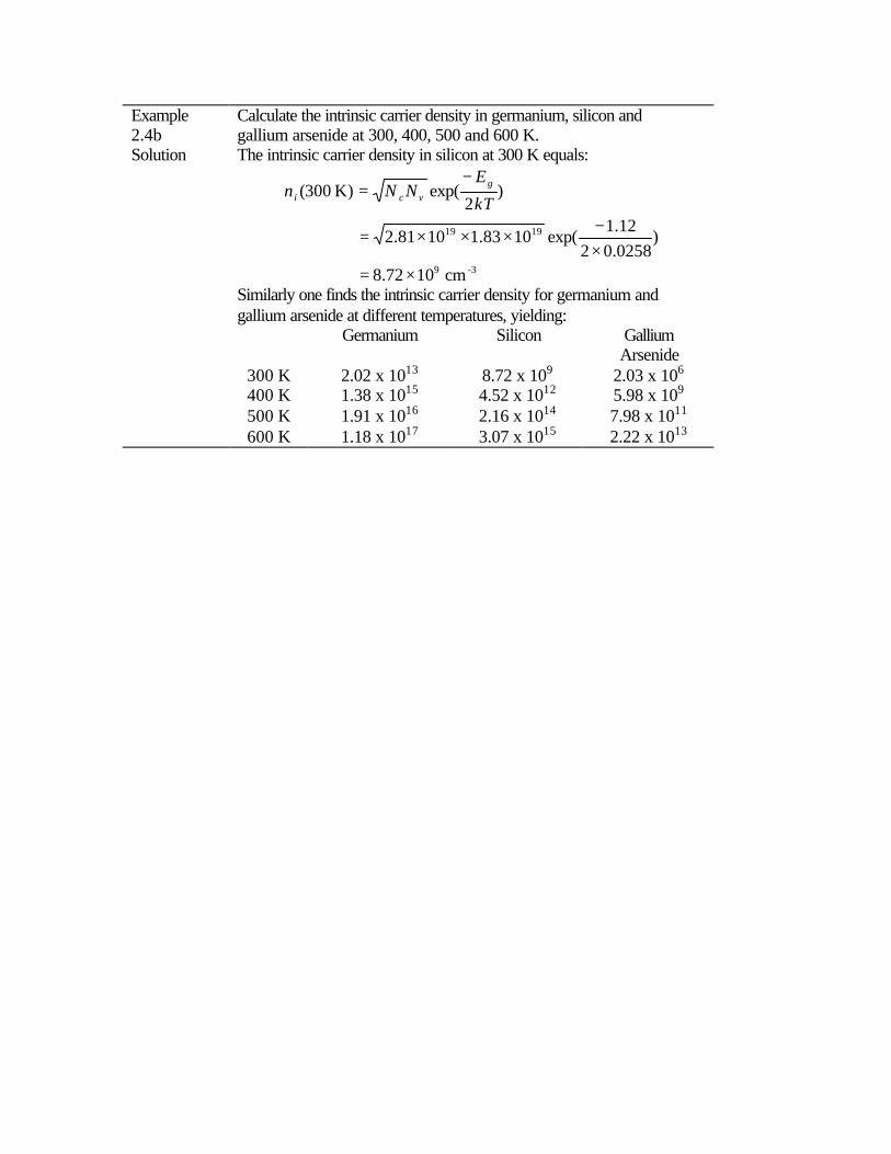
Example 2.4b
Calculate the intrinsic carrier density in germanium, silicon and gallium arsenide at 300, 400, 500 and 600 K.
Solution The intrinsic carrier density in silicon at 300 K equals:
3-9
1919
cm 1072.8
)0258.0212.1
exp(1083.11081.2
)2
exp()K 300(
×=×−
×××=
−=
kT
ENNn g
vci
Similarly one finds the intrinsic carrier density for germanium and gallium arsenide at different temperatures, yielding:
Germanium Silicon Gallium Arsenide
300 K 2.02 x 10¹³ 8.72 x 10⁹ 2.03 x 10⁶ 400 K 1.38 x 10¹⁵ 4.52 x 10¹² 5.98 x 10⁹ 500 K 1.91 x 10¹⁶ 2.16 x 10¹⁴ 7.98 x 10¹¹
600 K 1.18 x 10¹⁷ 3.07 x 10¹⁵ 2.22 x 10¹³

Example 2.5 Calculate the ionization energy for shallow donors and acceptors in germanium and silicon using the hydrogen-like model.
Solution Using the effective mass for conductivity calculations (Appendix 3) one finds the ionization energy for shallow donors in germanium to be:
meV 4.6eV 16
12.06.13eV 6.13
220
*===−
r
conddc
m
mEE
ε
The calculated ionization energies for donors and acceptors in germanium and silicon are provided below.
Germanium Silicon donors 6.4 meV 13.8 meV
acceptors 11.2 meV 20.5 meV Note that the actual ionization energies differ from this value and
depend on the actual donor atom.

Example 2.6a A germanium wafer is doped with a shallow donor density of 3ni/2. Calculate the electron and hole density.
Solution The electron density is obtained from equation (2.6.34)
ii
iadad
o
nn
nNNNN
n
2)1169
43
(
)2
(2
22
=++=
+−
+−
=−+−+
and the hole density is obtained using the mass action law:
2
2i
o
io
nnn
p ==
Example 2.6b A silicon wafer is doped with a shallow acceptor doping of 1016 cm-3. Calculate the electron and hole density.
Solution Since the acceptor doping is much larger than the intrinsic density and much smaller than the effective density of states, the hole density equals:
-316 cm 10 =≅ +ao Np
The electron density is then obtained using the mass action law
3-416
202cm 10
10
10 ==≅
+a
io
N
nn
The approach described in example 2.6a yields the same result.

Example 2.6c 4H-SiC is doped with 2 x 1017 cm-3 nitrogen donor atoms (Ec –
Ed = 90 meV). Use Nc = 4 x 1020 cm-3. a) Calculate the electron density at 300 K. b) Calculate the hole density at 300 K after adding 2 x 10¹⁸
cm-3 aluminum acceptor atoms (Ea – Ec = 220 meV) Use Nv = 1.6 x 1020 cm-3.
Solution a) First we calculate N*
kTEEN
N cdc −= exp
2* = 6.16 x 1017 cm-3
The free electron density is then obtained from:
do NNNN
n *2**
4)(
2++−= = 4.3 x 1016 cm-3
As a result 21.5 % of the donors are ionized
b) Since we are now dealing with p-type material we have to recalculate N*
kTEEN
N avv −= exp
4* = 8.08 x 1016 cm-3
where the factor 4 is due to the doubly degenerate valence band. The free hole density is then obtained from:
)(4
)(2
*2**
dadd
o NNNNNNN
p −++
++
−=
= 5.52 x 1016 cm-3 which is identical to (2.6.42) except that the donor and acceptor densities have been exchanged. Only 2.76 % of the acceptors are ionized while all donors are ionized.

Example 2.7 A piece of germanium doped with 1016 cm-3 shallow donors is illuminated with light generating 1015 cm-3 excess electrons and holes. Calculate the quasi-Fermi energies relative to the intrinsic energy and compare it to the Fermi energy in the absence of illumination.
Solution The carrier densities when illuminating the semiconductor are: -3161516 cm 101.11010 ×=+=+= nnn o δ
-315 cm 10≅+= ppp o δ and the quasi-Fermi energies are:
meV 163102
101.1ln0259.0ln
13
16=
×
××==−
iin n
nkTEF
meV 101102
101ln0259.0ln
13
15−=
×
××=−=−
iip n
pkTEF
In comparison, the Fermi energy in the absence of light equals
meV 161102
10ln0259.0ln
13
16=
××==−
i
oiF n
nkTEE
which is very close to the quasi-Fermi energy of the majority carriers.

Example 2.8 Electrons in undoped gallium arsenide have a mobility of 8,800 cm2/V-s. Calculate the average time between collisions. Calculate the distance traveled between two collisions (also called the mean free path). Use an average velocity of 107 cm/s.
Solution The collision time, τc, is obtained from:
ps 0.34 106.1
101.9067.088.019
31*=
×
×××==−
−
qmen
cµ
τ
where the mobility was first converted to MKS units. The mean free path, l, equals:
nm 341034.010 127 =××== −caveragevl τ

Example 2.9 A piece of silicon doped with arsenic (Nd = 1017 cm-3) is 100 µm long, 10 µm wide and 1 µm thick. Calculate the resistance of this sample when contacted one each end.
Solution The resistivity of the silicon equals:
cm 086.072710106.1
111719
Ω=×××
==−
nqnµρ
where the mobility was obtained from Table 2.7.3. The resistance then equals:
Ω=××
××== −−
−
k 6.8101010
10100086.0 44
4
WtL
R ρ
An alternate approach is to first calculate the sheet resistance, Rs:
square/ 86010
086.04 Ω=== −t
Rsρ
From which one then obtains the resistance:
Ω=×
××== −
−
k 6.81010
10100860 4
4
WL
RR s
Example 2.10 The hole density in an n-type silicon wafer (Nd = 1017 cm-3) decreases linearly from 1014 cm-3 to 1013 cm-3 between x = 0 and x = 1 µm. Calculate the hole diffusion current density.
Solution The hole diffusion current density equals:
24
1319 A/cm 18.1
10
1092.8106.1 =
××××== −
−
dxdp
qDJ pp
where the diffusion constant was calculated using the Einstein relation:
/scm 2.83170259.0 2=×== ptp VD µ and the hole mobility in the n-type wafer was obtained from Table 2.7.3 as the hole mobility in a p-type material with the same doping density.

Example 2.11 Calculate the electron and hole densities in an n-type silicon wafer (Nd = 1017 cm-3) illuminated uniformly with 10 mW/cm2 of red light (Eph = 1.8 eV). The absorption coefficient of red light in silicon is 10-3 cm-1. The minority carrier lifetime is 10 µs.
Solution The generation rate of electrons and holes equals:
1-3-1319
23 scm 105.3
106.18.110
10 ×=××
===−
−−
AE
PGG
ph
optpn α
where the photon energy was converted into Joules. The excess carrier densities are then obtained from:
-38136 cm 105.3105.31010 ×=×××=== −ppGpn τδδ
So that the electron and hole densities equal: -317817 cm 10105.310 =×+=+= nnn o δ
3-8817
2102
cm 105.3105.310
)10(×=×+=+= p
nn
po
i δ

http://ece-www.colorado.edu/~bart/book/book/chapter2/ch2_p.htm
Title Page Table of Contents Help Copyright B. Van Zeghbroeck, 2004
Chapter 2: Semiconductor Fundamentals
Problems
1. Calculate the packing density of the body centered cubic, the face centered cubic and the diamond lattice, listed in example 2.1.
2. At what temperature does the energy bandgap of silicon equal exactly 1 eV?
3. Prove that the probability of occupying an energy level below the Fermi energy equals the probability that an energy level above the Fermi energy and equally far away from the Fermi energy is not occupied.
4. At what energy (in units of kT) is the Fermi function within 1 % of the Maxwell-Boltzmann distribution function? What is the corresponding probability of occupancy?
5. Calculate the Fermi function at 6.5 eV if EF = 6.25 eV and T = 300 K. Repeat at T = 950 K assuming that the Fermi energy does not change. At what temperature does the probability that an energy level at E = 5.95 eV is empty equal 1 %.
6. Calculate the effective density of states for electrons and holes in germanium, silicon and gallium arsenide at room temperature and at 100 °C. Use the effective masses for density of states calculations.
7. Calculate the intrinsic carrier density in germanium, silicon and gallium arsenide at room temperature (300 K). Repeat at 100 °C. Assume that the energy bandgap is independent of temperature and use the room temperature values.
8. Calculate the position of the intrinsic energy level relative to the midgap energy
Emidgap = (Ec + Ev)/2
in germanium, silicon and gallium arsenide at 300 K. Repeat at T = 100 °C.
9. Calculate the electron and hole density in germanium, silicon and gallium arsenide if the Fermi energy is 0.3 eV above the intrinsic energy level. Repeat if the Fermi energy is 0.3 eV below the conduction band edge. Assume that T = 300 K.
10. The equations (2.6.34) and (2.6.35) derived in section 2.6 are only valid for non-degenerate semiconductors (i.e. Ev + 3kT < EF < Ec - 3kT). Where exactly in the derivation was the assumption
made that the semiconductor is non-degenerate?
11. A silicon wafer contains 1016 cm-3 electrons. Calculate the hole density and the position of the intrinsic
http://ece-www.colorado.edu/~bart/book/book/chapter2/ch2_p.htm (1 of 4)11/10/2004 16:29:30

http://ece-www.colorado.edu/~bart/book/book/chapter2/ch2_p.htm
energy and the Fermi energy at 300 K. Draw the corresponding band diagram to scale, indicating the conduction and valence band edge, the intrinsic energy level and the Fermi energy level. Use ni = 1010
cm-3.
12. A silicon wafer is doped with 1013 cm-3 shallow donors and 9 x 1012 cm-3 shallow acceptors. Calculate the electron and hole density at 300 K. Use ni = 1010 cm-3.
13. The resistivity of a silicon wafer at room temperature is 5 Ωcm. What is the doping density? Find all possible solutions.
14. How many phosphorus atoms must be added to decrease the resistivity of n-type silicon at room temperature from 1 Ωcm to 0.1 Ωcm. Make sure you include the doping dependence of the mobility. State your assumptions.
15. A piece of n-type silicon (Nd = 1017 cm-3) is uniformly illuminated with green light (λ = 550 nm) so that the power density in the material equals 1 mW/cm2. a) Calculate the generation rate of electron-hole pairs using an absorption coefficient of 104 cm-1. b) Calculate the excess electron and hole density using the generation rate obtained in (a) and a minority carrier lifetime due to Shockley-Read-Hall recombination of 0.1 ms. c) Calculate the electron and hole quasi-Fermi energies (relative to Ei) based on the excess densities obtained in (b).
16. A piece of intrinsic silicon is instantaneously heated from 0 K to room temperature (300 K). The minority carrier lifetime due to Shockley-Read-Hall recombination in the material is 1 ms. Calculate the generation rate of electron-hole pairs immediately after reaching room temperature. (Et = Ei). If the generation rate
is constant, how long does it take to reach thermal equilibrium?
17. Calculate the conductivity and resistivity of intrinsic silicon. Use ni = 1010 cm-3, µn = 1400 cm2/V-sec and
µp = 450 cm2/V-sec.
18. Consider the problem of finding the doping density which results the maximum possible resistivity of silicon at room temperature. (ni = 1010, µn = 1400 cm2/V-sec and µp = 450 cm2V-sec.)
Should the silicon be doped at all or do you expect the maximum resistivity when dopants are added?
If the silicon should be doped, should it be doped with acceptors or donors (assume that all dopant are shallow).
Calculate the maximum resistivity, the corresponding electron and hole density and the doping density.
19. The electron density in silicon at room temperature is twice the intrinsic density. Calculate the hole density, the donor density and the Fermi energy relative to the intrinsic energy. Repeat for n = 5 ni and n = 10 ni. Also repeat for p = 2 ni, p = 5 ni and p = 10 ni, calculating the electron and acceptor density as
well as the Fermi energy relative to the intrinsic energy level.
http://ece-www.colorado.edu/~bart/book/book/chapter2/ch2_p.htm (2 of 4)11/10/2004 16:29:30

http://ece-www.colorado.edu/~bart/book/book/chapter2/ch2_p.htm
20. The expression for the Bohr radius can also be applied to the hydrogen-like atom consisting of an ionized donor and the electron provided by the donor. Modify the expression for the Bohr radius so that it applies to this hydrogen-like atom. Calculate the Bohr radius of an electron orbiting around the ionized donor in silicon. ( εr = 11.9 and me* = 0.26 m0)
21. Calculate the density of electrons per unit energy (in electron volt) and per unit area (per cubic centimeter) at 1 eV above the band minimum. Assume that me* = 1.08 m0.
22. Calculate the probability that an electron occupies an energy level which is 3kT below the Fermi energy. Repeat for an energy level which is 3kT above the Fermi energy.
23. Calculate and plot as a function of energy the product of the probability that an energy level is occupied with the probability that that same energy level is not occupied. Assume that the Fermi energy is zero and that kT = 1 eV
24. The effective mass of electrons in silicon is 0.26 m0 and the effective mass of holes is 0.36 m0. If the scattering time is the same for both carrier types, what is the ratio of the electron mobility and the hole mobility.
25. Electrons in silicon carbide have a mobility of 1000 cm2/V-sec. At what value of the electric field do the electrons reach a velocity of 3 x 107 cm/s? Assume that the mobility is constant and independent of the electric field. What voltage is required to obtain this field in a 5 micron thick region? How much time do the electrons need to cross the 5 micron thick region?
26. A piece of silicon has a resistivity which is specified by the manufacturer to be between 2 and 5 Ohm cm. Assuming that the mobility of electrons is 1400 cm2/V-sec and that of holes is 450 cm2/V-sec, what is the minimum possible carrier density and what is the corresponding carrier type? Repeat for the maximum possible carrier density.
27. A silicon wafer has a 2 inch diameter and contains 1014 cm-3 electrons with a mobility of 1400 cm2/V-sec. How thick should the wafer be so that the resistance between the front and back surface equals 0.1 Ohm.
28. The electron mobility is germanium is 1000 cm2/V-sec. If this mobility is due to impurity and lattice scattering and the mobility due to lattice scattering only is 1900 cm2/V-sec, what is the mobility due to impurity scattering only?
29. A piece of n-type silicon is doped with 1017 cm-3 shallow donors. Calculate the density of electrons per unit energy at kT/2 above the conduction band edge. T = 300 K. Calculate the electron energy for which the density of electrons per unit energy has a maximum. What is the corresponding probability of occupancy at that maximum?
30. Phosphorous donor atoms with a concentration of 1016 cm-3 are added to a piece of silicon. Assume that the phosphorous atoms are distributed homogeneously throughout the silicon. The atomic weight of phosphorous is 31.
a. What is the sample resistivity at 300 K?
http://ece-www.colorado.edu/~bart/book/book/chapter2/ch2_p.htm (3 of 4)11/10/2004 16:29:30

http://ece-www.colorado.edu/~bart/book/book/chapter2/ch2_p.htm
b. What proportion by weight does the donor impurity comprise? The density of silicon is 2.33 gram/cm3
c. If 1017 atoms cm-3 of boron are included in addition to phosphorous, and distributed uniformly, what is the resulting resistivity and type (i.e., p- or n-type material)?
d. Sketch the energy-band diagram under the condition of part c) and show the position of the Fermi energy relative to the valence band edge.
31. Find the equilibrium electron and hole concentrations and the location of the Fermi energy relative to the intrinsic energy in silicon at 27 oC, if the silicon contains the following concentrations of shallow dopants.
a. 1 x 1016 cm-3 boron atomsb. 3 x 1016 cm-3 arsenic atoms and 2.9 x 1016 cm-3 boron atoms.
32. The electron concentration in a piece of lightly doped, n-type silicon at room temperature varies linearly from 1017 cm-3 at x = 0 to 6 x 1016 cm-3 at x = 2 µm. Electrons are supplied to keep this concentration constant with time. Calculate the electron current density in the silicon if no electric field is present. Assume µn = 1000 cm2/V-s and T = 300 K.
http://ece-www.colorado.edu/~bart/book/book/chapter2/ch2_p.htm (4 of 4)11/10/2004 16:29:30

Problem 2.1 Calculate the packing density of the body centered cubic, the face centered cubic and the diamond lattice, listed in example 2.1 p 28.
Solution The packing density is calculated as in example 2.1 p 28 and obtained from:
3
3
34
cellunit theof Volumeatoms of Volume
a
rπ=
The correct radius and number of atoms per unit cell should be used. A body centered cubic lattice contains an additional atom in the middle and therefore contains two atoms per unit cell. The atoms touch along the body diagonal, which equals a3 . The radius is one quarter of the body diagonal. A face centered cubic lattice contains six additional atoms in the center of all six faces of the cube. Since only half of the atoms is within the cube the total number of atoms per unit cell equals four. The atoms touch along the diagonal of the faces of the cube, which equals a2 . The radius is one quarter of the diagonal. The diamond lattice contains two face centered cubic lattice so that the total number of atoms per unit cell equals twice that of the face centered lattice, namely eight. The atoms touch along the body diagonal, where two atoms are one quarter of the body diagonal apart or 4/3 a . The radius equals half the distance between the two atoms. The radius, number of atoms per unit cell and the packing density are summarized in the table below. Radius Atoms/
unit cell Packing density
Simple cubic 2a
1
% 52 6
=π
Body centered cubic
43 a
2
% 68 8
3=
π
Face centered cubic
42 a
4
% 74 6
2=
π
Diamond
83 a
8
% 34 16
3=
π

Problem 2.2 At what temperature does the energy bandgap of silicon equal
exactly 1 eV? Solution The energy bandgap is obtained from:
eV 0.1636
10473.0166.1
)K 0()(
23
2
=+
××−=
+−=
−
TT
TT
ETE gg βα
This quadratic equation can be solved yielding:
K 679))()K 0((
)2
)()K 0((
2
)()K 0(
2 =−
+−
+
−=
α
β
α
αTEETEE
TEET
gggg
gg
which is consistent with Figure 2.3.5

Problem 2.3 (same as 1.9)
Prove that the probability of occupying an energy level below the Fermi energy equals the probability that an energy level above the Fermi energy and equally far away from the Fermi energy is not occupied.
Solution
The probability that an energy level with energy ∆E below the Fermi energy EF is occupied can be rewritten as:
1exp
exp
exp1
1)(
+∆
∆
=−∆−
+=∆−
kTEkT
E
kTEEE
EEfFF
F
)(1exp1
11
1exp
11 EEf
kTEEE
kTE F
FF∆+−=
−∆++
−=+
∆−=
so that it also equals the probability that an energy level with energy ∆E above the Fermi energy, EF, is not occupied.
Problem 2.4 At what energy (in units of kT) is the Fermi function within 1 % of
the Maxwell-Boltzmann distribution function? What is the corresponding probability of occupancy?
Solution The Fermi function can be approximated by the Maxwell-Boltzmann distribution function with an approximate error of 1 % if:
or , 01.0=−
FD
FBMBf
ff
MBFD ff01.11
=
using x = (E - EF)/kT, this condition can be rewritten as: )exp(01.1)exp(1 xx =+
from which one finds x = ln(100) = 4.605 so that E = EF + 4.605 kT and fFD(EF + 4.605 kT) = 0.0099
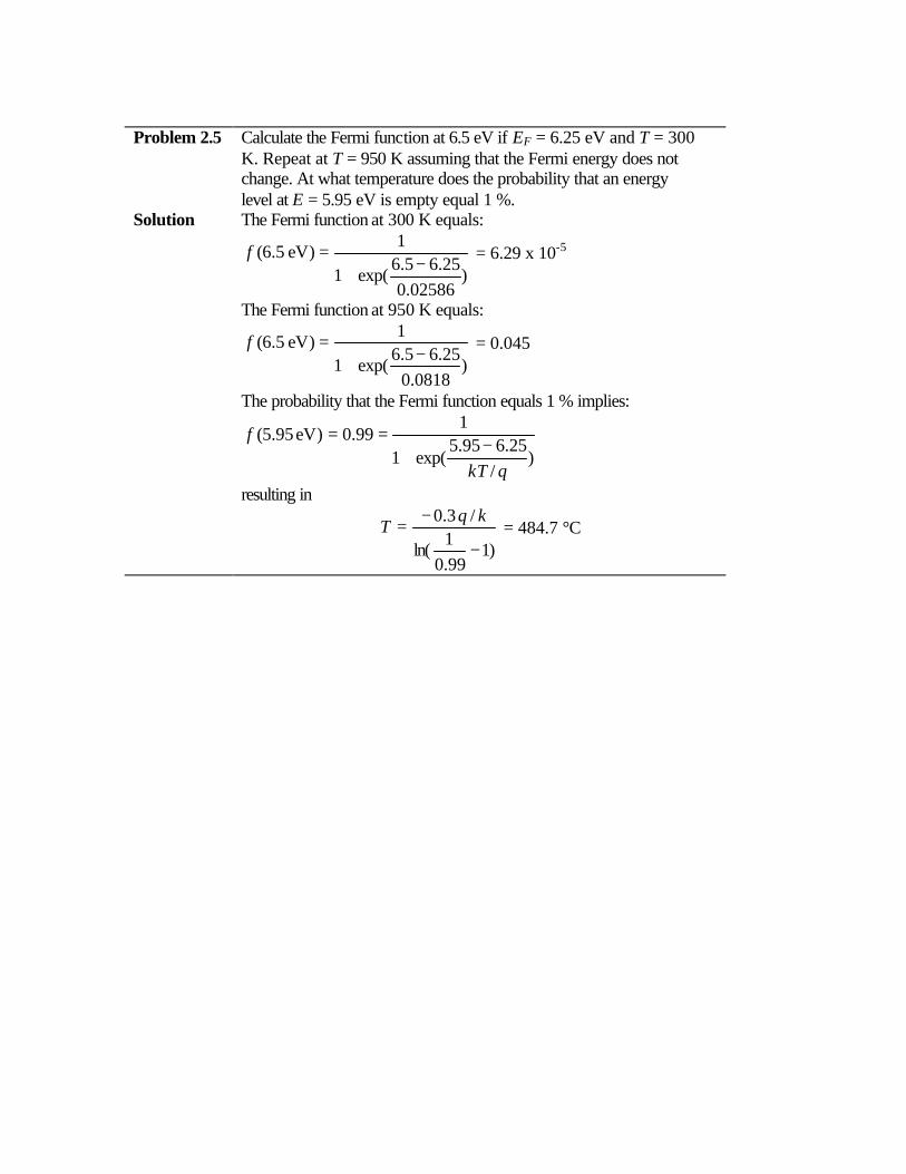
Problem 2.5 Calculate the Fermi function at 6.5 eV if EF = 6.25 eV and T = 300
K. Repeat at T = 950 K assuming that the Fermi energy does not change. At what temperature does the probability that an energy level at E = 5.95 eV is empty equal 1 %.
Solution The Fermi function at 300 K equals:
)02586.0
25.65.6exp(1
1)eV 5.6(
−+
=f = 6.29 x 10⁻⁵
The Fermi function at 950 K equals:
)0818.0
25.65.6exp(1
1)eV 5.6(
−+
=f = 0.045
The probability that the Fermi function equals 1 % implies:
)/
25.695.5exp(1
199.0)eV 95.5(
qkT
f−
+==
resulting in
)199.01
ln(
/3.0
−
−=
kqT = 484.7 °C
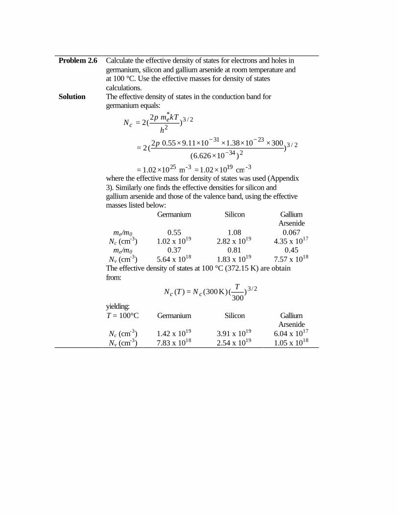
Problem 2.6 Calculate the effective density of states for electrons and holes in
germanium, silicon and gallium arsenide at room temperature and at 100 °C. Use the effective masses for density of states calculations.
Solution The effective density of states in the conduction band for germanium equals:
3-193-25
2/3234
2331
2/32
*
cm 1002.1m 1002.1
))10626.6(
3001038.11011.955.02(2
)2
(2
×=×=
×
×××××=
=
−
−−π
π
h
kTmN e
c
where the effective mass for density of states was used (Appendix 3). Similarly one finds the effective densities for silicon and gallium arsenide and those of the valence band, using the effective masses listed below:
Germanium Silicon Gallium Arsenide
me/m0 0.55 1.08 0.067
Nc (cm-3) 1.02 x 10¹⁹ 2.82 x 10¹⁹ 4.35 x 10¹⁷ me/m0 0.37 0.81 0.45
Nv (cm-3) 5.64 x 10¹⁸ 1.83 x 10¹⁹ 7.57 x 10¹⁸ The effective density of states at 100 °C (372.15 K) are obtain
from: 2/3)
300()K 300()(
TNTN cc =
yielding: T = 100°C Germanium Silicon Gallium
Arsenide Nc (cm-3) 1.42 x 10¹⁹ 3.91 x 10¹⁹ 6.04 x 10¹⁷
Nv (cm-3) 7.83 x 10¹⁸ 2.54 x 10¹⁹ 1.05 x 10¹⁸

Problem 2.7 Calculate the intrinsic carrier density in germanium, silicon and
gallium arsenide at room temperature (300 K). Repeat at 100 °C. Assume that the energy bandgap is independent of temperature and use the room temperature values.
Solution The intrinsic carrier density is obtained from:
)2
exp()(kT
ENNTn g
vci
−=
where both effective densities of states are also temperature dependent. Using the solution of Problem 2.6 one obtains: T = 300 K Germanium Silicon Gallium
Arsenide
ni (cm-3) 2.16 x 10¹³ 8.81 x 10⁹ 1.97 x 10⁶ T = 100°C Germanium Silicon Gallium
Arsenide
ni (cm-3) 3.67 x 10¹⁴ 8.55 x 10¹¹ 6.04 x 10⁸
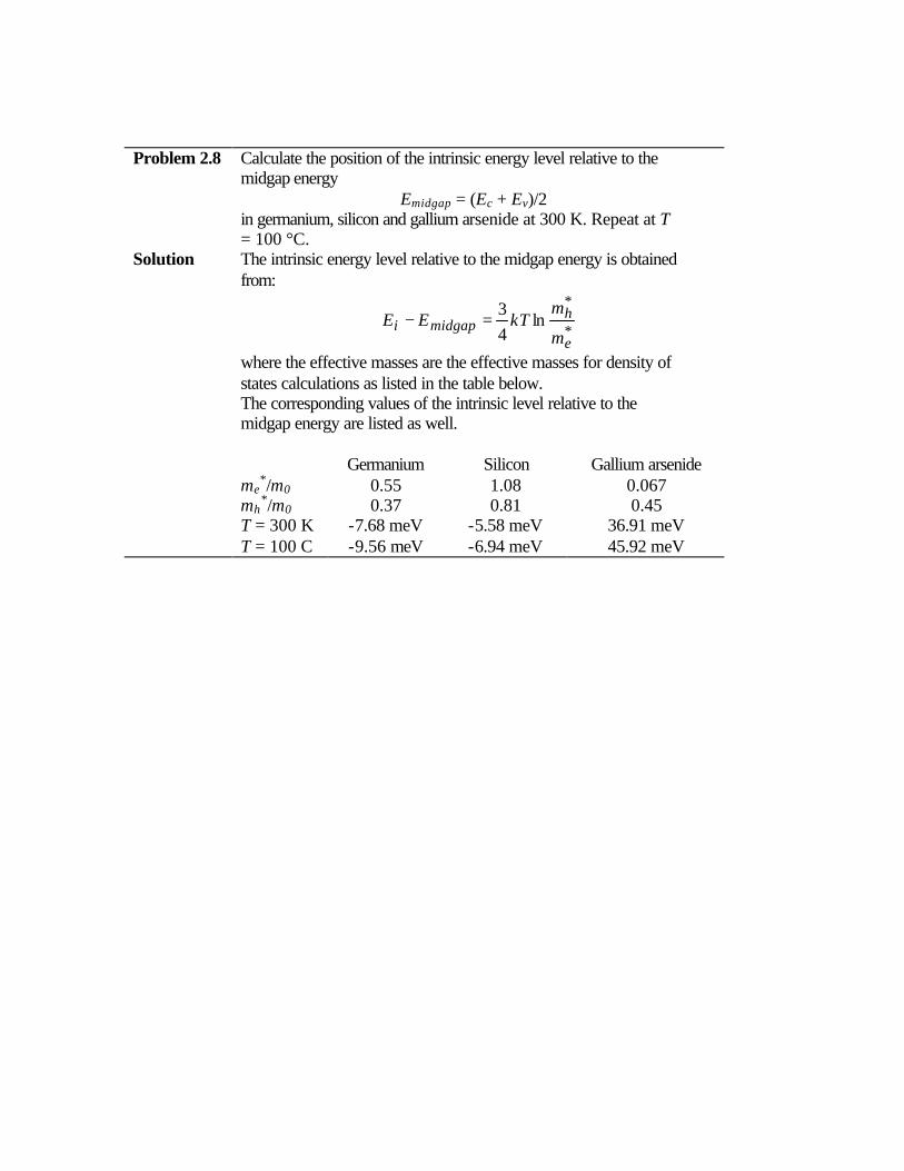
Problem 2.8 Calculate the position of the intrinsic energy level relative to the
midgap energy Emidgap = (Ec + Ev)/2
in germanium, silicon and gallium arsenide at 300 K. Repeat at T = 100 °C. The intrinsic energy level relative to the midgap energy is obtained from:
*
*ln
43
e
hmidgapi
m
mkTEE =−
where the effective masses are the effective masses for density of states calculations as listed in the table below. The corresponding values of the intrinsic level relative to the midgap energy are listed as well. Germanium Silicon Gallium arsenide me
*/m0 0.55 1.08 0.067 mh
*/m0 0.37 0.81 0.45 T = 300 K -7.68 meV -5.58 meV 36.91 meV
Solution
T = 100 C -9.56 meV -6.94 meV 45.92 meV

Problem 2.9 Calculate the electron and hole density in germanium, silicon and
gallium arsenide if the Fermi energy is 0.3 eV above the intrinsic energy level. Repeat if the Fermi energy is 0.3 eV below the conduction band edge. Assume that T = 300 K. The electron density, n, can be calculated from the Fermi energy using:
)02586.0
3.0exp(exp i
iFi n
kTEE
nn =−
=
and the corresponding hole density equals: p = ni
2/n the resulting values are listed in the table below. If the Fermi energy is 0.3 eV below the conduction band edge, one obtains the carrier densities using:
)02586.0
3.0exp(exp
−=
−= c
cFc N
kTEE
Nn
and the corresponding hole density equals: p = ni
2/n the resulting values are listed in the table below. Germanium Silicon Gallium
Arsenide ni (cm-3) 2.03 x 10¹³ 1.45 x 10¹⁰ 2.03 x 10⁶ Nc (cm-3) 1.02 x 10¹⁹ 6.62 x 10¹⁹ 4.37 x 10¹⁷
n (cm-3) 2.24 x 10¹⁸ 1.60 x 10¹⁵ 2.23 x 10¹¹ EF - Ei = 0.3 eV p (cm-3) 1.48 x 10⁸ 1.32 x 10⁵ 18.4
n (cm-3) 9.27 x 10¹³ 6.02 x 10¹⁴ 3.97 x 10¹²
Solution
EF - Ei = - 0.3 eV p (cm-3) 4.45 x 10¹² 3.50 x 10⁵ 1.04

Problem 2.10 The equations (2.6.34) and (2.6.35) derived in section 2.6 are only
valid for non-degenerate semiconductors (i.e. Ev + 3kT < EF < Ec - 3kT). Where exactly in the derivation was the assumption made that the semiconductor is non-degenerate?
Solution Equations (2.6.34) and (2.6.35) were derived using charge neutrality and the mass action law. Of those two assumptions, the use of the mass action law implies that the semiconductor is non-degenerate. The mass action law was derived using (2.6.12) and (2.6.13). These equations, representing a closed form solution for the thermal equilibrium carrier densities as a function of the Fermi energy, were in turn obtained by solving the Fermi integral and assuming that:
Ev + 3kT < EF < Ec - 3kT i.e. that the Fermi energy must be at least 3kT away from either bandedge and within the bandgap.
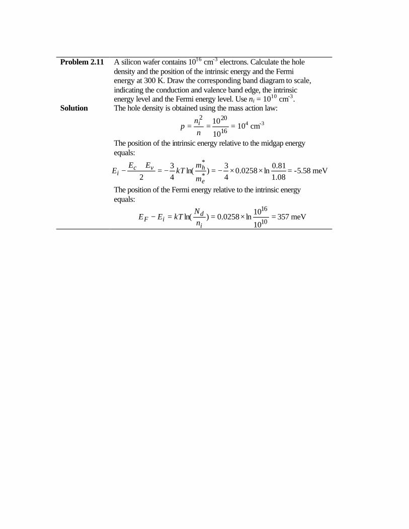
Problem 2.11 A silicon wafer contains 1016 cm-3 electrons. Calculate the hole
density and the position of the intrinsic energy and the Fermi energy at 300 K. Draw the corresponding band diagram to scale, indicating the conduction and valence band edge, the intrinsic energy level and the Fermi energy level. Use ni = 1010 cm-3.
Solution The hole density is obtained using the mass action law:
16
202
10
10==
nn
p i = 104 cm-3
The position of the intrinsic energy relative to the midgap energy equals:
08.181.0
ln0258.043
)ln(43
2 *
*××−=−=
+−
e
hvci
m
mkT
EEE = -5.58 meV
The position of the Fermi energy relative to the intrinsic energy equals:
=×==−10
16
10
10ln0258.0)ln(
i
diF n
NkTEE 357 meV

Problem 2.12 A silicon wafer is doped with 1013 cm-3 shallow donors and 9 x
1012 cm-3 shallow acceptors. Calculate the electron and hole density at 300 K. Use ni = 1010 cm-3.
Solution Since there are more donors than acceptors, the resulting material is n-type and the electron density equals the difference between the donor and acceptor density or:
n = Nd – Na = 1013 – 9 x 1012 = 1012 cm-3 The hole density is obtained by applying the mass action law:
12
202
10
10==
nn
p i = 108 cm-3
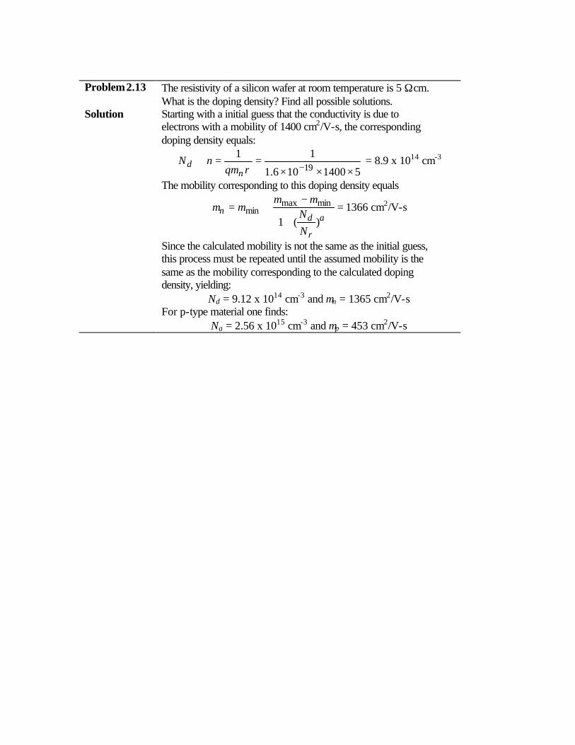
Problem 2.13 The resistivity of a silicon wafer at room temperature is 5 Ωcm.
What is the doping density? Find all possible solutions. Solution Starting with a initial guess that the conductivity is due to
electrons with a mobility of 1400 cm2/V-s, the corresponding doping density equals:
51400106.1
1119 ×××
==≅−ρµ n
d qnN = 8.9 x 1014 cm-3
The mobility corresponding to this doping density equals
=+
−+=
α
µµµµ
)(1
minmaxmin
r
dn
NN
1366 cm2/V-s
Since the calculated mobility is not the same as the initial guess, this process must be repeated until the assumed mobility is the same as the mobility corresponding to the calculated doping density, yielding:
Nd = 9.12 x 1014 cm-3 and µn = 1365 cm2/V-s For p-type material one finds:
Na = 2.56 x 1015 cm-3 and µp = 453 cm2/V-s

Problem 2.14 How many phosphorus atoms must be added to decrease the
resistivity of n-type silicon at room temperature from 1 Ω−cm to 0.1 Ω−cm. Make sure you include the doping dependence of the mobility. State your assumptions.
Solution Starting with a initial guess that the conductivity is due to electrons with a mobility of 1400 cm2/V-s, the corresponding doping density corresponding to the initial resistivity of 1 Ω−cm equals:
11400106.1
1119 ×××
==≅−ρµn
d qnN = 4.46 x 1015 cm-3
The mobility corresponding to this doping density equals
=+
−+=
α
µµµµ
)(1
minmaxmin
r
dn
NN
1274 cm2/V-s
Since the calculated mobility is not the same as the initial guess, this process must be repeated until the assumed mobility is the same as the mobility corresponding to the calculated doping density, yielding:
Nd,initial = 4.94 x 1015 cm-3 and µn = 1265 cm2/V-s Repeating this procedure for a resistivity of 0.1 Ω−cm one find the final doping density to be
Nd,final = 8.08 x 1016 cm-3 and µn = 772 cm2/V-s The added density of phosphorous atoms therefore equals
Nd, added = 4.94 x 10¹⁵ - = 7.59 x 1016 cm-3
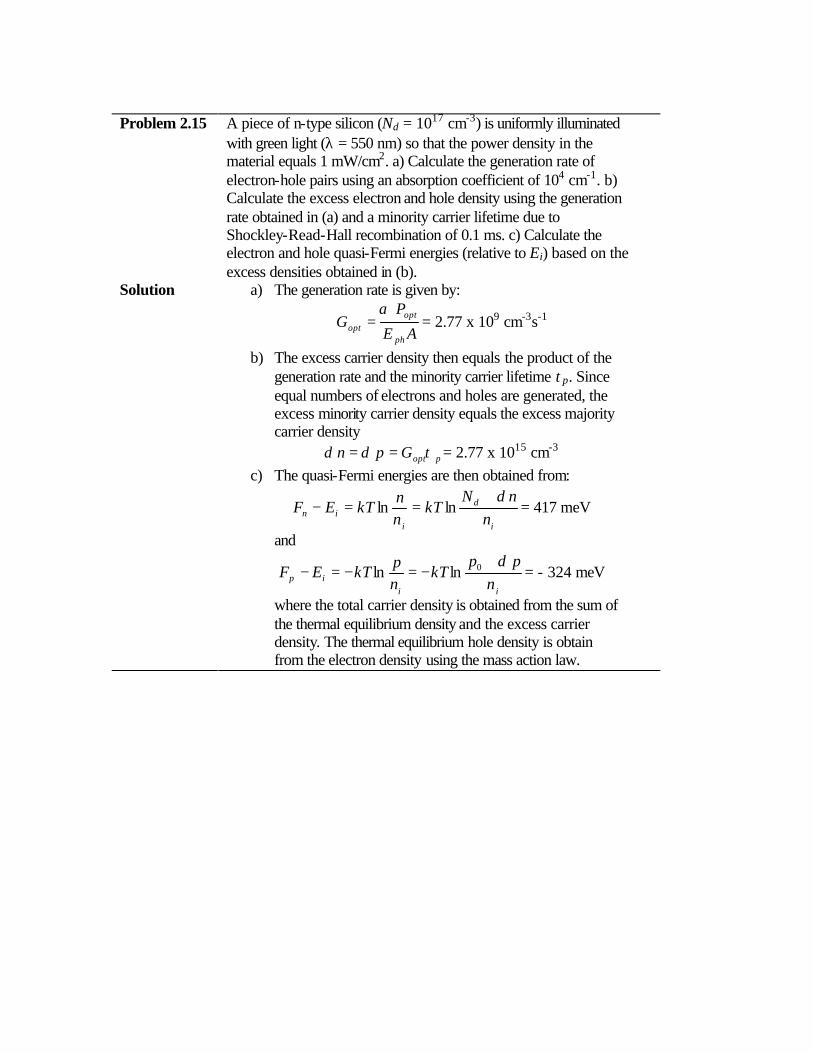
Problem 2.15 A piece of n-type silicon (Nd = 1017 cm-3) is uniformly illuminated
with green light (λ = 550 nm) so that the power density in the material equals 1 mW/cm2. a) Calculate the generation rate of electron-hole pairs using an absorption coefficient of 104 cm-1. b) Calculate the excess electron and hole density using the generation rate obtained in (a) and a minority carrier lifetime due to Shockley-Read-Hall recombination of 0.1 ms. c) Calculate the electron and hole quasi-Fermi energies (relative to Ei) based on the excess densities obtained in (b).
Solution a) The generation rate is given by:
AE
PG
ph
optopt
α= = 2.77 x 109 cm-3s-1
b) The excess carrier density then equals the product of the generation rate and the minority carrier lifetime τp. Since equal numbers of electrons and holes are generated, the excess minority carrier density equals the excess majority carrier density
poptGpn τδδ == = 2.77 x 1015 cm-3 c) The quasi-Fermi energies are then obtained from:
i
d
iin n
nNkT
nn
kTEFδ+
==− lnln = 417 meV
and
iiip n
ppkT
np
kTEFδ+
−=−=− 0lnln = - 324 meV
where the total carrier density is obtained from the sum of the thermal equilibrium density and the excess carrier density. The thermal equilibrium hole density is obtain from the electron density using the mass action law.
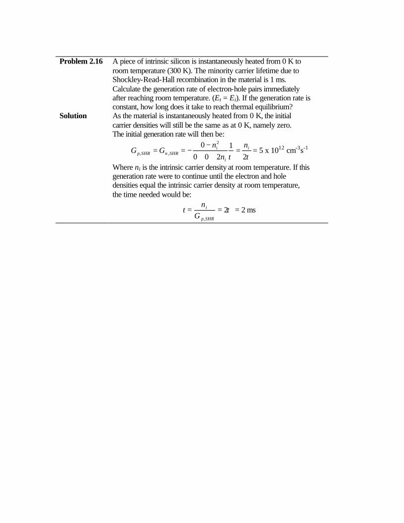
Problem 2.16 A piece of intrinsic silicon is instantaneously heated from 0 K to
room temperature (300 K). The minority carrier lifetime due to Shockley-Read-Hall recombination in the material is 1 ms. Calculate the generation rate of electron-hole pairs immediately after reaching room temperature. (Et = Ei). If the generation rate is constant, how long does it take to reach thermal equilibrium?
Solution As the material is instantaneously heated from 0 K, the initial carrier densities will still be the same as at 0 K, namely zero. The initial generation rate will then be:
ττ 21
2000 2
,,i
i
iSHRnSHRp
nn
nGG =
++−
−== = 5 x 1012 cm-3s-1
Where ni is the intrinsic carrier density at room temperature. If this generation rate were to continue until the electron and hole densities equal the intrinsic carrier density at room temperature, the time needed would be:
τ2,
==SHRp
i
Gn
t = 2 ms

Problem 2.17 Calculate the conductivity and resistivity of intrinsic silicon. Use
ni = 1010 cm-3, µn = 1400 cm2/V-sec and µp = 450 cm2/V-sec. Solution The conductivity of intrinsic silicon equals:
ipnpn nqpnq )()( µµµµσ +=+= = 2.96 µS/cm The resistivity is the inverse of the conductivity:
σρ
1= = 335 kΩ-cm

Problem 2.18 Consider the problem of finding the doping density, which
results in the maximum possible resistivity of silicon at room temperature. (ni = 1010 cm-3, µn = 1400 cm2/V-sec and µp = 450 cm2/V-sec.) Should the silicon be doped at all or do you expect the maximum resistivity when dopants are added? If the silicon should be doped, should it be doped with acceptors or donors (assume that all dopant are shallow). Calculate the maximum resistivity, the corresponding electron and hole density and the doping density.
Solution Since the mobility of electrons is larger than that of holes, one expects the resistivity to initially decrease as acceptors are added to intrinsic silicon. The maximum resistivity (or minimum conductivity) is obtained from:
0)/()( 2
=+
=+
=dn
nnndq
dn
pndq
dnd ipnpn µµµµσ
which yields:
in
pnn
µ
µ= = 0.57 ni = 5.7 x 109 cm-3
The corresponding hole density equals p = 1.76 ni = 1.76 x 109 cm-3 and the amount of acceptors one needs to add equals Na = 1.20 ni = 1.20 x 109 cm-3. The maximum resistivity equals:
15871
)(1
maxipn qnpnq
=+
=µµ
ρ = 394 kΩcm

Problem 2.19 The electron density in silicon at room temperature is twice the
intrinsic density. Calculate the hole density, the donor density and the Fermi energy relative to the intrinsic energy. Repeat for n = 5 ni and n = 10 ni. Also repeat for p = 2 ni, p = 5 ni and p = 10 ni, calculating the electron and acceptor density as well as the Fermi energy relative to the intrinsic energy level.
Solution The hole density is obtained using the mass action law: p = ni
2/n The doping density is obtained by requiring charge neutrality
Nd - Na = n - p The Fermi energy is obtained from:
EF - Ei = kT ln(n/ni) yielding:
n = 2 ni n = 5 ni n = 10 ni p ni /2 ni /5 ni /10
Nd - Na 1.5 ni 4.8 ni 9.9 ni EF - Ei kT ln(2)
= 18 meV kT ln(5)
= 42 meV kT ln(10) = 60 meV
p = 2 ni p = 5 ni p = 10 ni
n ni /2 ni /5 ni /10
Nd - Na -1.5 ni -4.8 ni -9.9 ni EF - Ei -kT ln(2)
= -18 meV -kT ln(5)
= -42 meV -kT ln(10) = -60 meV

Problem 2.20 The expression for the Bohr radius can also be applied to the
hydrogen-like atom consisting of an ionized donor and the electron provided by the donor. Modify the expression for the Bohr radius so that it applies to this hydrogen-like atom. Calculate the resulting radius of an electron orbiting around the ionized donor in silicon. (εr = 11.9 and me
* = 0.26 m0) Solution The Bohr radius is obtained from:
20
220
0qm
nha
π
ε=
However since the electron travel through silicon one has to replace the permittivity of vacuum with the dielectric constant of silicon and the free electron mass with the effective mass for conductivity calculations so that:
a0,donor in silicon 26.09.11
529/ 0
*0 ×==mm
ae
rε pm = 2.42 nm
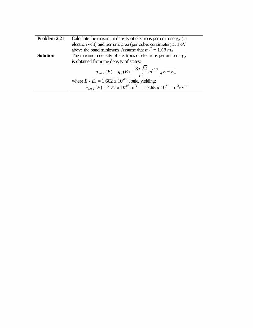
Problem 2.21 Calculate the maximum density of electrons per unit energy (in
electron volt) and per unit area (per cubic centimeter) at 1 eV above the band minimum. Assume that me
* = 1.08 m0 Solution The maximum density of electrons of electrons per unit energy
is obtained from the density of states:
ccMAX EEmh
EgEn −==2/3*
3
28)()(
π
where E - Ec = 1.602 x 10⁻¹⁹ Joule, yielding: =)(EnMAX 4.77 x 1046 m-3J-1 = 7.65 x 1021 cm-3eV-1
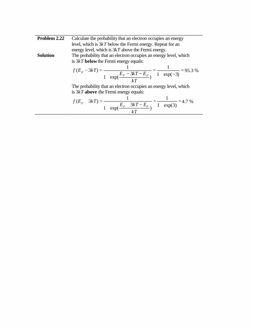
Problem 2.22 Calculate the probability that an electron occupies an energy
level, which is 3kT below the Fermi energy. Repeat for an energy level, which is 3kT above the Fermi energy.
Solution The probability that an electron occupies an energy level, which is 3kT below the Fermi energy equals:
=−+
=−−
+=−
)3exp(11
)3
exp(1
1)3(
kTEkTE
kTEfFF
F 95.3 %
The probability that an electron occupies an energy level, which is 3kT above the Fermi energy equals:
=+
=−+
+=+
)3exp(11
)3
exp(1
1)3(
kTEkTE
kTEfFF
F 4.7 %

Problem 2.23 Calculate and plot as a function of energy the product of the
probability that an energy level is occupied with the probability that that same energy level is not occupied. Assume that the Fermi energy is zero and that kT = 1 eV. Calculate the energy or energies for which the product of both probabilities is 10%
Solution The product of both probabilities can be written as: ))(1)(())(1)(()()( EfEfEfEfEfEf −−−=−=−
The product is therefore an even function and the maximum occurs at E = EF where the product is 25 % as can be seen on the figure:
The probability of the sum is therefore 10% for: 15.05.0)( ±=Ef = 11.7 % or 88.3 %
The corresponding values for the energies are 2.06 and –2.06 eV
0%
5%
10%
15%
20%
25%
30%
-6 -4 -2 0 2 4 6
E - E F (eV)
f(E
)f(-E
)

Problem 2.24 The effective mass of electrons in silicon is 0.26 m0 and the
effective mass of holes is 0.36 m0. If the scattering time is the same for both carrier types, what is the ratio of the electron mobility and the hole mobility.
Solution Since the mobility is related to the effective mass by:
mqτ
µ =
The ratio of the mobilities will be inversely proportional to the ratio of the effective masses, so that:
==26.036.0
p
n
µµ
1.39

Problem 2.25 Electrons in silicon carbide have a mobility of 1000 cm2/V-sec.
At what value of the electric field do the electrons reach a velocity of 3 x 107 cm/s? Assume that the mobility is constant and independent of the electric field. What voltage is required to obtain this field in a 5 micron thick region? How much time do the electrons need to cross the 5 micron thick region?
Solution The electric field is obtained from the mobility and the velocity:
7103
1400
×==
vµE = 30 kV/cm
Combined with the length one finds the applied voltage. V = E L = 30,000 x 5 x 10-4 = 15 V
The transit time equals the length divided by the velocity: tr = L/v = 5 x 10⁻⁴/3 x 107 = 16.7 ps

Problem 2.26 A piece of silicon has a resistivity which is specified by the
manufacturer to be between 2 and 5 Ohm cm. Assuming that the mobility of electrons is 1400 cm2/V-sec and that of holes is 450 cm2/V-sec, what is the minimum possible carrier density and what is the corresponding carrier type? Repeat for the maximum possible carrier density.
Solution The minimum carrier density is obtained for the highest resistivity and the material with the highest carrier mobility, i.e. the n-type silicon. The minimum carrier density therefore equals:
51400106.1
1119max ×××
==ρµ nq
n = 8.92 x 1014 cm-3
The maximum carrier density is obtained for the lowest resistivity and the material with the lowest carrier mobility, i.e. the p-type silicon. The maximum carrier density therefore equals:
2450106.1
1119min ×××
==ρµ pq
p = 6.94 x 1015 cm-3

Problem 2.27 A silicon wafer has a 2-inch diameter and contains 1014 cm-3
electrons with a mobility of 1400 cm2/V-sec. How thick should the wafer be so that the resistance between the front and back surface equals 0.1 Ohm?
Solution The resistance is given by
AL
R ρ=
Where A is the area of the wafer and L the thickness, so that the wafer thickness equals:
6.44)54.2(1.0 2××
==π
ρRA
L = 0.455 mm
The resistivity, r, was obtained from:
1419 101400106.1
11
×××==
nq nµρ = 44.6 Ω-cm

Problem 2.28 The electron mobility is germanium is 1000 cm2/V-sec. If this
mobility is due to impurity and lattice scattering and the mobility due to lattice scattering only is 1900 cm2/V-sec, what is the mobility due to impurity scattering only?
Solution The mobility is due to a combination of lattice and impurity scattering, namely:
s-/Vcm 100011
1 2=+
=
latticeimpurity
n
µµ
µ
so that the mobility due to impurity scattering only equals:
s-/Vcm 2111
19001
10001
1 2=−
=impurityµ
Problem 2.29 A piece of n-type silicon is doped with 1017 cm-3 shallow donors.
Calculate the density of electrons per unit energy at kT/2 above the conduction band edge. T = 300 K. Calculate the electron energy for which the density of electrons per unit energy has a maximum. What is the corresponding probability of occupancy at that maximum?

Solution The density of electrons per unit energy at a given energy equals:
)()()( EfEgEn c= where
cc EEh
mEg −=
3
2/328)(
π= 5.43 x 1039 cm-3J-1
and
kTEE
EfF−
+=
exp1
1)( = 9.14 x 10⁻⁴
The position of the Fermi energy is calculated from the doping density:
c
d
ccF N
NkT
Nn
kTEE lnln ==− = - 168 meV
This last equation is only valid if the semiconductor is non-degenerate, which is a justifiable assumption since the electron density is much smaller than the effective density of states. The Fermi function then becomes:
kTEE
kTEE
Ef F
F
−≅
−+
= expexp1
1)(
And the density of electrons per unit energy can then be further simplified to:
kTEE
EEh
mEfEgEn F
cc−
−≅= exp28
)()()(3
2/3π
The maximum is obtained by setting the derivative equal to zero:
0)(
=dE
Edn
This result in:
kTEE
EEkTkT
EE
EEF
cF
c
−−−
−
−= exp
1exp
121
0
Which can be solved to yield: E = Emax = Ec + kT/2
The corresponding probability of occupancy equals the value of the Fermi function calculated above. The corresponding electron density per unit energy is:
)()()( EfEgEn c= = 1.16 x 1037 cm-3 J-1

Problem 2.30 Phosphorous donor atoms with a concentration of 1016 cm-3 are
added to a piece of silicon. Assume that the phosphorous atoms are distributed homogeneously throughout the silicon. The atomic weight of phosphorous is 31.
a) What is the sample resistivity at 300 K? b) What proportion by weight does the donor impurity
comprise? The density of silicon is 2.33 gram/cm3. c) If 1017 atoms cm-3 of boron are included in addition to
phosphorous, and distributed uniformly, what is the resulting resistivity and type (i.e., p- or n-type material)?
d) Sketch the energy-band diagram under the condition of part c) and show the position of the Fermi energy relative to the valence band edge.

Solution a) The electron mobility in the silicon equals:
α
µµµµ
minmaxmin
)(1r
n
NN
+
−+= =
711.0
16
16)
102.9
10(1
5.6814145.68
×+
−+
= 1184 cm2/V-s
)(11
pnq pn µµσρ
+==
nq nµ1
≅ =
1619 101184106.1
1
××× − = 0.53 Ω-cm
b) Si ofdensity
volumeweight
volumeweight
SiP
P dA NMm≅
+
716327
101.2928.2
1010106.131 −×=××××=
c) The semiconductor is p-type since Na > Nd The hole density is obtained from:
22)2
(2 i
dada nNNNN
p +−
+−
=−+−+
21021616
)10()2109
(2109
+×
+×
= = 9 x 1016 cm-3
and the mobility is calculated from the sum of the donor and acceptor densities
α
µµµµ
minmaxmin
)(1r
p
NN
+
−+= =
719.0
17
16)
1023.2
1011(1
9.445.4709.44
×
×+
−+ = 310.6 cm2/V-s
leading to the conductivity of the material:
)(11
pnq pn µµσρ
+==
pq pµ1
≅ =
1619 1096.310106.1
1
×××× − = 0.22 Ω-cm
d) p
NkTEE v
vF ln=− =16
19
1091083.1ln0259.0
×× =137 meV

Problem 2.31 Find the equilibrium electron and hole concentrations and the
location of the Fermi energy relative to the intrinsic energy in silicon at 27 oC, if the silicon contains the following concentrations of shallow dopants.
a) 1 x 1016 cm-3 boron atoms b) 3 x 1016 cm-3 arsenic atoms and 2.9 x 1016 cm-3 boron
atoms. Solution a) Boron atoms are acceptors, therefore Na = 1016 cm-3
Since these are shallow acceptors and the material is not compensated, degenerate or close to intrinsic, the hole density equals the acceptor density:
p ≈ 1016 cm-3 Using the mass action law we then find the electron density
n = ni2/p = 1 x 104 cm-3
The Fermi energy is then obtained from:
iiF n
nkTEE ln=− =
10
4
10
10ln0259.0 = -357 meV
b) Arsenic atoms are donors, therefore Na = 2.9 x 1016 cm-3 and Nd = 3 x 1016 cm-3 Since these are shallow acceptors and the material is not degenerate or close to intrinsic, the electron density approximately equals the difference between the donor and acceptor density
n ≈ Nd – Na = 1015 cm-3 Using the mass action law we then find the hole density
p = ni2/n = 1 x 105 cm-3
The Fermi energy is then obtained from:
iiF n
nkTEE ln=− =
10
15
10
10ln0259.0 = 298 meV

Problem 2.32 The electron concentration in a piece of lightly doped, n-type
silicon at room temperature varies linearly from 1017 cm-3 at x = 0 to 6 x 1016 cm-3 at x = 2 µm. Electrons are supplied to keep this concentration constant with time. Calculate the electron current density in the silicon if no electric field is present. Assume µn = 1000 cm2/V-s and T = 300 K.
Solution The diffusion current is obtained from:
4
161719
102
106108.25106.1
−−
×
×−×××==
dxdn
qDJ nn = 828 A/cm2
where the diffusion constant Dn is obtained from: Dn = µn x Vt = 1000 x 0.0258 = 25.8 cm2
http://ece-www.colorado.edu/~bart/book/book/chapter2/ch2_r.htm
Title Page Table of Contents Help Copyright B. Van Zeghbroeck, 2004
Chapter 2: Semiconductor Fundamentals
Review Questions
1. Why do solids occur in the form of a crystal?
2. How do we classify the different crystals?
3. How many Bravais lattices are there in two dimensions? How many in three dimensions?
4. List the three cubic bravais lattices.
5. How do you explain that the allowed energies for electrons in solids are restricted to energy bands? Why are these bands separated energy band gaps? Why are the energies not discreet as in an atom. Why are they not continuous, as is the case for a free electron?
6. How does the conductivity of a solid depend on whether the energy bands are completely filled, partially filled or empty? How does the existence of overlapping bandgaps affect the conductivity?
7. Why does a completely filled band not contribute the conductivity of a solid?
8. Explain physically why the bandgap of a semiconductor decreases with temperature.
9. What are holes? Carefully justify your definition.
10. What is a state?
11. How many states are there in 1 micron sized cube for which an electron has a kinetic energy less than 1 eV? Treat the electron as a free electron confined to a box with infinite potential walls.
12. What is the physical meaning of the Fermi energy?
13. What is the value of the Fermi function at an energy, which is 3kT larger/lower than the Fermi energy?
14. What is the basic assumption used in statistical thermodynamics when calculating the probability distribution functions?
15. What are the two boundary conditions used to find the possible ways to fill energy levels with electrons.
16. How does a boson differ from a Fermion? Name two bosons.
17. List the assumptions made to obtain equations (2.6.12).
18. What is an intrinsic semiconductors? What is the hole density in an intrinsic semiconductor?
http://ece-www.colorado.edu/~bart/book/book/chapter2/ch2_r.htm (1 of 2)11/10/2004 16:34:57

http://ece-www.colorado.edu/~bart/book/book/chapter2/ch2_r.htm
19. Why is the product of the electron and hole density in a non-degenerate semiconductor constant rather than for instance the sum? This relationship is also referred to as the mass-action law. Why?
20. Define a non-degenerate semiconductor. Why do we need this concept?
21. What is the difference between a doped semiconductor and an extrinsic semiconductor?
22. What assumptions are made when deriving equations (2.6.29) and (2.6.30)?
23. Describe the temperature dependence of the carrier density in a semiconductor. Identify the three regions and explain what happens by indicating the filled and empty states on an energy band diagram. Do this for n-type, p-type and compensated material.
24. Name the two transport mechanisms in semiconductors.
25. Describe the microscopic behavior of electrons and holes in a semiconductor.
26. Define the mobility.
27. Explain why the mobility in a semiconductor depends on the doping density.
28. Define the resistivity and conductivity of a semiconductor.
29. Explain why the velocity in a semiconductor is limited.
30. What is the driving force, which causes diffusion?
31. Explain the relation between the mean free path, the scattering time and the thermal velocity.
32. List three recombination-generation mechanisms.
33. Explain why the net recombination rate as described by the simple model depends on the excess carrier density.
34. Describe the continuity equation in words.
35. What assumptions are made to obtain the diffusion equations (2.9.9) and (2.9.10) from the continuity equations (2.9.3) and (2.9.4)?
36. What is the diffusion length and how does it relate to the diffusion constant and the minority carrier lifetime?
37. What is the drift-diffusion model?
http://ece-www.colorado.edu/~bart/book/book/chapter2/ch2_r.htm (2 of 2)11/10/2004 16:34:57

http://ece-www.colorado.edu/~bart/book/book/chapter2/ch2_b.htm
Title Page Table of Contents Help Copyright B. Van Zeghbroeck, 2004
Chapter 2: Semiconductor Fundamentals
Bibliography
1. Physical Properties of crystals, J.F. Nye, Oxford University Press, 1979.
2. Crystal physics, H.J. Juretschke, W.A. Benjamin, Inc., 1974
3. Introduction to Solid State Physics, C. Kittel, Wiley & sons,
4. Electrons and holes in semiconductors, W. Shockley, D. Van Nostrand Company, 1959
5. Electrons in Solids Third edition, R.H. Bube, Academic Press, 1992.
6. Solid State Electronic Devices, Fourth edition, B. G. Streetman, Prentice Hall, 1995
7. Solid State Theory, W. A. Harrison, Dover publications, 1974
8. Thermal Physics, second edition, C. Kittel and H. Kroemer, Freeman, 1980
http://ece-www.colorado.edu/~bart/book/book/chapter2/ch2_b.htm11/10/2004 16:35:04

http://ece-www.colorado.edu/~bart/book/book/chapter2/ch2_g.htm
Title Page Table of Contents Help Copyright B. Van Zeghbroeck, 2004
Chapter 2: Glossary
Name
Acceptor An atom which is likely to take on one or more electrons when placed in a crystal Bandgap The range of energies between existing energy bands where no energy levels exist Compensation The process of adding donors and acceptor to a crystal Conduction band Lowest empty or partially filled band in a semiconductor Conductivity The ratio of the current density to the applied electric field
Continuity equation Equation which states that the rate of change of a density of particles equals the net flux of particles coming in
Crystal A solid which consists of atoms placed in a periodic arrangment Crystalline Made of one or multiple crystalsDensity of states The density of electronic states per unit energy and per unit volume Diffusion Motion of particles caused by thermal energy
Diffusion length Average distance minority carriers travel in a quasi-neutral region before they recombine
Donor An atom which is likely to give off one or more electrons when placed in a crystal Drift Motion of carriers caused by an electric field Energy band A collection of closely spaced energy levels Generation Process by which electron-hole pairs are generated Hole Particle associated with an empty electron level in an almost filled band Impurity A foreign atom in a crystal Intrinsic carrier density The density of electrons and holes in an intrinsic semiconductor Intrinsic semiconductor A semiconductors free of defects or impurities
Ionization The process of adding or removing an electron to/from an atom thereby creating a charged atom (i.e. ion)
Mass action law The law which describes the relation between the densities of species involved in a chemical reaction
Mobility The ratio of the carrier velocity to the applied electric field Recombination Process by which electron-hole pairs are removed Resistivity The ratio of the applied voltage to the current Saturation Velocity Maximum velocity which can be obtained in a specific semiconductor Valence band Highest filled or almost filled band in a semiconductor
http://ece-www.colorado.edu/~bart/book/book/chapter2/ch2_g.htm11/10/2004 16:35:10

Metal-Semiconductor Junctions
Title Page Table of Contents Help Copyright B. Van Zeghbroeck, 2004
Chapter 3: Metal-Semicond. Junctions
3.1 Introduction
Metal-to-semiconductor junctions are of great importance since they are present in every semiconductor device. They can behave either as a Schottky barrier or as an ohmic contact dependent on the characteristics of the interface. We will focus primarily on the Schottky barriers. This chapter contains an analysis of the electrostatics of the M-S junction. Calculated are the charge, field and potential distribution within the device. This chapter also contains a derivation of the current voltage characteristics due to diffusion, thermionic emission and tunneling in Metal-Semiconductor junctions.
http://ece-www.colorado.edu/~bart/book/book/chapter3/ch3_1.htm11/10/2004 16:35:55

Metal-Semicond. Junctions
Title Page Table of Contents Help Copyright B. Van Zeghbroeck, 2004
Chapter 3: Metal-Semicond. Junctions
3.2. Structure and principle of operation3.2.1. Structure3.2.2. Flatband diagram and built-in potential3.2.3. Thermal equilibrium3.2.4. Forward and reverse bias
3.2.1. Structure
The structure of a metal-semiconductor junction is shown in Figure 3.2.1. It consists of a metal contacting a piece of semiconductor. An ideal Ohmic contact, a contact such that no potential exists between the metal and the semiconductor, is made to the other side of the semiconductor. The sign convention of the applied voltage and current is also shown on Figure 3.2.1.
Figure 3.2.1 : Structure and sign convention of a metal-semiconductor junction
3.2.2. Flatband diagram and built-in potential
http://ece-www.colorado.edu/~bart/book/book/chapter3/ch3_2.htm (1 of 5)11/10/2004 16:36:09

Metal-Semicond. Junctions
The barrier between the metal and the semiconductor can be identified on an energy band diagram. To construct such diagram we first consider the energy band diagram of the metal and the semiconductor, and align them using the same vacuum level as shown in Figure 3.2.2 (a). As the metal and semiconductor are brought together, the Fermi energies of the metal and the semiconductor do not change right away. This yields the flatband diagram of Figure 3.2.2 (b).
Figure 3.2.2 : Energy band diagram of the metal and the semiconductor before (a) and after (b) contact is made.
The barrier height, φB, is defined as the potential difference between the Fermi energy of the metal and the band edge where the majority carriers reside. From Figure 3.2.2 (b) one finds that for an n-type semiconductor the barrier height is obtained from:
(3.2.1)
Where ΦM is the work function of the metal and χ is the electron affinity. The work function of selected metals as measured in vacuum can be found in Table 3.2.1. For p-type material, the barrier height is given by the difference between the valence band edge and the Fermi energy in the metal:
(3.2.2)
A metal-semiconductor junction will therefore form a barrier for electrons and holes if the Fermi energy of the metal as drawn on the flatband diagram is somewhere between the conduction and valence band edge.
In addition, we define the built-in potential, φI, as the difference between the Fermi energy of the metal and that of the semiconductor.
(3.2.3)
(3.2.4)
http://ece-www.colorado.edu/~bart/book/book/chapter3/ch3_2.htm (2 of 5)11/10/2004 16:36:09

Metal-Semicond. Junctions
The measured barrier height for selected metal-semiconductor junctions is listed in Table 3.2.1. These experimental barrier heights often differ from the ones calculated using (3.2.1) or (3.2.2). This is due to the detailed behavior of the metal-semiconductor interface. The ideal metal-semiconductor theory assumes that both materials are infinitely pure, that there is no interaction between the two materials nor is there an interfacial layer. Chemical reactions between the metal and the semiconductor alter the barrier height as do interface states at the surface of the semiconductor and interfacial layers. Some general trends however can still be observed. As predicted by (3.2.1), the barrier height on n-type semiconductors increases for metals with a higher work function as can be verified for silicon. Gallium arsenide on the other hand is known to have a large density of surface states so that the barrier height becomes virtually independent of the metal. Furthermore, one finds the barrier heights reported in the literature to vary widely due to different surface cleaning procedures.
Table 3.2.1: Workfunction of selected metals and their measured barrier height on germanium, silicon and gallium arsenide.
Example 3.1 Consider a chrome-silicon metal-semiconductor junction with Nd = 1017 cm-3. Calculate the barrier height and the built-in potential. Repeat for a p-type semiconductor with the same doping density.
Solution The barrier height equals:
Note that this value differs from the one listed in Table 3.2.1 since the work function in vacuum was used. See the discussion in the text for more details.
The built-in potential equals:
The barrier height for the chrome/p-silicon junction equals:
http://ece-www.colorado.edu/~bart/book/book/chapter3/ch3_2.htm (3 of 5)11/10/2004 16:36:09
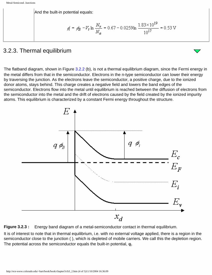
Metal-Semicond. Junctions
And the built-in potential equals:
3.2.3. Thermal equilibrium
The flatband diagram, shown in Figure 3.2.2 (b), is not a thermal equilibrium diagram, since the Fermi energy in the metal differs from that in the semiconductor. Electrons in the n-type semiconductor can lower their energy by traversing the junction. As the electrons leave the semiconductor, a positive charge, due to the ionized donor atoms, stays behind. This charge creates a negative field and lowers the band edges of the semiconductor. Electrons flow into the metal until equilibrium is reached between the diffusion of electrons from the semiconductor into the metal and the drift of electrons caused by the field created by the ionized impurity atoms. This equilibrium is characterized by a constant Fermi energy throughout the structure.
Figure 3.2.3 : Energy band diagram of a metal-semiconductor contact in thermal equilibrium.It is of interest to note that in thermal equilibrium, i.e. with no external voltage applied, there is a region in the semiconductor close to the junction ( ), which is depleted of mobile carriers. We call this the depletion region. The potential across the semiconductor equals the built-in potential, φi.
http://ece-www.colorado.edu/~bart/book/book/chapter3/ch3_2.htm (4 of 5)11/10/2004 16:36:09

Metal-Semicond. Junctions
3.2.4. Forward and reverse bias
Operation of a metal-semiconductor junction under forward and reverse bias is illustrated with Figure 3.2.4. As a positive bias is applied to the metal (Figure 3.2.4 (a)), the Fermi energy of the metal is lowered with respect to the Fermi energy in the semiconductor. This results in a smaller potential drop across the semiconductor. The balance between diffusion and drift is disturbed and more electrons will diffuse towards the metal than the number drifting into the semiconductor. This leads to a positive current through the junction at a voltage comparable to the built-in potential.
Figure 3.2.4 : Energy band diagram of a metal-semiconductor junction under (a) forward and (b) reverse biasAs a negative voltage is applied (Figure 3.2.4 (b)), the Fermi energy of the metal is raised with respect to the Fermi energy in the semiconductor. The potential across the semiconductor now increases, yielding a larger depletion region and a larger electric field at the interface. The barrier, which restricts the electrons to the metal, is unchanged so that the flow of electrons is limited by that barrier independent of the applied voltage. The metal-semiconductor junction with positive barrier height has therefore a pronounced rectifying behavior. A large current exists under forward bias, while almost no current exists under reverse bias.
The potential across the semiconductor therefore equals the built-in potential, φi, minus the applied voltage, Va.
(3.2.5)
http://ece-www.colorado.edu/~bart/book/book/chapter3/ch3_2.htm (5 of 5)11/10/2004 16:36:09
Electrostatic analysis
Title Page Table of Contents Help Copyright B. Van Zeghbroeck, 2004
Chapter 3: Metal-Semicond. Junctions
3.3. Electrostatic analysis3.3.1. General discussion - Poisson's equation3.3.2. Full depletion approximation3.3.3. Full depletion analysis3.3.4. Junction capacitance3.3.5. Schottky barrier lowering3.3.6. Derivation of Schottky barrier lowering 3.3.7. Solution to Poison's equation
3.3.1. General discussion - Poisson's equation
The electrostatic analysis of a metal-semiconductor junction is of interest since it provides knowledge about the charge and field in the depletion region. It is also required to obtain the capacitance-voltage characteristics of the diode.The general analysis starts by setting up Poisson's equation:
(3.3.1)
where the charge density, ρ, is written as a function of the electron density, the hole density and the donor and acceptor densities. To solve the equation, we have to express the electron and hole density, n and p, as a function of the potential, φ, yielding:
(3.3.2)
with
(3.3.3)
where the potential is chosen to be zero in the n-type region, where x >> xn.
This second-order non-linear differential equation (3.3.2) can not be solved analytically. Instead we will make the simplifying assumption that the depletion region is fully depleted and that the adjacent neutral regions contain no charge. This full depletion approximation is the topic of section 3.3.2.
http://ece-www.colorado.edu/~bart/book/book/chapter3/ch3_3.htm (1 of 7)11/10/2004 16:36:21

Electrostatic analysis
3.3.2. Full depletion approximation
The simple analytic model of the metal-semiconductor junction is based on the full depletion approximation. This approximation is obtained by assuming that the semiconductor is fully depleted over a distance xd, called the depletion region. While this assumption does not provide an accurate charge distribution, it does provide very reasonable approximate expressions for the electric field and potential throughout the semiconductor. These are derived in section 3.3.3.
3.3.3. Full depletion analysis
We now apply the full depletion approximation to an M-S junction containing an n-type semiconductor. We define the depletion region to be between the metal-semiconductor interface (x = 0) and the edge of the depletion region (x = xd). The depletion layer width, xd, is unknown at this point but will later be expressed as a function of the applied voltage.To find the depletion layer width, we start with the charge density in the semiconductor and calculate the electric field and the potential across the semiconductor as a function of the depletion layer width. We then solve for the depletion layer width by requiring the potential across the semiconductor to equal the difference between the built-in potential and the applied voltage, φi - Va. The different steps of the analysis are illustrated by Figure 3.3.1.
As the semiconductor is depleted of mobile carriers within the depletion region, the charge density in that region is due to the ionized donors. Outside the depletion region, the semiconductor is assumed neutral. This yields the following expressions for the charge density, ρ:
(3.3.4)
where we assumed full ionization so that the ionized donor density equals the donor density, Nd. This charge density is shown in Figure 3.3.1 (a). The charge in the semiconductor is exactly balanced by the charge in the metal, QM, so that no electric field exists except around the metal-semiconductor interface.
http://ece-www.colorado.edu/~bart/book/book/chapter3/ch3_3.htm (2 of 7)11/10/2004 16:36:21

Electrostatic analysis
Figure 3.3.1 : (a) Charge density, (b) electric field, (c) potential and (d) energy as obtained with the full depletion analysis.
Using Gauss's law we obtain electric field as a function of position, also shown in Figure 3.3.1 (b):
(3.3.5)
where εs is the dielectric constant of the semiconductor. We also assumed that the electric field is zero outside the depletion region. It is expected to be zero there since a non-zero field would cause the mobile carriers to redistribute until there is no field. The depletion region does not contain mobile carriers so that there can be an electric field. The largest (absolute) value of the electric field is obtained at the interface and is given by:
(3.3.6)
where the electric field was also related to the total charge (per unit area), Qd, in the depletion layer. Since the electric field is minus the gradient of the potential, one obtains the potential by integrating the expression for the electric field, yielding:
http://ece-www.colorado.edu/~bart/book/book/chapter3/ch3_3.htm (3 of 7)11/10/2004 16:36:21

Electrostatic analysis
(3.3.7)
We now assume that the potential across the metal can be neglected. Since the density of free carriers is very high in a metal, the thickness of the charge layer in the metal is very thin. Therefore, the potential across the metal is several orders of magnitude smaller that that across the semiconductor, even though the total amount of charge is the same in both regions.
The total potential difference across the semiconductor equals the built-in potential, φi, in thermal equilibrium and is further reduced/increased by the applied voltage when a positive/negative voltage is applied to the metal as described by equation (3.2.5). This boundary condition provides the following relation between the semiconductor potential at the surface, the applied voltage and the depletion layer width:
(3.3.8)
Solving this expression for the depletion layer width, xd, yields:
(3.3.9)
3.3.4. Junction capacitance
In addition, we can obtain the capacitance as a function of the applied voltage by taking the derivative of the charge with respect to the applied voltage yielding:
(3.3.10)
The last term in the equation indicates that the expression of a parallel plate capacitor still applies. One can understand this once one realizes that the charge added/removed from the depletion layer as one decreases/increases the applied voltage is added/removed only at the edge of the depletion region. While the parallel plate capacitor expression seems to imply that the capacitance is constant, the metal-semiconductor junction capacitance is not constant since the depletion layer width, xd, varies with the applied voltage.
Example 3.2 Consider a chrome-silicon metal-semiconductor junction with Nd = 1017 cm-3. Calculate the depletion layer width, the electric field in the silicon at the metal-semiconductor interface, the potential across the semiconductor and the capacitance per unit area for an applied voltage of -5 V.
http://ece-www.colorado.edu/~bart/book/book/chapter3/ch3_3.htm (4 of 7)11/10/2004 16:36:21

Electrostatic analysis
Solution The depletion layer width equals:
where the built-in potential was already calculated in Example 3.1.
The electric field in the semiconductor at the interface is:
The potential equals:
And the capacitance per unit area is obtained from:
3.3.5. Schottky barrier lowering
Image charges build up in the metal electrode of a metal-semiconductor junction as carriers approach the metal-semiconductor interface. The potential associated with these charges reduces the effective barrier height. This barrier reduction tends to be rather small compared to the barrier height itself. Nevertheless this barrier reduction is of interest since it depends on the applied voltage and leads to a voltage dependence of the reverse bias current. Note that this barrier lowering is only experienced by a carrier while approaching the interface and will therefore not be noticeable in a capacitance-voltage measurement. An energy band diagram of an n-type silicon Schottky barrier including the barrier lowering is shown in Figure 3.3.2:
http://ece-www.colorado.edu/~bart/book/book/chapter3/ch3_3.htm (5 of 7)11/10/2004 16:36:21

Electrostatic analysis
Figure 3.3.2: Energy band diagram of a silicon Schottky barrier with φB = 0.8 V and Nd = 1019 cm-3.
Shown is the energy band diagram obtained using the full-depletion approximation, the potential reduction experienced by electrons, which approach the interface and the resulting conduction band edge. A rounding of the conduction band edge can be observed at the metal-semiconductor interface as well as a reduction of the height of the barrier.The calculation of the barrier reduction assumes that the charge of an electron close to the metal-semiconductor interface attracts an opposite surface charge, which exactly balances the electron's charge so that the electric field surrounding the electron does not penetrate beyond this surface charge. The time to build-up the surface charge and the time to polarize the semiconductor around the moving electron is assumed to be much shorter than the transit time of the electron . This scenario is based on the assumption that there are no mobile or fixed charges around the electron as it approaches the metal-semiconductor interface. The electron and the induced surface charges are shown in Figure 3.3.3:
Figure 3.3.3: a) Field lines and surface charges due to an electron in close proximity to a perfect conductor and b) the field lines and image charge of an electron.
It can be shown that the electric field in the semiconductor is identical to that of the carrier itself and another carrier with opposite charge at equal distance but on the opposite side of the interface. This charge is called the image charge. The difference between the actual surface charges and the image charge is that the fields in the metal are distinctly different. The image charge concepts is justified on the basis that the electric field lines are perpendicular to the surface a perfect conductor, so that, in the case of a flat interface, the mirror image of the field lines provides continuous field lines across the interface. The barrier lowering depends on the square root of the electric field at the interface and is calculated from:
http://ece-www.colorado.edu/~bart/book/book/chapter3/ch3_3.htm (6 of 7)11/10/2004 16:36:21
Electrostatic analysis
(3.3.11)
http://ece-www.colorado.edu/~bart/book/book/chapter3/ch3_3.htm (7 of 7)11/10/2004 16:36:21

3.3.6. Derivation of Schottky barrier lowering
We now derive this equation by calculating the potential due to the image charge and adding it to the potential within the depletion region.
The electrostatic force between the two particles, one with a positive electronic charge and the other with a negative electronic charge, which are both a distance, x, away from the interface at x = 0, is given by:
2
2
)2(4)()(
xqxqxF
sI πε
−== E (3.3.12)
The corresponding potential equals:
xqdxxx
sxI πε
φ16
)()( =−= ∫∞
E (3.3.13)
which combined with the potential variation due to the electric field yields the following potential energy, V(x), versus position, x:
x
qxqqxV
sB πε
φ16
)( max −−−= E (3.3.14)
where the field due to the charge in the depletion region is assumed to be constant and set equal to the maximum field, Emax:
s
aid VqNεφ )(2
max
−=E
(3.3.15)
At this point the question arises why a single electron can noticeably alter the potential, while the depletion layer contains significantly more charge. To understand this, one has to realize that we have assumed that the charge in the depletion region is not quantized, but instead is distributed throughout the depletion layer. While this assumption does provide the correct average potential it does not accurately reflect the potential variations due to the individual charges of the ionized donors or mobile electrons. As we assumed that the single electron is far away from all other charges in the semiconductor, the potential energy due to all those charges is close to the average potential energy.
The potential energy due to the distributed charge of the ionized donors and a single electron reaches its maximum value at:
maxmax 16 Es
qxπε
= (3.3.16)

and the corresponding maximum value of the potential energy equals:
BB qqV φφ ∆−=max (3.3.17)
where ∆φB is the barrier height reduction given by:
sB
qπε
φ4
maxE=∆
(3.3.18)
3.3.7. Solution to Poisson’s Equation
To assess the error made when using the full depletion approximation we now derive the correct solution by solving Poisson's equation analytically2. The actual solution for the potential is then obtained by numerically integrating the expression for the electric field. We start from the charge density, ρ, in a semiconductor for the general case where electrons, holes, ionized acceptors and ionized donors are present:
)()( −+ −−+= ad NnNpqφρ (3.3.19)
Where φ is the potential in the semiconductor. The potential is chosen to equal zero deep into the semiconductor. For an n-type semiconductor without acceptors or free holes this can be further reduced to:
))exp(1()(
kTq
qNdφ
φρ −= (3.3.20)
assuming the semiconductor to be non-degenerate and fully ionized. A similar expression can be obtained for p-type material. Poisson's law can then be rewritten as:
))exp(1(
)(2
2
kTq
qNdxd
ds
φεφρφ
−−=−= (3.3.21)
Multiplying both sides with dφ/dx, this equation can be integrated between an arbitrary point x and infinity. The electric field at infinity (deep in the semiconductor) is taken to be zero. The electric field for a given potential is then:
]1)()[exp(2)())exp(1(2)(
0
−−=−−
= ∫ttD
t
s
d
VVLV
signdkTqqN φφ
φφφ
εφ
φ
E
(3.3.22)
Where the sign function equals +1 or -1 depending on the sign of φ and LD is the Debye length
given by, d
sD Nq
kTL 2
ε= . Equation (3.3.22) is plotted in Figure 3.3.4 using normalized
parameters. Depletion occurs for negative potentials while accumulation occurs for positive potentials.
2This derivation follows that of Goodman and Perkins, J. Appl. Phys. 35, p 3351, 1964.

Normalized Potential
Nor
mal
ized
Fie
ld
0.01
0.1
1
10
100
1000
10000
100000
-100 -80 -60 -40 -20 0 20
Figure 3.3.4 Absolute value of the normalized electric field, |E| LD/Vt, versus normalized potential, φ/Vt
Applying Gauss's law (Q = εsE) we the find the relation between the total charge in the semiconductor region and the total potential across the semiconductor. The capacitance can also be obtained from:
]1)()[exp(2
1)exp(
−−
−===
tt
t
D
s
as
a
VV
VLdV
ddVdQ
Cφφ
φε
εE
(3.3.23)
where φs is the potential across the semiconductor and equals -φi + Va. This expression can be approximated for φs< 0 and |φs| >> Vt yielding:
)(22
1
tai
ds
t
taiD
s
VVqN
VVVL
C−−
=−−
=φ
εφ
ε
(3.3.24)
This expression equals (3.3.10) as derived using the full depletion approximation, except for the added term, Vt, in the denominator. This expression yields the capacitance value with a relative accuracy better than 0.3 % for Va < φi – 6Vt.

3.3.7.1.Numeric solution
A numeric solution can be obtained by integrating equation (3.3.21). The solution to the energy band diagram, the charge density, the electric field and the potential are shown in the figures below: Integration was started four Debye lengths to the right of the edge of the depletion region as obtained using the full depletion approximation. Initial conditions were obtained by assuming the potential at the starting point to be adequately expressed by a solution to the homogenous equation:
−−=
D
dt L
xxV
)(expφ
(3.3.25)
Shown are solutions for a gold-silicon M-S junction with ΦM = 4.75V, χ = 4.05V, Nd = 1016 cm-3 and εs/ε0 = 11.9.
Distance [micron]
Ene
rgy
[eV
]
-1
-0.5
0
0.5
1
1.5
-0.2 -0.1 0 0.1 0.2 0.3 0.4 0.5 0.6
Ec
Ev
Ei
Efm
Efn
Figure 3.3.5 Energy band diagram of an M-S junction
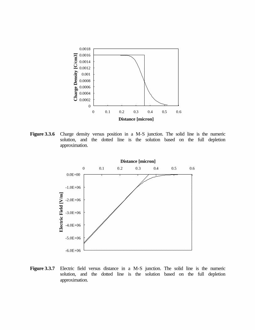
Distance [micron]
Cha
rge
Den
sity
[C/c
m3]
0
0.0002
0.0004
0.0006
0.0008
0.001
0.0012
0.0014
0.0016
0.0018
0 0.1 0.2 0.3 0.4 0.5 0.6
Figure 3.3.6 Charge density versus position in a M-S junction. The solid line is the numeric solution, and the dotted line is the solution based on the full depletion approximation.
Distance [micron]
Ele
ctri
c F
ield
[V/m
]
-6.0E+06
-5.0E+06
-4.0E+06
-3.0E+06
-2.0E+06
-1.0E+06
0.0E+00
0 0.1 0.2 0.3 0.4 0.5 0.6
Figure 3.3.7 Electric field versus distance in a M-S junction. The solid line is the numeric solution, and the dotted line is the solution based on the full depletion approximation.

Distance [micron]
Pote
ntia
l [V
]
-1-0.9-0.8-0.7-0.6-0.5-0.4-0.3-0.2-0.1
00 0.1 0.2 0.3 0.4 0.5 0.6
Figure 3.3.8 Potential versus distance of an M-S junction. The solid line is the numeric solution, and the dotted line is the solution based on the full depletion approximation.
3.3.7.2. Depletion at the Metal-Semiconductor interface
Most metal semiconductor contacts have a depletion region adjacent to the interface. We distinguish between the case where a large potential variation is found across the semiconductor, for which only a small correction is obtained compared to the full depletion approximation, and the case where a small potential variation exists across the semiconductor, for which the full depletion approximation does not apply.
3.3.7.2.1. Large potential approximation
If the potential difference across the semiconductor is larger than the thermal voltage, or φs = Va - φi < 0 and |Va - φi| >> kT/q we find the effective depletion layer width, xd, defined as the ratio of the total depletion layer charge to the charge density of the fully ionized donors, to be:
−−==
t
taiD
d
dd V
VVL
qNQ
xφ
2 (3.3.26)
where LD is the extrinsic Debye length of the semiconductor, which is given by:
d
sD Nq
kTL 2
ε=
(3.3.27)
The small signal capacitance can be expressed by:
d
s
tai
t
D
s
a
d
xVVV
LdVdQ
Cε
φε
=−−
==)(2
(3.3.28)
where Qd is the total charge per unit area in the depletion layer. This result differs from the one obtained by using the full depletion approximation in that the applied voltage is increased by the thermal voltage. However the capacitance is still the ratio of the dielectric constant to the depletion layer width.
3.3.7.2.2. Small potential approximation
If the potential difference across the semiconductor is smaller than the thermal voltage, or φ = Va
- φi < 0 and |Va - φi| < kT/q, the depletion layer width is proportional to the Debye length and the applied voltage:
t
aiDd V
VLx
−=
φ
(3.3.29)
and the capacitance is constant, independent of the applied voltage:
D
s
LC ε=
(3.3.30)
3.3.7.3.Accumulation at the Metal-Semiconductor interface
Accumulation occurs at the semiconductor metal interface if the Fermi energy of the metal lies between the conduction band edge and the Fermi energy in the n-type semiconductor, or Φs >
ΦM > χ. A similar condition can be defined for p-type material. Equation [3.1.10] applies for depletion as well as accumulation. However it does not provide a solution for the electric field and potential as a function of position. Instead we start again from the integral formulation of equation [3.1.10] but set the potential equal to zero at the interface and integrate from 0 to x. We also assume that the electron concentration at the surface, ns is much larger than the donor concentration. Using this convention, equation [3.1.10] can be rewritten as:
dxd
kTqkTn
s
s φφε
φ −== )2
exp(2
)(E (3.3.31)
integrating this equation again from 0 to x yields:
]1)
2[exp(2
2−−=
tt
s
sV
VxkTqn φ
ε
(3.3.32)
from which the charge density can be obtained:

2)2
1()exp()(
D
s
ts
Lx
qnV
qnx+
−=−=
φρ
(3.3.33)
Integration of the charge density yields the electric field.
D
D
LxqL
kTx
21
12)(
+=E
(3.3.34)
The width of the accumulation layer is obtained by solving the expression for the potential for x with φ(xd) = φi – Va.
]1)
2[exp(2 −
−=
t
aiDd V
VLx
φ
(3.3.35)
The correct solution can also be obtained by integrating [3.1.10]. A solution for a M-S junction with ΦM = 4.2V, χ = 4.05V, Nd = 1016 cm-3 and εs/ε0 = 11.9 is shown in the figures below.

-0.02
-0.015
-0.01
-0.005
0
Charge Density [C/cm3]
Ele
ctri
c F
ield
[V/m
]
0.0E+00
5.0E+05
1.0E+06
1.5E+06
2.0E+06
2.5E+06
Pot
enti
al [V
]
00.010.020.030.040.050.060.07
D i s t a n c e [ m i c r o n ]
Ene
rgy
[eV
]
- 1
- 0 . 8
- 0 . 6
- 0 . 4
- 0 . 2
0
0 . 2
0 . 4
- 0 . 0 5 0 0 . 0 5 0 . 1 0 . 1 5 0 . 2
E c
E v
E i
E f m E f n
Figure 3.3.9 Charge density, electric field, potential and energy band diagram of a metal-
semiconductor junction

Schottky diode current
Title Page Table of Contents Help Copyright B. Van Zeghbroeck, 2004
Chapter 3: Metal-Semicond. Junctions
3.4. Schottky diode current3.4.1. Diffusion current3.4.2. Thermionic emission3.4.3. Tunneling3.4.4. Derivation of the M-S junction current
The current across a metal-semiconductor junction is mainly due to majority carriers. Three distinctly different mechanisms exist: diffusion of carriers from the semiconductor into the metal, thermionic emission of carriers across the Schottky barrier and quantum-mechanical tunneling through the barrier. The diffusion theory assumes that the driving force is distributed over the length of the depletion layer. The thermionic emission theory on the other hand postulates that only energetic carriers, those, which have an energy equal to or larger than the conduction band energy at the metal-semiconductor interface, contribute to the current flow. Quantum-mechanical tunneling through the barrier takes into account the wave-nature of the electrons, allowing them to penetrate through thin barriers. In a given junction, a combination of all three mechanisms could exist. However, typically one finds that only one limits the current, making it the dominant current mechanism.The analysis reveals that the diffusion and thermionic emission currents can be written in the following form:
(3.4.1)
This expression states that the current is the product of the electronic charge, q, a velocity, v, and the density of available carriers in the semiconductor located next to the interface. The velocity equals the mobility multiplied with the field at the interface for the diffusion current and the Richardson velocity (see section 3.4.2) for the thermionic emission current. The minus one term ensures that the current is zero if no voltage is applied as in thermal equilibrium any motion of carriers is balanced by a motion of carriers in the opposite direction. The tunneling current is of a similar form, namely:
(3.4.2)
where vR is the Richardson velocity and n is the density of carriers in the semiconductor. The tunneling probability term, Θ, is added since the total current depends on the carrier flux arriving at the tunnel barrier multiplied with the probability, Θ, that they tunnel through the barrier.
3.4.1. Diffusion current
This analysis assumes that the depletion layer is large compared to the mean free path, so that the concepts of drift and diffusion are valid. The resulting current density equals:
(3.4.3)
http://ece-www.colorado.edu/~bart/book/book/chapter3/ch3_4.htm (1 of 3)11/10/2004 16:37:55

Schottky diode current
The current therefore depends exponentially on the applied voltage, Va, and the barrier height, φB. The prefactor can more easily be understood if one rewrites it as a function of the electric field at the metal-semiconductor interface, max:
(3.4.4)
yielding:
(3.4.5)
so that the prefactor equals the drift current at the metal-semiconductor interface, which for zero applied voltage exactly balances the diffusion current.
3.4.2 Thermionic emission
The thermionic emission theory assumes that electrons, which have an energy larger than the top of the barrier, will cross the barrier provided they move towards the barrier. The actual shape of the barrier is hereby ignored. The current can be expressed as:
(3.4.6)
where is the Richardson constant and φB is the Schottky barrier height.
The expression for the current due to thermionic emission can also be written as a function of the average velocity with which the electrons at the interface approach the barrier. This velocity is referred to as the Richardson velocity given by:
(3.4.7)
So that the current density becomes:
(3.4.8)
3.4.3. Tunneling
The tunneling current is obtained from the product of the carrier charge, velocity and density. The velocity equals the Richardson velocity, the velocity with which on average the carriers approach the barrier. The carrier density equals the density of available electrons, n, multiplied with the tunneling probability, Θ, yielding:
(3.4.9)
Where the tunneling probability is obtained from:
http://ece-www.colorado.edu/~bart/book/book/chapter3/ch3_4.htm (2 of 3)11/10/2004 16:37:55

Schottky diode current
(3.4.10)
and the electric field equals = φB/L.
The tunneling current therefore depends exponentially on the barrier height, φB, to the 3/2 power.
http://ece-www.colorado.edu/~bart/book/book/chapter3/ch3_4.htm (3 of 3)11/10/2004 16:37:55
3.4. Schottky diode current
3.4.4. Derivation of the Metal-Semiconductor Junction Current
3.4.4.1.Derivation of the diffusion current
We start from the expression for the total current and then integrate it over the width of the depletion region:
)(
dxdn
DnqJ nnn += Eµ (3.4.1)
which can be rewritten by using E = -dφ/dx and multiplying both sides of the equation with exp(-φ/Vt), yielding:
−=−+−=− )exp()exp()()exp(
tn
ttn
tn V
ndxd
qDVdx
dndxd
Vn
qDV
Jφφφφ
(3.4.2)
Integration of both sides of the equation over the depletion region yields:
∫∫ −
−−
=−
−
=dd
d
x
t
t
a
t
Bcn
x
t
x
tn
n
dxV
VV
VNqD
dxV
VnqD
J
0
*
0
0
)exp(
1)exp()exp(
)exp(
)exp(
φ
φ
φ
φ
(3.4.3)
Where the following values were used for the electron density and the potential:
x n(x) φ (x)
0 Nc exp(-φB/Vt) -φI + Va
xd Nd = Nc exp(-φB/Vt) exp(φi/Vt) 0
and φ* = φ + φi - Va. The integral in the denominator can be solved using the potential obtained from the full depletion approximation solution, or:
2)(2 d
s
d xxqN
−−=ε
φ (3.4.4)
so that φ* can be written as:
daid
s
dd
s
d
xx
VxxqNx
xxqN 2
)()2
(* −=≅−= φεε
φ (3.4.5)
where the second term is dropped since the linear term is dominant if x << xd. Using this

approximation one can solve the integral as:
∫ −
≅−dx
ai
td
t VV
xdxV0
*
)(2)exp(
φφ
(3.4.6)
for (φi – Va) > Vt. This yields the final expression for the current due to diffusion:
]1))[exp(exp(
)(2−−
−=
t
a
t
B
s
dai
t
cnn V
VV
NVqV
NqDJ
φε
φ
(3.4.7)
This expression indicates that the current depends exponentially on the applied voltage, Va, and the barrier height, φB. The prefactor can be understood physically if one rewrites that term as a function of the electric field at the metal-semiconductor interface, Emax:
s
dai NVqε
φ )(2max
−=E
(3.4.8)
yielding:
]1))[exp(exp(max −−=
t
a
t
Bcnn V
VV
NqJφ
µ E (3.4.9)
so that the prefactor equals the drift current at the metal-semiconductor interface, which for zero applied voltage exactly balances the diffusion current.
3.4.4.2.Derivation of the thermionic emission current
The thermionic emission theory1 assumes that electrons which have an energy larger than the top of the barrier will cross the barrier provided they move towards the barrier. The actual shape of the barrier is hereby ignored. The current can be expressed as:
∫
+∞=− =
nc qxExleftright dE
dEdn
qvJφ)(
(3.4.10)
For non-degenerately doped material, the density of electrons between E and E + dE is given by: (using (2.4.7) and assuming EF,n < Ec - 3kT)
)](exp[
)2(4)()( ,
3
2/3*
kT
EEEE
hm
EFEgdEdn nF
cc
−−−==
π
(3.4.11)
Assuming a parabolic conduction band (with constant effective mass m*), the carrier energy E can be related to its velocity v as:
1see also S.M. Sze "Physics of Semiconductor Devices", Wiley and Sons, second edition, p. 255
2
2*vmEE c =− vdvmdE *=
2
*mvEE c =−
(3.4.12)
Combining (3.4.19) with (3.4.20) yields:
dvv
kTvm
kT
ExE
hm
dEdEdn nFc 2
2*,3
*
4]2
exp[])(
exp[)(2 π−−∞=
−= (3.4.13)
while replacing v2 by vx2 + vy
2 + vz2 and 4π v2dv by dvxdvydvz the current becomes:
*
20
*.
*3
*
.2*
2*2*3
*
]2
exp[])0(
exp[2
)(2
])0(
exp[]2
exp[
]2
exp[]2
exp[)(2
0
mkT
kTvm
kTExE
mkT
hm
q
kTExE
dvkTvm
qv
dvkTvm
dvkT
vm
hm
J
xnFc
vnFc
xx
x
zz
yy
lr
x
−−=
−=
−=−−
−−=
∫
∫∫−
∞−
∞
∞−
∞
∞−→
π
(3.4.14)
using
*
2*2*2
]2
exp[]2
exp[mkT
dvkTvm
dvkT
vmz
zy
y π=−=− ∫∫
∞
∞−
∞
∞−
(3.4.15)
The velocity vox is obtained by setting the kinetic energy equal to the potential across the n-type region:
n
ox qvm
φ=2
2*
(3.4.16)
vox is the minimal velocity of an electron in the quasi-neutral n-type region, needed to cross the barrier. Using
])([
1,nFcBai ExE
qV −∞=−=− φφ
(3.4.17)
which is only valid for a metal-semiconductor junction one obtains
]1))[exp(exp(2* −−=
t
a
t
BMS V
VV
TAJφ
(3.4.18)
where 3
2** 4
hkqm
Aπ
= is the Richardson constant and φB is the Schottky barrier height which
equals the difference between the Fermi level in the metal, EF,M and the conduction band edge, Ec, evaluated at the interface between the metal and the semiconductor. The -1 is added to
account for the current flowing from right to left2. The current flow from right to left is independent of the applied voltage since the barrier is independent of the bandbending3 in the semiconductor and equal to φB. Therefore it can be evaluated at any voltage. For Va = 0 the total current must be zero, yielding the -1 term.
The expression for the current due to thermionic emission can also be written as a function of the average velocity with which the electrons at the interface approach the barrier. This velocity is referred to as the Richardson velocity given by:
mkT
vR π2=
(3.4.19)
So that the current density becomes:
]1))[exp(exp( −−=
t
a
t
BcRn V
VV
NqvJφ
(3.4.20)
3.4.4.3.Derivation of the tunneling current
We start from the time independent Schrödinger equation:
Ψ=Ψ+
Ψ− ExV
dxd
m)(
2 2
2
*
2h
(3.4.21)
which can be rewritten as
Ψ
−=
Ψ2
*
2
2 )(2h
EVmdxd
(3.4.22)
Assuming that V(x) - E is independent of position in a section between x and x+dx this equation can be solved yielding:
h])([2
with )exp()()(* ExVm
kdxkxdxx−
=−Ψ=+Ψ (3.4.23)
The minus sign is chosen since we assume the particle to move from left to right. For a slowly varying potential the amplitude of the wave function at x = L can be related to the wave function at x = 0 :
2This method assumes that the effective mass of the carriers is the same on both sides of the barrier. This issue is discussed in more detail in section 3.2.3.
3ignoring the Schottky barrier lowering due to image charges

−−Ψ=Ψ ∫
L
dxExVm
L0
* ])([2exp)0()(
h
(3.4.24)
This equation is referred to as the WKB approximation4. From this the tunneling probability, Θ,
can be calculated5 for a triangular barrier for which V(x)-E = qφB (1- xL
)
−−=
ΨΨΨΨ
=Θ ∫L
B dxLx
qmLL
0
*
*
*
)1(2
2exp)0()0()()(
φh
(3.4.25)
The tunneling probability then becomes
−=Θ
E
2/3*234
exp Bqm φh
(3.4.26)
where the electric field equals E = φB/L.
The tunneling current is obtained from the product of the carrier charge, velocity and density. The velocity equals the Richardson velocity, the velocity with which on average the carriers approach the barrier while the carrier density equals the density of available electrons multiplied with the tunneling probability, yielding:
Θ= nvqJ Rn (3.4.27)
The tunneling current therefore depends exponentially on the barrier height to the 3/2 power.
4Named after Wigner, Kramers and Brillouin
5Using 3
21
0
Ldx
LxL
=−∫
Schottky diode current
Title Page Table of Contents Help Copyright B. Van Zeghbroeck, 2004
Chapter 3: Metal-Semicond. Junctions
3.5. Metal-Semiconductor contacts Note:This is a temporary file, which is to be replaced with a fully hyperlinked HTML file. Meanwhile, the text can be accessed by clicking on the PDF icon.
http://ece-www.colorado.edu/~bart/book/book/chapter3/ch3_5.htm11/10/2004 16:38:12

3.5. Metal-Semiconductor Contacts Metal-semiconductor contacts are an obvious component of any semiconductor device. At the same time, such contacts cannot be assumed to be as low resistance as that of two connected metals. In particular, a large mismatch between the Fermi energy of the metal and semiconductor can result is a high-resistance rectifying contact. A proper choice of materials can provide a low resistance ohmic contact. However for a lot of semiconductors there is no appropriate metal available. Instead one then creates a tunnel contact. Such contact consists of a thin barrier – obtained by heavily-doping the semiconductor – through which carriers can readily tunnel. Contact formation is also affected by thin interfacial layers and is typically finished off with a final anneal or alloy formation after the initial deposition of the metal. This section describes each of these contacts as well as an analysis of the contact resistance between a metal and a thin semiconductor layer.
3.5.1. Ohmic contacts
A metal-semiconductor junction results in an ohmic contact (i.e. a contact with voltage independent resistance) if the Schottky barrier is zero or negative. In such case, the carriers are free to flow in or out of the semiconductor so that there is a minimal resistance across the contact. For an n-type semiconductor, this means that the workfunction of the metal must be close to or smaller than the electron affinity of the semiconductor. For a p-type semiconductor, it requires that the workfunction of the metal must be close to or larger than the sum of the electron affinity and the bandgap energy. Since the workfunction of most metals is less than 5 V and a typical electron affinity is about 4 V, it can be problematic to find a metal that provides an ohmic contact to wide bandgap semiconductors such as GaN or SiC.
3.5.2. Tunnel contacts
An alternate and more practical contact is a tunnel contact. Such contacts do have a positive barrier at the metal-semiconductor interface, but also have a high enough doping in the semiconductor that there is only a thin potential barrier separating the metal from the semiconductor. If the width of the depletion region at the metal-semiconductor interface is very thin, on the order of 3 nm or less, carriers can readily tunnel across such barrier. The required doping density for such contact is 1019 cm-3 or higher.
3.5.3. Annealed and alloyed contacts
The fabrication of ohmic contacts frequently includes a high temperature step so that the deposited metals can either alloy with the semiconductor or the high-temperature anneal reduces the unintentional barrier at the interface.
In the case of silicon, one can simply deposit a metal such as aluminum and obtain a reasonable ohmic contact. However a subsequent anneal at 475°C in a reducing ambient such as forming gas (20:1 N2/H2) will further improve the contact resistivity. The temperature is chosen below the eutectic temperature of the Si/Al eutectic composition. Annealing at higher temperature causes the formation of Si/Al alloys, which in turn cause pits in the silicon. This effect is also referred to as spiking and when penetrating through an underlying p-n junction would dramatically affect the quality of such junction as can be observed in the form of an enhanced leakage current or reduced breakdown voltage. The use of a reducing atmosphere avoids any further oxidation of

the metal during the anneal, while it can also reduce any interfacial oxide between the metal and semiconductor. Aluminum deposited onto low-doped silicon (< 1015 cm-3) tends to form Schottky barriers, so that it is advantageous to provided a more-highly doped contact region underneath the contact metal. The small barrier height can be over come through thermionic emission, while the contact resistance is further improved by creating a tunnel barrier using degenerately doped contact layers.
Contacts to compound semiconductors require some more attention. Selecting a material with the right workfunction might still not result in the expected ohmic contact. This is due to pinning of the Fermi energy at the interface due to the large number of surface states at the metal-semiconductor interface. This only leaves the tunnel contact. To further improve the tunnel contact one adds dopants such as germanium in the case of an n-type contact and zinc in the case of a p-type contact to the metal. An anneal around 400°C for a few to tens of minutes in forming gas causes the dopants to alloy with the semiconductor, thereby forming a thin high-doped region as desired for a tunnel contact.

3.5.4. Contact resistance to a thin semiconductor layer
The contact between a metal contact and a thin conducting layer of semiconductor can be described with the resistive network shown in Figure 3.5.1, which is obtained by slicing the structure into small sections with length ∆x, so that the contact resistance, R1, and the semiconductor resistance, R2, are given by:
xWR c
∆=
ρ1
(3.5.1)
and
W
xRR s
∆=2
(3.5.2)
ρc is the contact resistance of the metal-to-semiconductor interface per unit area with units of Ωcm2, Rs is the sheet resistance of the semiconductor layer with units of Ω/o and W is the width of the contact.
0 d -L x + ∆x x
R 1
R 2
R 1
R 2 R
2
R 1
R 2
R 1
R 2
Figure 3.5.1 Distributed resistance model of a contact to a thin semiconductor layer.
Using Kirchoff's laws one obtains the following relations between the voltages and currents at x and x + ∆x.
x
WR
xIRxIxVxxV s ∆==−∆+ )()()()( 2 (3.5.3)
x
WxV
RxV
xIxxIc
∆==−∆+ρ
)()(
)()(1
(3.5.4)
By letting ∆x approach zero one finds the following differential equations for the current, I(x), and voltage, V(x):
WRxI
dxdV s)(
= (3.5.5)

c
WxIdxdI
ρ)(
= (3.5.6)
Which can be combined into:
22
2 )()()(λρ
xIRxI
dxxId
c
s == withs
c
Rρ
λ = (3.5.7)
The parameter λ is the characteristic distance over which the current occurs under the metal contact and is also referred to as the penetration length. The general solution for I(x) and V(x) are:
λ
λd
xd
IxIsinh
sinh)( 0
−
=
(3.5.8)
λ
λλd
xd
WR
IxV s
sinh
cosh)( 0
−
=
(3.5.9)
Both are plotted in Figure 3.5.2:
0.00E+005.00E-051.00E-041.50E-042.00E-042.50E-043.00E-043.50E-044.00E-04
0 2 4 6
Distance (micron)
Vol
tage
(V)
0.00E+00
2.00E-04
4.00E-04
6.00E-04
8.00E-04
1.00E-03
1.20E-03C
urre
nt (A
)
Figure 3.5.2 Lateral current and voltage underneath a 5 µm long and 1 mm wide metal contact with a contact resistivity of 10-5 Ω-cm2 on a thin semiconductor layer with a sheet resistance of 100 Ω/o.
The total resistance of the contact is:

λρ
λλ d
WRd
WR
IV
R scsc cothcoth
)0()0(
=== (3.5.10)
In the limit for an infinitely long contact (or d >> λ) the contact resistance is given by:
W
RR sc
c
ρ= , for d >> λ
(3.5.11)
A measurement of the resistance between a set of contacts with a variable distance L between the contacts (also referred to as a transmission line structure) can therefore be fitted to the following straight line:
WL
RW
RR s
sc +=ρ
2 (3.5.12)
so that the resistance per square, Rs, can be obtained from the slope, while the contact resistivity, ρc, can be obtained from the intersection with the y-axis. The penetration depth, λ, can be obtained from the intersection with the x-axis. This is illustrated with Figure 3.5.3.
0 L −λ
o
o
o
o
RT
2Rc
Figure 3.5.3 Resistance versus contact spacing, L, of a transmission line structure.
In the limit for a short contact (or d << λ) the contact resistance can be approximated by expanding the hyperbolic cotangent1:
Wd
RWd
ddW
RR s
csc 3
1...)
3( +=++=
ρλ
λλ , for d << λ
(3.5.13)
1 ...453
1coth
3
+++=xx
xx for x << 1

The total resistance of a short contact therefore equals the resistance between the contact metal and the semiconductor layer (i.e. the parallel connection of all the resistors, R1, in Figure 3.5.1), plus one third of the end-to-end resistance of the conducting layer underneath the contact metal (i.e the series connection of all resistors, R2, in Figure 3.5.1).

3.5.4. Contact resistance to a thin semiconductor layer
The contact between a metal contact and a thin conducting layer of semiconductor can be described with the resistive network shown in Figure 3.5.1, which is obtained by slicing the structure into small sections with length ∆x, so that the contact resistance, R1, and the semiconductor resistance, R2, are given by:
xWR c
∆=
ρ1
(3.5.1)
and
W
xRR s
∆=2
(3.5.2)
ρc is the contact resistance of the metal-to-semiconductor interface per unit area with units of Ωcm2, Rs is the sheet resistance of the semiconductor layer with units of Ω/o and W is the width of the contact.
0 d -L x + ∆x x
R 1
R 2
R 1
R 2 R
2
R 1
R 2
R 1
R 2
Figure 3.5.1 Distributed resistance model of a contact to a thin semiconductor layer.
Using Kirchoff's laws one obtains the following relations between the voltages and currents at x and x + ∆x.
x
WR
xIRxIxVxxV s ∆==−∆+ )()()()( 2 (3.5.3)
x
WxV
RxV
xIxxIc
∆==−∆+ρ
)()(
)()(1
(3.5.4)
By letting ∆x approach zero one finds the following differential equations for the current, I(x), and voltage, V(x):
WRxI
dxdV s)(
= (3.5.5)

c
WxIdxdI
ρ)(
= (3.5.6)
Which can be combined into:
22
2 )()()(λρ
xIRxI
dxxId
c
s == withs
c
Rρ
λ = (3.5.7)
The parameter λ is the characteristic distance over which the current occurs under the metal contact and is also referred to as the penetration length. The general solution for I(x) and V(x) are:
λ
λd
xd
IxIsinh
sinh)( 0
−
=
(3.5.8)
λ
λλd
xd
WR
IxV s
sinh
cosh)( 0
−
=
(3.5.9)
Both are plotted in Figure 3.5.2:
0.00E+005.00E-051.00E-041.50E-042.00E-042.50E-043.00E-043.50E-044.00E-04
0 2 4 6
Distance (micron)
Vol
tage
(V)
0.00E+00
2.00E-04
4.00E-04
6.00E-04
8.00E-04
1.00E-03
1.20E-03C
urre
nt (A
)
Figure 3.5.2 Lateral current and voltage underneath a 5 µm long and 1 mm wide metal contact with a contact resistivity of 10-5 Ω-cm2 on a thin semiconductor layer with a sheet resistance of 100 Ω/o.
The total resistance of the contact is:
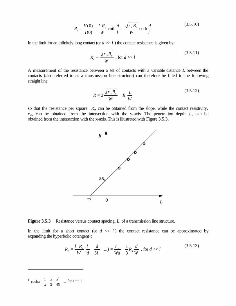
λρ
λλ d
WRd
WR
IV
R scsc cothcoth
)0()0(
=== (3.5.10)
In the limit for an infinitely long contact (or d >> λ) the contact resistance is given by:
W
RR sc
c
ρ= , for d >> λ
(3.5.11)
A measurement of the resistance between a set of contacts with a variable distance L between the contacts (also referred to as a transmission line structure) can therefore be fitted to the following straight line:
WL
RW
RR s
sc +=ρ
2 (3.5.12)
so that the resistance per square, Rs, can be obtained from the slope, while the contact resistivity, ρc, can be obtained from the intersection with the y-axis. The penetration depth, λ, can be obtained from the intersection with the x-axis. This is illustrated with Figure 3.5.3.
0 L −λ
o
o
o
o
RT
2Rc
Figure 3.5.3 Resistance versus contact spacing, L, of a transmission line structure.
In the limit for a short contact (or d << λ) the contact resistance can be approximated by expanding the hyperbolic cotangent1:
Wd
RWd
ddW
RR s
csc 3
1...)
3( +=++=
ρλ
λλ , for d << λ
(3.5.13)
1 ...453
1coth
3
+++=xx
xx for x << 1
The total resistance of a short contact therefore equals the resistance between the contact metal and the semiconductor layer (i.e. the parallel connection of all the resistors, R1, in Figure 3.5.1), plus one third of the end-to-end resistance of the conducting layer underneath the contact metal (i.e the series connection of all resistors, R2, in Figure 3.5.1).

3.6. Metal-Semiconductor Field Effect Transistor (MESFETs) The Metal-Semiconductor-Field-Effect-Transistor (MESFET) consists of a conducting channel positioned between a source and drain contact region as shown in the Figure 3.6.1. The carrier flow from source to drain is controlled by a Schottky metal gate. The control of the channel is obtained by varying the depletion layer width underneath the metal contact which modulates the thickness of the conducting channel and thereby the current between source and drain.
Figure 3.6.1 Structure of a MESFET with gatelength L and channel thickness d.
The key advantage of the MESFET is the higher mobility of the carriers in the channel as compared to the MOSFET. Since the carriers located in the inversion layer of a MOSFET have a wavefunction, which extends into the oxide, their mobility - also referred to as surface mobility - is less than half of the mobility of bulk material. As the depletion region separates the carriers from the surface their mobility is close to that of bulk material. The higher mobility leads to a higher current, transconductance and transit frequency of the device.
The disadvantage of the MESFET structure is the presence of the Schottky metal gate. It limits the forward bias voltage on the gate to the turn-on voltage of the Schottky diode. This turn-on voltage is typically 0.7 V for GaAs Schottky diodes. The threshold voltage therefore must be lower than this turn-on voltage. As a result it is more difficult to fabricate circuits containing a large number of enhancement-mode MESFET.
The higher transit frequency of the MESFET makes it particularly of interest for microwave circuits. While the advantage of the MESFET provides a superior microwave amplifier or circuit, the limitation by the diode turn-on is easily tolerated. Typically depletion-mode devices are used since they provide a larger current and larger transconductance and the circuits contain only a few transistors, so that threshold control is not a limiting factor. The buried channel also yields a better noise performance as trapping and release of carriers into and from surface states and defects is eliminated.
The use of GaAs rather than silicon MESFETs provides two more significant advantages: first of all the room temperature mobility is more than 5 times larger, while the saturation velocity is about twice that in silicon. Second it is possible to fabricate semi-insulating (SI) GaAs substrates,
p-type or semi-insulating substrate
Source
n+
Gate Drain
n+
n-channel depletion region
d
L
p-type or semi-insulating substrate
Source
n+
Gate Drain
n+
n-channel depletion region
d
L
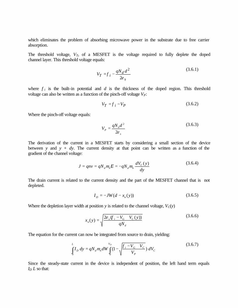
which eliminates the problem of absorbing microwave power in the substrate due to free carrier absorption.
The threshold voltage, VT, of a MESFET is the voltage required to fully deplete the doped channel layer. This threshold voltage equals:
s
diT
dqNV
εφ
2
2−=
(3.6.1)
where φi is the built-in potential and d is the thickness of the doped region. This threshold voltage can also be written as a function of the pinch-off voltage VP:
PiT VV −= φ (3.6.2)
Where the pinch-off voltage equals:
s
dP
dqNV
ε2
2
= (3.6.3)
The derivation of the current in a MESFET starts by considering a small section of the device between y and y + dy. The current density at that point can be written as a function of the gradient of the channel voltage:
dy
ydVqNqNqnvJ C
ndnd
)(µµ −=== E
(3.6.4)
The drain current is related to the current density and the part of the MESFET channel that is not depleted.
))(( yxdJWI nD −−= (3.6.5)
Where the depletion layer width at position y is related to the channel voltage, VC(y)
d
CGisn qN
yVVyx
))((2)(
+−=
φε
(3.6.6)
The equation for the current can now be integrated from source to drain, yielding:
∫∫
+−−=
DV
CP
CGind
L
D dVV
VVdWqNdyI
00
)1(φ
µ (3.6.7)
Since the steady-state current in the device is independent of position, the left hand term equals ID L so that:

( ))(
0
2/3
0
D
D
V
P
CGiVCndD
VVV
VL
WdqNI
+−−=
φµ
(3.6.8)
Two regions:
quadratic region where the depletion layer is less than the channel thickness d
−−
+−−=
P
Gi
P
DGiDdnD
V
V
V
VVV
LW
dNqI2/32/3
32 )()( φφ
µ (3.6.9)
saturated region where the depletion layer at the drain end equals the channel thickness d
TGsatD VVV −=, (3.6.10)
The drain current become independent of the drain voltage and equals:
−−−−=
P
GiPTGdnsatD
V
VVVV
LW
dNqI2/3
32
,)(φ
µ (3.6.11)
Figure 3.6.2 Drain current versus Drain-Source voltage at a gate-source voltage of 0.2, 0.4, 0.6 0.8 and 1.0 Volt for a silicon MESFET with built-in potential of 1 V. Channel parameters and device dimensions are listed in the table below.
Parameter Symbol Value
Channel width W 1 mm
0
1
2
3
4
5
6
7
0 2 4 6
Drain-Source Voltage (V)
Dra
in c
urre
nt (m
A)
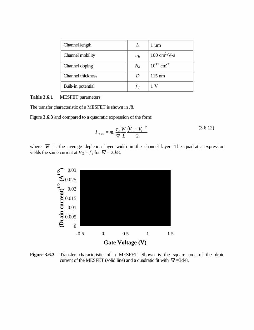
Channel length L 1 µm
Channel mobility µn 100 cm2/V-s
Channel doping Nd 1017 cm-3
Channel thickness D 115 nm
Built-in potential φI 1 V
Table 3.6.1 MESFET parameters
The transfer characteristic of a MESFET is shown in /8.
Figure 3.6.3 and compared to a quadratic expression of the form:
( )2
2
,TGs
nsatDVV
LW
wI
−=
εµ
(3.6.12)
where w is the average depletion layer width in the channel layer. The quadratic expression yields the same current at VG = φi for w = 3d/8.
Figure 3.6.3 Transfer characteristic of a MESFET. Shown is the square root of the drain current of the MESFET (solid line) and a quadratic fit with w =3d/8.
0
0.005
0.01
0.015
0.02
0.025
0.03
-0.5 0 0.5 1 1.5
Gate Voltage (V)
(Dra
in c
urre
nt)1/
2 (A1/
2 )
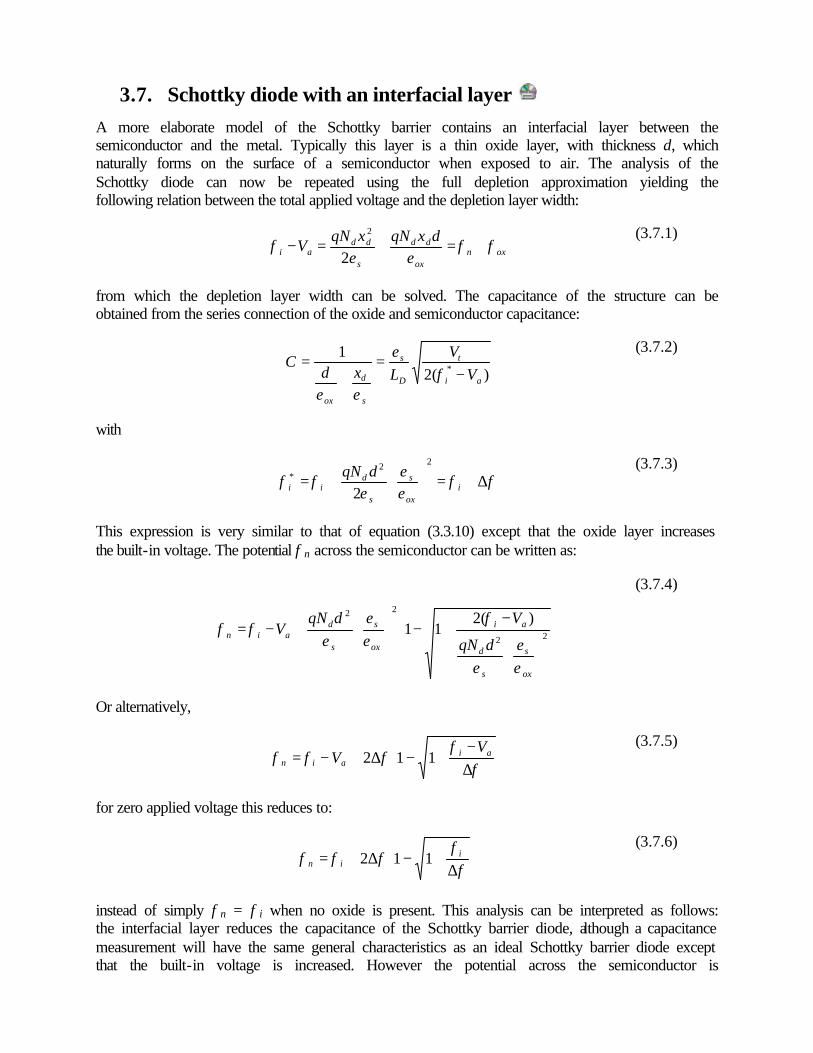
3.7. Schottky diode with an interfacial layer A more elaborate model of the Schottky barrier contains an interfacial layer between the semiconductor and the metal. Typically this layer is a thin oxide layer, with thickness d, which naturally forms on the surface of a semiconductor when exposed to air. The analysis of the Schottky diode can now be repeated using the full depletion approximation yielding the following relation between the total applied voltage and the depletion layer width:
oxn
ox
dd
s
ddai
dxqNxqNV φφ
εεφ +=+=−
2
2
(3.7.1)
from which the depletion layer width can be solved. The capacitance of the structure can be obtained from the series connection of the oxide and semiconductor capacitance:
)(21
*ai
t
D
s
s
d
ox
VV
LxdC
−=
+=
φε
εε
(3.7.2)
with
φφ
εε
εφφ ∆+=
+= i
ox
s
s
dii
dqN22
*
2
(3.7.3)
This expression is very similar to that of equation (3.3.10) except that the oxide layer increases the built-in voltage. The potential φn across the semiconductor can be written as:
−+−
+−= 22
22 )(211
ox
s
s
d
ai
ox
s
s
dain
dqN
VdqNV
εε
ε
φεε
εφφ
(3.7.4)
Or alternatively,
∆−
+−∆+−=φ
φφφφ ai
ainV
V 112 (3.7.5)
for zero applied voltage this reduces to:
∆+−∆+=
φφ
φφφ iin 112
(3.7.6)
instead of simply φn = φi when no oxide is present. This analysis can be interpreted as follows: the interfacial layer reduces the capacitance of the Schottky barrier diode, although a capacitance measurement will have the same general characteristics as an ideal Schottky barrier diode except that the built-in voltage is increased. However the potential across the semiconductor is

decreased due to the voltage drop across the oxide layer, so that at low voltage the barrier for electrons flowing into the semiconductor is reduced yielding a higher current that without the oxide. It has been assumed that the interfacial layer forms a very thin tunnel barrier, which at low voltages does not restrict the current. As the voltage applied to the Schottky barrier is more positive, the depletion layer width reduces, so that the field in the oxide also reduces and with it the voltage drop across the oxide. The current under forward bias conditions therefore approaches that of the ideal Schottky diode until the tunnel barrier restricts the current flow. This results in a higher ideality factor for Schottky barrier with an interfacial layer. From equations (3.7.3) and (3.7.4) we find that the effect is largest for highly doped semiconductors and interfacial layers with low dielectric constant.
The current under forward bias is then given by:
)1(exp* −=
t
as nV
VII
(3.7.7)
with
[ ]t
iss V
IIφφφ ∆+−∆
=/112
exp* (3.7.8)
and
i
nφφ /1
1∆−
= (3.7.9)
An interfacial layer between the metal and semiconductor of a Schottky diode affects the measured barrier height and built-in potential. The total potential within the device is now divided between the interfacial layer and the semiconductor. This causes the potential across the semiconductor to be lower so that carriers can more easily flow from the semiconductor into the metal, yielding a larger current. The interfacial layer also reduces the capacitance.
As an example we consider a thin 3 nm thick oxide layer at the interface of a gold-silicon Schottky diode. The energy band diagram is shown in the Figure 3.7.3.
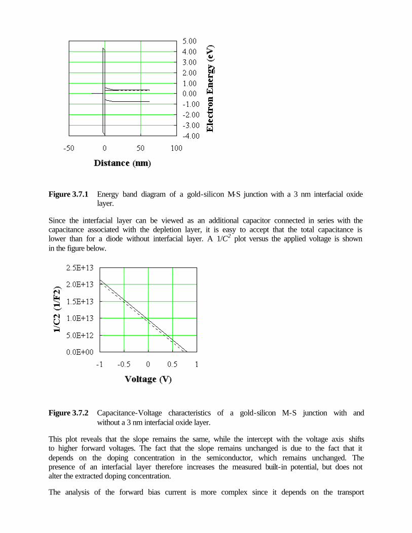
Figure 3.7.1 Energy band diagram of a gold-silicon M-S junction with a 3 nm interfacial oxide layer.
Since the interfacial layer can be viewed as an additional capacitor connected in series with the capacitance associated with the depletion layer, it is easy to accept that the total capacitance is lower than for a diode without interfacial layer. A 1/C2 plot versus the applied voltage is shown in the figure below.
Figure 3.7.2 Capacitance-Voltage characteristics of a gold-silicon M-S junction with and without a 3 nm interfacial oxide layer.
This plot reveals that the slope remains the same, while the intercept with the voltage axis shifts to higher forward voltages. The fact that the slope remains unchanged is due to the fact that it depends on the doping concentration in the semiconductor, which remains unchanged. The presence of an interfacial layer therefore increases the measured built-in potential, but does not alter the extracted doping concentration.
The analysis of the forward bias current is more complex since it depends on the transport

properties of the interfacial layer. However if one assumes that the barrier is so thin that carriers can easily tunnel through, the diode current analysis can be obtained from the standard diffusion analysis, provided that the altered potential across the semiconductor is taken into account.
A comparison of a gold-silicon diode with and without an interfacial layer is shown in the figure below. The figure reveals that the interfacial layer affects both the slope and the intercept of the forward-biased current-voltage when plotted on a semi-logarithmic scale.
Figure 3.7.3 Current-Voltage characteristics of a gold-silicon M-S junction with and without a 3 nm interfacial oxide layer.
In summary, an interfacial layer increases the built-in potential as measured with a C-V measurement, decreases the internal potential across the semiconductor, which increases the measured ideality factor and saturation current. It also decreases the measured barrier height as extracted from the temperature dependence of the saturation current and limits the maximum current density.

3.8. Other Unipolar Junctions
3.8.1. The n-n+ homojunction When contacting semiconductor devices one very often includes highly doped semiconductor layers to lower the contact resistance between the semiconductor and the metal contact. This added layer causes a n-n+ junction within the device. Most often these junctions are ignored in the analysis of devices, in part because of the difficulty treating them correctly, in part because they can simply be ignored. The build-in voltage of a n-n+ junction is given by:
d
dtFnFni N
NVEE
q
+=−= + ln)(
1φ
(3.8.1)
Which means that the built-in voltage is about 59.4 meV if the doping concentrations differ by a factor 10. It is because of this small built-in voltage that this junction is often ignored. However large ratios in doping concentration do cause significant potential variations.
The influence of the n-n+ junction must be evaluated in conjunction with its current voltage characteristics: if the n-n+ junction is in series with a p-n diode, the issue is whether or not the n-n+ junction affects the operation of the p-n junction in any way. At low current densities one can expect the p-n diode to dominate the current flow, whereas at high current densities the n-n+ junction could play a role if not designed properly.
For the analysis of the n-n+ junction we start from a flat band energy band diagram connecting the two regions in absence of an electric field. One can visualize that electrons will flow from the n+ region and accumulate in the n-type region. However, since the carrier concentration must be continuous (this is only required in a homojunction), the carrier density in the n region is smaller that the doping concentration of the n+ region, and the n+ region is not completely depleted. The full depletion approximation is therefore not applicable. Instead one recognizes the situation to be similar to that of a metal-semiconductor junction: the n+ is depleted but has a small voltage across the semiconductor as in a Schottky barrier with small voltage applied, whereas the n region is accumulated as in an ohmic contact. A general solution of this structure requires the use of equation [3.1.4].
A simple solution is obtained in the limit where the potential across both regions is smaller than the thermal voltage. The charge in the n-n+ structure region is then given by:
DnDnDn
ai
Dn
snL
xLLV
Lx exp)(
++−
−=φε
ρ for x < 0 (3.8.2)
+++
+ −+−
−=DnDnDn
ai
Dn
snL
xLLV
Lx exp)(
φερ for x > 0
(3.8.3)
where the interface is assumed at x equal zero, and LD,n and LD,n+ are the extrinsic Debye lengths in the material. Applying Poisson's equation one finds the potentials to be:

DnDnDn
aiDnn L
xLLV
Lx exp)(++
−=
φφ for x < 0
(3.8.4)
++++
−+−
=DnDnDn
aiDnn L
xLLV
Lx exp)(φ
φ for x < 0 (3.8.5)
The solutions for the charge density, electric field, potential and energy band diagram are plotted in the Figure 3.8.1:
Distance [nm]
Cha
rge
Den
sity
[C/c
m2]
-0.004
-0.002
0
0.002
0.004
0.006
0.008
0.01
-200 -150 -100 -50 0 50 100
DistanceE
lect
ric
Fie
ld [V
/cm
]
-12000
-10000
-8000
-6000
-4000
-2000
0-200 -150 -100 -50 0 50 100

Distance [nm]
Pot
enti
al [V
]
0
0.01
0.02
0.03
0.04
0.05
0.06
-200 -150 -100 -50 0 50 100
Distance [nm]
Ene
rgy
[eV
]
-1
-0.8
-0.6
-0.4
-0.2
0
0.2
0.4
-200 -150 -100 -50 0 50 100
Ec
Ev
Ei
Figure 3.8.1 Charge, electric field, potential and energy banddiagram in a silicon n-n+ structure
with Nd = 1016 cm-3, Nd+ = 1017 cm-3 and Va = 0.

3.8.2. The n-n+ heterojunction Consider a n-n+ heterojunction including a spacer layer with thickness d as shown in Figure 3.8.2
.
cn
vn
vn
fncn
∆E
∆E
fn
+
EE
E
EE
E
c
v
++
-d 0
x
spacerlayer
n -layer n-layer
qφ i
+
Figure 3.8.2 Flatband energy diagram of a n-n+ heterojunction with a spacer layer with thickness d.
The built-in voltage for a n-n+ heterojunction with doping concentrations Nd and Nd+ is given by:
c
ncd
ncdtFnFni E
NN
NNVEE
q∆+=−=
+
++
,
,ln)(
1φ
(3.8.6)
Where Nc,n and Nc,n+ are the effective densities of states of the low and high-doped region
respectively. Unlike a homojunction, the heterojunction can have a built-in voltage, which is substantially larger than the thermal voltage. This justifies using the full depletion approximation for the depleted region. For the accumulated region one has to consider the influence of quantization of energy levels because of the confinement of carriers by the electric field and the hetero-interface.
3.8.2.1.Analysis without quantization
For the classic case where the material does not become degenerate at the interface one can use [3.1.4b] to find the total charge in the accumulation layer:
]1[exp2, −−==− ++
t
n
t
n
D
tnsndacc VVL
VxqNQ
φφε
(3.8.7)
while the potentials and the field can be solved for a given applied voltage using:
ainspn V−=+++ φφφφ (3.8.8)

+++ =
dns
nnsn Nq
E
,
22,
2 ε
εφ
(3.8.9)
sps
nsnsp
dE
,εε
φ = (3.8.10)
The subscript sp refers to the undoped spacer layer with thickness d, which is located between the two doped regions. These equations can be solved by starting with a certain value of φn, which enables to calculate the electric field, the other potentials and the corresponding applied voltage, Va.
3.8.2.2.Analysis including quantization
The analysis of a n-n+ heterojunction including quantized levels is more complicated because the energy levels depend on the potential which can only be calculated if the energy levels are known. A self-consistent calculation is therefore required to obtain a correct solution. An approximate method, which also clarifies the steps needed for a correct solution is described below1.
Starting from a certain density of electrons per unit area, Ns, which are present in the accumulation layer, one finds the field at the interface:
ns
sn
qNE
,ε=
(3.8.11)
We assume that only the n = 1 energy level is populated with electrons. The minimal energy can be expressed as a function of the electric field using equation2 [A.1.17]:
3/23/1
*
2
1 )8
9()
2( nn qE
mE
πh=
(3.8.12)
The bandgap discontinuity ∆Ec can then be related to the other potentials of the junction using [3.2.4], [3.2.6] and [A.1.8], yielding:
spn
d
nc
qwc
nnsnac qq
N
NkT
qN
EkTEqVE φφ
ε+++−+=−∆ +
+
+,
,
,1 ln]1)ln[exp(
(3.8.13)
where the potentials, φn+ and φsp, in turn can be expressed as a function of En:
1A similar analysis can also be found in Weisbuch and Vinter, Quantum Semiconductor Structures, pp 40-41, Academic Press, 1991.
2A more detailed quantum mechanical derivation yields the 9π/8 term instead of 3π/2. See for instance F. Stern, Phys. Rev. B 5 p 4891, (1972). The two differ by (3/4)3/2=0.826 or 17.5%

+++ =
dns
nnsn Nq
E
,
22,
2 ε
εφ
(3.8.14)
sps
nnssp
dE
,
,
ε
εφ =
(3.8.15)
These equations can be combined into one transcendental equation as a function of the electric field, En.
dns
nns
d
nc
qwc
nnsnac N
E
N
NkT
qN
EkTEqVE
,
22,,
,
,1 2
ln]1)ln[exp(ε
εε++−+=−∆
+++
+
(3.8.16)
Once En is known all potentials can be obtained.
Distance [cm]
Ene
rgy
[eV
]
-0.3-0.25-0.2
-0.15-0.1
-0.050
0.050.1
0.15
-0.00001 -0.000005 0 0.000005 0.00001
Efn+
Efn
Ec
Figure 3.8.3 Energy banddiagram of a Al0.4Ga0.6As/GaAs n+-n heterostructure with Nd
+ = 1017 cm-3, Nd = 1016 cm-3, d = 10 nm and Va = 0.15 V. Comparison of analysis without quantization (upper curve) to that with quantization (lower curve)
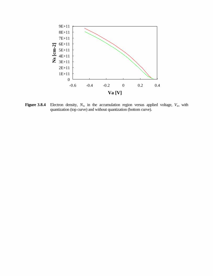
Va [V]
Ns
[cm
-2]
01E+112E+113E+114E+115E+116E+117E+118E+119E+11
-0.6 -0.4 -0.2 0 0.2 0.4
Figure 3.8.4 Electron density, Ns, in the accumulation region versus applied voltage, Va, with
quantization (top curve) and without quantization (bottom curve).

3.8.3. Currents across a n+-n heterojunction Current transport across a n+-n heterojunction is similar to that of a metal-semiconductor junction: Diffusion, thermionic emission as well as tunneling of carriers across the barrier can occur. However to identify the current components one must first identify the potentials φn
+ and φn by solving the electrostatic problem. From the band diagram one finds that a barrier exists for electrons going from the n+ to the n-doped region as well as for electrons going in the opposite direction.
The analysis in the first section discusses the thermionic emission and yields a closed form expression based on a set of specific assumptions. The derivation also illustrates how a more general expression could be obtained. The next section describes the current-voltage characteristics of carriers traversing a depletion region, while the last section discusses how both effects can be combined.
3.8.3.1.Thermionic emission current across a n+-n heterojunction
The total current due to thermionic emission across the barrier is given by the difference of the current flowing from left to right and the current flowing from right to left. Rather than re-deriving the expression for thermionic emission, we will apply equation [3.1.40] to the n+-n heterojunction. One complication arises from the fact that the effective mass of the carriers is different on each side of the hetero-junction which would seem to indicate that the Richardson constant is different for carrier flow from left to right compared to the flow from right to left. A more detailed analysis reveals that the difference in effective mass causes a quantum mechanical reflection at the interface, causing carriers with the higher effective mass to be reflected back while carriers with the smaller effective mass are to first order unaffected3. We therefore use equation [3.1.40] for flow in both directions while using the Richardson constant corresponding to the smaller of the two effective masses, yielding:
)0(exp[
)0(exp[ ,,2*
kT
ExE
kT
qExETAJ FcnnFc
HJ−=
−−+−=
−=++ φ
(3.8.17)
where the potentials are related to the applied voltage by4:
ainn V−=++ φφφ (3.8.18)
and the built-in voltage is given by:
q
ExEExEE FncFncci
))(())(( −∞=+−−∞=−∆=
+φ
(3.8.19)
Combining these relations yields:
3A.A. Grinberg, "Thermionic emission in heterojunction systems with different effective electronic masses," Phys. Rev. B, pp. 7256-7258, 1986
4No spacer layer is assumed in this derivation, but could easily be added if desired.

]1][expexp[]exp[
*2* −−=
t
a
t
B
t
nHJ V
VVV
TAJφφ
(3.8.20)
where the barrier height φB* is defined as:
qExEE Fncc
B))((* −∞=∆
=φ (3.8.21)
Assuming full depletion in the n+ depletion region and using equation [3.1.10] for the accumulated region, the charge balance between the depletion and accumulation layer takes the following form:
]1[exp22 ,, −−=+++
t
n
t
nnsndns VV
qNφφ
εφε (3.8.22)
Combining equations [3.2.20] with [3.2.16] yields a solution for φn+ and φn.
For the special case where εsn+Nd
+ = εsnNd and φn>>Vt these equations reduce to:
t
ntnnai V
VVφ
φφφ exp=+=− + (3.8.23)
The current (given by [3.2.18]) can then be expressed as a function of the applied voltage Va
]1)[expexp()1(
**−−−=
t
a
t
B
i
aiHJ V
VV
VkTqA
Jφ
φφ
(3.8.24)
Whereas this expression is similar to that of a metal-semiconductor barrier, it differs in that the temperature dependence is somewhat modified and the reverse bias current increases almost linearly with voltage. Under reverse bias the junction can be characterized as a constant resistance, RHJ, which equals:
)exp(
2*
t
B
ta
HJHJ VV
TAAV
AJR
φ−==
(3.8.25)
where A is the area of the junction. This shows that the resistance changes exponentially with the barrier height. Grading of the heterojunction is typically used to reduce the spike in the energy band diagram and with it the resistance across the interface.
3.8.3.2.Calculation of the Current and quasi-Fermi level throughout a Depletion Region
We typically assume the quasi-Fermi level to be constant throughout the depletion region. This assumption can be justified for a homojunction but is not necessarily correct for a heterojunction p-n diode.

For a homojunction p-n diode we derived the following expression for the minority carrier density in the quasi-neutral region of a "long" diode
)exp()1(exp00
nt
app L
xVV
nnnn −−=−≅ (3.8.26)
so that the maximum change in the quasi-Fermi level, which occurs at the edge of the depletion region, equals:
n
inLkT
dxnn
kTd
dxdF
≅=)ln(
(3.8.27)
so that the change of the quasi-Fermi level can be ignored if the depletion region width is smaller than the diffusion length as is typically the case in silicon p-n diodes.
For a hetero-junction p-n diode one can not assume that the quasi-Fermi level is continuous, especially when the minority carriers enter a narrow bandgap region in which the recombination rate is so high that the current is limited by the drift/diffusion current in the depletion region located in the wide bandgap semiconductor.
The current density can be calculated from:
dxdn
qDnEqJ nnn += µ (3.8.28)
Assuming the field to be constant throughout the depletion region one finds for a constant current density the following expression for the carrier density at the interface:
)exp(
t
nd
n VEx
NEq
Jn −+=
µ
(3.8.29)
While for zero current one finds, for an arbitrary field
)exp()
)(exp(
0
t
nd
td V
NV
dxxENn
φ−=−= ∫
∞−
(3.8.30)
Combining the two expressions we postulate the following expression for the carrier density:
)exp(
max t
nd
n VN
EqJ
nφ
µ−+=
(3.8.31)
The carrier density can also be expressed as a function of the total change in the quasi-Fermi level across the depletion region, ∆Efn;
)exp()exp( ,
t
nF
t
nd V
E
VNn
∆−−=
φ
(3.8.32)

which yields the following expressions for the current density due to drift/diffusion:
)1))(exp(exp( ,
max −∆
−−−=kT
E
VNEqJ nF
t
ndn
φµ
(3.8.33)
where is max the field at the heterojunction interface. If ∆Efn equals the applied voltage, as is the case for an n+- n heterostructure, this expression equals:
)1))(exp(exp(max −−−=
t
a
t
ndn V
VV
NEqJφ
µ (3.8.34)
which reduces for a MS junction to:
R
nthermionicdd v
EJJ maxµ
= (3.8.35)
so that thermionic emission dominates for vR << µn max or when the drift velocity is larger than the Richardson velocity.5
3.8.3.3.Calculation of the current due to thermionic emission and drift/diffusion
The calculation of the current through a n+-n junction due to thermionic emission and drift/diffusion becomes straightforward once one realizes that the total applied voltage equals the sum of the quasi-Fermi level variation, ∆Efn, across each region. For this analysis we therefore rewrite the current expressions as a function of ∆Efn, while applying the expression for the
drift/diffusion current to the n+ material.
]1)[expexp()exp( 1,
*2* −
∆−=
kT
E
VVTAJ nF
t
B
t
nthermionic
φφ
(3.8.36)
]1)[expexp( 2,
*
,max/ −∆
−−= ++kT
E
VNEqJ nF
t
Bncndiffusiondrift
φµ
(3.8.37)
5It should be noted here that the drift/diffusion model is not valid anymore as the drift velocity of the carriers approaches the thermal velocity.
3.9. Currents through insulators Current mechanisms through materials, which do not contain free carriers can be distinctly different from those in doped semiconductors or metals. The following section discusses Fowler-Nordheim Tunneling, Poole-Frenkel emission, Space charge effects as well as Ballistic transport
3.9.1. Fowler-Nordheim tunneling
Fowler-Nordheim tunneling has been studied extensively in Metal-Oxide-Semiconductor structures where it has been shown to be the dominant current mechanism, especially for thick oxides. The basic idea is that quantum mechanical tunneling from the adjacent conductor into the insulator limits the current through the structure. Once the carriers have tunneled into the insulator they are free to move within the valence or conduction band of the insulator. The calculation of the current is based on the WKB approximation (as derived section 3.4.4) yielding the following relation between the current density, JFN, and the electric field in the oxide, Eox:
)
)(2
34
(exp2/3*
2
ox
BoxoxoxFNFN
mCJ
EE φ
h−=
(3.9.1)
where φB is the barrier height at the conductor/insulator interface in Volt, as shown in the figure below for electron tunneling from highly1 n-type doped silicon into the silicon dioxide.
To check for this current mechanism, experimental I-V characteristics are typically plotted as ln(JFN//Eox 2) versus 1/Eox, a so-called Fowler-Nordheim plot. Provided the effective mass of the insulator is known (for SiO2, mox
* = 0.42 m0) one can then fit the experimental data to a straight line yielding a value for the barrier height.
It is this type of measurement which has yielded experimental values for the conduction band difference between silicon and silicon-dioxide. The same method could also be used to determine heterojunction energy band off-sets provided Fowler-Nordheim tunneling is indeed the dominant current mechanism2. It is important to stress that carriers must tunnel through the insulator, which requires:
Boxd φ≥E (3.9.2)
which is typically the case for thick oxides and high electric fields.
3.9.2. Poole-Frenkel emission
The expression for Fowler-Nordheim tunneling implies that carriers are free to move through the insulator. Whereas this is indeed the case in thermally grown silicon-dioxide it is frequently not so in deposited insulators which contain a high density of structural defects. Silicon nitride (Si3N4) is an example of such material. The structural defects cause additional energy states close to the bandedge called traps. These traps restrict the current flow because of a capture and
1This condition is added to eliminate additional complexity caused by bandbending at the interface.
2This condition would required very large energy band discontinuities.

emission process, thereby becoming the dominant current mechanism. The current is a simple drift current described by
NqnJ Eµ= (3.9.3)
while the carrier density depends exponentially on the depth of the trap which is corrected for the electric field3.
)](exp[0
N
NB
qkTq
nnπε
φE
−−= (3.9.4)
The total current then equals:
)](exp[0
N
NBNPF
qkTq
qnJπε
φµE
E −−= (3.9.5)
The existence of a large density of shallow4 traps in CVD silicon nitride makes Poole-Frenkel emission5 a frequently observed and well-characterized mechanism.
3.9.3. Space charge limited current
Both Fowler-Nordheim tunneling and Poole-Frenkel emission mechanism yield very low current densities with correspondingly low carrier densities. For structures where carriers can readily enter the insulator and freely flow through the insulator one finds that the resulting current and carrier densities are much higher. The density of free carriers causes a field gradient, which limits the current density. This situation occurs in lowly doped semiconductors and vacuum tubes. Starting from an expression for the drift current and Gauss's law (where we assume that the insulator contains no free carriers if no current flows)
EµqpJ = (3.9.6)
εqp
dxd
=E
(3.9.7)
we can eliminate the carrier density, p, yielding:
3This correction is equivalent to the Schottky barrier lowering due to the presence of an electric field.
4deep traps also exist in silicon nitride. While these easily capture carriers, they are too deep to allow emission even in the presence of large fields. This causes a fixed charge in the silicon nitride which remains when the applied bias is removed. This charge trapping mechanism is used in non-volatile MNOS memory devices.
5J. Frenkel, "On Pre-Breakdown Phenomena in insulators and Electronic Semiconductors," Phys. Rev., Vo l 54, p 647, 1938.

dxdJ EE=
εµ
(3.9.8)
Integrating this expression from 0 to x, where we assume the electric field to be zero6 at x = 0 one obtains:
2
2E=
εµJx
or εµxJ
x2
)( =E (3.9.9)
integrating once again from x = 0 to x = d with V(0) = V and V(d) = 0, one finds:
2/32 2/3
0
dJdxV
d
εµ== ∫E
(3.9.10)
from which one obtains the expression for the space-charge-limited current:
3
2
89
dV
Jµε
= (3.9.11)
3.9.4. Ballistic Transport in insulators
Ballistic transport is carrier transport without scattering or any other mechanism, which would cause a loss of energy. Combining energy conservation, current continuity and Gauss's law one finds the following current-voltage relation:
2
2/3
*2
94
d
V
m
qJ
ε=
(3.9.12)
where d is the thickness of the insulator and m* is the effective mass of the carriers.
6This implies an infinite carrier density. The analysis can be modified to allow for a finite carrier density. However the carrier pile-up do to the current restriction typically provides a very high carrier density at x=0.

example 3
Title Page Table of Contents Help Copyright B. Van Zeghbroeck, 2004
Chapter 3: Metal-Semicond. Junctions
Examples
Example 3.1 Consider a chrome-silicon metal-semiconductor junction with Nd = 1017 cm-3. Calculate the barrier height and the built-in potential. Repeat for a p-type semiconductor with the same doping density.
Example 3.2 Consider a chrome-silicon metal-semiconductor junction with Nd = 1017 cm-3. Calculate the depletion layer width, the electric field in the silicon at the metal-semiconductor interface, the potential across the semiconductor and the capacitance per unit area for an applied voltage of -5 V.
http://ece-www.colorado.edu/~bart/book/book/chapter3/ch3_ex.htm11/10/2004 16:40:24
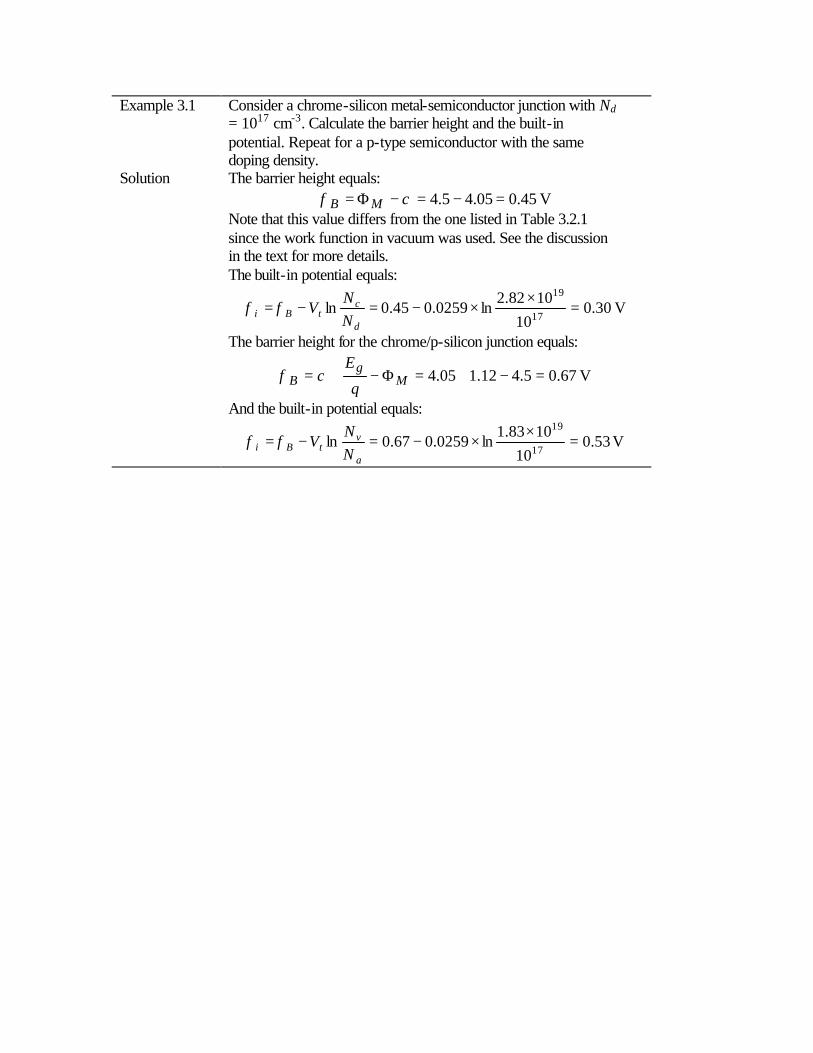
Example 3.1 Consider a chrome-silicon metal-semiconductor junction with Nd = 1017 cm-3. Calculate the barrier height and the built-in potential. Repeat for a p-type semiconductor with the same doping density.
Solution The barrier height equals: V 45.005.45.4 =−=−Φ= χφ MB
Note that this value differs from the one listed in Table 3.2.1 since the work function in vacuum was used. See the discussion in the text for more details. The built-in potential equals:
V 30.010
1082.2ln0259.045.0ln
17
19
=×
×−=−=d
ctBi N
NVφφ
The barrier height for the chrome/p-silicon junction equals:
V 67.05.412.105.4 =−+=Φ−+= Mg
B q
Eχφ
And the built-in potential equals:
V 53.010
1083.1ln0259.067.0ln
17
19
=×
×−=−=a
vtBi N
NVφφ

Example 3.2 Consider a chrome-silicon metal-semiconductor junction with Nd = 1017 cm-3. Calculate the depletion layer width, the electric field in the silicon at the metal-semiconductor interface, the potential across the semiconductor and the capacitance per unit area for an applied voltage of -5 V.
Solution The depletion layer width equals:
m 26.010106.1
)53.0(1085.89.112
)(2
1719
14µ
φε
=××
+××××=
−=
−
−
d
aisd qN
Vx
where the built-in potential was already calculated in Example 3.1. The electric field in the semiconductor at the interface is:
V/cm 100.41085.89.11
106.210106.1
)0(
514
51719×=
××
××××=
==
−
−−s
dd xqNx
εE
The potential equals:
V 3.52
)(2
=−=== ais
ddd V
xqNxx φ
εφ
And the capacitance per unit area is obtained from:
25
14nF/cm 40
106.2
1085.89.11 =
×
××==
−
−
d
sj x
Cε

http://ece-www.colorado.edu/~bart/book/book/chapter3/ch3_p.htm
Title Page Table of Contents Help Copyright B. Van Zeghbroeck, 2004
Chapter 3: Metal-Semicond. Junctions
Problems
1. Consider a gold-GaAs Schottky diode with a capacitance of 1 pF at -1 V. What is the doping density of the GaAs? Also calculate the depletion layer width at zero bias and the field at the surface of the semiconductor at -10 V. The area of the diode is 10-5 cm2.
2. Consider two Schottky diodes with built-in potential φi = 0.6 V. The diodes are connected in series and reversed biased. The diodes are identical except that the area of one is four times larger than that of the other one. Calculate the voltage at the middle node, Vout, as a function of the applied voltage, Vin. Assume there is no dc current going through either diode so that the charge at the middle node is independent of the applied voltage.
3. Using the work functions listed in table 3.2.1, predict which metal-semiconductor junctions are expected to be ohmic contacts. Use the ideal interface model.
4. Design a platinum-silicon diode with a capacitance of 1 pF and a maximum electric field less than 104 V/cm at -10 V bias. Provide a possible doping density and area. Make sure the diode has an area between 10-5 and 10-7 cm2. Is it possible to satisfy all requirements if the doping density equals 1017 cm-3?
5. A platinum-silicon diode (area = 10-4 cm-3, Nd = 1017 cm-3) is part of an LC tuning circuit containing a 100 nH inductance. The applied voltage must be less than 5 V. What is the tuning range of the circuit? The resonant frequency equals
, where L is the inductance and C is the diode capacitance.
http://ece-www.colorado.edu/~bart/book/book/chapter3/ch3_p.htm11/10/2004 16:40:44

http://ece-www.colorado.edu/~bart/book/book/chapter3/ch3_r.htm
Title Page Table of Contents Help Copyright B. Van Zeghbroeck, 2004
Chapter 3: Metal-Semicond. Junctions
Review Questions
1. What is a flatband diagram?
2. Define the barrier height of a metal-semiconductor junction. Can the barrier height be negative? Explain.
3. Define the built-in potential. Also provide an equation and state the implicit assumption(s).
4. Name three possible reasons why a measured barrier height can differ from the value calculated using equations (3.2.1) or (3.2.2).
5. How does the energy band diagram of a metal-semiconductor junction change under forward and reverse bias? How does the depletion layer width change with bias?
6. What is the full depletion approximation? Why do we need the full depletion approximation?
7. What mechanism(s) cause(s) current in a metal-semiconductor junction?
http://ece-www.colorado.edu/~bart/book/book/chapter3/ch3_r.htm11/10/2004 16:41:09

Chapter 3 Bibliography
Title Page Table of Contents Help Copyright B. Van Zeghbroeck, 2004
Chapter 3: Metal-Semicond. Junctions
Bibliography
1. Physics of Semiconductor Devices, Second edition, S. M. Sze, Wiley & Sons, 1981, Chapter 5.
2. Device Electronics for Integrated Circuits, Second edition, R.S. Muller and T. I. Kamins, Wiley & Sons, 1986, Chapter 3.
http://ece-www.colorado.edu/~bart/book/book/chapter3/ch3_b.htm11/10/2004 16:41:19

http://ece-www.colorado.edu/~bart/book/book/chapter3/ch3_g.htm
Title Page Table of Contents Help Copyright B. Van Zeghbroeck, 2004
Chapter 3: Glossary
Name
Applied bias Voltage applied to the structure Flatband diagram Energy band diagram of a M-S junction containing no net charge
Richardson constant Material constant which affects the thermionic emission current in a metal-semiconductor junction
Richardson velocity Average thermal velocity of carriers moving in a specific direction
Schottky barrier Barrier between a metal and semiconductor as seen by an electron or hole at the Fermi energy in the metal
Schottky barrier lowering Lowering of the Schottky barrier height due to image forces (only used in current calculations)
http://ece-www.colorado.edu/~bart/book/book/chapter3/ch3_g.htm11/10/2004 16:41:27

Chapter 3 Equations
Title Page Table of Contents Help Copyright B. Van Zeghbroeck, 2004
Chapter 3: Metal-Semicond. Junctions
Equations
(3.2.1)
(3.2.2)
(3.2.3)
(3.2.4)
(3.2.5)
(3.3.1)
(3.3.2)
(3.3.3)
http://ece-www.colorado.edu/~bart/book/book/chapter3/ch3_eq.htm (1 of 3)11/10/2004 16:41:35

Chapter 3 Equations
(3.3.4)
(3.3.5)
(3.3.6)
(3.3.7)
(3.3.8)
(3.3.9)
(3.3.10)
(3.3.11)
(3.4.1)
(3.4.2)
http://ece-www.colorado.edu/~bart/book/book/chapter3/ch3_eq.htm (2 of 3)11/10/2004 16:41:35

Chapter 3 Equations
(3.4.3)
(3.4.4)
(3.4.5)
(3.4.6)
(3.4.7)
(3.4.8)
(3.4.9)
(3.4.10)
http://ece-www.colorado.edu/~bart/book/book/chapter3/ch3_eq.htm (3 of 3)11/10/2004 16:41:35
Schottky diode current
Title Page Table of Contents Help Copyright B. Van Zeghbroeck, 2004
Chapter 3: Metal-Semicond. Junctions
3.9. Currents through insulators Note:This is a temporary file, which is to be replaced with a fully hyperlinked HTML file. Meanwhile, the text can be accessed by clicking on the PDF icon.
http://ece-www.colorado.edu/~bart/book/book/chapter3/ch3_9.htm11/10/2004 16:48:20

p-n Junctions
Title Page Table of Contents Help Copyright B. Van Zeghbroeck, 2004
Chapter 4: p-n Junctions
4.1. Introduction
P-n junctions consist of two semiconductor regions of opposite type. Such junctions show a pronounced rectifying behavior. They are also called p-n diodes.The p-n junction is a versatile element, which can be used as a rectifier, as an isolation structure and as a voltage-dependent capacitor. In addition, they can be used as solar cells, photodiodes, light emitting diodes and even laser diodes. They are also an essential part of Metal-Oxide-Silicon Field-Effects-Transistors (MOSFETs) and Bipolar Junction Transistors (BJTs).
http://ece-www.colorado.edu/~bart/book/book/chapter4/ch4_1.htm11/10/2004 16:48:54

p-n Junctions
Title Page Table of Contents Help Copyright B. Van Zeghbroeck, 2004
Chapter 4: p-n Junctions
4.2. Structure and principle of operation4.2.1. Structure4.2.2. Thermal equilibrium4.2.3. The built-in potential4.2.4. Forward and reverse bias
A p-n junction consists of two semiconductor regions with opposite doping type as shown in Figure 4.2.1. The region on the left is p-type with an acceptor density Na, while the region on the right is n-type with a donor density Nd. The dopants are assumed to be shallow, so that the electron (hole) density in the n-type (p-type) region is approximately equal to the donor (acceptor) density.
Figure 4.2.1 : Cross-section of a p-n junctionWe will assume, unless stated otherwise, that the doped regions are uniformly doped and that the transition between the two regions is abrupt. We will refer to this structure as being an abrupt p-n junction. Frequently we will deal with p-n junctions in which one side is distinctly higher-doped than the other. We will find that in such a case only the low-doped region needs to be considered, since it primarily determines the device characteristics. We will refer to such a structure as a one-sided abrupt p-n junction. The junction is biased with a voltage Va as shown in Figure 4.2.1. We will call the junction forward-biased if a positive voltage is applied to the p-doped region and reversed-biased if a negative voltage is applied to the p-doped region. The contact to the p-type region is also called the anode, while the contact to the n-type region is called the cathode, in reference to the anions or positive carriers and cations or negative carriers in each of these regions.
http://ece-www.colorado.edu/~bart/book/book/chapter4/ch4_2.htm (1 of 5)11/10/2004 16:49:04

p-n Junctions
4.2.1. Flatband diagram
The principle of operation will be explained using a gedanken experiment, an experiment, which is in principle possible but not necessarily executable in practice. We imagine that one can bring both semiconductor regions together, aligning both the conduction and valence band energies of each region. This yields the so-called flatband diagram shown in Figure 4.2.2.
Figure 4.2.2 : Energy band diagram of a p-n junction (a) before and (b) after merging the n-type and p-type regions
Note that this does not automatically align the Fermi energies, EFn and EFp. Also, note that this flatband diagram is not an equilibrium diagram since both electrons and holes can lower their energy by crossing the junction. A motion of electrons and holes is therefore expected before thermal equilibrium is obtained. The diagram shown in Figure 4.2.2 (b) is called a flatband diagram. This name refers to the horizontal band edges. It also implies that there is no field in the semiconductor and no charge.
4.2.2. Thermal equilibrium
To reach thermal equilibrium, electrons/holes close to the metallurgical junction diffuse across the junction into the p-type/n-type region where hardly any electrons/holes are present. This process leaves the ionized donors (acceptors) behind, creating a region around the junction, which is depleted of mobile carriers. We call this region the depletion region, extending from x = -xp to x = xn. The charge due to the ionized donors and acceptors causes an electric field, which in turn causes a drift of carriers in the opposite direction. The diffusion of carriers continues until the drift current balances the diffusion current, thereby reaching thermal equilibrium as indicated by a constant Fermi energy. This situation is shown in Figure 4.2.3:
http://ece-www.colorado.edu/~bart/book/book/chapter4/ch4_2.htm (2 of 5)11/10/2004 16:49:04
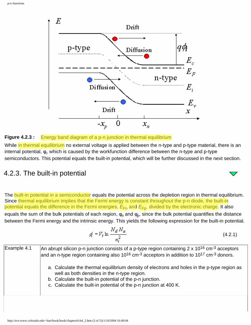
p-n Junctions
Figure 4.2.3 : Energy band diagram of a p-n junction in thermal equilibriumWhile in thermal equilibrium no external voltage is applied between the n-type and p-type material, there is an internal potential, φi, which is caused by the workfunction difference between the n-type and p-type semiconductors. This potential equals the built-in potential, which will be further discussed in the next section.
4.2.3. The built-in potential
The built-in potential in a semiconductor equals the potential across the depletion region in thermal equilibrium. Since thermal equilibrium implies that the Fermi energy is constant throughout the p-n diode, the built-in potential equals the difference in the Fermi energies, EFn and EFp, divided by the electronic charge. It also equals the sum of the bulk potentials of each region, φn and φp, since the bulk potential quantifies the distance between the Fermi energy and the intrinsic energy. This yields the following expression for the built-in potential.
(4.2.1)
Example 4.1 An abrupt silicon p-n junction consists of a p-type region containing 2 x 1016 cm-3 acceptors and an n-type region containing also 1016 cm-3 acceptors in addition to 1017 cm-3 donors.
a. Calculate the thermal equilibrium density of electrons and holes in the p-type region as well as both densities in the n-type region.
b. Calculate the built-in potential of the p-n junction.c. Calculate the built-in potential of the p-n junction at 400 K.
http://ece-www.colorado.edu/~bart/book/book/chapter4/ch4_2.htm (3 of 5)11/10/2004 16:49:04

p-n Junctions
Solution a. The thermal equilibrium densities are:In the p-type region:
p = Na = 2 x 1016 cm-3
n = ni2/p = 1020/2 x 1016 = 5 x 103 cm-3
In the n-type regionn = Nd - Na = 9 x 1016 cm-3
p = ni2/n = 1020/(1 x 1016) = 1.11 x 103 cm-3
b. The built-in potential is obtained from:
c. Similarly, the built-in potential at 400 K equals:
where the instrinsic carrier density at 400 K was obtained from example 2.4.b
4.2.4. Forward and reverse bias
We now consider a p-n diode with an applied bias voltage, Va. A forward bias corresponds to applying a positive voltage to the anode (p-type region) relative to the cathode (n-type region). A reverse bias corresponds to a negative voltage applied to the cathode. Both bias modes are illustrated with Figure 4.2.4. The applied voltage is proportional to the difference between the Fermi energy in the n-type and p-type quasi-neutral regions. As a negative voltage is applied, the potential across the semiconductor increases and so does the depletion layer width. As a positive voltage is applied, the potential across the semiconductor decreases and with it the depletion layer width. The total potential across the semiconductor equals the built-in potential minus the applied voltage, or:
(4.2.1)
http://ece-www.colorado.edu/~bart/book/book/chapter4/ch4_2.htm (4 of 5)11/10/2004 16:49:04

p-n Junctions
Figure 4.2.4: Energy band diagram of a p-n junction under reverse and forward bias
http://ece-www.colorado.edu/~bart/book/book/chapter4/ch4_2.htm (5 of 5)11/10/2004 16:49:04
Electrostatic analysis of a p-n diode
Title Page Table of Contents Help Copyright B. Van Zeghbroeck, 2004
Chapter 4: p-n Junctions
4.3. Electrostatic analysis of a p-n diode4.3.1. General discussion - Poisson's equation4.3.2. The full-depletion approximation4.3.3. Full depletion analysis4.3.4. Junction capacitance
The electrostatic analysis of a p-n diode is of interest since it provides knowledge about the charge density and the electric field in the depletion region. It is also required to obtain the capacitance-voltage characteristics of the diode. The analysis is very similar to that of a metal-semiconductor junction (section 3.3). A key difference is that a p-n diode contains two depletion regions of opposite type.
4.3.1. General discussion - Poisson's equation
The general analysis starts by setting up Poisson's equation:
(4.3.1)
where the charge density, ρ, is written as a function of the electron density, the hole density and the donor and acceptor densities. To solve the equation, we have to express the electron and hole density, n and p, as a function of the potential, φ, yielding:
(4.3.2)
with
(4.3.3)
where the potential is chosen to be zero in the n-type region, far away from the p-n interface.This second-order non-linear differential equation (4.3.2) can not be solved analytically. Instead we will make the simplifying assumption that the depletion region is fully depleted and that the adjacent neutral regions contain no charge. This full depletion approximation is the topic of the next section.
4.3.2. The full-depletion approximation
http://ece-www.colorado.edu/~bart/book/book/chapter4/ch4_3.htm (1 of 9)11/10/2004 16:49:19
Electrostatic analysis of a p-n diode
The full-depletion approximation assumes that the depletion region around the metallurgical junction has well-defined edges. It also assumes that the transition between the depleted and the quasi-neutral region is abrupt. We define the quasi-neutral region as the region adjacent to the depletion region where the electric field is small and the free carrier density is close to the net doping density.The full-depletion approximation is justified by the fact that the carrier densities change exponentially with the position of the Fermi energy relative to the band edges. For example, as the distance between the Fermi energy and the conduction band edge is increased by 59 meV, the electron concentration at room temperature decreases to one tenth of its original value. The charge in the depletion layer is then quickly dominated by the remaining ionized impurities, yielding a constant charge density for uniformly doped regions. We will therefore start the electrostatic analysis using an abrupt charge density profile, while introducing two unknowns, namely the depletion layer width in the p-type region, xp, and the depletion region width in the n-type region, xn. The sum of the two depletion layer widths in each region is the total depletion layer width xd, or:
(4.3.4)
From the charge density, we then calculate the electric field and the potential across the depletion region. A first relationship between the two unknowns is obtained by setting the positive charge in the depletion layer equal to the negative charge. This is required since the electric field in both quasi-neutral regions must be zero. A second relationship between the two unknowns is obtained by relating the potential across the depletion layer width to the applied voltage. The combination of both relations yields a solution for xp and xn, from which all other parameters can be obtained.
4.3.3. Full depletion analysis
Once the full-depletion approximation is made it is easy to find the charge density profile: It equals the sum of the charges due to the holes, electrons, ionized acceptors and ionized holes:
(4.3.5)
where it is assumed that no free carriers are present within the depletion region. For an abrupt p-n diode with doping densities, Na and Nd, the charge density is then given by:
(4.3.6)
This charge density, ρ, is shown in Figure 4.3.1 (a).
http://ece-www.colorado.edu/~bart/book/book/chapter4/ch4_3.htm (2 of 9)11/10/2004 16:49:19

Electrostatic analysis of a p-n diode
Figure 4.3.1: (a) Charge density in a p-n junction, (b) Electric field, (c) Potential and (d) Energy band diagram
As can be seen from Figure 4.3.1 (a), the charge density is constant in each region, as dictated by the full-depletion approximation. The total charge per unit area in each region is also indicated on the figure. The charge in the n-type region, Qn, and the charge in the p-type region, Qp, are given by:
(4.3.7)
(4.3.8)
The electric field is obtained from the charge density using Gauss's law, which states that the field gradient equals the charge density divided by the dielectric constant or:
(4.3.9)
The electric field is obtained by integrating equation (4.3.9). The boundary conditions consistent with the full depletion approximation are that the electric field is zero at both edges of the depletion region, namely at x = -xp and x = xn. The electric field has to be zero outside the depletion region since any field would cause the free carriers to move thereby eliminating the electric field. Integration of the charge density in an abrupt p-n diode as shown in Figure 4.3.1 (a) is given by:
http://ece-www.colorado.edu/~bart/book/book/chapter4/ch4_3.htm (3 of 9)11/10/2004 16:49:19

Electrostatic analysis of a p-n diode
(4.3.10)
The electric field varies linearly in the depletion region and reaches a maximum value at x = 0 as can be seen on Figure 4.3.1(b). This maximum field can be calculated on either side of the depletion region, yielding:
(4.3.11)
This provides the first relationship between the two unknowns, xp and xn, namely:
(4.3.12)
This equation expresses the fact that the total positive charge in the n-type depletion region, Qn, exactly balances the total negative charge in the p-type depletion region, Qp. We can then combine equation (4.3.4) with expression (4.3.12) for the total depletion-layer width, xd, yielding:
(4.3.13)
and
(4.3.14)
The potential in the semiconductor is obtained from the electric field using:
(4.3.15)
We therefore integrate the electric field yielding a piece-wise parabolic potential versus position as shown in Figure 4.3.1 (c)
The total potential across the semiconductor must equal the difference between the built-in potential and the applied voltage, which provides a second relation between xp and xn, namely:
(4.3.16)
The depletion layer width is obtained by substituting the expressions for xp and xn, (4.3.13) and (4.3.14), into the expression for the potential across the depletion region, yielding:
(4.3.17)
http://ece-www.colorado.edu/~bart/book/book/chapter4/ch4_3.htm (4 of 9)11/10/2004 16:49:19

Electrostatic analysis of a p-n diode
from which the solutions for the individual depletion layer widths, xp and xn are obtained:
(4.3.18)
(4.3.19)
Example 4.2 An abrupt silicon (nI = 1010 cm-3) p-n junction consists of a p-type region containing 1016 cm-3 acceptors and an n-type region containing 5 x 1016 cm-3 donors.
a. Calculate the built-in potential of this p-n junction.b. Calculate the total width of the depletion region if the applied voltage Va equals 0, 0.5
and -2.5 V.c. Calculate maximum electric field in the depletion region at 0, 0.5 and -2.5 V.d. Calculate the potential across the depletion region in the n-type semiconductor at 0, 0.5
and -2.5 V.
Solution The built-in potential is calculated from:
The depletion layer width is obtained from:
the electric field from
and the potential across the n-type region equals
where
http://ece-www.colorado.edu/~bart/book/book/chapter4/ch4_3.htm (5 of 9)11/10/2004 16:49:19

Electrostatic analysis of a p-n diode
one can also show that:
This yields the following numeric values:
4.3.4. Junction capacitance
Any variation of the charge within a p-n diode with an applied voltage variation yields a capacitance, which must be added to the circuit model of a p-n diode. This capacitance related to the depletion layer charge in a p-n diode is called the junction capacitance. The capacitance versus applied voltage is by definition the change in charge for a change in applied voltage, or:
(4.3.20)
The absolute value sign is added in the definition so that either the positive or the negative charge can be used in the calculation, as they are equal in magnitude. Using equation (4.3.7) and (4.3.18) one obtains:
(4.3.21)
A comparison with equation (4.3.17), which provides the depletion layer width, xd, as a function of voltage, reveals that the expression for the junction capacitance, Cj, seems to be identical to that of a parallel plate capacitor, namely:
(4.3.22)
The difference, however, is that the depletion layer width and hence the capacitance is voltage dependent. The parallel plate expression still applies since charge is only added at the edge of the depletion regions. The distance between the added negative and positive charge equals the depletion layer width, xd. A capacitance versus voltage measurement can be used to obtain the built-in voltage and the doping density of a one-sided p-n diode. When plotting the inverse of the capacitance squared, one expects a linear dependence as expressed by:
http://ece-www.colorado.edu/~bart/book/book/chapter4/ch4_3.htm (6 of 9)11/10/2004 16:49:19
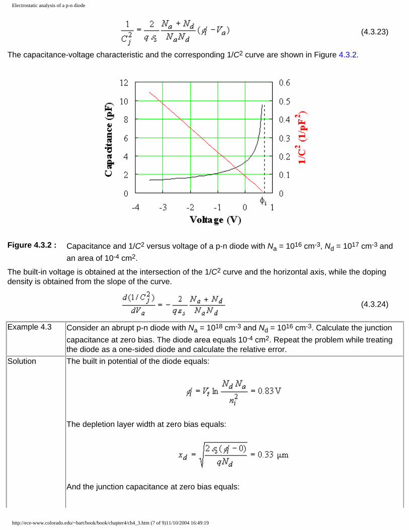
Electrostatic analysis of a p-n diode
(4.3.23)
The capacitance-voltage characteristic and the corresponding 1/C2 curve are shown in Figure 4.3.2.
Figure 4.3.2 : Capacitance and 1/C2 versus voltage of a p-n diode with Na = 1016 cm-3, Nd = 1017 cm-3 and an area of 10-4 cm2.
The built-in voltage is obtained at the intersection of the 1/C2 curve and the horizontal axis, while the doping density is obtained from the slope of the curve.
(4.3.24)
Example 4.3 Consider an abrupt p-n diode with Na = 1018 cm-3 and Nd = 1016 cm-3. Calculate the junction capacitance at zero bias. The diode area equals 10-4 cm2. Repeat the problem while treating the diode as a one-sided diode and calculate the relative error.
Solution The built in potential of the diode equals:
The depletion layer width at zero bias equals:
And the junction capacitance at zero bias equals:
http://ece-www.colorado.edu/~bart/book/book/chapter4/ch4_3.htm (7 of 9)11/10/2004 16:49:19

Electrostatic analysis of a p-n diode
Repeating the analysis while treating the diode as a one-sided diode, one only has to consider the region with the lower doping density so that
And the junction capacitance at zero bias equals
The relative error equals 0.5 %, which justifies the use of the one-sided approximation.
A capacitance-voltage measurement also provides the doping density profile of one-sided p-n diodes. For a p+-n diode, one obtains the doping density from:
(4.3.25)
while the depth equals the depletion layer width which is obtained from xd = εsA/Cj. Both the doping density and the corresponding depth can be obtained at each voltage, yielding a doping density profile. Note that the capacitance in equations (4.3.21), (4.3.22), (4.3.23), and (4.3.25) is a capacitance per unit area.
As an example, we consider the measured capacitance-voltage data obtained on a 6H-SiC p-n diode. The diode consists of a highly doped p-type region on a lightly doped n-type region on top of a highly doped n-type substrate. The measured capacitance as well as 1/C2 is plotted as a function of the applied voltage. The dotted line forms a reasonable fit at voltages close to zero from which one can conclude that the doping density is almost constant close to the p-n interface. At large negative voltages the capacitance becomes almost constant which corresponds to a high doping density according to equation (4.3.25).
http://ece-www.colorado.edu/~bart/book/book/chapter4/ch4_3.htm (8 of 9)11/10/2004 16:49:19

Electrostatic analysis of a p-n diode
Figure 4.3.3 : Capacitance and 1/C2 versus voltage of a 6H-SiC p-n diode.The doping profile calculated from the date presented in Figure 4.3.3 is shown in Figure 4.3.4. The figure confirms the presence of the highly doped substrate and yields the thickness of the n-type layer. No information is obtained at the interface (x = 0) as is typical for doping profiles obtained from C-V measurements. This is because the capacitance measurement is limited to small forward bias voltages since the forward bias current and the diffusion capacitance affect the accuracy of the capacitance measurement.
Figure 4.3.4 : Doping profile corresponding to the measured data, shown in Figure 4.3.3.
http://ece-www.colorado.edu/~bart/book/book/chapter4/ch4_3.htm (9 of 9)11/10/2004 16:49:19

4.3.6. The abrupt p-i-n junction
For a p-i-n junction the above expressions take the following modified form:
aiupn V−=++ φφφφ (4.3.36)
s
pau
s
pap
s
ndn
dxqNxqNxqNε
φε
φε
φ === and 2
, 2
22
(4.3.37)
ndpa xqNxqN = (4.3.38)
Where φu is the potential across the middle undoped region of the diode, which has a thickness d. Equations (4.3.36) through (4.3.38) can be solved for xn yielding:
a
d
aida
das
n
NN
dVNNNN
qd
x+
−−+
+
=1
)()(22 φ
ε
(4.3.39)
From xn and xp, all other parameters of the p-i-n junction can be obtained. The total depletion layer width, xd, is obtained from:
dV
NNNN
qdx ai
da
dasn −−
++= )(
)(22 φε
(4.3.40)
The potential throughout the structure is given by:
2)(2
)( ns
d xxqN
x +−=ε
φ 0<<− xxn (4.3.41)
x
xqNx
s
ndn ε
φφ −−=)( dx <<0 (4.3.42)
2)(2
)()( ps
aai xdx
qNVx −−+−−=
εφφ pxdxd +<<
(4.3.43)
where the potential at x = -xn was assumed to be zero.

4.3.6.1. Capacitance of the p-i-n junction
The capacitance of a p-i-n diode can be obtained from the series connection of the capacitances of each region, simply by adding both depletion layer widths and the width of the undoped region:
d
s
pn
sj xdxx
Cεε
=++
= (4.3.44)

4.3.7. Solution to Poisson’s Equation for an Abrupt p-n Junction
Applying Gauss's law one finds that the total charge in the n-type depletion region equals minus the charge in the p-type depletion region:
psn QxQ −=== )0(Eε (4.3.45)
Poisson's equation can be solved separately in the n and p-type region as was done in section 3.1.1 yielding an expression for E(x = 0) which is almost identical to equation [3.1.4]:
)1(exp2)1(exp2)0(
,,−−=−−==
t
p
t
p
nD
t
t
n
t
n
nD
tVVL
VVVL
Vx
φφφφE (4.3.46)
where φn and φp are assumed negative if the semiconductor is depleted. Their relation to the applied voltage is given by:
iapn V φφφ −=+ (4.3.47)
Solving the transcendental equations one finds φn and φp as a function of the applied voltage. In the special case of a symmetric doping profile, or Nd = Na these equations can easily be solved yielding:
2
iapn
V φφφ
−==
(4.3.48)
The depletion layer widths also equal each other and are given by:
d
s
a
p
d
npn qN
xqN
Q
qNQ
xx)0( =
====Eε
(4.3.49)
Using the above expression for the electric field at the origin we find:
t
tai
t
iaDpn V
VVV
VLxx
−−+
−==
φφ2
exp2 (4.3.50)
where LD is the extrinsic Debye length. The relative error of the depletion layer width as obtained using the full depletion approximation equals:

)2
exp()(2
1
)2
exp()(2
11
t
ia
ai
t
ai
t
t
ia
ai
t
ai
t
p
p
n
n
VV
VV
VV
VV
VV
VV
x
x
xx
φφφ
φφφ
−−
+−
−
−−
+−
−−
=∆
=∆
(4.3.51)
for t
aiV
V−φ = 1, 2, 5, 10, 20 and 40 one finds the relative error to be 45, 23, 10, 5.1, 2.5 and 1.26
%.

4.3.8. The hetero p-n junction
The heterojunction p-n diode is in principle very similar to a homojunction. The main problem that needs to be tackled is the effect of the bandgap discontinuities and the different material parameters, which make the actual calculations more complex even though the p-n diode concepts need almost no changing. An excellent detailed treatment can be found in Wolfe et al.1.
4.3.8.1.Band diagram of a heterojunction p-n diode under Flatband conditions
The flatband energy band diagram of a heterojunction p-n diode is shown in the figure below. As a convention we will assume ∆Ec to be positive if Ec,n > Ec,p and ∆Ev to be positive if Ev,n < Ev,p.
cn
vn
vpFp
cpqφ
∆E
∆E
0
Fn
p
qχ
i
qχn
EE
E
E
EE
E
c
v
Figure 4.3.5 Flat-band energy band diagram of a p-n heterojunction
4.3.8.2.Calculation of the contact potential (built-in voltage)
The built-in potential is defined as the difference between the Fermi levels in both the n-type and the p-type semiconductor. From the energy diagram we find:
pFpcncncnFpFnFi EEEEEEEq ,,,,,,, −++−=−=φ (4.3.52)
which can be expressed as a function of the electron concentrations and the effective densities of states in the conduction band:
1Wolfe, C. Holonyak, N. Stillman, G. Physical properties of semiconductors, Prentice Hall, Chapter 9.

ncp
pcnci Nn
NnkTEq
,0
,0ln+∆=φ (4.3.53)
The built-in voltage can also be related to the hole concentrations and the effective density of states of the valence band:
pvn
nvpvi Np
NpkTEq
,0
,0ln+∆−=φ (4.3.54)
Combining both expressions yields the built-in voltage independent of the free carrier concentrations:
pvnc
pcnv
pini
advci NN
NNkTnnNN
kTEE
q,,
,,
,,ln
2ln
2++
∆−∆=φ
(4.3.55)
where nin and nip are the intrinsic carrier concentrations of the n and p-type region, respectively. ∆Ec and ∆Ev are positive quantities if the bandgap of the n-type region is smaller than that of the p-type region and the sum of both equals the bandgap difference. The above expression reduces to that of the built-in junction of a homojunction if the material parameters in the n-type region equal those in the p-type region. If the effective densities of states are the same the expression reduces to:
pini
advci nn
NNkT
EEq
,,ln
2+
∆−∆=φ
(4.3.56)
4.3.8.3.Abrupt p-n junction
For the calculation of the charge, field and potential distribution in an abrupt p-n junction we follow the same approach as for the homojunction. First of all we use the full depletion approximation and solve Poisson's equation. The expressions derived in section 4.1.1 then still apply.
aipn V−=+ φφφ (4.3.57)
ns
ndn
xqN
,
2
2εφ = and
ps
nap
xqN
,
2
2εφ =
(4.3.58)
ndpa xqNxqN = (4.3.59)
The main differences are the different expression for the built-in voltage and the discontinuities in the field distribution (because of the different dielectric constants of the two regions) and in the energy band diagram. However the expressions for xn and xp for a homojunction can still be
used if one replaces Na by Nas
ps
ε
ε , , Nd by Nds
ns
ε
ε , , xp by xpps
s
,εε
, and xn by xnns
s
,εε
. Adding xn
and xp yields the total depletion layer width xd:

)()()(2
,,
2,,
nsdpsada
aidapsnspnd NNNN
VNNq
xxxεε
φεε
+−+
=+= (4.3.60)
The capacitance per unit area can be obtained from the series connection of the capacitance of each layer:
))((21
,,
,,
,,
ainsdpsa
dapsns
ps
p
ns
nj VNN
NNqxx
C−+
=+
=φεε
εε
εε
(4.3.61)
4.3.8.4.Abrupt P-i-N junction
For a P-i-N junction the above expressions take the following modified form:
aiupn V−=++ φφφφ (4.3.62)
ns
ndn
xqN
,
2
2εφ = ,
ps
pap
xqN
,
2
2εφ = and
us
pau
dxqN
,2εφ =
(4.3.63)
ndpa xqNxqN = (4.3.64)
Where φu is the potential across the middle undoped region of the diode, having a thickness d. The depletion layer width and the capacitance are given by:
xd = xn + xp + d (4.3.65)
sps
p
ns
nj dxx
C
εεε++
=
,,
1
(4.3.66)
Equations [4.2.11] through [4.2.13] can be solved for xn yielding:
)1(
)1()(2
)(,
,,2
,
,
a
d
us
ns
a
d
d
ains
us
ns
n
NN
d
NN
qN
Vd
x+
−+−
+
=ε
εφε
ε
ε
(4.3.67)
A solution for xp can be obtained from [4.2.16] by replacing Nd by Na, Na by Nd, εs,n by εs,p, and εs,p by εs,n. Once xn and xp are determined all other parameters of the P-i-N junction can be

obtained. The potential throughout the structure is given by:
2
,)(
2)( n
ns
d xxqN
x +−=ε
φ for -xn <x < 0 (4.3.68)
x
xqNx
ns
ndn
,2)(
εφφ −−= for 0 <x < d
(4.3.69)
2
,)(
2)()( p
ps
aai xdx
qNVx −−+−−=
εφφ for d < x < d + xp
(4.3.70)
where the potential at x = -xn was assumed to be zero.
x [nm]
Cha
rge
Den
sity
[C/c
m3]
-0.02
-0.015
-0.01
-0.005
0
0.005
0.01
0.015
0.02
-200 -150 -100 -50 0 50 100 150 200
x [nm]
Ele
ctri
c F
ield
[V/c
m]
0
20000
40000
60000
80000
100000
120000
140000
-200 -150 -100 -50 0 50 100 150 200
x [nm]
Pot
enti
al [V
]
0
0.2
0.4
0.6
0.8
1
1.2
-200 -150 -100 -50 0 50 100 150 200
x [nm]
Ele
ctro
n E
nerg
y [E
v]
-2
-1.5
-1
-0.5
0
0.5
1
-200 -150 -100 -50 0 50 100 150 200
Ev
Ei
Ec
Fn
Fp
Figure 4.3.6 Charge distribution, electric field, potential and energy band diagram of an
AlGaAs/GaAs p-n heterojunction with Va = 0.5 V, x = 0.4 on the left and x = 0 on the right. Nd = Na = 1017cm-3
The above derivation ignores the fact that, because of the energy band discontinuities, the carrier densities in the intrinsic region could be substantially larger than in the depletion regions in the n-type and p-type semiconductor. Large amounts of free carriers imply that the full depletion approximation is not valid and that the derivation has to be repeated while including a possible charge in the intrinsic region.
4.3.8.5.A P-M-N junction with interface charges
Real P-i-N junctions often differ from their ideal model, which was described in section b). The

intrinsic region could be lightly doped, while a fixed interface charge could be present between the individual layers. Assume the middle layer to have a doping concentration Nm = Ndm - Nam and a dielectric constant εs,m. A charge Q1 is assumed between the N and M layer, and a charge Q2 between the M and P layer. Equations [4.2.11] through [4.2.13] then take the following form:
aimpn V−=++ φφφφ (4.3.71)
ns
ndn
xqN
,
2
2εφ = ,
ps
pap
xqN
,
2
2εφ = and
ms
m
mspam
dqNdQxqN
,
2
,1 2)(
εεφ ++=
(4.3.72)
pamnd xqNdqNQQxqN =+++ 21 (4.3.73)
These equations can be solved for xn and xp yielding a general solution for this structure. Again it should be noted that this solution is only valid if the middle region is indeed fully depleted.
Solving the above equation allows to draw the charge density, the electric field distribution, the potential and the energy band diagram.
x [nm]
Cha
rge
Den
sity
[C/c
m3]
-0.02
-0.015
-0.01
-0.005
0
0.005
0.01
0.015
0.02
-80 -60 -40 -20 0 20 40 60 80
x [nm]
Ele
ctri
c F
ield
[V/c
m]
0
10000
20000
30000
40000
50000
60000
-80 -60 -40 -20 0 20 40 60 80
x [nm]
Pot
enti
al [V
]
0
0.05
0.1
0.15
0.2
0.25
-80 -60 -40 -20 0 20 40 60 80
x [nm]
Ele
ctro
n E
nerg
y [E
v]
-2
-1.5
-1
-0.5
0
0.5
-80 -60 -40 -20 0 20 40 60 80
Ev
Ei
EcFn
Fp
Figure 4.3.7 Charge distribution, electric field, potential and energy band diagram of an
AlGaAs/GaAs p-i-n heterojunction with Va = 1.4 V, x = 0.4 on the left, x = 0 in the middle and x = 0.2 on the right. d = 10 nm and Nd = Na = 1017cm-3

4.3.8.6.Quantum well in a p-n junction
Consider a p-n junction with a quantum well located between the n and p region as shown in the figure below.
cn
vnvp
fp
cp∆E
∆E
fn
EE
E
E
E
E
c
v
-L 0
x
quantumwell
n -layer p-layer
qφ i
x
Figure 4.3.8 Flat-band energy band diagram of a p-n heterojunction with a quantum well at the interface.
Under forward bias charge could accumulate within the quantum well. In this section we will outline the procedure to solve this structure. The actual solution can only be obtained by solving a transcendental equation. Approximations will be made to obtain useful analytic expressions.
The potentials within the structure can be related to the applied voltage by:
aipqwn V−=++ φφφφ (4.3.74)
where the potentials across the p and n regions are obtained using the full depletion approximation:
ns
ndn
xqN
,
2
2εφ = , and
ps
pap
xqN
,
2
2εφ =
(4.3.75)
The potential across the quantum well is to first order given by:
ps
x
ns
xndqw
LNPqLxqN
,, 2)(
2 εεφ
−+=
(4.3.76)
where P and N are the hole respectively electron densities per unit area in the quantum well. This equation assumes that the charge in the quantum well Q = q (P - N) is located in the middle of the well. Applying Gauss's law to the diode yields the following balance between the charges:

pand xqNqPqNxqN +−=− (4.3.77)
where the electron and hole densities can be expressed as a function of the effective densities of states in the quantum well:
∑∞
=
∆+=
1
,, ]exp1ln[
n
enqwc kT
ENN
(4.3.78)
∑∞
=
∆+=
1
,, ]exp1ln[
n
hnqwv kT
EPP
(4.3.79)
with ∆En,e and ∆En,h given by:
en
d
ncncen E
N
NkTqEE ,
,, ln −−−∆=∆ φ
(4.3.80)
hn
a
pvpvhn E
N
NkTqEE ,
,, ln −−−∆=∆ φ
(4.3.81)
where En,e and En,h are the nth energies of the electrons respectively holes relative to the conduction respectively valence band edge. These nine equations can be used to solve for the nine unknowns by applying numerical methods. A quick solution can be obtained for a symmetric diode, for which all the parameters (including material parameters) of the n and p region are the same. For this diode N equals P because of the symmetry. Also xn equals xp and φn equals φp. Assuming that only one energy level namely the n = 1 level is populated in the quantum well one finds:
]
2
2exp1ln[ ,1
, kT
EEqVNPN gea
qwc−−
+== (4.3.82)
where Eg is the bandgap of the quantum well material.
Numeric simulation for the general case reveal that, especially under large forward bias conditions, the electron and hole density in the quantum well are the same to within a few percent. An energy band diagram calculated using the above equations is shown in the figure below:

x [nm]
Cha
rge
Den
sity
[C/c
m3]
-0.08
-0.06
-0.04
-0.02
0
0.02
0.04
0.06
0.08
-30 -20 -10 0 10 20 30
x [nm]
Ele
ctri
c F
ield
[V/c
m]
0
10000
20000
30000
40000
50000
60000
-30 -20 -10 0 10 20 30
x [nm]
Pot
enti
al [V
]
0
0.01
0.02
0.03
0.04
0.05
0.06
0.07
0.08
0.09
0.1
-30 -20 -10 0 10 20 30
x [nm]
Ele
ctro
n E
nerg
y [E
v]
-1.8
-1.6
-1.4
-1.2
-1
-0.8
-0.6
-0.4
-0.2
0
0.2
-30 -20 -10 0 10 20 30
Ev
Ei
EcFn
Fp
x [nm]
Ele
ctro
n E
nerg
y [E
v]
-0.15
-0.1
-0.05
0
0.05
0.1
0.15
-30 -20 -10 0 10 20 30
Ec
Fn
E1p
E2n
x [nm]
Ele
ctro
n E
nerg
y [E
v]
-1.7
-1.65
-1.6
-1.55
-1.5
-1.45
-1.4
-30 -20 -10 0 10 20 30
Ev
Fp
E1p E2p
E3p
E4p
Figure 4.3.9 Energy band diagram of a GaAs/AlGaAs p-n junction with a quantum well in
between. The aluminum concentration is 40 % for both the p and n region, and zero in the well. The doping concentrations Na and Nd are 4 x 1017 cm-3 and Va = 1.4 V.
From the numeric simulation of a GaAs n-qw-p structure we find that typically only one electron level is filled with electrons, while several hole levels are filled with holes or
...3211 +++=≅= PPPPNN (4.3.83)
If all the quantized hole levels are more than 3kT below the hole quasi-Fermi level one can rewrite the hole density as:
∑
−=
n
hnh
kT
EEPP ,,11 exp
(4.3.84)
and the applied voltage is given by:
)1)(1ln(
*//1, −−+= vc NNNNt
qwga eeV
q
EV
(4.3.85)
with
∑
−=
n
hnhvv kT
EENN ,,1* exp
(4.3.86)
...)
15exp
8exp
3exp1( ,1,1,1* +
−+
−+
−+=
kT
E
kT
E
kT
ENN hhh
vv (4.3.87)

The p-n diode current
Title Page Table of Contents Help Copyright B. Van Zeghbroeck, 2004
Chapter 4: p-n Junctions
4.4. The p-n diode current4.4.1. General discussion4.4.2. The ideal diode current4.4.3. Recombination-Generation current4.4.4. I-V characteristics of real p-n diodes4.4.5. The diffusion capacitance
4.4.1. General discussion
The current in a p-n diode is due to carrier recombination or generation somewhere within the p-n diode structure. Under forward bias, the diode current is due to recombination. This recombination can occur within the quasi-neutral semiconductor, within the depletion region or at the metal-semiconductor Ohmic contacts. Under reverse bias, the current is due to generation. Carrier generation due to light will further increase the current under forward as well as reverse bias. In this section, we first derive the ideal diode current. We will also distinguish between the "long" diode and "short" diode case. The "long" diode expression applies to p-n diodes in which recombination/generation occurs in the quasi-neutral region only. This is the case if the quasi-neutral region is much larger than the carrier diffusion length. The "short" diode expression applies to p-n diodes in which recombination/generation occurs at the contacts only. In a short diode, the quasi-neutral region is much smaller than the diffusion length. In addition to the "long" and "short" diode expressions, we also present the general result, which deals with recombination/generation in a finite quasi-neutral region.Next, we derive expressions for the recombination/generation in the depletion region. Here we have to distinguish between the different recombination mechanisms - band-to-band recombination and Shockley-Hall-Read recombination - as they lead to different current-voltage characteristics.
4.4.2. The ideal diode current
4.4.2.1. General discussion and overview
When calculating the current in a p-n diode one needs to know the carrier density and the electric field throughout the p-n diode which can then be used to obtain the drift and diffusion current. Unfortunately, this requires the knowledge of the quasi-Fermi energies, which is only known if the currents are known. The straightforward approach is to simply solve the drift-diffusion equation listed in section 2.10 simultaneously. This approach however does not yield an analytic solution.
http://ece-www.colorado.edu/~bart/book/book/chapter4/ch4_4.htm (1 of 14)11/10/2004 16:49:55

The p-n diode current
To avoid this problem we will assume that the electron and hole quasi-Fermi energies in the depletion region equal those in the adjacent n-type and p-type quasi-neutral regions. We will derive an expression for "long" and "short" diodes as well as a general expression, which is to be used if the quasi-neutral region is comparable in size to the diffusion length.
4.4.2.2. Assumptions and boundary conditions
The electric field and potential are obtained by using the full depletion approximation. Assuming that the quasi-Fermi energies are constant throughout the depletion region, one obtains the minority carrier densities at the edges of the depletion region, yielding:
(4.4.1)
and
(4.4.2)
These equations can be verified to yield the thermal-equilibrium carrier density for zero applied voltage. In addition, an increase of the applied voltage will increase the separation between the two quasi-Fermi energies by the applied voltage multiplied with the electronic charge and the carrier density depends exponentially on this quantity.The carrier density at the metal contacts is assumed to equal the thermal-equilibrium carrier density. This assumption implies that excess carriers immediately recombine when reaching either of the two metal-semiconductor contacts. As recombination is typically higher at a semiconductor surface and is further enhanced by the presence of the metal, this is found to be a reasonable assumption. This results in the following set of boundary conditions:
(4.4.3)
and
(4.4.4)
4.4.2.3. General current expression
The general expression for the ideal diode current is obtained by applying the boundary conditions to the general solution of the diffusion equation for each of the quasi-neutral regions, as described by equation (2.9.13) and (2.9.14):
(2.9.13)
(2.9.14)
The boundary conditions at the edge of the depletion regions are described by (4.4.1), (4.4.2), (4.4.3) and (4.4.4).
Before applying the boundary conditions, it is convenient to rewrite the general solution in terms of hyperbolic functions:
(4.4.5)
http://ece-www.colorado.edu/~bart/book/book/chapter4/ch4_4.htm (2 of 14)11/10/2004 16:49:55
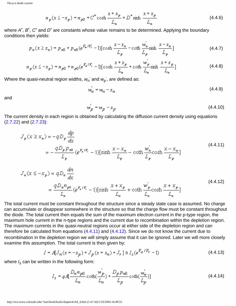
The p-n diode current
(4.4.6)
where A*, B*, C* and D* are constants whose value remains to be determined. Applying the boundary conditions then yields:
(4.4.7)
(4.4.8)
Where the quasi-neutral region widths, wn' and wp', are defined as:
(4.4.9)
and
(4.4.10)
The current density in each region is obtained by calculating the diffusion current density using equations (2.7.22) and (2.7.23):
(4.4.11)
(4.4.12)
The total current must be constant throughout the structure since a steady state case is assumed. No charge can accumulate or disappear somewhere in the structure so that the charge flow must be constant throughout the diode. The total current then equals the sum of the maximum electron current in the p-type region, the maximum hole current in the n-type regions and the current due to recombination within the depletion region. The maximum currents in the quasi-neutral regions occur at either side of the depletion region and can therefore be calculated from equations (4.4.11) and (4.4.12). Since we do not know the current due to recombination in the depletion region we will simply assume that it can be ignored. Later we will more closely examine this assumption. The total current is then given by:
(4.4.13)
where Is can be written in the following form:
(4.4.14)
http://ece-www.colorado.edu/~bart/book/book/chapter4/ch4_4.htm (3 of 14)11/10/2004 16:49:55

The p-n diode current
4.4.2.4. The p-n diode with a "long" quasi-neutral region
A diode with a "long" quasi-neutral region has a quasi-neutral region which is much larger than the minority-carrier diffusion length in that region, or wn' > Lp and wp' > Ln. The general solution can be simplified under those conditions using:
(4.4.15)
Yielding the following carrier densities, current densities and saturation currents:
(4.4.16)
(4.4.17)
(4.4.18)
(4.4.19)
(4.4.20)
We now come back to our assumption that the current due to recombination in the depletion region can be simply ignored. Given that there is recombination in the quasi-neutral region, it would be unreasonable to suggest that the recombination rate would simply drop to zero in the depletion region. Instead, we assume that the recombination rate is constant in the depletion region. To further simplify the analysis we will consider a p+-n junction so that we only need to consider the recombination in the n-type region. The current due to recombination in the depletion region is then given by:
(4.4.21)
so that Ir can be ignored if:
(4.4.22)
A necessary, but not sufficient requirement is therefore that the depletion region width is much smaller than the diffusion length for the ideal diode assumption to be valid. Silicon and germanium p-n diodes usually satisfy this requirement, while gallium arsenide p-n diodes rarely do because of the short carrier lifetime and diffusion length.
As an example we now consider a silicon p-n diode with Na = 1.5 x 1014 cm-3 and Nd = 1014 cm-3. The minority carrier lifetime was chosen to be very short, namely 400 ps, so that most features of interest can be easily observed. We start by examining the electron and hole density throughout the p-n diode, shown in Figure 4.4.1:
http://ece-www.colorado.edu/~bart/book/book/chapter4/ch4_4.htm (4 of 14)11/10/2004 16:49:55

The p-n diode current
Figure 4.4.1 : Electron and hole density throughout a forward biased p-n diode.
The majority carrier densities in the quasi-neutral region simply equal the doping density. The minority carrier densities in the quasi-neutral regions are obtained from the equations (4.4.16) and (4.4.17). The electron and hole densities in the depletion region are calculating using the assumption that the electron/hole quasi-Fermi energy in the depletion region equals the electron/hole quasi-Fermi energy in the quasi-neutral n-type/p-type region. The corresponding band diagram is shown in Figure 4.4.2:
Figure 4.4.2 : Energy band diagram of a p-n diode. Shown are the conduction band edge, Ec, and the valence band edge, Ev, the intrinsic energy, EI, the electron quasi-Fermi energy, Fn, and the hole quasi-Fermi energy, Fp.
The quasi-Fermi energies were obtained by combining (4.4.16) and (4.4.17) with (2.6.37) and (2.6.38). Note that the quasi-Fermi energies vary linearly within the quasi-neutral regions.
http://ece-www.colorado.edu/~bart/book/book/chapter4/ch4_4.htm (5 of 14)11/10/2004 16:49:55

The p-n diode current
Next, we discuss the current density. Shown in Figure 4.4.3 is the electron and hole current density as calculated using (4.4.18) and (4.4.19). The current due to recombination in the depletion region was assumed to be constant.
Figure 4.4.3 : Electron and hole current density versus position. The vertical lines indicate the edges of the depletion region.
4.4.2.5. The p-n diode with a "short" quasi-neutral region
A "short" diode is a diode with quasi-neutral regions, which are much shorter than the minority-carrier diffusion lengths. As the quasi-neutral region is much smaller than the diffusion length one finds that recombination in the quasi-neutral region is negligible so that the diffusion equations are reduced to:
(4.4.23)
The resulting carrier density varies linearly throughout the quasi-neutral region and in general is given by:
(4.4.24)
where A, B, C and D are constants obtained by satisfying the boundary conditions. Applying the same boundary conditions at the edge of the depletion region as above (equations (4.4.3) and (4.4.4)) and requiring thermal equilibrium at the contacts yields:
(4.4.25)
(4.4.26)
for the hole and electron density in the n-type quasi-neutral region.
http://ece-www.colorado.edu/~bart/book/book/chapter4/ch4_4.htm (6 of 14)11/10/2004 16:49:55

The p-n diode current
The current in a "short" diode is again obtained by adding the maximum diffusion currents in each of the quasi-neutral regions and ignoring the current due to recombination in the depletion region, yielding:
(4.4.27)
where the saturation current, Is is given by:
(4.4.28)
A comparison of the "short" diode expression with the "long" diode expression reveals that they are the same except for the use of either the diffusion length or the quasi-neutral region width in the denominator, whichever is smaller. Given that we now have two approximate expressions, it is of interest to know when to use one or the other. To this end, we now consider a one-sided n+-p diode. The p-type semiconductor has a width wp and we normalize the excess electron density relative to its value at x = 0. The Ohmic contact to the p-type region is ideal so that the excess density is zero at x = wp'. The normalized excess carrier density is shown in Figure 4.4.4 for different values of the diffusion length.
Figure 4.4.4 : Excess electron density versus position as obtained by solving the diffusion equation with δn(x = 0) = 1 and δn(x/wp' = 1) = 0 . The ratio of the diffusion length to the width of the quasi-neutral region is varied from 0.1 (Bottom curve), 0.3, 0.5, 1 and 10 (top curve)
The figure illustrates how the excess electron density changes as the diffusion length is varied relative to the width of the quasi-neutral region. For the case where the diffusion length is much smaller than the width (Ln << wp'), the electron density decays exponentially and the "long" diode expression can be used. If the diffusion length is much longer than the width (Ln >> wp'), the electron density reduces linearly with position and the "short" diode expression can be used. If the diffusion length is comparable to the width of the quasi-neutral region width one must use the general expression. A numeric analysis reveals that the error is less than 10 % when using the short diode expression with Ln > wp'/2 and when using the long diode expression with Ln > 2 wp'.
http://ece-www.colorado.edu/~bart/book/book/chapter4/ch4_4.htm (7 of 14)11/10/2004 16:49:55
The p-n diode current
Example 4.4 An abrupt silicon p-n junction (Na = 1016 cm-3 and Nd = 4 x 1016 cm-3) is biased with Va = 0.6 V. Calculate the ideal diode current assuming that the n-type region is much smaller than the diffusion length with wn' = 1 µm and assuming a "long" p-type region. Use µn = 1000 cm2/V-s and µp = 300 cm2/V-s. The minority carrier lifetime is 10 µs and the diode area is 100 µm by 100 µm.
Solution The current is calculated from:
with
Dn = µn Vt = 1000 x 0.0258 = 25.8 cm2/V-s
Dp = µp Vt = 300 x 0.0258 = 7.75 cm2/V-s
np0 = ni2/Na = 1020/1016 = 104 cm-3
pn0 = ni2/Nd = 1020/4 x 1016 = 2.5 x 103 cm-3
yielding I = 40.7 mA
Note that the hole diffusion current occurs in the "short" n-type region and therefore depends on the quasi-neutral width in that region. The electron diffusion current occurs in the "long" p-type region and therefore depends on the electron diffusion length in that region.
4.4.3. Recombination-Generation current
4.4.3.1. Band-to-band Recombination-Generation current
The recombination/generation current due to band-to-band recombination/generation is obtained by integrating the net recombination rate, Ub-b, over the depletion region:
(4.4.29)
where the net recombination rate is given by:
(4.4.30)
http://ece-www.colorado.edu/~bart/book/book/chapter4/ch4_4.htm (8 of 14)11/10/2004 16:49:55

The p-n diode current
The carrier densities can be related to the constant quasi-Fermi energies and the product is independent of position:
(4.4.31)
This allows the integral to be solved analytically yielding:
(4.4.32)
The current due to band-to-band recombination has therefore the same voltage dependence as the ideal diode current and simply adds an additional term to the expression for the saturation current.
4.4.3.2. Shockley-Hall-Read Recombination-Generation current
The current due to trap-assisted recombination in the depletion region is also obtained by integrating the trap-assisted recombination rate over the depletion region width:
(4.4.33)
Substituting the expression for the recombination rate yields:
(4.4.34)
where the product of the electron and hole densities was obtained by assuming that the quasi-Fermi energies are constant throughout the depletion region, which leads to:
(4.4.35)
The maximum recombination rate is obtained when the electron and hole densities are equal and therefore equals the square root of the product yielding:
(4.4.36)
From which an effective width can be defined which, when multiplied with the maximum recombination rate, equals the integral of the recombination rate over the depletion region. This effective width, x', is then defined by:
(4.4.37)
and the associated current due to trap-assisted recombination in the depletion region is given by:
(4.4.38)
http://ece-www.colorado.edu/~bart/book/book/chapter4/ch4_4.htm (9 of 14)11/10/2004 16:49:55

The p-n diode current
This does not provide an actual solution since the effective width, x', still must be determined by performing a numeric integration. Nevertheless, the above expression provides a way to obtain an upper estimate by substituting the depletion layer width, xd, as it is always larger than the effective width.
4.4.4. I-V characteristics of real p-n diodes
The forward biased I-V characteristics of real p-n diodes are further affected by high injection and the series resistance of the diode. To illustrate these effects while summarizing the current mechanisms discussed previously we consider the I-V characteristics of a silicon p+-n diode with Nd = 4 x 1014 cm-3, τp = 10 ms, and µp = 450 cm2/V-s. The I-V characteristics are plotted on a semi-logarithmic scale and four different regions can be distinguished as indicated on Figure 4.4.5. First, there is the ideal diode region where the current increases by one order of magnitude as the voltage is increased by 60 mV. This region is referred to as having an ideality factor, n, of one. This ideality factor is obtained by fitting a section of the curve to the following expression for the current:
(4.4.39)
The ideality factor can also be obtained from the slope of the curve on a semi-logarithmic scale using:
(4.4.40)
where the slope is in units of V/decade. To the left of the ideal diode region there is the region where the current is dominated by the trap-assisted recombination in the depletion region described in section 4.4.3.2. This part of the curve has an ideality factor of two. To the right of the ideal diode region, the current becomes limited by high injection effects and by the series resistance.High injection occurs in a forward biased p-n diode when the injected minority carrier density exceeds the doping density. High injection will therefore occur first in the lowest doped region of the diode since that region has the highest minority carrier density.
Using equations (4.4.1) and (4.4.2), one finds that high injection occurs in a p+-n diode for the following applied voltage:
(4.4.41)
or at Va = 0.55 V for the diode of Figure 4.4.5 as can be verified on the figure as the voltage where the ideality factor changes from one to two. For higher forward bias voltages, the current does no longer increase exponentially with voltage. Instead, it increases linearly due to the series resistance of the diode. This series resistance can be due to the contact resistance between the metal and the semiconductor, due to the resistivity of the semiconductor or due to the series resistance of the connecting wires. This series resistance increases the external voltage, Va*, relative to the internal voltage, Va, considered so far.
(4.4.42)
Where I is the diode current and Rs is the value of the series resistance.
These four regions can be observed in most p-n diodes although the high-injection region rarely occurs, as the series resistance tends to limit the current first.
http://ece-www.colorado.edu/~bart/book/book/chapter4/ch4_4.htm (10 of 14)11/10/2004 16:49:55

The p-n diode current
Figure 4.4.5: Current-Voltage characteristics of a silicon diode under forward bias.
4.4.5. The diffusion capacitance
As a p-n diode is forward biased, the minority carrier distribution in the quasi-neutral region increases dramatically. In addition, to preserve quasi-neutrality, the majority carrier density increases by the same amount. This effect leads to an additional capacitance called the diffusion capacitance. The diffusion capacitance is calculated from the change in charge with voltage:
(4.4.43)
Where the charge, ∆Q, is due to the excess carriers. Unlike a parallel plate capacitor, the positive and negative charge is no longer separated in space. Instead, the electrons and holes are separated by the energy bandgap. Nevertheless, these voltage dependent charges yield a capacitance just as the one associated with a parallel plate capacitor. The excess minority-carrier charge is obtained by integrating the charge density over the quasi-neutral region:
(4.4.44)
We now distinguish between the two limiting cases as discussed when calculating the ideal diode current, namely the "long" diode and a "short" diode. The carrier distribution, pn(x), in a "long" diode is illustrated by Figure 4.4.6 (a).
http://ece-www.colorado.edu/~bart/book/book/chapter4/ch4_4.htm (11 of 14)11/10/2004 16:49:55
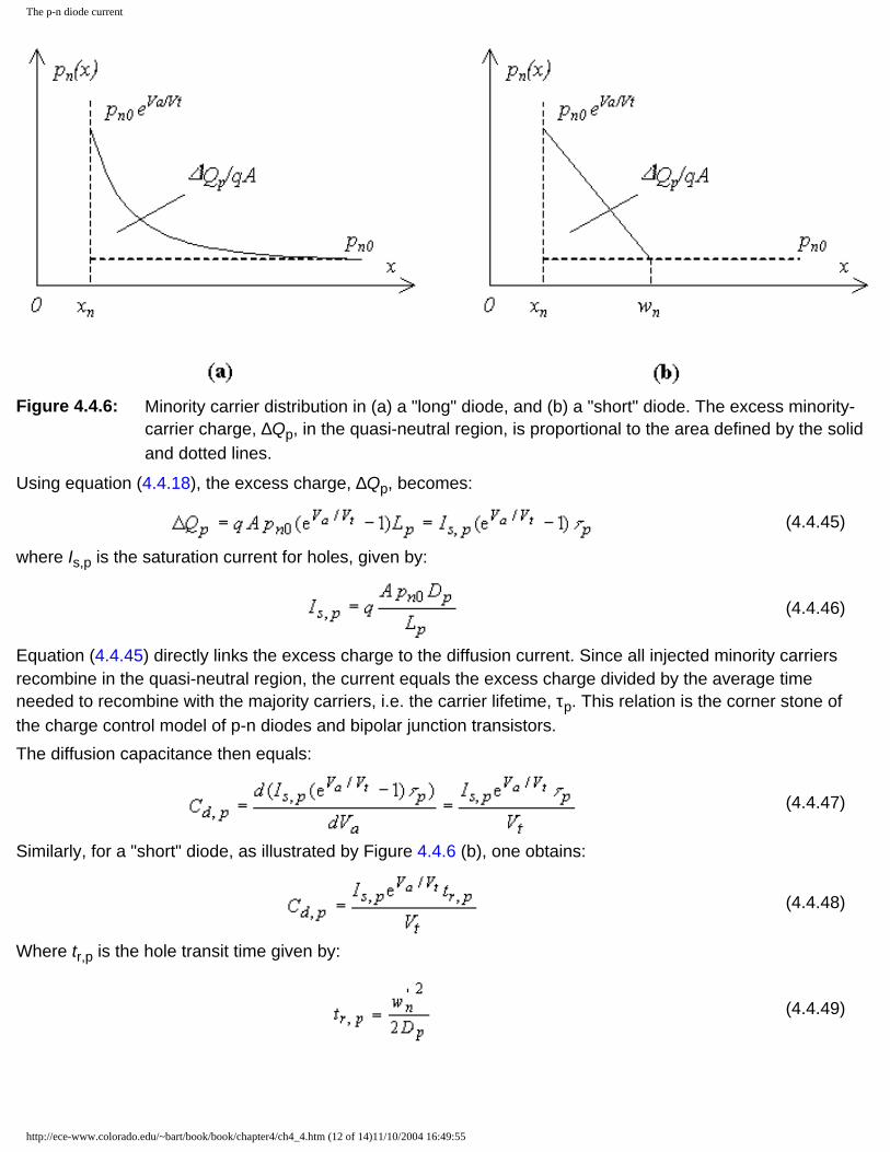
The p-n diode current
Figure 4.4.6: Minority carrier distribution in (a) a "long" diode, and (b) a "short" diode. The excess minority-carrier charge, ∆Qp, in the quasi-neutral region, is proportional to the area defined by the solid and dotted lines.
Using equation (4.4.18), the excess charge, ∆Qp, becomes:
(4.4.45)
where Is,p is the saturation current for holes, given by:
(4.4.46)
Equation (4.4.45) directly links the excess charge to the diffusion current. Since all injected minority carriers recombine in the quasi-neutral region, the current equals the excess charge divided by the average time needed to recombine with the majority carriers, i.e. the carrier lifetime, τp. This relation is the corner stone of the charge control model of p-n diodes and bipolar junction transistors. The diffusion capacitance then equals:
(4.4.47)
Similarly, for a "short" diode, as illustrated by Figure 4.4.6 (b), one obtains:
(4.4.48)
Where tr,p is the hole transit time given by:
(4.4.49)
http://ece-www.colorado.edu/~bart/book/book/chapter4/ch4_4.htm (12 of 14)11/10/2004 16:49:55

The p-n diode current
Again, the excess charge can be related to the current. However, in the case of a "short" diode all minority carriers flow through the quasi-neutral region and do not recombine with the majority carriers. The current therefore equals the excess charge divided by the average time needed to traverse the quasi-neutral region, i.e. the transit time, tr,p.
The total diffusion capacitance is obtained by adding the diffusion capacitance of the n-type quasi-neutral region to that of the p-type quasi-neutral region.The total capacitance of the junction equals the sum of the junction capacitance, discussed in section 4.3.4, and the diffusion capacitance. For reverse biased voltages and small forward bias voltages, one finds that the junction capacitance is dominant. As the forward bias voltage is further increased the diffusion capacitance increases exponentially and eventually becomes larger than the junction capacitance.Example 4.5 a. Calculate the diffusion capacitance of the diode described in Example 4.4 at zero bias.
Use µn= 1000 cm2/V-s, µp = 300 cm2/V-s, wp' = 1 µm and wn' = 1 mm. The minority carrier lifetime equals 0.1 ms.
b. For the same diode, find the voltage for which the junction capacitance equals the diffusion capacitance.
Solution a. The diffusion capacitance at zero volts equals
using
and
where the "short" diode expression was used for the capacitance associated with the excess charge due to electrons in the p-type region. The "long" diode expression was used for the capacitance associated with the excess charge due to holes in the n-type region.The diffusion constants and diffusion lengths equal
Dn = µn x Vt = 25.8 cm2/s
Dp = µp x Vt = 7.75 cm2/s
http://ece-www.colorado.edu/~bart/book/book/chapter4/ch4_4.htm (13 of 14)11/10/2004 16:49:55

The p-n diode current
And the electron transit time in the p-type region equals
b. The voltage at which the junction capacitance equals the diffusion capacitance is obtained by solving
yielding Va = 0.442 V
http://ece-www.colorado.edu/~bart/book/book/chapter4/ch4_4.htm (14 of 14)11/10/2004 16:49:55

4.4.6. High Injection Effects
High injection of carriers1 causes to violate one of the approximations made in the derivation of the ideal diode characteristics, namely that the majority carrier density equals the thermal equilibrium value. Excess carriers will dominate the electron and hole concentration and can be expressed in the following way:
)()exp( 0
2ppp
t
aipp npn
VV
npn +== (4.4.50)
)()exp( 0
2nnn
t
ainn pnp
VV
npn +== (4.4.51)
where all carrier densities with subscript n are taken at x = xn and those with subscript p at x = -xp. Solving the resulting quadratic equation yields:
)2
exp()1)exp(4
1(2
22
2
t
ai
a
t
ai
ap V
Vn
NVV
nN
n ≅−+=
(4.4.52)
)2
exp()1)exp(4
1(2
22
2
t
ai
d
t
ai
dn V
Vn
NVV
nN
p ≅−+=
(4.4.53)
where the second terms are approximations for large Va. From these expressions one can calculate the minority carrier diffusion current assuming a "long" diode. We also ignore carrier recombination in the depletion region.
)
2exp()(
t
ai
p
p
n
npn V
Vn
L
D
LD
qJJ +=+ (4.4.54)
This means that high injection in a p-n diode will reduce the slope on the current-voltage characteristic on a semi-logarithmic scale to 119mV/decade.
High injection also causes a voltage drop across the quasi-neutral region. This voltage can be calculated from the carrier densities. Let's assume that high injection only occurs in the (lower doped) p-type region. The hole density at the edge of the depletion region (x = xp) equals:
1A more complete derivation can be found in R.S. Muller and T.I. Kamins, "Device Electronics for Integrated Circuits", Wiley and sons, second edition p. 323-324.

)exp()()exp()( 1
01
t
apappa
tapp V
VVnNxxnN
VV
Nxxp−
+==+=== (4.4.55)
where V1 is the voltage drop across the p-type quasi-neutral region. This equation can then be solved for V1 yielding
]2
1)exp(4
1
ln[2
2
1
−+
= a
t
ai
t
NVV
n
VV
(4.4.56)
High injection occurs (by definition) when the excess minority carrier density exceeds the doping density in the material. It is under such conditions that also the majority carrier density increases since, for charge neutrality to exist, the excess electron density has to equal the excess hole density: If there exists a net charge, the resulting electric field causes the carriers to move so that charge neutrality is restored.
Up till now we have assumed that the minority carrier densities in the n-type and p-type region are small compared to the doping density. However as the forward bias voltage is increased the minority carrier density exceeds the doping density.
The analysis starts by assuming a certain excess carrier density so that the total density can be written as the sum of the thermal equilibrium density plus the excess carrier density. For an n-type region this yields the following equations:
nnn nnn δ+= 0 (4.4.57)
npn ppp δ+= 0 (4.4.58)
The product of the carrier densities can be expressed as a function of the intrinsic density in the following way:
))((exp 00
2npnn
t
ainn ppnn
VV
npn δδ ++== (4.4.59)
where it was assumed that the semiconductor is non-degenerate and that the difference between the electron and hole quasi Fermi energies in electron volt equals the applied voltage in volt. Quasi-neutrality implies that the excess densities are the same, which yields a quadratic equation for the minority carrier density pn:
0)1(exp)( 22 =−−+
t
aindn V
VnpNp δδ
(4.4.60)
which yields a value for the minority carrier density at the edge of the depletion region.

)1]1)[exp(4
1(2 2
2
−−
+=d
t
ai
dn N
VV
nN
pδ
(4.4.61)
The associated current is a diffusion current and using a procedure similar to that for calculating the ideal diode current in a "long" diode one obtains the following hole current2.
)1]1)[exp(4
1(2 2
2
−−
+==d
t
ai
p
dp
p
npp N
VV
n
L
NDqA
L
pDqAI
δ
(4.4.62)
The electron current due to diffusion of electrons in the p-type region is given by a similar expression:
)1]1)[exp(4
1(2 2
2
−−
+==a
t
ai
n
an
n
pnn N
VV
n
LND
qAL
nDqAI
δ
(4.4.63)
These expressions can be reduced to the ideal diode expressions provided that the excess minority density is much smaller than one quarter of the doping density, or:
]1)[exp(0 −=
t
a
p
ppp V
VL
nDqAI
, for 4]1)[exp(0
d
t
ap
NVV
n <<− (4.4.64)
while if the excess minority carrier density is much larger than one quarter of the doping density and expression is obtained which is only valid under high injection conditions:
)
2exp(
t
a
p
ipp V
VL
nDqAI =
, for 4]1)[exp(0
d
t
ap
NVV
n >>− (4.4.65)
A closer examination of the problem prompts the question whether the full depletion approximation is still valid since the sign of potential across the semiconductor reverses. However the increase of the majority carrier density beyond the doping density causes a potential variation across the "quasi-neutral" region. This voltage in the n-type region is given by:
2 The reader should note that the potential across the "quasi-neutral" regions goes hand-in-hand with an electric field. The region is therefore not neutral so that the diffusion equation is no longer valid. Instead one has to calculate the current based on the diffusion and drift of the carriers. The equations above were derived using the diffusion equation and should therefore be used with caution.

]2
1)exp(4
1
ln[ln2
2
0
0
−+
=+
== d
t
ai
tn
nntn
NVV
n
Vn
nnVV
δ
(4.4.66)
and similarly for the p-type region:
]2
1)exp(4
1
ln[ln2
2
0
0
−+
=+
== a
t
ai
tp
pptp
NVV
n
Vp
ppVV
δ
(4.4.67)
The potentials across the "quasi-neutral" region causes a larger potential across the depletion layer, since they have opposite sign, so that the depletion layer width as calculated using the modified potential φ = φi – Va + Vn + Vp does not become zero.
As an example we now consider an abrupt one-sided p-n diode. The current is shown as function of the voltage in the figure below. It is calculated for an n-type doping of 1013 cm-3.
Figure 4.4.7 Current-Voltage characteristics of a p+-n diode including the effects of high injection and a linear series resistance.
The dotted line on the figure fits the current at high forward bias. The slope is 1 decade/120 mV which corresponds to an ideality factor of 2.
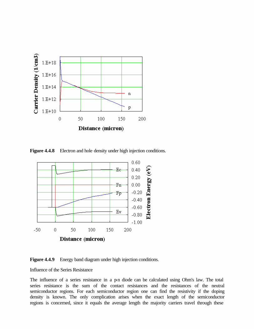
Figure 4.4.8 Electron and hole density under high injection conditions.
Figure 4.4.9 Energy band diagram under high injection conditions.
Influence of the Series Resistance
The influence of a series resistance in a p-n diode can be calculated using Ohm's law. The total series resistance is the sum of the contact resistances and the resistances of the neutral semiconductor regions. For each semiconductor region one can find the resistivity if the doping density is known. The only complication arises when the exact length of the semiconductor regions is concerned, since it equals the average length the majority carriers travel through these

regions.
Once the total resistance is determined, one finds the external diode voltage by adding the voltage drop across the resistor to the internal diode voltage.
Numerical Analysis and Comparison
The numerical analysis is performed for an abrupt one-sided silicon p-n diode. The diode consists of a thin highly doped p-type region on top of a lower doped n-type substrate. Only the hole current is calculated since it is dominant is such a diode. The current due to recombination in the depletion region was not included in this analysis. Included are the diffusion of holes even if their density exceeds the doping of the n-type substrate and the series resistance of the low-doped n-type substrate. The contact resistances to the n and p-type semiconductor as well as the resistance of the thin highly doped p-type layer have been ignored.
Related Exercises:
Find the inverse slope of the current voltage characteristic between 0.5 and 0.7 Volt in units of Volt/decade. What is the corresponding ideality factor? Write down a relation between the ideality factor and the inverse slope.
"Measure" the ideality factor at high forward bias and compare it to the ideality factor at low bias. Verify that the ideality factor n = 2 when high injection occurs
Increase the doping concentration of the n-type substrate and observe the changes. Why does the high injection region as characterized with an n = 2 region disappear for high substrate doping?

4.4.7. Heterojunction Diode Current
This section is very similar to the one discussing currents across a homojunction. Just as for the homojunction we find that current in a p-n junction can only exist if there is recombination or generation of electron and holes somewhere throughout the structure. The ideal diode equation is a result of the recombination and generation in the quasi-neutral regions (including recombination at the contacts) whereas recombination and generation in the depletion region yield enhanced leakage or photocurrents.
4.4.6.1.Ideal diode equation
For the derivation of the ideal diode equation we will again assume that the quasi-Fermi levels are constant throughout the depletion region so that the minority carrier densities at the edges of the depletion region and assuming "low" injection are still given by:
t
a
a
pi
t
ainpp V
VN
n
VV
nxxn exp)exp()(2,
=−
−==φ
(4.4.57)
t
a
d
ni
t
aipnn V
VN
n
VV
pxxp exp)exp()(2,=
−−=−=
φ
(4.4.58)
Where ni,n and ni,p refer to the intrinsic concentrations of the n and p region. Solving the diffusion equations with these minority carrier densities as boundary condition and assuming a "long" diode we obtain the same expressions for the carrier and current distributions:
n
p
t
appp L
xx
VV
nnxn+
−+= exp)1(exp)( 00 for x < -xp (4.4.59)
)exp()1(exp)( 00
p
n
t
annn L
xxVV
ppxp−
−−+= for xn < x (4.4.60)
n
p
t
a
n
pnnn L
xx
VV
L
nDq
dxdn
qDxJ+
−== exp)1(exp)( 0 for x < -xp (4.4.61)
)exp()1(exp)( 0
n
n
t
a
p
nppp L
xxVV
L
pDq
dxdp
qDxJ−
−−== for xn < x (4.4.62)
Where Lp and Ln are the hole respectively the electron diffusion lengths in the n-type and p-type material, respectively The difference compared to the homojunction case is contained in the difference of the material parameters, the thermal equilibrium carrier densities and the width of the depletion layers. Ignoring recombination of carriers in the base yields the total ideal diode

current density Jideal:
)1)(exp()()( 00 −+=−=+==
t
a
p
np
n
pnnppnideal V
VL
pD
L
nDqxxJxxJJ
(4.4.63)
)1)(exp(
2,
2, −+=
t
a
dp
nip
an
pinideal V
VNL
nD
NL
nDqJ
(4.4.64)
This expression is valid only for a p-n diode with infinitely long quasi-neutral regions. For diodes with a quasi-neutral region shorter than the diffusion length, and assuming an infinite recombination velocity at the contacts, the diffusion length can simply be replaced by the width of the quasi-neutral region. For more general boundary conditions, we refer to section 4.2.1.c
Since the intrinsic concentrations depend exponentially on the energy bandgap, a small difference in bandgap between the n-type and i-type material can cause a significant difference between the electron and hole current and that independent of the doping concentrations.
4.4.6.2.Recombination/generation in the depletion region
Recombination/generation currents in a heterojunction can be much more important than in a homojunction because most recombination/generation mechanisms depend on the intrinsic carrier concentration which depends strongly on the energy bandgap. We will consider only two major mechanisms: band-to-band recombination and Shockley-Hall-Read recombination.
4.4.6.2.1. Band-to-band recombination
The recombination/generation rate is due to band-to-band transitions is given by:
)( 2ibb nnpbU −=− (4.4.65)
where b is the bimolecular recombination rate. For bulk GaAs this value is 1.1 x 10⁻¹⁰ cm3s-1. For 2innp > (or under forward bias conditions) recombination dominates, whereas for 2
innp < (under reverse bias conditions) thermal generation of electron-hole pairs occurs. Assuming constant quasi-Fermi levels in the depletion region this rate can be expressed as a function of the
applied voltage by using the "modified" mass-action law ta VVinnp /2e= , yielding:
)1(exp2 −=−
t
aibb V
VbnU
(4.4.66)
The current is then obtained by integrating the recombination rate throughout the depletion region:
∫ −− =p
n
x
xbbbb dxUqJ
(4.4.67)

For uniform material (homojunction) this integration yielded:
d
t
aibb x
VV
qbnJ )1(exp2 −=− (4.4.68)
Whereas for a p-n heterojunction consisting of two uniformly doped regions with different bandgap, the integral becomes:
)1)(exp( 2
,2, −+−
t
appinnibb V
VxnxnqbJ
(4.4.69)
4.4.6.2.2. Schockley-Hall-Read recombination
Provided bias conditions are "close" to thermal equilibrium the recombination rate due to a density Nt of traps with energy Et and a recombination/generation cross-section σ is given by
tht
tii
iSHR vN
kTEE
npn
nnpU σ
−++
−=
cosh2
2
(4.4.70)
where ni is the intrinsic carrier concentration, vth is the thermal velocity of the carriers and Ei is
the intrinsic energy level. For Ei = Et and tht vN σ
τ1
0 = this expression simplifies to:
0
2 1
cosh2 τkT
EEnpn
nnpU
tii
iSHR −
++
−=
(4.4.71)
Throughout the depletion region, the product of electron and hole density is given by the "modified" mass action law:
)1
2(exp2 −=
t
ai V
Vnnp
(4.4.72)
This enables to find the maximum recombination rate which occurs for n = p = ni ta VV 2/e
)1
2(exp
2 0max, −=
t
aiSHR V
VnU
τ
(4.4.73)
The total recombination current is obtained by integrating the recombination rate over the depletion layer width:

∫−
=∆−=∆n
p
x
xSHRpn dxUqJJ
(4.4.74)
which can be written as a function of the maximum recombination rate and an "effective" width x':
)1
2(exp
2 0
''
max, −==∆t
aiSHRn V
VnxqxqUJ
τ
(4.4.75)
where
max,
'
SHR
x
xSHR
U
dxU
x
n
p
∫−
=
(4.4.76)
Since USHR,max is larger than or equal to USHR anywhere within the depletion layer one finds that x ' has to be smaller than xd = xn + xp. (Note that for a p-i-N or p-qw-N structure the width of the intrinsic/qw layer has to be included).
The calculation of x ' requires a numerical integration. The carrier concentrations n and p in the depletion region are given by:
kT
EENn cnF
c−
= ,exp (4.4.77)
kT
EENp pFv
v,exp
−=
(4.4.78)
Substituting these equations into [4.5.18] then yields x '.
4.4.6.3.Recombination/generation in a quantum well
4.4.6.3.1. Band-to-band recombination
Recognizing that band-to-band recombination between different states in the quantum well has a different coefficient, the total recombination including all possible transitions can be written as:
...)()( 22,222
21,111, +−+−=− iiqwbb NPNBNPNBU (4.4.79)
with
)exp( ,,
,,2, kT
ENNN nqwg
qwvqwcni −= (4.4.80)
and
hnengnqwg EEEE ,,,, ++= (4.4.81)
where En,e and En,h are calculated in the absence of an electric field. To keep this derivation simple, we will only consider radiative transitions between the n = 1 states for which:
)exp1ln( ,1,
,1 kT
EEENN ecnF
qwc−−
+= (4.4.82)
)exp1ln( ,1,
,1 kT
EEENP hpFv
qwv−−
+= (4.4.83)
both expressions can be combined yielding
q
EV
q
EEV qwgNPNN
tpFnF
aqwvqwc 1,,//,, )]1e)(1eln[( ,1,1 +−−=
−=
(4.4.84)
4.4.6.3.1.1. Low voltage approximation (non-degenerate carrier concentration)
For low or reversed bias conditions the carrier densities are smaller that the effective densities of states in the quantum well. Equation [4.2.55] then simplifies to:
q
E
NNPN
VV qwg
qwvqwcta
1,,
,,
11 )ln( += (4.4.85)
and the current becomes
)1(exp2
1,1,, −== −−t
aiqwbbqwbb V
VNqBqUJ
(4.4.86)
This expression is similar to the band-to-band recombination current in bulk material.
4.4.6.3.1.2. High voltage approximation (strongly degenerate)
For strong forward bias conditions the quasi-Fermi level moves into the conduction and valence band. Under these conditions equation [4.4.26] reduces to:
)(
,
1
,
11,,
qwvqwct
qwga N
PN
NV
q
EV ++=
(4.4.87)
If in addition one assumes that N1 = P1 and Nc,qw << Nv,qw this yields:

kT
EqVNN qwga
qwc,
,1−
= (4.4.88)
and the current becomes:
2,2,1,, )(
kT
EqVNqBqUJ qwga
qwcqwbbqwbb−
== −− (4.4.89)
for GaAs/AlGaAs quantum wells, B1 has been determined experimentally to be 5 x 10⁻⁵cm2s-1
4.4.6.3.2. SHR recombination
A straight forward extension of the expression for bulk material to two dimensions yields
0
2
,1
2 τi
iqwSHR NPN
NNPU
++−
= (4.4.90)
and the recombination current equals:
0
2
,1
2 τi
iqwSHRpn NPN
NNPqqUJJ
++−
==∆−=∆ (4.4.91)
This expression implies that carriers from any quantum state are equally likely to recombine with a midgap trap.
4.4.6.4.Recombination mechanisms in the quasi-neutral region
Recombination mechanisms in the quasi-neutral regions do not differ from those in the depletion region. Therefore, the diffusion length in the quasi-neutral regions, which is defined as Ln =
nnD τ and Lp = ppD τ , must be calculated based on band-to-band as well as SHR
recombination. Provided both recombination rates can be described by a single time constant, the carrier lifetime is obtained by summing the recombination rates and therefore summing the inverse of the life times.
bbSHR
pn
−+
=
ττ
τ11
1,
(4.4.92)
for low injection conditions and assuming n-type material, we find:
0
00ττ
nn
SHR
nnSHR
ppppU
−=
−= or τSHR = τ0
(4.4.93)
bb
nnindbb
ppnpNbU
−−
−=−=
τ02 )( or
dbb bN
1=−τ
(4.4.94)
yielding the hole life time in the quasi-neutral n-type region:

dp
bN+=
0
11
τ
τ (4.4.95)
4.4.6.5.The total diode current
Using the above equations we find the total diode current to be:
idealSHRbbtotal JJJJ ++= − (4.4.96)
from which the relative magnitude of each current can be calculated. This expression seems to imply that there are three different recombination mechanisms. However the ideal diode equation depends on all recombination mechanism, which are present in the quasi-neutral region as well as within the depletion region, as described above.
The expression for the total current will be used to quantify performance of heterojunction devices. For instance, for a bipolar transistor it is the ideal diode current for only one carrier type, which should dominate to ensure an emitter efficiency close to one. Whereas for a light emitting diode the band-to-band recombination should dominate to obtain a high quantum efficiency.
4.4.6.6.The graded p-n diode
4.4.6.6.1. General discussion of a graded region
Graded regions can often be found in heterojunction devices. Typically they are used to avoid abrupt heterostructures, which limit the current flow. In addition they are used in laser diodes where they provide a graded index region, which guides the lasing mode. An accurate solution for a graded region requires the solution of a set of non-linear differential equations.
Numeric simulation programs provide such solutions and can be used to gain the understanding needed to obtain approximate analytical solutions. A common misconception regarding such structures is that the flatband diagram is close to the actual energy band diagram under forward bias. Both are shown in the figure below for a single-quantum-well graded-index separate-confinement heterostructure (GRINSCH) as used in edge-emitting laser diodes which are discussed in more detail in Chapter 6.

Distance [micron]
Ene
rgy
[eV
]
-2
-1.8
-1.6
-1.4
-1.2
-1
-0.8
-0.6
-0.4
-0.2
0
0.00 0.10 0.20 0.30 0.40 0.50 0.60
Fig. 4.6 Flat band diagram of a graded AlGaAs p-n diode with x = 40 % in the
cladding regions, x varying linearly from 40 % to 20 % in the graded regions and x = 0% in the quantum well.
Distance [micron]
Ene
rgy
[eV
]
-2
-1.5
-1
-0.5
0
0.5
0.00 0.10 0.20 0.30 0.40 0.50 0.60
Fig. 4.7 Energy band diagram of the graded p-n diode shown above under forward
bias. Va = 1.5 V, Na = 4 x 1017 cm-3, Nd = 4 x 1017 cm-3. Shown are the conduction and valence band edges (solid lines) as well as the quasi-Fermi energies (dotted lines).
The first difference is that the conduction band edge in the n-type graded region as well as the valence band edge in the p-type graded region are almost constant. This assumption is correct if the majority carrier quasi-Fermi energy, the majority carrier density and the effective density of states for the majority carriers don't vary within the graded region. Since the carrier recombination primarily occurs within the quantum well (as it should be in a good laser diode),

the quasi-Fermi energy does not change in the graded regions, while the effective density of states varies as the three half power of the effective mass, which varies only slowly within the graded region. The constant band edge for the minority carriers implies that the minority carrier band edge reflects the bandgap variation within the graded region. It also implies a constant electric field throughout the grade region which compensates for the majority carrier bandgap variation or:
dxxdE
qc
gr)(1 0−=E in the n-type graded region
(4.4.97)
dxxdE
qv
gr)(1 0−=E in the n-type graded region
(4.4.98)
where Ec0(x) and Ev0(x) are the conduction and valence band edge as shown in the flatband diagram. The actual electric field is compared to this simple expression in the figure below. The existence of an electric field requires a significant charge density at each end of the graded regions caused by a depletion of carriers. This also causes a small cusp in the band diagram.
Distance [micron]
Ele
ctri
c F
ield
[V/c
m]
0.00E+00
5.00E+03
1.00E+04
1.50E+04
2.00E+04
2.50E+04
3.00E+04
3.50E+04
4.00E+04
0.00 0.10 0.20 0.30 0.40 0.50 0.60
Fig. 4.8 Electric Field within a graded p-n diode. Compared are a numeric simulation
(solid line) and equation [4.5.39] (dotted line). The field in the depletion regions around the quantum well was calculated using the linearized Poisson equation as described in the text.
Another important issue is that the traditional current equation with a drift and diffusion term has to be modified. We now derive the modified expression by starting from the relation between the current density and the gradient of the quasi-Fermi level:
dxNn
kTdn
dxdE
ndx
dFnJ c
nc
nn
nn
)ln(µµµ +==
(4.4.99)
dx
dNNn
Vqdxdn
qDdx
dFnJ c
ctnn
nnn µµ −==
(4.4.100)
where it was assumed that the electron density is non-degenerate. At first sight it seems that only the last term is different from the usual expression. However the equation can be rewritten as a function of Ec0(x), yielding:
dxdn
qDdx
dNNV
dxxdE
qnqJ n
c
c
tcnn +−+= )
)(1( 0Eµ
(4.4.101)
This expression will be used in the next section to calculate the ideal diode current in a graded p-n diode. We will at that time ignore the gradient of the effective density of states. A similar expression can be derived for the hole current density, Jp.
4.4.6.6.2. Ideal diode current
Calculation of the ideal diode current in a graded p-n diode poses a special problem since a gradient of the bandedge exists within the quasi-neutral region. The derivation below can be applied to a p-n diode with a graded doping concentration as well as one with a graded bandgap provided that the gradient is constant. For a diode with a graded doping concentration this implies an exponential doping profile as can be found in an ion-implanted base of a silicon bipolar junction transistor. For a diode with a graded bandgap the bandedge gradient is constant if the bandgap is linearly graded provided the majority carrier quasi-Fermi level is parallel to the majority carrier band edge.
Focusing on a diode with a graded bandgap we first assume that the gradient is indeed constant in the quasi-neutral region and that the doping concentration is constant. Using the full depletion approximation one can then solve for the depletion layer width. This requires solving a transcendental equation since the dielectric constant changes with material composition (and therefore also with bandgap energy). A first order approximation can be obtained by choosing an average dielectric constant within the depletion region and using previously derived expressions for the depletion layer width. Under forward bias conditions one finds that the potential across the depletion regions becomes comparable to the thermal voltage. One can then use the linearized Poisson equation or solve Poisson's equation exactly (section 4.1.2) This approach was taken to obtain the electric field in Fig.4.8.
The next step requires solving the diffusion equation in the quasi-neutral region with the correct boundary condition and including the minority carrier bandedge gradient. For electrons in a p-type quasi-neutral region we have to solve the following modified diffusion equation
n
cnn
ndxdn
dxdE
qdx
ndD
τµ −+=
10
2
2
(4.4.102)
which can be normalized yielding:

2
'2"0nL
nnn −+= α
(4.4.103)
with α = dx
dEVq
c
t21
, Ln2 = Dnτn,
dxdn
n =' and 2
2"
dx
ndn =
If the junction interface is at x = 0 and the p-type material is on the right hand side, extending up to infinity, the carrier concentrations equals:
)](
)(
111(exp[e)()(
2/
0 pn
VVpp xx
Lxnxn ta −++−=
αα
(4.4.104)
where we ignored the minority carrier concentration under thermal equilibrium which limits this solution to forward bias voltages. Note that the minority carrier concentration np0(xp) at the edge of the depletion region (at x = xp) is strongly voltage dependent since it is exponentially dependent on the actual bandgap at x = xp.
The electron current at x = xp is calculated using the above carrier concentration but including the drift current since the bandedge gradient is not zero, yielding:
)1
)(
11(e)( 2
/0 −+−=
αα
n
VVppnn
LxnqDJ ta
(4.4.105)
The minus sign occurs since the electrons move from left to right for a positive applied voltage. For α = 0, the current equals the ideal diode current in a non-graded junction:
ta VV
n
pnn L
nqDJ /0 e=
(4.4.106)
while for strongly graded diodes (αLn >> 1) the current becomes:
ta VV
n
npnn
L
xnqDJ /
20 e
2
)(
α=
(4.4.107)
For a bandgap grading given by:
dx
EEE ggg ∆+= 0 (4.4.108)
one finds

kTd
Eg
2
∆=α
(4.4.109)
and the current density equals:
)0(
)()0(
0
0
p
pp
ngnn n
xn
Ld
EkT
JJ∆
== α (4.4.110)
where Jn(α = 0) is the current density in the absence of any bandgap grading.

Reverse bias breakdown
Title Page Table of Contents Help Copyright B. Van Zeghbroeck, 2004
Chapter 4: p-n Junctions
4.5. Reverse bias breakdown4.5.1. General breakdown characteristics4.5.2. Edge effects4.5.3. Avalanche breakdown4.5.4. Zener breakdown
4.5.1. General breakdown characteristics
The maximum reverse bias voltage that can be applied to a p-n diode is limited by breakdown. Breakdown is characterized by the rapid increase of the current under reverse bias. The corresponding applied voltage is referred to as the breakdown voltage. The breakdown voltage is a key parameter of power devices. The breakdown of logic devices is equally important as one typically reduces the device dimensions without reducing the applied voltages, thereby increasing the internal electric field.Two mechanisms can cause breakdown, namely avalanche multiplication and quantum mechanical tunneling of carriers through the bandgap. Neither of the two breakdown mechanisms is destructive. However heating caused by the large breakdown current and high breakdown voltage causes the diode to be destroyed unless sufficient heat sinking is provided.Breakdown in silicon at room temperature can be predicted using the following empirical expression for the electric field at breakdown.
(4.5.1)
Assuming a one-sided abrupt p-n diode, the corresponding breakdown voltage can then be calculated, yielding:
(4.5.2)
The resulting breakdown voltage is inversely proportional to the square of the doping density if one ignores the weak doping dependence of the electric field at breakdown. The corresponding depletion layer width equals:
(4.5.3)
4.5.2. Edge effects
http://ece-www.colorado.edu/~bart/book/book/chapter4/ch4_5.htm (1 of 4)11/10/2004 16:50:22

Reverse bias breakdown
Few p-n diodes are truly planar and typically have higher electric fields at the edges. Since the diodes will break down in the regions where the breakdown field is reached first, one has to take into account the radius of curvature of the metallurgical junction at the edges. Most doping processes including diffusion and ion implantation yield a radius of curvature on the order of the junction depth, xj. The p-n diode interface can then be approximated as having a cylindrical shape along a straight edge and a spherical at a corner of a rectangular pattern. Both structures can be solved analytically as a function of the doping density, N, and the radius of curvature, xj.
The resulting breakdown voltages and depletion layer widths are plotted below as a function of the doping density of an abrupt one-sided junction.
Figure 4.5.1 : Breakdown voltage and depletion layer width at breakdown versus doping density of an abrupt one-sided p-n diode. Shown are the voltage and width for a planar (top curves), cylindrical (middle curves) and spherical (bottom curves) junction.
4.5.3. Avalanche breakdown
Avalanche breakdown is caused by impact ionization of electron-hole pairs. This process was described previously in section 2.8. When applying a high electric field, carriers gain kinetic energy and generate additional electron-hole pairs through impact ionization. The ionization rate is quantified by the ionization constants of electrons and holes, an and ap. These ionization constants are defined as the change of the carrier density with position divided by the carrier density or:
(4.5.4)
The ionization causes a generation of additional electrons and holes. Assuming that the ionization coefficients of electrons and holes are the same, the multiplication factor M, can be calculated from:
http://ece-www.colorado.edu/~bart/book/book/chapter4/ch4_5.htm (2 of 4)11/10/2004 16:50:22
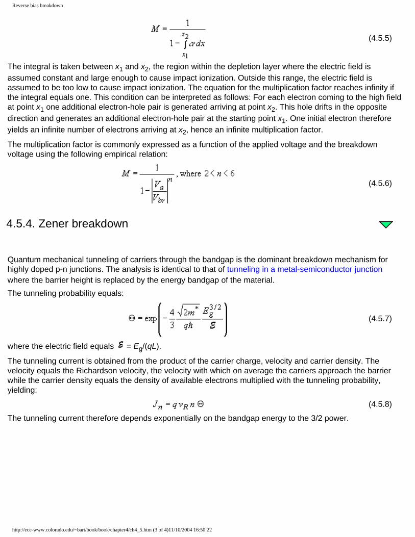
Reverse bias breakdown
(4.5.5)
The integral is taken between x1 and x2, the region within the depletion layer where the electric field is assumed constant and large enough to cause impact ionization. Outside this range, the electric field is assumed to be too low to cause impact ionization. The equation for the multiplication factor reaches infinity if the integral equals one. This condition can be interpreted as follows: For each electron coming to the high field at point x1 one additional electron-hole pair is generated arriving at point x2. This hole drifts in the opposite direction and generates an additional electron-hole pair at the starting point x1. One initial electron therefore yields an infinite number of electrons arriving at x2, hence an infinite multiplication factor.
The multiplication factor is commonly expressed as a function of the applied voltage and the breakdown voltage using the following empirical relation:
(4.5.6)
4.5.4. Zener breakdown
Quantum mechanical tunneling of carriers through the bandgap is the dominant breakdown mechanism for highly doped p-n junctions. The analysis is identical to that of tunneling in a metal-semiconductor junction where the barrier height is replaced by the energy bandgap of the material.The tunneling probability equals:
(4.5.7)
where the electric field equals = Eg/(qL).
The tunneling current is obtained from the product of the carrier charge, velocity and carrier density. The velocity equals the Richardson velocity, the velocity with which on average the carriers approach the barrier while the carrier density equals the density of available electrons multiplied with the tunneling probability, yielding:
(4.5.8)
The tunneling current therefore depends exponentially on the bandgap energy to the 3/2 power.
http://ece-www.colorado.edu/~bart/book/book/chapter4/ch4_5.htm (3 of 4)11/10/2004 16:50:22
Reverse bias breakdown
http://ece-www.colorado.edu/~bart/book/book/chapter4/ch4_5.htm (4 of 4)11/10/2004 16:50:22

Optoelectronic devices
Title Page Table of Contents Help Copyright B. Van Zeghbroeck, 2004
Chapter 4: p-n Junctions
4.6. Optoelectronic devices4.6.1. Photodiodes4.6.2. Solar cells4.6.3. LEDs4.6.4. Laser diodes
P-n junctions are an integral part of several optoelectronic devices. These include photodiodes, solar cells light emitting diodes (LEDs) and semiconductor lasers. In this section we discuss the principle of operation of these devices and derive an expression for key parameters.
4.6.1. Photodiodes
Photodiodes and crystalline solar cells are essentially the same as the p-n diodes, which have been described in this chapter. However, the diode is exposed to light, which yields a photocurrent in addition to the diode current so that the total diode current is given by:
(4.6.1)
where the additional photocurrent, Iph, is due to photogeneration of electrons and holes shown in Figure 4.6.1. These electrons and holes are pulled into the region where they are majority carriers by the electric field in the depletion region.
Figure 4.6.1: Motion of photo-generated carriers in a p-n photodiode.The photo-generated carriers cause a photocurrent, which opposes the diode current under forward bias. Therefore, the diode can be used as a photodetector - using a reverse or zero bias voltage - as the measured photocurrent is proportional to the incident light intensity. The diode can also be used as a solar cell - using a forward bias - to generate electrical power.
http://ece-www.colorado.edu/~bart/book/book/chapter4/ch4_6.htm (1 of 6)11/10/2004 16:50:38
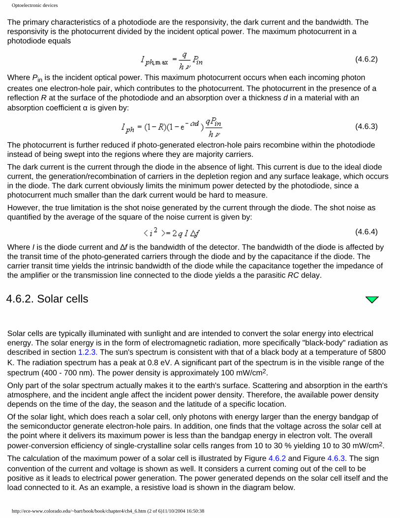
Optoelectronic devices
The primary characteristics of a photodiode are the responsivity, the dark current and the bandwidth. The responsivity is the photocurrent divided by the incident optical power. The maximum photocurrent in a photodiode equals
(4.6.2)
Where Pin is the incident optical power. This maximum photocurrent occurs when each incoming photon creates one electron-hole pair, which contributes to the photocurrent. The photocurrent in the presence of a reflection R at the surface of the photodiode and an absorption over a thickness d in a material with an absorption coefficient α is given by:
(4.6.3)
The photocurrent is further reduced if photo-generated electron-hole pairs recombine within the photodiode instead of being swept into the regions where they are majority carriers. The dark current is the current through the diode in the absence of light. This current is due to the ideal diode current, the generation/recombination of carriers in the depletion region and any surface leakage, which occurs in the diode. The dark current obviously limits the minimum power detected by the photodiode, since a photocurrent much smaller than the dark current would be hard to measure. However, the true limitation is the shot noise generated by the current through the diode. The shot noise as quantified by the average of the square of the noise current is given by:
(4.6.4)
Where I is the diode current and ∆f is the bandwidth of the detector. The bandwidth of the diode is affected by the transit time of the photo-generated carriers through the diode and by the capacitance if the diode. The carrier transit time yields the intrinsic bandwidth of the diode while the capacitance together the impedance of the amplifier or the transmission line connected to the diode yields a the parasitic RC delay.
4.6.2. Solar cells
Solar cells are typically illuminated with sunlight and are intended to convert the solar energy into electrical energy. The solar energy is in the form of electromagnetic radiation, more specifically "black-body" radiation as described in section 1.2.3. The sun's spectrum is consistent with that of a black body at a temperature of 5800 K. The radiation spectrum has a peak at 0.8 eV. A significant part of the spectrum is in the visible range of the spectrum (400 - 700 nm). The power density is approximately 100 mW/cm2. Only part of the solar spectrum actually makes it to the earth's surface. Scattering and absorption in the earth's atmosphere, and the incident angle affect the incident power density. Therefore, the available power density depends on the time of the day, the season and the latitude of a specific location. Of the solar light, which does reach a solar cell, only photons with energy larger than the energy bandgap of the semiconductor generate electron-hole pairs. In addition, one finds that the voltage across the solar cell at the point where it delivers its maximum power is less than the bandgap energy in electron volt. The overall power-conversion efficiency of single-crystalline solar cells ranges from 10 to 30 % yielding 10 to 30 mW/cm2. The calculation of the maximum power of a solar cell is illustrated by Figure 4.6.2 and Figure 4.6.3. The sign convention of the current and voltage is shown as well. It considers a current coming out of the cell to be positive as it leads to electrical power generation. The power generated depends on the solar cell itself and the load connected to it. As an example, a resistive load is shown in the diagram below.
http://ece-www.colorado.edu/~bart/book/book/chapter4/ch4_6.htm (2 of 6)11/10/2004 16:50:38
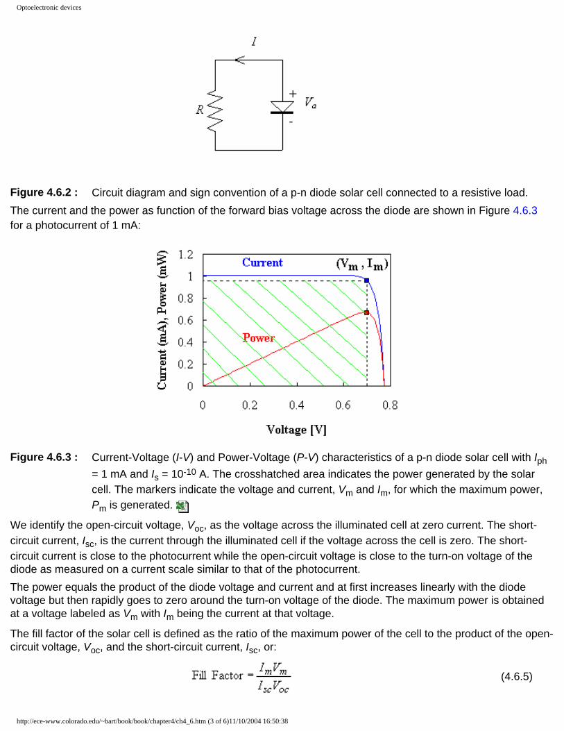
Optoelectronic devices
Figure 4.6.2 : Circuit diagram and sign convention of a p-n diode solar cell connected to a resistive load.The current and the power as function of the forward bias voltage across the diode are shown in Figure 4.6.3 for a photocurrent of 1 mA:
Figure 4.6.3 : Current-Voltage (I-V) and Power-Voltage (P-V) characteristics of a p-n diode solar cell with Iph = 1 mA and Is = 10-10 A. The crosshatched area indicates the power generated by the solar cell. The markers indicate the voltage and current, Vm and Im, for which the maximum power, Pm is generated.
We identify the open-circuit voltage, Voc, as the voltage across the illuminated cell at zero current. The short-circuit current, Isc, is the current through the illuminated cell if the voltage across the cell is zero. The short-circuit current is close to the photocurrent while the open-circuit voltage is close to the turn-on voltage of the diode as measured on a current scale similar to that of the photocurrent. The power equals the product of the diode voltage and current and at first increases linearly with the diode voltage but then rapidly goes to zero around the turn-on voltage of the diode. The maximum power is obtained at a voltage labeled as Vm with Im being the current at that voltage.
The fill factor of the solar cell is defined as the ratio of the maximum power of the cell to the product of the open-circuit voltage, Voc, and the short-circuit current, Isc, or:
(4.6.5)
http://ece-www.colorado.edu/~bart/book/book/chapter4/ch4_6.htm (3 of 6)11/10/2004 16:50:38
Optoelectronic devices
Example 4.6 A 1 cm2 silicon solar cell has a saturation current of 10-12 A and is illuminated with sunlight yielding a short-circuit photocurrent of 25 mA. Calculate the solar cell efficiency and fill factor.
Solution The maximum power is generated for:
where the voltage, Vm, is the voltage corresponding to the maximum power point. This voltage is obtained by solving the following transcendental equation:
Using iteration and a starting value of 0.5 V one obtains the following successive values for Vm:
Vm = 0.5, 0.542, 0.540 V
and the efficiency equals:
The current, Im, corresponding to the voltage, Vm, was calculated using equation (4.6.1) and the power of the sun was assumed 100 mW/cm2. The fill factor equals:
where the open circuit voltage is calculated using equation (4.6.1) and I = 0. The short circuit current equals the photocurrent.
4.6.3. LEDs
Light emitting diodes are p-n diodes in which the recombination of electrons and holes yields a photon. This radiative recombination process occurs primarily in direct bandgap semiconductors where the lowest conduction band minimum and the highest valence band maximum occur at k = 0, where k is the wavenumber. Examples of direct bandgap semiconductors are GaAs, InP, GaP, GaN while most group IV semiconductors including Si, Ge and SiC are indirect bandgap semiconductors.
http://ece-www.colorado.edu/~bart/book/book/chapter4/ch4_6.htm (4 of 6)11/10/2004 16:50:38

Optoelectronic devices
The radiative recombination process is in competition with non-radiative recombination processes such as trap-assisted recombination. Radiative recombination dominates at high minority-carrier densities. Using a quantum well, a thin region with a lower bandgap, positioned at the metallurgical junction, one can obtain high carrier densities at low current densities. These quantum well LEDs have high internal quantum efficiency as almost every electron injected in the quantum well recombines with a hole yielding a photon.The external quantum efficiency of planar LEDs is much lower than unity due to total internal reflection. As the photons are generated in the semiconductor, which has a high refractive index, only photons traveling normal to the semiconductor-air interface can exit the semiconductor. For GaAs with a refractive index of 3.5, the angle for total internal reflection equals 17o so that only a few percent of the generated photons can escape the semiconductor. This effect can be avoided by having a spherical semiconductor shape, which ensures that most photons are normal to the interface. The external quantum efficiency can thereby be increased to values larger than 50%.
4.6.4. Laser diodes
Laser diodes are very similar to LEDs since they also consist of a p-n diode with an active region where electrons and holes recombine resulting in light emission. However, a laser diode also contains an optical cavity where stimulated emission takes place. The laser cavity consists of a waveguide terminated on each end by a mirror. As an example, the structure of an edge-emitting laser diode is shown in Figure 4.6.4. Photons, which are emitted into the waveguide, can travel back and forth in this waveguide provided they are reflected at the mirrors.
Figure 4.6.4 : Structure of an edge-emitting laser diode.The light in the waveguide is amplified by stimulated emission. Stimulated emission is a process where a photon triggers the radiative recombination of an electron and hole thereby creating an additional photon with the same energy and phase as the incident photon. This process is illustrated with Figure 4.6.5. This "cloning" of photons results in a coherent beam.
http://ece-www.colorado.edu/~bart/book/book/chapter4/ch4_6.htm (5 of 6)11/10/2004 16:50:38

Optoelectronic devices
Figure 4.6.5 : Stimulated emission of a photon.The stimulated emission process yields an increase in photons as they travel along the waveguide. Combined with the waveguide losses, stimulated emission yields a net gain per unit length, g. The number of photons can therefore be maintained if the roundtrip amplification in a cavity of length, L, including the partial reflection at the mirrors with reflectivity R1 and R2 equals unity.
This yields the following lasing condition:
(4.6.6)
If the roundtrip amplification is less than one then the number of photons steadily decreases. If the roundtrip amplification is larger than one, the number of photons increases as the photons travel back and forth in the cavity and no steady state value would be obtained. The gain required for lasing therefore equals:
(4.6.7)
Initially, the gain is negative if no current is applied to the laser diode as absorption dominates in the waveguide. As the laser current is increased, the absorption first decreases and the gain increases. The current for which the gain satisfies the lasing condition is the threshold current of the laser, Ith. Below the threshold current very little light is emitted by the laser structure. For an applied current larger than the threshold current, the output power, Pout, increases linearly with the applied current, as each additional incoming electron-hole pair is converted into an additional photon. The output power therefore equals:
(4.6.8)
where hν is the energy per photon. The factor, η, indicates that only a fraction of the generated photons contribute to the output power of the laser as photons are partially lost through the other mirror and throughout the waveguide.
Figure 4.6.6 : Output power from a laser diode versus the applied current.
http://ece-www.colorado.edu/~bart/book/book/chapter4/ch4_6.htm (6 of 6)11/10/2004 16:50:38
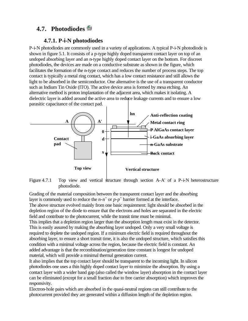
4.7. Photodiodes
4.7.1. P-i-N photodiodes P-i-N photodiodes are commonly used in a variety of applications. A typical P-i-N photodiode is shown in figure 5.1. It consists of a p-type highly doped transparent contact layer on top of an undoped absorbing layer and an n-type highly doped contact layer on the bottom. For discreet photodiodes, the devices are made on a conductive substrate as shown in the figure, which facilitates the formation of the n-type contact and reduces the number of process steps. The top contact is typically a metal ring contact, which has a low contact resistance and still allows the light to be absorbed in the semiconductor. One alternative is the use of a transparent conductor such as Indium Tin Oxide (ITO). The active device area is formed by mesa etching. An alternative method is proton implantation of the adjacent area, which makes it isolating. A dielectric layer is added around the active area to reduce leakage currents and to ensure a low parasitic capacitance of the contact pad.
Top view
A Metal contact ring
Vertical structure
A'
P AlGaAs contact layer
i-GaAs absorbing layer
n-GaAs substrate
Back contact
hν
Contact pad
Anti-reflection coating
0
d
x
Figure 4.7.1 Top view and vertical structure through section A-A' of a P-i-N heterostructure photodiode.
Grading of the material composition between the transparent contact layer and the absorbing layer is commonly used to reduce the n-n+ or p-p+ barrier formed at the interface. The above structure evolved mainly from one basic requirement: light should be absorbed in the depletion region of the diode to ensure that the electrons and holes are separated in the electric field and contribute to the photocurrent, while the transit time must be minimal. This implies that a depletion region larger than the absorption length must exist in the detector. This is easily assured by making the absorbing layer undoped. Only a very small voltage is required to deplete the undoped region. If a minimum electric field is required throughout the absorbing layer, to ensure a short transit time, it is also the undoped structure, which satisfies this condition with a minimal voltage across the region, because the electric field is constant. An added advantage is that the recombination/generation time constant is longest for undoped material, which will provide a minimal thermal generation current. It also implies that the top contact layer should be transparent to the incoming light. In silicon photodiodes one uses a thin highly doped contact layer to minimize the absorption. By using a contact layer with a wider band gap (also called the window layer) absorption in the contact layer can be eliminated (except for a small fraction due to free carrier absorption) which improves the responsivity. Electron-hole pairs which are absorbed in the quasi-neutral regions can still contribute to the photocurrent provided they are generated within a diffusion length of the depletion region.
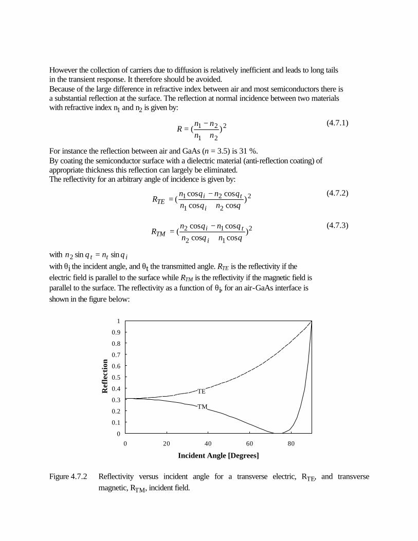
However the collection of carriers due to diffusion is relatively inefficient and leads to long tails in the transient response. It therefore should be avoided. Because of the large difference in refractive index between air and most semiconductors there is a substantial reflection at the surface. The reflection at normal incidence between two materials with refractive index n1 and n2 is given by:
2
21
21 )(nnnn
R+−
= (4.7.1)
For instance the reflection between air and GaAs (n = 3.5) is 31 %. By coating the semiconductor surface with a dielectric material (anti-reflection coating) of appropriate thickness this reflection can largely be eliminated. The reflectivity for an arbitrary angle of incidence is given by:
2
21
21 )coscoscoscos
(θθθθ
nnnn
Ri
tiTE +
−=
(4.7.2)
2
12
12 )coscoscoscos
(θθθθ
nnnn
Ri
tiTM +
−=
(4.7.3)
with itt nn θθ sinsin2 = with θi the incident angle, and θt the transmitted angle. RTE is the reflectivity if the electric field is parallel to the surface while RTM is the reflectivity if the magnetic field is parallel to the surface. The reflectivity as a function of θi, for an air-GaAs interface is shown in the figure below:
Incident Angle [Degrees]
Ref
lect
ion
0
0.1
0.2
0.3
0.4
0.5
0.6
0.7
0.8
0.9
1
0 20 40 60 80
TM
TE
Figure 4.7.2 Reflectivity versus incident angle for a transverse electric, RTE, and transverse
magnetic, RTM, incident field.

4.7.1.1.Responsivity of a P-i-N photodiode
4.7.1.1.1. Generation of electron hole pairs
The generation of electron-hole pairs in a semiconductor is directly related to the absorption of light since every absorbed photon generates one electron-hole pair. The optical generation rate gop is given by1:
ν
α
ν Ah
P
hdx
dP
Ag
optoptop =−=
11
(4.7.4)
where A is the illuminated area of the photodiode, Popt is the incident optical power, α is the absorption coefficient and hν is the photon energy. Note that the optical power is position dependent and obtained by solving:
opt
optP
dx
dPα−=
(4.7.5)
The resulting generation rate must be added to the continuity equation and solved throughout the photodiode which results in the photocurrent.
4.7.1.1.2. Photocurrent due to absorption in the depletion region
Assuming that all the generated electron-hole pairs contribute to the photocurrent, the photocurrent is simply the integral of the generation rate over the depletion region:
∫+
−
−=dx
xopph
n
p
dxgqAI (4.7.6)
where d is the thickness of the undoped region. The minus sign is due to the convention of the positive x direction shown on figure 5.1 . For a P-i-N diode with heavily doped n and p-type region and a transparent top contact layer, this integral reduces to:
)e1(
)1( dinph h
PRqI α
ν−−
−−=
(4.7.7)
where Pin is the incident optical power and R is the reflection at the surface.
4.7.1.1.3. Photocurrent due to absorption in the quasi-neutral region
To find the photocurrent due to absorption in the quasi-neutral region we first have to solve the diffusion equation in the presence of light. For holes in the n-type contact layer this means solving:
)(
1 0 xgpp
dx
J
qdtp
opp
nnpn +−
+∂
−=∂
τ
(4.7.8)
1see section 1.3

Where the electron-hole pair generation gop depends on position. Assuming the n-type contact layer to have the same energy bandgap as the absorption layer, the optical generation rate equals:
να α
AheRP
xgx
inop
−−=
)1()(
(4.7.9)
and the photocurrent due to holes originating in the n-type contact layer equals:
p
npd
p
pd
inph L
pqD
L
L
hPRq
I 0)e1(1
e)1(−−
+−
−= −−
αα
α
α
ν
(4.7.10)
The first term is due to light whereas the second term is the due to thermal generation of electron-hole pairs. This derivation assumes that the thickness of the n-type contact layer is much larger than the diffusion length.
4.7.1.1.4. Absorption in the p-contact region
Even though the contact layer was designed so that no light absorbs in this layer, it will become absorbing at shorter wavelengths. Assuming a worst-case scenario where all the electron-hole pairs, which are generated in the p-type contact layer, recombine without contributing to the photocurrent. The optical power incident on the undoped region is reduced by exp(- α*wp
’) where wp’ is the width of the quasi-neutral p region and α* is the absorption coefficient in
that region.
4.7.1.1.5. Total responsivity:
Combining all the above effects the total responsivity of the detector equals: (ignoring the dark current)
]
1e
1[)exp()1( '*
Lh
waRq
P
I dp
in
ph
αν
α
+−
−−==
−R
(4.7.11)
Note that α*, α and hν are wavelength dependent and given by:
gph EEK −=α and ***
gph EEK −=α (4.7.12)
The quantum efficiency then equals:
]
1e
1)[exp()1( '*L
waRqh d
p αν
ηα
+−−−==
−R
(4.7.13)
4.7.1.1.6. Dark current of the Photodiode:
The dark current of a p-n diode including the ideal diode current, as well as recombination/generation in the depletion region is given by:

)1e(2
)1e)((
2/,'
/2,
00
−+
−++=−−
ta
ta
VV
nr
ui
VVui
n
pn
p
npnip
nxqA
bdnL
nD
L
pDqAI
τ
(4.7.14)
Under reverse bias conditions this expression reduces to:
]
2[ ,
'2,
0
nr
uiui
p
npnip
nxbdn
L
pDqAI
τ++−=−−
(4.7.15)
The ideal diode current due to recombination of electrons has been ignored since np0 = ni,p2/Na is
much smaller than pn0 because the p-layer has a larger band gap. In the undoped region one expects the trap-assisted generation to be much larger than bimolecular generation. Which further reduces the current to:
]
2[ ,
'2,
nr
ui
dp
nipnip
nx
NL
nDqAI
τ+−=−−
(4.7.16)
The trap-assisted recombination tends to dominate for most practical diodes. For photodiodes made with a very pure intrinsic region and/or a narrow band gap, one finds that the dark current depends on thermal generation.
4.7.1.2.Noise in a photodiode
4.7.1.2.1. Shot noise sensitivity
Noise in a p-i-n photodiode is primarily due to shot noise; the random nature of the generation of carriers in the photodiode yields also a random current fluctuation. The square of the current fluctuations equals:
fIqij
j ∆>=< ∑ )(22 (4.7.17)
where Ij are the currents due to different recombination/generation mechanisms and ∆f is the frequency range. Including the ideal diode current, Shockley-Hall-Read and band-to-band recombination as well as generation due to light one obtains:
]
2[2 ,
'2,
0'
02
nr
uiui
p
np
p
pn nxbdn
L
pD
w
nDqAfqi
τ+++∆>=<
)1(2
2/'
RinVV
nr
i PexqAn
ta +++τ
(4.7.18)
The minimum detectable input power depends on the actual signal and the required signal to noise ration. As a first approximation we now calculate the minimum detectable power as the

power, which generates a current equal to the RMS noise current. (A more detailed model for sinusoidal modulated signals is described in section d)
R><
=2
mini
P (4.7.19)
The minimal noise current is obtained at Va = 0 for which the noise current and minimal power equal:
]
222[2
',
2,2 Rin
nr
ui
dp
pni Pxn
NL
Dnfqi ++∆>=<
τ
(4.7.20)
]
222[
2 ',
2,
2min RR
innr
ui
dp
pniP
xn
NL
DnfqP ++
∆=
τ
(4.7.21)
4.7.1.2.2. Equivalence of shot noise and Johnson noise
The following derivation nicely illustrates that shot noise and Johnson noise are not two independent noise mechanisms. In fact we will show that both are the same for the special case of an ideal p-n diode under zero bias. At zero bias the photodetector is also a resistor. Therefore the expression for Johnson noise should apply:
R
fkTi
∆>=<
42 (4.7.22)
The resistance of a photodiode with )1e( / −= ta VVsII is
ta VVs
t
a
I
V
dVdI
R /e
1==
(4.7.23)
or for zero bias the Johnson noise current is given by:
fqI
VfIkT
i st
s ∆=∆
>=< 442
(4.7.24)
whereas the shot noise current at Va = 0 is given by:
fIqeqIi sVV
s ta ∆=+>=< 4)1(2 /2 (4.7.25)
where we added the noise due to the diffusion current to the noise due to the (constant) drift current, since both noise mechanisms do not cancel each other as do the corresponding currents. Equations (4.7.24) and (4.7.25) are identical, thereby proving the equivalence between shot noise and Johnson noise in a photodiode at zero voltage. Note that this relation does not apply if the current is dominated by trap-assisted recombination/generation in the depletion region because of the non-equilibrium nature of the recombination/generation process.
4.7.1.2.3. Examples.
For a diode current of 1µA, a bandwidth ∆f of 1 GHz and a responsivity, R, of 0.2A/W, the noise
current >< 2i equals 18 nA, corresponding to a minimum detectable power of 89 nW or -40.5 dBm. Johnson noise in a 50 Ω resistor, over a bandwidth ∆f of 1 GHz, yields a noise current of 0.58 µA and Pmin = 2.9 µW or -25.4 dBm. If the diode current is only due to the optical power, or I = PminR, then
dBm 58
2min −=
∆=
Rfq
P (4.7.26)
The sensitivity for a given bandwidth can also be expressed as a number of photons per bit:
fh
P∆
=νmintphotons/bi#
(4.7.27)
For instance, for a minimal power of -30 dBm and a bandwidth of 1 GHz, this sensitivity corresponds to 4400 photons per bit.
4.7.1.2.4. Noise equivalent Power and ac noise analysis
Assume the optical power with average value P0 is amplitude modulated with modulation depth, m, as described by:
)e1(0tj
in mPP ω+= (4.7.28)
The ac current (RMS value) in the photodiode with responsivity, R, is then
R
20mP
iph = (4.7.29)
which yields as an equivalent circuit of the photodiode a current source >< 2i in parallel with
a resistance, Req, where Req is the equivalent resistance across the diode and >< 2i is the noise source, which is given by:
)(2 02
eqIRPfIqi +∆=>< (4.7.30)
where the equivalent dark current also includes the Johnson noise of the resistor, Req:
)
2(
eq
tdarkeq R
VII +=
(4.7.31)
The signal to noise ratio is then given by:
)(2 0
220
2
2
2
eqeq
eqph
IRPfqRPm
Ri
Ri
NS
+∆=
><=
(4.7.32)
from the above equation one can find the required optical power P0 needed to obtain a given signal to noise ratio, S/N:

)/(11
2)/(
2
20 NSfq
mI
m
fqNSP
eq
∆++
∆=
R
(4.7.33)
The noise equivalent power is now defined as the ac (RMS) optical power needed to obtain a signal-to-noise ratio of one for a bandwidth of 1 Hz or:
11
2)1/,1(
2NEP
20
q
mI
mq
NSfmP eq
++===∆=R
(4.7.34)
4.7.1.2.5. Optical power limited NEP
for q
mIeq2
<< 1 it is the average optical power rather than the dark current which limits the
NEP.
Rmq22
NEP = (4.7.35)
The noise equivalent power can also be used to calculate the ac optical power if the bandwidth differs from 1Hz from:
f
mP∆= NEP
20
(4.7.36)
where the noise equivalent power has units of W/Hz. However, the optical power is mostly limited by the dark current for which the expressions are derived below.
4.7.1.2.6. Dark current limited NEP
for q
mIeq2
>> 1 it is the dark current (including the Johnson noise of the resistor) which limits
the NEP
R
qIeq2NEP =
(4.7.37)
Again one can use the noise equivalent power to calculate the minimum detectable power for a given bandwidth:
f
mP∆= NEP
20
(4.7.38)
where the noise equivalent power has now units of HzW/ .

4.7.1.3.Switching of a P-i-n photodiode A rigorous solution for the switching time of a P-i-n photodiode starts from the continuity equations for electrons and holes:
),(
12
1
0
2txg
npnnnp
xJ
qtn
opi
in +++
−−
∂∂
=∂∂
τ
(4.7.39)
),(
12
1
0
2txg
npnnnp
x
J
qtp
opi
ip +++
−−
∂
∂−=
∂∂
τ
(4.7.40)
with
xn
qDnqJ pnn ∂∂
+= Eµ (4.7.41)
xp
qDpqJ npp ∂∂
−= Eµ (4.7.42)
and the electric field is obtained from Gauss's law for a P-i-n diode with generation only at t = 0 and neglecting recombination and diffusion these equations reduce to:
Enx
ntn
µ∂∂
=∂∂
and Epxp
tp
µ∂∂
−=∂∂
(4.7.43)
Where the electric field, E, is assumed to be constant and equals:
dVai −
=φ
E (4.7.44)
replacing n(x,t) by n*(x - vnt) and p(x,t) by p*(x - vpt) yields vn = -µnE and vp = µpE the carrier distributions therefore equal those at t = 0 but displaced by a distance µnEt for holes and -µpEt for electrons. The total current due to the moving charge is a displacement current which is given by:
∫∫∫∫ ===d
ph vdxdA
dVdtdx
ddtdQ
tI0
)( ρρ
(4.7.45)
∫ +=d
pnph dxpndA
qtJ0
)()( µµE (4.7.46)
][
)()(
2pn
d
VAqtJ pn
aiph µµ
φ+
−=
(4.7.47)
for t < |d/vn| and t < |d/vp| . For a uniform carrier generation this reduces to:
)]()([
)()( *
0*02
tvdptvdnd
VqAtI ppnn
aiph −+−
−= µµ
φ
(4.7.48)
)]()1([
)()( *
0*0 d
tvdp
d
tvn
dVqA
tIp
pn
nai
ph −+−−
= µµφ
(4.7.49)
In the special case where vn = vp (µn = µp) the full width half maximum (FWHM) of the impulse response is:
2)(2FWHM
2
2r
ainn
tV
d
v
d=
−==
φµ with
)(
2
ainr V
dt
−=
φµ
(4.7.50)
Note: Rule of thumb to convert a pulse response to –3 dB frequency: Assuming the photodiode response to be linear, the FWHM can be related to the half-power frequency by calculating the fourier transform. For a gaussian pulse response (which also yields a gaussian frequency response) this relation becomes
ps)(in FWHM
GHz 440dB3 =−f
(4.7.51)
Since the bandwidth depends on the transit time, which in turn depends on the depletion layer width, there is a tradeoff between the bandwidth and the quantum efficiency.
4.7.1.3.1. Solution in the presence of drift, diffusion and recombination
If we simplify the SHR recombination rate to n/τ and p/τ and assume a constant electric field and initial condition n(x,0) = n0 , the electron concentration can be obtained by solving the continuity equation, yielding:
∑ −−=k
kxx
dxk
Btxn kn πξα sinee),( (4.7.52)
where
]e)1(1[
)()(
222
0 dkk
dk
knB α
απ
π−−
+=
(4.7.53)
with
τ
παξ
1)( 22 ++=
dk
Dnkn and tV2
E=α
(4.7.54)
For this analysis we solved the continuity equation with n(0,t) = n(L,t) = 0 implying infinite recombination at the edges of the depletion region. The initial carrier concentration n0 can also be related to the total energy which is absorbed in the diode at time t = 0:
AdE
En
ph
pulse=0 (4.7.55)

and the photo current (calculated as described above) is
∑ −
−=
kkk
ainph tC
dVqA
tI )exp()(
)( ξφµ
(4.7.56)
with Ck given by
222
20
])()[(
]e)1(1][e)1(1[)(2
πα
π αα
kd
knC
dkdk
k+
−−−−=
−
(4.7.57)
The above equations can be used to calculate the impulse response of a photodiode. Each equation must be applied to electrons as well as holes since both are generated within the diode. Typically electrons and holes have a different mobility, which results in two regions with different slopes. This effect is clearly visible in GaAs diodes as illustrated with the figure below.
Time [s]
Current [A]
0
0.01
0.02
0.03
0.04
0.05
0.06
0.07
0.00E+00 2.00E-11 4.00E-11 6.00E-11 8.00E-11 1.00E-10
jn
jp
j total
Figure 4.7.3 Photocurrent calculated using equation [5.1.50] for a GaAs diode with φi -Va =
0.3 V, Epulse = 10-13 J, Eph = 2 eV and d = 2µm.
4.7.1.3.2. Harmonic solution2 Whereas section b) solves the pulse response one can also solve the frequency response when illuminating with a photon flux Φ1ejωt . (If the photodiode has a linear response, both methods should be equivalent.) To simplify the derivation we assume that the total flux (in photons/s cm2) is absorbed at x = 0. This is for instance the case for a p-i-n diode with a quantum well at the interface between the p-type and intrinsic region and which is illuminated with long wavelength photons, which only absorb in the quantum well. The carriers moving through the depletion region cause a conduction current, Jcond(x):
2See also S.M. Sze "Physics of Semiconductor Devices", Wiley and Sons, second edition p. 756

)/(1)( nvxtj
cond eqxJ −Φ= ω (4.7.58)
where vn = µn E is a constant velocity. From Ampere's law applied to a homogeneous medium:
∫∫∫ ∂
∂+= SdE
tSdJldB s
rrrrrrε
µ0
1
(4.7.59)
we can find the total current as a sum of the conduction and the displacement current:
∫ ∂∂
+=d
scondtotal dxtE
Jd
J0
][1
ε (4.7.60)
if we assume that the electric field is independent of time, the total photo current equals
r
tjtj
ph tjeeq
tJrr
ω
ωω )1()( 1 −Φ
= (4.7.61)
with transit time )(
2
ainr V
dt
−=
φµ. The relative magnitude and phase are shown in the figure
below. (This is a x
xsin function)
from the figure one finds the –3 dB frequency to be:
][
4432
78.23 pst
GHzt
frr
dB ==− π
(4.7.62)
4.7.1.3.3. Time response due to carriers generated in the Q.N. region
For an infinitely long quasi-neutral (Q.N.) region under stationary conditions, the generated carriers are only collected if they are generated within a diffusion length of the depletion region. The average time to diffuse over one diffusion length is the recombination time, τ. Postulating a simple exponential time response we find that the current equals
τ/)0()( tphph eItI −= (4.7.63)
Because of the relatively long carrier lifetime in fast photodiodes, carriers absorbed in the quasi-neutral region produce a long "tail" in the pulse response and should be avoided.
4.7.1.3.4. Dynamic range of a photodiode
The dynamic range is the ratio of the maximal optical power which can be detected to the minimal optical power. In most applications the dynamic range implies that the response is linear as well. The saturation current, defined as the maximum current which can flow through the external circuit, equals:

RV
I aisat
−=
φ
(4.7.64)
which yields an optimistic upper limit for the optical power:
RRV
RI
P aisat −==
φmax
(4.7.65)
and the dynamic range is defined as the ratio of the maximum to the minimum power:
min
max..PP
RD = (4.7.66)
Using [5.1.17] for the minimum power the dynamic range becomes independent of the responsivity and equals:
><
−=
2..
iR
VRD aiφ
(4.7.67)
for example if the equivalent noise current equals Ieq = 1µA, the bandwidth ∆f = 1 GHz, the impedance R = 50 Ω, and the applied voltage Va = 0, then the dynamic range equals 1.35 × 10⁶ (for φi = 1.2 V) or 61.3 dB.
4.7.2. Photoconductors Photoconductors consist of a piece of semiconductor with two ohmic contacts. Under illumination the conductance of the semiconductor changes with the intensity of the incident optical power. The current is mainly due to majority carriers since they are free to flow across the ohmic contacts. However the majority carrier current depends on the presence of the minority carriers. The minority carriers pile up at one of the contacts, where they cause additional injection of majority carriers until the minority carriers recombine. This effect can cause large "photoconductive" gain, which depends primarily of the ratio of the minority carrier lifetime to the majority carrier transit time. Long carrier life times therefore cause large gain, but also a slow response time. The gain bandwidth product of the photoconductor is almost independent of the minority carrier lifetime and depends only on the majority carrier transit time. Consider now a photoconductor with length, L, width W and thickness d, which is illuminated a total power, P. The optical power, P(x), in the material decreases with distance due to absorption and is described by:
)(
)(xP
dxxdP
α−= , yielding )exp()0()( xPxP α−= (4.7.68)
The optical power causes a generation of electrons and holes in the material. Solving the diffusion equation [5.1.7] for the steady state case and in the absence of a current density gradient one obtains for the excess carrier densities:
WLh
xPpn
ναατ )exp()0('' −
== (4.7.69)
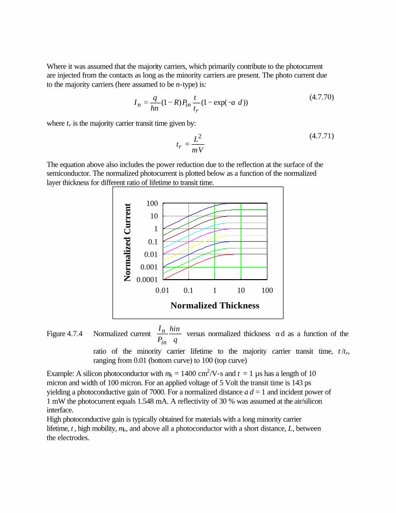
Where it was assumed that the majority carriers, which primarily contribute to the photocurrent are injected from the contacts as long as the minority carriers are present. The photo current due to the majority carriers (here assumed to be n-type) is:
))exp(1()1( d
tPR
hq
Ir
inn ατ
ν−−−=
(4.7.70)
where tr is the majority carrier transit time given by:
VL
tr µ
2=
(4.7.71)
The equation above also includes the power reduction due to the reflection at the surface of the semiconductor. The normalized photocurrent is plotted below as a function of the normalized layer thickness for different ratio of lifetime to transit time.
Normalized Thickness
Nor
mal
ized
Cur
rent
0.0001
0.001
0.01
0.1
1
10
100
0.01 0.1 1 10 100
Figure 4.7.4 Normalized current q
hPI
in
n ιν versus normalized thickness αd as a function of the
ratio of the minority carrier lifetime to the majority carrier transit time, τ/tr, ranging from 0.01 (bottom curve) to 100 (top curve)
Example: A silicon photoconductor with µn = 1400 cm2/V-s and τ = 1 µs has a length of 10 micron and width of 100 micron. For an applied voltage of 5 Volt the transit time is 143 ps yielding a photoconductive gain of 7000. For a normalized distance αd = 1 and incident power of 1 mW the photocurrent equals 1.548 mA. A reflectivity of 30 % was assumed at the air/silicon interface. High photoconductive gain is typically obtained for materials with a long minority carrier lifetime, τ, high mobility, µn, and above all a photoconductor with a short distance, L, between the electrodes.
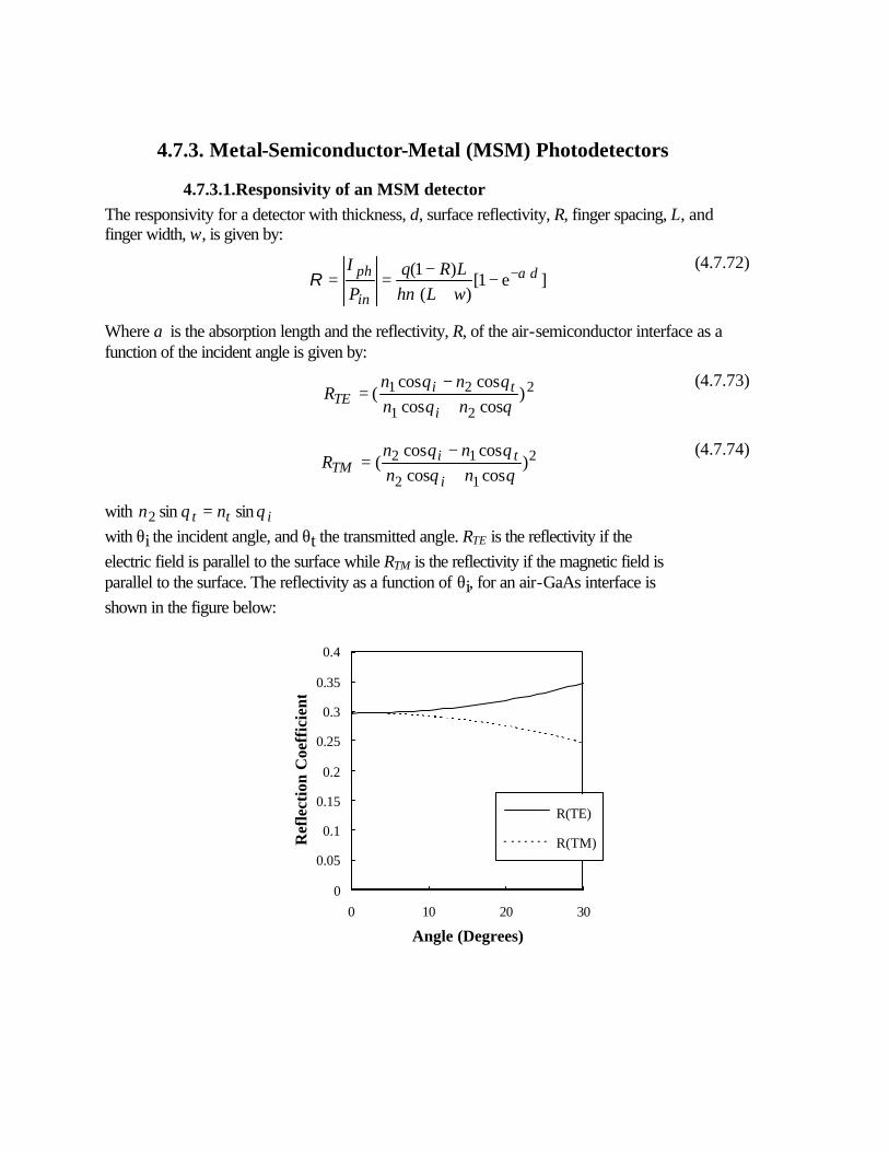
4.7.3. Metal-Semiconductor-Metal (MSM) Photodetectors
4.7.3.1.Responsivity of an MSM detector The responsivity for a detector with thickness, d, surface reflectivity, R, finger spacing, L, and finger width, w, is given by:
]e1[
)()1( d
in
ph
wLhLRq
P
I αν
−−+
−==R
(4.7.72)
Where α is the absorption length and the reflectivity, R, of the air-semiconductor interface as a function of the incident angle is given by:
2
21
21 )coscoscoscos
(θθθθ
nnnn
Ri
tiTE +
−=
(4.7.73)
2
12
12 )coscoscoscos
(θθθθ
nnnn
Ri
tiTM +
−=
(4.7.74)
with itt nn θθ sinsin2 = with θi the incident angle, and θt the transmitted angle. RTE is the reflectivity if the electric field is parallel to the surface while RTM is the reflectivity if the magnetic field is parallel to the surface. The reflectivity as a function of θi, for an air-GaAs interface is shown in the figure below:
Angle (Degrees)
Ref
lect
ion
Coe
ffic
ient
0
0.05
0.1
0.15
0.2
0.25
0.3
0.35
0.4
0 10 20 30
R(TE)
R(TM)

Incident Angle [Degrees]
Ref
lect
ion
0
0.1
0.2
0.3
0.4
0.5
0.6
0.7
0.8
0.9
1
0 50 100 150
TM
TE
Figure 4.7.5 Angular dependencies of the reflectivity of an Air-to-GaAs interface
Including drift, diffusion and recombination the responsivity becomes:
t
ad
in
ph
VV
wLhLRq
P
I]e1[
)()1( α
ν−−
+−
==R (4.7.75)
)(csche)coth(1(
)(21e
[)(
3
2LLL
L
Ln
Ln
n
Ln n
ββαβ
ααβ
+−−
−−×
−
(4.7.76)
)](csche)coth(1(
)(21e )(
LL nL
nn
Lnββ
βαα
βα−+
+−
++−
(4.7.77)
)(csche)coth(1(
)(21e
[)(
3
2
LLLL
Lp
Lp
p
Lp p
ββαβ
ααβ
+−−
−−
−
(4.7.78)
)](csche)coth(1(
)(21e )(
LL pL
pp
Lpββ
βαα
βα−+
+−
++−
(4.7.79)
with
LVV
t
a2
=α . 22 1
nn
L+= αβ and
22 1
pp
L+= αβ
(4.7.80)
The above expression can be used to calculate the current as a function of the applied voltage. An example is shown below. Both the electron and the hole current are plotted as is the total

current. The difference between the electron and hole current is due to the recombination of carriers. For large voltages all carriers generated are swept out yielding a saturation of the photocurrent with applied voltage, whereas for small voltages around zero diffusion is found to be the dominant mechanism. Around zero volts it is the ratio of the transit time to the diffusion time, which determines the current. In the absence of velocity saturation both times depend on the carrier mobility so that the ratio becomes independent of the carrier mobility. This causes the I-V curves to be identical for electrons and holes in the absence of recombination.
Voltage [V]
Cur
rent
[mA
]
0
0.1
0.2
0.3
0.4
0.5
0.6
0.7
0 0.5 1 1.5 2
I total
In
Ip
Figure 4.7.6 Current - Voltage characteristic of an MSM photodiode.
4.7.3.2.Pulse response of an MSM detector The pulse response can be calculated by solving the time dependent continuity equation, yielding:
∑ −−− +−
+−
=k
tp
tnk
daph
kpknCwL
LRL
qAVtI ]ee[]e1[
)1()(
ξξα µµ (4.7.81)
with Ck given by:
222
20
])()[(
]e)1(1][e)1(1[)(2
πα
π αα
kd
knC
dkdk
k+
−−−−=
−
(4.7.82)
where
ALE
En
ph
pulse=0 (4.7.83)
and

τ
παξ
1)( 22 ++=
dk
Dnkn , τ
παξ
1)( 22 ++=
dk
Dpkp and
tV2E
=α
(4.7.84)
Time [s]
Cur
rent
[A]
0
0.01
0.02
0.03
0.04
0.05
0.06
0.07
0.00E+00 5.00E-11 1.00E-10
In
Ip
Itotal
Figure 4.7.7 Transient behavior (Pulse energy, Epulse = 0.1 pJ, Va = 0.3V)
4.7.3.3.Equivalent circuit of an MSM detector. The equivalent circuit of the diode consists of the diode capacitance, Cp, a parallel resistance, Rp, obtained from the slope of the I-V characteristics at the operating voltage in parallel to the photocurrent, Iph, which is obtained by calculating the convolution of the impulse response and the optical input signal. A parasitic series inductance, LB, primarily due to the bond wire, and a series resistance, Rs, are added to complete the equivalent circuit.
RCIph pp
R sL B
Figure 4.7.8 Equivalent circuit of an MSM detector
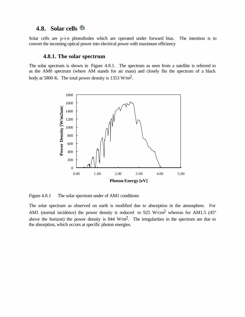
4.8. Solar cells Solar cells are p-i-n photodiodes which are operated under forward bias. The intention is to convert the incoming optical power into electrical power with maximum efficiency
4.8.1. The solar spectrum
The solar spectrum is shown in Figure 4.8.1. The spectrum as seen from a satellite is referred to as the AM0 spectrum (where AM stands for air mass) and closely fits the spectrum of a black body at 5800 K. The total power density is 1353 W/m2.
Photon Energy [eV]
Pow
er D
ensi
ty [W
/m2u
m]
0
200
400
600
800
1000
1200
1400
1600
1800
0.00 1.00 2.00 3.00 4.00 5.00
Figure 4.8.1 The solar spectrum under of AM1 conditions
The solar spectrum as observed on earth is modified due to absorption in the atmosphere. For AM1 (normal incidence) the power density is reduced to 925 W/cm2 whereas for AM1.5 (45° above the horizon) the power density is 844 W/m2. The irregularities in the spectrum are due to the absorption, which occurs at specific photon energies.
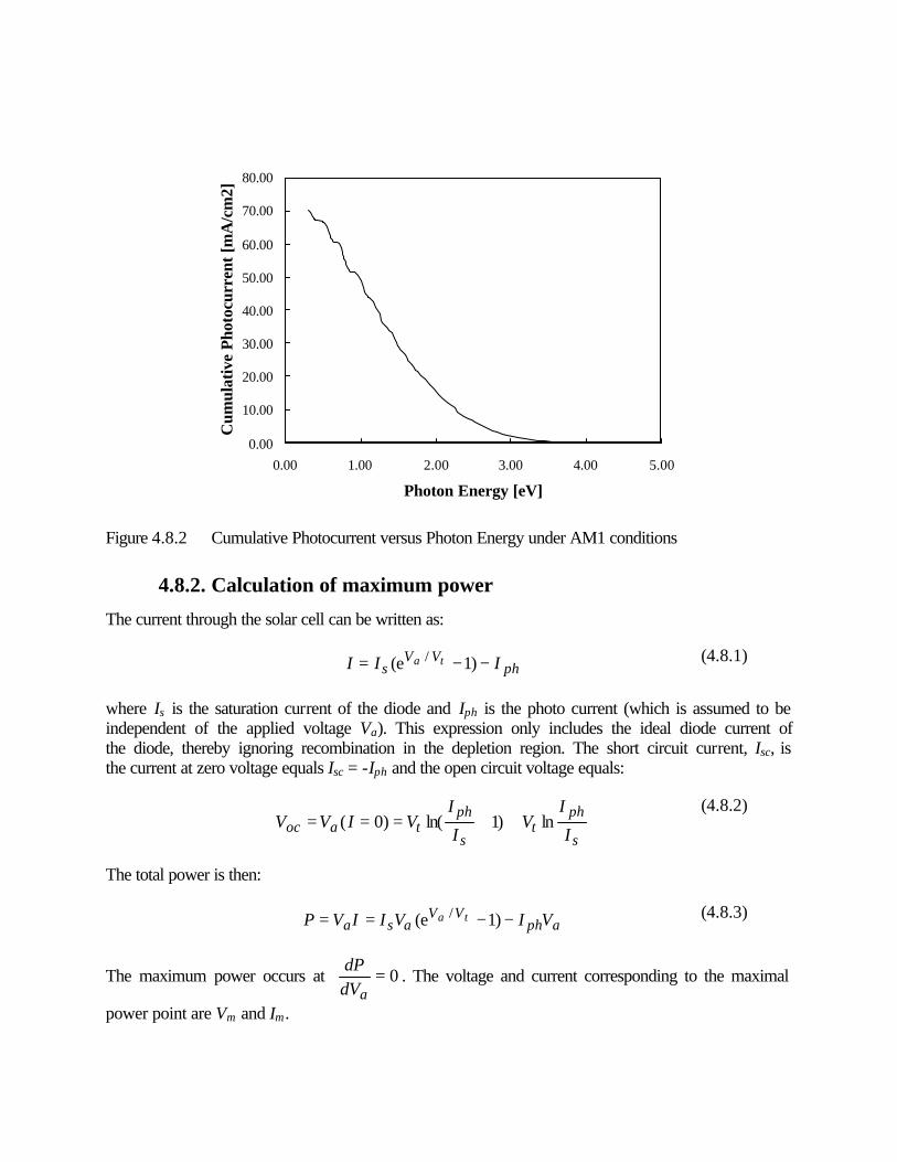
Photon Energy [eV]
Cum
ulat
ive
Phot
ocur
rent
[mA
/cm
2]
0.00
10.00
20.00
30.00
40.00
50.00
60.00
70.00
80.00
0.00 1.00 2.00 3.00 4.00 5.00
Figure 4.8.2 Cumulative Photocurrent versus Photon Energy under AM1 conditions
4.8.2. Calculation of maximum power
The current through the solar cell can be written as:
ph
VVs III ta −−= )1e( / (4.8.1)
where Is is the saturation current of the diode and Iph is the photo current (which is assumed to be independent of the applied voltage Va). This expression only includes the ideal diode current of the diode, thereby ignoring recombination in the depletion region. The short circuit current, Isc, is the current at zero voltage equals Isc = -Iph and the open circuit voltage equals:
s
pht
s
phtaoc I
IV
I
IVIVV ln)1ln()0( ≅+===
(4.8.2)
The total power is then:
aph
VVasa VIVIIVP ta −−== )1e( / (4.8.3)
The maximum power occurs at 0=adV
dP. The voltage and current corresponding to the maximal
power point are Vm and Im.

tmtm VV
t
msph
VVs
a VVI
IIdVdP // e)1e(0 +−−==
(4.8.4)
This equation can be rewritten as:
)]1ln([]
1
1ln[
t
m
t
oct
t
ms
sphtm
V
V
V
VV
V
VI
IIVV +−≅
+
+=
(4.8.5)
Using equation [5.3.2] for the open circuit voltage Voc. The most accurate solution is obtained by solving this transcendental equation and substituting into equations [5.3.1] and [5.3.3]. The maximum power can be approximated by:
))1ln()(1(
t
mtoc
m
tphmmm V
VVV
VV
IVIP +−−−≅= (4.8.6)
))1ln((
m
toc
t
mtocphm V
VVVV
VVIP −+−−≅ (4.8.7)
or
qE
IP mphm −=
(4.8.8)
where
))1ln((
m
toc
t
mtocm V
VVVV
VVqE −+−= (4.8.9)
The energy Em is the energy of one photon, which is converted to electrical energy at the maximum power point. The total photo current is calculated as (for a given bandgap Eg)
qEJ gph =)( (4.8.10)
and the efficiency equals:
in
mph
in
mqP
EI
PP
==η (4.8.11)

4.8.3. Conversion efficiency for monochromatic illumination
This first order model provides an analytic approximation for the efficiency of a solar cell under monochromatic illumination. Starting from the result of the previous paragraph:
))1ln((
m
toc
t
mtoc
in
ph
in
mV
VVVV
VVP
I
PP
−+−==η (4.8.12)
We replace Voc by the largest possible open circuit voltage, q
Eg , yielding:
)1ln(
kT
EV
q
EV g
tg
m +−= (4.8.13)
and
)]1ln(
21[
kT
E
EkT
P
VI g
gin
mph +−==η (4.8.14)
for a GaAs solar cell at 300K, q
Eg = 55 so that the efficiency equals η = 85%
4.8.4. Effect of diffusion and recombination in a solar cell
4.8.4.1.Photo current versus voltage
The photo current is obtained by first solving the continuity equation for electrons
opnn g
ndxdn
dx
ndD +−+=
τµ E
2
20
(4.8.15)
as well as a similar equation for holes. The photo current is obtained from
∫ +−=d
pnaiaph dxpnVd
qAVI
02 )()()( µµφ
(4.8.16)
Once this photocurrent is obtained the total current is obtained from:
)()1e( /aph
VVs VIII ta −−= (4.8.17)
To obtain the corresponding maximum power one has to repeat the derivation of section 5.3.2.
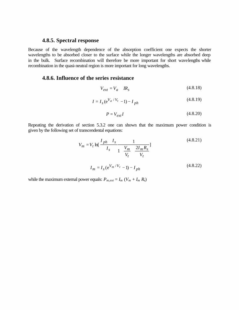
4.8.5. Spectral response
Because of the wavelength dependence of the absorption coefficient one expects the shorter wavelengths to be absorbed closer to the surface while the longer wavelengths are absorbed deep in the bulk. Surface recombination will therefore be more important for short wavelengths while recombination in the quasi-neutral region is more important for long wavelengths.
4.8.6. Influence of the series resistance
saext IRVV += (4.8.18)
ph
VVs III ta −−= )1e( / (4.8.19)
IVP ext= (4.8.20)
Repeating the derivation of section 5.3.2 one can shown that the maximum power condition is given by the following set of transcendental equations:
]
21
1ln[
t
sm
t
ms
sphtm
VRI
VVI
IIVV
++
+=
(4.8.21)
ph
VVsm III tm −−= )1e( / (4.8.22)
while the maximum external power equals: Pm,ext = Im (Vm + Im Rs)

4.9. LEDs A light emitting diode consists of a p-n diode, which is designed so that radiative recombination dominates. Homojunction p-n diodes, heterojunction p-i-n diodes where the intrinsic layer has a smaller bandgap (this structure is also referred to as a double-hetero-structure) and p-n diodes with a quantum well in the middle are all used for LEDs. We will only consider the p-n diode with a quantum well because the analytical analysis is more straightforward and also since this structure is used often in LEDs and even more frequently in laser diodes.
4.9.1. Rate equations
The LED rate equations are derived from the continuity equations as applied to the p-n diode:
GR
xJ
qtn n +−
∂∂
=∂∂ 1
(4.9.1)
where G is the generation rate per unit volume and R is the recombination rate per unit volume. This equation is now simplified by integrating in the direction perpendicular to the plane of the junction. We separate the integral in two parts: one for the quantum well, one for the rest of the structure.
nri
i
kkikkk
idealbbSHR
NPNNNP
BNPNq
Jq
Jq
JqJ
tn
tn
τ1
2)(
1
212
n-pqw ++−
−−−−−−=∂∂
+∂∂ ∑∫∫ (4.9.2)
where k refers to the quantum number in the well. If we ignore the carriers everywhere except in the quantum well and assume that only the first quantum level is populated with electrons/holes and that the density of electrons equals the density of holes, we obtain:
abnr
SNNB
qJ
tN
ττ+−−=
∂∂
22
1 (4.9.3)
where the last term is added to include reabsorption of photons. The rate equation for the photon density including loss of photons due to emission (as described with the photon lifetime τph) and absorption (as described with the photon absorption time τab) equals:
abph
SSNB
tS
ττ+−=
∂∂ 2
1 (4.9.4)
The corresponding voltage across the diode equals:
)]1)(1ln[( *//, −−+= Vc NNNN
tqwg
a eeVq
EV
(4.9.5)
Where the modified effective hole density of states in the quantum well, Nv*, accounts for the occupation of multiple hole levels as described in section 4.4.3.d. The optical output power is given by the number of photons, which leave the semiconductor per unit time, multiplied with the photon energy:

4)1(
2c
phout RA
ShP
Θ−=
τν
(4.9.6)
where A is the active area of the device, R is the reflectivity at the surface and Θc is the critical angle for total internal reflection1
)(sin and )(
2
112
21
21
nn
nnnn
R c−=Θ
+−
= (4.9.7)
The reflectivity and critical angle for a GaAs Air interface are 30 % and 16º respectively.
4.9.2. DC solution to the rate equations
The time independent solution in the absence of reabsorption, as indicated with the subscript 0, is obtained from:
ph
NBN
qJ
τ20 02
00 −−=
(4.9.8)
ph
SBN
τ02
00 −= (4.9.9)
where B is the bimolecular recombination constant. Solving these equations yields:
]1
161[
41 0
2
0 −+=q
BJB
N nr
nr
ττ
(4.9.10)
for small currents this reduces to: (J << q/16τnr2B)
qJ
N nr 00
2τ=
(4.9.11)
which indicates that SHR recombination dominates, whereas for large currents one finds: (J >> q/16τnr
2B)
qBJ
N 00 =
(4.9.12)
The DC optical output power is:
1See Appendix A.7 for the derivation of the reflectivity at dielectric interfaces.

)1(200 RABNhP −= ν (4.9.13)
This expression explains the poor efficiency of an LED. Even if no non-radiative recombination occurs in the active region of the LED, most photons are confined to the semiconductor because of the small critical angle. Typically only a few percent of the photons generated escape the semiconductor. This problem is most severe for planar surface emitting LEDs. Better efficiencies have been obtained for edge emitting, "superluminescent" LEDs (where stimulated emission provides a larger fraction of photons which can escape the semiconductor) and LEDs with curved surfaces.
4.9.3. AC solution to the rate equations
Assume that all variables can be written as a sum of a time independent term and a time dependent term (note that n(t) is still a density per unit area):
)(10 tnNN += )(10 tjJJ += (4.9.14)
)(10 tsSS += )(10 tpPP += (4.9.15)
)(0, tvVV aaa += (4.9.16)
The rate equations for the time dependent terms the given by:
qtjtn
tBntnNBt
n )(2
)()()(2 1
0
12110
1 +−−−=∂∂
τ
(4.9.17)
Needs beta ??
ph
tstBntnNB
ts
τ)(
)()(2 12110
1 −+=∂∂
(4.9.18)
Assuming the AC current of the form j1 = j1,0ejωt and ignoring the higher order terms we can obtain a harmonic solution of the form:
tjnn ωe0,11 = tjss ωe0,11 = tjpp ωe0,11 = (4.9.19)
yielding:
)1)(1(
21 0,100,1
effph
effph
jj
jNB
qs
ωτωτ
ττ
++=
(4.9.20)
where τeff depends on N0 as:
00 2
12
1
τ
τ+
=BN
eff (4.9.21)
and the AC responsivity is:
)1)(1(
2
4)1( 0
2
0,1
0,1
effph
effcjj
NBR
qh
j
p
τωτω
τ
ππν
++Θ
−= (4.9.22)
at ω = 0 this also yields the differential quantum efficiency (D.Q.E)
14)1(
2
)1(D.Q.E.
00
0020
2
0,1
0,1
+Θ−
=Θ−
==τ
ττ
ν BNBNRBNR
hq
j
p ceffc (4.9.23)
4.9.4. Equivalent circuit of an LED
The equivalent circuit of an LED consists of the p-n diode current source parallel to the diode capacitance and in series with a linear series resistance, R. The capacitance, C, is obtained from:
qdNdV
dQdV
Caa ==
1
(4.9.24)
)1e)(1e(
)]1(1
)1(1
[11
//
////
−−
−+−=
vc
cvvc
NNNN
NNNN
v
NNNN
ct
eeN
eeN
VqC
(4.9.25)
or
tmVqN
C 0= (4.9.26)
with
)1()1( /
/0
/
/0
−+
−=
v
v
c
c
NNv
NN
NNc
NN
eN
eN
eN
eNm
(4.9.27)
for N0 << Nc and/or Nv, m = 2 while for N0 >> Nc and/or Nv, vc
vcNN
NNNm
)(0 +=

4.10. Laser diodes
4.10.1. Emission, Absorption and modal gain
The analysis of a semiconductor laser diode requires a detailed knowledge of the modal gain, which quantifies the amplification of light confined to the lasing mode. To find the modal gain, one starts from the notion that the emission as well as absorption of photons, requires the conservation of energy and momentum of all particles involved in the process. The conservation of energy requires that the photon energy equals the difference between the electron and hole energy:
pnph EEE −= (4.10.1)
with
*
22
1 2 n
nncn m
kEEE
h++=
(4.10.2)
*
22
1 2 p
ppvp m
kEEE
h+−=
(4.10.3)
The conservation of momentum requires that the electron momentum equals that of the empty state it occupies in the valence band plus the momentum of the photon:
phpn kkk += (4.10.4)
The photon momentum is much smaller than that of the electron and hole, so that the electron and hole momentum are approximately equal. As a result we can replace kn and kp by a single variable k. Equations (4.10.1), (4.10.2), (4.10.3) and (4.10.4) then result in:
*
22
1, 2 rqwgph m
kEE
h+=
(4.10.5)
where Eg,qw1 is the energy between the lowest electron energy in the conduction band and the lowest hole energy in the valence band. mr
* is the reduced effective mass given by:
***
111
pnr mmm+=
(4.10.6)
The electron and hole energies, En and Ep, can then be expressed as a function of the photon energy by:
*
*
1,1 )(n
rqwgphncn m
mEEEEE −++=
(4.10.7)

*
*
1,1 )(p
rqwgphpvp m
mEEEEE −−−=
(4.10.8)
The emission and absorption spectra (β(Eph) and α(Eph)) of a quantum well depend on the density of states and the occupancy of the relevant states in the conduction and valence band. Since the density of states in the conduction and valence band are constant in a quantum well, the emission and absorption can be expressed as a product of a maximum emission and absorption rate and the probability of occupancy of the conduction and valence band states, namely:
[ ])(1)()( max ppnnph EfEfE −= ββ (4.10.9)
[ ] )()(1)( max ppnnph EfEfE −= αα (4.10.10)
Stimulated emission occurs if an incoming photon triggers the emission of another photon. The net gain in the semiconductor is the stimulated emission minus the absorption. The maximum stimulated emission equals the maximum absorption since the initial and final states are simply reversed so that the transition rates as calculated based on the matrix elements are the same. The net gain is then given by:
)]()([)()()( max ppnnphphph EfEfgEEEg −=−= αβ (4.10.11)
where the maximum stimulated emission and the maximum absorption were replaced by the maximum gain, gmax. The normalized gain spectrum is shown in Figure 4.10.1 for different values of the carrier density. The two staircase curves indicate the maximum possible gain and the maximum possible absorption in the quantum well.
Photon Energy [eV]
Ise/
Ise,
max
1
-2.5
-2
-1.5
-1
-0.5
0
0.5
1
1.5
2
2.5
1.4 1.45 1.5 1.55 1.6 1.65 1.7 1.75 1.8 1.85 1.9
Figure 4.10.1 Normalized gain versus photon energy of a 10nm GaAs quantum well for a carrier density of 1012 (lower curve), 3 x 10¹², 5 x 10¹², 7 x 10¹² and 9 x 10¹²
(upper curve) cm-2.
The theoretical gain curve of Figure 4.10.1 exhibits a sharp discontinuity at Eph = Eg,qw1. The gain can also be expressed as a function of the carrier densities, N and P, when assuming that only one electron and one hole level is occupied:
−+−
−−
−
−
−
−−+
−−
=
)exp()exp())exp(1(
)exp(
1)exp()exp(1
)exp(1
)(
,*
*1,
,
,
*
*1,
,
,
max
qwvp
rphqwg
qwv
qwv
n
rqwgph
qwc
qwc
ph
NP
mm
kT
EE
NP
NP
mm
kTEE
NN
NN
gEg
(4.10.12)
The peak value at Eph = Eg,qw1, assuming quasi-neutrality (N = P) is then:
( )vc NNNNqwgpeak egEgg //
max1, e1)( −− −−== (4.10.13)
The maximum gain can be obtained from the absorption of light in bulk material since the wavefunction of a free electron in bulk material is the same as the wavefunction in an infinite stack of infinitely deep quantum wells, provided the barriers are infinitely thin and placed at the nodes of the bulk wavefunction. This means that for such a set of quantum wells the absorption would be the same as in bulk provided that the density of states is also the same. This is the case for Eph = Eqw1 so that the maximum gain per unit length is given by:
xrqw Lm
hKEEKg
122 *
2
11max =−= (4.10.14)
where Lx is the width of the quantum well. This expression shows that the total gain of a single quantum well due to a single quantized level is independent of the width1. The corresponding value for GaAs quantum wells is 0.006 or 0.6%.
Experimental gain curves do not show the discontinuity at Eph = Eqw1 due to inter-carrier scattering which limits the lifetime of carriers in a specific state. The line width of a single set of electron and hole levels widens as a function of the scattering time, which disturbs the phase of the atomic oscillator. Therefore, an approximation to the actual gain curve can be obtained by convoluting (6.2.10) with a Lorenzian line shape function:
1There is a weak dependence of m* on the width of the well.

∫ ∆
+−
∆−= ν
ννπ
νd
h
EEFEFgEg
phppnnph
])2
()[(2)]()([)(
22max
(4.10.15)
with τπ
ν11
=∆ , where τ is the carrier collision time in the quantum well. The original and
convoluted gain curves are shown in Figure 4.10.2.
Photon Energy [eV]
Ise/
Ise,
max
1
-2.5
-2
-1.5
-1
-0.5
0
0.5
1
1.5
2
2.5
1.4 1.6 1.8 2 2.2 2.4
Figure 4.10.2 Original and convoluted gain spectrum of a 10 nm GaAs quantum well with a carrier density of 3 x 1012 cm-2 and a collision time of 0.09 ps.
For lasers with long cavities such as edge-emitter lasers, one finds that the longitudinal modes are closely spaced so that lasing will occur at or close to the peak of the gain spectrum. It is therefore of interest to find an expression for the peak gain as a function of the carrier density2. A numeric solution is shown in Figure 4.10.3 where the peak gain is normalized to the maximum value of the first quantized energy level. Initially, the gain peak is linear with carrier concentration but saturates because of the constant density of states, until the gain peak associated with the second quantized level takes over. Since the peak gain will be relevant for lasing we will consider it more closely. As a first order approximation we will set the peak gain
2Experimental values for the gain versus current density can be found in: G. Hunziker, W. Knop and C. Harder, "Gain Measurements on One, Two and Three Strained GaInP Quantum Well Laser Diodes", IEEE Trans. Quantum Electr., Vol. 30, p 2235-2238, 1994.
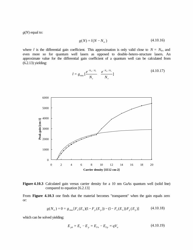
g(N) equal to:
)()( trNNNg −= l (4.10.16)
where l is the differential gain coefficient. This approximation is only valid close to N = Ntr, and even more so for quantum well lasers as opposed to double-hetero-structure lasers. An approximate value for the differential gain coefficient of a quantum well can be calculated from (6.2.13) yielding:
][
//
maxv
NN
c
NN
Ne
Ne
gvtrctr −−
+=l (4.10.17)
Carrier density [1E12 cm-2]
Peak
gai
n [c
m-1
]
0
1000
2000
3000
4000
5000
6000
0 2 4 6 8 10 12 14 16 18 20
Figure 4.10.3 Calculated gain versus carrier density for a 10 nm GaAs quantum well (solid line) compared to equation [6.2.13]
From Figure 4.10.3 one finds that the material becomes "transparent" when the gain equals zero or:
)]())(1())(1)(([0)( max ppnnppnntr EFEFEFEFgNg −−−== (4.10.18)
which can be solved yielding:
aFpFnpnph qVEEEEE =−=−= (4.10.19)

The transparency current density is defined as the minimal current density for which the material becomes transparent for any photon energy larger than or equal to Eg,qw1. This means that the
transparency condition is fulfilled for q
EV qwg
a1.= . The corresponding carrier density is referred
to as Ntr, the transparency carrier density. The transparency carrier density can be obtained from by setting gmax = 0, yielding
)1ln( / vtr NNctr eNN −−= (4.10.20)
This expression can be solved by iteration for Nv > Nc. The solution is shown in Figure 4.10.4.
Nv/Nc
Ntr
/Nc
0
0.5
1
1.5
2
2.5
0 5 10 15 20
Figure 4.10.4 Normalized transparency carrier density versus the ratio of the effective density of states in the valence and conduction band.
To include multiple hole levels one simply replaces Nv by Nv* as described in section 4.4.3.d.
4.10.2. Principle of operation of a laser diode
A laser diode consists of a cavity, defined as the region between two mirrors with reflectivity R1 and R2, and a gain medium, in our case a quantum well. The optical mode originates in spontaneous emission, which is confined to the cavity by the waveguide. This optical mode is amplified by the gain medium and partially reflected by the mirrors. The modal gain depends on the gain of the medium, multiplied with the overlap between the gain medium and the optical mode which we call the confinement factor, Γ, or:
Γ= )(gain modal Ng (4.10.21)

This confinement factor will be calculated in section 6.2.5. Lasing occurs when for light traveling round trip through the cavity the optical gain equals the losses. For a laser with modal gain g(N)Γ and wave guide loss α this condition implies:
1]))((2exp[21 =− LNgRR α (4.10.22)
where L is the length of the cavity. The distributed loss of the mirrors is therefore:
21
1ln
1lossmirror
RRL=
(4.10.23)
4.10.3. Longitudinal modes in the laser cavity.
Longitudinal modes in the laser cavity correspond to standing waves between the mirrors. If we assume total reflection at the mirrors this wave contains N/2 periods where N is an integer. For a given wave length λ and a corresponding effective index, neff, this yields:
λ
LnN eff2
= (4.10.24)
Because of dispersion in the waveguide, a second order model should also include the wavelength dependence of the effective index. Ignoring dispersion we find the difference in wavelength between two adjacent longitudinal modes from:
1
2
λ
LnN eff=
(4.10.25)
2
21
λ
LnN eff=+
(4.10.26)
effeff LnNN
Ln2
)1
11(2
21λ
λ ≅+
−=∆ (4.10.27)
Longer cavities therefore have closer spaced longitudinal modes. An edge emitting (long) cavity with length of 300 µm, neff = 3.3, and λ = 0.8 µm has a wavelength spacing ∆λ of 0.32 nm while a surface emitting (short) cavity of 3 µm has a wavelength spacing of only 32 nm. These wavelength differences can be converted to energy differences using:
22 λλ∆
==∆ pheff
ELnhc
E (4.10.28)
so that 0.32 nm corresponds to -6.2 meV and 32 nm to 620 meV. A typical width of the optical gain spectrum is 60 meV, so that an edge emitter biased below threshold can easily contain 10 longitudinal modes, while for a surface emitter the cavity must be carefully designed so that the

longitudinal mode overlaps with the gain spectrum.
A more detailed analysis of a Fabry-Perot etalon is described in A.7.3, providing the reflectivity, absorption and transmission as a function of photon energy.
4.10.4. Waveguide modes3
The optical modes in the waveguide determine the effective index used to calculate the longitudinal modes as well as the confinement factor which affects the modal gain. Starting from Maxwell's equations in the absence of sources:
),,(20 zyxnH ε=×∇
rr (4.10.29)
tH∂
∂=×∇
rrr
0µE (4.10.30)
and assuming a propagating wave in the z-direction and no variation in the y-direction we obtain the following one-dimensional reduced wave equation for a time harmonic field, E = Ex ejωt, of a TM mode:
0))(( 222
2
2=−+ x
x kxndx
dE
Eβ
(4.10.31)
with the propagation constant given by effncω
β = , and c
kω
= , this equation becomes:
0))(( 22
2
2=−+ xeff
x nxndx
dE
E
(4.10.32)
this equation is very similar to the Schrödinger equation. In fact previous solutions for quantum wells can be used to solve Maxwell's equation by setting the potential V(x) equal to -n2 (x) and
replacing 2
2
c
ω by
2
*2
h
m. The energy eigenvalues, El, can then be interpreted as minus the
effective indices of the modes: -n2eff,l. One particular waveguide of interest is a slab waveguide
consisting of a piece of high refractive index material, n1, with thickness d, between two infinitely wide cladding layers consisting of lower refractive index material, n2. From Appendix A.1.3. one finds that only one mode exists for:
21
220 nnV +−=
2
2
2
2
10d
cE
π
ω=
(4.10.33)
3A detailed description of modes in dielectric waveguides can be found in Marcuse, "dielectric waveguides", 2nd ed.

or,
22
21
22
21 2
1
nnnn
cd
−=
−≤
λπ
ω
(4.10.34)
For λ = 0.8 µm, n1 = 3.5 and n2 = 3.3 one finds d ≤ 0.34 µm.
4.10.5. The confinement factor
The confinement factor is defined as the ratio of the modal gain to the gain in the active medium at the wavelength of interest:
∫
∫∞
∞−
∞
∞−==Γ
dx
dxxg
gx
x
2
2)(gain modal
E
E
(4.10.35)
for a quantum well with width Lx, the confinement factor reduces to
∫
∫∞
∞−
−=Γ
dx
dx
x
L
Lx
x
x
2
2/
2/
2
E
E
(4.10.36)
≅ 0.02...0.04 for a typical GaAs single quantum well laser
4.10.6. The rate equations for a laser diode.
Rate equations for each longitudinal mode, λ, with photon density Sλ and carrier density Nλ which couple into this mode are:
∑∑ ∂
∂∂
∂−−+−−=
∂∂
k kkk k tx
xSNNN
NBq
Jt
N λ
λ
λ
λ
λλλλ
λλτττ ,,0
22
(4.10.37)
tx
xSS
NBt
S
ph ∂∂
∂∂
+−=∂
∂ λ
λ
λλλλ
λτ
β,
2 , λ = 1, 2, ..., λMAX (4.10.38)
Rather than using this set of differential equations for all waveguide modes, we will only consider one mode with photon density S, whose photon energy is closest to the gain peak. The intensity of this mode will grow faster than all others and eventually dominate. This simplification avoids the problem of finding the parameters and coefficients for every single

mode. On the other hand it does not enable to calculate the emission spectrum of the laser diode. For a single longitudinal mode the rate equations reduce to:
SNNv
NBN
qJ
dtdN
trgr )(2 0
2 −Γ−−−= lτ
(4.10.39)
SNNv
SBN
dtdS
trgrph
)(2 −Γ+−= lτ
β (4.10.40)
11
1ln
RSWvP gr=
(4.10.41)
4.10.6.1. DC solution to the rate equations
The time independent rate equations, ignoring spontaneous emission are:
00
0
020
0 )(2
0 SNNvN
BNq
Jtrgr −Γ−−−= l
τ
(4.10.42)
00
0 )(0 SNNvS
trgrph
−Γ+−= lτ
(4.10.43)
where the photon life time is given by:
)
1ln
1(
11
21RRLv
xS
tx
S grph
+=∂∂
∂∂
= ατ
(4.10.44)
from which we can solve the carrier concentration while lasing:
lΓ
+=grph
tr vNN
τ1
0 (4.10.45)
which is independent of the photon density4. The threshold current density is obtained when S0 = 0
)
2(
0
020)0(0
0 τN
BNqJJ thS +=== (4.10.46)
The photon density above lasing threshold, and power emitted through mirror R1, are given by:
4a more rigorous analysis including gain saturation reveals that the carrier concentration does increase with increasing current, even above lasing. However this effect tends to be small in most laser diodes.

)(
1
0
00
trgr
thNNvq
JJS
−Γ−
= (4.10.47)
and the power emitted through mirror 1 is:
100,1
1ln
RWvShP grν=
(4.10.48)
The differential efficiency of the laser diode is:
LRR
R
qh
dI
dP
α
ν
++
==
21
1
0
0,11
ln
1ln
D.E.
(4.10.49)
and the quantum efficiency is:
LRR
R
dI
dP
hq
ανη
++
==
21
1
0
0,11
ln
1ln
(4.10.50)
Efficient lasers are therefore obtained by reducing the waveguide losses, increasing the reflectivity of the back mirror, decreasing the reflectivity of the front mirror and decreasing the length of the cavity. Decreasing the reflectivity of the mirror also increases the threshold current and is therefore less desirable. Decreasing the cavity length at first decreases the threshold current but then rapidly increases the threshold current.
4.10.6.2. AC solution to the rate equations
Assuming a time-harmonic solution and ignoring higher order terms (as we did for the LED) the rate equations become:
010
111 )( SnvsNNv
nqj
nj grtrgreff
1ll Γ−−Γ−−=τ
ω (4.10.51)
010
11 )( SnvsNNv
ssj grtrgr
ph1ll Γ+−Γ+−=
τω
(4.10.52)
where τeff is the same as for an LED and given by equation [6.1.19]. Using
phtrgr NNv
τ1
)( 0 =−Γl these equations can be solved yielding:

ph
grgr
eff j
vSqnvSqnqnjj
ωττω 0
10111 )1
(l
lΓ
+Γ++= (4.10.53)
replacing n1 by relating it to the small signal voltage v1
0
11 N
nmVv t=
(4.10.54)
The equation for the small signal current, i1, can be written as
11 )
11( v
LjRCji
ωω ++=
(4.10.55)
with tmVAqN
C 0= , and )1(e
e
)1(e
e/
/0
/
/0
−+
−=
v
v
c
c
NNv
NN
NNc
NN
N
N
N
Nm , where A is the area of the laser
diode.
)
1(
10 gr
effvSC
RlΓ+=
τ
(4.10.56)
and
gr
ph
vSCL
0
1lΓ
=τ
(4.10.57)
4.10.6.3. Small signal equivalent circuit
Adding parasitic elements and the circuit described by the equation [6.2.48] we obtain the following equivalent circuit, where LB is a series inductance, primarily due to the bond wire, Rs is the series resistance in the device and Cp is the parallel capacitance due to the laser contact and bonding pad.
R
R
C
s
d
LRC
L B
p
Figure 4.10.5 Small signal equivalent circuit of a laser diode

The resistor, Rd, in series with the inductor, L, is due to gain saturation5 and can be obtained by adding a gain saturation term to equation [6.2.16]. The optical output power is proportional to the current through inductor L, i1,L, which is given by:
)
1ln
1(
211
1,1
RRLvqAs
qAsi gr
phL
++== α
τ
(4.10.58)
and the corresponding power emitted from mirror R1
111
1ln
RWvhsp grν=
(4.10.59)
Ignoring the parasitic elements and the gain saturation resistance, Rd, one finds the ac responsivity p1/i1 as:
LCjRL
jLRR
R
qh
ip
2
21
1
1
1
)(1
11
ln
1ln
ωωα
ν
++++
=
(4.10.60)
from which we find the relaxation frequency of the laser:
1
000 1
ln
1
RWh
PvS
LCph
ph
gr
νττω
ll Γ=
Γ==
(4.10.61)
or the relaxation frequency is proportional to the square root of the DC output power. The amplitude at the relaxation frequency relative to that at zero frequency equals:
00
001
1
110
ωττω
ωω
ωω
pheff
LR
p
p
+==
=
=
(4.10.62)
4.10.7. Threshold current of multi-quantum well laser
Comparing threshold currents of laser diodes with identical dimensions and material parameters but with a different number of quantum wells, m, one finds that the threshold currents are not simple multiples of that of a single quantum well laser.
5for a more detailed equivalent circuit including gain saturation see: Ch. S. Harder et al. High-speed GaAs/AlGaAs optoelectronic devices for computer applications, IBM J. Res. Develop., Vol 34, No. 4, July 1990, p. 568-584.
Let us assume that the modal gain, g, is linearly proportional to the carrier concentration in the wells and that the carriers are equally distributed between the m wells. For m quantum wells the modal gain can be expressed as:
NmNNmg tr ∆=−= ll )( (4.10.63)
where l is the differential gain coefficient and Ntr is the transparency carrier density. Since the total modal gain is independent of the number of quantum wells we can express the carrier density as a function modal gain at lasing6.
mN
Nmg
N∆
=+= 0l
(4.10.64)
The radiative recombination current at threshold is then
)2()(
22
12
1 mN
NNmNqBmN
NmqBJ trtrtrth∆
+∆+=∆
+= (4.10.65)
This means that the threshold current density is a constant plus a component, which is proportional to the number of quantum wells. The last term can be ignored for m >> 1 and ∆N << Ntr.
4.10.8. Large signal switching of a laser diode
Because of the non-linear terms in the rate equations the large signal switching of a laser diode exhibits some peculiar characteristics. The response to a current step is shown in the figure below. The carrier density initially increases linearly with time while the photon density remains very small since stimulated emission only kicks in for N > N0.
6We assume here that we are comparing identical lasers, which only differ by the number of quantum wells.
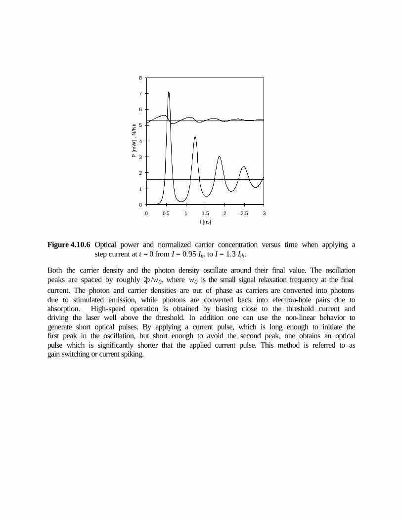
t [ns]
P [m
W] ,
N/N
tr
0
1
2
3
4
5
6
7
8
0 0.5 1 1.5 2 2.5 3
Figure 4.10.6 Optical power and normalized carrier concentration versus time when applying a step current at t = 0 from I = 0.95 Ith to I = 1.3 Ith.
Both the carrier density and the photon density oscillate around their final value. The oscillation peaks are spaced by roughly 2π/ω0, where ω0 is the small signal relaxation frequency at the final current. The photon and carrier densities are out of phase as carriers are converted into photons due to stimulated emission, while photons are converted back into electron-hole pairs due to absorption. High-speed operation is obtained by biasing close to the threshold current and driving the laser well above the threshold. In addition one can use the non-linear behavior to generate short optical pulses. By applying a current pulse, which is long enough to initiate the first peak in the oscillation, but short enough to avoid the second peak, one obtains an optical pulse which is significantly shorter that the applied current pulse. This method is referred to as gain switching or current spiking.
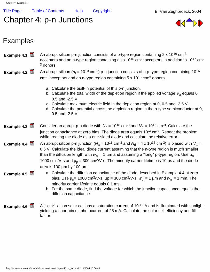
Chapter 4 Examples
Title Page Table of Contents Help Copyright B. Van Zeghbroeck, 2004
Chapter 4: p-n Junctions
Examples
Example 4.1 An abrupt silicon p-n junction consists of a p-type region containing 2 x 1016 cm-3 acceptors and an n-type region containing also 1016 cm-3 acceptors in addition to 1017 cm-3 donors.
Example 4.2 An abrupt silicon (nI = 1010 cm-3) p-n junction consists of a p-type region containing 1016 cm-3 acceptors and an n-type region containing 5 x 1016 cm-3 donors.
a. Calculate the built-in potential of this p-n junction.b. Calculate the total width of the depletion region if the applied voltage Va equals 0,
0.5 and -2.5 V.c. Calculate maximum electric field in the depletion region at 0, 0.5 and -2.5 V.d. Calculate the potential across the depletion region in the n-type semiconductor at 0,
0.5 and -2.5 V.
Example 4.3 Consider an abrupt p-n diode with Na = 1018 cm-3 and Nd = 1016 cm-3. Calculate the junction capacitance at zero bias. The diode area equals 10-4 cm2. Repeat the problem while treating the diode as a one-sided diode and calculate the relative error.
Example 4.4 An abrupt silicon p-n junction (Na = 1016 cm-3 and Nd = 4 x 1016 cm-3) is biased with Va = 0.6 V. Calculate the ideal diode current assuming that the n-type region is much smaller than the diffusion length with wn' = 1 µm and assuming a "long" p-type region. Use µn = 1000 cm2/V-s and µp = 300 cm2/V-s. The minority carrier lifetime is 10 µs and the diode area is 100 µm by 100 µm.
Example 4.5 a. Calculate the diffusion capacitance of the diode described in Example 4.4 at zero bias. Use µn= 1000 cm2/V-s, µp = 300 cm2/V-s, wp' = 1 µm and wn' = 1 mm. The minority carrier lifetime equals 0.1 ms.
b. For the same diode, find the voltage for which the junction capacitance equals the diffusion capacitance.
Example 4.6 A 1 cm2 silicon solar cell has a saturation current of 10-12 A and is illuminated with sunlight yielding a short-circuit photocurrent of 25 mA. Calculate the solar cell efficiency and fill factor.
http://ece-www.colorado.edu/~bart/book/book/chapter4/ch4_ex.htm11/10/2004 16:56:48

Example 4.1 An abrupt silicon p-n junction consists of a p-type regioncontaining 2 x 1016 cm-3 acceptors and an n-type regioncontaining also 1016 cm-3 acceptors in addition to 1017 cm-3
donors.a. Calculate the thermal equilibrium density of electrons
and holes in the p-type region as well as both densities inthe n-type region.
b. Calculate the built-in potential of the p-n junction.c. Calculate the built-in potential of the p-n junction at 400
K.Solution a. The thermal equilibrium densities are:
In the p-type region:p = Na = 2 x 1016 cm-3
n = ni2/p = 1020/2 x 1016 = 5 x 103 cm-3
In the n-type regionn = Nd - Na = 9 x 1016 cm-3
p = ni2/n = 1020/1 x 1016 = 1.11 x 103 cm-3
b. The built-in potential is obtained from
2lni
npti n
npV=φ =
20
1616
10
109102ln0259.0
×××= 0.79 V
c. Similarly, the built-in potential at 400 K equals
2ln
i
npti n
npV=φ =
212
1616
)1052.4(
109102ln0345.0
××××
= 0.63 V
where the intrinsic carrier density at 400 K was obtainedfrom Example 2.4 b.

Example 4.2 An abrupt silicon (ni = 1010 cm-3) p-n junction consists of a p-type region containing 1016 cm-3 acceptors and an n-type regioncontaining 5 x 1016 cm-3 donors.
a. Calculate the built-in potential of this p-n junction.b. Calculate the total width of the depletion region if the
applied voltage Va equals 0, 0.5 and -2.5 V.c. Calculate maximum electric field in the depletion region
at 0, 0.5 and -2.5 V.d. Calculate the potential across the depletion region in the
n-type semiconductor at 0, 0.5 and -2.5 V.The built-in potential is calculated from:
2ln
i
pnti n
npV=φ =
20
1616
10
10510ln0259.0
××= 0.76 V
The depletion layer width is obtained from:
))(11
(2
aida
s VNNq
w −+= φε
the electric field from
w
Vx ai )(2
)0(−
−==φE
and the potential across the n-type region equals
s
nd
n
xNq
εφ
2
2
=
where
da
an NN
Nwx
+=
one can also show that
da
aain NN
NV
+−
=)(φ
φ
This yields the following numeric values:
Va = 0 V Va = 0.5 V Va = -2.5 Vw 0.315 µm 0.143 µm 0.703 µmE 40 kV/cm 18 kV/cm 89 kV/cmφn 0.105 V 0.0216 V 0.522 V

Example 4.3 An abrupt silicon p-n junction (Na = 1016 cm-3 and Nd = 4 x 10¹⁶
cm-3) is biased with Va = 0.6 V. Calculate the ideal diode currentassuming that the n-type region is much smaller than thediffusion length with wn
' = 1 µm and assuming a "long" p-typeregion. Use µn = 1000 cm2/V-s and µp = 300 cm2/V-s. Theminority carrier lifetime is 10 µs and the diode area is 100 µmby 100 µm.The current is calculated from:
)1]([ /
'
00 −+= ta VV
n
np
n
pn ew
pD
L
nDAqI
withDn = µn Vt = 1000 x 0.0258 = 25.8 cm2/V-sDP = µP Vt = 300 x 0.0258 = 7.75 cm2/V-s
np0 = ni2/Na = 1020/1016 = 104 cm-3
pn0 = ni2/Nd = 1020/4 x 1016 = 2.5 x 103 cm-3
=×== −5108.25nnn DL τ 161 µm
yielding I = 40.7 µΑNote that the hole diffusion current occurs in the "short" n-typeregion and therefore depends on the quasi-neutral width in thatregion. The electron diffusion current occurs in the "long" p-typeregion and therefore depends on the electron diffusion length inthat region.

Example 4.4 Consider an abrupt p-n diode with Na = 1018 cm-3 and Nd = 1016
cm-3. Calculate the junction capacitance at zero bias. The diodearea equals 10-4 cm2. Repeat the problem while treating thediode as a one-sided diode and calculate the relative error.
Solution The built in potential of the diode equals:
2ln
i
adti
n
NNV=φ = 0.83 V
The depletion layer width at zero bias equals:
d
is
qNw
)0(2 −=
φε= 0.33 µm
And the junction capacitance at zero bias equals:
00
=
=aV
sj w
Cε
= 3.17 pF
Repeating the analysis while treating the diode as a one-sideddiode, one only has to consider the region with the lower dopingdensity so that
w = )(2
aid
sn V
qNx −= φ
ε= 0.31 µm
And the junction capacitance at zero bias equals
00
=
=aV
sj w
Cε
= 3.18 pF
The relative error equals 0.5 %, which justifies the use of theone-sided approximation.

Example 4.5 a. Calculate the diffusion capacitance of the diode described inExample 4.4 at zero bias. Use µn = 1000 cm2/V-s, µp = 300cm2/V-s, wp' = 1 µm and wn' = 1 mm. The minority carrierlifetime equals 0.1 ms.
b. For the same diode, find the voltage for which the junctioncapacitance equals the diffusion capacitance.
Solution a. The diffusion capacitance at zero volts equals
t
nrns
t
ppsd V
tI
V
IC ,,,
0, +=τ
= 1.73 x 10⁻¹⁹ F
using
p
pnps L
DpAqI 0
, =
and
'
0,
p
npns w
DnAqI =
Where the "short" diode expression was used for thecapacitance associated with the excess charge due toelectrons in the p-type region. The "long" diode expressionwas used for the capacitance associated with the excesscharge due to holes in the n-type region.The diffusion constants and diffusion lengths equal
Dn = µn x Vt = 25.8 cm2/sDp = µp x Vt = 7.75 cm2/s
ppp DL τ=
And the electron transit time in the p-type region equals
n
pnr D
wt
2
2'
, = =193 ps
b. The voltage at which the junction capacitance equals thediffusion capacitance is obtained by solving
ta VVd
i
a
j CV
C /0,
0 e
1
=
−φ
yielding Va = 0.442 V
:

Example 4.6 A 1 cm2 silicon solar cell has a saturation current of 10-12 A andis illuminated with sunlight yielding a short-circuit photocurrentof 25 mA. Calculate the solar cell efficiency and fill factor.
Solution The maximum power is generated for:
tmtm VVs
t
mph
VVs
a
IV
VII
dV
dP // e)1e(0 +−−==
where the voltage, Vm, is the voltage corresponding to themaximum power point. This voltage is obtained by solving thefollowing transcendental equation:
tm
sphtm VV
IIVV
/1
/1ln
+
+=
Using iteration and a starting value of 0.5 V one obtains thefollowing successive values for Vm:
Vm = 0.5, 0.542, 0.540 Vand the efficiency equals:
% 131.0
024.054.0=
×==
in
mm
P
IVη
The current, Im, corresponding to the voltage, Vm, was calculatedusing equation (4.6.1) and the power of the sun was assumed100 mW/cm2. The fill factor equals:
% 83025.062.0
024.054.0factor fill =
××
==scoc
mm
IV
IV
where the open circuit voltage is calculated using equation(4.6.1) and I = 0. The short circuit current equals thephotocurrent.

http://ece-www.colorado.edu/~bart/book/book/chapter4/ch4_p.htm
Title Page Table of Contents Help Copyright B. Van Zeghbroeck, 2004
Chapter 4: p-n Junctions
Problems
1. A silicon p-n junction (Na = 1016 cm-3 and Nd = 4 x 1016 cm-3) is biased with Va = -3 V. Calculate the built-in potential, the depletion layer width and the maximum electric field of the junction.
2. An abrupt silicon p-n junction consists of a p-type region containing 1016 cm-3 acceptors and an n-type region containing also 1016 cm-3 acceptors in addition to 1017 cm-3 donors.
a. Calculate the thermal equilibrium density of electrons and holes in the p-type region as well as both densities in the n-type region.
b. Calculate the built-in potential of the p-n junction. c. Calculate the built-in potential of the p-n junction at 100°C.
3. For a p-n junction with a built-in potential of 0.62 V a. What is the potential across the depletion region at an applied voltage, Va, of 0, 0.5 and -2 Volt? b. If the depletion layer is 1 micrometer at Va = 0 Volt, find the maximum electric field in the depletion
region. c. Assuming that the net doping density |Nd - Na| is the same in the n-type and p-type region of the
diode, carefully sketch the electric field and the potential as a function of position throughout the depletion region. Add numeric values wherever possible.
4.
5. An abrupt silicon (ni = 1010 cm-3) p-n junction consists of a p-type region containing 1016 cm-3 acceptors and an n-type region containing 5 x 1016 cm-3 donors.
a. Calculate the built-in potential of this p-n junction. b. Calculate the total width of the depletion region if the applied voltage, Va equals 0, 0.5 and -2.5 V. c. Calculate maximum electric field in the depletion region at 0, 0.5 and -2.5 V. d. Calculate the potential across the depletion region in the n-type semiconductor at 0, 0.5 and -2.5
V.
6. Consider an abrupt p-n diode in thermal equilibrium with as many donors in the n-type region as acceptors in the p-type region and a maximum electric field of -13 kV/cm and a total depletion layer width of 1 µm. (assume εs/ ε0 = 12)
a. What is the applied voltage, Va? b. What is the built-in potential of the diode? c. What is the donor density in the n-type region and the acceptor density in the p-type region? d. What is the intrinsic carrier density of the semiconductor if the temperature is 300 K ?
7. A silicon (nI = 1010 cm-3) p-n diode with Na = 1018 cm-3 has a capacitance of 10-8 F/cm2 at an applied voltage of 0.5 V. Find the donor density.
http://ece-www.colorado.edu/~bart/book/book/chapter4/ch4_p.htm (1 of 3)11/10/2004 16:58:09

http://ece-www.colorado.edu/~bart/book/book/chapter4/ch4_p.htm
8. A silicon (ni = 1010 cm-3) p-n diode has a maximum electric field of -106 V/cm and a depletion layer width of 1 µm. The acceptor density in the p-type region is four times larger than the donor density in the n-type region. Calculate both doping densities.
9. Consider a symmetric silicon p-n diode (Na = Nd)a. Calculate the built-in potential if Na = 1013, 1015 and 1017 cm-3. Also, calculate the doping
densities corresponding to a built-in potential of 0.7 V.b. For the same as in part a), calculate the total depletion layer widths, the capacitance per unit area
and the maximum electric field in thermal equilibrium.c. For the same as in part a), calculate the total depletion layer widths, the capacitance per unit area
and the maximum electric field in thermal equilibrium.d. Repeat part a) and b) with Na = 3 Nd.
10. A one-sided silicon diode has a breakdown voltage of 1000 V for which the maximum electric field at breakdown is 100 kV/cm. What is the maximum possible doping density in the low doped region, the built-in potential, the depletion layer width and the capacitance per unit area? Assume that bulk potential of the highly doped region is Eg/2 (= 0.56 V).
11. A silicon p-n junction (Na = 1016 cm-3 and Nd = 4 x 1016 cm-3) is biased with Va = 0.6 V. Calculate the ideal diode current assuming that the n-type region is much smaller than the diffusion length with wn' = 1 µm and assuming a "long" p-type region. Use µn = 1000 cm2/V-s and µp = 300 cm2/V-s. The minority carrier lifetime is 10 µs and the diode area is 100 µm by 100 µm.
12. Derive equation 4.4.24.
13. Calculate the relative error when using the "short diode" approximation if Ln = 2 wp' and Lp = 2 wn'.
14. A silicon p-n junction (Na = 1015 cm-3, wp = 1 µm and Nd = 4 x 1016 cm-3, wn = 1 µm) is biased with Va = 0.5 V. Use µn = 1000 cm2/V-s and µp = 300 cm2/V-s. The minority carrier lifetime is 10 µs and the diode area is 100 µm by 100 µm.
a. Calculate the built-in potential of the diode. b. Calculate the depletion layer widths, xn and xp, and the widths of the quasi-neutral regions. c. Compare the width of the quasi-neutral regions with the minority-carrier diffusion-lengths and
decide whether to use the "long" or "short" diode approximation. Calculate the current through the diode.
d. Compare the result of part c) with the current obtained by using the general solution (equation 4.4.24)
e. Using the approximation chosen in part c) calculate the ratio of the electron current to the hole current traversing the depletion region.
15. An abrupt silicon p-n diode consists of a p-type region containing 1018 cm-3 acceptors and an n-type region containing 1015 cm-3 donors.
a. Calculate the breakdown field in the n-type region. b. Using the breakdown field from part a), calculate the breakdown voltage of the diode. c. What is the depletion layer width at breakdown? d. Discuss edge effects and specify the minimum junction depth needed to avoid these effects.
http://ece-www.colorado.edu/~bart/book/book/chapter4/ch4_p.htm (2 of 3)11/10/2004 16:58:09

http://ece-www.colorado.edu/~bart/book/book/chapter4/ch4_p.htm
16. A 1 cm2 solar cell consists of a p-type region containing 1018 cm-3 acceptors and an n-type region containing 1015 cm-3 donors. wp' = 0.1 µm and wn >> Lp. Use µn = 1000 cm2/V-s and µp = 300 cm2/V-s. . The minority carrier lifetime is 10 µs . The diode is illuminated with sun light, yielding a photocurrent density of 30 mA/cm2.
a. Calculate the open circuit voltage and short-circuit current of the solar cell. b. Calculate the maximum power generated by the call and the corresponding voltage and current. c. Calculate the fill factor of the solar cell. d. Calculate the fill factor for the same cell when it is illuminated by a concentrator so that the
photocurrent density equals 300 A/cm2.
17. same as 3
http://ece-www.colorado.edu/~bart/book/book/chapter4/ch4_p.htm (3 of 3)11/10/2004 16:58:09

http://ece-www.colorado.edu/~bart/book/book/chapter4/ch4_r.htm
Title Page Table of Contents Help Copyright B. Van Zeghbroeck, 2004
Chapter 4: p-n Junctions
Review Questions
1. What is a flatband diagram?
2. Discuss the motion of electrons and holes in a p-n junction in thermal equilibrium.
3. Define the built-in potential. Also provide an equation and state the implicit assumption(s).
4. How does the energy band diagram of a p-n junction change under forward and reverse bias?
5. What is the full depletion approximation? Why do we need the full depletion approximation?
6. Derive equation (4.3.17) from (4.3.13), (4.3.14) and (4.3.16).
7. Explain why the capacitance of a p-n junction (4.3.22) equals that of a parallel plate capacitor. How does the capacitance differ from a parallel plate capacitor?
8. How do you extract the doping profile shown in Fig. 4.3.4 from the capacitance shown in Fig. 4.3.3?
9. What mechanism(s) cause(s) current in a p-n junction?
10. How does one calculate the current in a p-n junction?
11. How does one solve the diffusion equation in the quasi-neutral regions?
12. What is the difference between the "long" and "short" diode analysis?
13. When can the recombination/generation current in the depletion region be ignored?
14. Which saturation current is voltage dependent, that for the "long" diode or the one for the "short" diode?
15. Why does one need to include edge effects when calculating the breakdown voltage of a diode?
16. Name two breakdown mechanisms and discuss the temperature dependence of the resulting breakdown voltage.
17. Describe the avalanche breakdown mechanism.
18. Describe tunneling.
19. Illustrate the generation of a photocurrent in a p-n diode by drawing an energy band diagram. Indicate
http://ece-www.colorado.edu/~bart/book/book/chapter4/ch4_r.htm (1 of 2)11/10/2004 16:58:25

http://ece-www.colorado.edu/~bart/book/book/chapter4/ch4_r.htm
the photo-generated carriers and their direction of motion.
20. Why is the photocurrent negative compared to the forward bias current through the same diode?
21. What limits the quantum efficiency of a photodiode?
22. What is the difference between a solar cell and a photodiode?
23. Why would solar cells be more efficient if the sun where a laser rather than a black body radiator?
24. What limits the power conversion efficiency of a solar cell?
25. Using equation 4.6.1 show that the open-circuit voltage increases as the photocurrent increases. Use this result to prove that the power conversion efficiency of a solar increases when using a concentrator which increases the incident power density.
26. Why is silicon not used to fabricated LEDs or laser diodes?
27. Why are planar LEDs so inefficient? How can the efficiency of an LED be improved beyond that of a planar LED?
28. How does the light emitted by an LED differ from that emitted by a laser diode?
29. What is stimulated emission?
30. Why does a laser diode need a waveguide?
31. Explain the lasing condition in words.
32. Describe the power versus current characteristic of a laser diode.
http://ece-www.colorado.edu/~bart/book/book/chapter4/ch4_r.htm (2 of 2)11/10/2004 16:58:25

Chapter 4 Bibliography
Title Page Table of Contents Help Copyright B. Van Zeghbroeck, 2004
Chapter 4: p-n Junctions
Bibliography
http://ece-www.colorado.edu/~bart/book/book/chapter4/ch4_b.htm11/10/2004 16:58:32

Chapter 4 Equations
Title Page Table of Contents Help Copyright B. Van Zeghbroeck, 2004
Chapter 4: p-n Junctions
Equations
(4.2.1)
(4.2.2)
(4.3.1)
(4.3.2)
(4.3.3)
(4.3.4)
(4.3.5)
(4.3.6)
http://ece-www.colorado.edu/~bart/book/book/chapter4/ch4_eq.htm (1 of 10)11/10/2004 16:58:39

Chapter 4 Equations
(4.3.7)
(4.3.8)
(4.3.9)
(4.3.10)
(4.3.11)
(4.3.12)
(4.3.13)
(4.3.14)
(4.3.15)
http://ece-www.colorado.edu/~bart/book/book/chapter4/ch4_eq.htm (2 of 10)11/10/2004 16:58:39

Chapter 4 Equations
(4.3.16)
(4.3.17)
(4.3.18)
(4.3.19)
(4.3.20)
(4.3.21)
(4.3.22)
(4.3.23)
(4.3.24)
(4.3.25)
http://ece-www.colorado.edu/~bart/book/book/chapter4/ch4_eq.htm (3 of 10)11/10/2004 16:58:39

Chapter 4 Equations
(4.3.23)
(4.4.1)
(4.4.2)
(4.4.3)
(4.4.4)
(4.4.5)
(4.4.6)
(4.4.7)
(4.4.8)
(4.4.9)
http://ece-www.colorado.edu/~bart/book/book/chapter4/ch4_eq.htm (4 of 10)11/10/2004 16:58:39
Chapter 4 Equations
(4.4.10)
(4.4.11)
(4.4.12)
(4.4.13)
(4.4.14)
(4.4.15)
(4.4.16)
(4.4.17)
(4.4.18)
http://ece-www.colorado.edu/~bart/book/book/chapter4/ch4_eq.htm (5 of 10)11/10/2004 16:58:39

Chapter 4 Equations
(4.4.19)
(4.4.20)
(4.4.21)
(4.4.22)
(4.4.23)
(4.4.24)
(4.4.25)
(4.4.26)
(4.4.27)
(4.4.28)
http://ece-www.colorado.edu/~bart/book/book/chapter4/ch4_eq.htm (6 of 10)11/10/2004 16:58:39

Chapter 4 Equations
(4.4.29)
(4.4.30)
(4.4.31)
(4.4.32)
(4.4.33)
(4.4.34)
(4.4.35)
(4.4.36)
(4.4.37)
(4.4.38)
http://ece-www.colorado.edu/~bart/book/book/chapter4/ch4_eq.htm (7 of 10)11/10/2004 16:58:39

Chapter 4 Equations
(4.4.39)
(4.4.40)
(4.4.41)
(4.4.42)
(4.4.43)
(4.4.44)
(4.4.45)
(4.4.46)
(4.4.47)
(4.4.48)
http://ece-www.colorado.edu/~bart/book/book/chapter4/ch4_eq.htm (8 of 10)11/10/2004 16:58:39
Chapter 4 Equations
(4.4.49)
(4.5.1)
(4.5.2)
(4.5.3)
(4.5.4)
(4.5.5)
(4.5.6)
(4.5.7)
(4.5.8)
(4.6.1)
http://ece-www.colorado.edu/~bart/book/book/chapter4/ch4_eq.htm (9 of 10)11/10/2004 16:58:39
Chapter 4 Equations
(4.6.2)
(4.6.3)
(4.6.4)
(4.6.5)
(4.6.6)
(4.6.7)
(4.6.8)
http://ece-www.colorado.edu/~bart/book/book/chapter4/ch4_eq.htm (10 of 10)11/10/2004 16:58:39

Bipolar Junction Transistors
Title Page Table of Contents Help Copyright B. Van Zeghbroeck, 2004
Chapter 5: Bipolar Junction Transistors
5.1. Introduction
The bipolar junction transistor was the first solid-state amplifier element and started the solid-state electronics revolution. Bardeen, Brattain and Shockley at the Bell Laboratories invented it in 1948 as part of a post-war effort to replace vacuum tubes with solid-state devices. Solid-state rectifiers were already in use at the time and were preferred over vacuum diodes because of their smaller size, lower weight and higher reliability. A solid-state replacement for a vacuum triode was expected to yield similar advantages. The work at Bell Laboratories was highly successful and culminated in Bardeen, Brattain and Shockley receiving the Nobel Prize in 1956.Their work led them first to the point-contact transistor and then to the bipolar junction transistor. They used germanium as the semiconductor of choice because it was possible to obtain high purity material. The extraordinarily large diffusion length of minority carriers in germanium provided functional structures despite the large dimensions of the early devices.Since then, the technology has progressed rapidly. The development of a planar process yielded the first circuits on a chip and for a decade, bipolar transistor operational amplifiers, like the 741, and digital TTL circuits were the workhorses of any circuit designer.The spectacular rise of the MOSFET market share during the last decade has completely removed the bipolar transistor from center stage. Almost all logic circuits, microprocessor and memory chips contain exclusively MOSFETs.Nevertheless, bipolar transistors remain important devices for ultra-high-speed discrete logic circuits such as emitter coupled logic (ECL), power-switching applications and in microwave power amplifiers.In this chapter we first present the structure of the bipolar transistor and show how a three-layer structure with alternating n-type and p-type regions can provide current and voltage amplification. We then present the ideal transistor model and derive an expression for the current gain in the forward active mode of operation. Next, we discuss the non-ideal effects, the modulation of the base width and recombination in the depletion region of the base-emitter junction.
http://ece-www.colorado.edu/~bart/book/book/chapter5/ch5_1.htm11/10/2004 16:58:58

Bipolar Junction Transistors
Title Page Table of Contents Help Copyright B. Van Zeghbroeck, 2004
Chapter 5: Bipolar Junction Transistors
5.2. Structure and principle of operation
A bipolar junction transistor consists of two back-to-back p-n junctions, who share a thin common region with width, wB. Contacts are made to all three regions, the two outer regions called the emitter and collector and the middle region called the base. The structure of an NPN bipolar transistor is shown in Figure 5.2.1 (a). The device is called "bipolar" since its operation involves both types of mobile carriers, electrons and holes.
Figure 5.2.1.: (a) Structure and sign convention of a NPN bipolar junction transistor. (b) Electron and hole flow under forward active bias, VBE > 0 and VBC = 0.
http://ece-www.colorado.edu/~bart/book/book/chapter5/ch5_2.htm (1 of 5)11/10/2004 17:00:25

Bipolar Junction Transistors
Since the device consists of two back-to-back diodes, there are depletion regions between the quasi-neutral regions. The width of the quasi neutral regions in the emitter, base and collector are indicated with the symbols wE', wB' and wC' and are calculated from
(5.2.1)
(5.2.2)
(5.2.3)
where the depletion region widths are given by:
(5.2.4)
(5.2.5)
(5.2.6)
(5.2.7)
with
(5.2.8)
(5.2.9)
The sign convention of the currents and voltage is indicated on Figure 5.2.1(a). The base and collector current are positive if a positive current goes into the base or collector contact. The emitter current is positive for a current coming out of the emitter contact. This also implies the emitter current, IE, equals the sum of the base current, IB, and the collector current, IC:
(5.2.10)
The base-emitter voltage and the base-collector voltage are positive if a positive voltage is applied to the base contact relative to the emitter and collector respectively.
http://ece-www.colorado.edu/~bart/book/book/chapter5/ch5_2.htm (2 of 5)11/10/2004 17:00:25
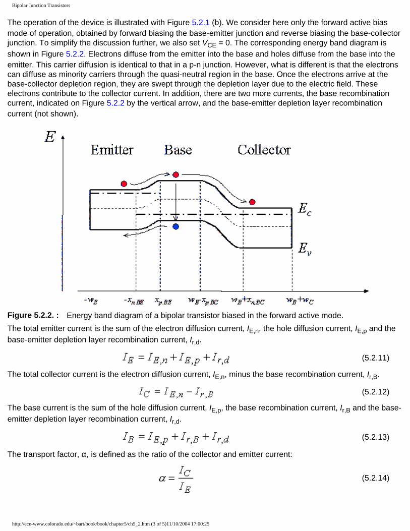
Bipolar Junction Transistors
The operation of the device is illustrated with Figure 5.2.1 (b). We consider here only the forward active bias mode of operation, obtained by forward biasing the base-emitter junction and reverse biasing the base-collector junction. To simplify the discussion further, we also set VCE = 0. The corresponding energy band diagram is shown in Figure 5.2.2. Electrons diffuse from the emitter into the base and holes diffuse from the base into the emitter. This carrier diffusion is identical to that in a p-n junction. However, what is different is that the electrons can diffuse as minority carriers through the quasi-neutral region in the base. Once the electrons arrive at the base-collector depletion region, they are swept through the depletion layer due to the electric field. These electrons contribute to the collector current. In addition, there are two more currents, the base recombination current, indicated on Figure 5.2.2 by the vertical arrow, and the base-emitter depletion layer recombination current (not shown).
Figure 5.2.2. : Energy band diagram of a bipolar transistor biased in the forward active mode.The total emitter current is the sum of the electron diffusion current, IE,n, the hole diffusion current, IE,p and the base-emitter depletion layer recombination current, Ir,d.
(5.2.11)
The total collector current is the electron diffusion current, IE,n, minus the base recombination current, Ir,B.
(5.2.12)
The base current is the sum of the hole diffusion current, IE,p, the base recombination current, Ir,B and the base-emitter depletion layer recombination current, Ir,d.
(5.2.13)
The transport factor, α, is defined as the ratio of the collector and emitter current:
(5.2.14)
http://ece-www.colorado.edu/~bart/book/book/chapter5/ch5_2.htm (3 of 5)11/10/2004 17:00:25

Bipolar Junction Transistors
Using Kirchoff's current law and the sign convention shown in Figure 5.2.1(a), we find that the base current equals the difference between the emitter and collector current. The current gain, β, is defined as the ratio of the collector and base current and equals:
(5.2.15)
This explains how a bipolar junction transistor can provide current amplification. If the collector current is almost equal to the emitter current, the transport factor, α, approaches one. The current gain, β, can therefore become much larger than one.
To facilitate further analysis, we now rewrite the transport factor, α, as the product of the emitter efficiency, γE, the base transport factor, αT, and the depletion layer recombination factor, δr.
(5.2.16)
The emitter efficiency, γE, is defined as the ratio of the electron current in the emitter, IE,n, to the sum of the electron and hole current diffusing across the base-emitter junction, IE,n + IE,p.
(5.2.17)
The base transport factor, αT, equals the ratio of the current due to electrons injected in the collector, to the current due to electrons injected in the base.
(5.2.18)
Recombination in the depletion-region of the base-emitter junction further reduces the current gain, as it increases the emitter current without increasing the collector current. The depletion layer recombination factor, δr, equals the ratio of the current due to electron and hole diffusion across the base-emitter junction to the total emitter current:
(5.2.19)
Example 5.1 A bipolar transistor with an emitter current of 1 mA has an emitter efficiency of 0.99, a base transport factor of 0.995 and a depletion layer recombination factor of 0.998. Calculate the base current, the collector current, the transport factor and the current gain of the transistor.
http://ece-www.colorado.edu/~bart/book/book/chapter5/ch5_2.htm (4 of 5)11/10/2004 17:00:25

Bipolar Junction Transistors
Solution The transport factor and current gain are:
and
The collector current then equals
And the base current is obtained from:
http://ece-www.colorado.edu/~bart/book/book/chapter5/ch5_2.htm (5 of 5)11/10/2004 17:00:25

Bipolar Junction Transistors
Title Page Table of Contents Help Copyright B. Van Zeghbroeck, 2004
Chapter 5: Bipolar Junction Transistors
5.3. Ideal transistor model5.3.1. Forward active mode of operation5.3.2. General bias modes of a bipolar transistor5.3.3. The Ebers-Moll model5.3.4. Saturation.
The ideal transistor model is based on the ideal p-n diode model and provides a first-order calculation of the dc parameters of a bipolar junction transistor. To further simplify this model, we will assume that all quasi-neutral regions in the device are much smaller than the minority-carrier diffusion lengths in these regions, so that the "short" diode expressions apply. The use of the ideal p-n diode model implies that no recombination within the depletion regions is taken into account. Such recombination current will be discussed in section 5.4.3.
The discussion of the ideal transistor starts with a discussion of the forward active mode of operation, followed by a general description of the four different bias modes, the corresponding Ebers-Moll model and a calculation of the collector-emitter voltage when the device is biased in saturation.
5.3.1.. Forward active mode of operation
The forward active mode is obtained by forward-biasing the base-emitter junction. In addition we eliminate the base-collector junction current by setting VBC = 0. The minority-carrier distribution in the quasi-neutral regions of the bipolar transistor, as shown in Figure 5.3.1, is used to analyze this situation in more detail.
http://ece-www.colorado.edu/~bart/book/book/chapter5/ch5_3.htm (1 of 8)11/10/2004 17:00:38

Bipolar Junction Transistors
Figure 5.3.1. : Minority-carrier distribution in the quasi-neutral regions of a bipolar transistor (a) Forward active bias mode. (b) Saturation mode.
The values of the minority carrier densities at the edges of the depletion regions are indicated on the Figure 5.3.1. The carrier densities vary linearly between the boundary values as expected when using the assumption that no significant recombination takes place in the quasi-neutral regions. The minority carrier densities on both sides of the base-collector depletion region equal the thermal equilibrium values since VBC was set to zero. While this boundary condition is mathematically equivalent to that of an ideal contact, there is an important difference. The minority carriers arriving at x = wB - xp,C do not recombine. Instead, they drift through the base-collector depletion region and end up as majority carriers in the collector region.The emitter current due to electrons and holes are obtained using the "short" diode expressions derived in section 4.4.2.5, yielding:
(5.3.1)
and
(5.3.2)
It is convenient to rewrite the emitter current due to electrons, IE,n, as a function of the total excess minority charge in the base, ∆Qn,B. This charge is proportional to the triangular area in the quasi-neutral base as shown in Figure 5.3.1 a) and is calculated from:
http://ece-www.colorado.edu/~bart/book/book/chapter5/ch5_3.htm (2 of 8)11/10/2004 17:00:38

Bipolar Junction Transistors
(5.3.3)
which for a "short" diode becomes:
(5.3.4)
And the emitter current due to electrons, IE,n, simplifies to:
(5.3.5)
where tr is the average time the minority carriers spend in the base layer, i.e. the transit time. The emitter current therefore equals the excess minority carrier charge present in the base region, divided by the time this charge spends in the base. This and other similar relations will be used to construct the charge control model of the bipolar junction transistor in section 5.5.2.
A combination of equations (5.3.1), (5.3.4) and (5.3.5) yields the transit time as a function of the quasi-neutral layer width, wB', and the electron diffusion constant in the base, Dn,B.
(5.3.6)
We now turn our attention to the recombination current in the quasi-neutral base and obtain it from the continuity equation:
(5.3.7)
In steady state and applied to the quasi-neutral region in the base, the continuity equation yields the base recombination current, Ir,B:
(5.3.8)
which in turn can be written as a function of the excess minority carrier charge, ∆Qn,B, using equation (5.3.3).
(5.3.9)
Next, we need to find the emitter efficiency and base transport factor. The emitter efficiency defined by equation (5.2.17), becomes:
http://ece-www.colorado.edu/~bart/book/book/chapter5/ch5_3.htm (3 of 8)11/10/2004 17:00:38
Bipolar Junction Transistors
(5.3.10)
It is typically the emitter efficiency, which limits the current gain in transistors made of silicon or germanium. The long minority-carrier lifetime and the long diffusion lengths in those materials justify the exclusion of recombination in the base or the depletion layer. The resulting current gain, under such conditions, is:
(5.3.11)
From this equation, we conclude that the current gain can be larger than one if the emitter doping is much larger than the base doping. A typical current gain for a silicon bipolar transistor is 50 - 150.The base transport factor, as defined in equation (5.2.18), equals:
(5.3.12)
This expression is only valid if the base transport factor is very close to one, since it was derived using the "short-diode" carrier distribution. This base transport factor can also be expressed in function of the diffusion length in the base:
(5.3.13)
Example 5.2 Consider a pnp bipolar transistor with emitter doping of 1018 cm-3 and base doping of 1017 cm-3. The quasi-neutral region width in the emitter is 1 µm and 0.2 µm in the base. Use µn = 1000 cm2/V-s and µp = 300 cm2/V-s . The minority carrier lifetime in the base is 10 ns.Calculate the emitter efficiency, the base transport factor, and the current gain of the transistor biased in the forward active mode. Assume there is no recombination in the depletion region.
Solution The emitter efficiency is obtained from:
The base transport factor equals:
The current gain then becomes:
http://ece-www.colorado.edu/~bart/book/book/chapter5/ch5_3.htm (4 of 8)11/10/2004 17:00:38

Bipolar Junction Transistors
where the transport factor, α, was calculated as the product of the emitter efficiency and the base transport factor:
5.3.2.. General bias modes of a bipolar transistor
While the forward active mode of operation is the most useful bias mode when using a bipolar junction transistor as an amplifier, one cannot ignore the other bias modes especially when using the device as a digital switch. All possible bias modes are illustrated with Figure 5.3.2. They are the forward active mode of operation, the reverse active mode of operation, the saturation mode and the cut-off mode.
Figure 5.3.2.: Possible bias modes of operation of a bipolar junction transistor.The forward active mode is the one where we forward bias the base-emitter junction, VBE > 0 and reverse bias the base-collector junction, VBC < 0. This mode, as discussed in section 5.3.1, is the one used in bipolar transistor amplifiers. In bipolar transistor logic circuits, one frequently switches the transistor from the "off" state to the low resistance "on" state. This "off" state is the cut-off mode and the "on" state is the saturation mode. In the cut-off mode, both junctions are reversed biased, VBE < 0 and VBC < 0, so that very little current goes through the device. This corresponds to the "off" state of the device. In the saturation mode, both junctions are forward biased, VBE > 0 and VCB > 0. This corresponds to the low resistance "on" state of the transistor.
http://ece-www.colorado.edu/~bart/book/book/chapter5/ch5_3.htm (5 of 8)11/10/2004 17:00:38

Bipolar Junction Transistors
Finally, there is the reverse active mode of operation. In the reverse active mode, we reverse the function of the emitter and the collector. We reverse bias the base-emitter junction and forward bias the base-collector junction, or VBE < 0 and VBC > 0. In this mode, the transistor has an emitter efficiency and base transport factor as described by equations ((5.3.10) and (5.3.12), where we replace the emitter parameters by the collector parameters. Most transistors, however, have poor emitter efficiency under reverse active bias since the collector doping density is typically much less than the base doping density to ensure high base-collector breakdown voltages. In addition, the collector-base area is typically larger than the emitter-base area, so that even fewer electrons make it from the collector into the emitter.Having described the forward active mode of operation, there remains the saturation mode, which needs further discussion. Cut-off requires little further analysis, while the reverse active mode of operation is analogous to the forward active mode with the added complication that the areas of the base-emitter and base-collector junction, AE and AC, differ. The Ebers-Moll model describes all of these bias modes.
5.3.3.. The Ebers-Moll model
The Ebers-Moll model is an ideal model for a bipolar transistor, which can be used, in the forward active mode of operation, in the reverse active mode, in saturation and in cut-off. This model is the predecessor of today's computer simulation models and contains only the "ideal" diode currents.The model contains two diodes and two current sources as shown in Figure 5.3.3. The two diodes represent the base-emitter and base-collector diodes. The current sources quantify the transport of minority carriers through the base region. These are current sources depend on the current through each diode. The parameters IE,s, IC,s, αF and αR are the saturation currents of the base-emitter and base collector diode and the forward and reverse transport factors.
Figure 5.3.3 : Equivalent circuit for the Ebers-Moll model of an NPN bipolar junction transistorUsing the parameters identified in Figure 5.3.3, we can relate the emitter, base and collector current to the forward and reverse currents and transport factors, yielding:
http://ece-www.colorado.edu/~bart/book/book/chapter5/ch5_3.htm (6 of 8)11/10/2004 17:00:38

Bipolar Junction Transistors
(5.3.14)
(5.3.15)
(5.3.16)
The Ebers-Moll parameters are related by the following equation:
(5.3.17)
This relation ship is also referred as the reciprocity relation and can be derived by examining the minority carrier current through the base. For the specific case where the base-emitter and base-collector voltage are the same and the base doping is uniform, there can be no minority carrier diffusion in the base so that:
(5.3.18)
from which the reciprocity relation is obtained.The forward- and reverse-bias transport factors are obtained by measuring the current gain in the forward active and reverse active mode of operation. The saturation currents IE,s and IC,s are obtained by measuring the base-emitter (base-collector) diode saturation current while shorting the base-collector (base-emitter) diode.
5.3.4.. Saturation.
In the low resistance "on" state of a bipolar transistor, one finds that the voltage between the collector and emitter is less than the forward bias voltage of the base-emitter junction. Typically the "on" state voltage of a silicon BJT is 100 mV and the forward bias voltage is 700 mV. Therefore, the base-collector junction is forward biased. Using the Ebers-Moll model, we can calculate the "on" voltage from:
(5.3.19)
and using equations (5.3.15), (5.3.16) and the reciprocity relation (5.3.17), one obtains:
(5.3.20)
http://ece-www.colorado.edu/~bart/book/book/chapter5/ch5_3.htm (7 of 8)11/10/2004 17:00:38

Bipolar Junction Transistors
Saturation also implies that a large amount of minority carrier charge is accumulated in the base region. As a transistor is switched from saturation to cut-off, this charge initially remains in the base and a collector current will remain until this charge is removed by recombination. This causes an additional delay before the transistor is turned off. Since the carrier lifetime can be significantly longer than the base transit time, the turn-off delay causes a large and undesirable asymmetry between turn-on and turn-off time. Saturation is therefore avoided in high-speed bipolar logic circuits. Two techniques are used to reduce the turn-off delay: 1) adding a Schottky diode in parallel to the base-collector junction and 2) using an emitter-coupled circuit configuration. Both approaches avoid biasing the transistor in the saturation mode. The Schottky diode clamps the base-collector voltage at a value, which is slightly lower than the turn-on voltage of the base-collector diode. An emitter-coupled circuit is biased with a current source, which can be designed so that the collector voltage cannot be less than the base voltage.Example 5.3 Calculate the saturation voltage of a bipolar transistor biased with a base current of 1 mA and
a collector current of 10 mA. Use αR = 0.993 and αF = 0.2.
Solution The saturation voltage equals:
http://ece-www.colorado.edu/~bart/book/book/chapter5/ch5_3.htm (8 of 8)11/10/2004 17:00:38

Bipolar Junction Transistors
Title Page Table of Contents Help Copyright B. Van Zeghbroeck, 2004
Chapter 5: Bipolar Junction Transistors
5.4. Non-ideal effects5.4.1. Base-width modulation5.4.2. Recombination in the depletion region5.4.3. High injection effects5.4.4. Base spreading resistance and emitter current crowding5.4.5. Temperature dependent effects in bipolar transistors5.4.6. Breakdown mechanisms in BJTs
A variety of effects occur in bipolar transistors, which are not included in the ideal transistor model. These include the base-width modulation effects and the current due to recombination in the depletion layers. Both are described next.
5.4.1.. Base-width modulation
As the voltages applied to the base-emitter and base-collector junctions are changed, the depletion layer widths and the quasi-neutral regions vary as well. This causes the collector current to vary with the collector-emitter voltage as illustrated in Figure 5.4.1.
Figure 5.4.1. : Variation of the minority-carrier distribution in the base quasi-neutral region due to a variation of the base-collector voltage.
http://ece-www.colorado.edu/~bart/book/book/chapter5/ch5_4.htm (1 of 7)11/10/2004 17:00:54
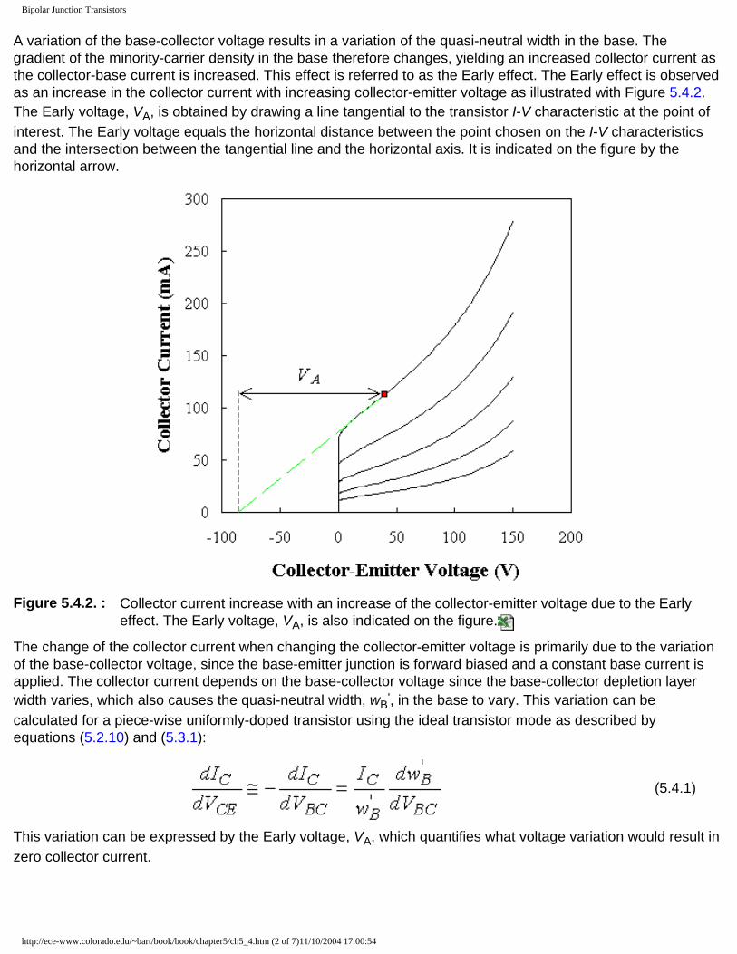
Bipolar Junction Transistors
A variation of the base-collector voltage results in a variation of the quasi-neutral width in the base. The gradient of the minority-carrier density in the base therefore changes, yielding an increased collector current as the collector-base current is increased. This effect is referred to as the Early effect. The Early effect is observed as an increase in the collector current with increasing collector-emitter voltage as illustrated with Figure 5.4.2. The Early voltage, VA, is obtained by drawing a line tangential to the transistor I-V characteristic at the point of interest. The Early voltage equals the horizontal distance between the point chosen on the I-V characteristics and the intersection between the tangential line and the horizontal axis. It is indicated on the figure by the horizontal arrow.
Figure 5.4.2. : Collector current increase with an increase of the collector-emitter voltage due to the Early effect. The Early voltage, VA, is also indicated on the figure.
The change of the collector current when changing the collector-emitter voltage is primarily due to the variation of the base-collector voltage, since the base-emitter junction is forward biased and a constant base current is applied. The collector current depends on the base-collector voltage since the base-collector depletion layer width varies, which also causes the quasi-neutral width, wB', in the base to vary. This variation can be calculated for a piece-wise uniformly-doped transistor using the ideal transistor mode as described by equations (5.2.10) and (5.3.1):
(5.4.1)
This variation can be expressed by the Early voltage, VA, which quantifies what voltage variation would result in zero collector current.
http://ece-www.colorado.edu/~bart/book/book/chapter5/ch5_4.htm (2 of 7)11/10/2004 17:00:54
Bipolar Junction Transistors
(5.4.2)
It can be shown that the Early voltage also equals the majority carrier charge in the base, QB, divided by the base-collector junction capacitance, Cj,BC:
(5.4.3)
In addition to the Early effect, there is a less pronounced effect due to the variation of the base-emitter voltage, which changes the ideality factor of the collector current. However, the effect at the base-emitter junction is much smaller since the base-emitter junction capacitance is larger and the base-emitter voltage variation is very limited since the junction in forward biased. The effect does lead to a variation of the ideality factor, n, given by:
(5.4.4)
Example 5.4 Consider a bipolar transistor with a base doping of 1017 cm-3 and a quasi-neutral base width of 0.2 µm. Calculate the Early voltage and collector current ideality factor given that the base-emitter capacitance and the base-collector capacitance are 0.2 nF and 0.2 pF. The collector area equals 10-4 cm-2.
Solution The Early voltage equals:
The saturation voltage equals:
An extreme case of base-width modulation is punchthrough. As the collector-emitter voltage is increased, the quasi-neutral width of the base decreases, so that eventually it becomes zero. The collector current becomes very large and no longer depends on the voltage applied to the base. This mode of operation is undesirable since most performance characteristics degrade as one approaches punchthrough. The rapid increase of the collector current at the punchthrough voltage can cause the destruction of the transistor due to excessive power dissipation. Punchthrough is therefore one of the possible breakdown modes of a bipolar transistor.
http://ece-www.colorado.edu/~bart/book/book/chapter5/ch5_4.htm (3 of 7)11/10/2004 17:00:54

Bipolar Junction Transistors
5.4.2.. Recombination in the depletion region
So far, we have ignored the recombination in the depletion region. As in a p-n diode, the recombination in the depletion region causes an additional diode current. We can identify this contribution to the current because of the different voltage dependence as described in section 4.4.4. An example is shown in Figure 5.4.3. Shown are the collector and base current of a silicon bipolar transistor, biased in the forward active mode of operation with VBC = -12 V, as a function of the base-emitter voltage. This type of plot is also called a Gummel plot.
Figure 5.4.3 : Gummel plot: Collector current (top curve) and base current (bottom curve) of a silicon bipolar transistor versus the base-emitter voltage.
The current due to recombination in the depletion region can be observed as an additional base current between VBE = 0.2 and 0.4 V. The collector current does not include this additional current, since recombination in the depletion region does not affect the flow of electrons through the base.
5.4.3. High injection effects
High injection effects occur in a bipolar junction transistor, just like in a p-n diode. Since under forward active bias condition only the base-emitter diode is forward biased, one only has to explore the high-injection effects of the base-emitter diode. Again is it the lower doped side of the p-n diode where high injection will occur first so that we examine the high-injection condition in the base region. The onset of high injection is therefore expected if the collector current is equal or larger than:
(5.4.7)
http://ece-www.colorado.edu/~bart/book/book/chapter5/ch5_4.htm (4 of 7)11/10/2004 17:00:54

Bipolar Junction Transistors
High injection effects occur in a bipolar junction transistor, just like in a p-n diode. Since under forward active bias condition only the base-emitter diode is forward biased, one only has to explore the high-injection effects of the base-emitter diode. Again is it the lower doped side of the p-n diode where high injection will occur first so that we examine the high-injection condition in the base region. The onset of high injection is therefore expected if the collector current is equal or larger than:
(5.4.8)High injection effects occur in a bipolar junction transistor, just like in a p-n diode. Since under forward active bias condition only the base-emitter diode is forward biased, one only has to explore the high-injection effects of the base-emitter diode. Again is it the lower doped side of the p-n diode where high injection will occur first so that we examine the high-injection condition in the base region. The onset of high injection is therefore expected if the collector current is equal or larger than:
(5.4.9)High injection effects occur in a bipolar junction transistor, just like in a p-n diode. Since under forward active bias condition only the base-emitter diode is forward biased, one only has to explore the high-injection effects of the base-emitter diode. Again is it the lower doped side of the p-n diode where high injection will occur first so that we examine the high-injection condition in the base region. The onset of high injection is therefore expected if the collector current is equal or larger than:
(5.4.10)High injection effects occur in a bipolar junction transistor, just like in a p-n diode. Since under forward active bias condition only the base-emitter diode is forward biased, one only has to explore the high-injection effects of the base-emitter diode. Again is it the lower doped side of the p-n diode where high injection will occur first so that we examine the high-injection condition in the base region. The onset of high injection is therefore expected if the collector current is equal or larger than:
5.4.4. Base spreading resistance and emitter current crowding
High injection effects occur in a bipolar junction transistor, just like in a p-n diode. Since under forward active bias condition only the base-emitter diode is forward biased, one only has to explore the high-injection effects of the base-emitter diode. Again is it the lower doped side of the p-n diode where high injection will occur first so that we examine the high-injection condition in the base region. The onset of high injection is therefore expected if the collector current is equal or larger than:
(5.4.11)High injection effects occur in a bipolar junction transistor, just like in a p-n diode. Since under forward active bias condition only the base-emitter diode is forward biased, one only has to explore the high-injection effects of the base-emitter diode. Again is it the lower doped side of the p-n diode where high injection will occur first so that we examine the high-injection condition in the base region. The onset of high injection is therefore expected if the collector current is equal or larger than:
(5.4.12)High injection effects occur in a bipolar junction transistor, just like in a p-n diode. Since under forward active bias condition only the base-emitter diode is forward biased, one only has to explore the high-injection effects of the base-emitter diode. Again is it the lower doped side of the p-n diode where high injection will occur first so that we examine the high-injection condition in the base region. The onset of high injection is therefore expected if the collector current is equal or larger than:
(5.4.13)
http://ece-www.colorado.edu/~bart/book/book/chapter5/ch5_4.htm (5 of 7)11/10/2004 17:00:54
Bipolar Junction Transistors
High injection effects occur in a bipolar junction transistor, just like in a p-n diode. Since under forward active bias condition only the base-emitter diode is forward biased, one only has to explore the high-injection effects of the base-emitter diode. Again is it the lower doped side of the p-n diode where high injection will occur first so that we examine the high-injection condition in the base region. The onset of high injection is therefore expected if the collector current is equal or larger than:
(5.4.14)High injection effects occur in a bipolar junction transistor, just like in a p-n diode. Since under forward active bias condition only the base-emitter diode is forward biased, one only has to explore the high-injection effects of the base-emitter diode. Again is it the lower doped side of the p-n diode where high injection will occur first so that we examine the high-injection condition in the base region. The onset of high injection is therefore expected if the collector current is equal or larger than:
5.4.5. Temperature dependent effects in bipolar transistors
High injection effects occur in a bipolar junction transistor, just like in a p-n diode. Since under forward active bias condition only the base-emitter diode is forward biased, one only has to explore the high-injection effects of the base-emitter diode. Again is it the lower doped side of the p-n diode where high injection will occur first so that we examine the high-injection condition in the base region. The onset of high injection is therefore expected if the collector current is equal or larger than: High injection effects occur in a bipolar junction transistor, just like in a p-n diode. Since under forward active bias condition only the base-emitter diode is forward biased, one only has to explore the high-injection effects of the base-emitter diode. Again is it the lower doped side of the p-n diode where high injection will occur first so that we examine the high-injection condition in the base region. The onset of high injection is therefore expected if the collector current is equal or larger than: High injection effects occur in a bipolar junction transistor, just like in a p-n diode. Since under forward active bias condition only the base-emitter diode is forward biased, one only has to explore the high-injection effects of the base-emitter diode. Again is it the lower doped side of the p-n diode where high injection will occur first so that we examine the high-injection condition in the base region. The onset of high injection is therefore expected if the collector current is equal or larger than: High injection effects occur in a bipolar junction transistor, just like in a p-n diode. Since under forward active bias condition only the base-emitter diode is forward biased, one only has to explore the high-injection effects of the base-emitter diode. Again is it the lower doped side of the p-n diode where high injection will occur first so that we examine the high-injection condition in the base region. The onset of high injection is therefore expected if the collector current is equal or larger than:
5.4.6. Recombination in the depletion region
High injection effects occur in a bipolar junction transistor, just like in a p-n diode. Since under forward active bias condition only the base-emitter diode is forward biased, one only has to explore the high-injection effects of the base-emitter diode. Again is it the lower doped side of the p-n diode where high injection will occur first so that we examine the high-injection condition in the base region. The onset of high injection is therefore expected if the collector current is equal or larger than:
http://ece-www.colorado.edu/~bart/book/book/chapter5/ch5_4.htm (6 of 7)11/10/2004 17:00:54
Bipolar Junction Transistors
High injection effects occur in a bipolar junction transistor, just like in a p-n diode. Since under forward active bias condition only the base-emitter diode is forward biased, one only has to explore the high-injection effects of the base-emitter diode. Again is it the lower doped side of the p-n diode where high injection will occur first so that we examine the high-injection condition in the base region. The onset of high injection is therefore expected if the collector current is equal or larger than: High injection effects occur in a bipolar junction transistor, just like in a p-n diode. Since under forward active bias condition only the base-emitter diode is forward biased, one only has to explore the high-injection effects of the base-emitter diode. Again is it the lower doped side of the p-n diode where high injection will occur first so that we examine the high-injection condition in the base region. The onset of high injection is therefore expected if the collector current is equal or larger than: High injection effects occur in a bipolar junction transistor, just like in a p-n diode. Since under forward active bias condition only the base-emitter diode is forward biased, one only has to explore the high-injection effects of the base-emitter diode. Again is it the lower doped side of the p-n diode where high injection will occur first so that we examine the high-injection condition in the base region. The onset of high injection is therefore expected if the collector current is equal or larger than:
(5.4.15)High injection effects occur in a bipolar junction transistor, just like in a p-n diode. Since under forward active bias condition only the base-emitter diode is forward biased, one only has to explore the high-injection effects of the base-emitter diode. Again is it the lower doped side of the p-n diode where high injection will occur first so that we examine the high-injection condition in the base region. The onset of high injection is therefore expected if the collector current is equal or larger than:
(5.4.16)High injection effects occur in a bipolar junction transistor, just like in a p-n diode. Since under forward active bias condition only the base-emitter diode is forward biased, one only has to explore the high-injection effects of the base-emitter diode. Again is it the lower doped side of the p-n diode where high injection will occur first so that we examine the high-injection condition in the base region. The onset of high injection is therefore expected if the collector current is equal or larger than:
(5.4.17)High injection effects occur in a bipolar junction transistor, just like in a p-n diode. Since under forward active bias condition only the base-emitter diode is forward biased, one only has to explore the high-injection effects of the base-emitter diode. Again is it the lower doped side of the p-n diode where high injection will occur first so that we examine the high-injection condition in the base region. The onset of high injection is therefore expected if the collector current is equal or larger than:
5.4.6. Breakdown mechanisms in BJTs
http://ece-www.colorado.edu/~bart/book/book/chapter5/ch5_4.htm (7 of 7)11/10/2004 17:00:54

Bipolar Junction Transistors
Title Page Table of Contents Help Copyright B. Van Zeghbroeck, 2004
Chapter 5: Bipolar Junction Transistors
5.5. Base and collector transit time effects5.5.1. Collector transit time through the base-collector depletion region5.5.2. Base transit time in the presence of a built-in field5.5.3. Base transit time under high injection5.5.4. Kirk effect
The transit time of electrons diffusing through the quasi-neutral region of the base was already introduced in section 5.3 and is given by:
(5.5.1)
This transit time corresponds to the average time the minority carriers need to traverse the quasi-neutral region in the base. Since the carriers move through this region by diffusion, it is the thermal energy, which causes the carrier motion. As a result, one occasionally finds that the base transit time decreases with increasing temperature. The junction temperature of BJTs in integrated circuits can therefore be significantly above room temperature without dramatically reducing the current gain, β, or the transit frequency, fT. The higher junction temperature also facilitates the heat transport from the collector - where most of the heat is generated - to the external heat sink.It is also of interest to note that the transit time is the same as the drift time of a majority carrier across a region of the same width if the applied voltage equals twice the thermal voltage.This simple transit time model must now be further refined to include the drift through the base-collector depletion region. High injection, built-in fields and high current densities are known to further affect the total transit time through the device.
5.5.1. Collector transit time through the base-collector depletion region
The transit time, tC, through the base-collector depletion region can be calculated by integrating the velocity across the depletion region, yielding:
(5.5.2)
http://ece-www.colorado.edu/~bart/book/book/chapter5/ch5_5.htm (1 of 4)11/10/2004 17:01:14

Bipolar Junction Transistors
In principle, one could calculate the carrier velocity from the mobility and electric field in the depletion region. However, the full depletion approximation is no longer valid, since the zero field at the edge of the depletion region as described in section 4.3.3 causes an infinite transit time. The reality is that there is always a small field even at the edge of the depletion region and that a combination of drift and diffusion occurs. The calculation would therefore require an integration of the velocity as obtained through numeric simulation. A common approximation, which can be usually justified unider high field conditions, is that the carrier velocity approaches the saturation velocity throughout the depletion region. The transit time for a single electron traversing the depletion region, then becomes:
(5.5.3)
The collector transit time, tC, in a bipolar transistor is the average delay of all carriers present in the depletion region relative to the point where they entered the base-collector depletion region. It is obtained from the integral of the conduction current including a frequency dependent phase across the depletion region divided by the depletion layer width. If the velocity is constant throughout the depletion region, the average delay is half of the transit time through the depletion region, or:
(5.5.4)
5.5.2. Base transit time in the presence of a built-in field
Varying the doping density throughout the base region can further reduce the transit time through the base region. By decreasing the doping density from a maximum value, NB,MAX, on the emitter end, to a minimum value, NB,MIN, on the collector end, one obtains a built-in field in the base region. This built-in field increases the average velocity of the carriers and therefore shortens the base transit time. We assume that the base doping decreases exponentially with position as illustrated with Figure 5.5.1a), or:
(5.5.5)
This results in a constant built-in electric field as indicated by Figure 5.5.1b). The base transit time is then obtained by solving the time-independent continuity equation including the built-in field. Such analysis results in a modified base transport time:
(5.5.6)
with
(5.5.7)
The built-in field in turn is calculated from the doping densities as:
(5.5.8)
http://ece-www.colorado.edu/~bart/book/book/chapter5/ch5_5.htm (2 of 4)11/10/2004 17:01:14

Bipolar Junction Transistors
For instance by grading the base doping from 1018 cm-3 to 1017 cm-3, Ebi/E0 = 1.15 so that the base transit time is reduced by 55 %. Such graded base is typically obtained when the base region is formed by diffusion or implantation of the dopants into the base. While the transit time reduction can clearly be observed, this effect cannot be used to significantly reduce the base transit time. From the equation for the built-in field one finds that it depends only logarithmically on the minimum base doping, NB,MIN, while the collector doping imposes a lower limit on its value.
Figure 5.5.1. : a) Graded base doping with an exponential dependence, and b) Corresponding energy band diagram.
5.5.3. Base transit time under high injection
High injection occurs when the minority carrier density in the base is equal or larger than the base doping density. Any further increase in the minority carrier density will then result in an almost equal increase in the majority carrier density, in order to maintain quasi-neutrality in the base. This then causes a gradient of the majority carriers equal to the gradient of the minority carrier density. This gradient causes a built-in electric field, which in turn reduces the transit time by a factor 2 resulting in:
(5.5.9)
This effect is referred to as the Webster effect.
5.5.4. Kirk effect
http://ece-www.colorado.edu/~bart/book/book/chapter5/ch5_5.htm (3 of 4)11/10/2004 17:01:14

Bipolar Junction Transistors
The Kirk effect occurs at high current densities and causes a dramatic increase in the transit time of a bipolar transistor. The effect is due to the charge density associated with the current passing through the base-collector region. As this charge density exceeds the charge density in the depletion region the depletion region ceases to exist. Instead, there will be a build-up of majority carriers from the base in the base-collector depletion region. The dipole formed by the positively and negatively charged ionized donors and acceptors is pushed into the collector and replaced by positively charged ionized donors and a negatively charged electron accumulation layer, which is referred to as base pushout. This effect occurs if the charge density associated with the current is larger than the ionized impurity density in the base-collector depletion region. Assuming full ionization, this translates into the following condition on the collector current density.
(5.5.10)
The effective width of the base layer then equals the width of the base and collector layer, which increases the transit time substantially. The increased transit time reduces the current gain and the transit frequency. Increasing the collector doping can easily eliminate the Kirk effect. However, this also increases the base-collector capacitance and decreases the collector-base breakdown voltage. As a results, the Kirk effect affects both RF and power devices. A proper trade-off between these factors is part of any device design and optimization.
http://ece-www.colorado.edu/~bart/book/book/chapter5/ch5_5.htm (4 of 4)11/10/2004 17:01:14
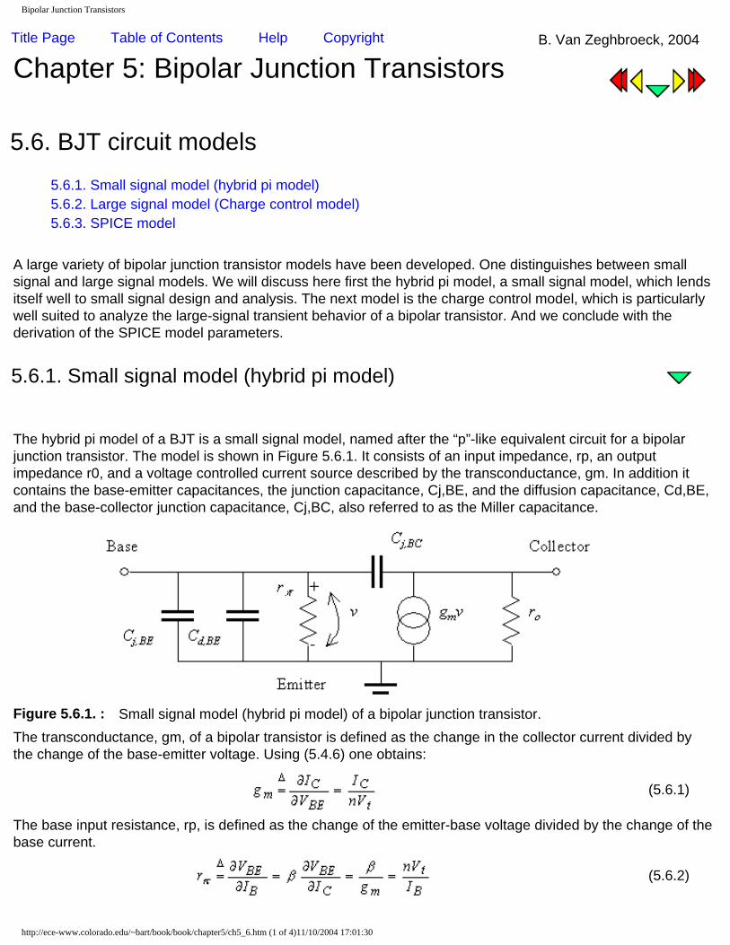
Bipolar Junction Transistors
Title Page Table of Contents Help Copyright B. Van Zeghbroeck, 2004
Chapter 5: Bipolar Junction Transistors
5.6. BJT circuit models5.6.1. Small signal model (hybrid pi model)5.6.2. Large signal model (Charge control model)5.6.3. SPICE model
A large variety of bipolar junction transistor models have been developed. One distinguishes between small signal and large signal models. We will discuss here first the hybrid pi model, a small signal model, which lends itself well to small signal design and analysis. The next model is the charge control model, which is particularly well suited to analyze the large-signal transient behavior of a bipolar transistor. And we conclude with the derivation of the SPICE model parameters.
5.6.1. Small signal model (hybrid pi model)
The hybrid pi model of a BJT is a small signal model, named after the “p”-like equivalent circuit for a bipolar junction transistor. The model is shown in Figure 5.6.1. It consists of an input impedance, rp, an output impedance r0, and a voltage controlled current source described by the transconductance, gm. In addition it contains the base-emitter capacitances, the junction capacitance, Cj,BE, and the diffusion capacitance, Cd,BE, and the base-collector junction capacitance, Cj,BC, also referred to as the Miller capacitance.
Figure 5.6.1. : Small signal model (hybrid pi model) of a bipolar junction transistor.The transconductance, gm, of a bipolar transistor is defined as the change in the collector current divided by the change of the base-emitter voltage. Using (5.4.6) one obtains:
(5.6.1)
The base input resistance, rp, is defined as the change of the emitter-base voltage divided by the change of the base current.
(5.6.2)
http://ece-www.colorado.edu/~bart/book/book/chapter5/ch5_6.htm (1 of 4)11/10/2004 17:01:30

Bipolar Junction Transistors
The output resistance, ro, is defined as:
(5.6.3)
The base-emitter and base-collector junction capacitances are given by:
(5.6.4)
(5.6.5)
for the case where the base-emitter and base-collector junctions are abrupt. Since the base-emitter is strongly forward biased in the forward active mode of operation, one has to also include the diffusion capacitance of the base:
(5.6.6)
Based on this small signal model shown in Figure 5.6.1, we can now calculate the small signal current gain of, hfe, of a BJT biased in the forward active mode and connected in a common emitter configuration as a function of frequency. The maximum current gain is calculated while shorting the output, resulting in:
(5.6.7)
The unity gain frequency, fT, also called the transit frequency is obtained by setting the small signal current gain, hfe, equals to one, resulting in:
(5.6.8)
This transit frequency can be expressed as a function of the transit time, t:
(5.6.9)
Where the transit time, t, equals:
(5.6.10)
The circuit model therefore includes the charging time of the base-emitter capacitance, tE, as well as the base transit time, tB, but not the transit time of the carriers through the base-collector depletion region, tC. The collector transit time was presented in Section 5.5.1. and described by equation (5.5.4), which is repeated here:
(5.6.11)
The total transit time then becomes:
http://ece-www.colorado.edu/~bart/book/book/chapter5/ch5_6.htm (2 of 4)11/10/2004 17:01:30

Bipolar Junction Transistors
(5.6.12)
The corresponding transit frequency, fT, can still be calculated using (5.6.9).While the unity gain frequency, fT, is an important figure of merit of a bipolar transistor, another even more important figure of merit is the maximum oscillation frequency, fMAX. This figure of merit predicts the unity power gain frequency and as a result indicates the maximum frequency at which useful power gain can be expected from a device. The maximum oscillation frequency, fMAX, is linked to the transit frequency, fT, and is obtained from:
(5.6.13)
Where RB is the total base resistance and Cj,BC is the base-collector capacitance. The total base resistance consists of the series connection of metal-semiconductor contact resistance, the resistance between the base contact metal and the emitter and the intrinsic base resistance. Assuming a base contact, which is longer than the penetration depth this base resistance equals
(5.6.14)
for a one-sided base contact, where Rs,c, Rs,BE and Rs are the sheet resistances under the base contact, between the base contact and the emitter and underneath the emitter respectively. Ls,E is the emitter stripe length of the emitter, Ws,E is the emitter stripe width of the emitter and DL is the alignment distance between the base contact and emitter. For a double-sided base contact, the total base resistance equals
(5.6.15)
The base-collector capacitance equals:
(5.6.16)
Where AC is the base-collector area.
5.6.2. Large signal model (Charge control model)
(5.6.17)(5.6.18)(5.6.19)(5.6.20)(5.6.21)(5.6.22)(5.6.23)(5.6.24)(5.6.25)(5.6.26)(5.6.27)
http://ece-www.colorado.edu/~bart/book/book/chapter5/ch5_6.htm (3 of 4)11/10/2004 17:01:30

Bipolar Junction Transistors
(5.6.28)
5.6.3. SPICE model
The SPICE model of a bipolar transistor includes a variety of parasitic circuit elements and some process related parameters in addition to the elements previously discussed in this chapter. The syntax of a bipolar transistor incorporates the parameters a circuit designer can change as shown below:
http://ece-www.colorado.edu/~bart/book/book/chapter5/ch5_6.htm (4 of 4)11/10/2004 17:01:30

5.7. Heterojunction Bipolar Transistors Heterojunction bipolar transistors are bipolar junction transistors, which are composed of at least two different semiconductors. As a result, the energy bandgap as well as all other material properties can be different in the emitter, base and collector. Moreover, a gradual change also called grading of the material is possible within each region.
Heterojunction bipolar transistors are not just an added complication. On the contrary, the use of heterojunctions provides an additional degree of freedom, which can result in vastly improved devices compared to the homojunction counterparts.
Figure 5.7.1. a) Flatband energy band diagram and b) Energy band diagram under forward active bias Variation of the minority-carrier distribution in the base quasi-neutral region due to a variation of the base-collector voltage.
The analysis of the device starts with the calculation of the DC current gain. To this end we recall the equations for the electron and hole current in the base-emitter junction (5.3.1) and (5.3.2), namely:
−
= 1)exp('
,2,,
t
BE
BB
BnEBinE V
VwN
DAqnI
(5.7.1)
and
−
= 1)exp('
,2,,
t
BE
EE
EpEEipE V
VwN
DAqnI
(5.7.2)
where the fact that the intrinsic carrier density in the emitter, ni,E, and base, ni,B, are different, is indicated explicitly by the additional subscript.
The emitter efficiency of the transistor is still calculated from the electron current relative to the
x
E
Ec
Ei
Ev
x
E
Ec
Ei
Ev
0-wE wB wB + wC
∆Ec
∆Ev
Emitter Base Collector Emitter Base Collector
0-wE wB wB + wC
x
E
Ec
Ei
Ev
x
E
Ec
Ei
Ev
0-wE wB wB + wC
∆Ec
∆Ev
Emitter Base Collector Emitter Base Collector
0-wE wB wB + wC

total emitter current and equals:
2,
',
2,
',,,
,
1
1
EiEEBn
BiBBEpnEpE
nEE
nwND
nwNDII
I
+
=+
=∆
γ (5.7.3)
If we now assume that the effective density of states for electrons and holes are the same in the emitter and base, we find that the maximum current gain equals:
E
g
BBEp
EEBn
kT
E
wNDwND
γαβ ≅∆
≅ if , )exp(',
',
(5.7.4)
Where ∆Eg is the difference between the bandgap energy in the emitter and the bandgap energy in the base. The current gain depends exponentially on this difference in bandgap energy. As a result one can obtain a very large current gain in a heterojunction bipolar transistor, even if the base doping density, NB, is significantly larger that the emitter doping density, NE. Therefore, the emitter of a typical heterojunction bipolar transistor has a wider bandgap than its base. This difference should be around 0.2 - 0.4 V for optimum performance. A smaller difference provides only a marginal improvement over homojunction devices. A larger difference causes the gain to be strongly temperature dependent, might require exotic material combinations and creates a distinct spike in the energy diagram, which in turn limits the current.
The advantages of HBTs are not restricted to its DC performance. Microwave devices can also be improved dramatically by using an appropriate heterojunction material system. To illustrate this point we now recall the equations for the transit frequency, fT, and the maximum oscillation frequency, fMAX:
τπ2
1=Tf
(5.7.5)
Where the total transit time equals:
sat
BCd
Bn
B
E
BEtCBE v
xDw
ICV
22,
.
2'
++=++= ττττ (5.7.6)
and
BCB
TMAX CR
ff
π2=
(5.7.7)
Since a heterojunction transistor can have large current gain, even if the base doping density is higher than the emitter doping density, the base can be much thinner even for the same punchthrough voltage. As a result one can reduce the base transit time without increasing the emitter charging time, while maintaining the same emitter current density. The transit frequency can be further improved by using materials with a higher mobility for the base layer and higher
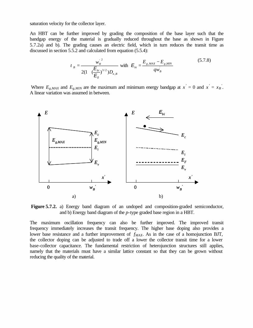
saturation velocity for the collector layer.
An HBT can be further improved by grading the composition of the base layer such that the bandgap energy of the material is gradually reduced throughout the base as shown in Figure 5.7.2a) and b). The grading causes an electric field, which in turn reduces the transit time as discussed in section 5.5.2 and calculated from equation (5.5.4):
Bnbi
BB
D
w
,2/3
2'
))(1(20E
E+
=τ with ',,
B
MINgMAXgbi qw
EE −=E
(5.7.8)
Where Eg,MAX and Eg,MIN are the maximum and minimum energy bandgap at x’ = 0 and x’ = xB’.
A linear variation was assumed in between.
a) b)
Figure 5.7.2. a) Energy band diagram of an undoped and composition-graded semiconductor, and b) Energy band diagram of the p-type graded base region in a HBT.
The maximum oscillation frequency can also be further improved. The improved transit frequency immediately increases the transit frequency. The higher base doping also provides a lower base resistance and a further improvement of fMAX. As in the case of a homojunction BJT, the collector doping can be adjusted to trade off a lower the collector transit time for a lower base-collector capacitance. The fundamental restriction of heterojunction structures still applies, namely that the materials must have a similar lattice constant so that they can be grown without reducing the quality of the material.
0 w B ’
x ’
E
E c
E F
E i
E v
E bi
0 w B ’
x ’
E
E c
E i
E v
E g ,MAX E g ,MIN
0 w B ’
x ’
E
E c
E F
E i
E v
E bi
0 w B ’
x ’
E
E c
E i
E v
E g ,MAX E g ,MIN

5.8. BJT Technology
5.8.1. First germanium BJT
The very first bipolar junction transistors were fabricated from a bar of germanium with two closely spaced alloyed contacts. Germanium was used since it could easily be purified to the extend that the minority carrier diffusion length was comparable to the distance between the two alloyed contacts. Starting with p-type germanium and using indium to form the alloyed junctions a discrete transistor was easily made. The germanium bar formed the base while the alloyed n-type regions formed the emitter and collector. Other implementations consisted of alloyed junctions on either side of a thin slice of germanium, with the emitter junction being smaller than the collector junction on the opposite side to ensure a high minority carrier collection efficiency on the collector side.
5.8.2. First silicon IC technology
This approach was soon abandoned and replaced by a double diffusion process, where the base and emitter region were formed by diffusion of dopants into the wafer. A low-doped collector region was epitaxially grown on the buried collector contact layer and isolation was obtained with a diffusion of opposite type. As similar process was also used to fabricate the first RTL (Resistor Transistor Logic) gates. It consists of the following steps:
Figure 5.8.1. Diffusion isolated bipolar junction transistor with load resistor
1. Grow low doped epilayer (p-type) 2. Diffuse collector contact layer (n-type) 3. Grow low doped collector layer (n-type) 4. Diffuse base region (p-type) 5. Diffuse emitter region (n-type) 6. Diffuse collector contact (n-type) 7. Diffuse device isolation (p-type) 8. Open via holes 9. Deposit contacts and wiring
This process yields n-p-n bipolar transistors. Resistors were formed using the p-type base diffusion. Resistor Transistor Logic (RTL) gates can thus be formed with this technology. The circuit and corresponding transfer characteristics are shown in Figure 5.8.2.
p substrate
nn+
Base/Input Emitter/Ground
n+p
Buried n+ layer
p+ p+p+
VCC
p
Collector/Output
p substrate
nn+
Base/Input Emitter/Ground
n+p
Buried n+ layer
p+ p+p+
VCC
p
Collector/Output

Figure 5.8.2. RTL inverter circuit and transfer characteristic
A lateral p-n-p transistor can also be fabricated with the same process. The device crosssection is shown in Figure 5.8.3.
Figure 5.8.3. Lateral p-n-p bipolar junction transistor
p substrate
nn+
Base Emitter
p
Buried n+ layer
p+pp
p+
Collector
p substrate
nn+
Base Emitter
p
Buried n+ layer
p+pp
p+
Collector
Vin
RL
Vin
IC
VBE
+-
VCC
+
-
VCC
Vout
Vout
Vin
RL
Vin
IC
VBE
+-
VCC
+
-
VCC
Vout
Vout

5.9. Bipolar Power Devices Power devices can be classified into bipolar-based devices, MOSFET-based devices and devices such as the IGBT that combine a bipolar transistor with a MOSFET.
Bipolar power devices are the traditional power devices because of their capability to provide high currents and high blocking voltages. The bipolar-based power devices include high-power bipolar transistors, Darlington transistors consisting of two transistors with a common collector, thyristors – also called silicon controlled rectifiers (SRCs) and triacs, a complementary thyristor structure suitable to control AC power.
Power MOSFETs and power devices that combine MOSFETs and bipolar transistors are covered in chapter 7.
5.9.1. Power BJTs
High power bipolar transistors are conceptually the same as the bipolar transistors described in chapter 8. The main difference is that the active area of the device is distinctly higher, resulting in a much higher current handling capability. Power BJTs also have a thick and low-doped collector region. Such collector regions result in a large blocking voltage. Extremely low doping densities, down to 1013 cm-3, are use to obtain blocking voltages as large as x000 V. As a result, one finds that the structure needs to be redesigned to a) effectively manage the power dissipation and b) avoid the Kirk effect.
The power dissipation is managed by minimizing the power dissipation and spreading the resulting heat dissipation onto a large area. The Kirk effect is normally avoided by increasing the collector doping density. However, for devices with a very high blocking voltage, this may not be an option. Power BJTs therefore are operated at rather low current density of 100 A/cm2 since the lower current density reduces the power dissipation per unit area and eliminates the Kirk effect. Large currents – up to 1000 A – are obtained by making a large area device. Silicon BJTs dominate the power device market, in part because of the low cost of large area silicon devices and the high thermal conductivity of silicon compared to GaAs. Silicon carbide (SiC) has been hailed as the perfect material for high-power BJTs. The higher thermal conductivity (3x) and breakdown field (10x) compared to silicon give it a clear performance advantage. The high saturation velocity (3x compared to silicon) also shifts the onset of the Kirk effect to higher current densities. The proliferation of its use will heavily depend on the material cost and quality of the SiC wafers.
5.9.2. Darlington Transistors
Darlington transistors contain two transistors connected in an emitter-follower configuration, while sharing the same collector contact. This structure can be fabricated with the same technology as a single BJT as shown in Figure 5.9.1. The key advantage of the Darlington configuration is that the total current gain of the circuit equals the product of the current gain of the two devices. The disadvantage is the larger saturation voltage. Since the two devices share the same collector, the saturation voltage of the Darlington pair equals the forward bias voltage of transistor Q2 plus the saturation voltage of transistor Q1. Since the forward bias voltage is much larger than the saturation voltage, the saturation voltage of the Darlington pair is also significantly larger. This larger voltage results in a larger on-state power dissipation in the device.

a) b)
Figure 5.9.1. Darlington transistor structure a) equivalent circuit b) device crosssection.
5.9.3. Silicon Controlled Rectifier (SRC) or Thyristor
The silicon controlled rectifier is 4-layer device with alternating n-type and p-type layers as shown in Figure 5.9.2. This devices is also referred to as a pnpn structure or Thyristor. Such device can in principle be made using any semiconductor. However, silicon thyristors are the most common thyristors. The advantage of the structure is that it provides a high power handling capability, high blocking voltage and high gain with a very low on-state resistance.
The operation of the device is best explained by considering the equivalent circuit, shown in Figure 5.9.2. It consists of two bipolar transistors, a n-p-n transistors, Q1, and a p-n-p transistor, Q2. Both transistors share a p-type and n-type layer. For instance, the p-type base layer of transistor Q1 is also the collector layer of transistor Q2, while the n-type base of transistor Q2 is also the collector of transistor Q1. The Thyristor is controlled by the gate electrode, which is the gate of Q1. By applying a current to the gate one forward biases the base-emitter junction of Q1, which leads to a collector current in Q1, which in turn provides a base current to Q2. Since Q2 is a complementary p-n-p transistor, this negative current also forward biases the base-emitter junction of transistor Q2, resulting in collector current which forms an additional base current into the base of transistor Q1. The applied current to the gate of the Thyristor therefore causes an additional current into Q1, which can be large enough that both transistors remain in turned on even if the original gate current is removed. This latching behavior is not unlike that of a flip-flop, where the inputs of two devices are connected to the output as shown in Figxxx. This self-sustaining effect will occur if the product of the current gain of both transistors equals unity, while one of the transistors can have a current gain less than unity. As a result one has considerable flexibility to choose the doping density and thickness of each of the layers to obtain a high blocking voltage and high Early voltage for each transistor, while maintaining sufficient current gain.
The Thyristor has a lower on-state voltage than the Darlington pair and typically requires an
n+ substrate
Collector
p n+
Base Emitter
n-
n+p
Base
Emitter
Collector
Q1
Q2
Q1 Q2
n+ substrate
Collector
p n+
Base Emitter
n-
n+p
Base
Emitter
Collector
Q1
Q2
Q1 Q2

even smaller turn-on current, which only needs to be applied temporarily because of the internal positive feedback between the two transistors of the equivalent circuit.
This latter property is also the main disadvantage of the Thyristor: since the device latches into the on-state once sufficient gate current is supplied, the device can not be turned off by removing the gate current. Instead one has to disconnect the power supply to turn off the device. Furthermore, since both transistors are in saturtion in the on-state, a significant amount of minority carriers are accumulated in the base region of each transistor. These minority carriers must be remove prior to reconnecting the power supply since these carriers would temporarily lead to a base current in each device and trigger the turn-o of the Thyristor. Finally, one has to slowly ramp up the power supply voltage to avoid the so-called dV/dt effect. Since a rapid increase of the applied voltage with time causes a displacement current proportional to the capacitance of the junctions, this displacement current could again provide a temporary base current in Q1 and Q2, which is large enough to trigger the Thyristor.
Figure 5.9.2. Thyristor structure: a) circuit symbol, b) device cross-section and c) equivalent circuit.
A very attractive feature of a Thyristor is that it can be scaled easily to very large area devices even if that causes a significant lateral resistance though the thin and lowly-doped base and collector regions. As one applies a current to the gate electrode, the Thyristor would be triggered locally. The turned-on region would then spread laterally thoughout the structure without a need for an additional gate current. The local triggering also exists in the light-controlled Thyristor. This structure does not contain a gate electrode. Instead the p-n-p-n structure is locally illuminated with photons whose energy exceeds the bandgap energy of the semiconductor. The photogenerated current then acts as the gate current, which triggers the Thyristor.
Gate turn-off Thyristor (GTO)
5.9.4. DIode and TRiode AC Switch (DIAC and TRIAC)
The diode AC switch and the triode AC switch are very similar to the thyristors, since they both are latching multi-layer device structures. Both are meant to be used in AC powered systems and therefore respond similarly to positive and negative applied voltages. The circuit symbols and layer structures are shown for both devices in Figure 5.9.3. The diode AC switch also referred to
Anode
p
n+
Gate
n
p+ substrate
Cathode
p+
Gate
Anode Cathode
Anode
Cathode
Q1
Q2
Gate
Q1
Q2
Anode
p
n+
Gate
n
p+ substrate
Cathode
p+
Gate
Anode Cathode
Anode
Cathode
Q1
Q2
Gate
Q1
Q2

as DIAC consists of a gate-less pnpn structure connected in parallel to a gate-less npnp structure. This device therefore acts like an open circuit until the threshold voltage is reached - either positive or negative – after which the device acts as a short. To achieve this function one starts with a pnp structure. An n+ region is added to the front and the back to yield the DIAC structure.
The triode AC switch (TRIAC) also contains the same vertical structure as a DIAC. In addition a contact is made to the p-type gate of the npnp structure as well as the n-type gate of the pnpn structure. This additional gate contact allows lowering the threshold for latching for both positive and negative applied voltages applied between terminal 1 and terminal 2.
Figure 5.9.3. Circuit symbol and device cross-section of a) a Diode AC switch (DIAC) and b) a Triode AC switch (TRIAC).
Terminal 2
pn+
Gate
n
n+p
Terminal 1
n+
Gate
Terminal 1 Terminal 2
Terminal 2
pn+
n
n+p
Terminal 1
Terminal 1 Terminal 2
Terminal 2
pn+
Gate
n
n+p
Terminal 1
n+
Gate
Terminal 1 Terminal 2
Terminal 2
pn+
n
n+p
Terminal 1
Terminal 1 Terminal 2

example 3
Title Page Table of Contents Help Copyright B. Van Zeghbroeck, 2004
Chapter 5: Bipolar Junction Transistors
Examples
Example 5.1 A bipolar transistor with an emitter current of 1 mA has an emitter efficiency of 0.99, a base transport factor of 0.995 and a depletion layer recombination factor of 0.998. Calculate the base current, the collector current, the transport factor and the current gain of the transistor.
Example 5.2 Consider a pnp bipolar transistor with emitter doping of 1018 cm-3 and base doping of 1017 cm-3. The quasi-neutral region width in the emitter is 1 µm and 0.2 µm in the base. Use µn = 1000 cm2/V-s and µp = 300 cm2/V-s . The minority carrier lifetime in the base is 10 ns.Calculate the emitter efficiency, the base transport factor, and the current gain of the transistor biased in the forward active mode. Assume there is no recombination in the depletion region.
Example 5.3 Calculate the saturation voltage of a bipolar transistor biased with a base current of 1 mA and a collector current of 10 mA. Use αR = 0.993 and αF = 0.2.
Example 5.4 Consider a bipolar transistor with a base doping of 1017 cm-3 and a quasi-neutral base width of 0.2 µm. Calculate the Early voltage and collector current ideality factor given that the base-emitter capacitance and the base-collector capacitance are 0.2 nF and 0.2 pF. The collector area equals 10-4 cm-2.
http://ece-www.colorado.edu/~bart/book/book/chapter5/ch5_ex.htm11/10/2004 17:04:58

Example 5.1 A bipolar transistor with an emitter current of 1 mA has an emitter efficiency of 0.99, a base transport factor of 0.995 and a depletion layer recombination factor of 0.998. Calculate the base current, the collector current, the transport factor and the current gain of the transistor.
Solution The transport factor and current gain are: 983.0998.0995.099.0 =××== rTE δαγα
and
1.581
=−
=α
αβ
The collector current then equals
mA 0.983== EC II α And the base current is obtained from:
µA 17=−= CEB III

Example 5.2 Consider a pnp bipolar transistor with emitter doping of 1018 cm-3
and base doping of 1017 cm-3. The quasi-neutral region width in the emitter is 1 µm and 0.2 µm in the base. Use µn = 1000 cm2/V-s and µp = 300 cm2/V-s . The minority carrier lifetime in the base is 10 ns. Calculate the emitter efficiency, the base transport factor, and the current gain of the transistor biased in the forward active mode. Assume there is no recombination in the depletion region.
Solution The emitter efficiency is obtained from:
994.0
1
1
',
',
=
+
=
EEBn
BBEpE
wND
wNDγ
The base transport factor equals:
9992.02
1,
2'=−=
nBn
BT D
wτ
α
The current gain then becomes:
5.1471
=−
=α
αβ
where the transport factor, α, was calculated as the product of the emitter efficiency and the base transport factor:
993.09992.0994.0 =×== TE αγα

Example 5.3 Calculate the saturation voltage of a bipolar transistor biased with a base current of 1 mA and a collector current of 10 mA. Use αR = 0.993 and αF = 0.2.
Solution The saturation voltage equals:
V 0.1)1(
1
)1(1ln, =
−−
−+=
F
F
B
CR
RB
C
tsatCE
II
II
VV
αα
α
α

Example 5.4 Consider a bipolar transistor with a base doping of 1017 cm-3 and a quasi-neutral base width of 0.2 µm. Calculate the Early voltage and collector current ideality factor given that the base-emitter capacitance and the base-collector capacitance are 0.2 nF and 0.2 pF. The collector area equals 10-4 cm-2.
Solution The Early voltage equals:
V160,
'
,===
BCj
BBC
BCj
BA C
wNqAC
QV
The saturation voltage equals:
16.11 , =+≅ BEjB
t CQV
n

http://ece-www.colorado.edu/~bart/book/book/chapter5/ch5_p.htm
Title Page Table of Contents Help Copyright B. Van Zeghbroeck, 2004
Chapter 5: Bipolar Junction Transistors
Problems
1. A silicon npn bipolar transistor with NE = 1018 cm-3, NB = 1017 cm-3 and NC = 1016 cm-3, wE = 1 µm, wB = 0.5 µm , and wC = 4 µm is biased with VBE = 0.6 V and VCB = 0 V. Use µn = 1000 cm2/V-s, µp = 300 cm2/V-s and τn = τp = 100 ns. The emitter area equals 10-4 cm2.
a. Calculate the width of the quasi-neutral regions in the emitter, base and collector. b.
Calculate the minority-carrier diffusion lengths in the emitter, base and collector. Calculate the ratio of the minority-carrier diffusion length and the quasi-neutral region width in each region.
c. Calculate the excess-minority-carrier charge density per unit area in the emitter, base and collector.
d. Calculate the emitter current while ignoring the recombination in the depletion region.
e. Calculate the base transit time and the current due to recombination of electrons in the base.
f. Calculate the emitter efficiency and the base transport factor.
g. Calculate the emitter efficiency and the base transport factor.
h. Calculate the transport factor and the current gain assuming there is no recombination in the depletion regions.
i. Calculate the collector capacitance, the majority-carrier charge density in the base and the Early voltage.
A silicon npn bipolar transistor has an emitter doping, NE = 2 x1018 cm-3, an emitter width wE = 1 µm, and a base doping of 2 x 1017 cm-3. A current gain of 100 and an early voltage of 100 V is desired. Using µn = 1000 cm2/V-s, µp = 300 cm2/V-s and τn = τp = 100 ns, find the corresponding base width and base doping. The emitter area equals 10-4 cm2.
http://ece-www.colorado.edu/~bart/book/book/chapter5/ch5_p.htm11/10/2004 17:05:26

http://ece-www.colorado.edu/~bart/book/book/chapter5/ch5_r.htm
Title Page Table of Contents Help Copyright B. Van Zeghbroeck, 2004
Chapter 5: Bipolar Junction Transistors
Review Questions
1. Describe the motion of electrons and holes in a pnp bipolar transistor biased in the forward active mode with VBC = 0.
2. What is the definition of the emitter efficiency? Explain in words and provide the corresponding equation.
3. What is the definition of the base transport factor? Explain in words and provide the corresponding equation.
4. Derive the relation between the current gain and the transport factor.
5. How does recombination in the quasi-neutral base region affect the emitter, base and collector current?
6. How does recombination in the base-emitter depletion region affect the emitter, base and collector current?
7. Explain the four different bias modes of a bipolar transistor.
8. Explain why a transistor can have a current gain larger than one in the common emitter mode. Provide the necessary and sufficient conditions needed to obtain a current gain larger than one.
9. What is the Early effect and how does it affect the transistor characteristics?
http://ece-www.colorado.edu/~bart/book/book/chapter5/ch5_r.htm11/10/2004 17:05:34

Chapter 5 Bibliography
Title Page Table of Contents Help Copyright B. Van Zeghbroeck, 2004
Chapter 5: Bipolar Junction Transistors
Bibliography
1. A. Barlev, "Semiconductor and Electronic Devices": Prentice Hall, Third edition, 1992.
2. H. C. Casey, jr., "Devices For Integrated Circuits": John Wiley & Sons, 1999.
3. D. A. Neaman, "Semiconductor Physics and Devices, Second Edition": Irwin, 1997.
4. G. W. Neudeck, "The Bipolar Junction Transistor": Addison-Wesley, 1983.
5. R. F. Pierret, "Semiconductor Device Fundamentals": Addison-Wesley, 1996.
6. D. L. Pulfrey and N. G. Tarr, "Introduction of Microelectronic Devices": Prentice Hall, 1989.
7. D. J. Roulston, "An Introduction to the Physics of Semiconductor Devices": Oxford, 1999.
8. M. Shur, "Physics of Semiconductor Devices": Prentice Hall, 1990.
9. J. Singh, "Semiconductor Devices": John Wiley & Sons, 2001.
10. B. G. Streetman and S. Banerjee, "Solid State Electronic Devices, Fifth Edition": Prentice Hall, 2000.
11. S. M. Sze, "Physics of Semiconductor Devices, Second Edition": John Wiley & Sons, 1981.
12. S. Wang, "Fundamentals of Semiconductor Theory and Device Physics": Prentice Hall, 1989.
http://ece-www.colorado.edu/~bart/book/book/chapter5/ch5_b.htm11/10/2004 17:05:41

Chapter 5 Equations
Title Page Table of Contents Help Copyright B. Van Zeghbroeck, 2004
Chapter 5: Bipolar Junction Transistors
Equations
(5.2.1)
(5.2.2)
(5.2.3)
(5.2.4)
(5.2.5)
(5.2.6)
(5.2.7)
(5.2.8)
http://ece-www.colorado.edu/~bart/book/book/chapter5/ch5_eq.htm (1 of 5)11/10/2004 17:05:47

Chapter 5 Equations
(5.2.9)
(5.2.10)
(5.2.11)
(5.2.12)
(5.2.13)
(5.2.14)
(5.2.15)
(5.2.16)
(5.2.17)
(5.2.18)
http://ece-www.colorado.edu/~bart/book/book/chapter5/ch5_eq.htm (2 of 5)11/10/2004 17:05:47

Chapter 5 Equations
(5.2.19)
(5.2.20)
(5.3.1)
(5.3.2)
(5.3.3)
(5.3.4)
(5.3.5)
(5.3.6)
(5.3.7)
(5.3.8)
http://ece-www.colorado.edu/~bart/book/book/chapter5/ch5_eq.htm (3 of 5)11/10/2004 17:05:47

Chapter 5 Equations
(5.3.9)
(5.3.10)
(5.3.11)
(5.3.12)
(5.3.13)
(5.3.14)
(5.3.15)
(5.3.16)
(5.3.17)
(5.3.18)
http://ece-www.colorado.edu/~bart/book/book/chapter5/ch5_eq.htm (4 of 5)11/10/2004 17:05:47

Chapter 5 Equations
(5.3.19)
(5.3.20)
(5.4.1)
(5.4.2)
(5.4.3)
(5.4.4)
http://ece-www.colorado.edu/~bart/book/book/chapter5/ch5_eq.htm (5 of 5)11/10/2004 17:05:47

MOS Capacitors
Title Page Table of Contents Help Copyright B. Van Zeghbroeck, 2004
Chapter 6: MOS Capacitors
6.1. Introduction
The primary reason to study the Metal-Oxide-Silicon (MOS) capacitor is to understand the principle of operation as well as the detailed analysis of the Metal-Oxide-Silicon Field Effect Transistor (MOSFET). In this chapter, we introduce the MOS structure and its four different modes of operation, namely accumulation, flatband, depletion and inversion. We then consider the flatband voltage in more detail and present the MOS analysis based on the full depletion approximation. Finally, we analyze and discuss the MOS capacitance.
http://ece-www.colorado.edu/~bart/book/book/chapter6/ch6_1.htm11/10/2004 17:06:28
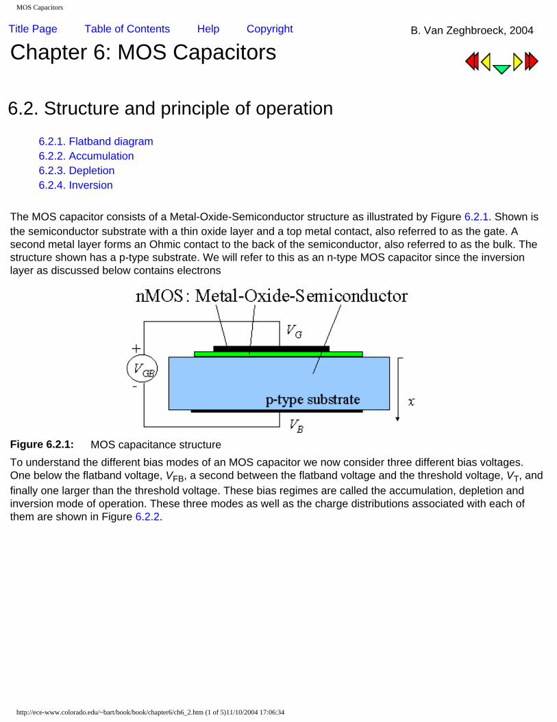
MOS Capacitors
Title Page Table of Contents Help Copyright B. Van Zeghbroeck, 2004
Chapter 6: MOS Capacitors
6.2. Structure and principle of operation6.2.1. Flatband diagram 6.2.2. Accumulation6.2.3. Depletion6.2.4. Inversion
The MOS capacitor consists of a Metal-Oxide-Semiconductor structure as illustrated by Figure 6.2.1. Shown is the semiconductor substrate with a thin oxide layer and a top metal contact, also referred to as the gate. A second metal layer forms an Ohmic contact to the back of the semiconductor, also referred to as the bulk. The structure shown has a p-type substrate. We will refer to this as an n-type MOS capacitor since the inversion layer as discussed below contains electrons
Figure 6.2.1: MOS capacitance structureTo understand the different bias modes of an MOS capacitor we now consider three different bias voltages. One below the flatband voltage, VFB, a second between the flatband voltage and the threshold voltage, VT, and finally one larger than the threshold voltage. These bias regimes are called the accumulation, depletion and inversion mode of operation. These three modes as well as the charge distributions associated with each of them are shown in Figure 6.2.2.
http://ece-www.colorado.edu/~bart/book/book/chapter6/ch6_2.htm (1 of 5)11/10/2004 17:06:34

MOS Capacitors
Figure 6.2.2.: Charges in a Metal-Oxide-Semiconductor structure under accumulation, depletion and inversion conditions
Accumulation occurs typically for negative voltages where the negative charge on the gate attracts holes from the substrate to the oxide-semiconductor interface. Depletion occurs for positive voltages. The positive charge on the gate pushes the mobile holes into the substrate. Therefore, the semiconductor is depleted of mobile carriers at the interface and a negative charge, due to the ionized acceptor ions, is left in the space charge region. The voltage separating the accumulation and depletion regime is referred to as the flatband voltage, VFB. Inversion occurs at voltages beyond the threshold voltage. In inversion, there exists a negatively charged inversion layer at the oxide-semiconductor interface in addition to the depletion-layer. This inversion layer is due to minority carriers, which are attracted to the interface by the positive gate voltage.The energy band diagram of an n-MOS capacitor biased in inversion is shown in Figure 6.2.3. The oxide is characterized as a semiconductor with a very large bandgap, which blocks any flow of carriers between the semiconductor and the gate metal. The band-bending in the semiconductor is consistent with the presence of a depletion layer. At the semiconductor-oxide interface, the Fermi energy is close to the conduction band edge as expected when a high density of electrons is present. An interesting point to note is that as the oxide behaves as an ideal insulator, the semiconductor is in thermal equilibrium even when a voltage is applied to the gate. The presence of an electric field does not automatically lead to a non-equilibrium condition, as was also the case for a p-n diode with zero bias.
http://ece-www.colorado.edu/~bart/book/book/chapter6/ch6_2.htm (2 of 5)11/10/2004 17:06:34

MOS Capacitors
Figure 6.2.3: Energy band diagram of an MOS structure biased in inversion.We will discuss in the next sections the four modes of operation of an MOS structure: Flatband, Depletion, Inversion and Accumulation. Flatband conditions exist when no charge is present in the semiconductor so that the silicon energy band is flat. Initially we will assume that this occurs at zero gate bias. Later we will consider the actual flat band voltage in more detail. Surface depletion occurs when the holes in the substrate are pushed away by a positive gate voltage. A more positive voltage also attracts electrons (the minority carriers) to the surface, which form the so-called inversion layer. Under negative gate bias, one attracts holes from the p-type substrate to the surface, yielding accumulation.
6.2.1. Flatband diagram
The flatband diagram is by far the easiest energy band diagram. The term flatband refers to fact that the energy band diagram of the semiconductor is flat, which implies that no charge exists in the semiconductor. The flatband diagram of an aluminum-silicon dioxide-silicon MOS structure is shown in Figure 6.2.4. Note that a voltage, VFB, must be applied to obtain this flat band diagram. Indicated on the figure is also the work function of the aluminum gate, ΦM, the electron affinity of the oxide, χoxide, and that of silicon, χ, as well as the bandgap energy of silicon, Eg. The bandgap energy of the oxide is quoted in the literature to be between 8 and 9 electron volt. The reader should also realize that the oxide is an amorphous material and the use of semiconductor parameters for such material can justifiably be questioned. The flat band voltage is obtained when the applied gate voltage equals the workfunction difference between the gate metal and the semiconductor. If there is also a fixed charge in the oxide and/or at the oxide-silicon interface, the expression for the flatband voltage must be modified accordingly.
http://ece-www.colorado.edu/~bart/book/book/chapter6/ch6_2.htm (3 of 5)11/10/2004 17:06:34

MOS Capacitors
Figure 6.2.4: Flatband energy diagram of a metal-oxide-semiconductor (MOS) structure consisting of an aluminum metal, silicon dioxide and silicon.
6.2.2. Accumulation
Accumulation occurs when one applies a voltage, which is less than the flatband voltage. The negative charge on the gate attracts holes from the substrate to the oxide-semiconductor interface. Only a small amount of band bending is needed to build up the accumulation charge so that almost all of the potential variation is within the oxide.
6.2.3. Depletion
As a more positive voltage than the flatband voltage is applied, a negative charge builds up in the semiconductor. Initially this charge is due to the depletion of the semiconductor starting from the oxide-semiconductor interface. The depletion layer width further increases with increasing gate voltage.
6.2.4. Inversion
As the potential across the semiconductor increases beyond twice the bulk potential, another type of negative charge emerges at the oxide-semiconductor interface: this charge is due to minority carriers, which form a so-called inversion layer. As one further increases the gate voltage, the depletion layer width barely increases further since the charge in the inversion layer increases exponentially with the surface potential.
http://ece-www.colorado.edu/~bart/book/book/chapter6/ch6_2.htm (4 of 5)11/10/2004 17:06:34
MOS Capacitors
http://ece-www.colorado.edu/~bart/book/book/chapter6/ch6_2.htm (5 of 5)11/10/2004 17:06:34

MOS analysis
Title Page Table of Contents Help Copyright B. Van Zeghbroeck, 2004
Chapter 6: MOS Capacitors
6.3. MOS analysis6.3.1. Flatband voltage calculation6.3.2. Inversion layer charge6.3.3. Full depletion analysis6.3.4. MOS Capacitance
6.3.1. Flatband voltage calculation
If there is no charge present in the oxide or at the oxide-semiconductor interface, the flat band voltage simply equals the difference between the gate metal workfunction, ΦM, and the semiconductor workfunction, ΦS.
(6.3.1)
The workfunction is the voltage required to extract an electron from the Fermi energy to the vacuum level. This voltage is between three and five Volt for most metals. It should be noted that the actual value of the workfunction of a metal deposited onto silicon dioxide is not exactly the same as that of the metal in vacuum. Figure 6.3.1 provides experimental values for the workfunction of different metals as obtained from a measurement of a MOS capacitor as a function of the measured workfunction in vacuum. The same data is also listed in Table 6.3.1.
Figure 6.3.1.: Workfunction of Magnesium (Mg), Aluminum (Al), Copper (Cu), Silver (Ag), Nickel (Ni) and Gold (Au) obtained from I-V and C-V measurements on MOS structures as a function of the workfunction of those metals measured in vacuum.
http://ece-www.colorado.edu/~bart/book/book/chapter6/ch6_3.htm (1 of 13)11/10/2004 17:06:48

MOS analysis
Table 6.3.1: Workfunction of selected metals as measured in vacuum and as obtained from a C-V measurement on an MOS structure.
The workfunction of a semiconductor, ΦS, requires some more thought since the Fermi energy varies with the doping type as well as with the doping concentration. This workfunction equals the sum of the electron affinity in the semiconductor, χ, the difference between the conduction band energy and the intrinsic energy divided by the electronic charge and the bulk potential as expressed by the following equation:
(6.3.2)
For MOS structures with a highly doped poly-silicon gate one must also calculate the workfunction of the gate based on the bulk potential of the poly-silicon.
(6.3.3)
Where Na,poly and Nd,poly are the acceptor and donor density of the p-type and n-type poly-silicon gate respectively. The flatband voltage of real MOS structures is further affected by the presence of charge in the oxide or at the oxide-semiconductor interface. The flatband voltage still corresponds to the voltage, which, when applied to the gate electrode, yields a flat energy band in the semiconductor. The charge in the oxide or at the interface changes this flatband voltage. For a charge, Qi, located at the interface between the oxide and the semiconductor, and a charge density, ρox, distributed within the oxide, the flatband voltage is given by:
(6.3.4)
where the second term is the voltage across the oxide due to the charge at the oxide-semiconductor interface and the third term is due to the charge density in the oxide. The actual calculation of the flatband voltage is further complicated by the fact that charge can move within the oxide. The charge at the oxide-semiconductor interface due to surface states also depends on the position of the Fermi energy. Since any additional charge affects the flatband voltage and thereby the threshold voltage, great care has to be taken during fabrication to avoid the incorporation of charged ions as well as creation of surface states. Example 6.1 Calculate the flatband voltage of a silicon nMOS capacitor with a substrate doping Na = 1017
cm-3 and an aluminum gate (ΦM = 4.1 V). Assume there is no fixed charge in the oxide or at the oxide-silicon interface.
http://ece-www.colorado.edu/~bart/book/book/chapter6/ch6_3.htm (2 of 13)11/10/2004 17:06:48

MOS analysis
Solution The flatband voltage equals the work function difference since there is no charge in the oxide or at the oxide-semiconductor interface.
The flatband voltages for nMOS and pMOS capacitors with an aluminum or a poly-silicon gate are listed in the table below.
6.3.2. Inversion layer charge
The basis assumption as needed for the derivation of the MOSFET models is that the inversion layer charge is proportional with the applied voltage. In addition, the inversion layer charge is zero at and below the threshold voltage as described by:
(6.3.5)
The linear proportionality can be explained by the fact that a gate voltage variation causes a charge variation in the inversion layer. The proportionality constant between the charge and the applied voltage is therefore expected to be the gate oxide capacitance. This assumption also implies that the inversion layer charge is located exactly at the oxide-semiconductor interface.Because of the energy band gap of the semiconductor separating the electrons from the holes, the electrons can only exist if the p-type semiconductor is first depleted. The voltage at which the electron inversion-layer forms is referred to as the threshold voltage. To justify this assumption we now examine a comparison of a numeric solution with equation (6.3.4) as shown in Figure 6.3.2.
http://ece-www.colorado.edu/~bart/book/book/chapter6/ch6_3.htm (3 of 13)11/10/2004 17:06:48

MOS analysis
Figure 6.3.2.: Charge density due to electrons in the inversion layer of an MOS capacitor. Compared are the analytic solution (solid line) and equation (6.3.5) (dotted line) for Na = 1017 cm-3 and tox = 20 nm.
While there is a clear difference between the curves, the difference is small. We will therefore use our basic assumption when deriving the different MOSFET models since it dramatically simplifies the derivation, be it while losing some accuracy.
6.3.3. Full depletion analysis
We now derive the MOS parameters at threshold with the aid of Figure 6.3.3. To simplify the analysis we make the following assumptions: 1) we assume that we can use the full depletion approximation and 2) we assume that the inversion layer charge is zero below the threshold voltage. Beyond the threshold voltage we assume that the inversion layer charge changes linearly with the applied gate voltage. The derivation starts by examining the charge per unit area in the depletion layer, Qd. As can be seen in Figure 6.3.3 (a), this charge is given by:
(6.3.6)
Where xd is the depletion layer width and Na is the acceptor density in the substrate. Integration of the charge density then yields the electric field distribution shown in Figure 6.3.3 (b). The electric field in the semiconductor at the interface, s, and the field in the oxide equal, ox:
(6.3.7)
http://ece-www.colorado.edu/~bart/book/book/chapter6/ch6_3.htm (4 of 13)11/10/2004 17:06:48
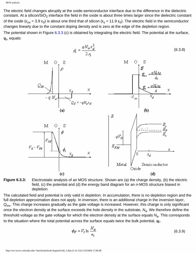
MOS analysis
The electric field changes abruptly at the oxide-semiconductor interface due to the difference in the dielectric constant. At a silicon/SiO2 interface the field in the oxide is about three times larger since the dielectric constant of the oxide (εox = 3.9 ε0) is about one third that of silicon (εs = 11.9 ε0). The electric field in the semiconductor changes linearly due to the constant doping density and is zero at the edge of the depletion region.The potential shown in Figure 6.3.3 (c) is obtained by integrating the electric field. The potential at the surface, φs, equals:
(6.3.8)
Figure 6.3.3: Electrostatic analysis of an MOS structure. Shown are (a) the charge density, (b) the electric field, (c) the potential and (d) the energy band diagram for an n-MOS structure biased in depletion.
The calculated field and potential is only valid in depletion. In accumulation, there is no depletion region and the full depletion approximation does not apply. In inversion, there is an additional charge in the inversion layer, Qinv. This charge increases gradually as the gate voltage is increased. However, this charge is only significant once the electron density at the surface exceeds the hole density in the substrate, Na. We therefore define the threshold voltage as the gate voltage for which the electron density at the surface equals Na. This corresponds to the situation where the total potential across the surface equals twice the bulk potential, φF.
(6.3.9)
http://ece-www.colorado.edu/~bart/book/book/chapter6/ch6_3.htm (5 of 13)11/10/2004 17:06:48

MOS analysis
The depletion layer in depletion is therefore restricted to this potential range:
(6.3.10)
For a surface potential larger than twice the bulk potential, the inversion layer charge change increases exponentially with the surface potential. Consequently, an increased gate voltage yields an increased voltage across the oxide while the surface potential remains almost constant. We will therefore assume that the surface potential and the depletion layer width at threshold equal those in inversion. The corresponding expressions for the depletion layer charge at threshold, Qd,T, and the depletion layer width at threshold, xd,T, are:
(6.3.11)
(6.3.12)
Beyond threshold, the total charge in the semiconductor has to balance the charge on the gate electrode, QM, or:
(6.3.13)
where we define the charge in the inversion layer as a quantity which needs to determined but should be consistent with our basic assumption. This leads to the following expression for the gate voltage, VG:
(6.3.14)
In depletion, the inversion layer charge is zero so that the gate voltage becomes:
(6.3.15)
while in inversion this expression becomes:
(6.3.16)
the third term in (6.3.16) states our basic assumption, namely that any change in gate voltage beyond the threshold requires a change of the inversion layer charge. From the second equality in equation (6.3.16), we then obtain the threshold voltage or:
(6.3.17)
Example 6.2 Calculate the threshold voltage of a silicon nMOS capacitor with a substrate doping Na = 1017 cm-3, a 20 nm thick oxide (εox = 3.9 ε0) and an aluminum gate (ΦM = 4.1 V). Assume there is no fixed charge in the oxide or at the oxide-silicon interface.
http://ece-www.colorado.edu/~bart/book/book/chapter6/ch6_3.htm (6 of 13)11/10/2004 17:06:48
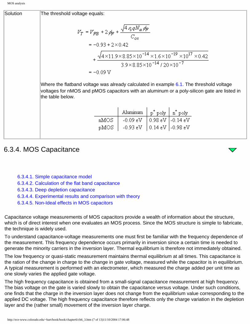
MOS analysis
Solution The threshold voltage equals:
Where the flatband voltage was already calculated in example 6.1. The threshold voltage voltages for nMOS and pMOS capacitors with an aluminum or a poly-silicon gate are listed in the table below.
6.3.4. MOS Capacitance
6.3.4.1. Simple capacitance model6.3.4.2. Calculation of the flat band capacitance6.3.4.3. Deep depletion capacitance6.3.4.4. Experimental results and comparison with theory6.3.4.5. Non-Ideal effects in MOS capacitors
Capacitance voltage measurements of MOS capacitors provide a wealth of information about the structure, which is of direct interest when one evaluates an MOS process. Since the MOS structure is simple to fabricate, the technique is widely used. To understand capacitance-voltage measurements one must first be familiar with the frequency dependence of the measurement. This frequency dependence occurs primarily in inversion since a certain time is needed to generate the minority carriers in the inversion layer. Thermal equilibrium is therefore not immediately obtained. The low frequency or quasi-static measurement maintains thermal equilibrium at all times. This capacitance is the ration of the change in charge to the change in gate voltage, measured while the capacitor is in equilibrium. A typical measurement is performed with an electrometer, which measured the charge added per unit time as one slowly varies the applied gate voltage. The high frequency capacitance is obtained from a small-signal capacitance measurement at high frequency. The bias voltage on the gate is varied slowly to obtain the capacitance versus voltage. Under such conditions, one finds that the charge in the inversion layer does not change from the equilibrium value corresponding to the applied DC voltage. The high frequency capacitance therefore reflects only the charge variation in the depletion layer and the (rather small) movement of the inversion layer charge.
http://ece-www.colorado.edu/~bart/book/book/chapter6/ch6_3.htm (7 of 13)11/10/2004 17:06:48

MOS analysis
In this section, we first derive the simple capacitance model, which is based on the full depletion approximation and our basic assumption. The comparison with the exact low frequency capacitance will reveal that the largest error occurs at the flatband voltage. We therefore derive the exact flatband capacitance using the linearized Poisson's equation. Then we discuss the full exact analysis followed by a discussion of deep depletion as well as the non-ideal effects in MOS capacitors.
6.3.4.1. Simple capacitance model
The capacitance of an MOS capacitor is obtained using the same assumptions as those listed in section 6.3.3. The MOS structure is treated as a series connection of two capacitors: the capacitance of the oxide and the capacitance of the depletion layer. In accumulation, there is no depletion layer. The remaining capacitor is the oxide capacitance, so that the capacitance equals:
(6.3.18)
In depletion, the MOS capacitance is obtained from the series connection of the oxide capacitance and the capacitance of the depletion layer, or:
(6.3.19)
where xd is the variable depletion layer width which is calculated from:
(6.3.20)
In order to find the capacitance corresponding to a specific value of the gate voltage we also need to use the relation between the potential across the depletion region and the gate voltage, given by:
(6.3.15)
In inversion, the capacitance becomes independent of the gate voltage. The low frequency capacitance equals the oxide capacitance since charge is added to and removed from the inversion layer. The high frequency capacitance is obtained from the series connection of the oxide capacitance and the capacitance of the depletion layer having its maximum width, xd,T. The capacitances are given by:
(6.3.21)
The capacitance of an MOS capacitor as calculated using the simple model is shown in Figure 6.3.4. The dotted lines represent the simple model while the solid line corresponds to the low frequency capacitance as obtained from the exact analysis.
http://ece-www.colorado.edu/~bart/book/book/chapter6/ch6_3.htm (8 of 13)11/10/2004 17:06:48

MOS analysis
Figure 6.3.4 : Low frequency capacitance of an nMOS capacitor. Shown are the exact solution for the low frequency capacitance (solid line) and the low and high frequency capacitance obtained with the simple model (dotted lines). Na = 1017 cm-3 and tox = 20 nm.
6.3.4.2. Calculation of the flat band capacitance
The simple model predicts that the flatband capacitance equals the oxide capacitance. However, the comparison with the exact solution of the low frequency capacitance as shown in Figure 6.3.4 reveals that the error can be substantial. The reason for this is that we have ignored any charge variation in the semiconductor. We will therefore now derive the exact flatband capacitance. To derive the flatband capacitance including the charge variation in the semiconductor, we first linearize Poisson's equation. Since the potential across the semiconductor at flatband is zero, we expect the potential to be small as we vary the gate voltage around the flatband voltage. Poisson's equation can then be simplified to:
(6.3.22)
Charge due to ionized donors or electrons were eliminated, since neither are present in a p-type semiconductor around flatband. The linearization is obtained by replacing the exponential function by the first two terms of its Taylor series expansion. The solution to this equation is:
(6.3.23)
Where fs is the potential at the surface of the semiconductor and LD is called the Debye length. The solution of the potential enables the derivation of the capacitance of the semiconductor under flatband conditions, or:
(6.3.24)
http://ece-www.colorado.edu/~bart/book/book/chapter6/ch6_3.htm (9 of 13)11/10/2004 17:06:48

MOS analysis
The flatband capacitance of the MOS structure at flatband is obtained by calculating the series connection of the oxide capacitance and the capacitance of the semiconductor, yielding:
(6.3.25)
Example 6.3 Calculate the oxide capacitance, the flatband capacitance and the high frequency capacitance in inversion of a silicon nMOS capacitor with a substrate doping Na = 1017 cm-3, a 20 nm thick oxide (εox = 3.9 ε0) and an aluminum gate (ΦM = 4.1 V).
Solution The oxide capacitance equals:
The flatband capacitance equals:
where the Debye length is obtained from:
The high frequency capacitance in inversion equals:
and the depletion layer width at threshold equals:
http://ece-www.colorado.edu/~bart/book/book/chapter6/ch6_3.htm (10 of 13)11/10/2004 17:06:48
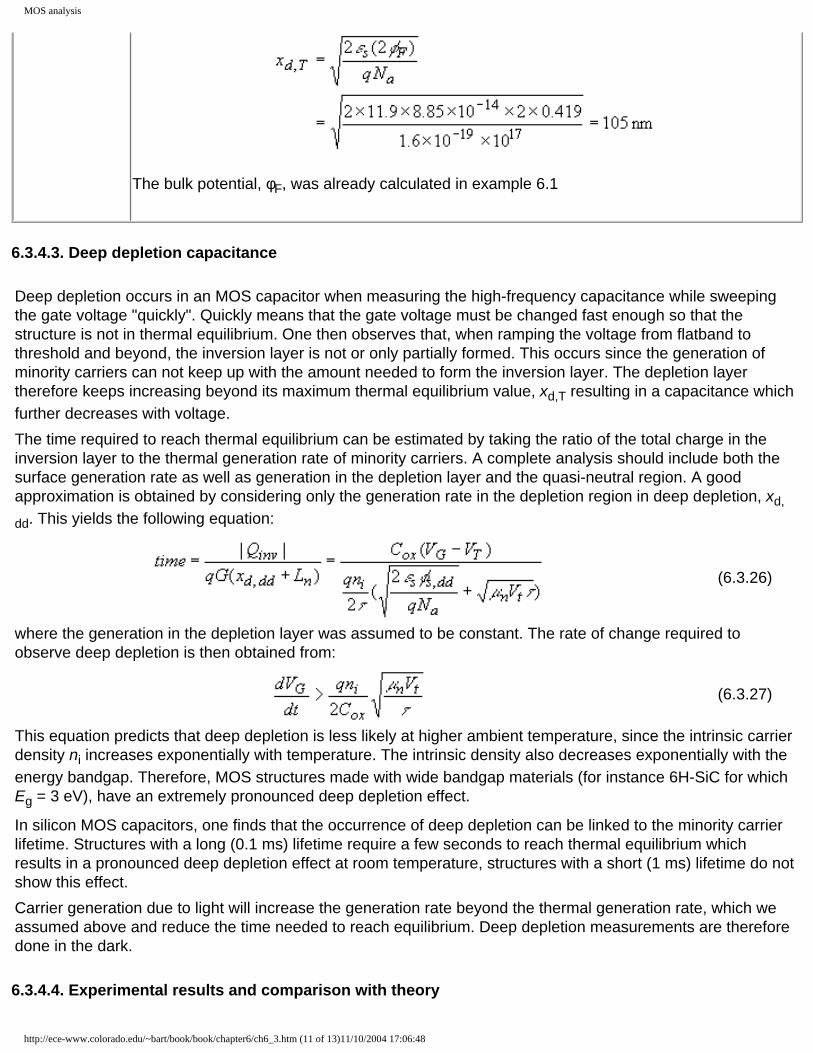
MOS analysis
The bulk potential, φF, was already calculated in example 6.1
6.3.4.3. Deep depletion capacitance
Deep depletion occurs in an MOS capacitor when measuring the high-frequency capacitance while sweeping the gate voltage "quickly". Quickly means that the gate voltage must be changed fast enough so that the structure is not in thermal equilibrium. One then observes that, when ramping the voltage from flatband to threshold and beyond, the inversion layer is not or only partially formed. This occurs since the generation of minority carriers can not keep up with the amount needed to form the inversion layer. The depletion layer therefore keeps increasing beyond its maximum thermal equilibrium value, xd,T resulting in a capacitance which further decreases with voltage. The time required to reach thermal equilibrium can be estimated by taking the ratio of the total charge in the inversion layer to the thermal generation rate of minority carriers. A complete analysis should include both the surface generation rate as well as generation in the depletion layer and the quasi-neutral region. A good approximation is obtained by considering only the generation rate in the depletion region in deep depletion, xd,
dd. This yields the following equation:
(6.3.26)
where the generation in the depletion layer was assumed to be constant. The rate of change required to observe deep depletion is then obtained from:
(6.3.27)
This equation predicts that deep depletion is less likely at higher ambient temperature, since the intrinsic carrier density ni increases exponentially with temperature. The intrinsic density also decreases exponentially with the energy bandgap. Therefore, MOS structures made with wide bandgap materials (for instance 6H-SiC for which Eg = 3 eV), have an extremely pronounced deep depletion effect.
In silicon MOS capacitors, one finds that the occurrence of deep depletion can be linked to the minority carrier lifetime. Structures with a long (0.1 ms) lifetime require a few seconds to reach thermal equilibrium which results in a pronounced deep depletion effect at room temperature, structures with a short (1 ms) lifetime do not show this effect. Carrier generation due to light will increase the generation rate beyond the thermal generation rate, which we assumed above and reduce the time needed to reach equilibrium. Deep depletion measurements are therefore done in the dark.
6.3.4.4. Experimental results and comparison with theory
http://ece-www.colorado.edu/~bart/book/book/chapter6/ch6_3.htm (11 of 13)11/10/2004 17:06:48

MOS analysis
As an example, we show below the measured low frequency (quasi-static) and high frequency capacitance-voltage curves of an MOS capacitor. The capacitance was measured in the presence of ambient light as well as in the dark as explained in Figure 6.3.5.
Figure 6.3.5 : Low frequency (quasi-static) and high frequency capacitance measurement of a pMOS capacitor. Shown are, from top to bottom, the low frequency capacitance measured in the presence of ambient light (top curve), the low frequency capacitance measured in the dark, the high frequency capacitance measured in the presence of ambient light and the high frequency capacitance measured in the dark (bottom curve). All curves were measured from left to right. The MOS parameters are Na - Nd = 4 x 1015 cm-3 and tox = 80 nm. The device area is 0.0007 cm2.
Figure 6.3.5 illustrates some of the issues when measuring the capacitance of an MOS capacitance. First, one should measure the devices in the dark. The presence of light causes carrier generation in the semiconductor, which affects the measured capacitance. In addition, one must avoid the deep depletion effects such as the initial linearly varying capacitance of the high frequency capacitance measured in the dark on the above figure (bottom curve). The larger the carrier lifetime, the slower the voltage is to be changed to avoid deep depletion. The low frequency measured is compared to the theoretical value in Figure 6.3.6. The high frequency capacitance measured in the presence of light is also shown on the figure. The figure illustrates the agreement between experiment and theory. A comparison of the experimental low (rather than high) frequency capacitance with theory is somewhat easier to carry out. The low frequency capacitance is easier to calculate while the measurement tends to be less sensitive to deep depletion effects.
http://ece-www.colorado.edu/~bart/book/book/chapter6/ch6_3.htm (12 of 13)11/10/2004 17:06:48
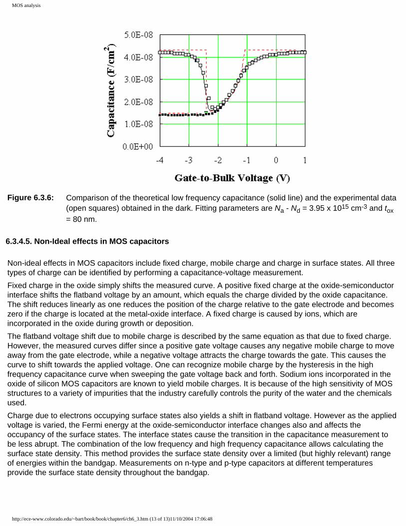
MOS analysis
Figure 6.3.6: Comparison of the theoretical low frequency capacitance (solid line) and the experimental data (open squares) obtained in the dark. Fitting parameters are Na - Nd = 3.95 x 1015 cm-3 and tox = 80 nm.
6.3.4.5. Non-Ideal effects in MOS capacitors
Non-ideal effects in MOS capacitors include fixed charge, mobile charge and charge in surface states. All three types of charge can be identified by performing a capacitance-voltage measurement. Fixed charge in the oxide simply shifts the measured curve. A positive fixed charge at the oxide-semiconductor interface shifts the flatband voltage by an amount, which equals the charge divided by the oxide capacitance. The shift reduces linearly as one reduces the position of the charge relative to the gate electrode and becomes zero if the charge is located at the metal-oxide interface. A fixed charge is caused by ions, which are incorporated in the oxide during growth or deposition. The flatband voltage shift due to mobile charge is described by the same equation as that due to fixed charge. However, the measured curves differ since a positive gate voltage causes any negative mobile charge to move away from the gate electrode, while a negative voltage attracts the charge towards the gate. This causes the curve to shift towards the applied voltage. One can recognize mobile charge by the hysteresis in the high frequency capacitance curve when sweeping the gate voltage back and forth. Sodium ions incorporated in the oxide of silicon MOS capacitors are known to yield mobile charges. It is because of the high sensitivity of MOS structures to a variety of impurities that the industry carefully controls the purity of the water and the chemicals used. Charge due to electrons occupying surface states also yields a shift in flatband voltage. However as the applied voltage is varied, the Fermi energy at the oxide-semiconductor interface changes also and affects the occupancy of the surface states. The interface states cause the transition in the capacitance measurement to be less abrupt. The combination of the low frequency and high frequency capacitance allows calculating the surface state density. This method provides the surface state density over a limited (but highly relevant) range of energies within the bandgap. Measurements on n-type and p-type capacitors at different temperatures provide the surface state density throughout the bandgap.
http://ece-www.colorado.edu/~bart/book/book/chapter6/ch6_3.htm (13 of 13)11/10/2004 17:06:48

MOS capacitor technology
Title Page Table of Contents Help Copyright B. Van Zeghbroeck, 2004
Chapter 6: MOS Capacitors
6.4. MOS capacitor technology
The fabrication of the oxide of an MOS structure is one of the critical steps when fabricating MOSFETs. This is in part due to the need for an ideal oxide-semiconductor interface with low surface-state density but also because of the extremely thin oxides that are currently used for sub-micron MOSFETs. Two techniques are commonly used to form silicon dioxide. One involves the oxidation of the silicon yielding a thermal oxide. The other technique relies on the deposition of SiO2 using a chemical vapor-deposition (CVD) process.
The thermal oxidation of silicon is obtained by heating the wafer in an oxygen or water vapor ambient. Typical temperatures range from 800 to 1200°C. The oxidation of a silicon surface also occurs at room temperature but the resulting 3 nm layer of oxide limits any further oxidation. At high temperatures, oxygen or water molecules can diffuse through the oxide so that further oxidation takes place. The oxidation in oxygen ambient is called a dry oxidation. The one in water vapor is a wet oxidation. The thermal oxidation provides a high quality interface and oxide. It is used less these days because of the high process temperatures.The deposition of SiO2 using a CDV process is one where two gases, silane and oxygen, react to form silicon dioxide, which then sublimes onto any solid surface. The wafers are heated to 200 - 400°C yielding high quality oxides. The lower process temperature and the quality of the deposited layers make CVD deposition the preferred method to fabricate MOS oxides.
http://ece-www.colorado.edu/~bart/book/book/chapter6/ch6_4.htm11/10/2004 17:07:03

MOS capacitor technology
Title Page Table of Contents Help Copyright B. Van Zeghbroeck, 2004
Chapter 6: MOS Capacitors
6.5. Exact MOS Analysis Note:This is a temporary file, which is to be replaced with a fully hyperlinked HTML file. Meanwhile, the text can be accessed by clicking on the PDF icon.
http://ece-www.colorado.edu/~bart/book/book/chapter6/ch6_5.htm11/10/2004 17:07:11

6.5. Exact MOS analysis
6.5.1. Introduction
An exact analytic solution can be obtained for the MOS capacitance as long as surface electron concentration is not degenerate. Poisson’s equation can then be solved yielding first the electric field as a function of the potential in the semiconductor. A solution for the electric field and/or the potential as a function of the position cannot be obtained analytically. This requires a numeric integration. Combining the electrical field and the surface potential yields the gate voltage, since the field in the semiconductor and that in the oxide are related by their respective dielectric constants. The same approach also yields a good approximation for the charge in the depletion layer, the inversion layer or the accumulation layer. The derivative of the charge with the applied voltage equals the capacitance of the MOS structure. The calculation of the low frequency or quasi-static capacitance is relative straight forward, while the calculation of the high-frequency capacitance requires an additional numeric integration. A detailed derivation of the items mentioned above as well as the deep depletion capacitance and an approximate expression for the high-frequency capacitance can be found in the full derivation.
6.5.2. Electric field versus surface potential
The solution for the electric field is obtained by solving Poisson's equation while including the charge due to electrons, holes and the ionized donors and acceptors. This solution provides the relation between the electric field at the surface of the semiconductor and the surface potential. The absolute value of the field is shown in the figure below. This figure was obtained for a substrate with an acceptor concentration, Na = 1017 cm-3, and an oxide thickness, tox = 20 nm.
Figure 6.5.1 Electric field at the surface of the semiconductor as a function of the potential across the semiconductor. Shown is the electric field (solid line) and the field due to the inversion layer charge only (black dotted line) The red vertical line indicates the threshold voltage. Na = 1017 cm-3 and tox = 20 nm.
When applying a positive potential (which can be done by applying a positive gate voltage) the surface of the silicon is first depleted. This causes an electric field, which varies as the square

root of the surface potential. At higher positive potential the surface inverts which results in a sharp rise of the electric field since the inversion layer charge increases exponentially with the surface potential. The vertical dotted line on the figure indicates the threshold voltage or the onset of strong inversion. The other dotted line represents the fraction of the surface field, which is due to the electrons in the inversion layer. It is calculated from the ratio of the inversion layer charge and the dielectric constant of the semiconductor.
When applying a negative surface potential, the holes accumulate at the surface, yielding an exponential rise of the electric field with decreasing potential.
An MOS structure with a n-type substrate can also be analyzed by entering a negative doping density.
6.5.3. Charge in the inversion layer
The total charge in the inversion layer can also be calculated with this method. It is obtained by subtracting the charge in the depletion layer from the total charge for the same surface potential. The details can be found in the full derivation. The gate voltage is obtained by adding the flat band voltage, the surface potential and the voltage across the oxide. The resulting charge density is plotted versus the gate voltage in the figure below. This figure was calculated for an oxide thickness of 20 nm. The doping density is also 1017 cm-3 as before.
Figure 6.5.2 Charge density due to electrons in the inversion layer of an MOS capacitor. Compared are the analytic solution (solid line) and our basic assumption (dotted line). Na = 1017 cm-3 and tox = 20 nm.
The dotted line on the figure represents the standard approximation for the inversion layer charge: it implies that the charge is simply proportional to the gate oxide capacitance and the gate voltage minus the threshold voltage. For voltages below the threshold voltage, there is no inversion layer and therefore no inversion layer charge. While not exact, the standard approximation is very good.

6.5.4. Low frequency capacitance
The low frequency or quasi-static capacitance can be obtained by taking the derivative of the charge in the semiconductor with respect to the potential across the semiconductor. Since this derivative represents the change between two thermal equilibrium situations, this capacitance is also to be measured while maintaining equilibrium conditions at all times. The low frequency or quasi-static measurement is typically obtained by measuring the current with a sensitive electrometer while varying the applied gate voltage.
The expected behavior of such measurement is shown in the figure below: The capacitance is close to the oxide capacitance except for a gate voltage between the flat band voltage and the threshold voltage, as charge is then added deeper into the semiconductor at the edge of the depletion layer, rather than at the oxide-silicon interface. This results in the characteristic dip in the capacitance curve.
Figure 6.5.3 Low frequency capacitance of an MOS capacitor. Shown is the exact solution for the low frequency capacitance (solid line) and the low and high frequency capacitance obtained with the simple model (dotted lines). The red square indicates the flatband voltage and capacitance, while the green square indicates the threshold voltage and capacitance. Na = 1017 cm-3 and tox = 20 nm.
This figure was calculated using an oxide thickness of 20 nm and an acceptor concentration of 1017 cm-3. The dotted lines indicate the high- and low-frequency capacitance as obtained using the full depletion approximation. It is clear from the figure that the approximation is rather crude when it comes to describing the full behavior, but it is sufficient to extract the oxide thickness and substrate doping concentration from a measured curve.

6.5.5. Derivation of the exact solution
We now derive the exact solution of the MOS capacitor. Whereas most of the derivation is applicable for n-type and p-type substrates, the equations are written in a form, which is more convenient for p-type substrates, but can be rewritten for n-type substrates.
The total charge density, ρ, in the semiconductor is given by:
)( −+ −−+= ad NnNpqρ (6.5.1)
Under thermal equilibrium, the hole and electron densities, p and n, can be expressed as a function of the potential, φ, and a reference potential, φF.
)
)(exp(
t
Fi V
xnp
φφ −=
(6.5.2)
)
)(exp(
t
Fi V
xnn
φφ −=
(6.5.3)
far away from the oxide-semiconductor interface, the charge density is zero and we define the potential, φ, to be zero there also, so that
)sinh(2
t
Fiad V
nNNφ
−=− −+ (6.5.4)
Poisson's equation then takes the following form:
)sinh()sinh(
22
2
t
F
t
F
s
iVV
qn
dx
d φφφε
φ+
−=
(6.5.5)
multiplying both sides of the equation with 2 dφ/dx and integrating while replacing -dφ/dx by the electric field E, one obtains:
)sinh()cosh(
4)(sign)( K
VVVVqn
t
F
tt
F
s
ti ++−
=φφφφ
εφφE
(6.5.6)
the constant K can be determined from the boundary condition at x = ∞ where φ = E = 0 yielding
)cosh(
t
FV
Kφ
−= (6.5.7)
The electric field has the same sign as the potential as described with the sign function.
The relation between the field and the potential at the surface under thermal equilibrium is then:

)cosh()sinh()cosh()(sign 2,
t
F
t
F
t
s
t
Fs
s
tiseqs VVVV
Vqn φφφφφε
φ −+−
=E
(6.5.8)
The gate voltage can be expressed as a function of the flatband voltage, the voltage across the oxide and the potential across the semiconductor:
oxsFBG VVV ++= φ , with
ox
sseqsoxox tV
εε
φ )(,E= (6.5.9)
6.5.5.1.Low frequency capacitance
The low frequency capacitance of the MOS structure per unit area can then be calculated from:
LFsoxox
sseqsoxs
eqss
G
sLF
CCtd
d
dVdQ
C
,,
,
111
))(( +=
+==
εε
φφε
E
E
(6.5.10)
where Cox = εox/tox and
)cosh()sinh()cosh(
)sinh()sinh(
,,
t
F
t
F
t
s
t
Fs
t
F
t
Fs
ts
is
s
eqssLFs
VVVV
VVV
qn
dd
C
φφφφφ
φφφ
εε
φε
−+−
+−
=
=E
(6.5.11)
)]sinh()[sinh(2
,,
t
F
t
Fs
eqs
iLFs VV
qnC
φφφ+
−=
E
(6.5.12)
This result is often referred to as the low frequency capacitance of a MOS capacitor since we calculated the change in charge between two equilibrium situations. The result can be interpreted as a series connection of the oxide capacitance and the low frequency capacitance of the semiconductor Cs,LF. By starting from a series of values for φs, one can use the above equations to first calculate the electric field, the gate voltage and the capacitance. This enables to plot the low frequency capacitance as a function of the gate voltage as shown in Figure 6.5.4.

VG [VOLT]
C/C
ox
0
0.2
0.4
0.6
0.8
1
-3 -2 -1 0 1 2 3
Figure 6.5.4 Capacitance versus voltage for a MOS structure with Na = 1015 cm-3 and tox = 0.1 µm. The curves from top to bottom are: The low frequency capacitance, the approximate high frequency capacitance, the exact high frequency capacitance and the capacitance under deep depletion conditions. The dotted line indicates Cmin, the capacitance at the onset of strong inversion calculated using the full depletion approximation.
Under flat-band conditions, where 0 = |φs| < Vt, the capacitance reduces to
s
D
ox
FB LC
C
ε+
=1
1
(6.5.13)
where LD is the extrinsic Debye length in the semiconductor with doping |Na - Nd|:
da
tsD NNq
VL
−=
ε
(6.5.14)
6.5.5.2.Deep depletion capacitance
If the gate voltage is changed faster than electrons can be generated at the oxide-semiconductor interface to obtain the equilibrium density, no inversion layer is generated. In this case the gate voltage will cause the depletion layer in the semiconductor to exceed the maximum depletion layer width as defined at the onset of strong inversion. A typical measurement starts from an

equilibrium situation where no inversion layer is present and the gate voltage is swept rapidly while creating a depletion layer in the semiconductor. The capacitance is measured as the change in charge flowing into the structure for a given voltage change. For a p-type substrate, this situation can be modeled by eliminating the charge term due to electrons in Poisson's equation:
)exp()sinh(2
2
2
t
F
t
F
s
i
VVqn
dxd φφφ
εφ −
−= (6.5.15)
Using the same procedure as above the relation between surface field and surface potential can be found:
)1))(exp(exp()sinh(2
2)(sign, −
−+=
t
s
t
F
t
F
t
s
s
tisdds VVVV
Vqn φφφφε
φE (6.5.16)
and the capacitance of the semiconductor becomes:
)]exp()sinh(2[
,,
t
sF
t
F
dds
idds VV
qnC
φφφ −−=
E
(6.5.17)
and the corresponding gate voltage is:
oxsFBG VVV ++= φ , with
ox
ssddsoxox tV
εε
φ )(,E= (6.5.18)
Using a similar procedure as for the low frequency capacitance we can also plot the capacitance under deep depletion conditions.
6.5.5.3.High frequency capacitance
The high frequency capacitance of an MOS capacitor is measured by applying a small ac voltage in addition to the DC gate voltage. The capacitance is defined as the ratio of the out-of-phase component of the ac current divided by the amplitude of the ac voltage times the radial frequency. An approximate expression can be obtained by ignoring the change in charge in the inversion layer yielding the expression for the capacitance under deep depletion conditions. However since the gate voltage is changed slowly while measuring the capacitance versus voltage, the gate voltage is calculated from the surface potential including the charge in the inversion layer under thermal equilibrium. The capacitance is then given by:
)]exp()sinh(2[
,,
t
sF
t
F
dds
iHFs VV
qnC
φφφ −−=
E
(6.5.19)
with the electric field, Es,dd, obtained under deep depletion conditions (6.5.16).
This is the same expression as for the capacitance under deep depletion conditions. However, the corresponding gate voltage is different, namely:
oxsFBG VVV ++= φ , with
ox
sseqsoxox tV
εε
φ )(,E= (6.5.20)

where the electric field, Es,eq, is the thermal equilibrium field
The corresponding capacitance is also included in Figure 6.5.4 together with the expected minimum capacitance based on the full depletion approximation corrected for the thermal voltage:
sa
tF
ox qNV
CC εφ )2(211
min
++=
(6.5.21)
It should be stressed that this is only an approximate solution. The redistribution of the inversion layer charge with applied gate voltage is ignored in the approximate solution even though it does affect the depletion layer width and with it the capacitance. This approximation therefore introduces an error which was found to be less than 6% at the onset of strong inversion and which increases almost linearly with increasing surface potential.
The exact expression for the high frequency capacitance1 used in Figure 6.5.4 is:
∆+−
−+−−×
=
1]1)[exp(
)exp()]exp(1)[exp(
)(
,,,
sFsF
eqs
siexactHFs
UUUU
signqnC
Eφ
(6.5.22)
Where ∆ for a p-type substrate is:
0=∆ for φs < 0 and φF > 0 (6.5.23)
∫−−−−−
−−
=∆sU
F
F
Fs
ss
dUF
U
UUFUU
03 )|(2
)1)))(exp(exp(1)(exp(
)|()1)(exp(
ξξ
ξξξ for φs > 0 and φF > 0
(6.5.24)
The expression with ∆ = 0 for all possible surface potentials equals the low frequency capacitance. The function F is related to the equilibrium electric field by:
t
iDeqF
V
LUUF
22)|( ,E
= (6.5.25)
and the normalized parameters U, Us and UF are defined as:
U = φ/Vt, Us = φs/Vt,UF = φF/Vt (6.5.26)
Where the gate voltage is still given by:
1A derivation of this expression can be found in "MOS (Metal Oxide Semiconductor) Physics and Technology", E. H. Nicollian and J. R. Brews, Wiley and Sons, 1982, p 157.

oxsFBG VVV ++= φ , with
ox
sseqsoxox tV
εε
φ )(,E= (6.5.27)
and the electric field, Es,eq, is the thermal equilibrium field at the surface.
As illustrated with Fig.A6.2, the high frequency capacitance at the onset of strong inversion (φs=2φF) and beyond is found to be almost constant. Assuming φF >> Vt one finds
F
saHFs
qNC
φε
4, = , for ox
FsaFFBG C
qNVV
φεφ
42 +>−
(6.5.28)
this result could also be obtained by calculating the depletion region width in the semiconductor assuming the maximum potential at the surface to be 2φF and using the full depletion approximation. The low frequency capacitance at φs = 2φF, assuming φF >> Vt is then:
F
saLFs
qNC
φε2
, = , for ox
FsaFFBG C
qNVV
φεφ
42 +=−
(6.5.29)
also yielding the following relation between both:
HFsLFs CC ,, 8= , for Fs φφ 2= (6.5.30)

MOS capacitor technology
Title Page Table of Contents Help Copyright B. Van Zeghbroeck, 2004
Chapter 6: MOS Capacitors
6.6. pMOS equations Note:This is a temporary file, which is to be replaced with a fully hyperlinked HTML file. Meanwhile, the text can be accessed by clicking on the PDF icon.
http://ece-www.colorado.edu/~bart/book/book/chapter6/ch6_6.htm11/10/2004 17:09:15

6.6. p-MOS and general equations
6.6.1. p-MOS equations
p-MOS capacitors have an n-type substrate, a positive charge in the depletion layer and a positive charge in the inversion layer. Since the Fermi energy is a distance qφF above the midgap energy level, the work function difference is given by:
)
2( F
gMSMMS q
Eφχ −+−Φ=Φ−Φ=Φ , n-substrate
(6.6.1)
with
i
dtF n
NV ln=φ , n-substrate
(6.6.2)
The expression for the depletion layer width is similar to that of n-MOS capacitors, namely:
d
FsTd qN
xφε 22
, = , n-substrate (6.6.3)
while the threshold is typically negative due to the positive charge in the depletion layer width.
ox
dFsFFBT C
qNVV
φεφ
222 −−= , n-substrate
(6.6.4)
Note that the relation between the flatband voltage and the workfunction difference still applies:
∫−−Φ=oxt
oxoxox
iMSFB dxxx
CQ
V0
)(1
ρε
, n-substrate (6.6.5)
6.6.2. General equations
General equations, which are valid for n-MOS and p-MOS capacitors are provided below. The type is directly linked to the net doping density of the substrate, Na - Nd, which is positive for a p-type substrate (n-MOS capacitor) and negative for an n-type substrate (p-MOS capacitor). The workfunction difference is then given by:
)
2( F
icMSMMS q
EEφχ +
−+−Φ=Φ−Φ=Φ , n-substrate
(6.6.6)
where the built-in potential is positive for p-type substrates and negative for n-type substrates and is given by:
it
itF n
nV
np
V lnln −==φ , n-substrate (6.6.7)

The depletion layer width at threshold is then:
)(22
,da
FsTd NNq
x−
=φε
(6.6.8)
and the threshold voltage is given by:
(6.6.9)
These equations are of interest when parameters of n-MOS as well as p-MOS capacitors are to be calculated. The equations eliminate the problem of the variable signs and possible mistakes and confusion, at the expense of the added complexity. These equations have been implemented in the active figures.
In a MOSFET structure it is possible to apply a voltage to the channel, VC relative to the voltage at the bulk contact to the substrate, VB. This affects the width of the depletion layer width at threshold:
)()2(2
,da
BCFsTd NNq
VVx
−−+
=φε
(6.6.10)
as well as the threshold voltage itself:
)()2(2)(
2da
BCFs
ox
daFCFBT NNq
VVC
NNqVVV
−−+−
+++=φε
φ (6.6.11)
This expression will be needed to derive the variable depletion layer model of the MOSFET.

MOS capacitor technology
Title Page Table of Contents Help Copyright B. Van Zeghbroeck, 2004
Chapter 6: MOS Capacitors
6.7. Charge Coupled Devices Note:This is a temporary file, which is to be replaced with a fully hyperlinked HTML file. Meanwhile, the text can be accessed by clicking on the PDF icon.
http://ece-www.colorado.edu/~bart/book/book/chapter6/ch6_7.htm11/10/2004 17:09:38

6.7. Charge coupled devices Application of MOS capacitors
Serial memory – delay line – analog signal processor – camera focal plane array
6.7.1. Structure and principle of operation
Charge coupled devices (CCDs) consist of a series of closely spaced MOS capacitors
Capacitors operate in deep depletion
3-phase clock
1 bit per 3 capacitors
charge moves to lowest
Diffusion time is given by
nd D
L2
24π
τ = (6.7.1)
Example:
Consider a silicon CCD array with 5 µm wide electrodes. Calculate the diffusion time. Use an electron mobility of 400 cm2/V-s.
Solution
The diffusion time equals
nd D
L2
24π
τ = =10 ns
6.7.2. Buried channel CCD/improvements/variations
6.7.2.1.Buried channel CCD
Contain an n-type layer typically added by ion implantation.
Intention is to separate the charge from the substrate for higher mobility and minority carrier lifetime. Smith and Boyle
6.7.2.2.Overlapping electrodes
6.7.3. CCD cameras
Combination of detectors with CCD readout
Color filters to get color image

6.7.4. Derivation of the diffusion time
Diffusion time is given by
nd D
L2
24π
τ = (6.7.2)
Derivation starts from the time dependent continuity equation
),(),(
),(1),(txRtxG
xtxJ
qttxn
nnn −+∂
∂=
∂∂
(6.7.3)
Simplify by eliminating any generation or recombination and diffusion only, resulting in the time dependent diffusion equation:
2
2 ),(),(x
txnD
ttxn
n ∂∂
=∂
∂
(6.7.4)
A general solution to this partial differential equation can be obtained by assuming that the carrier density can be written as the product of a function T(t), which only depends on time and a function X(x), which only depends on position. Substitution into the diffusion equation and rearrangment resuots in two parts, one a function of t only and one a function of x only. Since both have to equal each other they must equal a constant. The unit of the constant is s-1 and one would expect the desired solution to decrease with time so that the equation can be rewritten as:
dn x
tXtT
DttT
tT τ1)(
)(1)(
)(1
2
2
−=∂
∂=
∂∂
(6.7.5)
The general solution is therefore
)sincos)(exp(),(
dndnd Dx
BDx
At
txnτττ
+−= (6.7.6)
Where the constants A and B must be determined. At x = 0, there is no current since the potential barrier caused by the lower voltage applied to the electrode to the left block any carrier flow. Since the diffusion current depends on the gradient of the current, the derivative of the carrier density must be zero, which eliminates the sine function as a possible solution. The solution therefore reduces to:
dnd Dxt
ntxnττ
cos)exp()0,0(),( −= (6.7.7)
Where n(0,0) is the initial carrier density at x = t = 0
The boundary condition at x = L is obtained by assuming that the electric field between two adjacent capacitors will immediately remove any carriers that arrive so that the carrier density is zero at any time, t, so that n(L,t) = 0. The argument of the cosine function should therefore equal

π/2. From this one then finds the diffusion time constant, τd.
nd D
L2
24π
τ = (6.7.8)

example 3
Title Page Table of Contents Help Copyright B. Van Zeghbroeck, 2004
Chapter 6: MOS Capacitors
Examples
Example 6.1 Calculate the flatband voltage of a silicon nMOS capacitor with a substrate doping Na = 1017 cm-3 and an aluminum gate (ΦM = 4.1 V). Assume there is no fixed charge in the oxide or at the oxide-silicon interface.
Example 6.2 Calculate the threshold voltage of a silicon nMOS capacitor with a substrate doping Na = 1017 cm-3, a 20 nm thick oxide (εox = 3.9 ε0) and an aluminum gate (ΦM = 4.1 V). Assume there is no fixed charge in the oxide or at the oxide-silicon interface.
Example 6.3 Calculate the oxide capacitance, the flatband capacitance and the high frequency capacitance in inversion of a silicon nMOS capacitor with a substrate doping Na = 1017 cm-
3, a 20 nm thick oxide (εox = 3.9 ε0) and an aluminum gate (ΦM = 4.1 V).
http://ece-www.colorado.edu/~bart/book/book/chapter6/ch6_ex.htm11/10/2004 17:09:56

Example 6.1 Calculate the flatband voltage of a silicon nMOS capacitor with a substrate doping Na = 1017 cm-3 and an aluminum gate (ΦM = 4.1 V). Assume there is no fixed charge in the oxide or at the oxide-silicon interface.
Solution The flatband voltage equals the work function difference since there is no charge in the oxide or at the oxide-semiconductor interface.
V 93.010
10ln026.056.005.41.4
ln2
10
17−=×−−−=
−−−Φ=Φ=i
at
gMMSFB n
NV
q
EV χ
The flatband voltages for nMOS and pMOS capacitors with an aluminum or a poly-silicon gate are listed in the table below. Aluminum p+ poly n+ poly nMOS -0.93 V 0.14 V -0.98 V
pMOS -0.09 V 0.98 V -0.14 V

Example 6.2 Calculate the threshold voltage of a silicon nMOS capacitor with a substrate doping Na = 1017 cm-3, a 20 nm thick oxide (εox = 3.9 ε0) and an aluminum gate (ΦM = 4.1 V). Assume there is no fixed charge in the oxide or at the oxide-silicon interface.
Solution The threshold voltage equals:
V 09.0 1020/1085.89.3
42.010106.11085.89.114
42.0293.0
42
714
171914
−=×××
×××××××+
×+−=
++=
−−
−−
ox
FasFFBT C
qNVV
φεφ
Where the flatband voltage was already calculated in example 6.1. The threshold voltage voltages for nMOS and pMOS capacitors with an aluminum or a poly-silicon gate are listed in the table below. Aluminum p+ poly n+ poly nMOS -0.09 V 0.98 V -0.14 V
pMOS -0.93 V 0.14 V -0.98 V
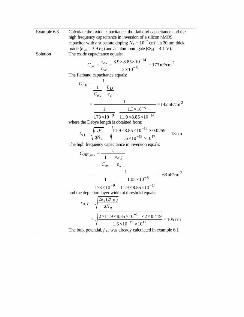
Example 6.3 Calculate the oxide capacitance, the flatband capacitance and the high frequency capacitance in inversion of a silicon nMOS capacitor with a substrate doping Na = 1017 cm-3, a 20 nm thick oxide (εox = 3.9 ε0) and an aluminum gate (ΦM = 4.1 V).
Solution The oxide capacitance equals:
26
14nF/cm 173
102
1085.89.3=
×
××==
−
−
ox
oxox t
Cε
The flatband capacitance equals:
2
14
6
9
nF/cm 142
1085.89.11
103.1
10173
1
1
11
=
××
×+
×
=
+=
−
−
−
s
D
ox
FB LC
C
ε
where the Debye length is obtained from:
nm 1310106.1
0259.01085.89.111719
14=
××
×××==
−
−
a
tsD qN
VL
ε
The high frequency capacitance in inversion equals:
2
14
5
9
,,
nF/cm 63
1085.89.11
1005.1
10173
1
1
11
=
××
×+
×
=
+=
−
−
−
s
Td
ox
invHF x
C
C
ε
and the depletion layer width at threshold equals:
nm 10510106.1
419.021085.89.112
)2(2
1719
14
,
=××
×××××=
=
−
−
a
FsTd Nq
xφε
The bulk potential, φF, was already calculated in example 6.1
http://ece-www.colorado.edu/~bart/book/book/chapter6/ch6_p.htm
Title Page Table of Contents Help Copyright B. Van Zeghbroeck, 2004
Chapter 6: MOS Capacitors
Problems
1. Consider an aluminum-SiO2-silicon MOS capacitor (ΦM = 4.1 V, εox/ε0 = 3.9, χ = 4.05 V and Na = 1017 cm-3) MOS capacitor with tox = 5 nm.
a. Calculate the flatband voltage and threshold voltage. b.
Repeat for an n-type silicon substrate with Nd= 1016cm-3. c.
Repeat with a surface charge of 10-7C/cm2
d. Repeat with a charge density in the oxide of 10-1C/cm3
A high-frequency capacitance voltage measurement of a silicon MOS structure was fitted by the following expression:
C(VG) = 6 pF + 12 pF/(1 + exp(VG))
a. Calculate the oxide capacitance per unit area and the oxide thickness. The area of the capacitor is 100 x 100 micron and the relative dielectric constant equals 3.9.
From the minimum capacitance, calculate the maximum depletion layer width and the substrate doping density. Calculate the bulk potential. Calculate the flatband capacitance and the flatband voltage. Calculate the threshold voltage.
An MOS capacitor with an oxide thickness of 20 nm has an oxide capacitance, which is three times larger than the minimum high-frequency capacitance in inversion. Find the substrate doping density.
A CMOS gate requires n-type and p-type MOS capacitors with a threshold voltage of 2 and -2 Volt respectively. If the gate oxide is 50 nm what are the required substrate doping densities? Assume the gate electrode is aluminum. Repeat for a p+ poly-silicon gate.
Consider a p-MOS capacitor (with an n-type substrate) and with an aluminum gate. Find the doping density for which the threshold voltage is 3 times larger than the flat band voltage. tox = 25 nm. Repeat for a capacitor with 1011 cm-2 electronic charges at the oxide-semiconductor interface.
A silicon p-MOS capacitor . (Nd = 4 x 1016 cm-3, tox = 40 nm) is biased halfway between the flatband and threshold voltage. Calculate the applied voltage and the corresponding capacitance
http://ece-www.colorado.edu/~bart/book/book/chapter6/ch6_p.htm11/10/2004 17:10:16

Chapter 6 Review questions
Title Page Table of Contents Help Copyright B. Van Zeghbroeck, 2004
Chapter 6: MOS Capacitors
Review Questions
1. Draw an MOS flatband diagram. Indicate the workfunction of the metal and the semiconductor as well as the flatband voltage. Draw it approximately to scale using ΦM = 4.1 V, χ = 4.05 V, Eg = 1.12 eV (silicon) and Na = 1016 cm-3.
2. Derive the metal-semiconductor workfunction for n-type and p-type poly-silicon gate structures. (equation 6.3.2)
3. Explain why the flatband voltage depends on the charge in the oxide or at the oxide-semiconductor interface.
4. Name the three bias regimes of an MOS capacitor and explain what happens in the semiconductor in each of these bias modes.
5. What is the basic assumption regarding the charge in the inversion layer?
6. What are the assumptions of the MOS capacitor analysis?
7. What is the difference between the high frequency and quasi-static capacitance?
8. Why is the high frequency capacitance constant in inversion?
9. Why does the flatband capacitance not equal the oxide capacitance?
10. What is deep depletion?
11. Why does light illumination affect the capacitance of an MOS structure?
12. Name the non-ideal effects in MOS capacitors. What causes them and how do they affect the MOS characteristics?
http://ece-www.colorado.edu/~bart/book/book/chapter6/ch6_r.htm11/10/2004 17:10:25

http://ece-www.colorado.edu/~bart/book/book/chapter6/ch6_b.htm
Title Page Table of Contents Help Copyright B. Van Zeghbroeck, 2004
Chapter 6: MOS Capacitors
Bibliography
1. E. H. Nicollian and J. R. Brews, "MOS (Metal Oxide Semiconductor) Physics and Technology", John Wiley & Sons, 1982.
2. R. F. Pierret, "Field Effect Devices”, Second Edition, Addison-Wesley, 1990.
3. H. C. Casey, jr., "Devices For Integrated Circuits", John Wiley & Sons, 1999.
4. B. G. Streetman and S. Banerjee, "Solid State Electronic Devices", Fifth Edition, Prentice Hall, 2000.
http://ece-www.colorado.edu/~bart/book/book/chapter6/ch6_b.htm11/10/2004 17:10:34

Chapter 6 Equations
Title Page Table of Contents Help Copyright B. Van Zeghbroeck, 2004
Chapter 6: MOS Capacitors
Equations
(6.3.1)
(6.3.2)
(6.3.3)
(6.3.4)
(6.3.5)
(6.3.6)
(6.3.7)
(6.3.8)
http://ece-www.colorado.edu/~bart/book/book/chapter6/ch6_eq.htm (1 of 3)11/10/2004 17:10:42

Chapter 6 Equations
(6.3.9)
(6.3.10)
(6.3.11)
(6.3.12)
(6.3.13)
(6.3.14)
(6.3.15)
(6.3.16)
(6.3.17)
(6.3.18)
http://ece-www.colorado.edu/~bart/book/book/chapter6/ch6_eq.htm (2 of 3)11/10/2004 17:10:42

Chapter 6 Equations
(6.3.19)
(6.3.20)
(6.3.21)
(6.3.22)
(6.3.23)
(6.3.24)
(6.3.25)
(6.3.26)
(6.3.27)
http://ece-www.colorado.edu/~bart/book/book/chapter6/ch6_eq.htm (3 of 3)11/10/2004 17:10:42

MOS Field-Effect-Transistors
Title Page Table of Contents Help Copyright B. Van Zeghbroeck, 2004
Chapter 7: MOS Field-Effect-Transistors
7.1. Introduction
The n-type Metal-Oxide-Semiconductor Field-Effect-Transistor (nMOSFET) consists of a source and a drain, two highly conducting n-type semiconductor regions, which are isolated from the p-type substrate by reversed-biased p-n diodes. A metal or poly-crystalline gate covers the region between source and drain. The gate is separated from the semiconductor by the gate oxide. The basic structure of an n-type MOSFET and the corresponding circuit symbol are shown in Figure 7.1.1.
Figure 7.1.1 : Cross-section and circuit symbol of an n-type Metal-Oxide-Semiconductor-Field-Effect-Transistor (MOSFET)
As can be seen on the figure the source and drain regions are identical. It is the applied voltages, which determine which n-type region provides the electrons and becomes the source, while the other n-type region collects the electrons and becomes the drain. The voltages applied to the drain and gate electrode as well as to the substrate by means of a back contact are referred to the source potential, as also indicated Figure 7.1.1.
A conceptually similar structure was proposed and patented independently by Lilienfeld and Heil in 1930, but was not successfully demonstrated until 1960. The main technological problem was the control and reduction of the surface states at the interface between the oxide and the semiconductor. Initially it was only possible to deplete an existing n-type channel by applying a negative voltage to the gate. Such devices have a conducting channel between source and drain even when no gate voltage is applied and are called "depletion-mode" devices.A reduction of the surface states enabled the fabrication of devices, which do not have a conducting channel unless a positive voltage is applied. Such devices are referred to as "enhancement-mode" devices. The electrons at the oxide-semiconductor interface are concentrated in a thin (~10 nm thick) "inversion" layer. By now, most MOSFETs are "enhancement-mode" devices.
http://ece-www.colorado.edu/~bart/book/book/chapter7/ch7_1.htm (1 of 2)11/10/2004 17:10:53

MOS Field-Effect-Transistors
While a minimum requirement for amplification of electrical signals is power gain, one finds that a device with both voltage and current gain is a highly desirable circuit element. The MOSFET provides current and voltage gain yielding an output current into an external load which exceeds the input current and an output voltage across that external load which exceeds the input voltage.The current gain capability of a Field-Effect-Transistor (FET) is easily explained by the fact that no gate current is required to maintain the inversion layer and the resulting current between drain and source. The device has therefore an infinite current gain in DC. The current gain is inversely proportional to the signal frequency, reaching unity current gain at the transit frequency.The voltage gain of the MOSFET is caused by the current saturation at higher drain-source voltages, so that a small drain-current variation can cause a large drain voltage variation.
http://ece-www.colorado.edu/~bart/book/book/chapter7/ch7_1.htm (2 of 2)11/10/2004 17:10:53
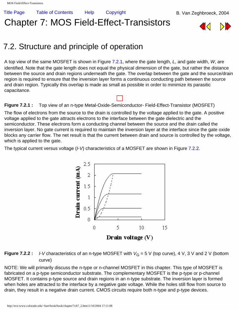
MOS Field-Effect-Transistors
Title Page Table of Contents Help Copyright B. Van Zeghbroeck, 2004
Chapter 7: MOS Field-Effect-Transistors
7.2. Structure and principle of operation
A top view of the same MOSFET is shown in Figure 7.2.1, where the gate length, L, and gate width, W, are identified. Note that the gate length does not equal the physical dimension of the gate, but rather the distance between the source and drain regions underneath the gate. The overlap between the gate and the source/drain region is required to ensure that the inversion layer forms a continuous conducting path between the source and drain region. Typically this overlap is made as small as possible in order to minimize its parasitic capacitance.
Figure 7.2.1 : Top view of an n-type Metal-Oxide-Semiconductor- Field-Effect-Transistor (MOSFET)The flow of electrons from the source to the drain is controlled by the voltage applied to the gate. A positive voltage applied to the gate attracts electrons to the interface between the gate dielectric and the semiconductor. These electrons form a conducting channel between the source and the drain called the inversion layer. No gate current is required to maintain the inversion layer at the interface since the gate oxide blocks any carrier flow. The net result is that the current between drain and source is controlled by the voltage, which is applied to the gate.The typical current versus voltage (I-V) characteristics of a MOSFET are shown in Figure 7.2.2.
Figure 7.2.2 : I-V characteristics of an n-type MOSFET with VG = 5 V (top curve), 4 V, 3 V and 2 V (bottom curve)
NOTE: We will primarily discuss the n-type or n-channel MOSFET in this chapter. This type of MOSFET is fabricated on a p-type semiconductor substrate. The complementary MOSFET is the p-type or p-channel MOSFET. It contains p-type source and drain regions in an n-type substrate. The inversion layer is formed when holes are attracted to the interface by a negative gate voltage. While the holes still flow from source to drain, they result in a negative drain current. CMOS circuits require both n-type and p-type devices.
http://ece-www.colorado.edu/~bart/book/book/chapter7/ch7_2.htm11/10/2004 17:11:08

MOSFET analysis
Title Page Table of Contents Help Copyright B. Van Zeghbroeck, 2004
Chapter 7: MOS Field-Effect-Transistors
7.3. MOSFET analysis7.3.1. The linear model7.3.2. The quadratic model7.3.3. The variable depletion layer model
In this section, we present three different models for the MOSFET, the linear model, the quadratic model and the variable depletion layer model. The linear model correctly predicts the MOSFET behavior for small drain-source voltages, where the MOSFET acts as a variable resistor. The quadratic model includes the voltage variation along the channel between source and drain. This model is most commonly used despite the fact that the variation of the depletion layer charge is ignored. The variable depletion layer model is more complex as it does include the variation of the depletion layer along the channel.
7.3.1. The linear model
The linear model describes the behavior of a MOSFET biased with a small drain-to-source voltage. As the name suggests, the MOSFET, as described by the linear model, acts as a linear device, more specifically a linear resistor whose resistance can be modulated by changing the gate-to-source voltage. In this regime, the MOSFET can be used as a switch for analog signals or as an analog multiplier. The general expression for the drain current equals the total charge in the inversion layer divided by the time the carriers need to flow from the source to the drain:
(7.3.1)
where Qinv is the inversion layer charge per unit area, W is the gate width, L is the gate length and tr is the transit time. If the velocity of the carriers is constant between source and drain, the transit time equals:
(7.3.2)
where the velocity, v, equals the product of the mobility and the electric field:
(7.3.3)
The constant velocity also implies a constant electric field so that the field equals the drain-source voltage divided by the gate length. This leads to the following expression for the drain current:
(7.3.4)
http://ece-www.colorado.edu/~bart/book/book/chapter7/ch7_3.htm (1 of 8)11/10/2004 17:11:19

MOSFET analysis
We now assume that the charge density in the inversion layer is constant between source and drain. We also assume that the basic assumption described in section 6.3.2 applies, namely that the charge density in the inversion layer is given by the product of the capacitance per unit area and the gate-to-source voltage minus the threshold voltage:
(7.3.5)
The inversion layer charge is zero if the gate voltage is lower than the threshold voltage. Replacing the inversion layer charge density in the expression for the drain current yields the linear model:
(7.3.6)
Note that the capacitance in the above equations is the gate oxide capacitance per unit area. Also note that the drain current is zero if the gate-to-source voltage is less than the threshold voltage. The linear model is only valid if the drain-to-source voltage is much smaller than the gate-to-source voltage minus the threshold voltage. This insures that the velocity, the electric field and the inversion layer charge density is indeed constant between the source and the drain.
Figure 7.3.1 : Linear I-V characteristics of a MOSFET with VT = 1 V. (µn = 300 cm2/V-s, W/L = 5 and tox = 20 nm).
The figure illustrates the behavior of the device in the linear regime: While there is no drain current if the gate voltage is less than the threshold voltage, the current increases with gate voltage once it is larger than the threshold voltage. The slope of the curves equals the conductance of the device, which increases linearly with the applied gate voltage. The figure clearly illustrates the use of a MOSFET as a voltage-controlled resistor.
7.3.2. The quadratic model
The quadratic model uses the same assumptions as the linear model except that the inversion layer charge density is allowed to vary in the channel between the source and the drain. The derivation is based on the fact that the current at each point in the channel is constant. The current can also be related to the local channel voltage.
http://ece-www.colorado.edu/~bart/book/book/chapter7/ch7_3.htm (2 of 8)11/10/2004 17:11:19

MOSFET analysis
Considering a small section within the device with width dy and channel voltage VC + VS one can still use the linear model described by equation (7.3.6), yielding:
(7.3.7)
where the drain-source voltage is replaced by the change in channel voltage over a distance dy, namely dVC. Both sides of the equation can be integrated from the source to the drain, so that y varies from 0 to the gate length, L, and the channel voltage VC varies from 0 to the drain-source voltage, VDS.
(7.3.8)
Using the fact that the DC drain current is constant throughout the device one obtains the following expression:
(7.3.9)
The drain current first increases linearly with the applied drain-to-source voltage, but then reaches a maximum value. According to the above equation the current would even decrease and eventually become negative. The charge density at the drain end of the channel is zero at that maximum and changes sign as the drain current decreases. As explained in section 6.2, the change in the inversion layer does go to zero and reverses its sign as holes are accumulated at the interface. However, these holes cannot contribute to the drain current since the reversed-biased p-n diode between the drain and the substrate blocks any flow of holes into the drain. Instead the current reaches its maximum value and maintains that value for higher drain-to-source voltages. A depletion layer located at the drain end of the gate accommodates the additional drain-to-source voltage. This behavior is referred to as drain current saturation. Drain current saturation therefore occurs when the drain-to-source voltage equals the gate-to-source voltage minus the threshold voltage. The value of the drain current is then given by the following equation:
(7.3.10)
The quadratic model explains the typical current-voltage characteristics of a MOSFET, which are normally plotted for different gate-to-source voltages. An example is shown in Figure 7.3.2. The saturation occurs to the right of the dotted line which is given by ID = µ Cox W/L VDS2.
http://ece-www.colorado.edu/~bart/book/book/chapter7/ch7_3.htm (3 of 8)11/10/2004 17:11:19

MOSFET analysis
Figure 7.3.2: Current-Voltage characteristics of an n-type MOSFET as obtained with the quadratic model. The dotted line separates the quadratic region of operation on the left from the saturation region on the right.
The drain current is again zero if the gate voltage is less than the threshold voltage.
(7.3.11)
For negative drain-source voltages, the transistor is in the quadratic regime and is described by equation (7.3.9). However, it is possible to forward bias the drain-bulk p-n junction. A complete circuit model should therefore also include the p-n diodes between the source, the drain and the substrate.The quadratic model can be used to calculate some of the small signal parameters, namely the transconductance, gm and the output conductance, gd.
The transconductance quantifies the drain current variation with a gate-source voltage variation while keeping the drain-source voltage constant, or:
(7.3.12)
The transconductance in the quadratic region is given by:
(7.3.13)
which is proportional to the drain-source voltage for VDS < VGS - VT. In saturation, the transconductance is constant and equals:
(7.3.14)
The output conductance quantifies the drain current variation with a drain-source voltage variation while keeping the gate-source voltage constant, or:
(7.3.15)
http://ece-www.colorado.edu/~bart/book/book/chapter7/ch7_3.htm (4 of 8)11/10/2004 17:11:19

MOSFET analysis
The output conductance in the quadratic region decreases with increasing drain-source voltage:
(7.3.16)
and becomes zero as the device is operated in the saturated region:
(7.3.17)
Example 7.1 Calculate the drain current of a silicon nMOSFET with VT = 1 V, W = 10 µm, L = 1 µm and tox = 20 nm. The device is biased with VGS = 3 V and VDS = 5 V. Use the quadratic model, a surface mobility of 300 cm2/V-s and set VBS = 0 V.
Also calculate the transconductance at VGS = 3 V and VDS = 5 V and compare it to the output conductance at VGS = 3 V and VDS = 0 V.
Solution The MOSFET is biased in saturation since VDS > VGS - VT.
Therefore the drain current equals:
The transconductance equals:
and the output conductance equals:
The measured drain current in saturation is not constant as predicted by the quadratic model. Instead it increases with drain-source voltage due to channel length modulation, drain induced barrier lowering or two-dimensional field distributions, as discussed in section 7.7.1. A simple empirical model, which considers these effects, is given by:
(7.3.18)
Where λ is a fitting parameter.
http://ece-www.colorado.edu/~bart/book/book/chapter7/ch7_3.htm (5 of 8)11/10/2004 17:11:19

MOSFET analysis
7.3.3. The variable depletion layer model
The variable depletion layer model includes the variation of the charge in the depletion layer between the source and drain. This variation is caused by the voltage variation along the channel. The inversion layer charge is still given by:
(7.3.19)
where we now include the implicit dependence of the threshold voltage on the charge in the depletion region, or:
(7.3.20)
The voltage VC is the difference between the voltage within the channel and the source voltage. We can now apply the linear model to a small section at a distance y from the source and with a thickness dy. The voltage at that point equals VC + VS while the voltage across that section equals dVC. This results in the following expression for the drain current, ID:
(7.3.21)
Both sides of the equation can be integrated from the source to the drain with y varying from 0 to the gate length, L, and the channel voltage, VC varying from 0 to the drain-source voltage, VDS.
(7.3.22)
Integration along the channel yields the following drain current:
(7.3.23)
The current-voltage characteristics as obtained with the above equation are shown in Figure 7.3.3, together with those obtained with the quadratic model. Again, it was assumed that the drain current saturates at its maximum value, since a positive inversion layer charge can not exist in an n-type MOSFET. The drain voltage at which saturation occurs is given by:
(7.3.24)
http://ece-www.colorado.edu/~bart/book/book/chapter7/ch7_3.htm (6 of 8)11/10/2004 17:11:19

MOSFET analysis
Figure 7.3.3 : Comparison of the quadratic model (upper curves) and the variable depletion layer model (lower curves).
The figure shows a clear difference between the two models: the quadratic model yields a larger drain current compared to the more accurate variable depletion layer charge model. The transconductance is still given by equation (7.3.13), which combined with the saturation voltage (equation (7.3.24)) yields:
(7.3.25)
This transconductance is almost linearly dependent on VGS, so that it can still be written in the form of equation (7.3.10) with a modified mobility µn*:
(7.3.26)
Where µn* equals:
(7.3.27)
The term under the square root depends on the ratio of the oxide capacitance to the depletion layer capacitance at the onset of inversion. Since this ratio is larger than one in most transistors, the modified mobility is 10% to 40% smaller than the actual mobility. This effective mobility can also be used with the quadratic model, yielding a simple but reasonably accurate model for the MOSFET.
http://ece-www.colorado.edu/~bart/book/book/chapter7/ch7_3.htm (7 of 8)11/10/2004 17:11:19

MOSFET analysis
Example 7.2 Repeat example 7.1 using the variable depletion layer model. Use VFB = -0.807 V and Na = 1017 cm-3.
Solution To find out whether the MOSFET is biased in saturation, one first calculates the saturation voltage, VD,sat:
The drain current is then obtained from:
The transconductance equals:
corresponding to a modified mobility µn* = 149 cm2/V-s.The output conductance at VDS = 0 V equals:
Which is the same as that of example 7.1 since the depletion layer width is constant for VDS = 0.
http://ece-www.colorado.edu/~bart/book/book/chapter7/ch7_3.htm (8 of 8)11/10/2004 17:11:19

Threshold voltage
Title Page Table of Contents Help Copyright B. Van Zeghbroeck, 2004
Chapter 7: MOS Field-Effect-Transistors
7.4. Threshold voltage7.4.1. Threshold voltage calculation7.4.2. The substrate bias effect
In this section we summarize the calculation of the threshold voltage and discuss the dependence of the threshold voltage on the bias applied to the substrate, called the substrate bias effect.
7.4.1. Threshold voltage calculation
The threshold voltage equals the sum of the flatband voltage, twice the bulk potential and the voltage across the oxide due to the depletion layer charge, or:
(7.4.1)
where the flatband voltage, VFB, is given by:
(7.4.2)
With
(7.4.3)
and
(7.4.4)
The threshold voltage of a p-type MOSFET with an n-type substrate is obtained using the following equations:
(7.4.5)
where the flatband voltage, VFB, is given by:
(7.4.6)
With
(7.4.7)
http://ece-www.colorado.edu/~bart/book/book/chapter7/ch7_4.htm (1 of 4)11/10/2004 17:11:28
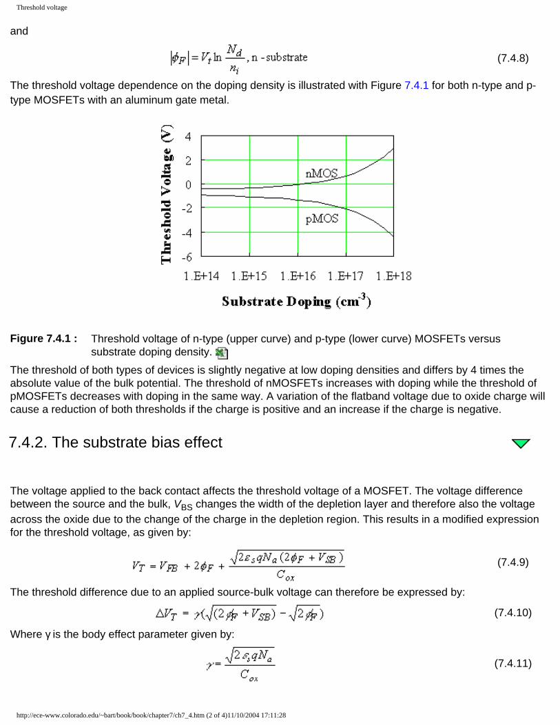
Threshold voltage
and
(7.4.8)
The threshold voltage dependence on the doping density is illustrated with Figure 7.4.1 for both n-type and p-type MOSFETs with an aluminum gate metal.
Figure 7.4.1 : Threshold voltage of n-type (upper curve) and p-type (lower curve) MOSFETs versus substrate doping density.
The threshold of both types of devices is slightly negative at low doping densities and differs by 4 times the absolute value of the bulk potential. The threshold of nMOSFETs increases with doping while the threshold of pMOSFETs decreases with doping in the same way. A variation of the flatband voltage due to oxide charge will cause a reduction of both thresholds if the charge is positive and an increase if the charge is negative.
7.4.2. The substrate bias effect
The voltage applied to the back contact affects the threshold voltage of a MOSFET. The voltage difference between the source and the bulk, VBS changes the width of the depletion layer and therefore also the voltage across the oxide due to the change of the charge in the depletion region. This results in a modified expression for the threshold voltage, as given by:
(7.4.9)
The threshold difference due to an applied source-bulk voltage can therefore be expressed by:
(7.4.10)
Where γ is the body effect parameter given by:
(7.4.11)
http://ece-www.colorado.edu/~bart/book/book/chapter7/ch7_4.htm (2 of 4)11/10/2004 17:11:28

Threshold voltage
The variation of the threshold voltage with the applied bulk-to-source voltage can be observed by plotting the transfer curve for different bulk-to-source voltages. The expected characteristics, as calculated using the quadratic model and the variable depletion layer model, are shown in Figure 7.4.2.
Figure 7.4.2 : Square root of ID versus the gate-source voltage as calculated using the quadratic model (upper curves) and the variable depletion layer model (lower curves).
A first observation is that the threshold shift is the same for both models. When biasing the device at the threshold voltage, drain saturation is obtained at zero drain-to-source voltage so that the depletion layer width is constant along the channel. As the drain-source voltage at saturation is increased, there is an increasing difference between the drain current as calculated with each model. The difference however reduces as a more negative bulk-source voltage is applied. This is due to the larger depletion layer width, which reduces the relative variation of the depletion layer charge along the channel.Example 7.3 Calculate the threshold voltage of a silicon nMOSFET when applying a substrate voltage, VBS
= 0, -2.5, -5, -7.5 and -10 V. The capacitor has a substrate doping Na = 1017 cm-3, a 20 nm thick oxide (εox = 3.9 ε0) and an aluminum gate (ΦM = 4.1 V). Assume there is no fixed charge in the oxide or at the oxide-silicon interface.
Solution The threshold voltage at VBS = -2.5 V equals:
Where the flatband voltage without substrate bias, VT0, was already calculated in example 6.2. The body effect parameter was obtained from:
http://ece-www.colorado.edu/~bart/book/book/chapter7/ch7_4.htm (3 of 4)11/10/2004 17:11:28

Threshold voltage
The threshold voltages for the different substrate voltages are listed in the table below.
http://ece-www.colorado.edu/~bart/book/book/chapter7/ch7_4.htm (4 of 4)11/10/2004 17:11:28
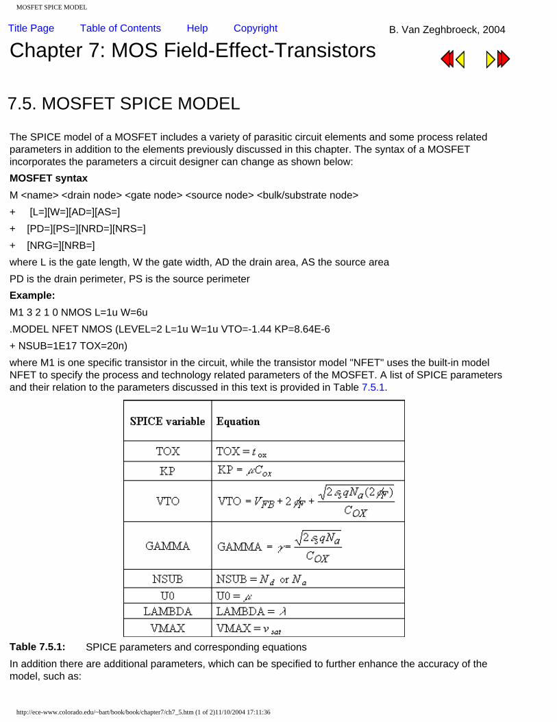
MOSFET SPICE MODEL
Title Page Table of Contents Help Copyright B. Van Zeghbroeck, 2004
Chapter 7: MOS Field-Effect-Transistors
7.5. MOSFET SPICE MODEL
The SPICE model of a MOSFET includes a variety of parasitic circuit elements and some process related parameters in addition to the elements previously discussed in this chapter. The syntax of a MOSFET incorporates the parameters a circuit designer can change as shown below:MOSFET syntaxM <name> <drain node> <gate node> <source node> <bulk/substrate node>+ [L=][W=][AD=][AS=]+ [PD=][PS=][NRD=][NRS=]+ [NRG=][NRB=]where L is the gate length, W the gate width, AD the drain area, AS the source areaPD is the drain perimeter, PS is the source perimeterExample:M1 3 2 1 0 NMOS L=1u W=6u.MODEL NFET NMOS (LEVEL=2 L=1u W=1u VTO=-1.44 KP=8.64E-6+ NSUB=1E17 TOX=20n)where M1 is one specific transistor in the circuit, while the transistor model "NFET" uses the built-in model NFET to specify the process and technology related parameters of the MOSFET. A list of SPICE parameters and their relation to the parameters discussed in this text is provided in Table 7.5.1.
Table 7.5.1: SPICE parameters and corresponding equationsIn addition there are additional parameters, which can be specified to further enhance the accuracy of the model, such as:
http://ece-www.colorado.edu/~bart/book/book/chapter7/ch7_5.htm (1 of 2)11/10/2004 17:11:36

MOSFET SPICE MODEL
LD , lateral diffusion (length) RD, drain ohmic resistance RG, gate ohmic resistance IS, bulk p-n saturation current CBD, bulk-drain zero-bias p-n capacitance CGSO/CGDO, gate-source/drain overlap capacitance/channel widthXJ, metallurgical junction depthWD, lateral diffusion (width)RS, source ohmic resistanceRB, bulk ohmic resistanceJS, bulk p-n saturation current/areaCBS, bulk-source zero-bias p-n capacitance
The gate-source/drain overlap capacitance per channel width is obtained from:
Where ∆L is the overlap between the gate and the source/drain region. The corresponding equivalent circuit is provided in Figure 7.5.1.
Figure 7.5.1 : Large signal model of a MOSFET
http://ece-www.colorado.edu/~bart/book/book/chapter7/ch7_5.htm (2 of 2)11/10/2004 17:11:36

MOSFET Circuits and Technology
Title Page Table of Contents Help Copyright B. Van Zeghbroeck, 2004
Chapter 7: MOS Field-Effect-Transistors
7.6. MOSFET Circuits and Technology7.6.1. MOSFET fabrication process7.6.2. Poly-silicon gate technology7.6.3. CMOS7.6.4. MOSFET Memory
MOSFET circuit technology has dramatically changed over the last three decades. Starting with a ten-micron pMOS process with an aluminum gate and a single metallization layer around 1970, the technology has evolved into a tenth-micron self-aligned-gate CMOS process with up to five metallization levels. The transition from dopant diffusion to ion implantation, from thermal oxidation to oxide deposition, from a metal gate to a poly-silicon gate, from wet chemical etching to dry etching and more recently from aluminum (with 2% copper) wiring to copper wiring has provided vastly superior analog and digital CMOS circuits.
7.6.1. MOSFET fabrication process
The MOSFET fabrication process has evolved dramatically over the years. Around 1970, pMOS circuits with aluminum gate metal and wiring were dominant. The corresponding steps of a typical pMOSFET fabrication process steps are listed in Table 7.6.1.
Table 7.6.1: pMOS process steps
http://ece-www.colorado.edu/~bart/book/book/chapter7/ch7_6.htm (1 of 8)11/10/2004 17:11:46
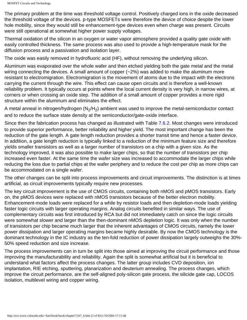
MOSFET Circuits and Technology
The primary problem at the time was threshold voltage control. Positively charged ions in the oxide decreased the threshold voltage of the devices. p-type MOSFETs were therefore the device of choice despite the lower hole mobility, since they would still be enhancement-type devices even when charge was present. Circuits were still operational at somewhat higher power supply voltages.Thermal oxidation of the silicon in an oxygen or water vapor atmosphere provided a quality gate oxide with easily controlled thickness. The same process was also used to provide a high-temperature mask for the diffusion process and a passivation and isolation layer. The oxide was easily removed in hydrofluoric acid (HF), without removing the underlying silicon.Aluminum was evaporated over the whole wafer and then etched yielding both the gate metal and the metal wiring connecting the devices. A small amount of copper (~2%) was added to make the aluminum more resistant to electromigration. Electromigration is the movement of atoms due to the impact with the electrons carrying the current through the wire. This effect can cause open circuits and is therefore a well-known reliability problem. It typically occurs at points where the local current density is very high, in narrow wires, at corners or when crossing an oxide step. The addition of a small amount of copper provides a more rigid structure within the aluminum and eliminates the effect.A metal anneal in nitrogen/hydrogen (N2/H2) ambient was used to improve the metal-semiconductor contact and to reduce the surface state density at the semiconductor/gate-oxide interface.Since then the fabrication process has changed as illustrated with Table 7.6.2. Most changes were introduced to provide superior performance, better reliability and higher yield. The most important change has been the reduction of the gate length. A gate length reduction provides a shorter transit time and hence a faster device. In addition, a gate length reduction is typically linked to a reduction of the minimum feature size and therefore yields smaller transistors as well as a larger number of transistors on a chip with a given size. As the technology improved, it was also possible to make larger chips, so that the number of transistors per chip increased even faster. At the same time the wafer size was increased to accommodate the larger chips while reducing the loss due to partial chips at the wafer periphery and to reduce the cost per chip as more chips can be accommodated on a single wafer.The other changes can be split into process improvements and circuit improvements. The distinction is at times artificial, as circuit improvements typically require new processes.The key circuit improvement is the use of CMOS circuits, containing both nMOS and pMOS transistors. Early on, the pMOS devices were replaced with nMOS transistors because of the better electron mobility. Enhancement-mode loads were replaced for a while by resistor loads and then depletion-mode loads yielding faster logic circuits with larger operating margins. Analog circuits benefited in similar ways. The use of complementary circuits was first introduced by RCA but did not immediately catch on since the logic circuits were somewhat slower and larger than the then-dominant nMOS depletion logic. It was only when the number of transistors per chip became much larger that the inherent advantages of CMOS circuits, namely the lower power dissipation and larger operating margins became highly desirable. By now the CMOS technology is the dominant technology in the IC industry as the ten-fold reduction of power dissipation largely outweighs the 30%-50% speed reduction and size increase.The process improvements can in turn be split into those aimed at improving the circuit performance and those improving the manufacturability and reliability. Again the split is somewhat artificial but it is beneficial to understand what factors affect the process changes. The latter group includes CVD deposition, ion implantation, RIE etching, sputtering, planarization and deuterium annealing. The process changes, which improve the circuit performance, are the self-aligned poly-silicon gate process, the silicide gate cap, LOCOS isolation, multilevel wiring and copper wiring.
http://ece-www.colorado.edu/~bart/book/book/chapter7/ch7_6.htm (2 of 8)11/10/2004 17:11:46

MOSFET Circuits and Technology
The self-aligned poly-silicon gate process was introduced before CMOS and marked the beginning of modern day MOSFETs. The self-aligned structure, as further discussed in section 7.6.2, is obtained by using the gate as the mask for the source-drain implant. Since the crystal damage caused by the high-energy ions must be annealed at high temperature (~800 C), an aluminum gate could no longer be used. Doped poly-silicon was found to be a very convenient gate material as it withstands the high anneal temperature and can be oxidized just like silicon. The self-aligned process lowers the parasitic capacitance between gate and drain and therefore improves the high-frequency performance and switching time. The addition of a silicide layer on top of the gate reduces the gate resistance while still providing a quality implant mask. The self-aligned process also reduced the transistor size and hence increased the density. The field oxide was replaced by a local oxidation isolation structure (LOCOS), where a Si3N4 layer is used to prevent the oxidation in the MOSFET region. The oxide provides an implant mask and contact hole mask yielding an even more compact device. Multilevel wiring is a necessity when one increases the number of transistors per chip since the number of wires increases with the square of the number of transistors and the average wire length increase linearly with the chip size. While multilevel wiring simply consists of a series of metal wiring levels separated by insulators, the multilevel wiring has increasingly become a bottleneck in the fabrication of high-performance circuits. Planarization techniques, as discussed below, and the introduction of copper instead of aluminum-based metals have further increased the wiring density and lowered the wiring resistance.
Table 7.6.2: MOS process changes and improvementsChemical vapor deposition (CDV) of insulating layers is now used instead of thermal oxidation since it does not consume the underlying silicon. Also because there is no limit to the obtainable thickness and since materials other than SiO2 (for instance Si3N4) can be deposited. CDV deposition is also frequently used to deposit refractory metals such as tungsten.Ion implantation has replaced diffusion because of the superior control and uniformity. Dry etching including plasma etching, reactive ion etching (RIE) and ion beam etching has replaced wet chemical etching. These etch processes provide better etch rate uniformity and control as well as pronounced anisotropic etching. The high etch rate selectivity of wet chemical etching is not obtained with these dry etch techniques, but are well compensated by the better uniformity.
http://ece-www.colorado.edu/~bart/book/book/chapter7/ch7_6.htm (3 of 8)11/10/2004 17:11:46

MOSFET Circuits and Technology
Sputtering of metals has completely replaced evaporation. Sputtering typically provides better adhesion and thickness control. It is also better suited to deposit refractory metals and silicides. Planarization is the process by which the top surface of the wafer is planarized after each step. The purpose of this planarization process is to provide a flat surface, so that fine-line lithography can be performed at all stages of the fabrication process. The planarization enables high-density multi-layer wiring levels. Deuterium anneal is a recent modification of the standard hydrogen anneal, which passivates the surface states. The change to deuterium was prompted because it is a heavier isotope of hydrogen. It chemically acts the same way but is less likely to be knocked out of place by the energetic carriers in the inversion layer. The use of deuterium therefore reduces the increase of the surface state density due to hot-electron impact.
7.6.2. Poly-silicon gate technology
An early improvement of the technology was obtained by using a poly-silicon gate, yielding a self-aligned structure which is both compact and has better performance. The poly-silicon gate is used as a mask during the implantation so that the source and drain regions are self-aligned with respect to the gate. This self-alignment structure reduces the device size. In addition, it eliminates the large overlap capacitance between gate and drain, while maintaining a continuous inversion layer between source and drain.A further improvement of this technique is the use of a low-doped drain (LDD) structure. As an example we consider the structure shown in Figure 7.6.1. Here a first shallow implant is used to contact the inversion layer underneath the gate. The shallow implant causes only a small overlap between the gate and source/drain regions. After adding a sidewall to the gate a second deep implant is added to the first one. This deep implant has a low sheet resistance and adds a minimal series resistance. The combination of the two implants therefore yields a minimal overlap capacitance and low access resistance.
http://ece-www.colorado.edu/~bart/book/book/chapter7/ch7_6.htm (4 of 8)11/10/2004 17:11:46

MOSFET Circuits and Technology
Figure 7.6.1: Cross-sectional view of a self-aligned poly-silicon gate transistor with LOCOS isolationShown is also the local oxidation isolation (LOCOS). Typically, there would also be an additional field and channel implant. The field implant increases the doping density under the oxide and thereby increases the threshold voltage of the parasitic transistor formed by the metal wiring on top of the isolation oxide. The channel implant provides an adjustment of the threshold voltage of the transistors. The use of a poly-silicon gate has the disadvantage that the sheet resistance of the gate is much larger than that of a metal gate. This leads to high RC time-constants of long poly-silicon lines. These long RC time-constants are reduced by using silicides (WSi, TaSi, CoSi etc.) instead or on top of poly-silicon. Also by using the poly-silicon only as gate material and not as a wiring level one can further eliminated such RC time delays.
7.6.3. CMOS
Complementary Metal-Oxide-Silicon circuits require an nMOS and pMOS transistor technology on the same substrate. To this end, an n-type well is provided in the p-type substrate. Alternatively one can use a p-well or both an n-type and p-type well in a low-doped substrate. The gate oxide, poly-silicon gate and source-drain contact metal are typically shared between the pMOS and nMOS technology, while the source-drain implants must be done separately. Since CMOS circuits contain pMOS devices, which are affected by the lower hole mobility, CMOS circuits are not faster than their all-nMOS counter parts. Even when scaling the size of the pMOS devices so that they provide the same current, the larger pMOS device has a higher capacitance.The CMOS advantage is that the output of a CMOS inverter can be as high as the power supply voltage and as low as ground. This large voltage swing and the steep transition between logic high and low yield large operation margins and therefore also a high circuit yield. In addition, there is no power dissipation in either logic state. Instead the power dissipation occurs only when a transition is made between logic states. CMOS circuits are therefore not faster than nMOS circuits but are more suited for very/ultra large-scale integration (VLSI/ULSI).CMOS circuits have one property, which is very undesirable, namely latchup. Latchup occurs when four alternating p and n-type regions are brought in close proximity. Together they form two bipolar transitors, one npn and one pnp transistor. The base of each transistor is connected to the collector of the other, forming a cross-coupled thyristor-like combination. As a current is applied to the base of one transistor, the current is amplified by the transistor and provided as the base current of the other one. If the product of the current gain of both transistors is larger than unity, the current through both devices increases until the series resistances of the circuit limits the current. Latchup therefore results in excessive power dissipation and faulty logic levels in the gates affected. In principle, this effect can be eliminated by separating n-type and p-type device. A more effective and less space-consuming solution is the use of trenches, which block the minority carrier flow. A deep and narrow trench is etched between all n-type and p-type wells, passivated and refilled with an insulating layer.
7.6.4. MOSFET Memory
MOSFET memory is an important application of MOSFETs. Memory chips contain the largest number of devices per unit area since the transistors are arranged in a very dense regular structure. The generic structure of a memory chip is shown in Figure 7.6.2.
http://ece-www.colorado.edu/~bart/book/book/chapter7/ch7_6.htm (5 of 8)11/10/2004 17:11:46

MOSFET Circuits and Technology
Figure 7.6.2: Arrangement of memory cells into an arrayA two dimensional array of memory cells, which store a single bit, are connected through a series of word lines and bit lines. One row of cells is activated by changing the voltage on the corresponding word line. The information is then stored in the cell by applying voltages to the bit lines. During a read operation, the information is retrieved by sensing the voltage on the bit lines with a sense amplifier. A possible implementation of a static random access memory (SRAM) is shown in Figure 7.6.3.
Figure 7.6.3: Static random access memory (SRAM) using a six-transistor cell.The memory cell consists of a flip-flop and the cells are accessed through two pass transistors connected to the bit lines and controlled by the word line. Depletion mode transistors are shown here as load devices. A common alternate load is an amorphous silicon resistor.A simpler cell leading to denser memory chips is the dynamic random access memory shown in Figure 7.6.4.
http://ece-www.colorado.edu/~bart/book/book/chapter7/ch7_6.htm (6 of 8)11/10/2004 17:11:46

MOSFET Circuits and Technology
Figure 7.6.4: Dynamic random access memory (DRAM) using a one-transistor cell.The dynamic cell contains only a single transistor and capacitor. The cell is called dynamic since the information is stored as charge on the capacitor. This charge slowly leaks away so that the cell needs to be refreshed periodically. The reading process is also destructive since the storage capacitor is discharged as a voltage is applied to the word line. Therefore, one has to rewrite the information into all the cells of a given row after reading a single cell from that row. Despite these restrictions, dynamic memory chips represent the largest section of the memory market. The advantage of a higher storage density outweighs all other considerations. Process advances such as the use of a vertical trench, have further increased the density of dynamic memory chips.As an example we now consider the dynamic memory cell shown in Figure 7.6.5. Shown are the top view and cross-sectional view. The figure illustrates how compact the cell can be by using the gate as the word line of the array and by using a trench capacitor. Also note that the drain of the transistor and one side of the capacitor are merged into one n-type region. The bit lines shown in the top view are placed next to the transistor for clarity. Actual memory cells have the bit lines on top of the transistors as shown in the cross-sectional view. More recent memory cells even have the transistor buried in the trench together with the capacitor.
http://ece-www.colorado.edu/~bart/book/book/chapter7/ch7_6.htm (7 of 8)11/10/2004 17:11:46

MOSFET Circuits and Technology
Figure 7.6.5: Dynamic random access memory (DRAM) using a one-transistor cell. (a) top view of four cells and (b) cross-sectional view of one cell.
A critical issue when scaling dynamic memory circuits is the capacitance of the storage capacitor. Scaling of all dimensions would yield a smaller value of the capacitor. However, larger arrays, made possible by scaling the device size, require a larger capacitance. After all, the critical operation in a dynamic memory is the read-out. During read-out, the memory capacitor is connected to the bit line and the charge is now distributed between the memory cell capacitance, the bit line capacitance and the parasitic capacitance of all the devices connected to the bit line. The remaining voltage on the bit line therefore depends on the ratio of the cell capacitance to that of the bit line and connected elements. In large memory chips the voltage would become unacceptably low if the memory capacitance would be scaled down with all other device dimensions. Instead the capacitance of the memory capacitor is kept almost constant from one generation to the next at a value around 1 fF. This value corresponds to the storage of 25,000 electrons at a voltage of 5 V and results in a bit line voltage of a few millivolts.
http://ece-www.colorado.edu/~bart/book/book/chapter7/ch7_6.htm (8 of 8)11/10/2004 17:11:46

Advanced MOSFET issues
Title Page Table of Contents Help Copyright B. Van Zeghbroeck, 2004
Chapter 7: MOS Field-Effect-Transistors
7.7. Advanced MOSFET issues7.7.1. Channel length modulation7.7.2. Drain induced barrier lowering7.7.3. Punch through7.7.4. Sub-threshold current7.7.5. Field dependent mobility7.7.6. Avalanche breakdown and parasitic bipolar action7.7.7. Velocity saturation7.7.8. Oxide Breakdown7.7.9. Scaling
7.7.1. Channel length modulation
Channel length modulation in a MOSFET is caused by the increase of the depletion layer width at the drain as the drain voltage is increased. This leads to a shorter channel length and an increased drain current. An example is shown in Figure 7.7.1. The channel-length-modulation effect typically increases in small devices with low-doped substrates. An extreme case of channel length modulation is punch through where the channel length reduces to zero. Proper scaling can reduce channel length modulation, namely by increasing the doping density as the gate length is reduces.
Figure 7.7.1: Current-Voltage characteristics of a MOSFET with and without channel length modulation. (Nd = 1017 cm-3, L = 1 µm)
http://ece-www.colorado.edu/~bart/book/book/chapter7/ch7_7.htm (1 of 5)11/10/2004 17:11:57

Advanced MOSFET issues
7.7.2. Drain induced barrier lowering
Drain induced barrier lowering (DIBL) is the effect a voltage of the drain has on the output conductance and measured threshold voltage. This effect occurs in devices where only the gate length is reduced without properly scaling the other dimensions. It is observed as a variation of the measured threshold voltage with reduced gate length. The threshold variation is caused by the increased current with increased drain voltage as the applied drain voltage controls the inversion layer charge at the drain, thereby competing with the gate voltage. This effect is due to the two-dimensional field distribution at the drain end and can typically be eliminated by properly scaling the drain and source depths while increasing the substrate doping density.
7.7.3. Punch through
Punch through in a MOSFET is an extreme case of channel length modulation where the depletion layers around the drain and source regions merge into a single depletion region. The field underneath the gate then becomes strongly dependent on the drain-source voltage, as is the drain current. Punch through causes a rapidly increasing current with increasing drain-source voltage. This effect is undesirable as it increases the output conductance and limits the maximum operating voltage of the device
7.7.4. Sub-threshold current
The basic assumption of the MOS capacitor analysis in section 6.3.2 is that no inversion layer charge exists below the threshold voltage. This leads to zero current below threshold. The actual sub-threshold current is not zero but reduces exponentially below the threshold voltage as:
(7.7.1)
with
(7.7.2)
The sub-threshold behavior is critical for dynamic circuits since one needs to ensure that no charge leaks through transistors biased below threshold.
7.7.4.1. Derivation of the sub-threshold ideality factor
The charge density below threshold can be expressed as:
(7.7.3)
Where the surface potential, φs, is related to the gate voltage by:
http://ece-www.colorado.edu/~bart/book/book/chapter7/ch7_7.htm (2 of 5)11/10/2004 17:11:57

Advanced MOSFET issues
(7.7.4)
The gate voltage, VG, is therefore related to the surface potential, φs, by:
(7.7.5)
Where the surface potential below threshold was approximated to its value, 2 φF, at threshold. The sub-threshold current therefore equals:
(7.7.6)
7.7.5. Field dependent mobility
The mobility is the inversion layer is distinctly lower than in bulk material. This is due to the fact the electron wavefunction extends into the oxide and the carrier mobility is lowered due to the lower mobility in the oxide. Higher electric fields at the surface - as typically obtained in scaled down devices - push the electron wavefunction even more into the oxide yielding a field dependent mobility. The mobility at the surface, µsurface,
varies with the electric field, , in the following way:
(7.7.7)
7.7.6. Avalanche breakdown and parasitic bipolar action
As the electric field in the channel is increased, avalanche breakdown occurs in the channel at the drain. This avalanche breakdown increases the current as in a p-n diode (see section 4.5.3 and 2.8). In addition, there is parasitic bipolar action taking place. Holes generated by the avalanche breakdown move from drain to source underneath the inversion layer. This hole current forward biases the source-bulk p-n diode so that now also electrons are injected as minority carriers into the p-type substrate underneath the inversion layer. These electrons arrive at the drain and again create more electron-hole pairs through avalanche multiplication. The positive feedback between the avalanche breakdown and the parasitic bipolar action results in breakdown at lower drain voltage.
7.7.7. Velocity saturation
http://ece-www.colorado.edu/~bart/book/book/chapter7/ch7_7.htm (3 of 5)11/10/2004 17:11:57
Advanced MOSFET issues
As devices are reduced in size, the electric field typically also increases and the carriers in the channel have an increased velocity. However at high fields there is no longer a linear relation between the electric field and the velocity as the velocity gradually saturates reaching the saturation velocity. This velocity saturation is caused by the increased scattering rate of highly energetic electrons, primarily due to optical phonon emission. This effect increases the transit time of carriers through the channel. In sub-micron MOSFETs one finds that the average electron velocity is larger than in bulk material so that velocity saturation is not quite as much of a restriction as initially thought.
7.7.8. Oxide Breakdown
As the gate-oxide is scaled down, breakdown of the oxide and oxide reliability becomes more of a concern. Higher fields in the oxide increase the tunneling of carriers from the channel into the oxide. These carriers slowly degrade the quality of the oxide and lead over time to failure of the oxide. This effect is referred to as time dependent destructive breakdown (TDDB).A simple reduction of the power supply voltage has been used to eliminate this effect. However as gate oxides approach a thickness of 1.5 - 3 nm, carrier tunneling becomes less dependent on the applied electric field so that this problem will require more attention.Oxides other than silicon dioxide have been considered as alternate oxides and are typically referred to as high-k dielectrics. These oxides have a larger dielectric constant so that the same gate capacitance can be obtained with a thicker oxide. The challenge is to obtain the same stability, reliability and breakdown voltage as silicon dioxide. Oxides of interest include Al2O3, ZrO and TiO.
7.7.9. Scaling
The reduction of the dimensions of a MOSFET has been has dramatic during the last three decades. Starting at a minimum feature length of 10 µm in 1970 the gate length was gradually reduced to 0.15 µm minimum feature size in 2000, resulting in a 13% reduction per year. Proper scaling of MOSFET however requires not only a size reduction of the gate length and width. It also requires a reduction of all other dimensions including the gate/source and gate/drain alignment, the oxide thickness and the depletion layer widths. Scaling of the depletion layer widths also implies scaling of the substrate doping density.Two types of scaling are common: constant field scaling and constant voltage scaling. Constant field scaling yields the largest reduction in the power delay product of a single transistor. However, it requires a reduction in the power supply voltage as one decreases the minimum feature size. Constant voltage scaling does not have this problem and is therefore the preferred scaling method since it provides voltage compatibility with older circuit technologies. The disadvantage of constant voltage scaling is that the electric field increases as the minimum feature length is reduced. This leads to velocity saturation, mobility degradation, increased leakage currents and lower breakdown voltages.The scaling of MOSFET device parameters is illustrated by Table 7.7.1 where constant field, constant voltage and constant voltage scaling in the presence of velocity saturation are compared.
http://ece-www.colorado.edu/~bart/book/book/chapter7/ch7_7.htm (4 of 5)11/10/2004 17:11:57

Advanced MOSFET issues
Table 7.7.1 : Comparison of the effect of scaling on MOSFET device parameters. Compared are constant field scaling, constant voltage scaling and constant voltage scaling in the presence of velocity overshoot.
http://ece-www.colorado.edu/~bart/book/book/chapter7/ch7_7.htm (5 of 5)11/10/2004 17:11:57

Advanced MOSFET issues
Title Page Table of Contents Help Copyright B. Van Zeghbroeck, 2004
Chapter 7: MOS Field-Effect-Transistors
7.8. Power MOSFETs Note:This is a temporary file, which is to be replaced with a fully hyperlinked HTML file. Meanwhile, the text can be accessed by clicking on the PDF icon.
http://ece-www.colorado.edu/~bart/book/book/chapter7/ch7_8.htm11/10/2004 17:12:10
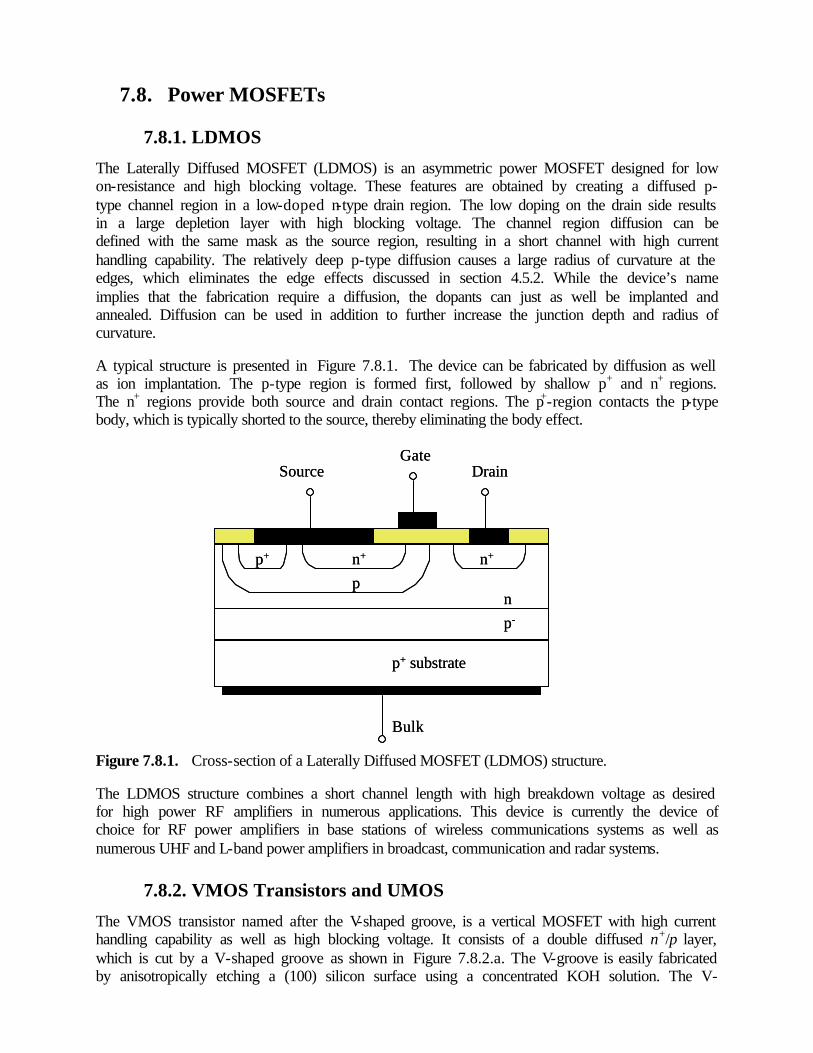
7.8. Power MOSFETs
7.8.1. LDMOS
The Laterally Diffused MOSFET (LDMOS) is an asymmetric power MOSFET designed for low on-resistance and high blocking voltage. These features are obtained by creating a diffused p-type channel region in a low-doped n-type drain region. The low doping on the drain side results in a large depletion layer with high blocking voltage. The channel region diffusion can be defined with the same mask as the source region, resulting in a short channel with high current handling capability. The relatively deep p-type diffusion causes a large radius of curvature at the edges, which eliminates the edge effects discussed in section 4.5.2. While the device’s name implies that the fabrication require a diffusion, the dopants can just as well be implanted and annealed. Diffusion can be used in addition to further increase the junction depth and radius of curvature.
A typical structure is presented in Figure 7.8.1. The device can be fabricated by diffusion as well as ion implantation. The p-type region is formed first, followed by shallow p+ and n+ regions. The n+ regions provide both source and drain contact regions. The p+-region contacts the p-type body, which is typically shorted to the source, thereby eliminating the body effect.
Figure 7.8.1. Cross-section of a Laterally Diffused MOSFET (LDMOS) structure.
The LDMOS structure combines a short channel length with high breakdown voltage as desired for high power RF amplifiers in numerous applications. This device is currently the device of choice for RF power amplifiers in base stations of wireless communications systems as well as numerous UHF and L-band power amplifiers in broadcast, communication and radar systems.
7.8.2. VMOS Transistors and UMOS
The VMOS transistor named after the V-shaped groove, is a vertical MOSFET with high current handling capability as well as high blocking voltage. It consists of a double diffused n+/p layer, which is cut by a V-shaped groove as shown in Figure 7.8.2.a. The V-groove is easily fabricated by anisotropically etching a (100) silicon surface using a concentrated KOH solution. The V-
p+ substrate
Bulk
p
Gate
p-
n+
n
Source Drain
p+ n+
p+ substrate
Bulk
p
Gate
p-
n+
n
Source Drain
p+ n+
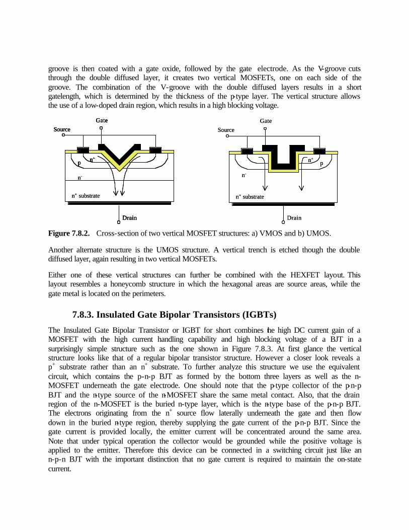
groove is then coated with a gate oxide, followed by the gate electrode. As the V-groove cuts through the double diffused layer, it creates two vertical MOSFETs, one on each side of the groove. The combination of the V-groove with the double diffused layers results in a short gatelength, which is determined by the thickness of the p-type layer. The vertical structure allows the use of a low-doped drain region, which results in a high blocking voltage.
Figure 7.8.2. Cross-section of two vertical MOSFET structures: a) VMOS and b) UMOS.
Another alternate structure is the UMOS structure. A vertical trench is etched though the double diffused layer, again resulting in two vertical MOSFETs.
Either one of these vertical structures can further be combined with the HEXFET layout. This layout resembles a honeycomb structure in which the hexagonal areas are source areas, while the gate metal is located on the perimeters.
7.8.3. Insulated Gate Bipolar Transistors (IGBTs)
The Insulated Gate Bipolar Transistor or IGBT for short combines the high DC current gain of a MOSFET with the high current handling capability and high blocking voltage of a BJT in a surprisingly simple structure such as the one shown in Figure 7.8.3. At first glance the vertical structure looks like that of a regular bipolar transistor structure. However a closer look reveals a p+ substrate rather than an n+ substrate. To further analyze this structure we use the equivalent circuit, which contains the p-n-p BJT as formed by the bottom three layers as well as the n-MOSFET underneath the gate electrode. One should note that the p-type collector of the p-n-p BJT and the n-type source of the n-MOSFET share the same metal contact. Also, that the drain region of the n-MOSFET is the buried n-type layer, which is the n-type base of the p-n-p BJT. The electrons originating from the n+ source flow laterally underneath the gate and then flow down in the buried n-type region, thereby supplying the gate current of the p-n-p BJT. Since the gate current is provided locally, the emitter current will be concentrated around the same area. Note that under typical operation the collector would be grounded while the positive voltage is applied to the emitter. Therefore this device can be connected in a switching circuit just like an n-p-n BJT with the important distinction that no gate current is required to maintain the on-state current.
n+ substrate
Drain
pn+
GateSource
n-
n+ substrate
Drain
pn+
GateSource
n-
Drain
p n+
GateSource
Drain
p n+
GateSource
n-
n+ substrate
Drain
p n+
GateSource
Drain
p n+
GateSource
n-
n+ substrate

Figure 7.8.3 Insulated Gate Bipolar Transistor (IGBT): a) equivalent circuit and b) device cross-section.
p substrate
Collector/Source
n
n+
Gate Collector/Source
n+p
Emitter (+V)
p
Emitter
Collector
Gate
Collector
p substrate
Collector/Source
n
n+
Gate Collector/Source
n+p
Emitter (+V)
p
Emitter
Collector
Gate
Collector

Advanced MOSFET issues
Title Page Table of Contents Help Copyright B. Van Zeghbroeck, 2004
Chapter 7: MOS Field-Effect-Transistors
7.9. High Electron Mobility Transistors (HEMTs) Note:This is a temporary file, which is to be replaced with a fully hyperlinked HTML file. Meanwhile, the text can be accessed by clicking on the PDF icon.
http://ece-www.colorado.edu/~bart/book/book/chapter7/ch7_9.htm11/10/2004 17:12:49
7.9. High Electron Mobility Transistors (HEMTs)
7.9.1. xxxx
xxxx
Figure 7.9.1 xxx

Chapter 7 examples
Title Page Table of Contents Help Copyright B. Van Zeghbroeck, 2004
Chapter 7: MOS Field-Effect-Transistors
Examples
Example 7.1 Calculate the drain current of a silicon nMOSFET with VT = 1 V, W = 10 µm, L = 1 µm and tox = 20 nm. The device is biased with VGS = 3 V and VDS = 5 V. Use the quadratic model, a surface mobility of 300 cm2/V-s and set VBS = 0 V.
Also calculate the transconductance at VGS = 3 V and VDS = 5 V and compare it to the output conductance at VGS = 3 V and VDS = 0 V.
Example 7.2 Repeat example 7.1 using the variable depletion layer model. Use VFB = -0.807 V and Na = 1017 cm-3.
Example 7.3 Calculate the threshold voltage of a silicon nMOSFET when applying a substrate voltage, VBS = 0, -2.5, -5, -7.5 and -10 V. The capacitor has a substrate doping Na = 1017 cm-3, a 20 nm thick oxide (εox = 3.9 ε0) and an aluminum gate (ΦM = 4.1 V). Assume there is no fixed charge in the oxide or at the oxide-silicon interface.
http://ece-www.colorado.edu/~bart/book/book/chapter7/ch7_ex.htm11/10/2004 17:13:11

Example 7.1 Calculate the drain current of a silicon nMOSFET with VT = 1 V, W = 10 µm, L = 1 µm and tox = 20 nm. The device is biased with VGS = 3 V and VDS = 5 V. Use the quadratic model, a surface mobility of 300 cm2/V-s and set VBS = 0 V. Also calculate the transconductance at VGS = 3 V and VDS = 5 V and compare it to the output conductance at VGS = 3 V and VDS = 0 V.
Solution The MOSFET is biased in saturation since VDS > VGS - VT. Therefore the drain current equals:
mA 04.12
)13(1
101020
1085.89.3300
2)(
2
7
14
2
=−
××
×××=
−=
−
−
TGSoxnD
VVL
WCI µ
The transconductance equals:
mS 04.1)13(1
101020
1085.89.3300
)(
7
14
=−××
×××=
−=
−
−
TGSoxnm VVL
WCg µ
and the output conductance equals:
mS 04.1)013(1
101020
1085.89.3300
)(
7
14
=−−××
×××=
−−=
−
−
DSTGSoxnd VVVLW
Cg µ

Example 7.2 Repeat example 7.1 using the variable depletion layer model. Use VFB = -0.807 V and Na = 1017 cm-3.
Solution To find out whether the MOSFET is biased in saturation, one first calculates the saturation voltage, VD,sat:
V 39.1
1)(21
2
2
2
,
=
−−+−
−−=
FBGBsa
ox
ox
sa
FFBGSsatDS
VVqNC
C
qN
VVV
εε
φ
The drain current is then obtained from:
mA 7.0
))2()2((232
)2
2(
2323
,,
=
+−+−
−−−=
SBFDBFasn
satDSsatDS
FFBGSoxn
D
VVqNLW
VV
VVL
WCI
φφεµ
φµ
The transconductance equals:
mS 52.0
]1)(21
2[
2
2
,
=
−−+−
−−=
FBGBsa
ox
ox
sa
FFBGSoxnsatm
VVqN
C
C
qN
VVL
WCg
εε
φµ
corresponding to a modified mobility µn* = 149 cm2/V-s.
The output conductance at VDS = 0 V equals:
mS 04.1==GSVDS
Dd V
Ig
∂∂
Which is the same as that of example 7.1 since the depletion layer width is constant for VDS = 0.

Example 7.3 Calculate the threshold voltage of a silicon nMOSFET when applying a substrate voltage, VBS = 0, -2.5, -5, -7.5 and -10 V. The capacitor has a substrate doping Na = 1017 cm-3, a 20 nm thick oxide (εox = 3.9 ε0) and an aluminum gate (ΦM = 4.1 V). Assume there is no fixed charge in the oxide or at the oxide-silicon interface.
Solution The threshold voltage at VBS = -2.5 V equals:
V 73.0)142.02
5.21(
42.0275.0
09.0
)12
1(2
0
=−×
+×
+−=
−++=F
SB
FTT
VVV
φφγ
Where the flatband voltage without substrate bias, VT0, was already calculated in example 6.2. The body effect parameter was obtained from:
1/2-
714
171914
V 75.0
1020/1085.89.3
10106.11085.89.1122
=
×××
××××××==
−−
−−
ox
as
C
qNεγ
The threshold voltages for the different substrate voltages are listed in the table below. VBS = -2.5 V -5 V -7.5 V -10 V VT 0.73 V 1.26 V 1.68 V 2.04 V

Principles of Semiconductor Devices
Title Page Table of Contents Help Copyright B. Van Zeghbroeck, 2004
Appendix:
Appendix 1: List of Symbols
Symbol Description MKS Units
A Area m2
c Speed of light in vacuum m/sC Capacitance per unit area F/m2
CFB Flatband capacitance per unit area of a MOS structure F/m2
Cj Junction capacitance per unit area F/m2
Cox Oxide capacitance per unit area F/m2
Dn Electron diffusion constant m2/sDp Hole diffusion constant m2/sE Energy JouleE Electric field V/mEa Acceptor energy JouleEc Conduction band energy of a semiconductor JouleEd Donor energy JouleEF Fermi energy (thermal equilibrium) JouleEg Energy bandgap of a semiconductor JouleEi Intrinsic Fermi energy JouleEv Valence band energy of a semiconductor Joule
Evacuum Electron energy in vacumm Joulef(E) Distribution function (probability density function) Fn Quasi-Fermi energy of electrons JouleFp Quasi-Fermi energy of holes Joule
gc(E) Density of states in the conduction band per unit energy and per unit volume m-3J-1
gv(E) Density of states in the valence band per unit energy and per unit volume m-3J-1
Gn Electron generation rate m-3s-1
Gp Hole generation rate m-3s-1
h Plank's constant JsReduced Plank's (= h /2π) Js
I Current AJ Current density A/m2
Jn Electron current density A/m2
Jp Hole current density A/m2
http://ece-www.colorado.edu/~bart/book/book/append/append1.htm (1 of 4)11/10/2004 17:13:35
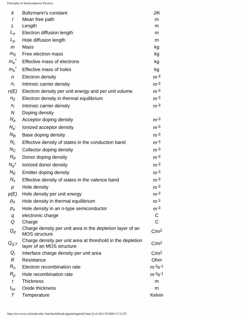
Principles of Semiconductor Devices
k Boltzmann's constant J/K l Mean free path mL Length mLn Electron diffusion length mLp Hole diffusion length mm Mass kgm0 Free electron mass kgme* Effective mass of electrons kgmh* Effective mass of holes kgn Electron density m-3
ni Intrinsic carrier density m-3
n(E) Electron density per unit energy and per unit volume m-3
n0 Electron density in thermal equilibrium m-3
ni Intrinsic carrier density m-3
N Doping density Na Acceptor doping density m-3
Na- Ionized acceptor density m-3
NB Base doping density m-3
Nc Effective density of states in the conduction band m-3
NC Collector doping density m-3
Nd Donor doping density m-3
Nd+ Ionized donor density m-3
NE Emitter doping density m-3
Nv Effective density of states in the valence band m-3
p Hole density m-3
p(E) Hole density per unit energy m-3
p0 Hole density in thermal equilibrium m-3
pn Hole density in an n-type semiconductor m-3
q electronic charge CQ Charge C
QdCharge density per unit area in the depletion layer of an MOS structure C/m2
Qd,TCharge density per unit area at threshold in the depletion layer of an MOS structure C/m2
Qi Interface charge density per unit area C/m2
R Resistance OhmRn Electron recombination rate m-3s-1
Rp Hole recombination rate m-3s-1
t Thickness mtox Oxide thickness mT Temperature Kelvin
http://ece-www.colorado.edu/~bart/book/book/append/append1.htm (2 of 4)11/10/2004 17:13:35

Principles of Semiconductor Devices
Un Net recombination rate of electrons m-3s-1
Up Net recombination rate of holes m-3s-1
v Velocity m/svth Thermal velocity m/sVa Applied voltage VVB Base voltage VVC Collector voltage VVD Drain voltage VVE Emitter voltage VVFB Flatband voltage VVG Gate voltage VVt Thermal voltage VVT Threshold voltage of an MOS structure Vw Depletion layer width mwB Base width mwC Collector width mwE Emitter width mwn Width of an n-type region mwp Width of a p-type region mx Position mxd Depletion layer width in an MOS structure m
xd,T Depletion layer width in an MOS structure at threshold mxj Junction depth mxn Depletion layer width in an n-type semiconductor mxp Depletion layer width in a p-type semiconductor m
α Transport factor β Current gain γ Body effect parameter V1/2
γE Emitter efficiency δ n Excess electron density m-3
δ p Excess hole density m-3
∆Qn,B Excess electron charge density in the base C/m2
εox Dielectric constant of the oxide F/mεs Dielectric constant of the semiconductor F/mµn Electron mobility m2/V-sµp Hole mobility m2/V-s
ρCharge density per unit volume
Resistivity
C/m3
Ωm
http://ece-www.colorado.edu/~bart/book/book/append/append1.htm (3 of 4)11/10/2004 17:13:35

Principles of Semiconductor Devices
ρox Charge density per unit volume in the oxide C/m3
σ Conductivity Ω−1m-1
τn Electron lifetime sτp Hole lifetime sφ Potential V
φB Barrier height VφF Bulk potential Vφi Built-in potential of a p-n diode or Schottky diode Vφs Potential at the semiconductor surface V
ΦM Workfunction of the metal V
ΦMSWorkfunction difference between the metal and the semiconductor V
ΦS Workfunction of the semiconductor Vχ Electron affinity of the semiconductor V
http://ece-www.colorado.edu/~bart/book/book/append/append1.htm (4 of 4)11/10/2004 17:13:35

Principles of Semiconductor Devices
Title Page Table of Contents Help Copyright B. Van Zeghbroeck, 2004
Appendix
Appendix 1: Symbol Index by NameA B C D E F G H I J K L M N O P Q R S T U V W X Y Z
Description Symbol MKS Units
- A - Acceptor doping density Na m-3
Acceptor energy Ea JouleApplied voltage Va VArea A m2
- B -
Barrier height φB VBase doping density NB m-3
Base voltage VB VBase width wB mBody effect parameter γ V1/2
Boltzmann's constant k J/K Built-in potential of a p-n diode or Schottky diode φi VBulk potential φF V
- C -
Capacitance per unit area C F/m2
Charge Q CCharge density per unit area at threshold in the depletion layer of an MOS structure
Qd,T C/m2
Charge density per unit area in the depletion layer of an MOS structure
Qd C/m2
Charge density per unit volume ρ C/m3
Charge density per unit volume in the oxide ρox C/m3
Collector doping density NC m-3
Collector voltage VC VCollector width wC mConduction band energy of a semiconductor Ec Joule
http://ece-www.colorado.edu/~bart/book/book/append/index.htm (1 of 5)11/10/2004 17:13:49

Principles of Semiconductor Devices
Conductivity σ Ω−1m-1
Current I ACurrent density J A/m2
Current gain β
- D -
Density of states in the conduction band per unit energy and per unit volume
gc(E) m-3J-1
Density of states in the valence band per unit energy and per unit volume
gv(E) m-3J-1
Depletion layer width w mDepletion layer width in a p-type semiconductor xp mDepletion layer width in an MOS structure xd mDepletion layer width in an MOS structure at threshold xd,T mDepletion layer width in an n-type semiconductor xn mDielectric constant of the oxide εox F/mDielectric constant of the semiconductor εs F/mDistribution function (probability density function) f(E) Donor doping density Nd m-3
Donor energy Ed JouleDoping density N Drain voltage VD V
- E -
Effective density of states in the conduction band Nc m-3
Effective density of states in the valence band Nv m-3
Effective mass of electrons me* kgEffective mass of holes mh* kgElectric field E V/mElectron affinity of the semiconductor χ VElectron current density Jn A/m2
Electron density n m-3
Electron density in thermal equilibrium n0 m-3
Electron density per unit energy and per unit volume n(E) m-3
Electron diffusion constant Dn m2/sElectron diffusion length Ln mElectron energy in vacumm Evacuum JouleElectron generation rate Gn m-3s-1
Electron lifetime τn sElectron mobility µn m2/V-s
http://ece-www.colorado.edu/~bart/book/book/append/index.htm (2 of 5)11/10/2004 17:13:49

Principles of Semiconductor Devices
Electron recombination rate Rn m-3s-1
electronic charge q CEmitter doping density NE m-3
Emitter efficiency γE Emitter voltage VE VEmitter width wE mEnergy E JouleEnergy bandgap of a semiconductor Eg JouleExcess electron charge density in the base ∆Qn,B C/m2
Excess electron density δ n m-3
Excess hole density δ p m-3
- F -
Fermi energy (thermal equilibrium) EF JouleFlatband capacitance per unit area of a MOS structure CFB F/m2
Flatband voltage VFB VFree electron mass m0 kg
- G -
Gate voltage VG V
- H -
Hole current density Jp A/m2
Hole density p m-3
Hole density in an n-type semiconductor pn m-3
Hole density in thermal equilibrium p0 m-3
Hole density per unit energy p(E) m-3
Hole diffusion constant Dp m2/sHole diffusion length Lp mHole generation rate Gp m-3s-1
Hole lifetime τp sHole mobility µp m2/V-sHole recombination rate Rp m-3s-1
- I -
Interface charge density per unit area QI C/m2
Intrinsic carrier density nI m-3
Intrinsic carrier density nI m-3
http://ece-www.colorado.edu/~bart/book/book/append/index.htm (3 of 5)11/10/2004 17:13:49

Principles of Semiconductor Devices
Intrinsic Fermi energy EI JouleIonized acceptor density Na- m-3
Ionized donor density Nd+ m-3
- J -
Junction capacitance per unit area Cj F/m2
Junction depth xj m
- K -
- L -
Length L m
- M -
Mass m kgMean free path l m
- N -
Net recombination rate of electrons Un m-3s-1
Net recombination rate of holes Up m-3s-1
- O -
Oxide capacitance per unit area Cox F/m2
Oxide thickness tox m
- P -
Plank's constant h JsPosition x mPotential φ VPotential at the semiconductor surface φs V
- Q -
Quasi-Fermi energy of electrons Fn JouleQuasi-Fermi energy of holes Fp Joule
- R -
http://ece-www.colorado.edu/~bart/book/book/append/index.htm (4 of 5)11/10/2004 17:13:49
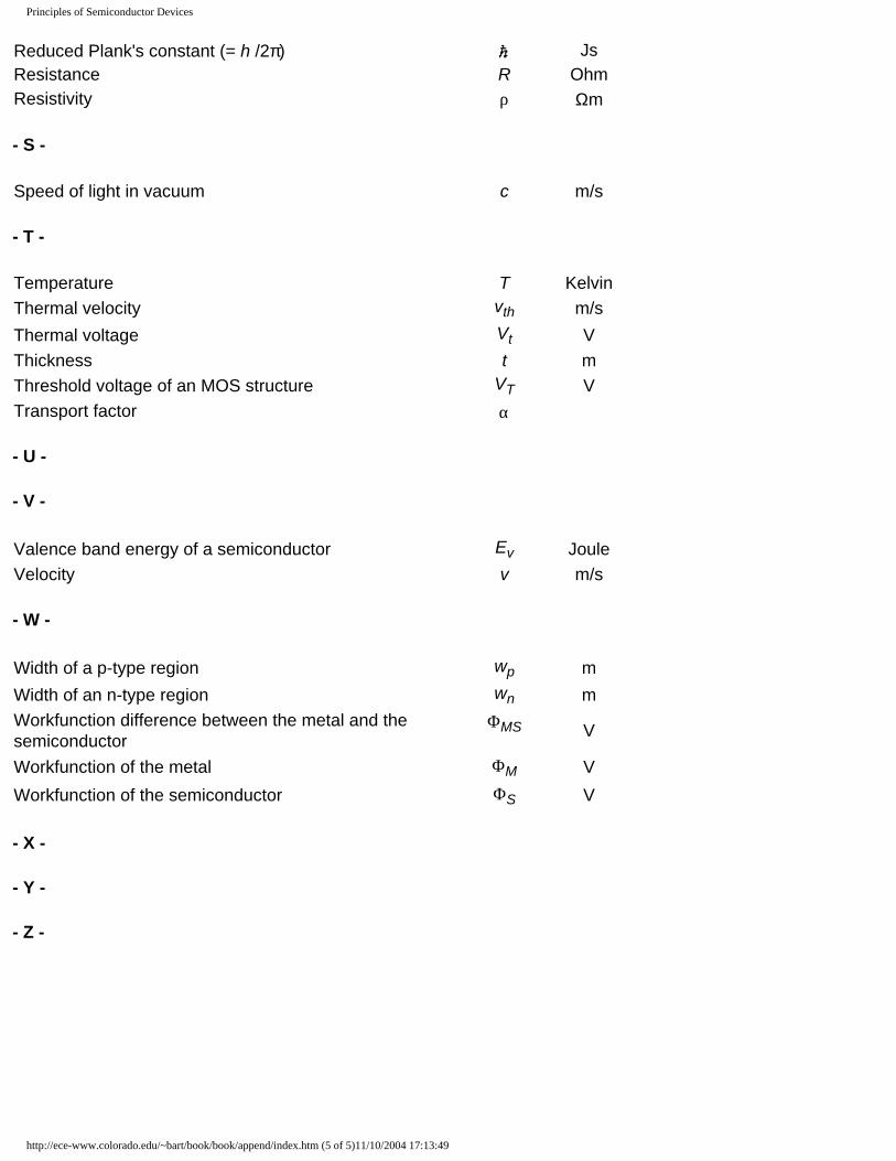
Principles of Semiconductor Devices
Reduced Plank's constant (= h /2π) JsResistance R OhmResistivity ρ Ωm
- S -
Speed of light in vacuum c m/s
- T -
Temperature T KelvinThermal velocity vth m/sThermal voltage Vt VThickness t mThreshold voltage of an MOS structure VT VTransport factor α
- U -
- V -
Valence band energy of a semiconductor Ev JouleVelocity v m/s
- W -
Width of a p-type region wp mWidth of an n-type region wn mWorkfunction difference between the metal and the semiconductor
ΦMS V
Workfunction of the metal ΦM VWorkfunction of the semiconductor ΦS V
- X -
- Y -
- Z -
http://ece-www.colorado.edu/~bart/book/book/append/index.htm (5 of 5)11/10/2004 17:13:49

Principles of Semiconductor Devices
Title Page Table of Contents Help Copyright B. Van Zeghbroeck, 2004
Appendix:
Appendix 1a: Extended List of Symbols Symbol Description MKS Units
a Acceleration m/s2
a0 Bohr radius mA Area m2
A* Richardson constant m/sAC Collector area m2
AE Emitter area m2
b Bimolecular recombination constant m3/sc Speed of light in vacuum m/sC Capacitance per unit area F/m2
CD Diffusion capacitance per unit area F/m2
CDS Drain-source capacitance FCFB Flatband capacitance per unit area of a MOS structure F/m2
CG Gate capacitance FCGS Gate-source capacitance FCGD Gate-drain capacitance F
CHFHigh-frequency capacitance per unit area of a MOS structure F/m2
Cj Junction capacitance per unit area F/m2
CLFLow-frequency (quasi-static) capacitance per unit area of a MOS structure F/m2
CM Miller capacitance FCox Oxide capacitance per unit area F/m2
Cs Semiconductor capacitance per unit area F/m2
Dn Electron diffusion constant m2/sDp Hole diffusion constant m2/sE Energy JouleE Electric field V/mE0 Lowest energy in a one-dimensional quantum well JouleEa Acceptor energy JouleEbr Breakdown field V/mEc Conduction band energy of a semiconductor JouleEd Donor energy JouleEF Fermi energy (thermal equilibrium) Joule
http://ece-www.colorado.edu/~bart/book/book/append/append1a.htm (1 of 7)11/10/2004 17:13:58

Principles of Semiconductor Devices
EF,n Fermi energy in an n-type semiconductor JouleEF,p Fermi energy in a p-type semiconductor JouleEg Energy bandgap of a semiconductor JouleEi Intrinsic Fermi energy JouleEn nth quantized energy JouleEph Photon energy JouleEt Trap energy JouleEv Valence band energy of a semiconductor Joule
Evacuum Electron energy in vacumm JouleF(E) Distribution function (probability density function)
fBE(E) Bose-Einstein distribution function fFD(E) Fermi-Dirac distribution function fMB(E) Maxwell-Boltzmann distribution function
F Force NewtonFn Quasi-Fermi energy of electrons JouleFp Quasi-Fermi energy of holes JoulegE) Density of states per unit energy and per unit volume m-3J-1
g(E) Density of states in the conduction band per unit energy and per unit volume m-3J-1
g(E) Density of states in the valence band per unit energy and per unit volume m-3J-1
gd Output conductance of a MOSFET Sgm Transconductance of a MOSFET SG Carrier generation rate m-3s-1
Gn Electron generation rate m-3s-1
Gp Hole generation rate m-3s-1
h Plank's constant JsReduced Plank's (= h /2π) Js
I Current AIB Base current of a bipolar transistor AIC Collector current of a bipolar transistor AID Drain current of a MOSFET AIE Emitter current of a bipolar transistor AIF Forward active current of a bipolar transistor A
ID,sat Drain current of a MOSFET in saturation AIph Photo current AIr Recombination current AIR Reverse active current of a bipolar transistor AIs Saturation current AIsc Short circuit current of a solar cell AJ Current density A/m2
http://ece-www.colorado.edu/~bart/book/book/append/append1a.htm (2 of 7)11/10/2004 17:13:58

Principles of Semiconductor Devices
Jn Electron current density A/m2
Jp Hole current density A/m2
k Boltzmann's constant wavenumber
J/K m-1
l Mean free path mL Length m
LD Debye length mLn Electron diffusion length mLp Hole diffusion length mLx Hole diffusion length mm Mass kgm* Effective mass kgmA Atomic mass kgm0 Free electron mass kgme* Effective mass of electrons kgmh* Effective mass of holes kg
M Proton massMultiplication factor kg
n
Electron densityIntegerRefractive indexIdeality factor
m-3
ni Intrinsic carrier density m-3
n(E) Electron density per unit energy and per unit volume m-3
n0 Electron density in thermal equilibrium m-3
ni Intrinsic carrier density m-3
nn Electron density in an n-type semiconductor m-3
nn0Thermal equilibrium electron density in an n-type semiconductor m-3
np Electron density in a p-type semiconductor m-3
np0Thermal equilibrium electron density in a p-type semiconductor m-3
N Number of particlesDoping density
Na Acceptor doping density m-3
Na- Ionized acceptor density m-3
NA Avogadro's number NB Base doping density m-3
Nc Effective density of states in the conduction band m-3
NC Collector doping density m-3
Nd Donor doping density m-3
Nd+ Ionized donor density m-3
http://ece-www.colorado.edu/~bart/book/book/append/append1a.htm (3 of 7)11/10/2004 17:13:58
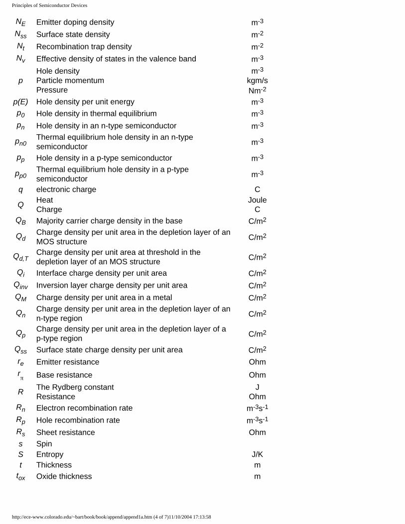
Principles of Semiconductor Devices
NE Emitter doping density m-3
Nss Surface state density m-2
Nt Recombination trap density m-2
Nv Effective density of states in the valence band m-3
pHole densityParticle momentumPressure
m-3
kgm/sNm-2
p(E) Hole density per unit energy m-3
p0 Hole density in thermal equilibrium m-3
pn Hole density in an n-type semiconductor m-3
pn0Thermal equilibrium hole density in an n-type semiconductor m-3
pp Hole density in a p-type semiconductor m-3
pp0Thermal equilibrium hole density in a p-type semiconductor m-3
q electronic charge C
Q HeatCharge
JouleC
QB Majority carrier charge density in the base C/m2
QdCharge density per unit area in the depletion layer of an MOS structure C/m2
Qd,TCharge density per unit area at threshold in the depletion layer of an MOS structure C/m2
Qi Interface charge density per unit area C/m2
Qinv Inversion layer charge density per unit area C/m2
QM Charge density per unit area in a metal C/m2
QnCharge density per unit area in the depletion layer of an n-type region C/m2
QpCharge density per unit area in the depletion layer of a p-type region C/m2
Qss Surface state charge density per unit area C/m2
re Emitter resistance Ohmrπ Base resistance Ohm
R The Rydberg constantResistance
JOhm
Rn Electron recombination rate m-3s-1
Rp Hole recombination rate m-3s-1
Rs Sheet resistance Ohms Spin S Entropy J/Kt Thickness m
tox Oxide thickness m
http://ece-www.colorado.edu/~bart/book/book/append/append1a.htm (4 of 7)11/10/2004 17:13:58

Principles of Semiconductor Devices
T TemperatureKinetic energy
KelvinJoule
uω Spectral density Jm-3s-1
U Total energy JouleUA Auger recombination rate m-3s-1
Ub-b Band-to-band recombination rate m-3s-1
Un Net recombination rate of electrons m-3s-1
Up Net recombination rate of holes m-3s-1
USHR Shockley-Read-Hall recombination rate m-3s-1
v Velocity m/svR Richardson velocity m/svsat Saturation velocity m/svth Thermal velocity m/s
V Potential energyVolume
Joulem3
Va Applied voltage VVA Early voltage VVbr Breakdown voltage VVB Base voltage VVBE Base-emitter voltage VVBC Base-collector voltage VVC Collector voltage VVCE Collector-emitter voltage VVD Drain voltage VVDS Drain-source voltage V
VDS,sat Drain-source saturation voltage VVE Emitter voltage VVFB Flatband voltage VVG Gate voltage VVGS Gate-source voltage VVoc Open circuit voltage of a solar cell VVt Thermal voltage VVT Threshold voltage of an MOS structure Vw Depletion layer width mwB Base width mwC Collector width mwE Emitter width mwn Width of an n-type region mwp Width of a p-type region mW Work Joule
http://ece-www.colorado.edu/~bart/book/book/append/append1a.htm (5 of 7)11/10/2004 17:13:58

Principles of Semiconductor Devices
x Position mxd Depletion layer width in an MOS structure m
xd,T Depletion layer width in an MOS structure at threshold mxj Junction depth mxn Depletion layer width in an n-type semiconductor mxp Depletion layer width in a p-type semiconductor m
αAbsorption coefficientTransport factor m-1
αF Forward active transport factor αn Ionization rate coefficient for electrons m-1 αR Reverse active transport factor αT Base transport factor β Current gain γ Body effect parameter V1/2
γE Emitter efficiency Γn Auger coefficient for electrons m6s-1 Γp Auger coefficient for holes m6s-1 δ n Excess electron density m-3 δ p Excess hole density m-3 δ R Depletion layer recombination factor
∆Qn,B Excess electron charge density in the base C/m2 ε Dielectric constant F/m ε0 Permittivity of vacuum F/m εox Dielectric constant of the oxide F/m εs Dielectric constant of the semiconductor F/mµ0 Permeability of vacuum H/m Θ Tunnel probability λ Wavelength m µ Electro-chemical potential Joule µn Electron mobility m2/V-s µp Hole mobility m2/V-s ν Frequency Hz
ρCharge density per unit volumeResistivity
C/m3
Ωm
ρox Charge density per unit volume in the oxide C/m3 σ Conductivity Ω−1m-1 τ Scattering time s τn Electron lifetime s τp Hole lifetime s φ Potential V
http://ece-www.colorado.edu/~bart/book/book/append/append1a.htm (6 of 7)11/10/2004 17:13:58
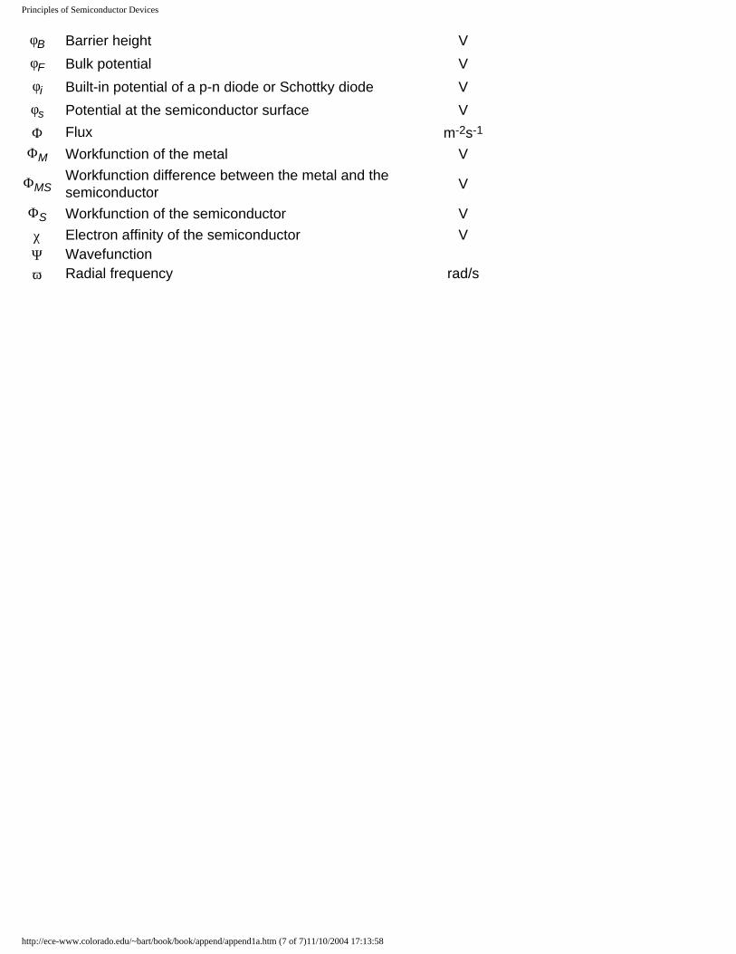
Principles of Semiconductor Devices
φB Barrier height V φF Bulk potential V φi Built-in potential of a p-n diode or Schottky diode V φs Potential at the semiconductor surface V Φ Flux m-2s-1
ΦM Workfunction of the metal V
ΦMSWorkfunction difference between the metal and the semiconductor V
ΦS Workfunction of the semiconductor V χ Electron affinity of the semiconductor V Ψ Wavefunction ω Radial frequency rad/s
http://ece-www.colorado.edu/~bart/book/book/append/append1a.htm (7 of 7)11/10/2004 17:13:58

Appendix 2
Title Page Table of Contents Help Copyright B. Van Zeghbroeck, 2004
Appendix:
Appendix 2: Physical Constants
Avogadro's number NA 6.022 x 10²³ atoms per mole
Bohr radius a0 52.9177 picometer
0.529177 Angstrom
Boltzmann's constant k 1.38 x 10⁻²³ Joule/Kelvin
8.62 x 10⁻⁵ electron Volt/Kelvin
Electronic charge q 1.602 x 10⁻¹⁹ Coulomb
Free electron rest mass m0 9.11 x 10⁻³¹ kilogram
5.69 x 10⁻¹⁶ eV s2 cm-2
Permeability of free space µ0 4π x 10-7 Henry/meter
Permittivity of free space ε0 8.854 x 10⁻¹² Farad/meter
8.854 x 10⁻¹⁴ Farad/centimeter
Planck's constant h 6.625 x 10⁻³⁴ Joule second
4.134 x 10⁻¹⁵ electron Volt second
Reduced Planck's constant 1.054 x 10⁻³⁴ Joule second
Proton rest mass M 1.67 x 10⁻²⁷ Kilogram
Rydberg constant R 2.17991 x 10⁻¹⁸ Joule
13.6058 electron Volt
Speed of light in vacuum c 2.998 x 10⁸ meter/second
2.998 x 10¹⁰ centimeter/second
Thermal voltage (at T = 300 K) 25.86 milliVolt
http://ece-www.colorado.edu/~bart/book/book/append/append2.htm11/10/2004 17:14:10

Appendix 3
Title Page Table of Contents Help Copyright B. Van Zeghbroeck, 2004
Appendix:
Appendix 3: Material Parameters
Name Symbol Germanium Silicon Gallium Arsenide
Bandgap energy at 300 K Eg (eV) 0.66 1.12 1.424
Breakdown Field Ebr (V/cm) 105 3 x 105 * 4 x 105
Density (g/cm3) 5.33 2.33 5.32
Effective density of states in the conduction band at 300 K
Nc (cm-3) 1.02 x 10¹⁹ 2.82 x 10¹⁹ 4.35 x 10¹⁷
Effective density of states in the valence band at 300 K
Nv (cm-3) 5.65 x 10¹⁸ 1.83 x 10¹⁹ 7.57 x 10¹⁸
Intrinsic concentration at 300 K ni (cm-3) 2.8 x 10¹³ 1.0 x 10¹⁰ 2.0 x 10⁶
Effective mass for density of states calculations
Electrons me* / m0 0.55 1.08 0.067
Holes mh* / m0 0.37 0.81 0.45
Electron affinity χ (V) 4.0 4.05 4.07
Lattice constant a (pm) 564.613 543.095 565.33
Mobility at 300 K (undoped)
Electrons µn (cm2/V-s) 3900 1400† 8800
Holes µp (cm2/V-s) 1900 450† 400
Relative dielectric constant εs/ ε0 16 11.9 13.1
Thermal conductivity at 300 K χ (W/cmK) 0.6 1.5 0.46
http://ece-www.colorado.edu/~bart/book/book/append/append3.htm (1 of 2)11/10/2004 17:14:19

Appendix 3
Refractive index at 632.8 nm wavelength
n 5.441
- i 0.785
3.875
- i 0.0181
3.856
- i 0.196
*See also section 4.5.1: Breakdown field in silicon at 300 K
†See also section 2.7.2: Mobility of doped silicon at 300 K
http://ece-www.colorado.edu/~bart/book/book/append/append3.htm (2 of 2)11/10/2004 17:14:19

Appendix 4
Title Page Table of Contents Help Copyright B. Van Zeghbroeck, 2004
Appendix:
Appendix 4: Prefixes
deci (d) 10-1 deka (da) 101
centi (c) 10-2 hecto (h) 102
milli (m) 10-3 kilo (k) 103
micro (m) 10-6 mega (M) 106
nano (n) 10-9 giga (G) 109
pico (p) 10-12 tera (T) 1012
femto (f) 10-15 peta (P) 1015
atto (a) 10-18 exa (X) 1018
http://ece-www.colorado.edu/~bart/book/book/append/append4.htm11/10/2004 17:14:25

Appendix 5
Title Page Table of Contents Help Copyright B. Van Zeghbroeck, 2004
Appendix:
Appendix 5: Units
MKS Units
Unit Symbol Variable Symbol MKSA unitsAmpere A Current I fundamental MKSA unitCoulomb C Charge Q Ampere secondFarad F Capacitance C Coulomb Volt-1 = Joule Volt-2
Henry H Inductance L Weber Ampere-1 = Tesla meter2 Ampere-1
Joule J Energy E Newton meter = kilogram meter2 second-2
Kelvin K Temperature T fundamental MKSA unitkilogram kg Mass m fundamental MKSA unitmeter m Length L fundamental MKSA unitNewton N Force F kilogram meter second-2
Ohm Ω Resistance R Volt Ampere-1 = Volt2 Joule-1 second-1
Pascal P Pressure P Newton meter-2
second s time t fundamental MKSA unitSiemens S conductance G Ampere Volt-1 = Joule second Volt-2
Tesla T Magnetic field BNewton Ampere-1 meter-1 = Joule Ampere-1 meter-2 = Volt second meter-2
Volt V potential φ Joule coulomb-1
Watt W Power P Joule second-1
Weber Wb Magnetic flux Φ Tesla meter2 = Volt second
non-MKS Units
Electron Volt (Unit of energy) = 1.602 x 10⁻¹⁹ Joule
moles/liter (Unit of concentration) = 6.022 x 1020 cm-3
Degrees Centigrade (Unit of Temperature) = -273.16 + T(in Kelvin)
Inch (Unit of Length) = 2.54 cm
mil or milli inch (Unit of Length) = 25.4 micrometer
http://ece-www.colorado.edu/~bart/book/book/append/append5.htm (1 of 2)11/10/2004 17:14:31
Appendix 5
A or Angstrom (Unit of Length) = 0.1 nm
http://ece-www.colorado.edu/~bart/book/book/append/append5.htm (2 of 2)11/10/2004 17:14:31

Appendix 6
Title Page Table of Contents Help Copyright B. Van Zeghbroeck, 2004
Appendix:
Appendix 6: The Greek Alphabet
α Α alpha ν Ν nuβ Β beta ξ Ξ xiγ Γ gamma ο Ο omicronδ ∆ delta π Π piε Ε epsilon ρ Ρ rhoζ Ζ zeta σ Σ sigmaη Η eta τ Τ tauθ Θ theta υ Υ upsilonι Ι iota φ Φ phiκ Κ kappa ξ Ξ chiλ Λ lambda ψ Ψ psiµ Μ mu ω Ω omega
http://ece-www.colorado.edu/~bart/book/book/append/append6.htm11/10/2004 17:14:38
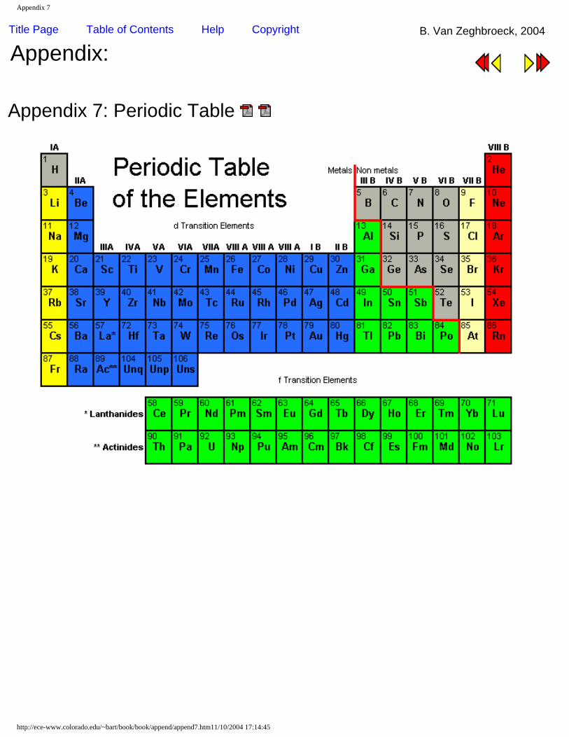
Appendix 7
Title Page Table of Contents Help Copyright B. Van Zeghbroeck, 2004
Appendix:
Appendix 7: Periodic Table
http://ece-www.colorado.edu/~bart/book/book/append/append7.htm11/10/2004 17:14:45

Appendix 8
Title Page Table of Contents Help Copyright B. Van Zeghbroeck, 2004
Appendix:
Appendix 8: Numeric answers to selected problems Spreadsheet with predefined physical constants and material parameters
Chapter 1
1. 0.62 µm, 0.87 nm 2. 1.55 eV, 375 THz, 4 x 10¹⁸ 3. 4. 16.5 µm 5. 6. 3.88 nm 7. -13.6 eV, -3.4 eV, -1.51 eV 8. 9. 10. 0.11 eV, 0.56 eV and 0.79 eV 11. 12. 172 meV 13. 138 meV
Chapter 2
1. 52.36%, 68.02%, 74.05%, 34.01% 2. 406.3°C 3. 4. 0.0099 5. 6.29 x 10⁻⁵, 0.045, 484.7°C 6. 1.02 x 10¹⁹, 5.65 x 10¹⁸; 2.82 x 10¹⁹, 1.83 x 10¹⁹; 4.37 x 10¹⁷, 7.57 x 1018 cm-3 1.42 x 10¹⁹, 7.83 x 10¹⁸; 3.91 x 10¹⁹, 2.54 x 10¹⁹; 6.04 x 10¹⁷, 1.05 x 1019 cm-3 7. 2.16 x 10¹³, 8.81 x 10⁹, 1.97 x 10⁶; 3.67 x 10¹⁴, 8.55 x 10¹¹, 6.04 x 108 cm-3 8. -7.68 meV, -5.58 meV, 36.91 meV -9.56 meV, -6.94 meV, 45.92 meV 9. 2.24 x 10¹⁸, 1.48 x 10⁸; 1.60 x 10¹⁵, 1.32 x 10⁵; 2.23 x 10¹¹, 18.4 cm-3 9.27 x 10¹³, 4.45 x 10¹²; 6.02 x 10¹⁴, 3.50 x 10⁵; 3.97 x 10¹², 1.04 cm-3 10. 11. 104 cm-3, 0.357 eV
http://ece-www.colorado.edu/~bart/book/book/append/append8.htm (1 of 3)11/10/2004 17:15:32

Appendix 8
12. 1012 cm-3, 108 cm-3 13. 9.17 x 10¹⁴, 9.15 x 10¹⁴, 2.76 x 1015 cm-3 14. 7.59 x 1016 cm-3 15. 2.77 x 1019 cm-3s-1, 2.77 x 1015 cm-3, 2.77 x 1015 cm-3, 417 meV, -324 meV 16. 1013 cm-3s-1, 10-3 s 17. 2.96 x 10⁻⁶ cm/Ohm, 337 kOhm-cm 18. 393 kOhm-cm, 5.67 x 10⁹, 1.76 x 10¹⁰, 1.20 x 1010 cm-3 19. 18, 42, 60 meV 20. 2.42 nm 21. 2.42 x 1021 cm-3eV-1 22. 4.74 %, 95.26 % 23. 24. 1.39 25. 30 kV/cm, 15 V, 16.7 ps 26. 8.92 x 1014 cm-3, 6.94 x 1015 cm-3 27. 0.455 mm 28. 2111 cm2/V-s 29. 1.05 cm-3J-1, 9.14 x 10⁻⁴ 30. 0.53 Ω-cm, 2.1 x 10⁻⁷, 0.22 Ω-cm, 123 meV 31. 1016 cm-3, 104 cm-3, -357 meV 1015 cm-3, 105 cm-3, 298 meV 32. 828 A/cm2
Chapter 3
1. 1.84 x 1017cm-3, 75 nm, 737 kV/cm
2.
3. 6.24 x 10⁻⁷cm2
4. 154-269 MHz
Chapter 4
1. 0.75 V, 785 nm, -95.5 kV/cm
2. 104, 1016, 9 x 10¹⁶, 1.11 x 103cm-3; 0.771 V; 0.729 V;
3. -12.4 kV/cm, 1.65 x 1016cm-3
4. 0.76 V; 0.35, 0.20, 0.72 micron; -43.8, -25.5, -90.8 kV/cm; 0.13, 0.04, 0.54 V;
5. 1.71 x 1015cm-3, 0.76 V, 5.91 x 109cm-3
6. 2.84 x 1014cm-3
7. 3.27 x 1017cm-3, 8.22 x 1016cm-3, 0.86 V, -49 V 8. 7.6 x 10¹⁵, 492 nm, 21.4 nF/cm2, 28 kV/cm
4.4 x 10¹⁴, 1.3 x 10¹⁶, 528 nm, 20 nF/cm2, 26.5 kV/cm
http://ece-www.colorado.edu/~bart/book/book/append/append8.htm (2 of 3)11/10/2004 17:15:32
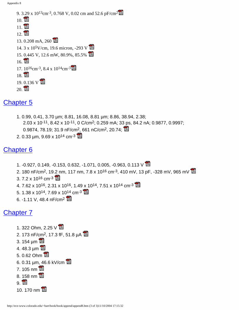
Appendix 8
9. 3.29 x 1013cm-3, 0.768 V, 0.02 cm and 52.6 pF/cm2
10.
11.
12.
13. 0.208 mA, 260
14. 3 x 10⁵V/cm, 19.6 micron, -293 V
15. 0.445 V, 12.6 mW, 80.9%, 85.5%
16.
17. 1016cm-3, 8.4 x 1014cm-3
18.
19. 0.136 V
20.
Chapter 5
1. 0.99, 0.41, 3.70 µm; 8.81, 16.08, 8.81 µm; 8.86, 38.94, 2.38; 2.03 x 10⁻¹¹, 8.42 x 10⁻¹¹, 0 C/cm2; 0.259 mA; 33 ps, 84.2 nA; 0.9877, 0.9997; 0.9874, 78.19; 31.9 nF/cm2, 661 nC/cm2, 20.74; 2. 0.33 µm, 9.69 x 1014 cm-3
Chapter 6
1. -0.927, 0.149, -0.153, 0.632, -1.071, 0.005, -0.963, 0.113 V 2. 180 nF/cm2, 19.2 nm, 117 nm, 7.8 x 1016 cm-3, 410 mV, 13 pF, -328 mV, 965 mV 3. 7.2 x 1016 cm-3 4. 7.62 x 10¹⁶, 2.31 x 10¹⁶, 1.49 x 10¹⁴, 7.51 x 1014 cm-3 5. 1.38 x 10¹⁴, 7.69 x 1014 cm-3 6. -1.11 V, 48.4 nF/cm2
Chapter 7
1. 322 Ohm, 2.25 V 2. 173 nF/cm2, 17.3 fF, 51.8 µA 3. 154 µm 4. 48.3 µm 5. 0.62 Ohm 6. 0.31 µm, 46.6 kV/cm 7. 105 nm 8. 158 nm 9. 10. 170 nm
http://ece-www.colorado.edu/~bart/book/book/append/append8.htm (3 of 3)11/10/2004 17:15:32

Problem 3.1 Consider a gold-GaAs Schottky diode with a capacitance of 1 pF at -1 V. What is the doping density of the GaAs? Also calculate the depletion layer width at zero bias and the field at the surface of the semiconductor at -10 V. The area of the diode is 10-5 cm2.
Solution The depletion layer width can be calculated from the capacitance yielding:
==C
Ax s
d
ε=
×××−
−−
12
514
101010854.81.13
0.116 µm
From this one can find the doping density:
=−
=2
)(2
d
aisd qx
VN
φε2519
14
)1016.1(106.1)1(10854.81.132
−−
−
×××+×××× iφ
Provided one knows the built-in potential
=−=d
ctBi N
NV lnφφ
dN
171035.4ln0259.007.48.4
×−−
Which in turn depends on the doping density. Starting with φi = 0.7 one finds Nd = 1.83 x 1017 cm-3 and the corresponding built-in potential φi = 0.708. Further iteration yields the result: Nd = 1.84 x 1017 cm-3. The depletion layer width at zero bias equals:
=−
=d
aisd qN
Vx
)(2 φε
=×××
−××××−
−
1719
14
1084.1106.1)0708.0(10854.81.132
0.075 µm
And the electric field at the surface for Va = -10 V equals:
=−
===s
dai
s
dd qNVxqNx
εφ
ε)(2
)0(E
=××
×××××−
−
14
1719
10854.81.131084.106.17.102
737 kV/cm

Problem 3.2 Using the work functions listed in table 3.2.1, predict which
metal-semiconductor junctions are expected to be ohmic contacts. Use the ideal interface model. The barrier height on an n-type semiconductor is given by
χφ −Φ= MB And on a p-type semiconductor by
Mg
B q
EΦ−+= χφ
Using the metal workfunction from table 3.2.1 and the semiconductor electron affinity and bandgap from appendix 3 one finds that only three combinations yield a negative barrier height as provided in the table below. One expects these metal-semiconductor junctions to yield an ohmic contact. Au/p-Ge -0.14 V
Pt/p-Ge -0.64 V
Solution
Pt/p-Si -0.13 V

Problem 3.3 Design a platinum-silicon diode with a capacitance of 1 pF and a
maximum electric field less than 104 V/cm at -10 V bias. Provide a possible doping density and area. Make sure the diode has an area between 10-5 and 10-7 cm2. Is it possible to satisfy all requirements if the doping density equals 1017 cm-3? What is the corresponding area?
Solution From the capacitance and the area one finds the corresponding depletion layer width, namely:
j
sd C
xε
= = 105 nm and 1.05 nm
corresponding to a diode area of 10-5 and 10-7 cm2 respectively. Note that the capacitance Cj is the capacitance per unit area. The corresponding doping density is obtain from:
d
sd qx
xN
ε)0( ==
E= 6.24 x 10¹⁵ and 6.24 x 1017 cm-3 respectively
Any other designs should have a doping density between those two values. Since the doping density of 1017 cm-3 is also between those two values it is a possible solution. The corresponding area is 6.24 x 10⁻⁷ cm2.

Problem 3.4 A platinum-silicon diode (area = 10-4 cm-2, Nd =1017 cm-3) is
part of an LC tuning circuit containing a 100 nH inductance. The applied voltage must be less than 5 V. What is the tuning range
of the circuit? The resonant frequency equals LCπ
ν2
1= ,
where L is the inductance and C is the diode capacitance. Solution The capacitance of the diode per unit area equals:
)(2 ai
dsj V
NqC
−=
φε
= 10.7 and 3.5 pF at 0 and –5 V respectively
Where the built-in potential is calculated from:
c
dtBi N
NV ln−= φφ = 732 mV
The resonant frequency therefore can be tuned from 154 MHz to 269 MHz.

Problem 4.1 An abrupt silicon p-n junction (Na = 1016 cm-3 and Nd = 4 x 1016 cm-3) is biased with Va = -3 V. Calculate the built-in potential, the depletion layer width and the maximum electric field of the junction.
Solution The built-in potential is calculated from:
2lni
adti n
NNV=φ = 0.75 V
The depletion layer width equals
))(11
(2
aida
sd V
NNqx −+= φ
ε= 0.785 µm
And the maximum electric field equals
d
ai
xV
x)(2
)0(−
−==φ
E = -95.5 kV/cm
Note that mathematically the maximum field is zero since the field is negative. However, the sign indicates the direction of the field and depends merely on convention.
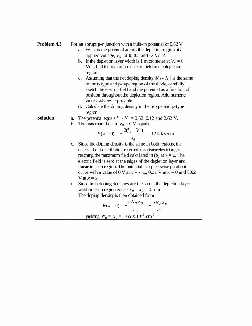
Problem 4.3 For an abrupt p-n junction with a built-in potential of 0.62 V
a. What is the potential across the depletion region at an applied voltage, Va, of 0, 0.5 and -2 Volt?
b. If the depletion layer width is 1 micrometer at Va = 0 Volt, find the maximum electric field in the depletion region.
c. Assuming that the net doping density |Nd - Na| is the same in the n-type and p-type region of the diode, carefully sketch the electric field and the potential as a function of position throughout the depletion region. Add numeric values wherever possible.
d. Calculate the doping density in the n-type and p-type region
Solution a. The potential equals φi - Va = 0.62, 0.12 and 2.62 V. b. The maximum field at Va = 0 V equals
d
ai
xV
x)(2
)0(−
−==φ
E = - 12.4 kV/cm
c. Since the doping density is the same in both regions, the electric field distribution resembles an isosceles triangle reaching the maximum field calculated in (b) at x = 0. The electric field is zero at the edges of the depletion layer and linear in each region. The potential is a piecewise parabolic curve with a value of 0 V at x = - xp, 0.31 V at x = 0 and 0.62 V at x = xn.
d. Since both doping densities are the same, the depletion layer width in each region equals xn = xp = 0.5 µm. The doping density is then obtained from
s
nd
s
pa xNqxNqx
εε−=−== )0(E
yielding: Na = Nd = 1.65 x 1015 cm-3

Problem 4.4 An abrupt silicon (ni = 1010 cm-3) p-n junction consists of a p-
type region containing 1016 cm-3 acceptors and an n-type region containing 5 x 1016 cm-3 donors. a) Calculate the built-in potential of this p-n junction. b) Calculate the total width of the depletion region if the
applied voltage Va equals 0, 0.5 and -2.5 V. c) Calculate maximum electric field in the depletion region at
0, 0.5 and -2.5 V. d) Calculate the potential across the depletion region in the n-
type semiconductor at 0, 0.5 and -2.5 V. Solution The built-in potential equals:
20
1616
2 1010105
ln02586.0ln××
×==i
adti n
NNVφ = 0.76 V
The depletion layer width is calculated from:
)11
()(2
da
aisd NNq
Vx +
−=
φε
Resulting in a depletion layer width of 0.35, 0.20 and 0.72 µm for an applied voltage of 0, 0.5 and –2.5 V. The corresponding electric field is obtained from:
d
ai
xV
x)(2
)0(−
−==φ
E
Resulting in a field of -43.8, -25.5 and -90.8 kV/cm. The potential across the depletion region in the n-type semiconductor equals:
dda
ann x
NNNx
xx
+=
−==
−=2
)0(2
)0( EEφ
Resulting in 0.13, 0.04 and 0.54 V

Problem 4.5 Consider an abrupt p-n diode - made of an unknown
semiconductor - in thermal equilibrium with as many donors in the n-type region as acceptors in the p-type region and a maximum electric field of -13 kV/cm and a total depletion layer width of 1 µm. (assume εs/ ε0 = 12) a) What is the applied voltage, Va? b) What is the built-in potential of the diode? c) What are the donor density in the n-type region and the
acceptor density in the p-type region? d) What is the intrinsic carrier density of the semiconductor if
the temperature is 300 K ? Solution a) In thermal equilibrium the applied voltage is zero.
b) The built-in potential is then calculated from
2)0( wx
Vai=
−=E
φ = 0.65 V
c) To doping densities are easily obtained if one realizes that the depletion layer widths in each region are the same since the doping densities are the same. The doping densities are then obtained from:
=××
×××=
=−=
−−
−
2/10106.110054.1103.1
2/)0(
419
124
d
sd qx
xN
εE1.71 x 1015 cm-3
And the acceptor density, Na, equals the donor density. d) The intrinsic carrier density is calculated from the built-in
potential, namely:
=−= )2
exp(t
dai Vi
NNnφ
5.91 x 109 cm-3

Problem 4.6 A silicon (ni = 1010 cm-3) p-n diode with Na = 1018 cm-3 has a
junction capacitance of 10-8 F/cm2 at an applied voltage of 0.5 V. Find the donor density.
Solution The depletion layer width equals:
==j
s
Cw
ε1.05 µm
The sum of the inverses of the doping densities is then:
)(211 2
aisaa Vqw
NN −=+
φε= 3.5 x 10⁻¹⁵ cm3
So that the donor density equals: 1)
11( −−=
aad NN
N = 2.84 x 1014 cm-3
While the built-in potential was calculated from:
)ln(2i
dati n
NNV=φ = 741 mV
The solution was obtained by starting with a built-in potential of 0.7 V and repeatedly calculating the doping density and the built-in potential from it.

Problem 4.7 A silicon (ni = 1010 cm-3) p-n diode has a maximum electric field
of -106 V/cm and a depletion layer width of 1 µm. The acceptor density in the p-type region is four times larger than the donor density in the n-type region. Calculate both doping densities, the built-in potential and the applied voltage.
Solution Since the acceptor density in the p-type region is four times larger than the donor density in the n-type region, the depletion layer width in the p-type region is four times smaller than the depletion region in the n-type region. Since the total depletion layer width is 1 µm, one finds:
xp = xd/5 = 0.2 µm and xn = 4 xp = 0.8 µm The acceptor density is then obtained from:
519
126
102106.110054.110)0(
−−
−
×××××
==−
=p
sa xq
xN
εE= 3.29 x 1017 cm-3
And the donor density is one quarter of this value or: Nd = Na/4 = 8.22 x 1016 cm-3
The built-in potential equals
2ln
i
adti n
NNV=φ = 0.86 V
And the applied voltage is:
2
)0( dia
xxV
=−=
Eφ = 0.86 – 50 = -49.14 V

Problem 4.8 Consider a symmetric silicon p-n diode (Na = Nd)
a) Calculate the built-in potential if Na = 1013, 1015 and 1017 cm-
3. Also, calculate the doping densities corresponding to a built-in potential of 0.7 V.
b) For the same as in part a), calculate the total depletion layer widths, the capacitance per unit area and the maximum electric field in thermal equilibrium.
Repeat part a) and b) with Na = 3 Nd. Solution a) Since Na = Nd, the built-in potential equals
i
ati n
NV ln2=φ = 0.36, 0.60, 0.83 V
for Na = 1013, 1015, 1017 cm-3. for iφ = 0.7 V, on finds Na = Nd = 7.6 x 1015 cm-3.
b) Similarly, for Na = Nd, the depletion layer width equals
a
isd qN
xφε4
= = 9.7, 1.25, 0.148 µm,
and the junction capacitance equals
d
sj x
Cε
= 1.09, 8.43, 71.2 nF/cm2
for Na = 1013, 1015, 1017 cm-3 The maximum electrical field in thermal equilibrium equals:
d
ix
xφ2
)0( ==E = 736, 9536, 1.126 x 10⁵ V/cm.
for iφ = 0.7 V, on finds xd = 492 nm, Cj = 21.4 nF/cm2 and
)0( =xE = 28 kV/cm. c) Repeat a) and b) with Na = 3Nd
For Na = 1013, 1015, 1017 cm-3, one finds iφ = 0.329, 0.567, 0.805 V; xd = 13.2, 1.73, 0.206 µm; and Cj = 0.798, 6.09, 51.1 nF/cm2; )0( =xE = 498.5, 6550, 7.82 x 10⁴ V/cm.
for iφ = 0.7 V, on obtains Na =1.3 x 10¹⁶ and Nd = 4.4 x 10¹⁵
cm-3, xd = 528 nm, Cj = 20 nF/cm2 and )0( =xE = 26.4 kV/cm.

Problem 4.9 A one-sided silicon diode has a breakdown voltage of 1000 V
for which the maximum electric field at breakdown is 100 kV/cm. What is the maximum possible doping density in the low-doped region, the built-in potential, the depletion layer width and the capacitance per unit area? Assume that bulk potential of the highly doped region is Eg/2 (= 0.56 V).
Solution The doping density is obtained by solving the follow set of equations:
d
sbribr qN
V2
2ε
φE
−−= and Fi
dti n
NV φφ += ln
It was assumed that the highly doped region is p-type and has a bulk potential, φF. Starting with a built-in potential of 0.7 V one finds Nd and φi to be: 3.29 x 1013 cm-3, and 0.769 V. No further iteration is needed. The depletion layer width and capacitance per unit area are:
d
sbrbr qN
xεE
= = 0.2 mm
and
br
sj x
Cε
= = 52.6 pF/cm2
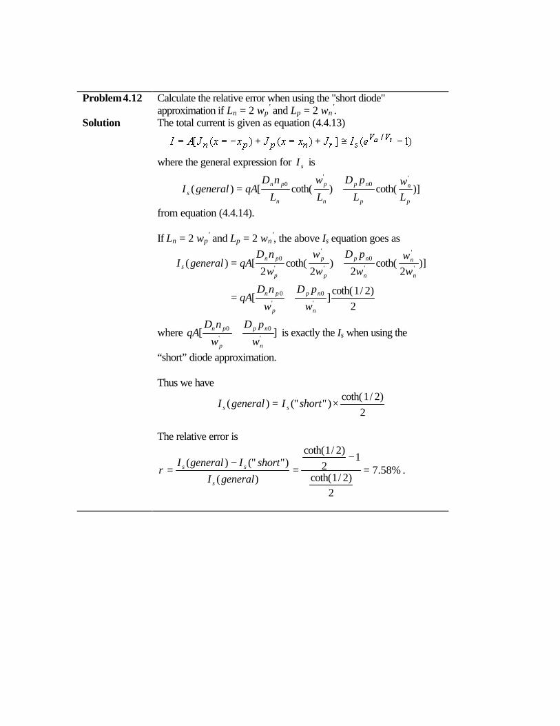
Problem 4.12 Calculate the relative error when using the "short diode"
approximation if Ln = 2 wp' and Lp = 2 wn
'. Solution The total current is given as equation (4.4.13)
where the general expression for sI is
)]coth()coth([)('
0'
0
p
n
p
np
n
p
n
pns L
wL
pD
L
w
L
nDqAgeneralI +=
from equation (4.4.14). If Ln = 2 wp
' and Lp = 2 wn', the above Is equation goes as
)]2
coth(2
)2
coth(2
[)( '
'
'0
'
'
'0
n
n
n
np
p
p
p
pns w
ww
pD
w
w
w
nDqAgeneralI +=
2
)2/1coth(][
'0
'0
n
np
p
pn
w
pD
w
nDqA +=
where ]['
0'
0
n
np
p
pn
w
pD
w
nDqA + is exactly the Is when using the
“short” diode approximation. Thus we have
2)2/1coth(
)"(")( ×= shortIgeneralI ss
The relative error is
%58.7
2)2/1coth(
12
)2/1coth(
)()"(")(
=−
=−
=generalI
shortIgeneralIr
s
ss .

Problem 4.13 A silicon p-n junction (Na = 1015 cm-3, wp = 1 µm and Nd = 4 x
1016 cm-3, wn = 1 µm) is biased with Va = 0.5 V. Use µn = 1000 cm2/V-s and µp = 300 cm2/V-s. The minority carrier lifetime is 10 µs and the diode area is 100 µm by 100 µm. a) Calculate the built-in potential of the diode. b) Calculate the depletion layer widths, xn and xp, and the
widths of the quasi-neutral regions. c) Compare the width of the quasi-neutral regions with the
minority-carrier diffusion-lengths and decide whether to use the "long" or "short" diode approximation. Calculate the current through the diode.
Compare the result of part c) with the current obtained by using the general solution (equation 4.4.14)
Solution a. The built-in potential is calculated from
2lni
adti n
NNV=φ = 0.69 V
b. The depletion layer width equals
))(11
(2
aida
s VNNq
w −+= φε
= 0.507 µm
from which the individual depletion layer width are obtained:
da
an NN
Nwx
+= = 0.012 µm
and
da
dp NN
Nwx
+= = 0.5 µm
The quasi-neutral region width are then: wn' = wn - xn = 0.99 µm wp' = wp - xp = 0.51 µm
c. The diffusion lengths are
nntn VL τµ= = 161 µm
pptnp VL τµ= = 88 µm
Since the diffusion lengths are larger than the corresponding quasi-neutral region widths, Ln >> wp' and Lp >> wn', we choose the "short" diode expression for the current:
)1e]([ /'
0'
0 −+= ta VV
n
np
p
pn
w
pD
w
nDAqI = 0.21 mA
d. The general expression,

)1e)](coth()coth([ /'
0'
0 −+= ta VV
p
n
p
np
n
p
n
pn
Lw
L
pD
L
w
L
nDAqI
yields the same result. e. The ratio of the electron current relative to the hole current
equals:
0
'
'0
np
n
p
pn
p
n
pDw
w
nD
II
= = 0.996
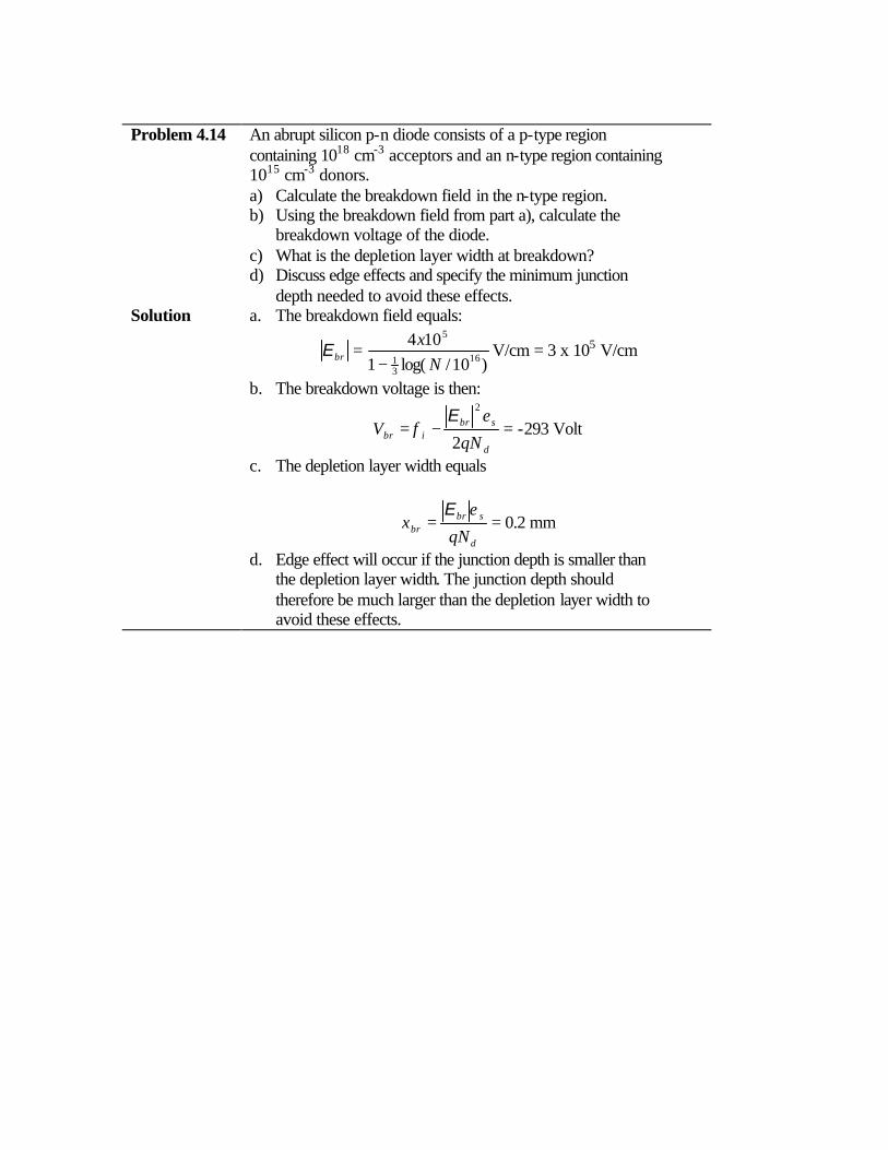
Problem 4.14 An abrupt silicon p-n diode consists of a p-type region
containing 1018 cm-3 acceptors and an n-type region containing 1015 cm-3 donors. a) Calculate the breakdown field in the n-type region. b) Using the breakdown field from part a), calculate the
breakdown voltage of the diode. c) What is the depletion layer width at breakdown? d) Discuss edge effects and specify the minimum junction
depth needed to avoid these effects. Solution a. The breakdown field equals:
)10/log(1104
1631
5
Nx
br −=E V/cm = 3 x 10⁵ V/cm
b. The breakdown voltage is then:
d
sbribr qN
V2
2ε
φE
−= = -293 Volt
c. The depletion layer width equals
d
sbrbr qN
xεE
= = 0.2 mm
d. Edge effect will occur if the junction depth is smaller than the depletion layer width. The junction depth should therefore be much larger than the depletion layer width to avoid these effects.

Problem 4.15 A 1 cm2 solar cell consists of a p-type region containing 1018 cm-
3 acceptors and an n-type region containing 1015 cm-3 donors. wp'
= 0.1 µm and wn’ >> Lp. Use µn = 1000 cm2/V-s and µp = 300
cm2/V-s. The minority carrier lifetime is 10 µs. The diode is illuminated with sunlight, yielding a photocurrent density of 30 mA/cm2.
a. Calculate the open circuit voltage and short-circuit current of the solar cell.
b. Calculate the maximum power generated by the call and the corresponding voltage and current.
c. Calculate the fill factor of the solar cell. d. Calculate the fill factor for the same cell when it is
illuminated by a concentrator so that the photocurrent density equals 300 A/cm2.

Solution The saturation current of the solar cell is calculated from:
][ 0'
0
p
np
p
pns L
pD
w
nDAqI +=
with Dn = µn Vt = 1000 x 0.0258 = 25.8 cm2/V-s DP = µP Vt = 300 x 0.0258 = 7.75 cm2/V-s
np0 = ni2/Na = 1020/1018 = 102 cm-3
pn0 = ni2/Nd = 1020/1016 = 104 cm-3
=×== −51075.7ppp DL τ 88 µm
yielding Is = 55.5 pA The maximum power is generated for:
tmtm VVs
t
mph
VVs
a
IVV
IIdVdP // e)1e(0 +−−==
where the voltage, Vm, is the voltage corresponding to the maximum power point. This voltage is obtained by solving the following transcendental equation:
tm
sphtm VV
IIVV
/1
/1ln
+
+=
Using iteration and a starting value of 0.5 V one obtains the following successive values for Vm:
Vm = 0.5, 0.442, 0.445 V The diode current Im equals and the power Pm generated equals:
Pm = Im x Vm = 12.6 mW The fill factor equals:
% 9.80030.052.00284.0445.0
factor fill =××
==scoc
mm
IVIV
Repeating for Iph = 300 A yields:
% 5.85300758.0289673.0
factor fill =××
==scoc
mm
IVIV

Problem 4.16 A semiconductor device made of silicon has, under thermal
equilibrium, an M-shaped electric field distribution as shown in the figure below.
MAX
1
0.5
0 a/2
x
a-a -a/2
a) Find Nd - Na between x = -a and x = a, as a function of Emax
b) Find the total potential across the semiconductor as a function of Emax with a = 0.1 µm
c) Find Emax and the built-in voltage φi d) Plot Nd - Na for -a ≤ x ≤ a and indicate numeric
values. Specify whether the different regions are p or n-type.

Solution a) From poisson’s one dimension equation:
s
ad
s
NNqdxd
εερε )( −
≅=
From the diagram above, for 2a
xa −≤≤− , a
ax max2)(
εε += ,
then Nd - Na = qas max2 εε
. Similarly, 02
≤≤− xa
, Nd - Na =
qas maxεε−
; 2
0a
x ≤≤ , Nd - Na = ;max
qasεε
and axa
≤≤2
, Nd - Na
= qa
s max2 εε−.
b) ∫ −= dxxx )()( εφ , )(xφ is the negative total area under )(xε .
So 4
5)(0 maxε
φφa
xtotal =−= . For a=0.1um, 4
105 max5ε
φ−×
=total
c) dti
dati NV
nNN
V ln2ln 2 ==φ4
5 maxεa= and
s
daqNε
ε2max = , then
we get =maxε 0.661*105, =iφ 0.83 V, Nd - Na = 0.87*1017, -
0.435*1017, 0.435*1017, -0.87*1017 cm-3 for 2a
xa −≤≤− ,
02
≤≤− xa
, 2
0a
x ≤≤ , and axa
≤≤2
.

Problem 4.17 Design an abrupt silicon p-n diode with a capacitance per unit
area of 10 nF/cm2 in thermal equilibrium and a maximum electric field of 50 kV/cm at a reverse bias of 10 Volt. Provide values of the acceptor and donor density, the built-in potential and the depletion layer width in thermal equilibrium and at a reverse bias of 10 Volt.
Solution The capacitance per unit area at thermal equilibrium is
d
sj x
Cε
=
where we can derive cmxd410054.1 −×= .
The xd at thermal equilibrium is also given as
ida
dasd NN
NNq
x φε +
=2
.
The maximum electric field under applied voltage Va is
)(2
)(2
max
aida
da
s
aida
das
da
a
s
d
dda
a
s
d
s
nd
VNN
NNq
VNNNN
qNNNqN
xNN
NqNxqNE
−+
=
−+
+=
+==
φε
φε
ε
εε
So multiply Emax and xd, we have 27.52max =×−×=× iaid VxE φφ , where 10−=aV V.
We can solve the above equation and get 651.0=iφ V. From the above xd equation and the built-in potential equation
)ln(2i
dati n
NNV=φ , we finally have
1510993.9 ×=aN 3−cm , 1410376.8 ×=dN 3−cm , or 1510993.9 ×=dN 3−cm , 1410376.8 ×=aN 3−cm .
And the depletion layer width at thermal equilibrium is
cmxd410054.1 −×= , and at a reversed-biased 10V is
cmxd410261.4 −×= .

Problem 4.18 A silicon p-n junction consists of a half-sphere with one-micron
radius and a doping density of 1018 cm-3 embedded in an n-type substrate with a donor density of 1016 cm-3. Breakdown occurs in the diode when the maximum field reaches 6x10⁵ V/cm. Calculate the breakdown voltage. Justify any assumptions you make.
Solution Assuming a one-sided, abrupt junction, full ionization and using the full depletion approximation, the charge density equals:
0)( =rρ , for r < r0
dqNr =)(ρ , for r0 < r < r1 0)( =rρ , for r1 < r
The corresponding electric field equals 0)( =rE , for r < r0
s
d
rrrqN
rε2
31
3
3)(
)(−
=Ε , for r0 < r < r1
0)( =rE , for r1 < r So for maximum E(r), we have r = r0. Then
s
d
rrrqN
rε2
31
3
3)(
)(−
=Ε =-6*105. So r1 = 2.343um.
The total voltage equals ∫−=1
0
)(r
ria drrV Eφ = 15.43 V, here
2lni
dati n
NNV=φ = 0.834 V.

Problem 4.19 Calculate the built-in voltage for a silicon p-n junction with Na =
Nd = 1015 cm-3 at T = 500 K. Do not assume the electron and hole concentration to equal the donor or acceptor concentration.
Solution The intrinsic carrier density at T=500K can be calculated and find from Example 2.4.6 or Figure 2.6.3, as
3141016.2)500( −×= cmKn i . Assume shallow donors and acceptors, where dd NN ≅+ , and
aa NN ≅− . In n-type region ( 0==−
aa NN , 31510 −+ =≅ cmNN dd ), we can
applied equation 2.6.34 to calculated the 0nn and 0np by
315220 10045.1)
2(
2−
−+−+
×=+−
+−
= cmnNNNN
n iadad
n
and for non-degenerate 3130
20 10466.4/ −×== cmnnp nin .
In p-type region ( 0==+
dd NN , 31510 −− =≅ cmNN aa ), we can applied equation 2.6.35 to calculated the 0nn and 0np by
315220 10045.1)
2(
2−
+−+−
×=+−
+−
= cmnNNNN
p idada
p
and for non-degenerate 3130
20 10466.4/ −×== cmpnn pip .
Thus the built-in voltage iφ is
136.0ln2
00 ==i
pnti n
pnVφ V.

Problem 4.20 Derive the minority electron density in a silicon p-n junction at
the edge of the depletion region as a function of the acceptor density and the applied voltage. State the approximations made. Calculate the minority carrier density for Na = 1017 cm-3, Nd = 1016 cm-3 and Va = -2 V.
Solution In the deplete region without Va, 2ln
i
dati n
NNV=φ , and dn Nn ≅0 ,
a
ip N
nn
2
0 = . So 0
0lnp
nti n
nV=φ , or t
i
Vnp enn
φ−
= 00 . Here we assume
full depletion and shallow dopant.
With applied voltage, 0
0lnp
ntai n
nVV =−φ , then
t
a
t
a
VV
a
iVV
pp eNn
enn2
0 == .
For Na =1017 cm-3, Nd =1016 cm-3, and Va = -2 V, get np = 2.58 x 10⁻³¹ cm-3.

Problem 5.1 A silicon npn bipolar transistor with NE = 1018 cm-3, NB = 1017
cm-3 and NC = 1016 cm-3, wE = 1 µm, wB = 0.5 µm , and wC = 4 µm is biased with VBE = 0.6 V and VCB = 0 V. Use µn = 1000 cm2/V-s, µp = 300 cm2/V-s and τn = τp = 100 ns. The emitter area equals 10-4 cm2. a) Calculate the width of the quasi-neutral regions in the
emitter, base and collector. b) Calculate the minority-carrier diffusion lengths in the
emitter, base and collector. Calculate the ratio of the minority-carrier diffusion length and the quasi-neutral region width in each region.
c) Calculate the excess-minority-carrier charge density per unit area in the emitter, base and collector.
d) Calculate the emitter current while ignoring the recombination in the depletion region.
e) Calculate the base transit time and the current due to recombination of electrons in the base.
f) Calculate the emitter efficiency and the base transport factor. g) Calculate the transport factor and the current gain assuming
there is no recombination in the depletion regions. h) Calculate the collector capacitance, the majority-carrier
charge density in the base and the Early voltage.

Solution BEnEE xww ,
' −=
BCpBEpBB xxww ,,' −−=
BCnCC xww ,' −=
+
−=
EBE
BBEBEisBEn NNN
Nq
Vx
1)(2 ,,
φε
+
−=
EBB
EBEBEisBEp NNN
Nq
Vx
1)(2 ,,
φε
+
−=
CBB
CBCBCisBCp NNN
Nq
Vx
1)(2 ,,
φε
+
−=
CBC
BBCBCisBCn NNN
Nq
Vx
1)(2 ,,
φε
nnn DL τ= = 16.1 µm nnn DL τ= = 16.1 µm nnn DL τ= = 16.1 µm
21)exp(
'2
,B
t
BE
B
iEBn
wV
VNn
AqQ
−=∆
−
= 1)exp(
',2
,t
BE
BB
BnEinE V
V
wN
DAqnI
−
= 1)exp(
',2
,t
BE
EE
EpEipE V
V
wN
DAqnI
Bn
Br D
wt
,
2'
2=
n
BnBr
QI
τ,
,∆
=
',
',
1
1
EEBn
BBEpE
wND
wND+
=γ
nBn
B
n
rT D
wtττ
α,
2'
211 −=−=
rET δγαα =
αα
β−
==1B
CII
'
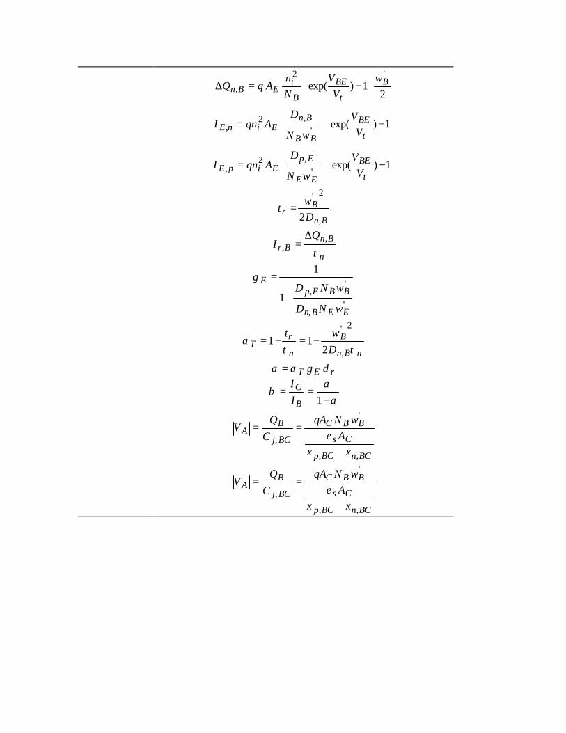
21)exp(
'2
,B
t
BE
B
iEBn
wV
VNn
AqQ
−=∆
−
= 1)exp(
',2
,t
BE
BB
BnEinE V
V
wN
DAqnI
−
= 1)exp(
',2
,t
BE
EE
EpEipE V
V
wN
DAqnI
Bn
Br D
wt
,
2'
2=
n
BnBr
QI
τ,
,∆
=
',
',
1
1
EEBn
BBEpE
wND
wND+
=γ
nBn
B
n
rT D
wtττ
α,
2'
211 −=−=
rET δγαα =
αα
β−
==1B
CII
BCnBCp
Cs
BBC
BCj
BA
xxA
wNqAC
QV
,,
'
,+
==ε
BCnBCp
Cs
BBC
BCj
BA
xxA
wNqAC
QV
,,
'
,+
==ε

Problem 5.2 A silicon npn bipolar transistor has an emitter doping, NE = 2 x
1018 cm-3, an emitter width wE’ = 1 µm, and a base doping of 2 x
1017 cm-3. A current gain of 100 and an Early voltage of 100 V is desired. Using µn = 1000 cm2/V-s, µp = 300 cm2/V-s and τn = τp = 100 ns, find the corresponding quasi-neutral base width and collector doping. The emitter area equals 10-4 cm2.
Solution The quasi-neutral width of the base, wB’, can be obtained from
the current gain, β , which is given by:
EBBEp
EEBn
wND
wNDγαβ ≅≅ if ,
',
',
Yielding wB’ = 0.335 µm Note that this implies that the base transport factor, aT, is very close to one and therefore that the diffusion length of electrons in the base must be much larger than the base width. The diffusion length equals:
nnn DL τ= = 16.1 µm which is indeed much larger than the quasi-neutral base width The collector doping density is obtained from the Early voltage:
BCnBCp
s
BB
BCj
BA
xx
wqNCQ
V
,,
'
,
+
==ε
This equation allows to find first the width of the depletion region between the base and collector, namely:
xp,BC + xn,BC = xd,BC = 0.987 µm And can then be used to find the doping density using
+
−==+
CB
BCisBCdBCnBCp NNq
Vxxx
11)(2,,,
φε
The resulting collector doping density equals 9.69 x 1014 cm-3.

Problem 6.1 Consider an aluminum-SiO2-silicon MOS capacitor (ΦM = 4.1 V, εox/ε0 = 3.9, χ = 4.05 V and Na = 1017 cm-3) MOS capacitor with tox = 5 nm. a) Calculate the flatband voltage and threshold voltage. b) Repeat for an n-type silicon substrate with Nd = 1016 cm-3. c) Repeat with a surface charge of 10-7 C/cm2
. d) Repeat with a charge density in the oxide of 10-1 C/cm3 .

Solution The work function difference of the nMOS capacitor equals
)ln(2 i
at
gMSM n
NV
q
E−−−Φ=Φ−Φ χ
= 4.1 - 4.05 - 0.56 - 0.42 = -0.93 = VFB Since no charge is present in the oxide or at the interface, the flat band voltage equals the work function difference. The threshold voltage equals:
V 15.0 105/1085.89.3
42.010106.11085.89.114
42.0293.0
42
714
171914
=×××
×××××××+
×+−=
++=
−−
−−
ox
FasFFBT C
qNVV
φεφ
For the pMOS capacitor one finds similarly:
)ln(2 i
dt
gMSM n
NV
q
E+−−Φ=Φ−Φ χ
= 4.1 - 4.05 -0.56 + 0.36 = - 0.15 = VFB and
V 94.0 105/1085.89.3
36.010106.11085.89.114
36.0215.0
42
714
161914
−=×××
×××××××−
×−−=
−−=
−−
−−
ox
FdsFFBT C
qNVV
φεφ
In the presence of 10-7 C/cm2 interface charge the flat band voltage of the nMOS capacitor becomes:
ox
iMSFB C
QV −Φ= = - 0.93 - 0.145 = - 1.07
The threshold voltage shift by the same amount yielding: VT = 0.15 - 0.145 = - 0.005
In the presence of 10-1 C/cm3 throughout the oxide the flat band voltage of the nMOS capacitor becomes:
∫−Φ=oxt
oxox
MSFB dxxxV0
)(1
ρε
= - 0.93 - 0.03 = - 0.96
The threshold voltage shift by the same amount yielding: VT = 0.149 - 0.036 = 0.113 V

Problem 6.2 A high-frequency capacitance voltage measurement of a silicon
MOS structure was fitted by the following expression: C(VG) = 6 pF + 12 pF/(1 + exp(VG))
a) Calculate the oxide capacitance per unit area and the oxide thickness. The area of the capacitor is 100 x 100 micron and the relative dielectric constant equals 3.9.
b) From the minimum capacitance, calculate the maximum depletion layer width and the substrate doping density.
c) Calculate the bulk potential. d) Calculate the flatband capacitance and the flatband voltage. e) Calculate the threshold voltage

Solution (a) The oxide capacitance is when −∞∝GV , and from above equation, we have C(VG) = 18 pF, so
Cox = 84
12
101810
1018 −−
−
×=×
F/cm2 = 180 nF/cm2.
The oxide thickness is
2.1910180
10854.89.39
14
=×
××==
−
−
ox
oxox C
tε
µm.
(b) The minimum capacitance is C(VG) = 6 pF when ∞∝GV ,
Cmin = 84
12
10610106 −
−
−
×=×
F/cm2 = 60 nF/cm2.
Since Cmin =
s
d
ox
xC ε
max11
+, we can derive xd,max = 117 nm.
From a
Fsd qN
x)2(2 φε
= , and i
atF n
NV ln=φ , Na can be
calculated by iteration as Na = 7.8 x 1016 cm-3. (c) The bulk potential 411.0)/ln( == iatF nNVφ V. (d) For the capacitance under flat band voltage,
4.141044.1101
1 74 =××=+
⋅= −−
s
D
ox
FB LC
AC
ε
pF
where LD is the Debye length given as:
a
tsD qN
VL
ε= = 1.478 x 10⁻⁶ cm.
Plug CFB in the expression of the capacitance, we have the Flat band voltage VFB as:
6=FBC pF + 12 pF/(1+exp(VFB)) where VFB = - 0.847 V. (e) The threshold voltage VT is equal to
817.02411.0847.04
2 +×+−=++=ox
FasFFBT C
qNVV
φεφ =
0.792 V.

Problem 6.3 An MOS capacitor with an oxide thickness of 20 nm has an
oxide capacitance which is three times larger than the minimum high-frequency capacitance in inversion. Find the substrate doping density.
Solution The high frequency capacitance in inversion equals:
s
Td
ox
invHFox x
C
CC
ε,
, 13
3+
==
from which one finds xd,T = 2 εs/Cox so that:
2ox
s
Fa C
qN
εφ
=
where the bulk potential, φF, also depends on the doping density, Na
Iterating, starting with φF = 0.4, yields the following values for the doping density:
Na = 7.06 x 10¹⁶, 7.20 x 10¹⁶ and 7.21 x 1016 cm-3
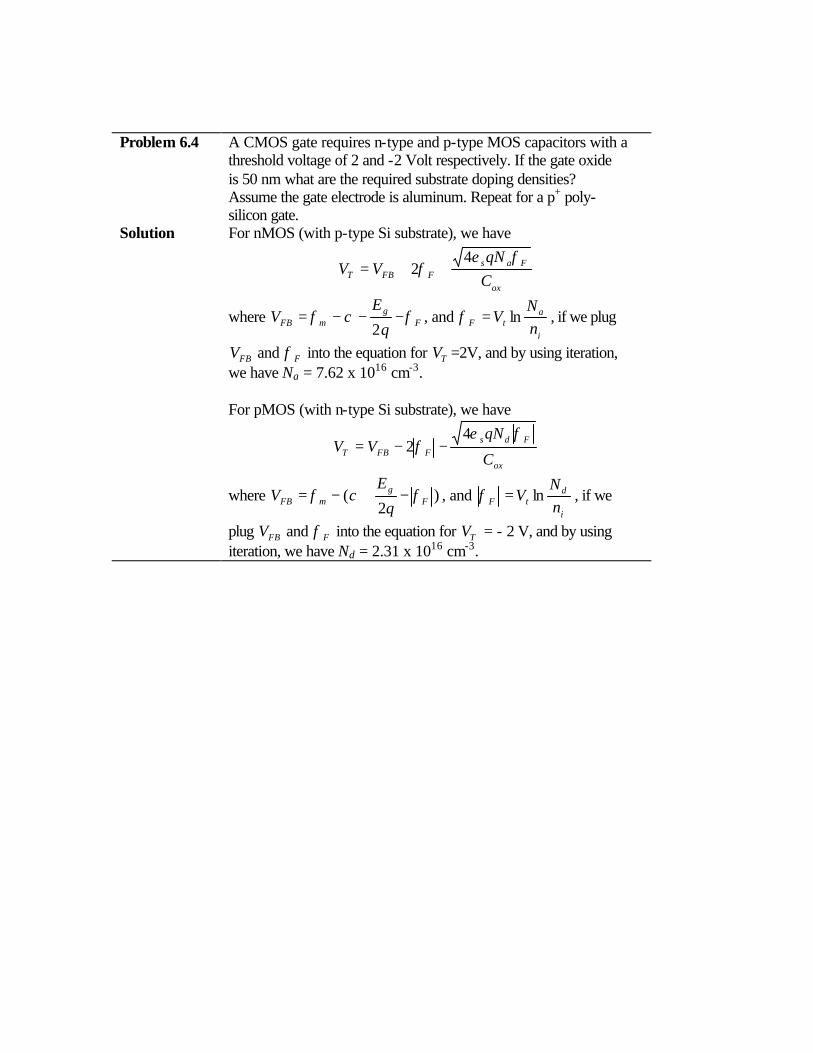
Problem 6.4 A CMOS gate requires n-type and p-type MOS capacitors with a
threshold voltage of 2 and -2 Volt respectively. If the gate oxide is 50 nm what are the required substrate doping densities? Assume the gate electrode is aluminum. Repeat for a p+ poly-silicon gate.
Solution For nMOS (with p-type Si substrate), we have
ox
FasFFBT C
qNVV
φεφ
42 ++=
where Fg
mFB q
EV φχφ −−−=
2, and
i
atF n
NV ln=φ , if we plug
FBV and Fφ into the equation for TV =2V, and by using iteration, we have Na = 7.62 x 1016 cm-3. For pMOS (with n-type Si substrate), we have
ox
FdsFFBT C
qNVV
φεφ
42 −−=
where )2
( Fg
mFB q
EV φχφ −+−= , and
i
dtF n
NV ln=φ , if we
plug FBV and Fφ into the equation for TV = - 2 V, and by using iteration, we have Nd = 2.31 x 1016 cm-3.

Problem 6.5 Consider a p-MOS capacitor (with an n-type substrate) and with
an aluminum gate. Find the doping density for which the threshold voltage is 3 times larger than the flat band voltage. tox = 25 nm. Repeat for a capacitor with 1011 cm-2 electronic charges at the oxide-semiconductor interface.
Solution a) For p-MOS flat band voltage
FBox
FdsFFBT V
CqN
VV 34
2 =−−=φε
φ
And flat band voltage equals
)ln(2 i
dt
gMFB n
NV
q
EV +−−Φ= χ
So, one gets
02.14
4 =+ox
FdsF C
qN φεφ
Here, )ln(i
dtF n
NV=φ . By using iteration way, one finds Nd =
1.38 x 1014 cm-3. b) Repeat with Qi = 10 –7, one has
ox
iMSFB C
QV −Φ=
Similarly using iteration, one obtains Nd = 5.3 x 1016 cm-3.

Problem 6.6 A silicon p-MOS capacitor. (Nd = 4 x 1016 cm-3, tox = 40 nm) is
biased halfway between the flatband and threshold voltage. Calculate the applied voltage and the corresponding capacitance
Solution For the bias halfway between the flatband and threshold voltage,
2TFB
G
VVV
+=
ox
FdsFFB C
qNV
φεφ −−= (1),
where ox
FdsFFBT C
qNVV
φεφ
42 −−= .
VG also equals to
ox
sdssFBG C
qNVV
φεφ
2−−= (2).
We can equal (1) and (2), and get
ox
FdsF C
qN φεφ + =
ox
sdss C
qN φεφ
2+ (3),
where i
dtF n
NV ln=φ . From Nd = 4 x 1016 cm-3 we can get
394.0=Fφ V, and substitute Fφ in equation (1) and (3) we have 11.1−=GV V and 28.0=sφ V, where
)2
( Fg
mFB q
EV φχφ −+−= .
From sφ we can calculate a
ssd qN
xφε2
= = 9.6 x 10⁻⁶ cm, and the
total capacitance C =
s
d
ox
xC ε
+1
1 =
s
d
ox
ox xtεε
+
1 = 48.2 nF/cm2.
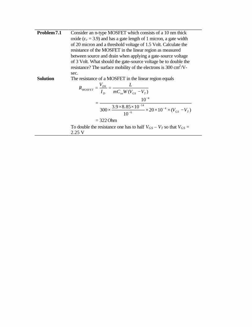
Problem 7.1 Consider an n-type MOSFET which consists of a 10 nm thick oxide (εr = 3.9) and has a gate length of 1 micron, a gate width of 20 micron and a threshold voltage of 1.5 Volt. Calculate the resistance of the MOSFET in the linear region as measured between source and drain when applying a gate-source voltage of 3 Volt. What should the gate-source voltage be to double the resistance? The surface mobility of the electrons is 300 cm2/V-sec.
Solution The resistance of a MOSFET in the linear region equals
Ohm322
)(102010
1085.89.3300
10
)(
46
14
4
=
−×××××
×=
−==
−−
−
−
TGS
TGSoxD
DSMOSFET
VV
VVWCL
IV
Rµ
To double the resistance one has to half VGS – VT so that VGS = 2.25 V

Problem 7.2 Consider an n-type MOSFET with an oxide thickness tox = 20
nm (εr = 3.9) and a gate length, L = 1 micron, a gate width, W = 10 micron and a threshold voltage, VT = 1 Volt. Calculate the capacitance per unit area of the oxide, COX, and from it the capacitance of the gate, CG. Calculate the drain current, ID, at a gate-source voltage, VGS = 3 Volt and a drain-source voltage, VDS = 0.05 Volt. The surface mobility of the electrons µn = 300 cm2/V-sec. Use the linear model of the MOSFET.
Solution For n-type MOSFET, capacitance per unit area of the oxide is 71073.1 −×==
ox
oxox t
Cε
F/cm2.
And the capacitance of the gate is oxoxG LWCACC == = 17.3 fF.
Drain current ID is given by
9.1.5)( =−= DSTGSoxnD VVVL
WCI µ uA.

Problem 7.3 A n-type MOSFET (L = 1 µm, tox = 15 nm, VT = 1 V and µn =
300 cm2/V-sec) must provide a current of 20 mA at a drain-source voltage of 0.5 Volt and a gate-source voltage of 5 Volt. How wide should the gate be?
Solution The MOSFET is not in saturation so that the gate width can be obtained from:
micron154
5.0)25.015(105.1
1085.89.3300
1002.0
)2
(
6
14
4
=
×−−××
×××
×=
−−=
−
−
−
x
VV
VVC
LIW
DSDS
TGSox
D
µ

Problem 7.4 A MOSFET (L = 1 µm, tox = 10 nm, VT = 1 V and µn = 300
cm2/V-sec) is to be used as 50 Ω terminating resistor when applying a gate-source voltage, VGS = 5 Volt. How wide should the gate be?
Solution The linear model applies to linear devices (resistors) case here. One finds drain current
RV
VVVLW
CI DSDSTGSoxnD =−= )(µ
Then, the gate width can be found, yielding W = 48 um.

Problem 7.5 The capacitance of an n-type silicon MOSFET is 1 pF. Provided
that the oxide thickness is 50 nm and the gatelength is 1 micron, what is the resistance of the MOSFET in the linear regime when biased at a gate voltage, which is 5 Volt larger than the threshold voltage? Use a reasonable value for the surface mobility knowing that the bulk mobility equals 1400 cm2/V-sec.
Solution The width of the gate is obtained from WLCC oxG = So that the width equals:
mm45.110
1051085.89.3
10
46
14
12
=×
×××
==−
−
−
−
LCC
Wox
G
The resistance of the MOSFET then equals:
Ohm5
5145.0105
1085.89.3400
10
)(
6
14
4
=
×××
×××
=
−==
−
−
−
TGSoxD
DSMOSFET VVWC
LI
VR
µ
The mobility was chosen to be 400 cm2/V-s, which is about half the mobility in bulk material doped with 1017 cm-3 acceptors.

Problem 7.6 Consider a p-channel silicon MOSFET with an aluminum gate.
a) Draw the energy band diagram of the MOS structure for VG = VFB. Indicate the workfunction of the metal and the semiconductor, as well as the electron affinity.
b) Draw the field distribution for VG = VT (onset of inversion).
c) Calculate the depletion layer width and the field in the oxide at the onset of inversion. (Nd = 1016 cm-3, tox = 100 nm, VFB = -0.5V)
Solution c) The depletion layer width equals
307.04
, ==d
FsTd qN
xφε
µm.
At the onset of inversion, Qinv = 0, so that the total charge per unit area equals:
Tddd xqNQ ,= = εsEs = εoxEox So that:
Eox = 5104.1 ×=ox
dQε
V/cm.
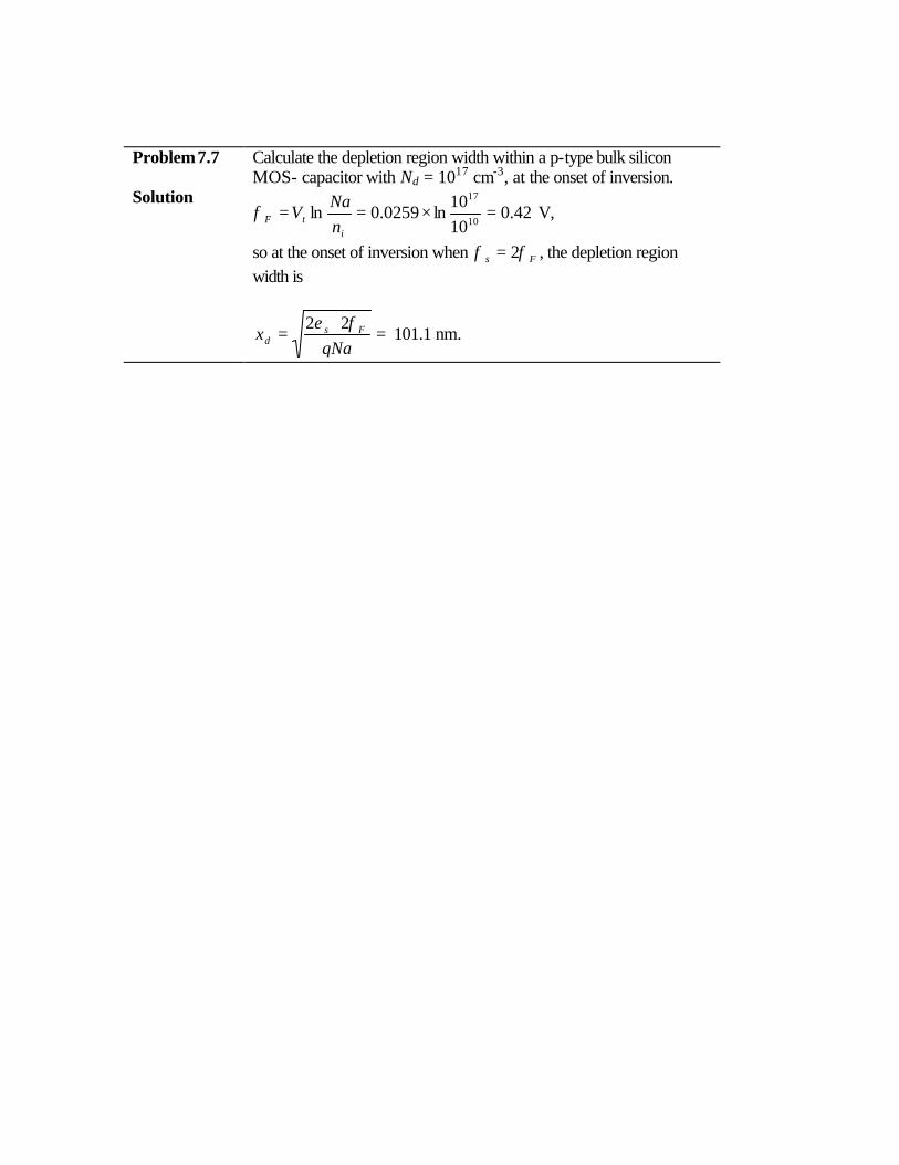
Problem 7.7 Calculate the depletion region width within a p-type bulk silicon
MOS- capacitor with Nd = 1017 cm-3, at the onset of inversion. Solution
42.01010
ln0259.0ln10
17
=×==i
tF nNa
Vφ V,
so at the onset of inversion when Fs φφ 2= , the depletion region width is
=⋅
=qNa
x Fsd
φε 22 101.1 nm.

7.8. Power MOSFETs
7.8.1. LDMOS
The Laterally Diffused MOSFET (LDMOS) is an asymmetric power MOSFET designed for low on-resistance and high blocking voltage. These features are obtained by creating a diffused p-type channel region in a low-doped n-type drain region. The low doping on the drain side results in a large depletion layer with high blocking voltage. The channel region diffusion can be defined with the same mask as the source region, resulting in a short channel with high current handling capability. The relatively deep p-type diffusion causes a large radius of curvature at the edges, which eliminates the edge effects discussed in section 4.5.2. While the device’s name implies that the fabrication require a diffusion, the dopants can just as well be implanted and annealed. Diffusion can be used in addition to further increase the junction depth and radius of curvature.
A typical structure is presented in Figure 7.8.1. The device can be fabricated by diffusion as well as ion implantation. The p-type region is formed first, followed by shallow p+ and n+ regions. The n+ regions provide both source and drain contact regions. The p+-region contacts the p-type body, which is typically shorted to the source, thereby eliminating the body effect.
Figure 7.8.1. Cross-section of a Laterally Diffused MOSFET (LDMOS) structure.
The LDMOS structure combines a short channel length with high breakdown voltage as desired for high power RF amplifiers in numerous applications. This device is currently the device of choice for RF power amplifiers in base stations of wireless communications systems as well as numerous UHF and L-band power amplifiers in broadcast, communication and radar systems.
7.8.2. VMOS Transistors and UMOS
The VMOS transistor named after the V-shaped groove, is a vertical MOSFET with high current handling capability as well as high blocking voltage. It consists of a double diffused n+/p layer, which is cut by a V-shaped groove as shown in Figure 7.8.2.a. The V-groove is easily fabricated by anisotropically etching a (100) silicon surface using a concentrated KOH solution. The V-
p+ substrate
Bulk
p
Gate
p-
n+
n
Source Drain
p+ n+
p+ substrate
Bulk
p
Gate
p-
n+
n
Source Drain
p+ n+

groove is then coated with a gate oxide, followed by the gate electrode. As the V-groove cuts through the double diffused layer, it creates two vertical MOSFETs, one on each side of the groove. The combination of the V-groove with the double diffused layers results in a short gatelength, which is determined by the thickness of the p-type layer. The vertical structure allows the use of a low-doped drain region, which results in a high blocking voltage.
Figure 7.8.2. Cross-section of two vertical MOSFET structures: a) VMOS and b) UMOS.
Another alternate structure is the UMOS structure. A vertical trench is etched though the double diffused layer, again resulting in two vertical MOSFETs.
Either one of these vertical structures can further be combined with the HEXFET layout. This layout resembles a honeycomb structure in which the hexagonal areas are source areas, while the gate metal is located on the perimeters.
7.8.3. Insulated Gate Bipolar Transistors (IGBTs)
The Insulated Gate Bipolar Transistor or IGBT for short combines the high DC current gain of a MOSFET with the high current handling capability and high blocking voltage of a BJT in a surprisingly simple structure such as the one shown in Figure 7.8.3. At first glance the vertical structure looks like that of a regular bipolar transistor structure. However a closer look reveals a p+ substrate rather than an n+ substrate. To further analyze this structure we use the equivalent circuit, which contains the p-n-p BJT as formed by the bottom three layers as well as the n-MOSFET underneath the gate electrode. One should note that the p-type collector of the p-n-p BJT and the n-type source of the n-MOSFET share the same metal contact. Also, that the drain region of the n-MOSFET is the buried n-type layer, which is the n-type base of the p-n-p BJT. The electrons originating from the n+ source flow laterally underneath the gate and then flow down in the buried n-type region, thereby supplying the gate current of the p-n-p BJT. Since the gate current is provided locally, the emitter current will be concentrated around the same area. Note that under typical operation the collector would be grounded while the positive voltage is applied to the emitter. Therefore this device can be connected in a switching circuit just like an n-p-n BJT with the important distinction that no gate current is required to maintain the on-state current.
n+ substrate
Drain
pn+
GateSource
n-
n+ substrate
Drain
pn+
GateSource
n-
Drain
p n+
GateSource
Drain
p n+
GateSource
n-
n+ substrate
Drain
p n+
GateSource
Drain
p n+
GateSource
n-
n+ substrate

Figure 7.8.3 Insulated Gate Bipolar Transistor (IGBT): a) equivalent circuit and b) device cross-section.
p substrate
Collector/Source
n
n+
Gate Collector/Source
n+p
Emitter (+V)
p
Emitter
Collector
Gate
Collector
p substrate
Collector/Source
n
n+
Gate Collector/Source
n+p
Emitter (+V)
p
Emitter
Collector
Gate
Collector

Problem 7.9 A silicon MOSFET (ni = 1010 cm-3, εs/ε0 = 11.9 and εox/ε0 = 3.9)
is scaled by reducing all dimensions by a factor of 2 and by increasing the doping density of the substrate by a factor of 4. Calculate the ratio of the following parameters of the scaled device relative to that of the original device: (make approximations if necessary) (a) The transconductance at VGS - VT = 1 V. (b) The gate capacitance (c) The transit frequency at VGS - VT = 1 V. (Assume that CDS = 0) (d) The threshold shift when increasing the reverse bias of the source-bulk diode from 1 Volt to 3 Volt. (e) The breakdown voltage of the oxide assuming the breakdown field to be constant. (f) The breakdown voltage of the drain-to-bulk p-n diode assuming the breakdown field to be constant.
Solution (a) DSoxm V
Lw
Cg µ∝ , 0' 2 mm gg =
(b) ox
oxox
GS
invG t
CVQ
Cε
−=−=∂∂
= , 0' 2 GG CC ⋅=
(c) 22
1L
VLv
tf DS
rT µ
π∝∝= , 0' 4 TT ff =
(d) ox
asT C
qNV
εγ
2=∝∆ , 0'
TT VV ∆=∆
(e) oxoxbroxbr tV ×=,, E , 0
,'
, 5.0 oxbroxbr VV ⋅=
(f) dDBbrDBbr xV ×=,, E , where
s
daDB
xqNε
=E . When Na
increases 4 times, to keep DB
E constant, xd decreases by 4
times. So 0,
', 4
1DBbrDBbr VV = .

Problem 7.10 A silicon p-substrate (p ≅ Na = 1016 cm-3) MOSFET with tox =
0.1 µm, εox/ε0 = 3.9 and VFB = -0.2 V, has a threshold voltage which is 1 Volt smaller than desired. By what value should one change the oxide thickness, tox, to obtain the desired threshold voltage? Should one increase or decrease the oxide thickness?
Solution Similar to #7.8,
ox
FasFFBT C
qNVV
φεφ
42 ++=
and one has
14
=∆=∆ Toxox
Fas VtqNε
φε
Then oxt∆ = 0.07 µm, and 2,oxt should be increased to 0.17 µm or 170nm.

A10-1
A10. Appendix 10: Maxwell’s Equations A10.1. Maxwell’s differential equations for free space
ερ
=⋅∇ Err
(A10.1.1)
0=⋅∇ Brr
(A10.1.2)
tB
∂∂−=×∇
rrrE
(A10.1.3)
tcJB
∂∂+=×∇ E
rrr
201µ
(A10.1.4)
A10.2. Maxwell’s integral equations for free space
∫∫∫∫∫ =⋅VS
dVsd ρεrr
E0 (A10.2.1)
0=⋅∫∫S
sdBrr
(A10.2.2)
∫∫∫ ⋅−=⋅SL
sdBdtd
ldrrrr
E (A10.2.3)
∫∫∫∫∫ ⋅+⋅=⋅SSL
sddtd
sdJldB rrrrrr
E00
εκµ
(A10.2.4)

Appendix 5
Title Page Table of Contents Help Copyright B. Van Zeghbroeck, 2004
Appendix:
Appendix 11: Chemistry related issues
The mass action law
The term Mass Action law refers to the equilibrium condition for chemical reactions. It states that the product of the concentrations of the reacting molecules or ions divided by the product of the concentrations of the reaction products equals a constant. For a reaction of the form:
aA + bB ↔ cC
where A, B and C are the molecules or ions and a, b and c are the integers needed to match the stochiometry requirement. The equilibrium condition is then given by:
[A]a [B]b = k(T) [C]c
where the square brackets denote the concentrations of each molecule or ion.
This equation simply states that the probability of a reaction taking place is proportional to the probability that each of the reacting elements are available which in turn is proportional to the concentration. In the case where more than one molecule of the same type is needed the concentration of that molecule is multiplied with itself as many times as this molecule is needed in the reaction.
Similarly one calculates the probability that a reaction takes place in the reverse direction. In equilibrium the ratio of both probabilities is a constant, named k(T) where the temperature dependence is added explicitely to indicate that this constant depends (rather strongly) on temperature.
Example: dissociation of water
Applying the mass action law to the dissociation of water as described by the following chemical reaction:
H+ + OH- = H2O
one obtains:
[H+] [OH-] = kH2O [H2O]
Since the concentration of water is almost constant as the concentration of the ions is much smaller than the concentration of water molecules, this equation reduces at room temperature to:
http://ece-www.colorado.edu/~bart/book/book/append/append11.htm (1 of 2)11/10/2004 17:23:33

Appendix 5
[H+] [OH-] = 10-14 (moles/liter)2
pH of aqueous solutions
The pH of an aqauous solution is given by the logarithm of the hydroxyl ion concentration in units of moles/liter.
pH = -log10([H+])
To apply this equation to the dissociation of pure water one first has to find the concentration of the hydroxyl ions. Since a water molecule dissociates into one hydroxyl ion and one hydrogen ion the hydroxyl concentration equals the hydrogen concentration so that at room temperature both equal 10-7 moles/liter or 6.0 x 1013 cm-3 1. The pH of water at room temperature therefore equals 7.
resistivity of pure water
The conductivity of pure water is due to the motion of the hydroxyl and hydrogen ions, while the neutral water molecules do not contribute. At room temperature (25°C) the conductivity is 1/(18.3 MΩcm). Assuming that the hydrogen ions have a much higher mobility (due to their smaller size) one find the mobility to be 5.7 x 10⁻³ cm2/V-s.
Analogy between semiconductors and aqueous solution
Based on the review above one finds that electrons and holes in semiconductors have a lot in common with hydroxyl and hydrogen ions in aqueous solutions: just like electron-hole pairs are generated in intrinsic semiconductors, hydroxyl and hydrogen ions are created in equal quantities in pure water. Adding a base increases the hydroxyl concentration which then forces the hydrogen concentration to go down to satisfy the equlibrium condition. The pH increases logarithmically with the hydroxyl density. This is analogous to adding donors to an intrinsic semiconductor which adds electrons and reduces the hole density. The Fermi energy increases with the logarithm of the electron density. Adding an acid to an aqueous solution is analogous to adding acceptors to a semiconductor. This explains why the term mass-action law is used to describe the relation between the electron and hole densities in thermal equilibrium.
1 1 mole/liter contains 6.022 x 10²³ atoms/liter which corresponds to a density of 6.0 x 1020 cm-3
http://ece-www.colorado.edu/~bart/book/book/append/append11.htm (2 of 2)11/10/2004 17:23:33

A12-1
Appendix 12: Vector Calculus The del operator
zyx zyx ∂∂
+∂∂
+∂∂
=∇ eeerrr
(A12.1)
The divergence
zyxzyx
∂∂
+∂
∂+
∂∂
=∇EEEE
r
(A12.2)
The gradient
zyx zyx
eeerrrr
∂∂
+∂∂
+∂∂
=∇φφφ
φ (A12.3)
The Laplacian
2
2
2
2
2
22
zyx ∂
∂+
∂
∂+
∂
∂=∇
φφφφ
(A12.4)
The Laplacian in cylindrical coordinates
θcosrx = , θsinry = , zz =
2
2
2
2
22
2
2
22 11
zrrrr ∂Ψ∂
+∂
Ψ∂+
∂Ψ∂
+∂
Ψ∂=Ψ∇
θ
2
2
2
2
22 1
)(1
zrrr
rr ∂Ψ∂
+∂
Ψ∂+
∂Ψ∂
∂∂
=Ψ∇θ
(A12.6)
The Laplacian in spherical coordinates
φθ cossinrx = , φθ sinsinrx = , θcosrz =
2
2
22222
sin1
)(sinsin1
)(1
φθθθ
θθ ∂Ψ∂
+∂Ψ∂
∂∂
+∂Ψ∂
∂∂
=Ψ∇rrrrr
(A12.7)

A12-2
The vector product
zxy
yxz
xyz
zyx
zyx
yxzxzy
zyxx
e )(e )(e )(
eee
rrr
rrr
rr
∂∂
−∂
∂+
∂∂
−∂
∂+
∂
∂−
∂∂
=
∂∂
∂∂
∂∂
=∇
EEEEEE
EEE
E
(A12.5)
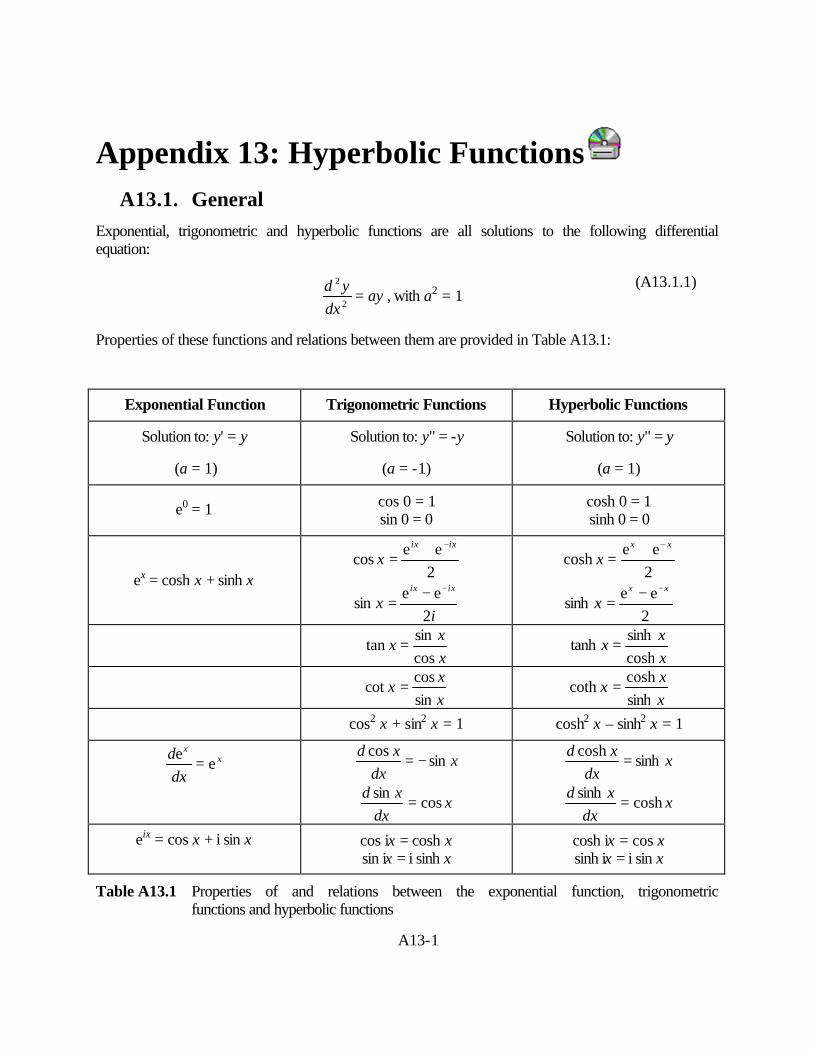
A13-1
Appendix 13: Hyperbolic Functions A13.1. General
Exponential, trigonometric and hyperbolic functions are all solutions to the following differential equation:
ay
dxyd
=2
2
, with a2 = 1 (A13.1.1)
Properties of these functions and relations between them are provided in Table A13.1:
Exponential Function Trigonometric Functions Hyperbolic Functions
Solution to: y' = y
(a = 1)
Solution to: y" = -y
(a = -1)
Solution to: y" = y
(a = 1)
e0 = 1 cos 0 = 1 sin 0 = 0
cosh 0 = 1 sinh 0 = 0
ex = cosh x + sinh x 2ee
cosixix
x−+
=
ix
ixix
2ee
sin−−
=
2ee
coshxx
x−+
=
2ee
sinhxx
x−−
=
xx
xcossin
tan = xx
xcoshsinh
tanh =
xx
xsincos
cot = xx
xsinhcosh
coth =
cos2 x + sin2 x = 1 cosh2 x – sinh2 x = 1
xx
dxd
ee
= xdx
xdsin
cos−=
xdx
xdcos
sin=
xdx
xdsinh
cosh=
xdx
xdcosh
sinh=
eix = cos x + i sin x cos ix = cosh x sin ix = i sinh x
cosh ix = cos x sinh ix = i sin x
Table A13.1 Properties of and relations between the exponential function, trigonometric functions and hyperbolic functions
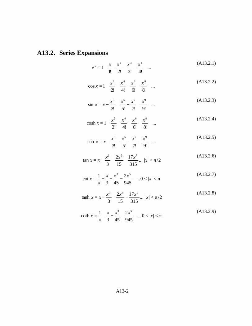
A13-2
A13.2. Series Expansions
...
!4!3!2!11
432
+++++=xxxx
e x (A13.2.1)
...
!8!6!4!21cos
8642
++−+−=xxxx
x (A13.2.2)
...
!9!7!5!3sin
9753
++−+−=xxxx
xx (A13.2.3)
...
!8!6!4!21cosh
8642
+++++=xxxx
x (A13.2.4)
...
!9!7!5!3sinh
9753
+++++=xxxx
xx (A13.2.5)
...
31517
152
3tan
753 xxxxx +++= |x| < π/2
(A13.2.6)
...
9452
4531
cot53
+−−−=xxx
xx 0 < |x| < π
(A13.2.7)
...
31517
152
3tanh
753 xxxxx −+−= |x| < π/2
(A13.2.8)
...
9452
4531
coth53
++−+=xxx
xx 0 < |x| < π
(A13.2.9)

A14-1
Appendix 14: Stirling Approximation Factorials can be approximated for large values of n using the Stirling approximation which is given by:
)
1(O
2488320571
51840139
2881
121
1]exp[2! 5532 nnnnnnnnn n +−−++−= π (A14.1)
An alternate form, which is of particular interest if the logarithm of n! must be calculated is given by:
)]
1(O
121
exp[2!2nn
nnnn n ++−= π (A14.2)
The exact and approximate values for n = 1, 2, ... 20 and the relative error as calculated using (A14.1) and (A14.2) are provided in the Table A14.1.
n n! Equation (A14.1) RelativeError
Equation (A14.2) RelativeError
1 1 1.00 5.01E-04 1.00 2.27E-03 2 2 2.00 2.10E-05 2.00 3.26E-04 3 6 6.00 3.00E-06 6.00 9.99E-05 4 24 24.00 7.33E-07 24.00 4.27E-05 5 120 120.00 2.44E-07 120.00 2.20E-05 6 720 720.00 9.89E-08 720.01 1.28E-05 7 5040 5040.00 4.60E-08 5040.04 8.05E-06 8 40320 40320.00 2.37E-08 40320.22 5.40E-06 9 362880 362880.00 1.32E-08 362881.38 3.80E-06 10 3628800 3628799.97 7.79E-09 3628810.05 2.77E-06 11 39916800 39916799.81 4.84E-09 39916883.11 2.08E-06 12 479001600 479001598.50 3.14E-09 479002368.48 1.60E-06 13 6227020800 6227020786.90 2.10E-09 6227028659.89 1.26E-06 14 87178291200 87178291073.35 1.45E-09 87178379323.32 1.01E-06 15 1307674368000 1307674366653.88 1.03E-09 1307675442913.47 8.22E-07 16 20922789888000 20922789872396.30 7.46E-10 20922804061389.80 6.77E-07 17 355687428096000 355687427900040.00 5.51E-10 355687629001078.00 5.65E-07 18 6402373705728000 6402373703076830.00 4.14E-10 6402376752492220.00 4.76E-07 19 121645100408832000 121645100370383000.00 3.16E-10 121645149634119000.00 4.05E-07 20 2432902008176640000 2432902007581510000.00 2.45E-10 2432902852332160000.00 3.47E-07
Table A14.1 Value and relative accuracy of n! as calculated using (A14.1) and (A14.2)

A14-2
It is of interest to further examine the accuracy as a function of the number of terms. Figure A14.1 presents the relative error for n ranging from 1 to 100 as calculated using the first, 2, 3, 4 and 5 terms of (A14.1) as well as equation (A14.2).
Figure A14.1 Relative accuracy of n! as a function of n. Compared are the accuracy when using 1, 2, 3, 4, or 5 terms of (A14.1) and (A14.2)
From the figure one finds that there is a significant improvement in accuracy between using only the first term versus using the first two terms of the approximation. The first term results in an accuracy better than 1%, while two or more terms provide an accuracy better than 10-6 for integers larger than 15. Surprisingly there is little improvement when adding the third term. Adding the fourth and fifth term does further improve the accuracy. For most applications one will find that two terms of (A14.1) or (A14.2) will provide sufficient accuracy.
If the natural logarithm of n! is of interest it can be obtained from (A14.2), yielding:
)
1(O
121
ln)21
(2ln!ln2nn
nnnn ++−++= π (A14.3)
1.0E-14
1.0E-12
1.0E-10
1.0E-08
1.0E-06
1.0E-04
1.0E-02
1.0E+00
0 20 40 60 80 100
Number
Rel
ativ
e er
ror
1 term
2 terms, 3 terms, (A14.2)
4 terms
5 terms
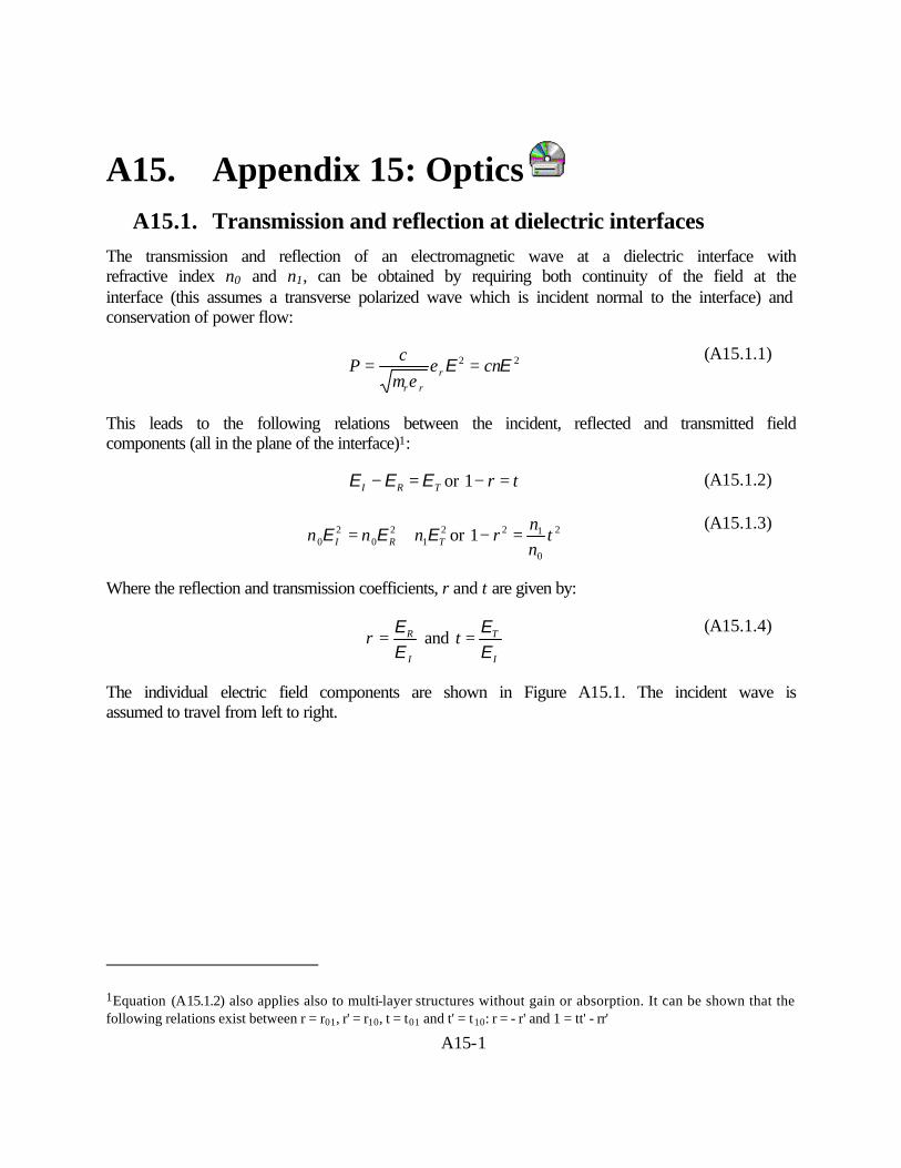
A15-1
A15. Appendix 15: Optics A15.1. Transmission and reflection at dielectric interfaces
The transmission and reflection of an electromagnetic wave at a dielectric interface with refractive index n0 and n1, can be obtained by requiring both continuity of the field at the interface (this assumes a transverse polarized wave which is incident normal to the interface) and conservation of power flow:
22 EE cnc
P rrr
== εεµ
(A15.1.1)
This leads to the following relations between the incident, reflected and transmitted field components (all in the plane of the interface)1:
TRI EEE =− or tr =−1 (A15.1.2)
21
20
20 TRI nnn EEE += or 2
0
121 tnn
r =− (A15.1.3)
Where the reflection and transmission coefficients, r and t are given by:
I
RrEE
= and I
TtEE
= (A15.1.4)
The individual electric field components are shown in Figure A15.1. The incident wave is assumed to travel from left to right.
1Equation (A15.1.2) also applies also to multi-layer structures without gain or absorption. It can be shown that the following relations exist between r = r01, r' = r10, t = t01 and t' = t10: r = - r' and 1 = tt' - rr'

A15-2
R E
E T
E I
1 n 0
x
n
Figure A15.1: Incident, reflected and transmitted wave at a dielectric interface.
These equations can be solved yielding the transmission and reflection coefficients, t01 and r01.
10
101
2nn
ntt
I
T
+===
EE
(A15.1.5)
And
10
100101 1
nnnn
trrI
R
+−
==−==EE
(A15.1.6)
where the subscripts 0 and 1 are used to indicate that the incident wave travels from the material with index n0 towards the material with index n1. The fraction of the power reflected, R, and transmitted, T, are given by:
2
10
210
20
20
)()(
nnnn
nn
PP
RI
R
I
R
+−
===EE
(A15.1.7)
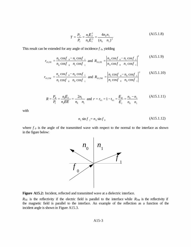
A15-3
2
10
102
0
21
)(4
nnnn
nn
PP
TI
T
I
T
+===
EE
(A15.1.8)
This result can be extended for any angle of incidence φ0, yielding
1100
1100,01 coscos
coscosφφφφ
nnnn
r TE +−
= and 2
1100
1100,01 coscos
coscosφφφφ
nnnn
R TE +−
= (A15.1.9)
1001
100,01 coscos
coscos
φφ
φφ
nn
nnr q
TM +
−= and
2
1001
1001,01 coscos
coscosφφφφ
nnnn
R TM +−
= (A15.1.10)
10
1
0
0 2nn
nnn
PP
R T
I
R
+===
EEE
and 10
100101 1
nnnn
trrI
R
+−
==−==EE
(A15.1.11)
with
0011 sinsin φφ nn = (A15.1.12)
where φ0 is the angle of the transmitted wave with respect to the normal to the interface as shown in the figure below:
n 0 n 1
φ 0
φ 1
Figure A15.2: Incident, reflected and transmitted wave at a dielectric interface.
RTE is the reflectivity if the electric field is parallel to the interface while RTM is the reflectivity if the magnetic field is parallel to the interface. An example of the reflection as a function of the incident angle is shown in Figure A15.3.

A15-4
Incident Angle [Degrees]
Ref
lect
ion
0
0.1
0.2
0.3
0.4
0.5
0.6
0.7
0.8
0.9
1
0 10 20 30 40 50 60 70 80 90
Figure A15.3 Reflectivity at an air-GaAs interface (n0 = 1, n1 = 3.5) as a function of the incident angle for both polarizations (TE and TM) of the incident wave. The reflectivity, RTM goes to zero if the incident angle equals tan-1 (n1/n0)
A15.2. Transmission and reflection of a multi-layer dielectric structure
In order to calculate the reflection and transmission of a multi-layer structure, we first define the electric field components left and right of the first interface: two field components corresponding to the forward propagating waves, E0,f and E’1,f and two field components corresponding to the backward propagating waves, E0,b and E’1,b. All field components are assumed to be parallel to the plane of the interface.
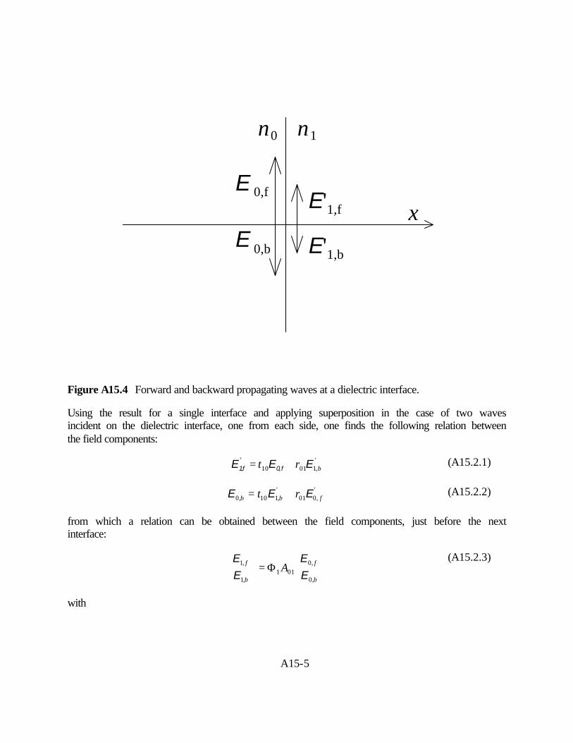
A15-5
0,b E
E' 1,f
E 0,f
E' 1,b
n 1 n 0
x
Figure A15.4 Forward and backward propagating waves at a dielectric interface.
Using the result for a single interface and applying superposition in the case of two waves incident on the dielectric interface, one from each side, one finds the following relation between the field components:
',10110 brt EEE f0,
'f1, += (A15.2.1)
',001
',110,0 fbb rt EEE += (A15.2.2)
from which a relation can be obtained between the field components, just before the next interface:
Φ=
b
f
b
f A,0
,0011
,1
,1
EE
EE
(A15.2.3)
with

A15-6
+−−+
=0101
0101
101 2
1nnnnnnnn
nA and
=Φ
− 11
11
00
1 dik
dik
ee
(A15.2.4)
The matrix Φ1 accounts for the phase shift through the layer with index n1 and thickness d1. Note that that A01A10 should equal a unity matrix so that A10
-1 = A01.
This result can easily be extended to a set of N interfaces for which
ΦΦΦΦ=
−−−−
b
fNNNNNN
bN
fN AAAA,0
,00111221,21,1
,
, ...EE
EE
(A15.2.5)
15.2.1. Example: a Distributed Bragg Reflector (DBR)
Consider a DBR structure consisting of N periods of two quarter-wavelength layers with alternating index n1 and n2, between layers with index n0 and n3. The relation between the field components just after the last interface and those just before the first interface is given by:
ΦΦ=
b
fN
b
f AAAAA,0
,0011122211223 ][
EE
EE
(A15.2.6)
The subscripts refer to the index of refraction left and right of the interface. The matrix A12 was added to cancel the last matrix A21 of the Nth product. The Nth power of the matrices characterizing one period of the DBR is given by:
+−
−+−
=ΦΦ−−
−−
NNNN
NNNNN
N
nn
nn
nn
nn
nn
nn
nn
nn
AA)()()()(
)()()()(
2)1(
][
2
1
2
1
2
1
2
1
2
1
2
1
2
1
2
1
112221
(A15.2.7)
assuming Φ1 and Φ2 to equal
− i
i0
0, as is the case for quarter-wavelength layers, yielding:
+−
−+−
=
−−
−−
b
f
NNNN
NNNNN
b
f
nn
nn
nn
nn
nn
nn
nn
nn
nn
nn
nn
nn
,0
,0
2
1
2
1
0
3
2
1
2
1
0
3
2
1
2
1
0
3
2
1
2
1
0
3
)()()()(
)()()()(
2)1(
EE
EE
(A15.2.8)
The total reflectivity of the structure can be obtained by requiring Eb to be zero so that

A15-7
2
2
2
1
0
3
2
2
1
0
3
2
2
)(1
)(1
+
−===
N
N
I
R
nn
nn
nn
nn
PP
R0f
0b
E
E
(A15.2.9)
15.2.2. Spreadsheet solution to an arbitrary layer structure
The matrix for an arbitrary layer with index n1 and thickness d1 following a layer with index n0 can be written as a function of the real and imaginary components of the fields:
Re(E1f) = cosφ1 (a11Re(E0f) + a12Re(E0b))
-sinφ1 (a11Im(E0f) + a12Im(E0b))
Im(E1f) = sinφ1 (a11Re(E0f) + a12Re(E 0b))
+ cosφ1 (a11Im(E0f) + a12Im(E0b))
Re(E1b) = cosφ1 (a12Re(E0f) + a11Re(E0b))
+ sinφ1 (a12Im(E0f) + a11Im(E0b))
Im(E1b) = - sinφ1 (a12Re(E0f) + a11Re(E0b))
+ cosφ1 (a12Im(E0f) + a11Im(E0b))
with φ1 = k1d1 and a11= 1
01
2nnn +
a12 = 1
01
2nnn −
(A15.2.10)
This set of equations can also be interpreted as a recursion relation between the fields at the end of the current layer and the fields at the end of the previous layer. The field within a given layer is obtained by dividing this layer into different section with the same index of refraction and a combined thickness, which equals the layer thickness. Implementation into a spreadsheet provides the actual fields throughout the structure. An example is shown in Figure A15.5:

A15-8
Distance [micron]In
dex,
Rea
l par
t, Im
agin
ary
part
and
ampl
itude
of t
he F
ield
-6
-4
-2
0
2
4
6
0 0.5 1 1.5 2
Figure A15.5 Refractive index as well as real part, imaginary part and amplitude of the total field due to the forward and backward propagating waves. The incident wave is a forward propagating wave with unity amplitude and zero phase at x = 0
15.2.3. Reflection and transmission through multiple layers
The calculation of the reflection and transmission through multiple layers can in general be obtained by using equation (A15.2.5), assuming that no incident wave is present after the Nth interface or ENb = 0, as was used to calculate the reflection of a distributed Bragg reflector in section A15.2.1 For the general case this requires inverting the matrix linking the incident fields E0f and E0b to the fields on the other side of the structure, ENf and ENb. This procedure can be avoided by using the time reversal principle, which applies in the absence of magnetic fields, so that setting the incident fields equal to:
10 =fE and 00 =bE (A15.2.11)
one finds the reflection, R, and transmission, T, through the structure from:
2
2
Nf
NbRE
E= and
20
1
Nf
N
nn
TE
= (A15.2.12)

A15-9
These expressions can even be applied to the case where some or even all the layers are absorbing or have gain, by using the complex conjugate of the refractive indices: As the waves travel through the structure in the reverse direction, one finds that absorbing regions provide gain while regions with gain become absorbing. Inverting the sign of the imaginary part of the refractive index for each region therefore provides the correct absorption/gain when reversing time. An example for the case of a thin silver layer is shown in Figure A15.6.
Wavelength [nm]
Ref
lect
ion,
Tra
nsm
issi
on a
ndA
bsor
ptio
n [%
]
0
10
20
30
40
50
60
70
80
90
100
500 700 900 1100 1300 1500
R
A
T
Figure A15.6 Reflection, R, transmission, T, and absorption, A, versus wavelength of a 10 nm silver layer in air. The refractive index of the silver was assumed to be n = 0.102 + i 6.22.
A15.3. Fabry-Perot cavity Consider a structure consisting of two reflecting interfaces with reflection coefficients r01 and r12, transmission coefficients t01 and t12. The two reflecting surfaces are separated by a medium with thickness d, refractive index n and absorption coefficient α. The reflection and transmission amplitudes are given by2:
δ
δ
i
i
I
R
errerr
AA
−
−
++
=1201
1201
1 ,
δ
δ
i
i
I
T
errett
AA
−
−
+=
1201
2/1201
1
(A15.3.1)
2See Yariv, "Optical Electronics", Fourth edition, Holt Reinhart and Winston, Inc, 1991, p 112-115.

A15-10
For a symmetric structure with r01 = - r12 and t01 = t12 one obtains the following reflection, transmission and absorption intensities.
Reflection =
22
2
*
*
cos21)cos21(
ARRAAAR
AAAA
II
II
RR
I
R
+−+−
==δ
δ
(A15.3.2)
Transmission =
22
2
*
*
cos21)1(
ARRARA
AAAA
II
II
TT
I
T
+−−
==δ
(A15.3.3)
Absorption =
22
22
cos21))1()1(cos2(
ARRARARRA
+−−−+−
δδ
(A15.3.4)
with
0
0
coscos4
φα
λφπ
δd
ind
−= , 0cos/e φαdA −= (A15.3.5)
These equations enable to calculate reflection, transmission and absorption as a function of
cavity length or as a function of photon energy, Eph [eV] = λq
hc. Examples are shown in the
following figures:

A15-11
Cavity Length [micron]
Ref
lect
ion,
Tra
nsm
issi
on a
ndA
bsor
ptio
n
0
0.1
0.2
0.3
0.4
0.5
0.6
0.7
0.8
0.9
1
0 0.1 0.2 0.3 0.4
T
R
A
Figure A15.7 Reflection, Transmission and Absorption versus cavity length of a GaAs Fabry-Perot cavity at 830 nm under normal incidence.
Photon Energy [eV]
Ref
lect
ion
and
Tra
nsm
issi
on
0
0.1
0.2
0.3
0.4
0.5
0.6
0.7
0.8
0.9
1
1.4 1.402 1.404 1.406 1.408 1.41

A15-12
Figure A15.8 Reflection and transmission versus photon energy of a 100 µm GaAs Fabry-Perot cavity under transparency conditions (i.e. α = 0)
A15.4. Ellipsometer Equations An ellipsometer enables to measure the refractive index and the thickness of semi-transparent thin films. The instrument relies on the fact that reflection at a dielectric interface depends on the polarization of the light. It consists of a laser whose state of polarization can be modified with a polarizer. The beam is reflected off the layer of interest and then analyzed with a polarizer. The operator changes the angle of the polarizer and analyzer until a minimal signal is detected. The angles are then related to the reflections for both polarizations in the following way:
∆Ψ= i
TE
TM
rr
etan (A15.4.1)
The angles Ψ and ∆ are related to the measured angles, P1, A1, P2 and A2 in the following way:
2121 22
25
22
3PPPP −−=−=−=∆ π
ππ
(A15.4.2)
221
21
ππ
+−=−==Ψ
AAAA
(A15.4.3)
The minimal signal is obtained when both polarization incident on the analyzer are in phase. This can be obtained for two different positions of the polarizer, hence the two values P1 and P2. In principle one could measure either one. In practice both values are measured to eliminate any possible misalignment of the instrument thereby yielding a more accurate result.
A theoretical analysis of the Ψ−∆ curves is obtained by combining the expressions for the reflectivities at both dielectric interfaces (A15.1.9) and (A15.1.10) with the expression for the asymmetric Fabry-Perot cavity (A15.3.1). An example of such curves as obtained for silicon dioxide layers (n1 = 1.455) on silicon (n2 = 3.875 – i 0.018) using a helium-neon laser (λ = 0.6328 µm) is in Figure A15.9.

A15-13
Psi
Del
ta
60
120
180
240
300
0 10 20 30 40 50 60 70 80 90
Figure A15.9 Ψ-∆ curves for silicon dioxide on silicon. Thickness increases counter clock wise from 0 (square marker on the left) in steps of 10 nm (black diamonds) and in steps of 100 nm (squares). Incident angle of the laser beam is 70 degrees.
Since the silicon dioxide was assumed to be transparent one finds the values for both Ψ and ∆ to
be identical for layers which differ in thickness by 11 cos2 φ
λn
= 0.284 µm. The corresponding
curves for the measured values P1, A1, P2 and A2 are also shown in Figure A15.10:

A15-14
A1, A2
P1,
P2
-20
0
20
40
60
80
100
120
140
160
180
200
0 20 40 60 80 100 120 140 160 180
Figure A15.10A1-P1 and A2-P2 curves for silicon dioxide on silicon. Thickness increases counter clock wise from 0 (at the square marker on the left) for A1 versus P1 and counter clock wise from 0 (square marker on the right) for A2 versus P2, both in steps of 10 nm (black diamonds) and in steps of 100nm (squares). Incident angle of the laser beam is 70 degrees from the normal to the surface.

A15-15
A15.5. Interference colors of thin transparent films Transparent thin films often have strikingly bright colors, which vary rapidly with thickness. These colors are caused by interference of the light reflected at the front and back interface of the film and vary depending on the refractive index of the film as well as that of the substrate. The analysis is simply based on the general expressions for the Fabry-Perot cavity (A15.3.1), which can be further manipulated to yield the total reflectivity as a function of the wavelength.
2
122
011201
2121201
201
*
*
cos21cos2
)(rrrrrrrr
AAAA
nRII
RR
++++
==δ
δλ
(A15.5.1)
With
λφπ
δ 11 cos4 dn=
(A15.5.2)
The reflection can then be calculated as a function of the wavelength corresponding to the primary colors red, green and blue. A useful way to eliminate one of the primary colors in the determination of the observed color is by determining the intensity of white light as an equal amount of red, green and blue light. The actual colors observed for each thickness depend on the relative intensities of the remaining primary colors. An example is shown in the figure below for silicon dioxide on a silicon substrate.
Figure A15.11 Relative intensities of the colors reflected off a silicon dioxide layer on a silicon substrate.
Table A15.1 lists the color as a function of the thickness for some different materials.
Film thickness [nm]
Ref
lect
ivit
y [%
]
0
5
10
15
20
25
30
35
0 100 200 300 400 500 600 700 800 900 1000
1 / 1.5 / 3.875

A15-16
air/ water/ air
n0 / n1 / n2
1 / 1.33 / 1
air / water / glass
n0 / n1 / n2
1 / 1.33 / 1.5
< 10 nm black < 10 nm White
100nm white 100 nm Black
150 nm brownish-yellow 150 nm Blue
200 nm violet 210 nm White
250 nm blue 230 nm Yellow
300 nm light green 270 nm Red
330 nm orange 360 nm Blue
400 nm pink 400 nm Green
450 nm light blue 450 nm Yellow
500 nm dark green 500 nm Red
600 nm red 530 nm Pink
650 nm turquoise 610 nm Green
Table A15.1: Expected color versus thickness for thin layers of water in air or on a glass surface

A16-1
A16. Appendix 16: Equation Sheet
Chapter 1: Review of Modern Physics
1.2. Quantum mechanics
ph
=λ λ
ωνhc
hE ph === h
)()()()(
2 2
22
xExxVdx
xdm
Ψ=Ψ+Ψ
−h
... 2, 1, with , )2
(2
2*
2
== nLn
mh
Ex
n ... 2, 1, with , 8 222
0
40 =−= n
nh
qmEn
ε
1.3. Electromagnetic theory
ερ )()( x
dxxd
=E
)()(
xdx
xd E−=φ
ερφ )()(
2
2 x
dx
xd−=

A16-2
Chapter 2: Semiconductor Fundamentals
2.3. Energy bands
βα
+−=
TT
ETE gg
2)0()(
2.4. Density of states
ccc EEEEmhdE
dN
LEg ≥−== for ,
281)(
2/3*33
π
cc EEEg <= for ,0)(
2.5. Carrier distribution functions
kTEEE
Ff
/)()(
e1
1−+
=
kTEEEdonor
Fddf
/)(21
)(e1
1−+
=
kTEEEacceptor
Faaf
/)()(
e41
1−+
=
1e
1/)(
)(−
=− kTEE
EBEF
f kTEE
EMBF
f/)(
)(e
1−
=
2.6. Carrier densities
∫=∞
cco
EdEEfEgn )()(
∫ −=∞−
vE
vo dEEfEgp )](1)[(
cFcFo EEEEm
n ≥−
= for ,)(
232 2/3
2/3
2
*
2 hπand T = 0 K

A16-3
kTEE
co
cF
eNn−
= with 2/32
*]
2[2
h
kTmN e
cπ
= kTEE
vo
Fv
eNp−
= with 2/32
*]
2[2
h
kTmN h
vπ
=
kTEvci
geNNn2/−
= 2ioo npn =⋅
)ln(43
2)ln(
21
2 *
*
e
hvc
c
vvci m
mkT
EENN
kTEE
E ++
=++
=
kTEEio iFenn /)( −= kTEE
io Fienp /)( −=
i
oiF n
nkTEE ln+=
i
oiF n
pkTEE ln−=
eV 6.132
0
*
r
conddc
m
mEE
ε=−
22)2
(2 i
adado n
NNNNn +
−+
−=
−+−+
22)2
(2 i
dadao n
NNNNp +
−+
−=
+−+−
)exp(kT
EFnnnn in
io−
=+= δ )exp(kT
FEnppp pi
io
−=+= δ
2.7. Carrier Transport
mqv τ
µ =∆=
||
||
Err
α
µµµµ
minmaxmin
)(1rN
N+
−+=
Err
nnqJ µ= E)( pnhe pnqvpqvnqJ µµ +=+=
)( pn pnqJ
µµσ +==∆
E )(
11pnq pn µµσ
ρ+
==

A16-4
satv
vE
EEµ
µ
+=
1)(
dxdn
DqJ nn = dxdp
DqJ pp −=
tnnn Vq
kTD µµ == tppp V
qkT
D µµ ==
dxdn
DqnqJ nnn += Eµ dxdp
DqpqJ ppp −= Eµ
)( pntotal JJAI +=
2.8. Carrier recombination and generation
n
ppnnn
nnGRU
τ0−
=−= p
nnppp
ppGRU
τ0−
=−=
)( 2ibb nnpbU −=− σtht
tii
iSHR vN
kTEE
nnp
npnU
)cosh(2
2
−++
−=
)()( 22ipinAuger nnppnnpnU −Γ+−Γ=
AE
xPGG
ph
optlightnlightp
)(,, α==
)()(
xPdx
xPdopt
opt α−=
2.9. Continuity equation
),(),(),(),( 1 txRtxG
xtxJ
ttxn
nnn
q−+
∂∂
=∂
∂ ),(),(
),(),( 1 txRtxGx
txJ
ttxp
ppp
q−+
∂
∂−=
∂∂
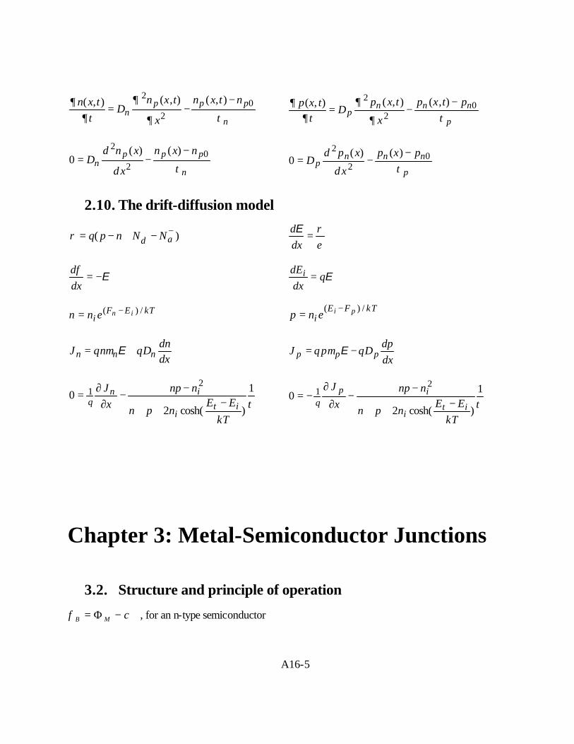
A16-5
n
pppn
ntxn
x
txnD
ttxn
τ∂
∂
∂∂ 0
2
2 ),(),(),( −−=
p
nnnp
ptxp
x
txpD
ttxp
τ∂
∂∂
∂ 02
2 ),(),(),( −−=
n
pppn
nxn
xd
xndD
τ0
2
2 )()(0
−−=
p
nnnp
pxp
xd
xpdD
τ0
2
2 )()(0
−−=
2.10. The drift-diffusion model
)( −+ −+−= ad NNnpqρ ερ
=dxdE
E−=dxdφ
Eqdx
dEi =
kTEFi inenn /)( −=
kTFEi
pienp/)( −
=
dxdn
DqnqJ nnn += Eµ dxdp
DqpqJ ppp −= Eµ
τ1
)cosh(20
21
kTEE
npn
nnpxJ
iti
inq −
++
−−
∂∂
= τ1
)cosh(20
21
kTEE
npn
nnpx
J
iti
ipq −
++
−−
∂
∂−=
Chapter 3: Metal-Semiconductor Junctions
3.2. Structure and principle of operation
χφ −Φ= MB , for an n-type semiconductor

A16-6
Mg
B q
EΦ−+= χφ , for a p-type semiconductor
type-n , ,
q
EE nFcMi
−−−Φ= χφ type-p , -,
MpFc
i q
EEΦ
−+= χφ
3.3. Electrostatic analysis
)(2
2−+ −+−−=−= ad
ssNNnp
q
dx
dεε
ρφ
)sinh(sinh2
2
2
t
F
t
F
s
iVV
nq
dx
d φφφε
φ+
−=
i
da
t
Fn
NN
V 2sinh
+− −=
φ
xxx
xxqNx
d
dd
<=
<<=
0)(
0 )(
ρ
ρ
xxx
xx(xqN
x
d
dds
d
≤=
<<−=
0)(
0 x)-)(
E
Eε
xxxqN
x
xx-x)(xxqN
x
xx
ds
dd
ddds
d
≤=
<<−=
≤=
2
)(
0 ][2
)(
0 0)(
2
22
εφ
εφ
φ
s
d
s
dd QxqNx
εε−=−== )0(E
s
ddai
xqNxV
εφφ
2)0(
2
==−=−
d
aisd qN
Vx
)(2 −=
φε
d
s
ai
ds
a
dj xV
NqdVdQ
Cε
φε
=−
==)(2
3.4. Schottky diode current
]1))[exp(exp(max −−=t
a
t
Bcnn V
VV
NqJφ
µ E s
dai NVqε
φ )(2max
−=E

A16-7
]1))[exp(exp( −−=t
a
t
BcRn V
VV
NqvJφ
m
kTvR π2
=
Θ= nvqJ Rn
−=Θ
E
2/3*234
exp Bqm φh
Chapter 4: p-n Junctions
4.2. Structure and principle of operation
2ln
i
adti
n
NNV=φ ai V−= φφ
4.3. Electrostatic analysis of a p-n diode
pnd xxx +=
npadad xxxNNqNNnpq ≤≤−−≅−+−= −+−+ for ,)()(ρ
0)(
)(
)(
0)(
=
=
−=
=
x
qNx
qNx
x
d
a
ρ
ρ
ρ
ρ
xx
xx
xx
xx
n
n
p
p
≤
≤≤
≤≤−
−≤
for ,
0for ,
0for ,
for ,
ndn xqNQ = pap xqNQ −=
npadss
xxxxNxNqx
dx(x)d
≤≤−−≅= −+ for ,))()(()(
εερE

A16-8
0)(
)()(
)()(
0)(
=
−=
+−=
=
x
xxqNx
xxqNx
x
s
nd
s
pa
E
E
E
E
ε
ε
xx
xx
xx
xx
n
n
p
p
≤
≤≤
≤≤−
−≤
for ,
0for ,
0for ,
for ,
s
nd
s
pa xNqxNqx
εε−=−== )0(E
d
ai
xV
x)(2
)0(−
−==φ
E
pand xNxN =
da
adn NN
Nxx
+=
da
ddp NN
Nxx
+=
s
pa
s
ndai
xNqxNqV
εεφ
22
22
+=− ))(11
(2
aida
sd V
NNqx −+= φ
ε
)(12
aidad
asn V
NNNN
qx −
+= φ
ε )(
12ai
daa
dsp V
NNNN
qx −
+= φ
ε
da
da
ai
sj NN
NNV
qC
+−=
)(2 φε
d
sj x
Cε
=
4.4. The p-n diode current
ta VVnnn epxxp /
0)( == ta VVppp enxxn /
0)( =−=
pnpn LxxLxxnnn eBeApxxp
/)(/)(0)(
−−−++=≥
pppp LxxLxxppp eDeCnxxn /)(/)(
0)( ++− ++=−≤

A16-9
]sinhcothcosh)[1()('
/00
p
n
p
n
p
nVVnnnn L
xxLw
Lxx
eppxxp ta−
−−
−+=≥
]sinhcothcosh)[1()('
/00
n
p
n
p
n
pVVpppp L
xx
L
w
L
xxennxxn ta
++
+−+=−≤
nnn xww −=' ppp xww −='
)1(])()([ / −≅+=+−== ta VVsrnppn eIJxxJxxJAI
)]coth()coth(['0
'0
p
n
p
np
n
p
n
pns L
wL
pD
L
w
L
nDAqI += (general case)
][ 00
p
np
n
pns L
pD
L
nDAqI += (“long” diode) ][ '
0'
0
n
np
p
pns
w
pD
w
nDAqI += (“short” diode)
)1( /2 −=−ta VV
ibb ewbnqJ )1(2
2/'
−= ta VViSHR e
xqnJ
τ
saa IRVV +=*
ta VVs eJJ η/=
mV/decade 59.6slope
1
slope )elog(
==tV
η
pVV
psptaIQ τ)1e( /
, −=∆ p
pnps L
DpAqI 0
, =
t
pVV
pspd V
IC
ta τ/,
,
e= (“long” diode)
t
prVV
pspd V
tIC
ta,
/,
,
e= (“short” diode) with
p
ppr D
wt
2
2'
, =
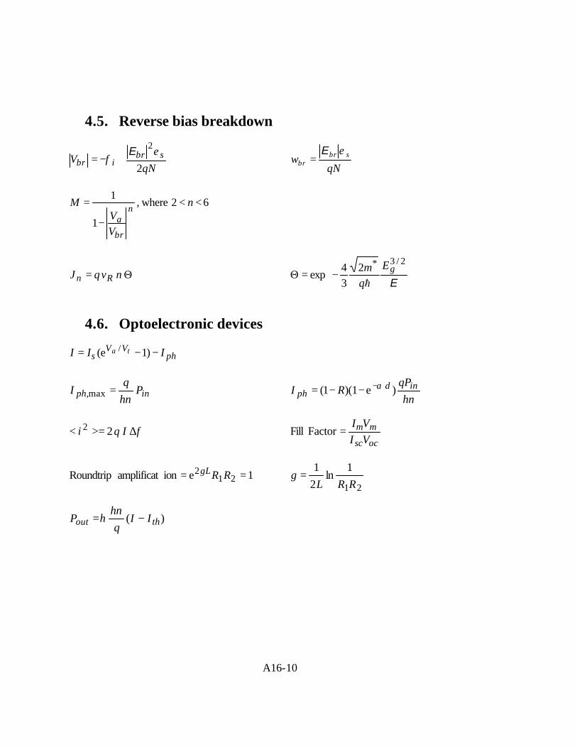
A16-10
4.5. Reverse bias breakdown
qNV sbr
ibr 2
2εφ
E+−=
qNw sbr
brεE
=
6 2 where,
1
1<<
−
= n
VV
Mn
br
a
Θ= nvqJ Rn
−=Θ
E
2/3*234
exp gE
qmh
4.6. Optoelectronic devices
phVV
s III ta −−= )1e( /
inph Phq
Iν
=max, ν
αh
qPRI ind
ph )e1)(1( −−−=
fIqi ∆>=< 22 ocsc
mmVIVI
=Factor Fill
1e ion amplificat Roundtrip 212 == RRgL
21
1ln
21
RRLg =
)( thout IIq
hP −=
νη

A16-11
Chapter 5: Bipolar Junction Transistors
5.2. Structure and principle of operation
BEnEE xww ,' −= BCpBEpBB xxww ,,
' −−=
BCnCC xww ,' −=
+
−=
EBE
BBEBEisBEn NNN
Nq
Vx
1)(2 ,,
φε
+
−=
EBB
EBEBEisBEp NNN
Nq
Vx
1)(2 ,,
φε
+
−=
CBB
CBCBCisBCp NNN
Nq
Vx
1)(2 ,,
φε
+
−=
CBC
BBCBCisBCn NNN
Nq
Vx
1)(2 ,,
φε
2, lni
EBtBEi n
NNV=φ 2, ln
i
CBtBCi n
NNV=φ
BCE III += drpEnEE IIII ,,, ++=
BrnEC III ,, −= drBrpEB IIII ,,, ++=
E
CII
=α α
αβ
−==
1B
CII
rET δγαα = pEnE
nEE II
I
,,
.+
=γ
nI
II
E
BrnET ,
,, −=α
E
drEr I
II ,−=δ

A16-12
5.3. Ideal transistor model
−
= 1)exp(
',2
,t
BE
BB
BnEinE V
V
wN
DAqnI
−
= 1)exp(
',2
,t
BE
EE
EpEipE V
V
wN
DAqnI
21)exp(
'2
,B
t
BE
B
iEBn
wV
VNn
AqQ
−=∆
n
BnBr
QI
τ,
,∆
=
r
BnnE t
QI ,
,∆
= Bn
Br D
wt
,
2'
2=
',
',
1
1
EEBn
BBEpE
wND
wND+
=γ nBn
B
n
rT D
wtττ
α,
2'
211 −=−=
EBBEp
EEBn
wND
wNDγαβ ≅≅ if ,
',
',
BCnBCp
s
BB
BCj
BA
xx
wqNCQ
V
,,
'
,
+
==ε
BEjB
t
BE
Ct
CQV
dVId
Vn ,1
ln1
+≅=
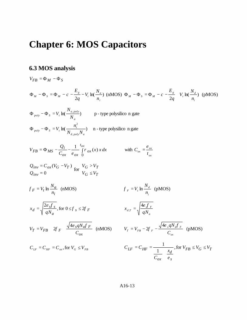
A16-13
Chapter 6: MOS Capacitors
6.3 MOS analysis
SMFBV Φ−Φ=
)ln(2 i
at
gMSM n
NV
q
E−−−Φ=Φ−Φ χ (nMOS) )ln(
2 i
dt
gMSM n
NV
q
E+−−Φ=Φ−Φ χ (pMOS)
gaten polysilico type-n )ln(
gaten polysilico type-p )ln(
,
2
,
apolyd
itSpoly
a
polyatSpoly
NNn
V
N
NV
=Φ−Φ
=Φ−Φ
∫−−Φ=oxt
oxoxox
iMSFB dxxx
CQ
V0
)(1
ρε
with ox
oxox t
Cε
=
0)(
=−=
inv
TGoxinvQ
VVCQ for
TG
TGVVVV
≤>
i
atF n
NV ln=φ (nMOS)
i
dtF n
NV ln=φ (pMOS)
Fsa
ssd Nq
x φφφε
20for ,2
≤≤= a
FsTd Nq
xφε4
, =
ox
FasFFBT C
qNVV
φεφ
42 ++= (nMOS)
ox
FdsFFBT C
qNVV
φεφ
42 −−= (pMOS)
FBGoxHFLF VVCCC ≤== for , TGFB
s
d
ox
HFLF VVVx
C
CC ≤≤+
== for ,1
1
ε

A16-14
TG
s
Td
ox
HFoxLF VVx
C
CCC ≥+
== for ,1
1 and
,
ε
s
D
ox
FB LC
C
ε+
=1
1 with
a
tsD qN
VL
ε=
Chapter 7: MOS Field Effect Transistors
7.3. MOSFET analysis Linear model
)(||for ,)( TGSDSDSTGSoxD VVVVVVL
WCI −<<−= µ
Quadratic model
TGSDSDSTGSoxD VVVV
VVVLW
CI DS −<−−= for , ]2
)[(2
µ
TGSDSTGS
oxsatD VVVVV
LW
CI −>−
= for , 2
)( 2
, µ
DSoxquadm VL
WCg µ=, )(, TGSoxsatm VV
LW
Cg −= µ
)(, DSTGSoxquadd VVVL
WCg −−= µ 0, =satdg

A16-15
Channel length modulation
TGSDSDSTGS
oxsatD VVV)V(VV
LW
CI −>+−
= for , 12
)( 2
, λµ
Variable depletion layer model
))2()2((232
)2
2(
2323SBFDBFasn
DSDS
FFBGSoxn
D
VVqNLW
VV
VVL
WCI
+−+−
−−−=
φφεµ
φµ
1)(2122
2, −−+−−−= FBGBsa
ox
ox
saFFBGSsatDS VV
qNC
C
qNVVV
εε
φ
)(*, TGSoxnsatm VV
LW
Cg −= µ
++
−=
sa
oxSBF
nn
qNCV
εφ
µµ2
*
)2(21
11
7.4. Threshold voltage
)2)2(( FSBFT VV φφγ −+=∆ ox
as
C
qNεγ
2=
7.7. Advanced MOSFET issues
)exp(t
TGD V
VVI
−∝
3/1−∝ Esurfaceµ

Appendix 5
Title Page Table of Contents Help Copyright B. Van Zeghbroeck, 2004
Appendix:
Comprehensive Glossary
Name
- A - A B C D E F G H I J K L M N O P Q R S T U V W X Y Z
Abrupt p-n junction p-n junction with a step function doping profile
Acceptor An atom which is likely to take on one or more electrons when placed in a crystal
Accumulation Accumulation of free carriers in a semiconductorApplied bias Voltage applied to the structure
Avalanche breakdown Breakdown mechanism caused by impact ionization leading to avalanching due to carrier multiplication
- B - A B C D E F G H I J K L M N O P Q R S T U V W X Y Z
Bandgap The range of energies between existing energy bands where no energy levels exist
Blackbody radiation Radiation from an object due to thermal energy
Body EffectThe variation of the threshold voltage of an FET due to a variation of the substrate or bulk voltage. See also Body Effect
Bohr model Model for the hydrogen atom as proposed by Niels Bohr
Bohr radiusRadius of the electron orbit in a hydrogen atom corresponding to the lowest energy energy solution of the Bohr model
Breakdown field Electric field at breakdown
Built-in potentialPotential across a structure in thermal equilibrium. The built-in potential equals the difference in work function of the two outer regions.
Built-in potential Potential across a p-n diode in thermal equilibrium.
Bulk Back contact of a MOSFET also referred to as the substrate contact.
- C - A B C D E F G H I J K L M N O P Q R S T U V W X Y Z
Capacitance Charge per unit voltage
Channel implant Ion implantation in the channel region used to adjust the threshold voltage of a MOSFET.
http://ece-www.colorado.edu/~bart/book/book/append/glossary.htm (1 of 8)11/10/2004 17:24:41
Appendix 5
Channel length modulationVariation of the channel due to an increase of the depletion region when increasing the drain voltage. A reduction of the channel yields a higher current.
CMOS Complementary metal oxide silicon (transistor)Compensation The process of adding donors and acceptor to a crystal Conduction band Lowest empty or partially filled band in a semiconductor Conductivity The ratio of the current density to the applied electric field
Continuity equation Equation which states that the rate of change of a density of particles equals the net flux of particles coming in
Crystal A solid which consists of atoms placed in a periodic arrangment
Crystalline Made of one or multiple crystalsC-V measurement Capacitance versus voltage measurement
- D - A B C D E F G H I J K L M N O P Q R S T U V W X Y Z
de Broglie wavelength Wavelength of a particle λ = h/p
Debye length Characteristic length over which the carrier density in a semiconductor changes by a factor e
Density of states The density of electronic states per unit energy and per unit volume
Depletion Removal of free carriers in a semiconductor
Depletion layer width Width of the region close to the p-n junction without free carriers
Depletion mode FET Transistor, which is normally on if the gate is connected to the source
Depletion region of a p-n diode Region close to the p-n junction without free carriersDIBL Drain induced barrier loweringDiffusion Motion of particles caused by thermal energy
Diffusion length Average distance minority carriers travel in a quasi-neutral region before they recombine
Donor An atom which is likely to give off one or more electrons when placed in a crystal
Drain Contact region of a MOSFET to which the electrons in the channel flow
DRAM Dynamic random access memoryDrift Motion of carriers caused by an electric field
- E - A B C D E F G H I J K L M N O P Q R S T U V W X Y Z
EAPROM Electrically alterable programmable read only memoryEdge effectsEEPROM Erasable electrically programmable read only memory
http://ece-www.colorado.edu/~bart/book/book/append/glossary.htm (2 of 8)11/10/2004 17:24:41

Appendix 5
Electron Particle with spin 1/2 and carrying a single negative charge (1.6 x 10⁻¹⁹ Coulomb)
Energy band A collection of closely spaced energy levels Energy level The energy which an electron can have
Enhancement FET Transistor, which is normally off if the gate is connected to the source.
Entropy Heat divided by absolute temperature
Epitaxial layer Thin layer of a single crystalline semiconductor grown on a substrate
EPROM Electrically programmable read only memory
- F - A B C D E F G H I J K L M N O P Q R S T U V W X Y Z
FAMOS Floating gate Avalanche injection Metal Oxide Silicon (transistor)
Fermi energy
The average energy per particle when adding particles to a distribution but without changing the entropy or the volume. Chemists refer to this quantity as being the electro-chemical potential
Fermions Particles with half-integer spin FET Field Effect Transistor
Field implantDoped region under the thick field oxide, which is obtained by ion implantation with the intend to eliminate the effect of the parasitic field oxide transistor.
Flash memory
Flat bandBias conditions of an MOS capacitor for which the energy band diagram of the silicon is flat. The corresponding voltage is called the Flat band voltage
Flatband diagram Energy band diagram of a M-S junction containing no net charge
Flatband diagram Energy band diagram of a p-n diode containing no net charge
Flatband diagram Energy band diagram of a MOS capacitor containing no net charge in the semiconductor
Forward bias High current bias mode of a rectifying contact
Full-depletion approximation
A common approximation which simplifies the electrostatic analysis of semiconductor devices. Assumed is that the depletion region(s) is(are) fully depleted, with abrupt transitions to the adjacent quasi-neutral regions
- G - A B C D E F G H I J K L M N O P Q R S T U V W X Y Z
Gate Electrode of an FET, which controls the charge in the channel
http://ece-www.colorado.edu/~bart/book/book/append/glossary.htm (3 of 8)11/10/2004 17:24:41
Appendix 5
Gauss' lawOne of Maxwell's equations, stating that the gradient of the electric field equals the charge density, divided by the dielectric constant.
Generation Process by which electron-hole pairs are generated
- H - A B C D E F G H I J K L M N O P Q R S T U V W X Y Z
Heat Thermal energy
High Injection
High injection occurs by definition when, while forward biasing a p-n diode, the minority carrier density equals or exceeds the doping concentration in the semiconductor. See also High-Current Analysis.
Hole Particle associated with an empty electron level in an almost filled band
Hydrogen atom An atom consisting of a proton and an electron
- I - A B C D E F G H I J K L M N O P Q R S T U V W X Y Z
Ideal diode analysis p-n diode analysis based on recombination currents in the quasi-neutral regions
Ideal ohmic contact Metal-semiconductor contact with zero resistance
Ideality factor
A number which characterizes the slope of a current-voltage plot as measured on a semi-logarithmic scale. A slope of a factor e per thermal voltage (or 1 decade/59 mV at room temperature) is considered ideal and is assigned an ideality factor of 1. A lower slope corresponds to a higher ideality factor.
Ideality factorImpurity A foreign atom in a crystal Interface Boundary between two materials
Intrinsic carrier density The density of electrons and holes in an intrinsic semiconductor
Intrinsic semiconductor A semiconductors free of defects or impurities
InversionChange of carrier type in a semiconductor obtained by applying an external voltage. In a MOSFET, inversion creates the free carriers, which cause the drain current.
Inversion layer The layer of free carriers of opposite type at the semiconductor-oxide interface of a MOSFET
Ionization The process of adding or removing an electron to/from an atom thereby creating a charged atom (i.e. ion)
I-V characteristics Current-Voltage characteristicsI-V characteristicsI-V measurement Current versus voltage measurement
- J - A B C D E F G H I J K L M N O P Q R S T U V W X Y Z
http://ece-www.colorado.edu/~bart/book/book/append/glossary.htm (4 of 8)11/10/2004 17:24:41

Appendix 5
- K - A B C D E F G H I J K L M N O P Q R S T U V W X Y Z
- L - A B C D E F G H I J K L M N O P Q R S T U V W X Y Z
Laser diode p-n diode with an optical cavity, which emits coherent light when forward biased
Latchup High current state of a CMOS circuit caused by the parasitic bipolar transistors
LDD structure Low doped drain transistor structureLight emitting diode (LED) p-n diode which emits light when forward biasedLOCOS Local oxidation used to isolate two adjacent devices.
Long diode p-n diode with a long quasi-neutral region as compared to the minority carrier diffusion length in that region
- M - A B C D E F G H I J K L M N O P Q R S T U V W X Y Z
Majority Carrier DensityThe larger density of the two carrier types (electrons and holes). The majority carrier density is frequently - but not always - equal to the doping density.
Mass action law The law which describes the relation between the densities of species involved in a chemical reaction
Minority Carrier Density
The lower density of the two carrier types (electrons and holes). The minority carrier density is typically orders of magnitude lower than the majority carrier density, yet plays an important role in p-n diodes and bipolar transistors.
Mobility The ratio of the carrier velocity to the applied electric field momentum Mass times velocity
MOSFET Metal-Oxide-Semiconductor Field Effect Transistor. See also MOSFET
- N - A B C D E F G H I J K L M N O P Q R S T U V W X Y Z
n+ semiconductor n-type semiconductor with high donor density (< 1018 cm-3)
n- semiconductor n-type semiconductor with low donor density (< 1016 cm-3)
- O - A B C D E F G H I J K L M N O P Q R S T U V W X Y Z
Ohmic contact Metal-semiconductor contact with a linear current-voltage characteristic and low resistance
One-sided p-n junction Junction with a very large doping density on one side and a very low density of the other side.
Output conductance Ratio of output current variation to the output voltage variation
Overlap capacitance Capacitance between the gate and the source/drain due to the overlap between the gate and the source/drain regions.
http://ece-www.colorado.edu/~bart/book/book/append/glossary.htm (5 of 8)11/10/2004 17:24:41

Appendix 5
- P - A B C D E F G H I J K L M N O P Q R S T U V W X Y Z
p+ semiconductor p-type semiconductor with high donor density (< 1018 cm-3)
p- semiconductor p-type semiconductor with low donor density (< 1016 cm-3)
Particle-wave duality Quantum mechanical concept, which states that particles can behave as waves and waves can behave as particles
Photodiode A p-n junction which can be exposed to light, thereby yielding a photocurrent
Photoelectric effectEmission of electrons from a metal when applying light with photon energy larger than the workfunction of the metal
Photon Quantum of electromagnetic radiationp-n junction A junction between an n-type and a p-type semiconductor
Poisson's equation Second order differential equation which relates the potential, φ, to the charge density, ρ.
Poisson's equationPoly-silicon Poly-crystalline silicon. Sometimes referred to as poly.PROM Programmable read only memory
Punch through Breakdown mechanism caused by the overlap between the source and drain depletion regions
- Q - A B C D E F G H I J K L M N O P Q R S T U V W X Y Z
Quantum mechanics Theory which describes particles by a wavefunction
Quasi-neutral region Doped semiconductor region containing free carriers and being almost neutral
Quasi-neutral region
- R - A B C D E F G H I J K L M N O P Q R S T U V W X Y Z
RAM Random access memoryRecombination Process by which electron-hole pairs are removed
Recombination-generation current in a p-n diode Current due to recombination of carriers in the depletion region of a p-n diode
Recombination-generation current in a p-n diode Current due to band-to-band recombination of carriers in the depletion region of a p-n diode
Recombination-generation current in a p-n diode see Shockley-Hall-Read
Recombination-generation current in a p-n diode Current due to Shockley-Hall-Read recombination of carriers in the depletion region of a p-n diode
Rectifier Device which converts an AC signal into a DC signal.Resistivity The ratio of the applied voltage to the current Reverse bias Low current bias mode of a rectifying contact Reverse bias
http://ece-www.colorado.edu/~bart/book/book/append/glossary.htm (6 of 8)11/10/2004 17:24:41

Appendix 5
Richardson constant Material constant which affects the thermionic emission current in a metal-semiconductor junction
Richardson velocity Average thermal velocity of carriers moving in a specific direction
ROM Read only memoryRydberg Unit of atomic energy = 13.6 eV
- S - A B C D E F G H I J K L M N O P Q R S T U V W X Y Z
Saturation Velocity Maximum velocity which can be obtained in a specific semiconductor
Schottky barrier Barrier between a metal and semiconductor as seen by an electron or hole at the Fermi energy in the metal
Schottky barrier diode Metal-semiconductor junction with a depletion region under the metal
Schottky barrier lowering Lowering of the Schottky barrier height due to image forces (only used in current calculations)
Series resistance
Shell Atomic states which are associated with one principle quantum number
Short channel effects Deviations from the one-dimensional transistor model as observed in short channel transistors
Short diode p-n diode with a short quasi-neutral region as compared to the minority carrier diffusion length in that region
Solar cell A p-n diode, which converts optical power into electrical power
Source Contact region of a MOSFET from which the electrons in the channel originate
State A single solution to Schrödinger's equation defined by a unique set of quantum numbers
Strong InversionStrong inversion is obtained when the carrier density in an inversion layer equals or exceeds the carrier density in the substrate.
Substrate The material in which a device is embedded or on to of which a device is fabricated
Subthreshold current Transistor current when biased below threshold
Surface state Midgap state caused by the termination of the lattice at the surface of a semiconductor
- T - A B C D E F G H I J K L M N O P Q R S T U V W X Y Z
Thermal energy Energy associated with the temperature of an object
Thermal equilibrium A system is in thermal equilibrium if every ongoing process is exactly balanced by its inverse.
Threshold Voltage The gate-source voltage at which a transistor starts to conduct.
http://ece-www.colorado.edu/~bart/book/book/append/glossary.htm (7 of 8)11/10/2004 17:24:41

Appendix 5
Transconductance Ratio of output current variation to the input voltage variation
Transfer characteristic Output voltage of a device plotted as a function of the input voltage
Transistor Contraction of transresistance, a term used to describe a resistance which is controlled by a voltage at another node.
Tunnel contact Ohmic contact in which carriers tunnel through a thin barrier layer
Tunneling Quantum mechanical process by which a particle can pass through a barrier rather than having to go over the barrier
- U - A B C D E F G H I J K L M N O P Q R S T U V W X Y Z
- V - A B C D E F G H I J K L M N O P Q R S T U V W X Y Z
Valence band Highest filled or almost filled band in a semiconductor Valence electrons Electrons in the outer shell of an atom
Variable Depletion Layer Model A MOSFET model which includes the variable depletion layer width between the inversion layer and the substrate
- W - A B C D E F G H I J K L M N O P Q R S T U V W X Y Z
Wave number Number of zero crossings per unit length times πWave packet Wave description of a localized particle
Well Doped region of opposite doping type used in a CMOS process
Work Mechanical energy
Work function Potential an electron at the Fermi energy needs to gain to escape from a solid
- X - A B C D E F G H I J K L M N O P Q R S T U V W X Y Z
- Y - A B C D E F G H I J K L M N O P Q R S T U V W X Y Z
- Z - A B C D E F G H I J K L M N O P Q R S T U V W X Y Z
Zener breakdown Breakdown mechanism caused by tunneling of carriers through the energy bandgap
http://ece-www.colorado.edu/~bart/book/book/append/glossary.htm (8 of 8)11/10/2004 17:24:41

Appendix 2
Title Page Table of Contents Help Copyright B. Van Zeghbroeck, 2004
Appendix:
Quick Access
Title Page Table of Contents CDROM Help Introduction 1 2 3 4 Chapter 1: 1.1. 1.2. 1.3. 1.4. 1.ex 1.p 1.r 1.b 1.eq Chapter 2: 2.1. 2.2. 2.3. 2.4. 2.5. 2.6. 2.7. 2.8. 2.9. 2.10. 2.11. 2.ex 2.p 2.r 2.b 2.eq Chapter 3: 3.1. 3.2. 3.3. 3.4. 3.5. 3.6. 3.7. 3.8. 3.9. 3.ex 3.p 3.r 3.b 3.eq Chapter 4: 4.1. 4.2. 4.3. 4.4. 4.5. 4.6. 4.7. 4.8. 4.9. 4.10. 4.ex 4.p 4.r 4.b 4.eq Chapter 5: 5.1. 5.2. 5.3. 5.4. 5.5. 5.6. 5.7. 5.8. 5.9. 5.ex 5.p 5.r 5.b 5.eq Chapter 6: 6.1. 6.2. 6.3. 6.4. 6.5. 6.6. 6.7. 6.ex 6.p 6.r 6.b 6.eq Chapter 7: 7.1. 7.2. 7.3. 7.4. 7.5. 7.6. 7.7. 7.8. 7.9. 7.ex 7.p 7.r 7.b 7.eq Appendix: A.1 A.2 A.3 A.4 A.5 A.6 A.7 A.8 A.9 A.10 A.11 A.12 A.13 A.14 A.15 A.16 Glossary
http://ece-www.colorado.edu/~bart/book/book/append/quick.htm11/10/2004 17:24:53