b sc cs i bo-de u-iv logic families
TRANSCRIPT
Unit:4 Logic families & Semiconductors
Basics of Digital Electronics
Course: B.Sc.(CS)Sem.:1st
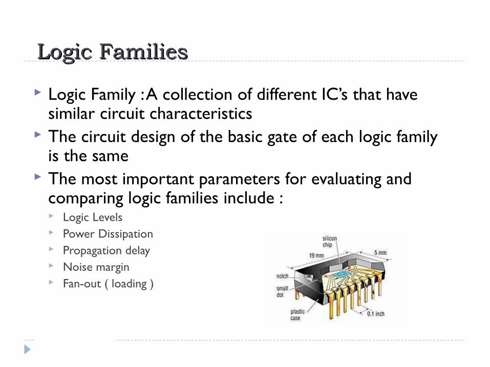
Logic FamiliesLogic Families
Logic Family : A collection of different IC’s that have similar circuit characteristics
The circuit design of the basic gate of each logic family is the same
The most important parameters for evaluating and comparing logic families include : Logic Levels Power Dissipation Propagation delay Noise margin Fan-out ( loading )

Example Logic FamiliesExample Logic Families
General comparison or three commonly available logic families.
the most important to understand
Implementing Logic CircuitsImplementing Logic Circuits
There are several varieties of transistors – the building blocks of logic gates – the most important are: BJT (bipolar junction transistors)
one of the first to be invented FET (field effect transistors)
especially Metal-Oxide Semiconductor types (MOSFET’s) MOSFET’s are of two types: NMOS and PMOS

Transistor Size ScalingTransistor Size Scaling
Performance improves as size is decreased: shorter switching time, lower power consumption.
2 orders of magnitude reduction in transistor size in 30 years.
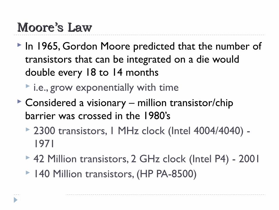
Moore’s LawMoore’s Law In 1965, Gordon Moore predicted that the number of
transistors that can be integrated on a die would double every 18 to 14 months i.e., grow exponentially with time
Considered a visionary – million transistor/chip barrier was crossed in the 1980’s 2300 transistors, 1 MHz clock (Intel 4004/4040) -
1971 42 Million transistors, 2 GHz clock (Intel P4) - 2001 140 Million transistors, (HP PA-8500)
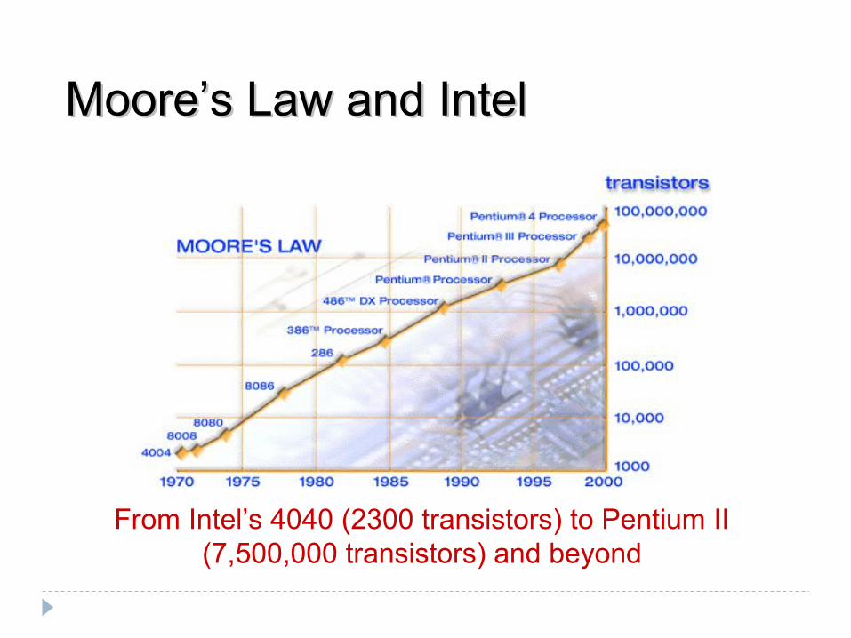
Moore’s Law and IntelMoore’s Law and Intel
From Intel’s 4040 (2300 transistors) to Pentium II (7,500,000 transistors) and beyond
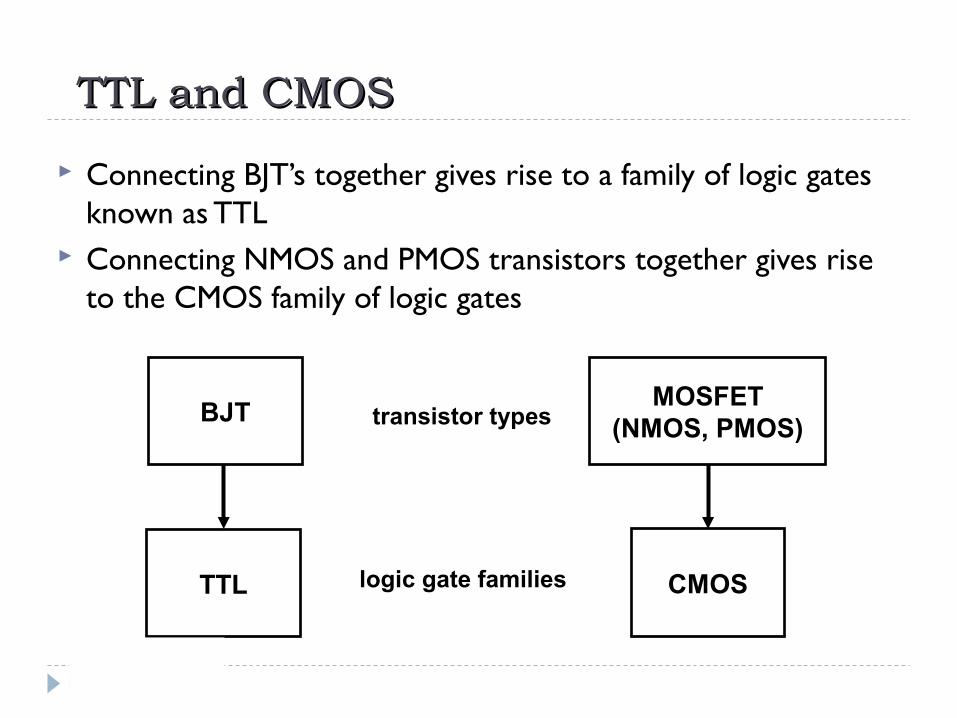
TTL and CMOSTTL and CMOS
Connecting BJT’s together gives rise to a family of logic gates known as TTL
Connecting NMOS and PMOS transistors together gives rise to the CMOS family of logic gates
BJTMOSFET
(NMOS, PMOS)
TTL CMOS
transistor types
logic gate families
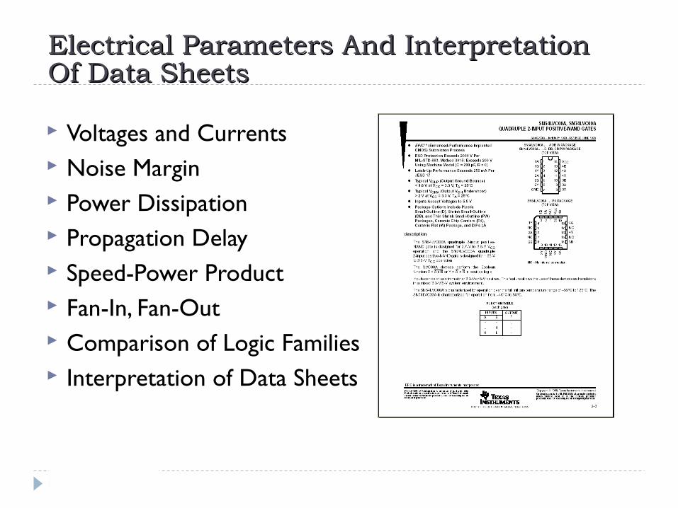
Electrical Parameters And Interpretation Electrical Parameters And Interpretation Of Data SheetsOf Data Sheets
Voltages and Currents Noise Margin Power Dissipation Propagation Delay Speed-Power Product Fan-In, Fan-Out Comparison of Logic Families Interpretation of Data Sheets
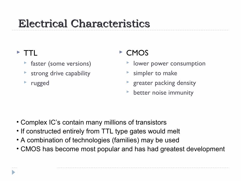
Electrical CharacteristicsElectrical Characteristics
TTL faster (some versions) strong drive capability rugged
CMOS lower power consumption simpler to make greater packing density better noise immunity
• Complex IC’s contain many millions of transistors• If constructed entirely from TTL type gates would melt• A combination of technologies (families) may be used• CMOS has become most popular and has had greatest development
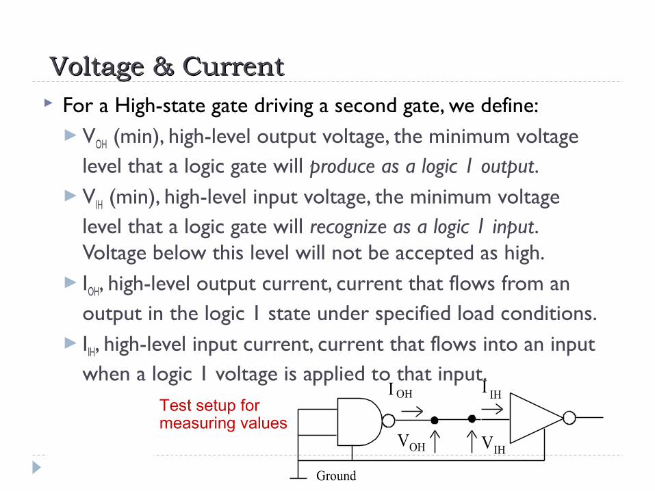
Voltage & CurrentVoltage & Current For a High-state gate driving a second gate, we define:
VOH (min), high-level output voltage, the minimum voltage level that a logic gate will produce as a logic 1 output.
VIH (min), high-level input voltage, the minimum voltage level that a logic gate will recognize as a logic 1 input. Voltage below this level will not be accepted as high.
IOH, high-level output current, current that flows from an output in the logic 1 state under specified load conditions.
IIH, high-level input current, current that flows into an input when a logic 1 voltage is applied to that input.
Ground
VIHVOH
I OH I IHTest setup for measuring values
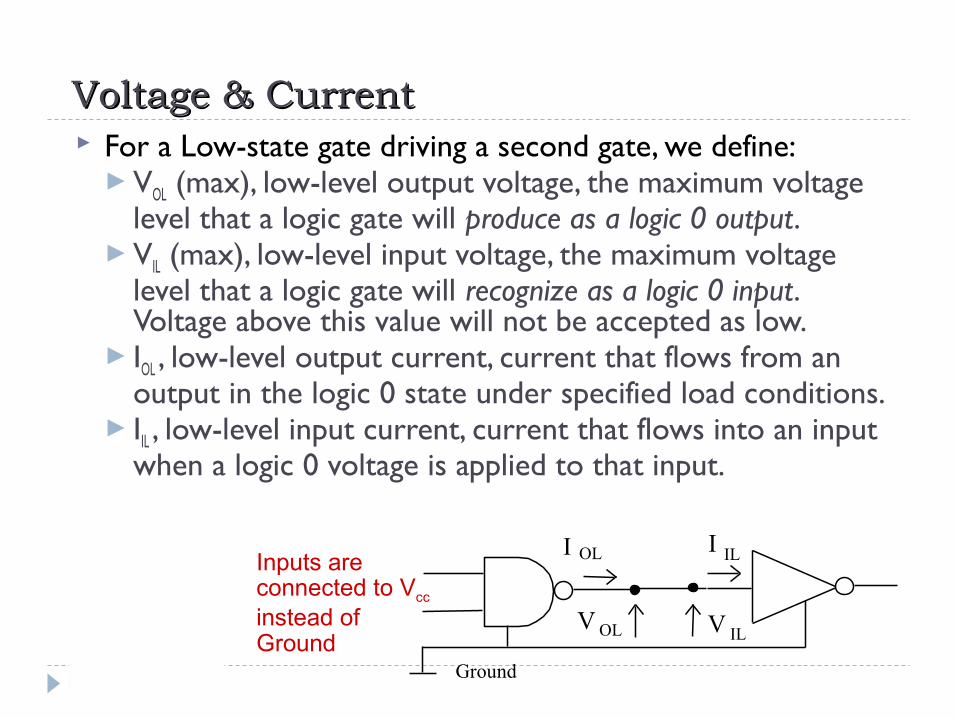
Voltage & CurrentVoltage & Current For a Low-state gate driving a second gate, we define:
VOL (max), low-level output voltage, the maximum voltage level that a logic gate will produce as a logic 0 output.
VIL (max), low-level input voltage, the maximum voltage level that a logic gate will recognize as a logic 0 input. Voltage above this value will not be accepted as low.
IOL , low-level output current, current that flows from an output in the logic 0 state under specified load conditions.
IIL , low-level input current, current that flows into an input when a logic 0 voltage is applied to that input.
Inputs are connected to Vcc instead of Ground
Ground
V ILV OL
I OL I IL
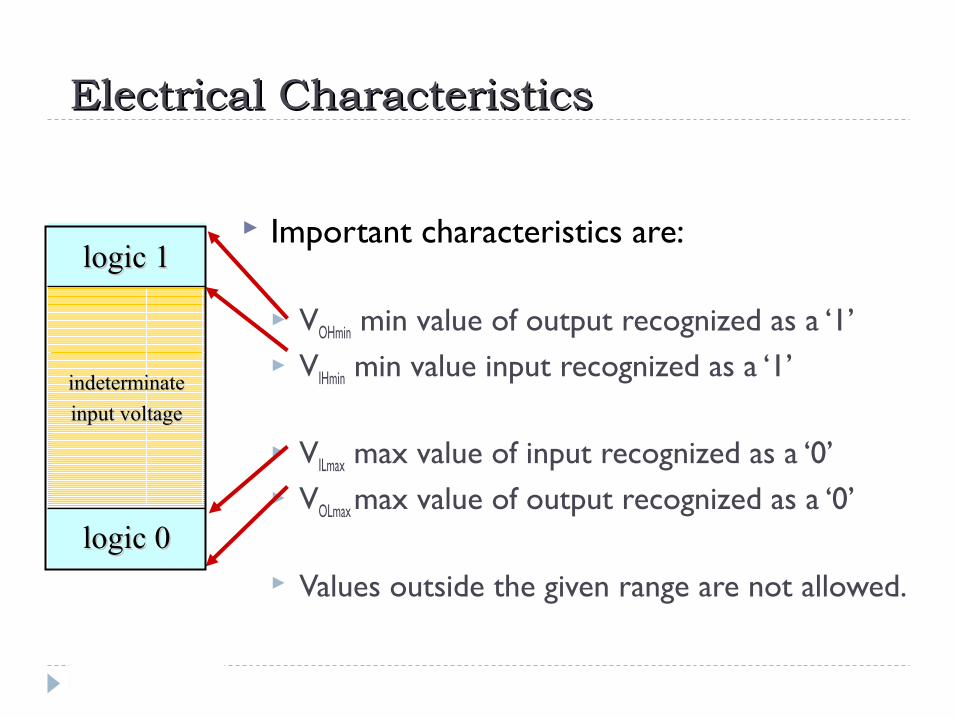
Electrical CharacteristicsElectrical Characteristics
Important characteristics are:
VOHmin min value of output recognized as a ‘1’ VIHmin min value input recognized as a ‘1’
VILmax max value of input recognized as a ‘0’ VOLmax max value of output recognized as a ‘0’
Values outside the given range are not allowed.logic 0logic 0
logic 1logic 1
indeterminateindeterminate
input voltageinput voltage
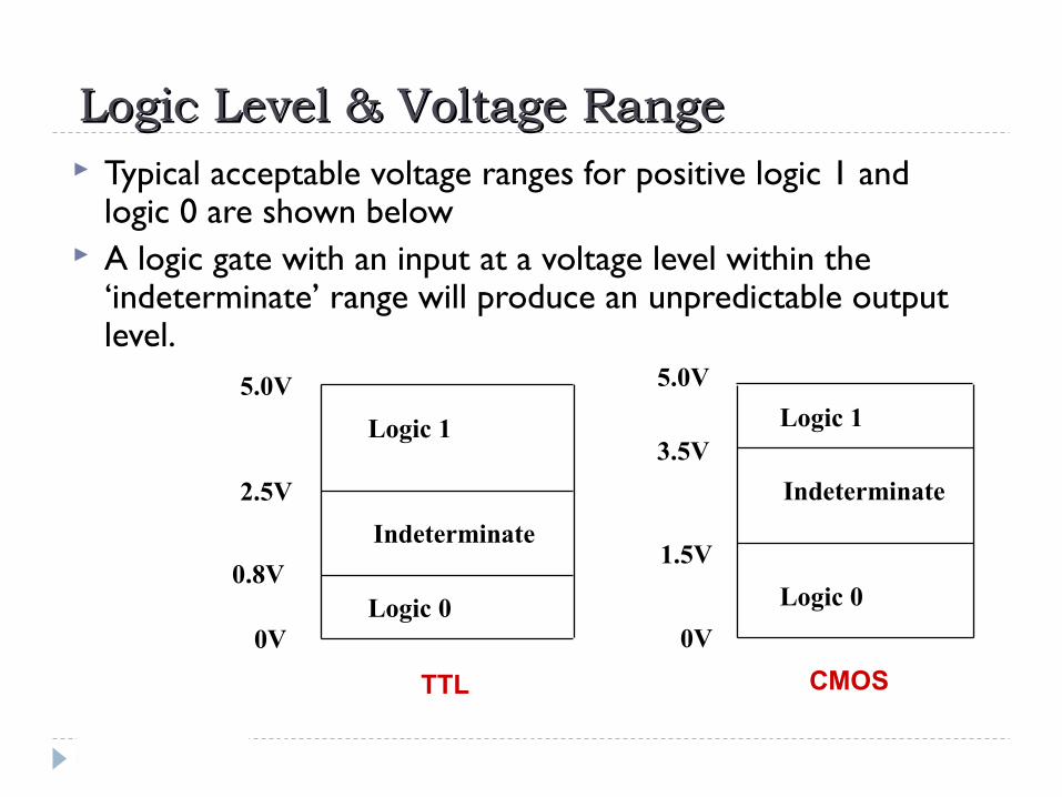
Logic Level & Voltage RangeLogic Level & Voltage Range Typical acceptable voltage ranges for positive logic 1 and
logic 0 are shown below A logic gate with an input at a voltage level within the
‘indeterminate’ range will produce an unpredictable output level.
Logic 1
Logic 0
5.0V
0V
2.5V
Indeterminate
0.8V
TTL
Logic 1
Logic 0
5.0V
Indeterminate
0V
1.5V
CMOS
3.5V
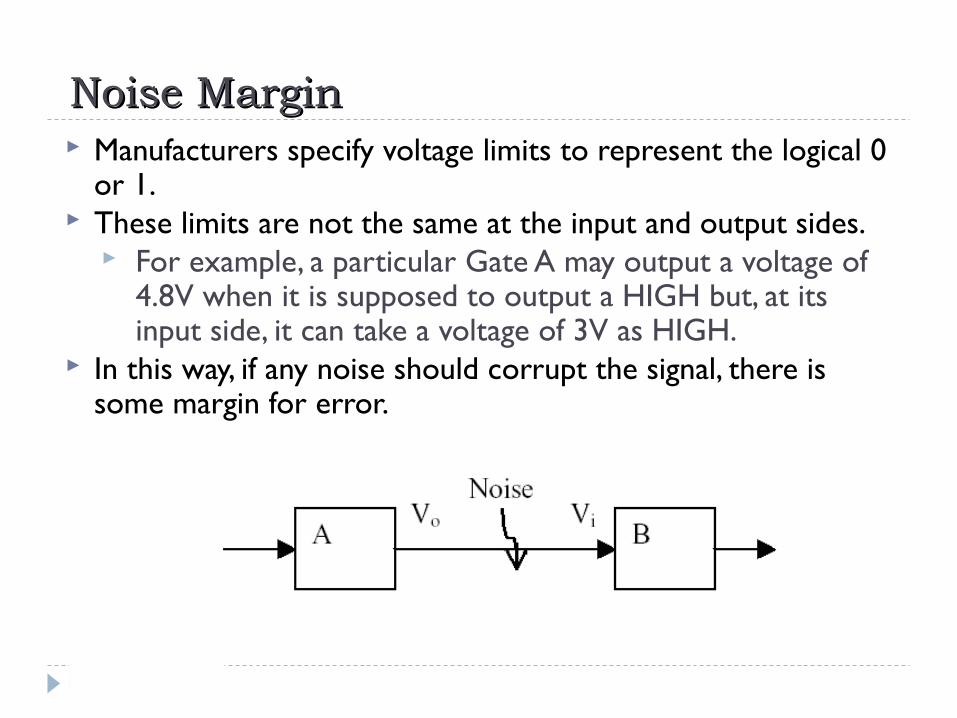
Noise MarginNoise Margin Manufacturers specify voltage limits to represent the logical 0
or 1. These limits are not the same at the input and output sides.
For example, a particular Gate A may output a voltage of 4.8V when it is supposed to output a HIGH but, at its input side, it can take a voltage of 3V as HIGH.
In this way, if any noise should corrupt the signal, there is some margin for error.
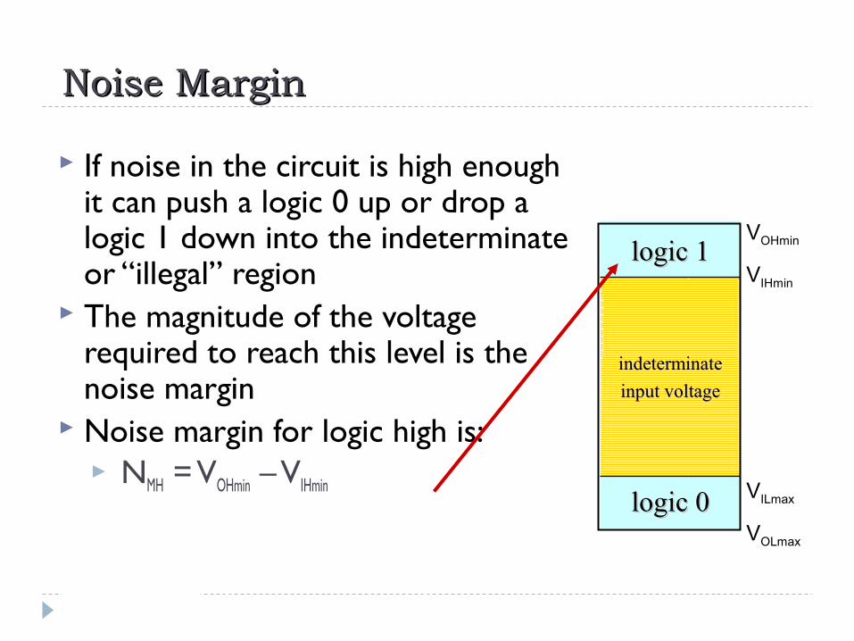
Noise MarginNoise Margin
If noise in the circuit is high enough it can push a logic 0 up or drop a logic 1 down into the indeterminate or “illegal” region
The magnitude of the voltage required to reach this level is the noise margin
Noise margin for logic high is: NMH = VOHmin – VIHmin
VOHmin
VIHmin
VILmax
VOLmax
logic 0logic 0
logic 1logic 1
indeterminateindeterminate
input voltageinput voltage
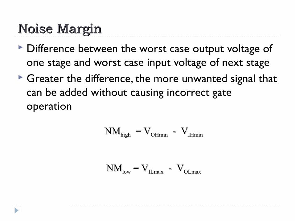
Noise MarginNoise Margin Difference between the worst case output voltage of
one stage and worst case input voltage of next stage Greater the difference, the more unwanted signal that
can be added without causing incorrect gate operation
NMNMhighhigh = V = VOHminOHmin - V - VIHminIHmin
NMNMlowlow = V = VILmaxILmax - V - VOLmaxOLmax
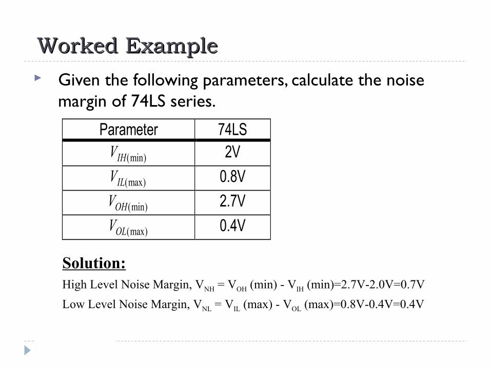
Worked ExampleWorked Example Given the following parameters, calculate the noise
margin of 74LS series.
Parameter 74LSVIH(min) 2V
VIL(max) 0.8V
VOH(min) 2.7V
VOL(max) 0.4V
Solution:High Level Noise Margin, VNH = VOH (min) - VIH (min)=2.7V-2.0V=0.7V
Low Level Noise Margin, VNL = VIL (max) - VOL (max)=0.8V-0.4V=0.4V

Noise Margin & Noise ImmunityNoise Margin & Noise Immunity Noise immunity of a logic circuit refers to the
circuit’s ability to tolerate noise voltages on its inputs.
A quantitative measure of noise immunity is called noise margin
High Level Noise Margin, VNH = VOH (min) - VIH (min) Low Level Noise Margin, VNL = VIL (max) - VOL (max)
Logic 1
Logic 0Logic 0
Logic 1VOH (min)
VOL (max)
VIH (min)
VIL (max)
VNH
VNL
Output Voltage Ranges Input Voltage Ranges
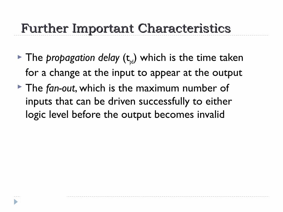
Further Important CharacteristicsFurther Important Characteristics
The propagation delay (tpd) which is the time taken for a change at the input to appear at the output
The fan-out, which is the maximum number of inputs that can be driven successfully to either logic level before the output becomes invalid
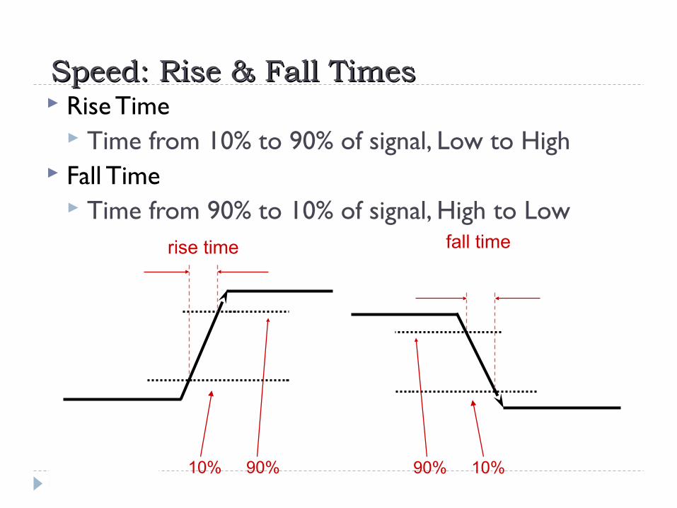
Speed: Rise & Fall TimesSpeed: Rise & Fall Times Rise Time
Time from 10% to 90% of signal, Low to High Fall Time
Time from 90% to 10% of signal, High to Lowrise time
10% 90% 90% 10%
fall time
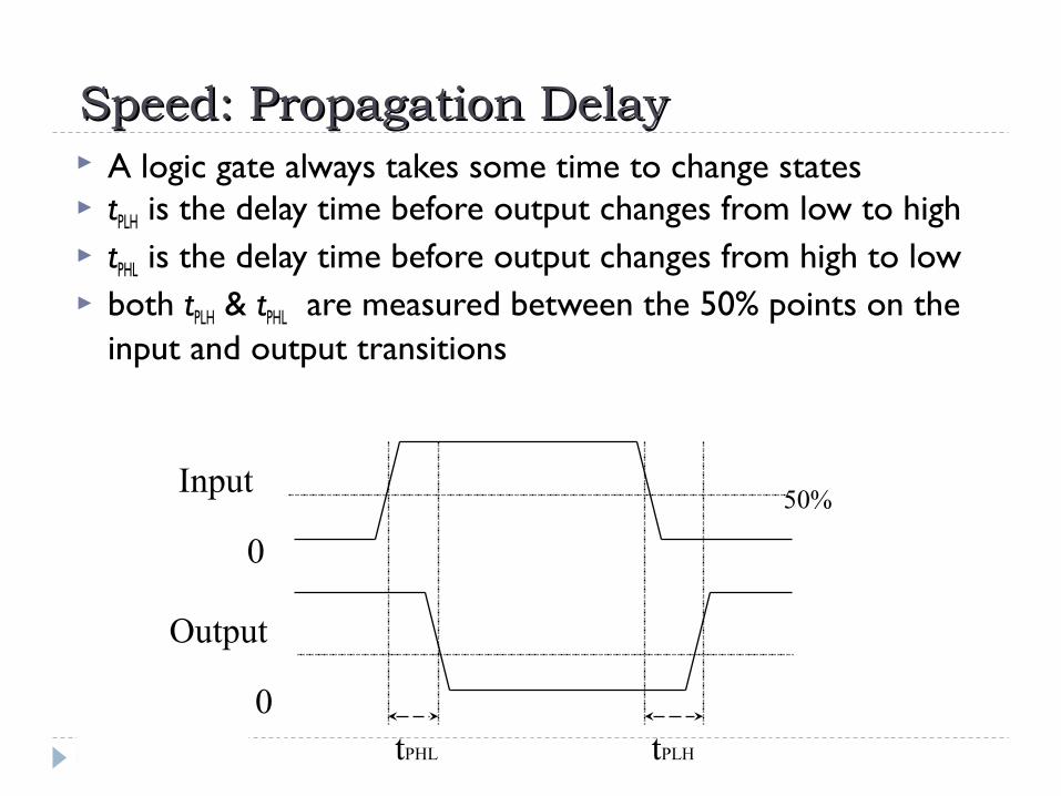
Speed: Propagation DelaySpeed: Propagation Delay A logic gate always takes some time to change states tPLH is the delay time before output changes from low to high tPHL is the delay time before output changes from high to low both tPLH & tPHL are measured between the 50% points on the
input and output transitions
50%Input
Output
0
0tPHL tPLH

Power DissipationPower Dissipation Static
I2R losses due to passive components, no input signal Dynamic
I2R losses due to charging and discharging capacitances through resistances, due to input signal

Speed-Power ProductSpeed-Power Product Speed (propagation delay) and power consumption are
the two most important performance parameters of a digital IC.
A simple means for measuring and comparing the overall performance of an IC family is the speed-power product (the smaller, the better).
For example, an IC has an average propagation delay of 10 ns an average power dissipation of 5 mW the speed-power product = (10 ns) x (5 mW) = 50 picoJoules (pJ)
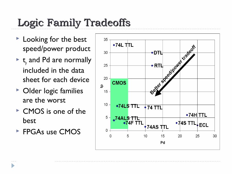
Logic Family TradeoffsLogic Family Tradeoffs
Looking for the best speed/power product
tp and Pd are normally included in the data sheet for each device
Older logic families are the worst
CMOS is one of the best
FPGAs use CMOS
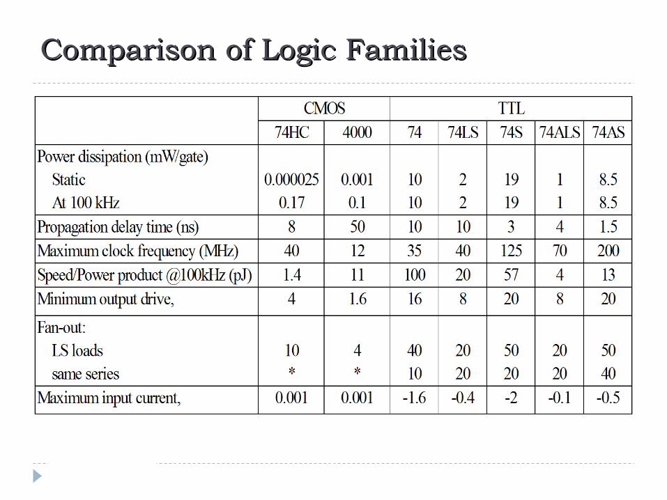
Comparison of Logic FamiliesComparison of Logic Families
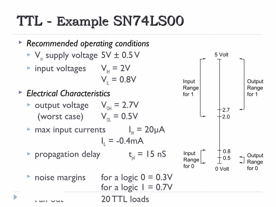
TTL - TTL - ExampleExample SN74LS00 SN74LS00
Recommended operating conditions Vcc supply voltage 5V ± 0.5 V input voltages VIH = 2V
VIL = 0.8V Electrical Characteristics
output voltage VOH = 2.7V (worst case) VOL = 0.5V
max input currents IIH = 20µAIIL = -0.4mA
propagation delay tpd = 15 nS
noise margins for a logic 0 = 0.3Vfor a logic 1 = 0.7V
Fan-out 20 TTL loads
5 Volt
0 Volt
0.80.5
2.02.7
InputRangefor 1
InputRangefor 0
OutputRangefor 0
OutputRangefor 1
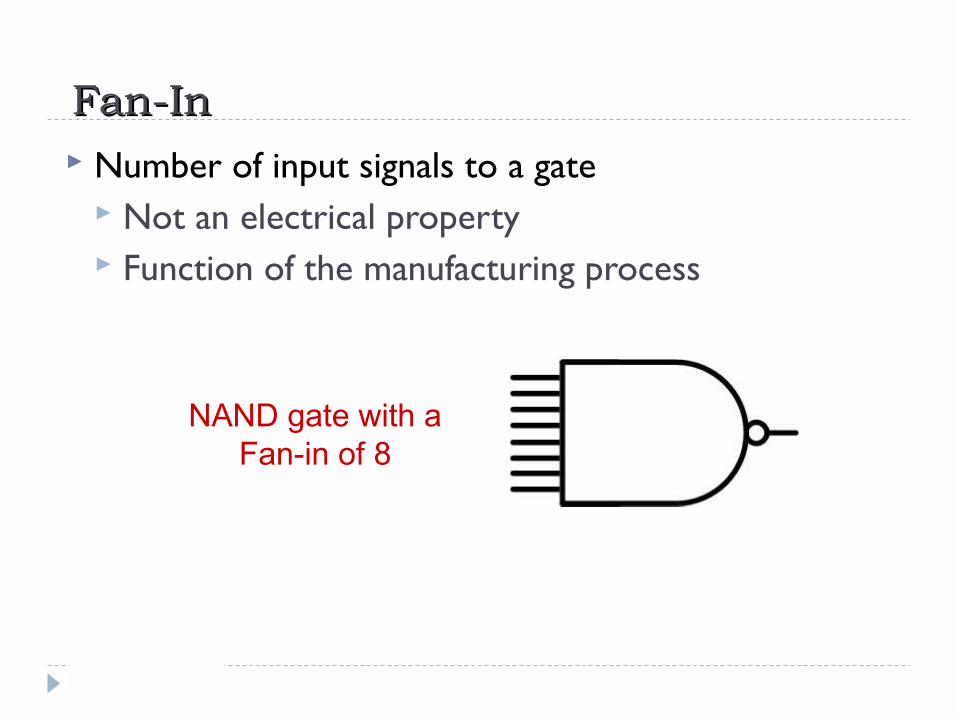
Fan-InFan-In Number of input signals to a gate
Not an electrical property Function of the manufacturing process
NAND gate with a Fan-in of 8
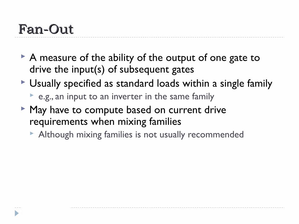
Fan-OutFan-Out
A measure of the ability of the output of one gate to drive the input(s) of subsequent gates
Usually specified as standard loads within a single family e.g., an input to an inverter in the same family
May have to compute based on current drive requirements when mixing families Although mixing families is not usually recommended
VOH
IIH
Low
VOL
IIL
High
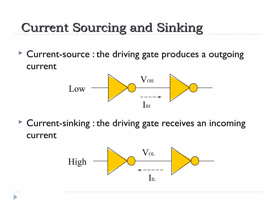
Current Sourcing and SinkingCurrent Sourcing and Sinking
Current-source : the driving gate produces a outgoing current
Current-sinking : the driving gate receives an incoming current
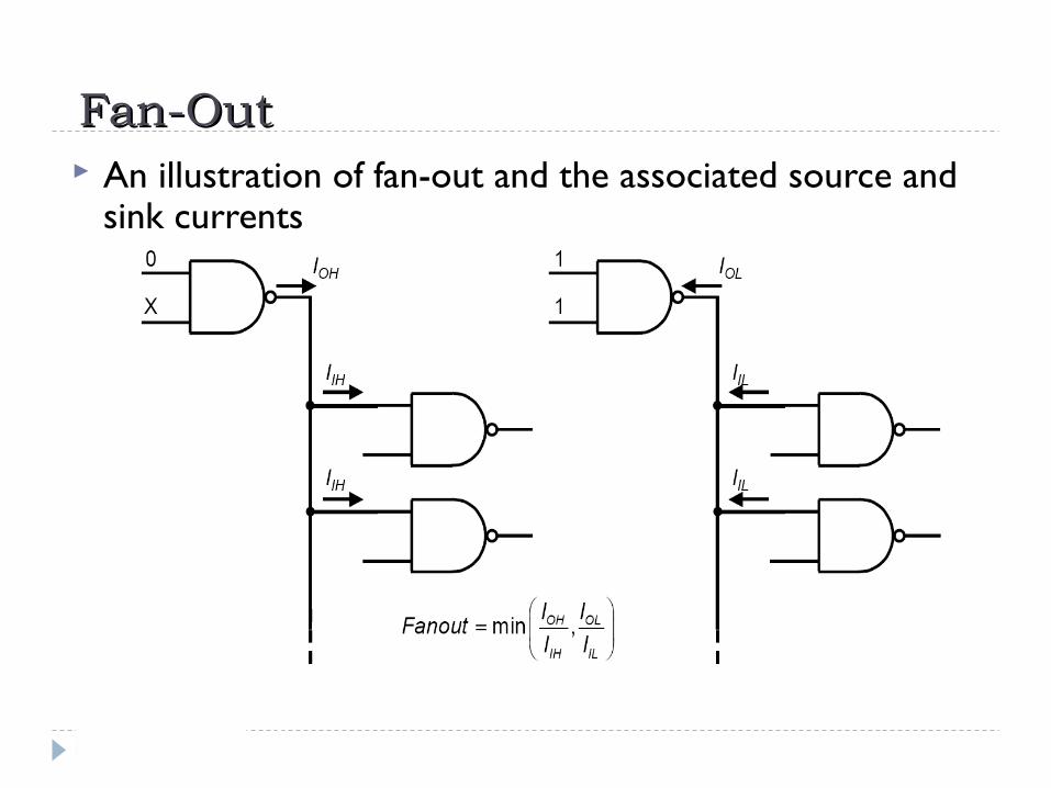
Fan-OutFan-Out An illustration of fan-out and the associated source and
sink currents
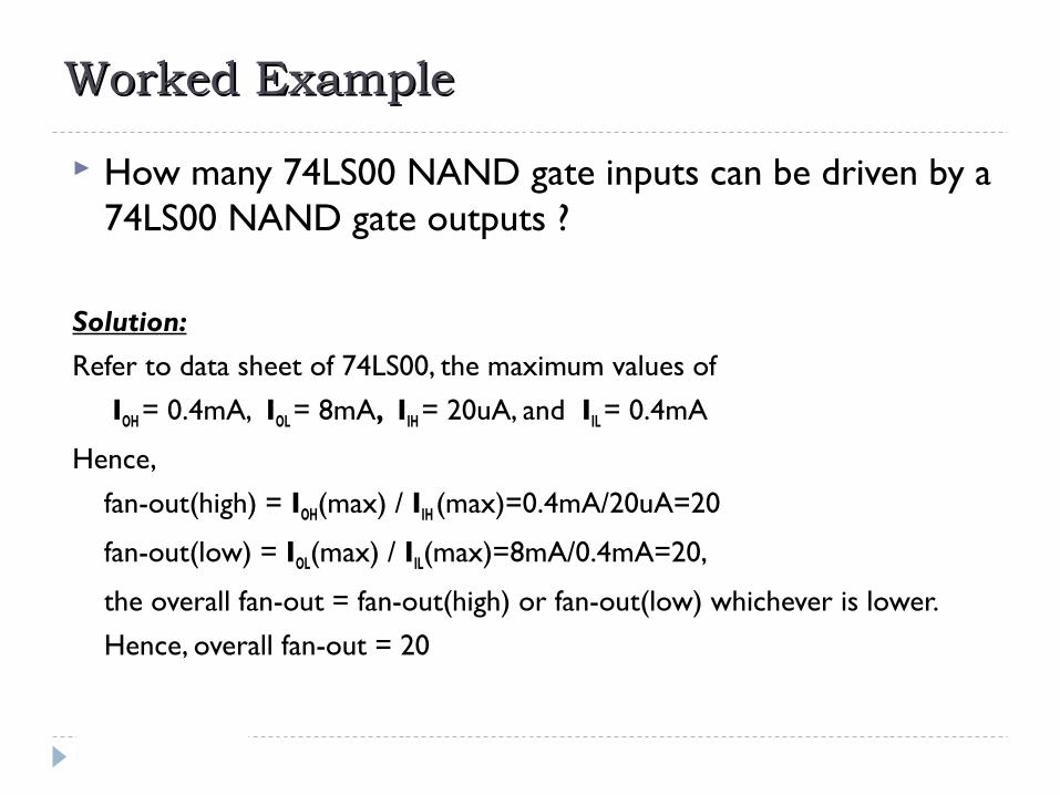
Worked ExampleWorked Example
How many 74LS00 NAND gate inputs can be driven by a 74LS00 NAND gate outputs ?
Solution:Refer to data sheet of 74LS00, the maximum values of
IOH = 0.4mA, IOL = 8mA, IIH = 20uA, and IIL = 0.4mA
Hence,
fan-out(high) = IOH(max) / IIH (max)=0.4mA/20uA=20
fan-out(low) = IOL(max) / IIL(max)=8mA/0.4mA=20,
the overall fan-out = fan-out(high) or fan-out(low) whichever is lower.
Hence, overall fan-out = 20
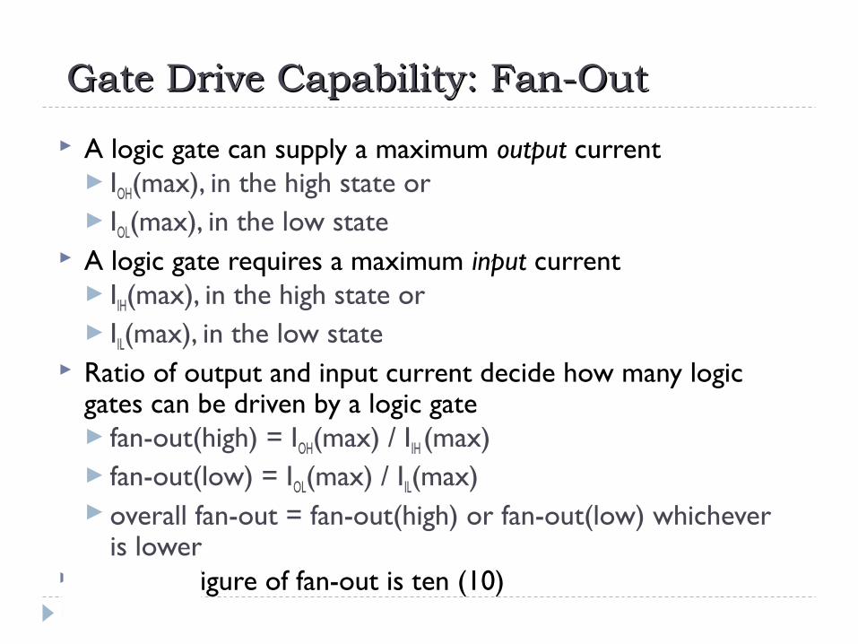
Gate Drive Capability: Fan-OutGate Drive Capability: Fan-Out
A logic gate can supply a maximum output current IOH(max), in the high state or IOL(max), in the low state
A logic gate requires a maximum input current IIH(max), in the high state or IIL(max), in the low state
Ratio of output and input current decide how many logic gates can be driven by a logic gate fan-out(high) = IOH(max) / IIH (max) fan-out(low) = IOL(max) / IIL(max) overall fan-out = fan-out(high) or fan-out(low) whichever
is lower A typical figure of fan-out is ten (10)
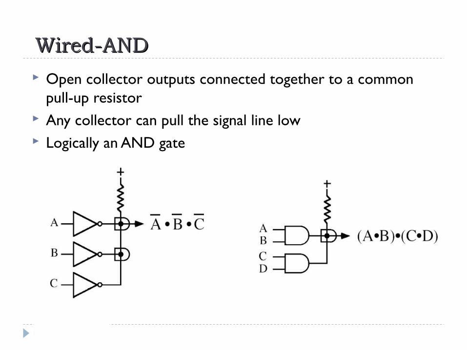
Wired-ANDWired-AND
Open collector outputs connected together to a common pull-up resistor
Any collector can pull the signal line low Logically an AND gate
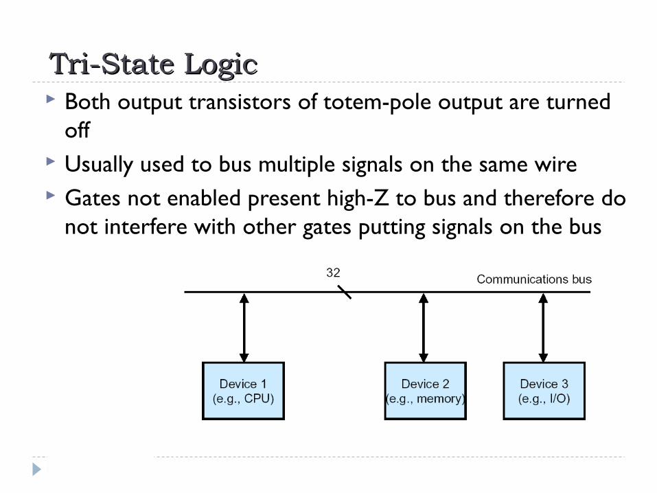
Tri-State LogicTri-State Logic Both output transistors of totem-pole output are turned
off Usually used to bus multiple signals on the same wire Gates not enabled present high-Z to bus and therefore do
not interfere with other gates putting signals on the bus
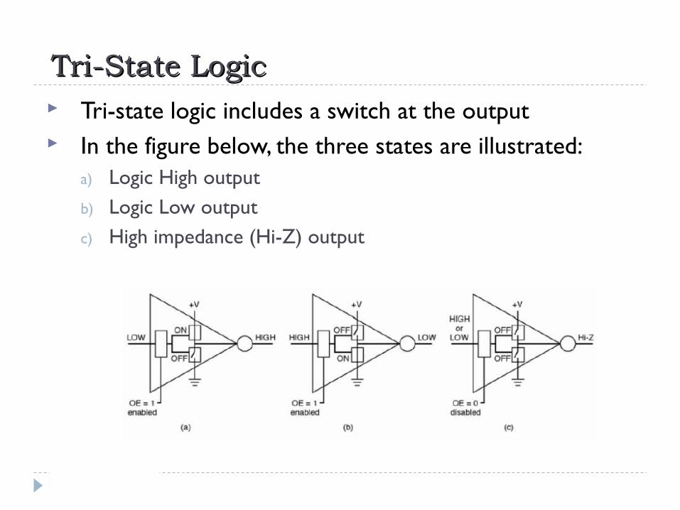
Tri-State LogicTri-State Logic Tri-state logic includes a switch at the output In the figure below, the three states are illustrated:
a) Logic High outputb) Logic Low outputc) High impedance (Hi-Z) output
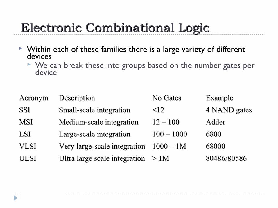
Electronic Combinational LogicElectronic Combinational Logic
Within each of these families there is a large variety of different devices We can break these into groups based on the number gates per
device
AcronymAcronym DescriptionDescription No GatesNo Gates ExampleExample
SSISSI Small-scale integrationSmall-scale integration <12<12 4 NAND gates4 NAND gates
MSIMSI Medium-scale integrationMedium-scale integration 12 – 10012 – 100 AdderAdder
LSILSI Large-scale integrationLarge-scale integration 100 – 1000100 – 1000 68006800
VLSIVLSI Very large-scale integrationVery large-scale integration 1000 – 1M1000 – 1M 6800068000
ULSIULSI Ultra large scale integrationUltra large scale integration > 1M> 1M 80486/8058680486/80586
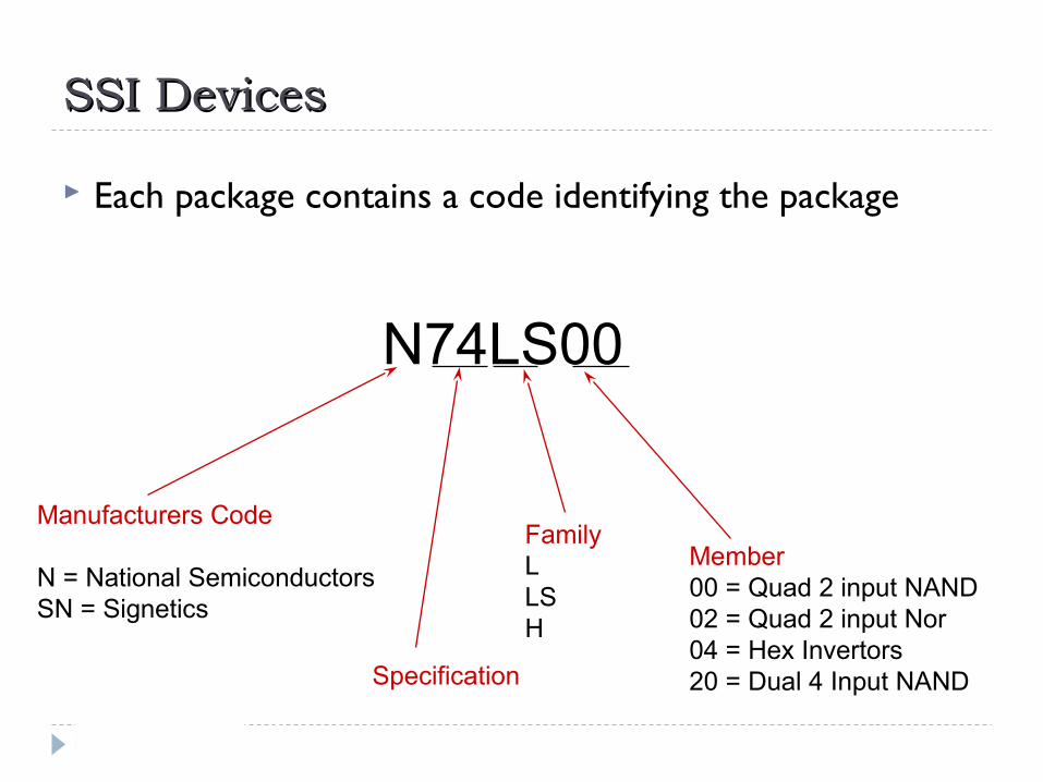
SSI DevicesSSI Devices
Each package contains a code identifying the package
N74LS00
Manufacturers Code
N = National SemiconductorsSN = Signetics
Specification
FamilyLLSH
Member00 = Quad 2 input NAND02 = Quad 2 input Nor04 = Hex Invertors20 = Dual 4 Input NAND
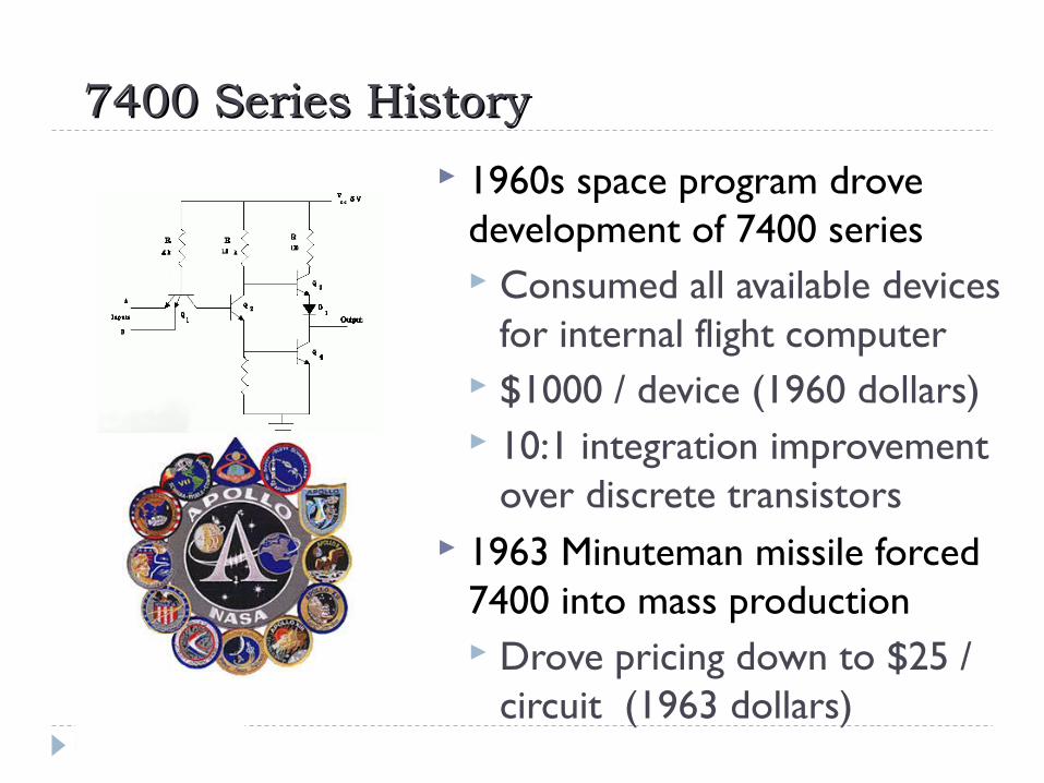
7400 Series History7400 Series History
1960s space program drove development of 7400 series Consumed all available devices
for internal flight computer $1000 / device (1960 dollars) 10:1 integration improvement
over discrete transistors 1963 Minuteman missile forced
7400 into mass production Drove pricing down to $25 /
circuit (1963 dollars)
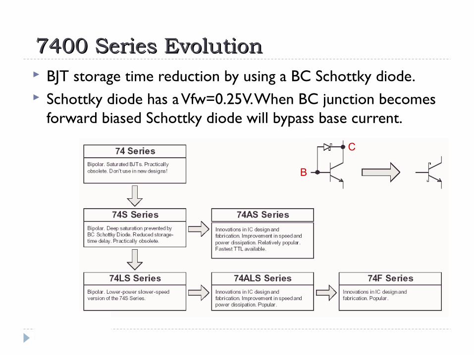
7400 Series Evolution7400 Series Evolution BJT storage time reduction by using a BC Schottky diode. Schottky diode has a Vfw=0.25V. When BC junction becomes
forward biased Schottky diode will bypass base current.
B
C
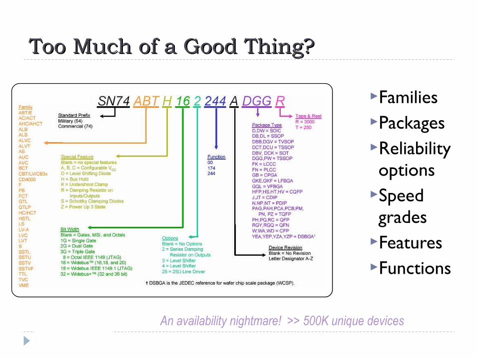
Too Much of a Good Thing?Too Much of a Good Thing?
FamiliesPackagesReliability options
Speed grades
FeaturesFunctions
An availability nightmare! >> 500K unique devices

The World of TTLThe World of TTL
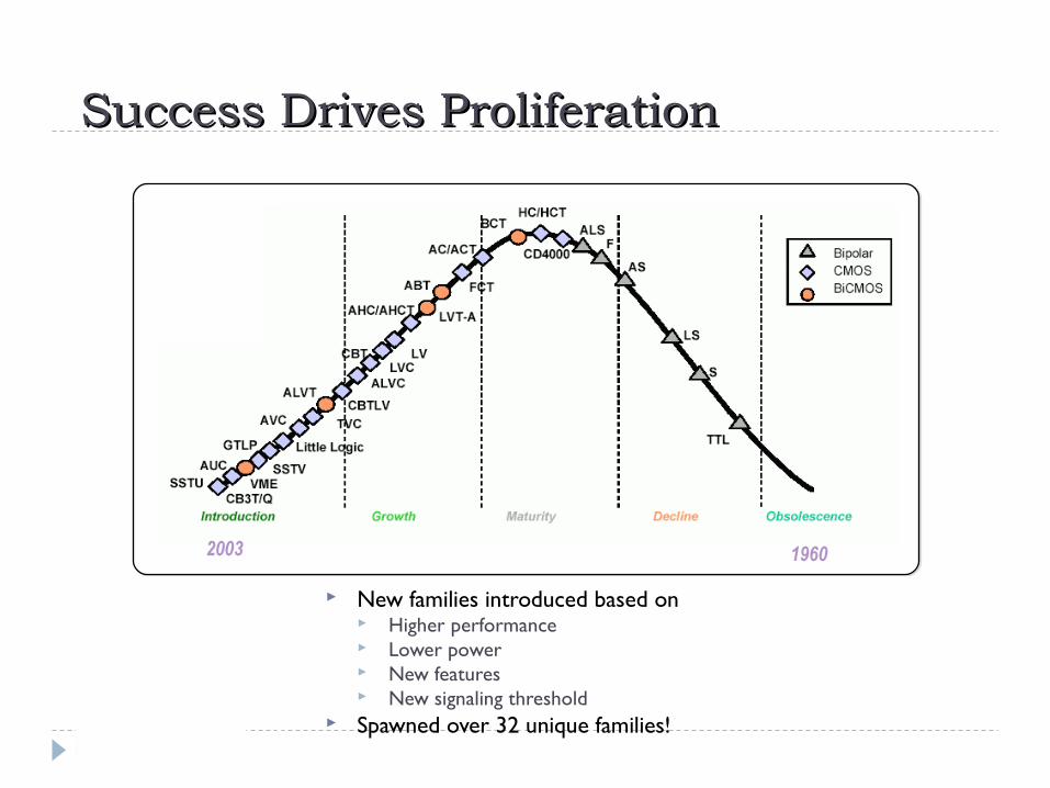
Success Drives ProliferationSuccess Drives Proliferation
New families introduced based on Higher performance Lower power New features New signaling threshold
Spawned over 32 unique families!
19602003
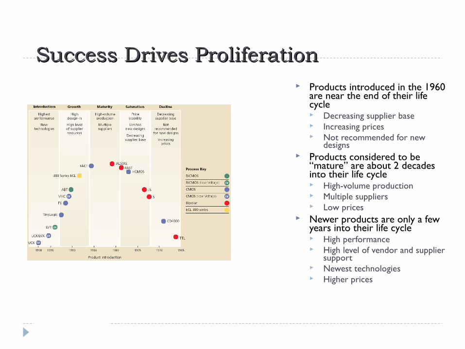
Success Drives ProliferationSuccess Drives Proliferation Products introduced in the 1960
are near the end of their life cycle Decreasing supplier base Increasing prices Not recommended for new
designs Products considered to be
“mature” are about 2 decades into their life cycle High-volume production Multiple suppliers Low prices
Newer products are only a few years into their life cycle High performance High level of vendor and supplier
support Newest technologies Higher prices
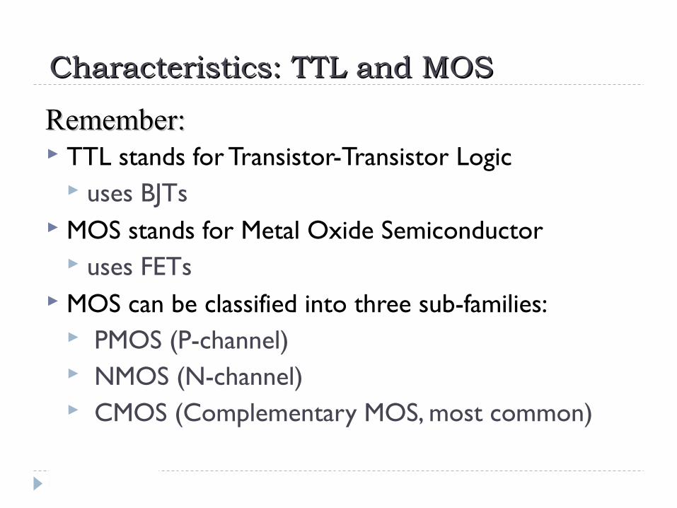
Characteristics: TTL and MOSCharacteristics: TTL and MOS
TTL stands for Transistor-Transistor Logic uses BJTs
MOS stands for Metal Oxide Semiconductor uses FETs
MOS can be classified into three sub-families: PMOS (P-channel) NMOS (N-channel) CMOS (Complementary MOS, most common)
Remember:Remember:
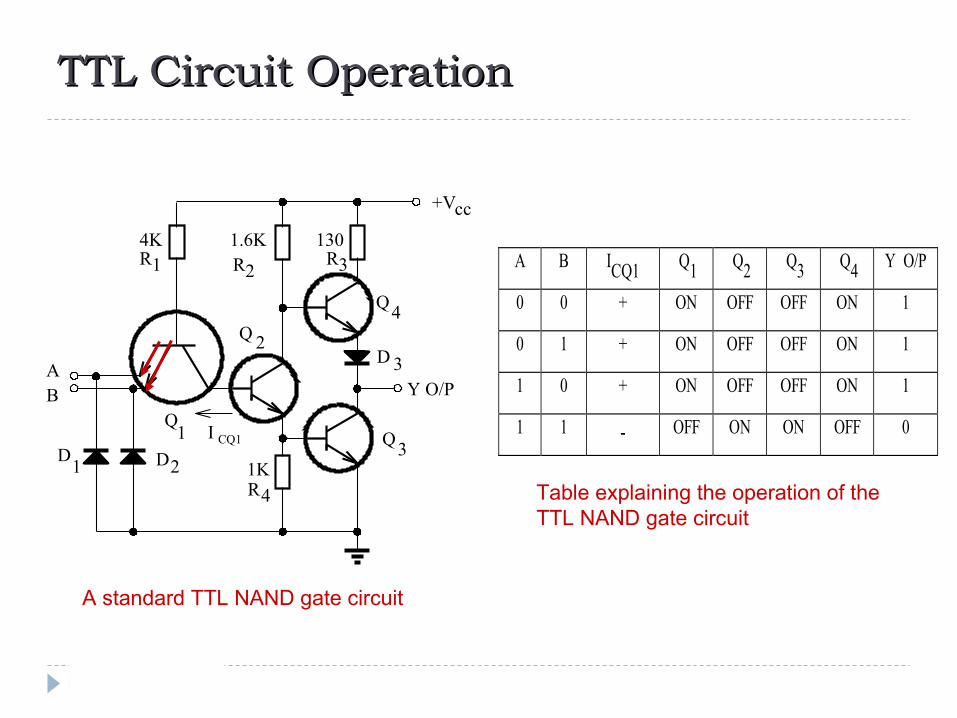
TTL Circuit OperationTTL Circuit Operation
AB Y O/P
+Vcc
Q1
Q 2
Q3
Q4
4K 1.6K 130R1 R2
R3
R4
1K
I CQ1
D 3
D1 D2
A B ICQ1 Q1 Q2 Q3 Q4 Y O/P
0 0 + ON OFF OFF ON 1
0 1 + ON OFF OFF ON 1
1 0 + ON OFF OFF ON 1
1 1 - OFF ON ON OFF 0
A standard TTL NAND gate circuit
Table explaining the operation of the TTL NAND gate circuit
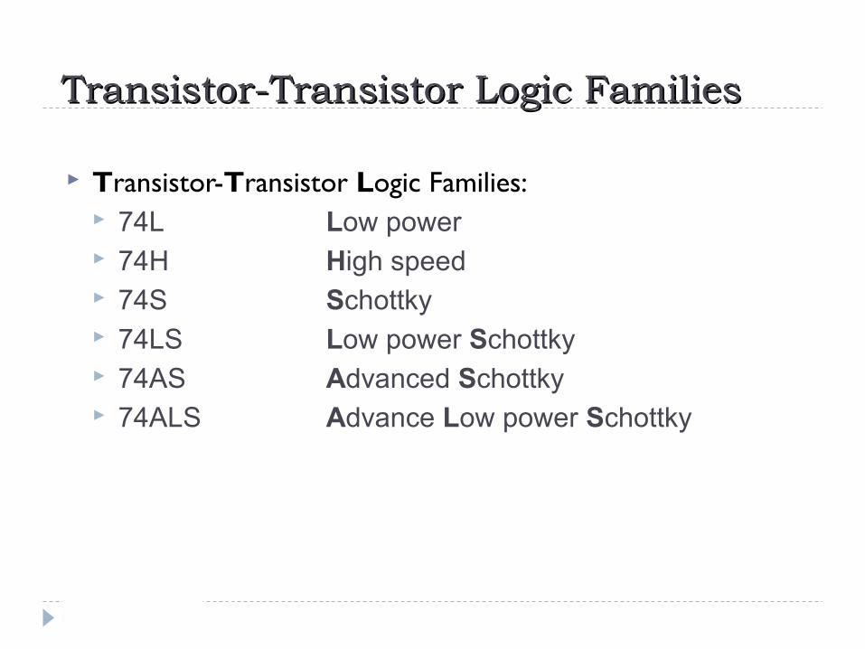
Transistor-Transistor Logic FamiliesTransistor-Transistor Logic Families
Transistor-Transistor Logic Families: 74L Low power 74H High speed 74S Schottky 74LS Low power Schottky 74AS Advanced Schottky 74ALS Advance Low power Schottky
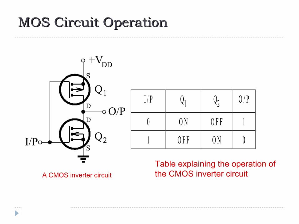
MOS Circuit OperationMOS Circuit Operation
+VDD
O/P
I/P
S
D
D
S
Q
Q
1
2
I / P Q1 Q2 O / P
0 O N O F F 1
1 O F F O N 0
Table explaining the operation of the CMOS inverter circuitA CMOS inverter circuit

CMOS Logic FamiliesCMOS Logic Families
CMOS Logic Families 40xx/45xx Metal-gate CMOS 74C TTL-compatible CMOS 74HC High speed CMOS 74ACT Advanced CMOS -TTL compatible
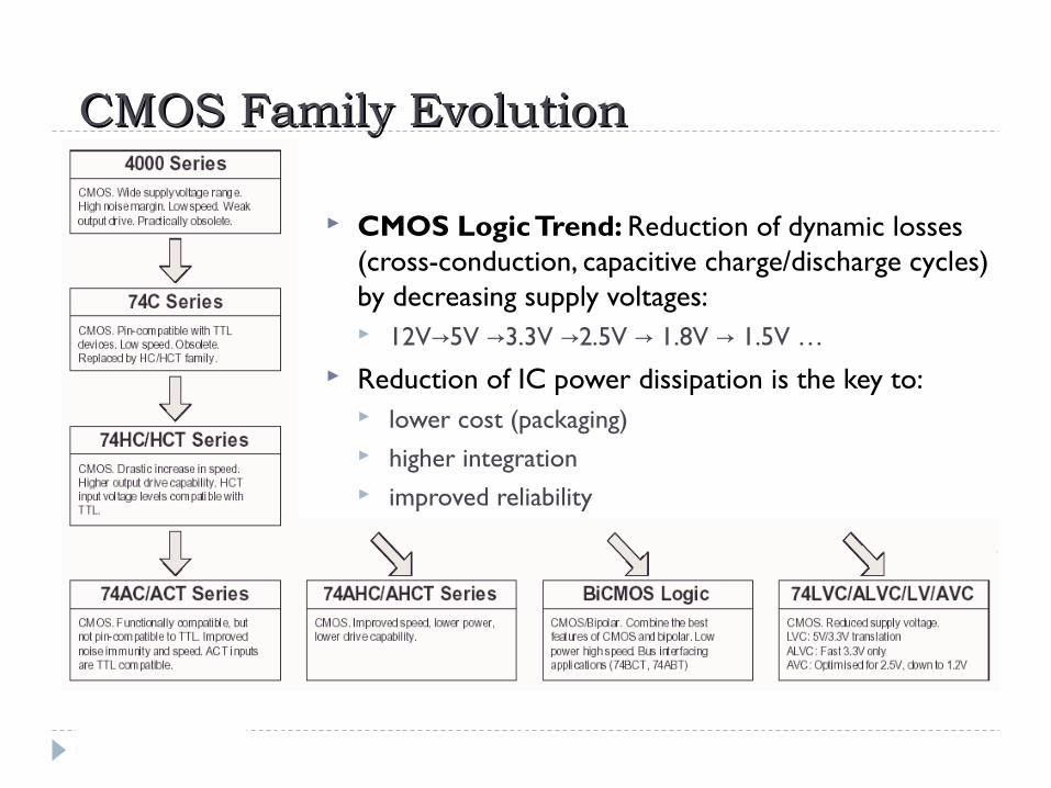
CMOS Family EvolutionCMOS Family Evolution
CMOS Logic Trend: Reduction of dynamic losses (cross-conduction, capacitive charge/discharge cycles) by decreasing supply voltages: 12V 5V 3.3V 2.5V 1.8V 1.5V …→ → → → →
Reduction of IC power dissipation is the key to: lower cost (packaging) higher integration improved reliability
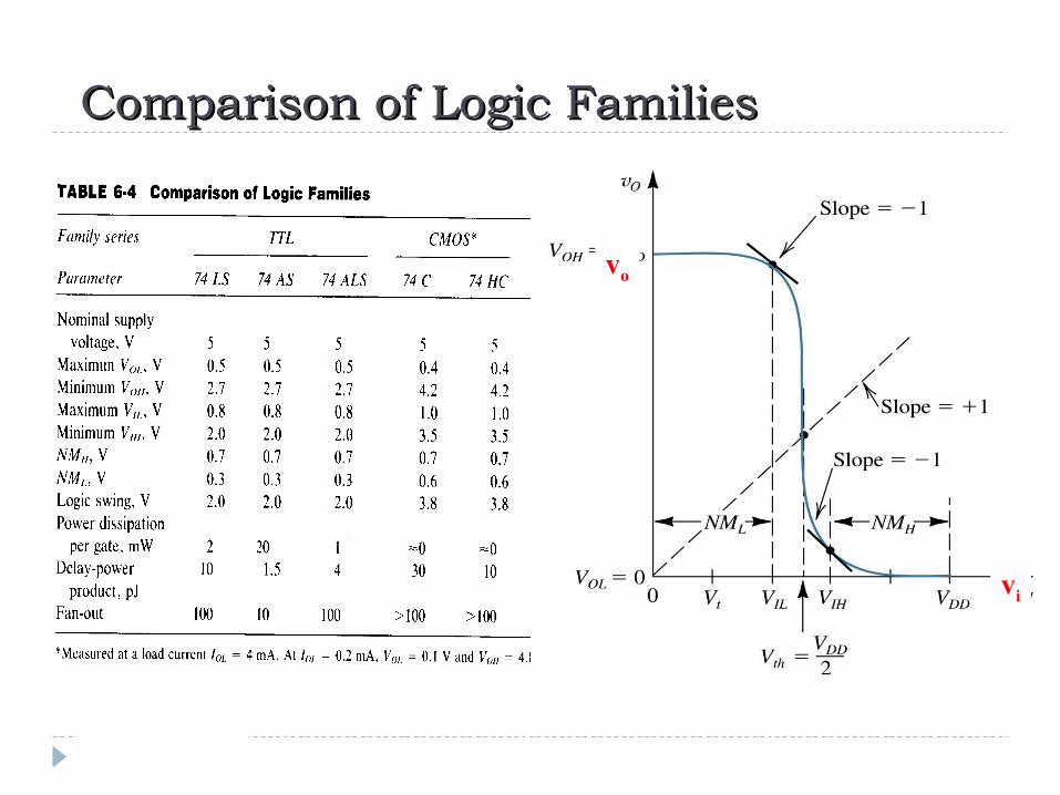
Comparison of Logic FamiliesComparison of Logic Families
vi
vo

Comparison Logic FamiliesComparison Logic Families
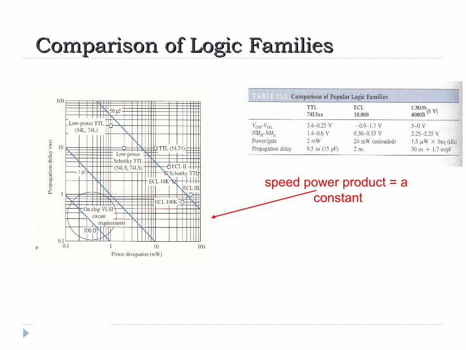
Comparison of Logic FamiliesComparison of Logic Families
speed power product = a constant
References Digital Logic and Computer Design – M. Morris Mano –
Pearson Fundamentals of Digital Circuits – A. Anand Kumar – PHI Digital Electronics - Gothmen - PHI Digital Electronics Principles - Malvino & Leech - MGH Digital fundamentals - Thomes L.Floyd and Jain - Pearson Modern Digital Electronics - R.P. Jain - TMH Digital Electronics -Tokneinh - MGH
Web References hyperphysics.phy-astr.gsu.edu/hbase/electronic/logfam.html is.iiita.ac.in/study/Digital%20Systems%20Design/KBab9Martarizal.pdf
nptel.ac.in/courses/106108099//Digital%20Systems.pdf www.owlnet.rice.edu/~dodds/Files331/digi_notes.pdf