axiem em simulation/verification of a cadence allegro pcb
TRANSCRIPT
80 hf-praxis 1/2018
RF & Wireless
This application example outlines
the electromagnetic (EM) simulation and verification flow that
exists between Cadence Allegro printed circuit
board (PCB) design software and NI AWR Design Environment,
specifically Microwave Office circuit design
and AXIEM EM analysis software, for a simple PCB design.
The PCB consisted of a transmission line, two
discontinuities, and ground via arrays.
Step-by-step instructions follow that explain how to first export a PCB design created within the Cadence Allegro PCB editor via an IPC2581 compatible file and then how to import the IPC2581 file into NI AWR Design Envi-ronment through its PCB import wizard.
Following the export/import steps, the creation of an EM simulation structure is shown and the tradeoffs between design complexity and simulation time are discussed. Lastly, an intro-duction to basic EM port confi-guration and simulation settings is provided and a comparison of the AXIEM EM simula-
tion against measured results is shown.
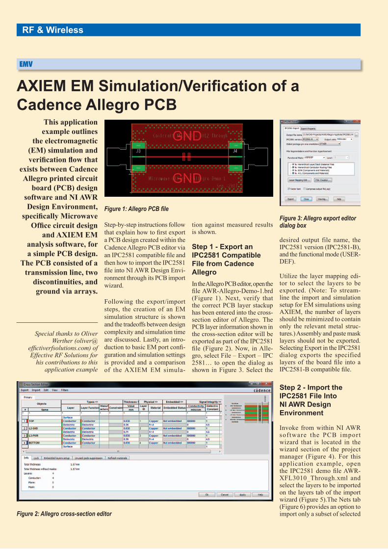
Step 1 - Export an IPC2581 Compatible File from Cadence AllegroIn the Allegro PCB editor, open the file AWR-Allegro-Demo-1.brd (Figure 1). Next, verify that the correct PCB layer stackup has been entered into the cross-section editor of Allegro. The PCB layer information shown in the cross-section editor will be exported as part of the IPC2581 file (Figure 2). Now, in Alle-gro, select File – Export – IPC 2581… to open the dialog as shown in Figure 3. Select the
desired output file name, the IPC2581 version (IPC2581-B), and the functional mode (USER-DEF).
Utilize the layer mapping edi-tor to select the layers to be exported. (Note: To stream-line the import and simulation setup for EM simulations using AXIEM, the number of layers should be minimized to contain only the relevant metal struc-tures.) Assembly and paste mask layers should not be exported. Selecting Export in the IPC2581 dialog exports the specified layers of the board file into a IPC2581-B compatible file.
Step 2 - Import the IPC2581 File Into NI AWR Design Environment
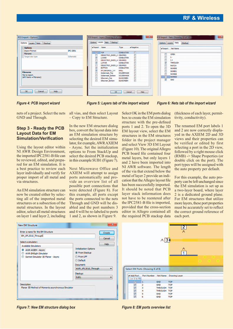
Invoke from within NI AWR software the PCB import wizard that is located in the wizard section of the project manager (Figure 4). For this application example, open the IPC2581 demo file AWR-XFL3010_Through.xml and select the layers to be imported on the layers tab of the import wizard (Figure 5).The Nets tab (Figure 6) provides an option to import only a subset of selected
Special thanks to Oliver Werther (oliver@
effictiverfsolutions.com) of Effective RF Solutions for
his contributions to this application example
AXIEM EM Simulation/Verification of a Cadence Allegro PCB
EMV
Figure 1: Allegro PCB file
Figure 2: Allegro cross-section editor
Figure 3: Allegro export editor dialog box
hf-praxis 1/2018 81
RF & Wireless
nets of a project. Select the nets GND and Through.
Step 3 - Ready the PCB Layout Data for EM Simulation/Verification
Using the layout editor within NI AWR Design Environment, the imported IPC2581-B file can be reviewed, edited, and prepa-red for an EM simulation. It is a best practice to review each layer individually and verify for proper import of all metal and via structures.
An EM simulation structure can now be created either by selec-ting all of the imported metal structures or a subsection of the metal structures. In the layout editor, select all metal structures on layer 1 and layer 2, including
all vias, and then select Layout – Copy to EM Structure.
In the new EM structure dialog box, convert the layout data into an EM simulation structure by selecting the desired EM simu-lator, for example, AWR AXIEM - Async. Set the initialization options to From StackUp and select the desired PCB stackup, in this example SUB1 (Figure 7).
Next Microwave Office and AXIEM will attempt to assign ports automatically and pro-vide an overview list of all possible port connections that were detected (Figure 8). For this example, all ports except the ports connected to the nets Through and GND will be dis-abled and the port numbers 3 and 4 will be re-labeled to ports 1 and 2, as shown in Figure 9.
Select OK in the EM ports dialog box to create the EM simulation structure with the pre-defined ports 1 and 2. To open the 3D EM layout view, select the EM structures in the EM structures folder in the project manager and select View 3D EM Layout (Figure 10). The original Allegro PCB board file contained four metal layers, but only layers 1 and 2 have been imported into NI AWR software. The length of the via that extend below the metal of layer 2 provide an indi-cation that the Allegro layout file has been successfully imported. It should be noted that PCB layer stack information does not have to be reentered after the IPC2581-B file is imported, provided that the cross-section editor in Allegro contained all the required PCB stackup data
(thickness of each layer, permit-tivity, conductivity).
The renamed EM port labels 1 and 2 are now correctly displa-yed in the AXIEM 2D and 3D views and their properties can be verified or edited by first selecting a port in the 2D view, followed by a right mouse click (RMB) -> Shape Properties (or double click on the port). The port types will be assigned with the auto property per default.
For this example, the auto pro-perty can be left unchanged since the EM simulation is set up as a two-layer board, where layer 2 is a dedicated ground plane. For EM structures that utilize more layers, these port properties must be accurately set to reflect the correct ground reference of each port.
Figure 4: PCB import wizard Figure 5: Layers tab of the import wizard Figure 6: Nets tab of the import wizard
Figure 7: New EM structure dialog box Figure 8: EM ports overview list

82 hf-praxis 1/2018
RF & Wireless
To generate the mesh for this EM structure, first specify the frequency range for the EM simulation. Set the frequency range to 1...6001 MHz with 100 MHz steps under the options sVetting of the EM
structure in the project manager (Figure 11). Select Mesh from the project manager (RMB on the desired EM structure), as shown in Figure 12. This will produce the result shown in Figure 13.
Mesh Complexity and EM Simulation Run Time
The meshed structure (Figure 13) can now be simulated but it will require a significant amount of memory and lengthy run times. While Cadence Allegro provides an elegant method to place via arrays around metal structures, traces, and transmission lines to improve shielding between nets and traces, this approach is not friendly to EM simulation/verification.
Vias are represented as circular tubes inside of EDA layout soft-ware. This representation can present unnecessarily long simu-lation run time for EM analysis tools. Thus, the defacto approach for EM software is to approxi-mate a via with a polygon.
The number and shape of the vias in the design could be reduced manually, a better approach is to invoke “rules” to simplify the layout and speed up the simula-tion without sacrificing accuracy.
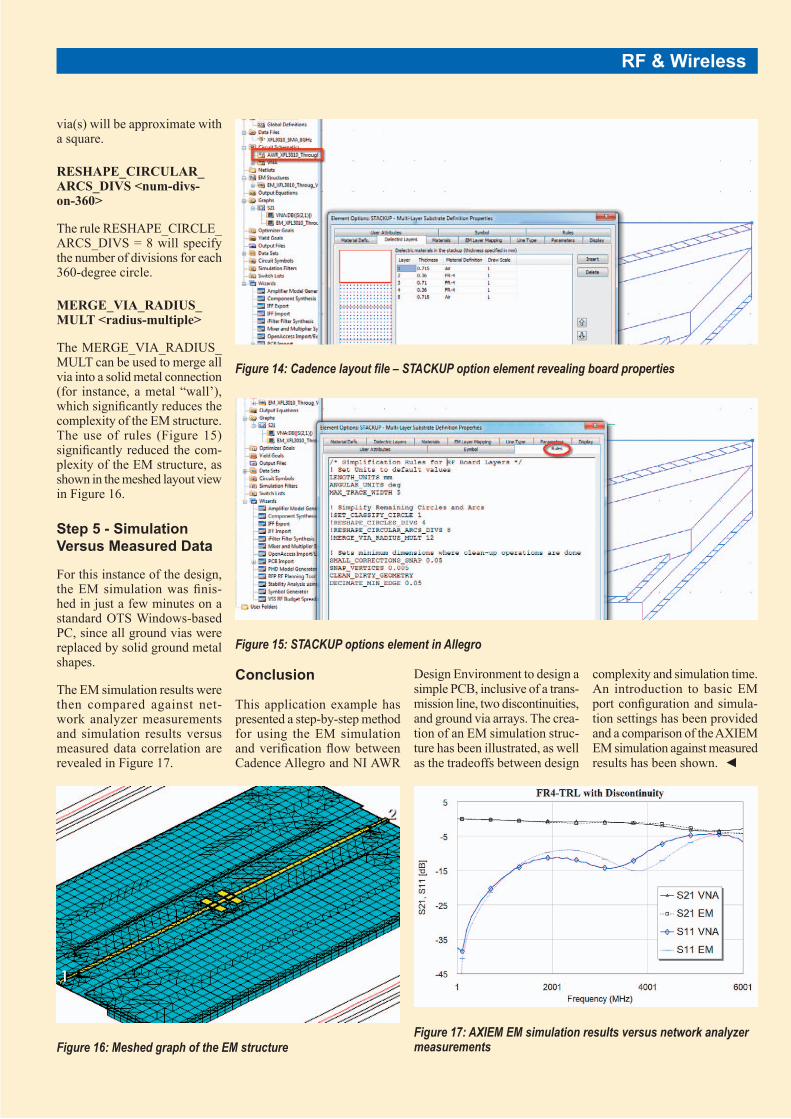
Step 4 - Using Import Rules to Simplify EM StructuresThe PCB import wizard that was used to import the IPC2581-compatible Allegro layout file automatically creates a sche-matic that contains a STACKUP option element (Figure 14) with the PCB properties contained within the Cadence Allegro cross-section editor.
The dielectric layer tab shows the thickness and material defi-nition of each layer, while the Materials Defs lists the detailed material properties that are used in this design.
The rules tab enables the user to specify additional rules that can be applied when the layout is copied to an EM structure within the NI AWR Design Environ-ment platform. A few example rules are shown below to provide a quick-reference starting point for simplifying the EM structure.
RESHAPE_CIRCLE_DIVS <number-of-edges>
The RESHAPE_CIRCLE_DIVS setting specifies the <number-of-edges> to be used to approximate all circles, either on a particular layer or all layers. For the rule RESHAPE_CIRCLE_DIVS = 4,
Figure 9: All ports except the ones connected to Through and GND are disabled. Ports 3 and 4 are relabelled to 1 and 2
Figure 10: 3D EM layout view
Figure 11: Options setting of the EM structure in the project manager
Figure 12: Project manager showing mesh selection
Figure 13: Mesh of the EM structure in AXIEM
hf-praxis 1/2018 83
RF & Wireless
via(s) will be approximate with a square.
RESHAPE_CIRCULAR_ARCS_DIVS <num-divs-on-360>
The rule RESHAPE_CIRCLE_ARCS_DIVS = 8 will specify the number of divisions for each 360-degree circle.
MERGE_VIA_RADIUS_MULT <radius-multiple>
The MERGE_VIA_RADIUS_MULT can be used to merge all via into a solid metal connection (for instance, a metal “wall’), which significantly reduces the complexity of the EM structure. The use of rules (Figure 15) significantly reduced the com-plexity of the EM structure, as shown in the meshed layout view in Figure 16.
Step 5 - Simulation Versus Measured Data
For this instance of the design, the EM simulation was finis-hed in just a few minutes on a standard OTS Windows-based PC, since all ground vias were replaced by solid ground metal shapes.
The EM simulation results were then compared against net-work analyzer measurements and simulation results versus measured data correlation are revealed in Figure 17.
Conclusion
This application example has presented a step-by-step method for using the EM simulation and verification flow between Cadence Allegro and NI AWR
Design Environment to design a simple PCB, inclusive of a trans-mission line, two discontinuities, and ground via arrays. The crea-tion of an EM simulation struc-ture has been illustrated, as well as the tradeoffs between design
complexity and simulation time. An introduction to basic EM port configuration and simula-tion settings has been provided and a comparison of the AXIEM EM simulation against measured results has been shown. ◄
Figure 14: Cadence layout file – STACKUP option element revealing board properties
Figure 15: STACKUP options element in Allegro
Figure 16: Meshed graph of the EM structureFigure 17: AXIEM EM simulation results versus network analyzer measurements