automotive packaging - · pdf fileautomotive packaging autonomous driving, clean & green...
TRANSCRIPT
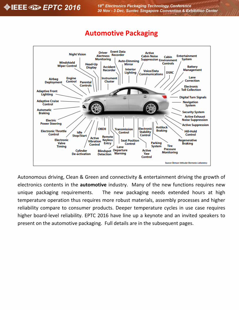
Automotive Packaging
Autonomous driving, Clean & Green and connectivity & entertainment driving the growth of
electronics contents in the automotive industry. Many of the new functions requires new
unique packaging requirements. The new packaging needs extended hours at high
temperature operation thus requires more robust materials, assembly processes and higher
reliability compare to consumer products. Deeper temperature cycles in use case requires
higher board-level reliability. EPTC 2016 have line up a keynote and an invited speakers to
present on the automotive packaging. Full details are in the subsequent pages.
KEYNOTE
Achieving Automotive Quality Excellence: Zero
Defect Performance - a Foundry’s Perspective
JAGADISH C.V.
SYSTEMS ON SILICON MANUFACTURING COMPANY (SSMC)
The automotive industry is well known for its high demand on safety, quality and reliability. Furthermore, the
electronic content of an automotive vehicle has been increasing steadily in the last two decades to achieve higher
system integration of new functions and capabilities. Hence the semiconductor chip, which is at the heart of its
electronic system, needs to be extremely low in defect (or zero defect) and high in reliability. Automotive
Semiconductor Manufacturers strive to meet the challenge of developing high quality fabrication processes to support
the expansion of automotive ICs of future markets.
This keynote presentation will outline a systematic approach to implementing automotive readiness in critical
fabrication processes that help to accelerate the supply chain towards automotive quality excellence. A 360 degree
foundry perspective in achieving the automotive quality goal will be presented. In addition, top must-do actions for
going beyond zero defect performance, moving from ppm to ppb level, meeting today and future automotive market,
will be shared.
Biography: Jagadish C.V.
Mr. Jagadish C.V. was appointed CEO of Systems on Silicon Manufacturing Company (SSMC), a joint venture of TSMC
and NXP in December 2006. Jagadish has vast experience in the business development arena and semiconductor
industry. He was a Director with FEI Company of USA before embarking his career with SSMC. Prior to his appointment
as CEO, Jagadish served as Vice President, Business Operations of SSMC. He is currently a member of the NXP’s
operations management team. Jagadish also serves as the Deputy Chairman of the Singapore National Quality Award
Governing Council and Power Quality Advisory Panel (PQAP) of Singapore since 2007. He is also the Vice Chairman of
SEMI, Singapore Regional Advisory Board (RAB) since 2010; and Deputy Chairman of the PUB Water Network Panel
since 2015. He is also a member of Singapore Semiconductor Industry Association (SSIA) Board of Advisors since 2011.
He holds a first class honors bachelor’s degree in Electronics & Communication from the National Institute of
Engineering Mysore, India; and completed the International Executive Program by INSEAD Management School,
France.
INVITED PRESENTATION
Package Miniaturization & Integration for Future
Automotive Applications
Andreas Fischer
ASIC Packaging Development
Robert Bosch GmbH
Technical Session: 2nd December 2016, 8:30hrs
Venue : MR333
Abstract Advanced driver assistance systems, automated driving features, and comprehensive vehicle connectivity are key selling features for current and future automobiles.The race of car manufacturers towards smart mobility is both, a major challenge and an opportunity for the automotive electronics industry.
Smart mobility requires highly integrated solutions with technology and packaging features and performance known from consumer electronics, but designed and approved for safety-relevant automotive applications under harsh conditions. Heterogeneously integrated packaging solutions will significantly increase technical complexity. At the same time automotive quality standards and lifetime requirements for the entire system have to be fulfilled, knowing that trends in automotive electronics will push the limits for certain applications to even higher levels than today.
Key capabilities to be successful are a profound knowledge of technology features, the related failure modes, and quantitative characterization of materials and interfaces. Those will be the basis for improved simulation-based engineering already in early design phases. Examples for that methodology are shown and an outlook towards possible improvements will be given.
Biography: Andreas Fischer
Andreas Fischer has studied physics at the University of Ulm, Germany, focusing on solid state and polymer physics.
After his master thesis on nuclear magnetic resonance and polymer dynamics he joined Bosch in 1990, starting as a
process development engineer for hybrid circuits and sensors. Then he moved to assembly & packaging as a project
manager for packaging development for ASICs. Currently he is senior manager for ASIC packaging development.
Requirement for Advanced-Packaging Technology of
Power Semiconductor Module in High Power Density
Converter for More Electric Transportation
Dr. Rejeki Simanjorang
Advanced Technology Center, Rolls-Royce Singapore Technical Session: 2nd December 2016, 13:40hrs
Venue : MR336
A recent trend in more electric technology for transportation system, such as in automotive, traction, and even in
aircraft has made power electronics technology become indispensable. In aircraft industry, more electric technology
will replace mechanical, hydraulic, and pneumatic system with electrical system that is more efficient, reliable, and
environmentally friendly. This is commonly known as More Electric Aircraft (MEA) technology. As a result, there is
increasing electric power demand in the aircraft. To satisfy such demand, power electronics converter that converts
and control electrical power is the key enabling technology. For this weight concerned application, the main
performance index of the power converters is their power density which determines how heavy and compact the
converters are.
To realize a high power density converter, the most straight-forward way will be by increasing the switching frequency
of the converter. By doing so, the size of passive components (capacitor and inductor) will reduce. Along with that,
thermal management of the converter should be taken care of to ensure the device operates within permissible
temperature range. High switching frequency of converter means driving the power semiconductor module (consists
of power semiconductor devices in a package) at high frequency. This can only be achieved by high speed switching
techniques to minimize the switching losses in the power module. To enable high speed switching there are two
important factors, i.e. the power devices and the packaging around it.
In recent years, wide band gap power devices such as Silicon Carbide and Gallium Nitride have entered the
commercial market. These power devices have the capability for high speed switching. Unfortunately, the currently
applied packaging technology does not allow full utilization of these wide band gap devices’ capability.
This presentation will elaborate the electrical performances of power module required for high speed switching in
high power density converter. Parasitic impedance in power module that originates from devices and packaging layout
will be discussed. Their effects to the power converters such as overshoot voltage, EMI issues, and switching loss will
be elaborated. Finally, advanced packaging technique to minimize these parasitic impedances will be presented.
Biography: Rejeki Simanjorang
Rejeki Simanjorang was born in Tanah Karo, Indonesia. He received his B.Sc., M.Eng. and Dr.Eng. degrees in Electrical
Engineering from University of Sumatera Utara (Indonesia, 1998), Bandung Institute of Technology (Indonesia, 2002)

and Osaka University (Japan, 2008) respectively. He was a researcher in National Institute of Advanced Industrial
Science and Technology (AIST) and R&D partnership for Future Power Electronic Technology (FUPET), Japan from 2008
to 2013. Currently, he is a technologist in Rolls-Royce Singapore and leading some collaboration research projects
between Rolls-Royce Singapore and external partners. His main research focuses are application of power electronic
converter in electrical system, design of high power density converter, and Electrical Health Monitoring (EHM) system
for power electronics.