automotive 12 v 200 w (20 a) bldc motor drive reference design
TRANSCRIPT

Motor driver
Motor feedback
Watchdog
Voltage regulator
Temperature sense
Position feedback
12 V
FETs
FETsFETs
Reverse battery
protection
Controller
1TIDUBP9–June 2016Submit Documentation Feedback
Copyright © 2016, Texas Instruments Incorporated
Automotive 12 V 200 W (20 A) BLDC Motor Drive Reference Design
TI DesignsAutomotive 12 V 200 W (20 A) BLDC Motor DriveReference Design
LaunchPad, Piccolo, Code Composer Studio, InstaSPIN-FOC, Insta-SPIN-MOTION are trademarks of Texas Instruments.Webench is a registered trademark of Texas Instruments.Diodes is a trademark of Diodes Inc.Nichicon is a trademark of Nichicon Corporation.Panasonic is a trademark of Panasonic Corporation.Rohm is a trademark of Rohm Co Ltd.ON Semi is a trademark of Semiconductor Components Industries, LLC.Vishay is a trademark of Vishay Precision Group, Inc.
TI DesignsThis TI Design is a 3-Phase Brushless DC Motor Drivedesigned to operate in 12-V automotive applications.The board is designed to drive motors in the 200-Wrange and can handle currents up to 20-A. The designincludes analog circuits working in conjunction with aC2000 LaunchPad™ to spin a 3-Phase BLDC motorwithout the need for position feedback from Hall Effectsensors or quadrature encoder. The board providesfiltering and protection against reverse-polarityconditions on the input power. On-board temperaturesense, voltage sense, and current sense provide a fullrange of diagnostic and fault-protection features.
Design Resources
TIDA-00901 Design Folderccstudio Tool FolderMOTORWARE Tool FolderDRV8305-Q1 Product FolderLM53600-Q1 Product FolderLMT86-Q1 Product FolderDRV5013-Q1 Product Folder
ASK Our E2E Experts
space
Design Features• Speed Control of 3-Phase Brushless DC (BLDC)
Motors• Compatible With Existing MotorWare™ Software• Provides 3.3-V Supply for LaunchPad Operation• Wide Range of Voltages from the 12-V Battery
System• Protection Against Faults• Reverse Polarity Protection on 12-V Battery Input• 2.5-inch Diameter Circular PCB• Components Selected for Automotive Temperature
and Quality
Featured Applications• HVAC Blower• Water Pump• eTurbo• Radiator Fan• Oil Pump
Key System Specifications www.ti.com
2 TIDUBP9–June 2016Submit Documentation Feedback
Copyright © 2016, Texas Instruments Incorporated
Automotive 12 V 200 W (20 A) BLDC Motor Drive Reference Design
An IMPORTANT NOTICE at the end of this TI reference design addresses authorized use, intellectual property matters and otherimportant disclaimers and information.
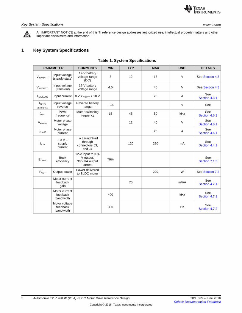
1 Key System Specifications
Table 1. System Specifications
PARAMETER COMMENTS MIN TYP MAX UNIT DETAILS
VIN(VBATT)Input voltage(steady-state)
12-V batteryvoltage range
(DC)8 12 18 V See Section 4.3
VIN(VBATT)Input voltage
(transient)12-V battery
voltage range 4.5 40 V See Section 4.3
IIN(VBATT) Input current 8 V < VBATT < 18 V 20 A SeeSection 4.3.1
IIN(12V
VBATT)REV
Input voltagereverse
Reverse batteryrange – 15 V See
fPWMPWM
frequencyMotor switching
frequency 15 45 50 kHz SeeSection 4.6.1
VPHASEMotor phase
voltage 12 40 V SeeSection 4.6.1
IPHASEMotor phase
current 20 A SeeSection 4.6.1
I3.3V
3.3 V –supplycurrent
To LaunchPadthrough
connectors J3,and J4
120 250 mA SeeSection 4.4.1
EffbuckBuck
efficiency
12-V input to 3.3-V output,
300-mA outputcurrent
70% SeeSection 7.1.5
POUT Output power Power deliveredto BLDC motor 200 W See Section 7.2
Motor currentfeedback
gain70 mV/A See
Section 4.7.1
Motor currentfeedbackbandwidth
400 kHz SeeSection 4.7.1
Motor voltagefeedbackbandwidth
300 Hz SeeSection 4.7.2
www.ti.com System Description
3TIDUBP9–June 2016Submit Documentation Feedback
Copyright © 2016, Texas Instruments Incorporated
Automotive 12 V 200 W (20 A) BLDC Motor Drive Reference Design
2 System DescriptionBrushless DC (BLDC) motors have several advantages over brushed DC (BDC) motors; these includehigher efficiency, longer lifetime and lack of brush-generated electrical noise. For these reasons, BLDCmotors are increasingly being used in automotive applications, especially for equipment that operates forlong periods of time.
TIDA-00901 is intended as a brushless DC motor drive design for automotive applications such as HVACblowers, electric pumps, cooling fans, turbo compressors, and other similar equipment. The design workswith typical 12V BLDC rotary motors where the rotational speed is regulated by controlling the PWM dutycycle. Commutation of the 3-phase brushless motor is demonstrated using sensorless technology, butboard inputs are provided in case designers wish to use Hall sensors to determine motor commutation.
All analog components critical for the motor drive design are placed in a circular footprint (2.5-inchdiameter) to replicate the typical motor drive board form factor. The board has connectors for mating to aLaunchPad™ microcontroller board, which can provide the PWM signals and communication to agraphical user interface.
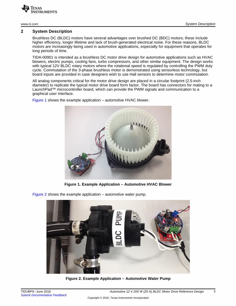
Figure 1 shows the example application – automotive HVAC blower.
Figure 1. Example Application – Automotive HVAC Blower
Figure 2 shows the example application – automotive water pump.
Figure 2. Example Application – Automotive Water Pump

Launchpad
Controller
DRV5013-Q1(optional)Position feedback
LM536003-Q1Voltage regulator
FETsFETs
FETs
LMT86-Q1Temperature
sense
C2000
Reverse battery
protection
Voltage divider
Voltage divider
DRV8305N-Q1
Motor driver
Motor feedback
Watchdog
BLDC motor up to 250 W
3.3 V
Phase voltage feedback (3)
Temperature feedback
Commutation feedback (3)
Current sense (3)Current feedback (3)
SPI
PWM (6)
12 V
USB
Block Diagram www.ti.com
4 TIDUBP9–June 2016Submit Documentation Feedback
Copyright © 2016, Texas Instruments Incorporated
Automotive 12 V 200 W (20 A) BLDC Motor Drive Reference Design
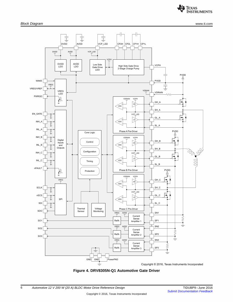
3 Block DiagramFigure 2 shows the components of a typical example application. The TIDA-00901 board includes thefunctions highlighted in the light blue rectangle. The separate LaunchPad microcontroller board includesthe C2000 real-time microcontroller and the interface to a USB connection. The brushless DC (BLDC)motor can be any appropriate three-phase model which operates on 12-V winding voltages. Hall Effectposition sensors can be used to determine motor commutation, but these sensors are not needed ifInstaSpin or an equivalent sensorless commutation algorithm is used.
Each of the board functions is described in the following sections, along with discussions regarding theselection of components making up each circuit.
Figure 3. Detailed Block Diagram

www.ti.com Block Diagram
5TIDUBP9–June 2016Submit Documentation Feedback
Copyright © 2016, Texas Instruments Incorporated
Automotive 12 V 200 W (20 A) BLDC Motor Drive Reference Design
3.1 Highlighted ProductsThis design uses the following TI products:• DRV8305-Q1 is a highly-integrated gate driver with features for automotive BLDC motor drive
applications.• LM56300-Q1 is a 650mA synchronous step-down converter with up to 2.1-MHz switching rate.• LMT86-Q1 is an analog temperature sensor with class-AB output.• DRV5013-Q1 is a Hall Effect sensor which can be used to indicate motor position for commutation.
For more information on each device and why it was chosen for this application, see the followingsections.
3.1.1 DRV8305-Q1Figure 4 shows the internal block diagram of the DRV8305N-Q1 automotive gate driver.
VREG
LDO
Digital
Inputs
and
Outputs
Core Logic
SPI
SCLK
nSCS
SDI
SDOVoltage
Monitoring
Thermal
Sensor
EN_GATE
INH_A
INL_A
nFAULT
INH_B
INL_B
INH_C
INL_C
Current
Sense
Amplifier 1
Current
Sense
Amplifier 2
Current
Sense
Amplifier 3
SN1
SP1
SN2
SP2
SN3
SP3
Ref/k
Ref/k
Ref/k
VCPH
GH_A
SH_A
GL_A
SL_A
HS
VCP_LSD
LS
VDS
VDS
VDRAIN
+
-
+
-
Phase A Pre-Driver
VCPH
GH_B
SH_B
GL_B
SL_B
HS
VCP_LSD
LS
VDS
VDS
VDRAIN
+
-
+
-
Phase B Pre-Driver
VCPH
GH_C
SH_C
GL_C
SL_C
HS
VCP_LSD
LS
VDS
VDS
VDRAIN
+
-
+
-
Phase C Pre-Driver
PVDD
PVDD
Control
Configuration
Timing
Protection PVDD
AVDD
AVDD
AVDD
VREG
VREG
VREG
High Side Gate Drive
2-Stage Charge Pump
VDRAIN
VDRAIN
PVDD
VCPH
CP1LCP1HCP2LCP2H
Low Side
Gate Drive
LDO
VCP_LSD
VCP_LSD
DVDD
LDO
AVDD
LDO
AVDDDVDD
AVDDDVDD
SO1
SO2
SO3
WAKE
VREG/VREF
PWRGD
GND PowerPADGND
VCPH
VREG
VREG
Copyright © 2016, Texas Instruments Incorporated
Block Diagram www.ti.com
6 TIDUBP9–June 2016Submit Documentation Feedback
Copyright © 2016, Texas Instruments Incorporated
Automotive 12 V 200 W (20 A) BLDC Motor Drive Reference Design
Figure 4. DRV8305N-Q1 Automotive Gate Driver

Voltage
Reference
DriverControl Logic
OSC
+
-
+
-
Control
HS Current
Sense
LS Current
Sense
COMP
Error
Amplifier
Int. Reg.
Bias
SW
BOOT
RESET
AGND
VIN
SYNC/MODE GND
EN
VCC
FB
Copyright © 2016, Texas Instruments Incorporated
www.ti.com Block Diagram
7TIDUBP9–June 2016Submit Documentation Feedback
Copyright © 2016, Texas Instruments Incorporated
Automotive 12 V 200 W (20 A) BLDC Motor Drive Reference Design
This device integrates most of the analog functions associated with controlling the drive stage for anautomotive BLDC motor into a single compact package, as shown in Figure 4.
• The three half-bridge gate drivers can source and sink 1.25 A and 1 A peak gate current, respectively.• The drive slew rate is independently programmable for the high-side and low-side FETs, with
independent control of source and sink current for optimizing the motor drive performance.• The device is rated for operation over a wide range of input voltage (4.4 V to 45 V).• Three current shunt amplifiers are integrated with programmable gain, to provide accurate motor
current feedback signals.• Monitoring and switch control of the input power is integrated to provide protection against reverse
battery faults.• The device is available qualified to AEC-Q100 temperature grade 0 or 1, which allows for operation in
automotive applications with a temperature range from –50°C to +150°C or from –40°C to +125°C,respectively.
3.1.2 LM53600N-Q1Figure 5 shows the internal block diagram of the LM53600N-Q1 synchronous step-down (buck) converter.
Figure 5. LM53600N-Q1 Synchronous Step-down (Buck) Converter
• This device has a wide operating input voltage range (3.55 V to 36 V) with transient range up to 42 V.• The device has a fixed switching frequency of 2.1 MHz, which is well above the AM radio band.• The device is available in small 3-mm × 3-mm SON package.• Spread-spectrum switching reduces peak switching noise for improved EMC performance.• The device is qualified to AEC-Q100 temperature grade 1, which allows for operation in automotive
applications with an ambient temperature range from –40°C to +125°C.
Thermal Diodes
OUT
VDD
GND
Block Diagram www.ti.com
8 TIDUBP9–June 2016Submit Documentation Feedback
Copyright © 2016, Texas Instruments Incorporated
Automotive 12 V 200 W (20 A) BLDC Motor Drive Reference Design
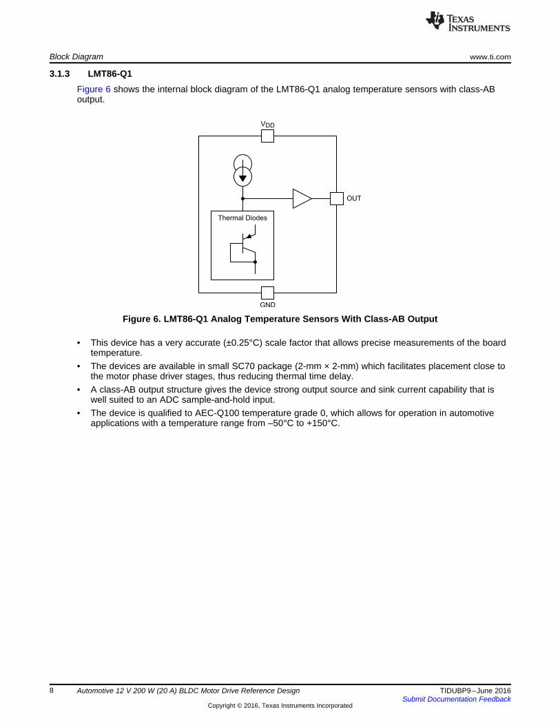
3.1.3 LMT86-Q1Figure 6 shows the internal block diagram of the LMT86-Q1 analog temperature sensors with class-ABoutput.
Figure 6. LMT86-Q1 Analog Temperature Sensors With Class-AB Output
• This device has a very accurate (±0.25°C) scale factor that allows precise measurements of the boardtemperature.
• The devices are available in small SC70 package (2-mm × 2-mm) which facilitates placement close tothe motor phase driver stages, thus reducing thermal time delay.
• A class-AB output structure gives the device strong output source and sink current capability that iswell suited to an ADC sample-and-hold input.
• The device is qualified to AEC-Q100 temperature grade 0, which allows for operation in automotiveapplications with a temperature range from –50°C to +150°C.

Temperature
CompensationBias
+
±
Offs
et C
an
ce
l
Regulated Supply
Reference
Gate
Drive
OCP
VCC
OUT
GND
2.7 to 38 V
R1
C2
(Optional)
C1
Hall Element
Copyright © 2016, Texas Instruments Incorporated
www.ti.com Block Diagram
9TIDUBP9–June 2016Submit Documentation Feedback
Copyright © 2016, Texas Instruments Incorporated
Automotive 12 V 200 W (20 A) BLDC Motor Drive Reference Design
3.1.4 DRV5013-Q1Although not part of the TIDA-00901 board, the DRV5013-Q1 is an example of an appropriate Hall Effectdevice for use in applications where sensorless commutation is used. For these applications, theDRV5013-Q1 would typically be mounted on the motor assembly, to provide position feedback.
Figure 7 shows the internal block diagram of the DRV5013-Q1 automotive digital-latch hall effect sensor.
Figure 7. DRV5013-Q1 Automotive Digital-Latch Hall Effect Sensor
• This device supports a wide Voltage range (2.7 to 38 V) making it adaptable to a broad range ofmotors and interface options.
• This device has excellent temperature stability (BOP ±10% over temperature) which is important formotor-mounted applications where the device will be subjected to wide temperature variations.
• The device is available in a small package for space-constrained applications.• The device has several integrated protection features, which are important because it will be
connected remotely from the bias voltage and signals may be subjected to wiring faults.– Protection features reverse supply protection (up to –22 V)– Supports up to 40-V load dump– Output short-circuit protection– Output current limitation– OUT short to battery protection
• The device is available qualified to AEC-Q100 temperature grade 0 or 1, which allows for operation in

Laun
chpa
d
Con
nect
ors
Gate driver with currentsense and diagnostics
3.3-V buck
12-V input,reverse-battery
protection and filtering
3-phase motor drive stages
System Design Theory www.ti.com
10 TIDUBP9–June 2016Submit Documentation Feedback
Copyright © 2016, Texas Instruments Incorporated
Automotive 12 V 200 W (20 A) BLDC Motor Drive Reference Design
automotive applications with a temperature range from –50°C to +150°C or from –40°C to +125°C,respectively.
4 System Design TheoryThe following sections describe the considerations behind the design of each part of the system.
4.1 PCB and Form FactorThe goals for the board geometry were:• Compatible with LaunchPad microcontroller development platform• Circular board shape to demonstrate typical form factor for rotary motors• Easy access to significant electrical test points on LaunchPad connectors• Single side component mounting for ease of assembly and debug
The layout concept locates the circuitry actively driving the motor within a circular area in the center of theboard. Connectors are along the outside of the circular board and were selected for ease of use, ratherthan suitability for a production design. The LaunchPad microcontroller board is mounted on connectorswithin the circle, and this arrangement allows designers to use a variety of specific microcontrollers,depending on the requirements of the application.
Figure 8 shows the TIDA-00901 board simplified board floor plan.
Figure 8. TIDA-00901 Board Simplified Floor Plan
4.2 Overall Considerations for Component SelectionIn general, components were selected based on the performance requirements of the expectedapplications. Where practical, components with automotive ratings were selected. For active components,the components selected are AEC-Q100 qualified to either temperature grade 0 or temperature grade 1.
Capacitors are generally X7R grade (−55°C to +125°C) or higher, with size and value selected for theexpected extremes of operation conditions. The voltage rating of the capacitors must be greater than themaximum voltage they could experience, and 2x the typical operating voltage to avoid DC bias effects.The amount of output capacitance used depends on output ripple and transient response requirements,and many equations and tools are available online to help estimate these values.

www.ti.com System Design Theory
11TIDUBP9–June 2016Submit Documentation Feedback
Copyright © 2016, Texas Instruments Incorporated
Automotive 12 V 200 W (20 A) BLDC Motor Drive Reference Design
Consider the possible maximum voltage that could be experienced by the components. Capacitors mustbe derated by a minimum of 25% due to the drop in capacitance at 100% rated DC voltage of X7R andC0G/NP0 ceramic capacitors (that is, Max voltage 40 V; Capacitor voltage rating = 40V * 1.25 = 50V). Thederating also helps protect components from unexpected voltage spikes in the system. During the designprocess the amount of BOM line items was considered. Therefore, capacitor voltage ratings may havebeen increased above the minimum desired rating. As an example, if there was one 1-μF, 25-V capacitorbut nine 1-μF, 50-V capacitors, then the lone 25-V capacitor was modified to become a 50-V capacitorand the schematic contains a note indicating that the voltage rating was increased for BOM simplicity.
Supplies in this solution were designed for a ±2.5% (5%) total transient response. Low-ESR ceramiccapacitors were used exclusively to reduce ripple. For internally compensated supplies, see device-specific data sheets, because they may have limitations on acceptable LC output filter values.
For improved accuracy, all feedback resistor dividers must use components with 1% or better tolerance.Resistance tolerance in this design was selected to reduce the total amount of BOM line items. In thedesign considerations, it is noted where 5% or 10% precision resistors may be used to reduce the cost ofa specific individual resistor. Using less precise resistors for cost reasons should be weighed againstreducing the amount of BOM line items and ordering in higher volumes to reduce total BOM cost.
Zero-Ohm (0-Ω) resistors are used at the input and output of some of the circuit sections for testingpurposes only, and could be removed, if required, in a production board design.
4.3 12-V Input ProtectionReverse Battery ProtectionThe 12-V supply may experience several excursions from the nominal 12-V value. This design includesprotection against such typical hazards as reverse battery conditions, and high-frequency electrical noise.
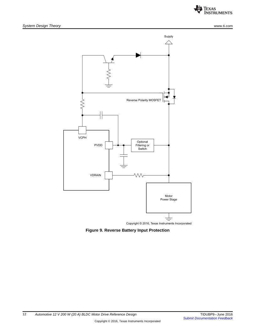
Reverse battery protection is required in nearly every electronic subsystem of a vehicle, both by OEMstandards, as well as ISO 16750-2, an international standard pertaining to supply quality. The DRV8305 isdesigned to support an external reverse supply protection scheme. The VCPH high-side charge pump isable to supply an external load up to 10 mA. This feature allows implementation of an external reversebattery protection scheme using a MOSFET and a BJT, as shown in Figure 9.
The MOSFET gate and BJT may be driven by VCPH with a current limiting resistor. The current limitingresistor must be sized not to exceed the maximum external load on VCPH; R1 has a value of 10 kΩ,limiting the load on VCPH to less than 1 mA.
For this design, the Reverse Polarity MOSFET (see Section 8) must be rated at least as high as theexpected input voltage; the SQJ422EP is rated for 40 V. Compared to the FETs used to drive the motorphases, there is no emphasis on switching speed for the reverse-polarity FET, therefore, this device wasselected primarily based on a low on-state resistance, rather than low gate capacitance (see Table 3).
The VDRAIN sense pin is protected against reverse supply conditions by use of a current limiting resistor,R20. The current limit resistor must be sized not to exceed the maximum current load on the VDRAIN pin.As recommended, (see DRV8305-Q1 Three-Phase Automotive Smart Gate Driver With Three IntegratedCurrent Shunt Amplifiers and Voltage Regulatordatasheet (SLVSD12) R20 has a value of 100 Ω betweenVDRAIN and the drain of the external high-side MOSFET.
The BJT (Q1) and diode (D1) serve to pull the gate of the FET low when reverse battery conditions exist.This prevents any inadvertent turn-on of the reverse polarity FET due to sneak paths.
VDRAIN
PVDD
VCPH
Optional
Filtering or
Switch
Motor
Power Stage
Reverse Polarity MOSFET
Supply
Copyright © 2016, Texas Instruments Incorporated
System Design Theory www.ti.com
12 TIDUBP9–June 2016Submit Documentation Feedback
Copyright © 2016, Texas Instruments Incorporated
Automotive 12 V 200 W (20 A) BLDC Motor Drive Reference Design
Figure 9. Reverse Battery Input Protection
( ) ( )2 2
L1 L1P I R 20 0.00255 1.02 W= ´ = ´ =
www.ti.com System Design Theory
13TIDUBP9–June 2016Submit Documentation Feedback
Copyright © 2016, Texas Instruments Incorporated
Automotive 12 V 200 W (20 A) BLDC Motor Drive Reference Design
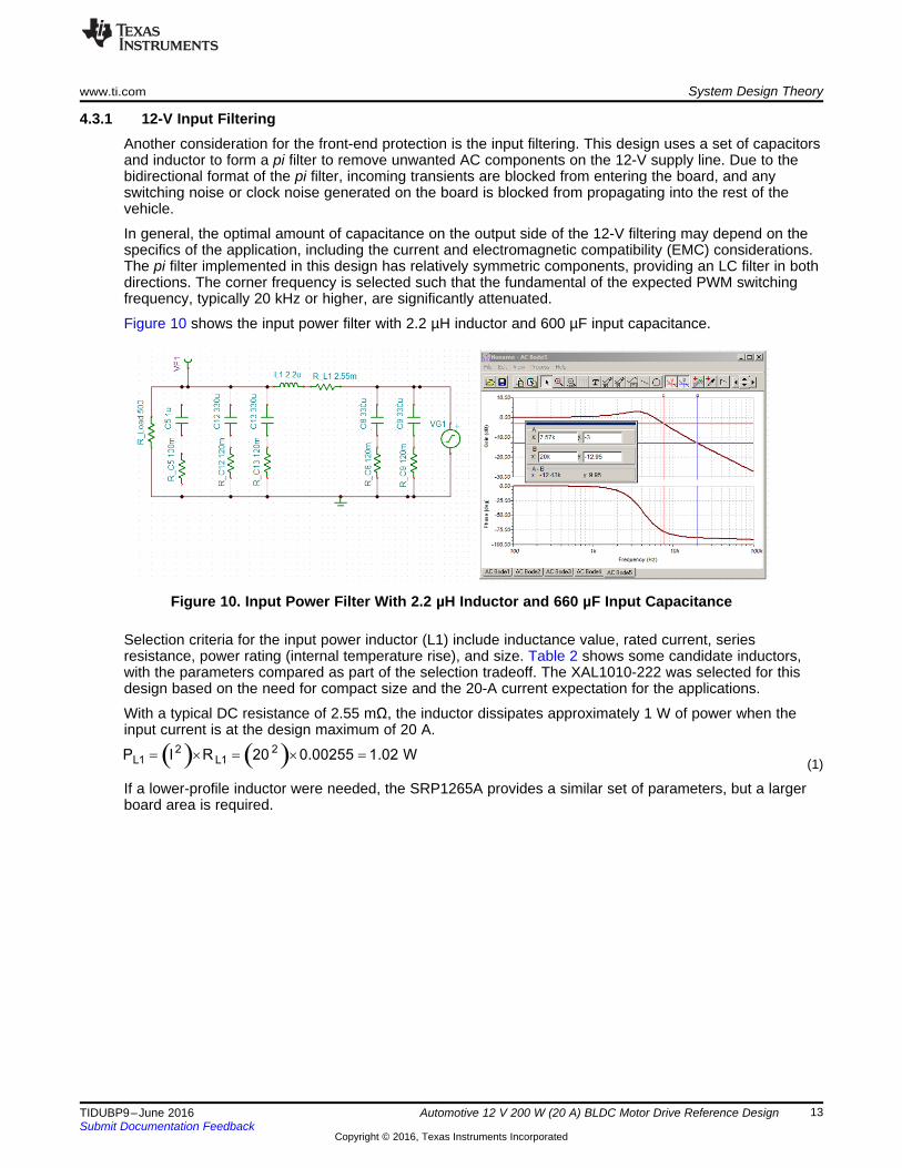
4.3.1 12-V Input FilteringAnother consideration for the front-end protection is the input filtering. This design uses a set of capacitorsand inductor to form a pi filter to remove unwanted AC components on the 12-V supply line. Due to thebidirectional format of the pi filter, incoming transients are blocked from entering the board, and anyswitching noise or clock noise generated on the board is blocked from propagating into the rest of thevehicle.
In general, the optimal amount of capacitance on the output side of the 12-V filtering may depend on thespecifics of the application, including the current and electromagnetic compatibility (EMC) considerations.The pi filter implemented in this design has relatively symmetric components, providing an LC filter in bothdirections. The corner frequency is selected such that the fundamental of the expected PWM switchingfrequency, typically 20 kHz or higher, are significantly attenuated.
Figure 10 shows the input power filter with 2.2 µH inductor and 600 µF input capacitance.
Figure 10. Input Power Filter With 2.2 µH Inductor and 660 µF Input Capacitance
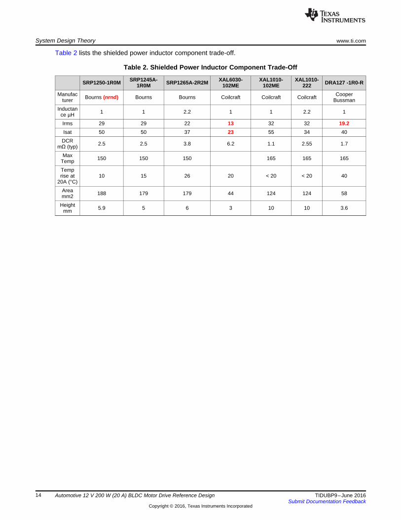
Selection criteria for the input power inductor (L1) include inductance value, rated current, seriesresistance, power rating (internal temperature rise), and size. Table 2 shows some candidate inductors,with the parameters compared as part of the selection tradeoff. The XAL1010-222 was selected for thisdesign based on the need for compact size and the 20-A current expectation for the applications.
With a typical DC resistance of 2.55 mΩ, the inductor dissipates approximately 1 W of power when theinput current is at the design maximum of 20 A.
(1)
If a lower-profile inductor were needed, the SRP1265A provides a similar set of parameters, but a largerboard area is required.
System Design Theory www.ti.com
14 TIDUBP9–June 2016Submit Documentation Feedback
Copyright © 2016, Texas Instruments Incorporated
Automotive 12 V 200 W (20 A) BLDC Motor Drive Reference Design
Table 2 lists the shielded power inductor component trade-off.
Table 2. Shielded Power Inductor Component Trade-Off
SRP1250-1R0M SRP1245A-1R0M SRP1265A-2R2M XAL6030-
102MEXAL1010-
102MEXAL1010-
222 DRA127 -1R0-R
Manufacturer Bourns (nrnd) Bourns Bourns Coilcraft Coilcraft Coilcraft Cooper
BussmanInductan
ce µH 1 1 2.2 1 1 2.2 1
Irms 29 29 22 13 32 32 19.2Isat 50 50 37 23 55 34 40
DCRmΩ (typ) 2.5 2.5 3.8 6.2 1.1 2.55 1.7
MaxTemp 150 150 150 165 165 165
Temprise at
20A (°C)10 15 26 20 < 20 < 20 40
Areamm2 188 179 179 44 124 124 58
Heightmm 5.9 5 6 3 10 10 3.6

Reverse battery and filter
Buck
VBATT PVDD
3.3 V
www.ti.com System Design Theory
15TIDUBP9–June 2016Submit Documentation Feedback
Copyright © 2016, Texas Instruments Incorporated
Automotive 12 V 200 W (20 A) BLDC Motor Drive Reference Design
4.4 Power SuppliesThe motor drive stage switches power from the filtered 12-V supply. A 3.3-V supply provides power to theLaunchPad microcontroller circuits, as well as the on-board temperature sensor and the optional HallEffect sensors. Figure 11 shows the power supply scheme.
Figure 11. Power Supply Scheme
4.4.1 3.3-V Step-Down (Buck) RegulatorThe design is intended to operate from a standard 12-V automotive battery. The battery voltage may varyover a range of input voltages from 4.5 V to 40 V. However, input voltages below 8 V (due to enginecrank) or above 18 V (due to load dump) are expected to be short transient conditions.
The 3.3-V power supplies the C2000 real-time microcontroller LaunchPad board, the temperature sensorand reference voltage on the BoosterPack board, and the optional off-board Hall Effect sensors. Totalcurrent from the 3.3-V supply is not expected to exceed 250 mA.
To reduce component size and eliminate switching noise in the AM radio band, a synchronous buckregulator with high switching frequency is desirable. The LM536003-Q1 has a switching frequency of 2.1MHz and provides synchronous regulation for currents up to 650 mA. The small (3 mm × 3 mm) packageand few external components meet the desire for a compact design.
The N version of the LM53600 implements spread spectrum eliminates peak emissions at specificfrequencies by spreading emissions across a wider range of frequencies than a part with fixed frequencyoperation. Typically, low frequency conducted emissions from the first few harmonics of the switchingfrequency are easily filtered. A more difficult design criterion is reduction of emissions at higher harmonicswhich fall in the FM band. These harmonics often couple to the environment through electric fields aroundthe switch node. The LM53600-Q1 and LM53601-Q1 devices use a ±4% spread of frequencies whichspread energy smoothly across the FM band but is small enough to limit sub-harmonic emissions belowits switching frequency. Peak emissions at the part’s switching frequency are only reduced by slightly lessthan 1 dB, while peaks in the FM band are typically reduced by more than 6 dB.
The LM53600-Q1 device uses a cycle to cycle frequency hopping method based on a linear feedback shiftregister (LFSR). Intelligent pseudo random generator limits cycle to cycle frequency changes to limitoutput ripple. Pseudo random pattern repeats by approximately 7 Hz, which is below the audio band.
Due to the fixed output voltage and internal compensation of the LM53600N-Q1, few external componentsare required. The choice of inductor is important, and a key feature for this design are compact footprintand sufficient current rating. The saturation current of L2 is 1.5 A, which is higher than threshold forLM53600N-Q1 hiccup feature, ensuring no issues in the event of a short-circuit fault on the 3.3-V supplyoutput. The short-circuit falt tolerance is an important benefit because the 3.3-V supply is available onconnector pins to supply the LaunchPad board.
Figure 12 shows the 12-V to 3.3-V buck regulator schematic.

3.3V
22µFC35
Orange
12
D3
PVDD
1µFC34
GND
10µFC33
0.1µFC37
0.01µFC38
330R31
600 ohm
L3
0.1µF
C32
4.7µH
L2
0.1µFC14
SW1
BOOT2
VCC3
FB4
AGND5
RESET6
EN7
VIN8
SYNC/MODE9
GND10
PAD11
U4
LM53600NQDSXRQ1
Copyright © 2016, Texas Instruments Incorporated
System Design Theory www.ti.com
16 TIDUBP9–June 2016Submit Documentation Feedback
Copyright © 2016, Texas Instruments Incorporated
Automotive 12 V 200 W (20 A) BLDC Motor Drive Reference Design
Figure 12. 12-V to 3.3-V Buck Regulator Schematic
TI's on-line design tool, Webench® was used to select the components for the 3.3-V buck regulator.Webench also provides a means to simulate the performance of the design; some of the simulation resultsare shown in the following figures.
Figure 13 shows the frequency response of the 3.3-V buck regulator control loop. The zero dB crossoverfrequency is about 60 kHz, which is sufficient to regulate and reject any anticipated disturbances. The loopsimulation shows a phase margin of approximately 50 degrees, and a gain margin of over 20 dB,indicating the loop compensation has resulted in a very stable configuration.
Figure 13. Bode Plot Simulation of the 3.3-V Buck Regulator Design
The response to an abrupt change in the input voltage is simulated as shown in Figure 14. Here, the input(PVDD) transitions from 5 V to 18 V and then back to 5 V. The response of the regulator is a smallexcursion in the output voltage, which quickly returns to the regulated value.

www.ti.com System Design Theory
17TIDUBP9–June 2016Submit Documentation Feedback
Copyright © 2016, Texas Instruments Incorporated
Automotive 12 V 200 W (20 A) BLDC Motor Drive Reference Design
The abrupt changes shown in Figure 14 are intended to illustrate worst-case conditions; in real operation,even a cold-crank or stop and start event would not be expected to have this extreme of a voltage change.
Figure 14. Simulation of Large Transient on Input to 3.3-V Buck Regulator Design
4.5 Gate DriverThe motor drive stage delivers 12-V power to the three phases of the BLDC motor as a pulse-widthmodulated (PWM) voltage. An overview of the gate driver circuit and motor stages is shown in Figure 15.
Each high-side and low-side pre-driver receives PWM signals from the microcontroller and generates thecorresponding level-shifted (higher amplitude) signals to drive the gates of the high-side MOSFET andlow-side MOSFET . The DRV8305N-Q1 gate driver is biased by the PVDD supply, with allowable supplytolerance from 4.4 V to 45 V.
The PWM switching frequency may range up to 200 kHz. This frequency is set by the parameters of theMotorWare software running on the LaunchPad microcontroller board. Unless otherwise noted, the PWMswitching frequency was set to 45 kHz in the tests that follow.
Compared to other drive stage designs, there are very few external components around the drive FETs inthis reference design. This reduction in external components is possible because the DRV8305-Q1 hasseveral features that allow programming the parameters associated with the drive stage, to optimize themotor drive performance and reduce electromagnetic compatibility (EMC) concerns.

Core Logic
Voltage
Monitoring
Thermal
Sensor
VCPH
GH_A
SH_A
GL_A
SL_A
HS
VCP_LSD
LS
VDS
VDS
VDRAIN
+
-
+
-
Phase A Pre-Driver
VCPH
GH_B
SH_B
GL_B
SL_B
HS
VCP_LSD
LS
VDS
VDS
VDRAIN
+
-
+
-
Phase B Pre-Driver
VCPH
GH_C
SH_C
GL_C
SL_C
HS
VCP_LSD
LS
VDS
VDS
VDRAIN
+
-
+
-
Phase C Pre-Driver
PVDD
Control
Configuration
Timing
Protection PVDD
Copyright © 2016, Texas Instruments Incorporated
System Design Theory www.ti.com
18 TIDUBP9–June 2016Submit Documentation Feedback
Copyright © 2016, Texas Instruments Incorporated
Automotive 12 V 200 W (20 A) BLDC Motor Drive Reference Design
Figure 15. Motor Drive Circuit Overview
In addition to supplying gate drive current to the drive stage FETs, the DRV8305-Q1 has several otherfunctions. These functions include three current sense amplifiers (CSA) used to amplify the signal whichmeasures the current through each phase of the motor. The DRV8305-Q1 also controls the external circuitwhich disconnects the circuits on this board from the input power voltage in the case of a reverse polaritycondition. These functions are discussed separately in the following sections.
4.6 Motor Drive StagesThe motor drive stage consists of the three pairs of n-channel MOSFETs (high-side and low-side), one foreach of the three phases of the BLDC motor, and the large capacitors which supply the immediate burstsof current during each FET transition. Due to the integrated features of the DRV8305-Q1 gate driver, fewother components are needed to optimize the performance of the drive stage.

( )( )GD MAX
sw MAXFETs G G
I 30 mAf
N Q 6 Q= =
´ ´
www.ti.com System Design Theory
19TIDUBP9–June 2016Submit Documentation Feedback
Copyright © 2016, Texas Instruments Incorporated
Automotive 12 V 200 W (20 A) BLDC Motor Drive Reference Design
4.6.1 FET SelectionSelection of the field-effect transistors (FETs) for the motor drive stages involves a trade-off betweencomponent size, on-state resistance, and gate capacitance or charge.
Table 3 lists some of the candidate FETs considered for the drive stages. All of the drive stages meet therequirements for high voltage specifications on the drain-to-source (at least 40 V), and a small size (32mm2 board area). All drive stages are rated for at least 20 A of current, and have low RDS(ON) forreducing conductive losses (<10 m
Table 3. Power FET Component Trade-Off
CSD18540Q5B AUIRF7648M2 AUIRFN7107 SQJ858AEP SQJ460AEP SQJ422EP
Manufacturer TI Infenion Infineon Vishay Vishay VishayVDS (max) 60 60 75 40 60 40Automotive No Yes Yes Yes Yes YesMax Temp 150 175 175 175 175 175
Max Current 221 68 75 58 27 at 125 C 62 at 125 CRDS (on) max
(mΩ) 2.2 at 25 C 7 8.5 6.3 at 25 C 8.7 at 25 C 3.4 at 25 C
Total GateChange
(Max) (nC)53 53 77 55 106 100
QGD typ (nC) 6.7 14 14 6 12.5 10.3
Package SON 5 × 6 Direct FET 6.3 ×5 PQFN 5 × 6 SO-8L
5.13 × 6.15SO-8L
5.13 × 6.15SO-8L
5.13 × 6.15Area 30 32 30 32 32 32
For this design, a PWM switching frequency of up to 50 kHz is specified; the DRV8305-Q1 allowsswitching rates up to 200 kHz. However, another design consideration is that the DRV8305-Q1 is rated fora maximum average gate drive current of 30 mA. This maximum gate drive current of 30 mA sets anupper limit on the product of the PWM switching frequency multiplied by the total gate charge of the driveFETs.
As discussed in the section Gate Drive Average Current of the DRV8305-Q1 Three-Phase AutomotiveSmart Gate Driver With Three Integrated Current Shunt Amplifiers and Voltage Regulator datasheet(SLVSD12A), the maximum switching frequency is a function of the gate charge of the FETs selected forthe drive stages.
(2)
PW
M S
witc
hing
Fre
quen
cy (
kHz)
0
10
20
30
40
50
60
70
80
90
100
CSD18540Q5B AUIRF7648M2 AUIRFN7107 SQJ858AEP SQJ460AEP SQJ422EP
D001
System Design Theory www.ti.com
20 TIDUBP9–June 2016Submit Documentation Feedback
Copyright © 2016, Texas Instruments Incorporated
Automotive 12 V 200 W (20 A) BLDC Motor Drive Reference Design
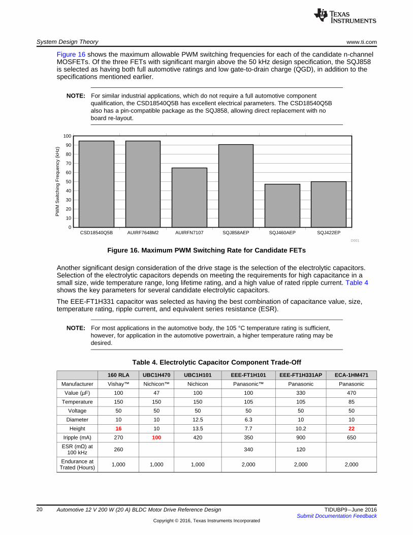
Figure 16 shows the maximum allowable PWM switching frequencies for each of the candidate n-channelMOSFETs. Of the three FETs with significant margin above the 50 kHz design specification, the SQJ858is selected as having both full automotive ratings and low gate-to-drain charge (QGD), in addition to thespecifications mentioned earlier.
NOTE: For similar industrial applications, which do not require a full automotive componentqualification, the CSD18540Q5B has excellent electrical parameters. The CSD18540Q5Balso has a pin-compatible package as the SQJ858, allowing direct replacement with noboard re-layout.
Figure 16. Maximum PWM Switching Rate for Candidate FETs
Another significant design consideration of the drive stage is the selection of the electrolytic capacitors.Selection of the electrolytic capacitors depends on meeting the requirements for high capacitance in asmall size, wide temperature range, long lifetime rating, and a high value of rated ripple current. Table 4shows the key parameters for several candidate electrolytic capacitors.
The EEE-FT1H331 capacitor was selected as having the best combination of capacitance value, size,temperature rating, ripple current, and equivalent series resistance (ESR).
NOTE: For most applications in the automotive body, the 105 °C temperature rating is sufficient,however, for application in the automotive powertrain, a higher temperature rating may bedesired.
Table 4. Electrolytic Capacitor Component Trade-Off
160 RLA UBC1H470 UBC1H101 EEE-FT1H101 EEE-FT1H331AP ECA-1HM471Manufacturer Vishay™ Nichicon™ Nichicon Panasonic™ Panasonic Panasonic
Value (µF) 100 47 100 100 330 470Temperature 150 150 150 105 105 85
Voltage 50 50 50 50 50 50Diameter 10 10 12.5 6.3 10 10
Height 16 10 13.5 7.7 10.2 22Iripple (mA) 270 100 420 350 900 650ESR (mΩ) at
100 kHz 260 340 120
Endurance atTrated (Hours) 1,000 1,000 1,000 2,000 2,000 2,000

2T
IN2
a Ta
V 1I 1 e
R
1 e
-t
-t
æ öæ öç ÷ç ÷D = -ç ÷ç ÷ç ÷è ø-è ø
2 1
a a aI I ID = -
DT
a IN2
a Ta a
E V 1 eI
R R
1 e
-
t
-
t
-= - + ´
-
( )1 D T T
a IN1
a Ta a
E V e eI
R R
1 e
--
t t
-t
-= - + ´
-
( ) ( )2 1
ac a ao aI DT I and I T I= =
( ) ( ) ( )( )a at DT / t DT /2
ao a
a a
E LI t I e 1 e in which
R R
- - t - - t= - - t =
( ) ( )IN a a1 t/ t/
ac a
a a
V E LI t I e 1 e in which
R R
- t - t-
= + - t =
T 2T t
I ARM
2aI
1aI
www.ti.com System Design Theory
21TIDUBP9–June 2016Submit Documentation Feedback
Copyright © 2016, Texas Instruments Incorporated
Automotive 12 V 200 W (20 A) BLDC Motor Drive Reference Design
Ripple current is the AC current flowing in the capacitor due to motor switching currents. The ripple currentheats the capacitor, and the maximum permitted ripple current is set by how much is permitted while stillmeeting the capacitor’s load life specification. Too much temperature rise causes the capacitor to exceedits maximum permitted core temperature and fail quickly, however, operation close to the maximumpermitted core temperature dramatically shortens expected life. The load life specifications for aluminumelectrolytic capacitors operating at maximum permitted core temperature are typically 1,000 to 10,000hours.
To keep the ripple current low, the PWM frequency should be such that the PWM period (T) is significantlyshorter than the electrical time constant of the motor winding (τ = L/R).
Figure 17 shows how the motor current varies during PWM switching.
Figure 17. Motor Current Varies During PWM Switching
In a motor, the current is found for both when the controllable switch (MOSFET) is open and closed. If theswitch closed current is called Iac then,
(3)
If the motor current when the switch, S1, is open is called Iao, then
(4)
The quantities of Ia2 and Ia1 may be found by recognizing that
(5)
Solve the above two equations simultaneously to obtain
(6)
and
(7)
The amount of ripple current is given by
(8)
The ripple current is maximized when the duty-cycle D = 0.5 (and is zero when D = 0 or D = 1). For this50% duty cycle condition, the worst case is when the motor is stationary (start-up or stall condition) andthus the back EMF is zero. Then the maximum ripple current is
(9)

Ratio of T to W
Rip
ple
Cur
rent
as
a F
ract
ion
of V
/ R
a
0 0.2 0.4 0.6 0.8 1 1.20
0.05
0.1
0.15
0.2
0.25
0.3
D002
System Design Theory www.ti.com
22 TIDUBP9–June 2016Submit Documentation Feedback
Copyright © 2016, Texas Instruments Incorporated
Automotive 12 V 200 W (20 A) BLDC Motor Drive Reference Design
For relatively short PWM periods (less than the electrical time constant of the motor), this relationship isfairly linear, as shown in Figure 18. The motor electrical time constant is typically on the order of 1millisecond, so a typical PWM frequency of 40 kHz gives a T to τ ratio of 1 ÷ 40, or 0.025. The ripplecurrent then is on the order of 0.6% of the motor stall current. The capacitors selected for this design havea rated ripple current of 900 mA; to keep the actual ripple current well below this value, a motor with stallcurrent on the order of 80 A is driven with a PWM frequency of 40 kHz or more. This combination offrequency and motor stall current limits the maximum ripple current to about 500 mA.
Figure 18. Normalized Plot of Ripple Current vs PWM Period
www.ti.com System Design Theory
23TIDUBP9–June 2016Submit Documentation Feedback
Copyright © 2016, Texas Instruments Incorporated
Automotive 12 V 200 W (20 A) BLDC Motor Drive Reference Design
4.7 Motor Control FeedbackThe algorithm for controlling the motor makes use of sampled measurements of the motor conditions,including 12-V supply voltage, the voltage on each motor phase, the current of each motor phase, and inthe case of sensored communication, the position feedback from motor-mounted sensors such as HallEffect sensors. For reliability, the temperature of the motor drive stage is also monitored.
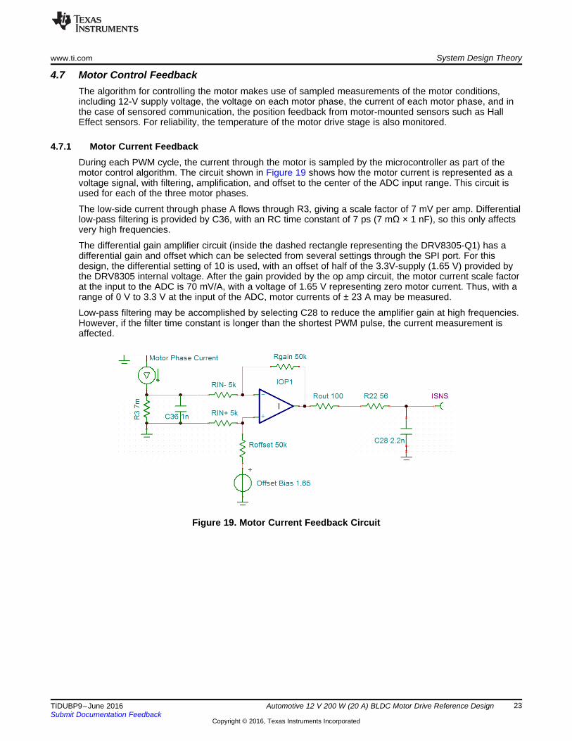
4.7.1 Motor Current FeedbackDuring each PWM cycle, the current through the motor is sampled by the microcontroller as part of themotor control algorithm. The circuit shown in Figure 19 shows how the motor current is represented as avoltage signal, with filtering, amplification, and offset to the center of the ADC input range. This circuit isused for each of the three motor phases.
The low-side current through phase A flows through R3, giving a scale factor of 7 mV per amp. Differentiallow-pass filtering is provided by C36, with an RC time constant of 7 ps (7 mΩ × 1 nF), so this only affectsvery high frequencies.
The differential gain amplifier circuit (inside the dashed rectangle representing the DRV8305-Q1) has adifferential gain and offset which can be selected from several settings through the SPI port. For thisdesign, the differential setting of 10 is used, with an offset of half of the 3.3V-supply (1.65 V) provided bythe DRV8305 internal voltage. After the gain provided by the op amp circuit, the motor current scale factorat the input to the ADC is 70 mV/A, with a voltage of 1.65 V representing zero motor current. Thus, with arange of 0 V to 3.3 V at the input of the ADC, motor currents of ± 23 A may be measured.
Low-pass filtering may be accomplished by selecting C28 to reduce the amplifier gain at high frequencies.However, if the filter time constant is longer than the shortest PWM pulse, the current measurement isaffected.
Figure 19. Motor Current Feedback Circuit

System Design Theory www.ti.com
24 TIDUBP9–June 2016Submit Documentation Feedback
Copyright © 2016, Texas Instruments Incorporated
Automotive 12 V 200 W (20 A) BLDC Motor Drive Reference Design
Figure 20 shows the frequency response of the motor current sense amplifier circuit as simulated in theTina-TI circuit simulation tool. As expected, the low frequency gain is -23 dB, and the corner frequency isabout 450 kHz for these values of R22 and C28.
Figure 20. Simulated Frequency Response of the Current Sense Amplifier Circuit
4.7.2 Motor Voltage FeedbackThe voltage of each of the three motor phases is sampled by the microcontroller as part of the motorcontrol algorithm. The circuit shown in Figure 21 shows how the motor voltage is filtered and scaled forthe ADC input range. A fourth identical circuit is used to measure the 12-V supply applied to all three ofthe motor phase drive circuits.
Figure 21. Motor Voltage Feedback Circuit
www.ti.com System Design Theory
25TIDUBP9–June 2016Submit Documentation Feedback
Copyright © 2016, Texas Instruments Incorporated
Automotive 12 V 200 W (20 A) BLDC Motor Drive Reference Design
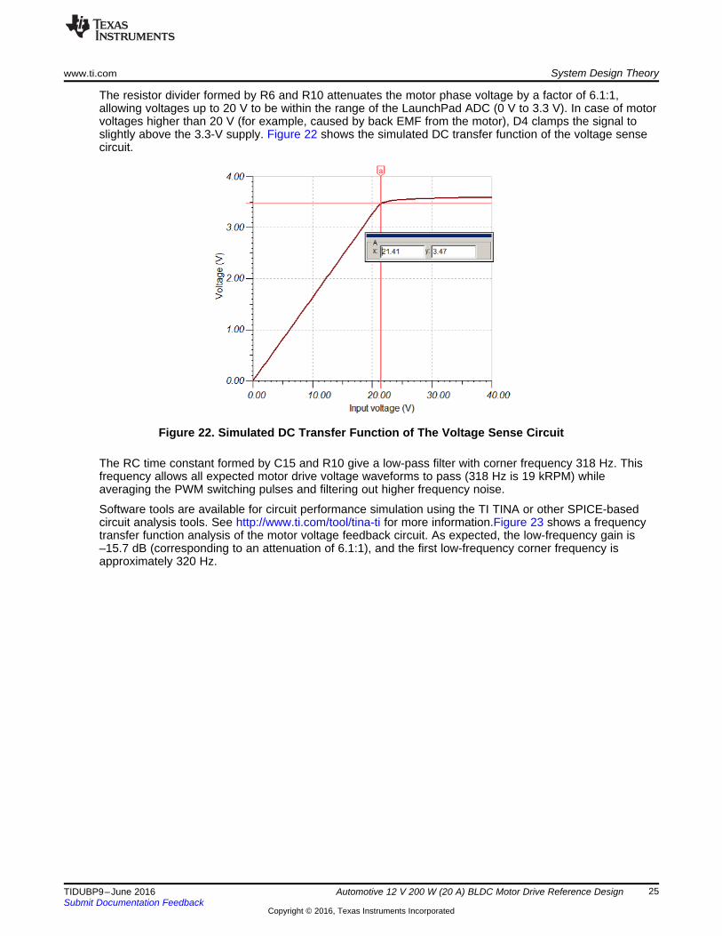
The resistor divider formed by R6 and R10 attenuates the motor phase voltage by a factor of 6.1:1,allowing voltages up to 20 V to be within the range of the LaunchPad ADC (0 V to 3.3 V). In case of motorvoltages higher than 20 V (for example, caused by back EMF from the motor), D4 clamps the signal toslightly above the 3.3-V supply. Figure 22 shows the simulated DC transfer function of the voltage sensecircuit.
Figure 22. Simulated DC Transfer Function of The Voltage Sense Circuit
The RC time constant formed by C15 and R10 give a low-pass filter with corner frequency 318 Hz. Thisfrequency allows all expected motor drive voltage waveforms to pass (318 Hz is 19 kRPM) whileaveraging the PWM switching pulses and filtering out higher frequency noise.
Software tools are available for circuit performance simulation using the TI TINA or other SPICE-basedcircuit analysis tools. See http://www.ti.com/tool/tina-ti for more information.Figure 23 shows a frequencytransfer function analysis of the motor voltage feedback circuit. As expected, the low-frequency gain is–15.7 dB (corresponding to an attenuation of 6.1:1), and the first low-frequency corner frequency isapproximately 320 Hz.

( )diode
40 V 3.3 V 0.4 Vi 1.4 mA
25.5 k
- += =
W
System Design Theory www.ti.com
26 TIDUBP9–June 2016Submit Documentation Feedback
Copyright © 2016, Texas Instruments Incorporated
Automotive 12 V 200 W (20 A) BLDC Motor Drive Reference Design
Figure 23. Simulated Frequency Transfer Results for Voltage Feedback Circuit
Selection of the clamping diodes is based on size, forward voltage drop, breakdown voltage and pad pitch.The BAT54CDW was selected as having the best combination of low forward voltage, high reversebreakdown voltage, and pad pitch easily assembled by most board shops.
Table 5 shows the clamping diode selection criteria.
Table 5. Clamping Diode Selection Criteria
RB521ZS8A30TE61 QSG0115UDJ-7 BAT54CDW NUP4201 1N4448Manufacturer Rohm™ Diodes™ Diodes ON Semi™ Diodes
Type Schottky Schottky Schottky TVS Fast SwitchingDiodes 4 4 4 9 1
Vf at 10 mA(maximum) 370 mV 400 mV 400 mV Not Specified 0.855
Capacitance(pF) 7 maximum 3 typical, 8
maximum 10 maximum 3 typical maximum 4 maximum
Size 1.60 × 0.80 1.05 × 1.05 2.1 × 2.0 3.00 × 2.75 1.55 × 3.7Pad Pitch(min) mm 0.4 0.35 0.65 1.27 2.25
BreakdownVoltage > 30 V > 15 V > 30 V > 6 V 75
MaximumTemperature 150 C 150 C 125 C 125 C 150
If the maximum expected voltage on the motor signals is 40V, the current through the clamping diodes willbe less than 2 mA:
(10)
Therefore, power dissipation in the clamping diodes is not a concern for this level of signal.

1000pF
C25
1000pF
C26
1000pF
C27
HALL_A
GND
HALL_BHALL_C
POSN_A
POSN_B
POSN_C
3.3V
1
2
3
4
5
J5
PPTC051LFBN-RC
1.0kR16
1.0kR17
1.0kR18
10k
R19
10k
R21
10k
R24
15kR26
15kR27
15kR28
0R15
Copyright © 2016, Texas Instruments Incorporated
www.ti.com System Design Theory
27TIDUBP9–June 2016Submit Documentation Feedback
Copyright © 2016, Texas Instruments Incorporated
Automotive 12 V 200 W (20 A) BLDC Motor Drive Reference Design
4.7.3 Motor Drive Temperature FeedbackThe temperature of the motor drive MOSFETs is sampled by the microcontroller as part of the motordiagnostic scheme. Figure 24 shows the motor drive temperature scale.
Figure 24. Motor Drive Temperature Scale
The scale factor from the LMT86 is –10.9 mV/°C with a range of –50°C to +150°C, covering an outputrange of 0.4 V to 2.6 V, which is within the input voltage range of the ADC. Due to the integrated featuresof the LMT86-Q1, very few external components are required.
4.7.4 Motor Position Feedback (Hall Effect Sensors)Some applications may make use of Hall Effect sensors such as the DRV5013-Q1 or similar sensors toprovide motor position feedback to the motor controller, facilitating simplified commutation of the 3-phasebrushless motor. This design includes components to bias and buffer those signals, as shown inFigure 25.
Figure 25. Connections to Optional External Hall Effect Sensors
The 1-kΩ resistors (R16-R18) provide pull-up to allow connection to sensors with open-collector outputs.With R15 installed, the pull-up voltage is the 3.3-V supply generated on the board. If a different pull-upvoltage is needed, R15 may be removed, and the alternate voltage supplied on pin J5-5.
In all cases, the resistor values R19, R21, R24 and R26-R28 can be changed to provide any signalattenuation needed to adjust incoming Hall Effect signals with higher voltage levels to match the 3.3-Vsignal levels expected at the interface to the LaunchPad microcontroller board.
1
3
56
4
2
7
910
8
12 11
14 13
16 15
18 17
20 19
J31
3
56
4
2
7
910
8
12 11
14 13
16 15
18 17
20 19
J4
nFAULT
SCLK
VSEN_AVSEN_BVSEN_CVSEN_PVDD
GND
PWM_AHPWM_ALPWM_BHPWM_BLPWM_CHPWM_CL
SCS
SDISDOEN_GATEWAKE
GNDPWRGD
3.3V
TEMP
POSN_APOSN_B
POSN_C
ISNS_AISNS_BISNS_C
Copyright © 2016, Texas Instruments Incorporated
System Design Theory www.ti.com
28 TIDUBP9–June 2016Submit Documentation Feedback
Copyright © 2016, Texas Instruments Incorporated
Automotive 12 V 200 W (20 A) BLDC Motor Drive Reference Design
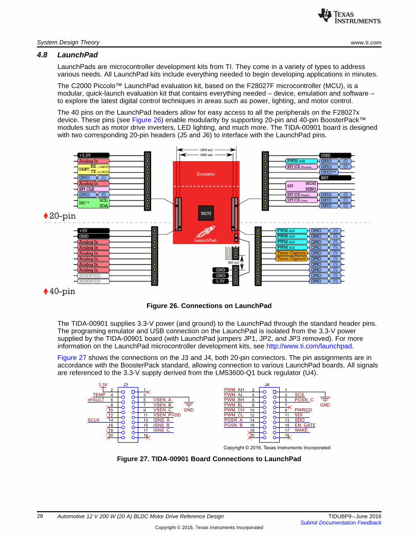
4.8 LaunchPadLaunchPads are microcontroller development kits from TI. They come in a variety of types to addressvarious needs. All LaunchPad kits include everything needed to begin developing applications in minutes.
The C2000 Piccolo™ LaunchPad evaluation kit, based on the F28027F microcontroller (MCU), is amodular, quick-launch evaluation kit that contains everything needed – device, emulation and software –to explore the latest digital control techniques in areas such as power, lighting, and motor control.
The 40 pins on the LaunchPad headers allow for easy access to all the peripherals on the F28027xdevice. These pins (see Figure 26) enable modularity by supporting 20-pin and 40-pin BoosterPack™modules such as motor drive inverters, LED lighting, and much more. The TIDA-00901 board is designedwith two corresponding 20-pin headers (J5 and J6) to interface with the LaunchPad pins.
Figure 26. Connections on LaunchPad
The TIDA-00901 supplies 3.3-V power (and ground) to the LaunchPad through the standard header pins.The programing emulator and USB connection on the LaunchPad is isolated from the 3.3-V powersupplied by the TIDA-00901 board (with LaunchPad jumpers JP1, JP2, and JP3 removed). For moreinformation on the LaunchPad microcontroller development kits, see http://www.ti.com/launchpad.
Figure 27 shows the connections on the J3 and J4, both 20-pin connectors. The pin assignments are inaccordance with the BoosterPack standard, allowing connection to various LaunchPad boards. All signalsare referenced to the 3.3-V supply derived from the LM53600-Q1 buck regulator (U4).
Figure 27. TIDA-00901 Board Connections to LaunchPad

www.ti.com Getting Started Hardware
29TIDUBP9–June 2016Submit Documentation Feedback
Copyright © 2016, Texas Instruments Incorporated
Automotive 12 V 200 W (20 A) BLDC Motor Drive Reference Design
The PWM signals are generated by the microcontroller, and connect with the DRV8305-Q1 gate driverchip. The HALL signals come from the optional motor position sensors, and connect to the microcontrollerfor sensored commutation. The feedback signals (voltage, current, and temperature) are scaled andfiltered by RC components, to reduce high-frequency noise. These filter components can be modified ifdesigners find specific noise frequencies which must be attenuated.
5 Getting Started HardwareIn order to fully demonstrate the TIDA-00901 design, several hardware components are required. Theseinclude:• The TIDA-00901 motor drive board• A LaunchPad with InstaSPIN-FOC-enabled microcontroller, such as the LAUNCHXL-F28027F• A brushless DC motor, with or without commutation sensors (e.g. Hall Effect sensors)• A 12-V power supply, capable of providing adequate current to power the selected motor• A computer with the software installed to control the system
5.1 Install LaunchPadThe TIDA-00901 board is designed to accommodate connection with an F28027F LaunchPad board. Theboard-to-board connections are made through two 20-pin headers, in accordance with theLaunchPad/BoosterPack development environment.
Before mounting the TIDA-00901 board on the LaunchPad, verify that the switches and jumpers on theLaunchPad are set correctly.
During operation with the TIDA-00901 board, the LaunchPad is powered from the 3.3V-supply generatedby the TIDA-00901 buck regulator. Therefore, the shunts on jumpers JP1, JP2, and JP3 on theLaunchPad board must be removed.There are additional switches on the Launchpad which must be set correctly; S1 (boot mode selection)and S4 (serial connectivity select).
The LaunchPad's microcontroller includes a boot ROM that performs some basic start-up checks andallows for the device to boot in many different ways. S1 is provided to allow users to easily configure thepins that the bootROM checks to make this decision whether to perform an emulation boot or a boot toflash. In general, all 3 switches on S1 must be in the ON position. More information about boot modeselection can be found in the TMS320x2802x Piccolo Boot ROM Reference Guide (SPRUFN6).
When S4 is in the up (ON) position, the Piccolo device's SCI is connected to the XDS100 and users areable to receive and send serial information from or to the board via the USB connection. When S4 is in thedown position, the Piccolo device's SCI is disconnected from the XDS100 and BoosterPacks.
NOTE: Use caution when mounting the LaunchPad to the TIDA-00901 board, as misalignment ofthe header pins during installation may cause damage.

Getting Started Hardware www.ti.com
30 TIDUBP9–June 2016Submit Documentation Feedback
Copyright © 2016, Texas Instruments Incorporated
Automotive 12 V 200 W (20 A) BLDC Motor Drive Reference Design
The TIDA-00901 board is designed to allow mounting on top of the LaunchPad board. The correctorientation of the TIDA-00901 board on the F28027F LaunchPad board is shown in Figure 28. Observethat the 3-position motor connector on the TIDA-00901 board is near the micro-USB connector on theLaunchPad board.
Figure 28. TIDA-00901 Board Installed on the F28027F LaunchPad
5.2 Power ConnectionFor operation, this design requires connection to a 12-V supply with current capability as dictated by themotor to be driven, typically in the range of several Amps. Connect leads to the 2-contact screw terminalblock on the side of the TIDA-00901 board. The ground screw terminal is labeled to indicate the properpolarity of the supply connection.
5.3 Motor ConnectionThe motor connections consist of the drive signals to the three-phase brushless DC motor, phase A,phase B, and phase C, as well as the optional Hall Effect sensor signals, and also the bias voltage forthose sensors.
5.3.1 Motor Phase ConnectionThe board is designed for a 3-phase brushless DC motor. The motor connections are suitable for a motorconfigured in either a Y or Δ configuration. The A and C phase voltages are marked next to thecorresponding terminals; terminal B is in the middle.
NOTE: The order of the phases is not critical, but that reversing any two phases will cause areversal in the motor direction.
Figure 29 shows the connections to the TIDA-00901 board and LaunchPad.

Motor phase connections
USB connection to computer
12-V power input
www.ti.com Getting Started Hardware
31TIDUBP9–June 2016Submit Documentation Feedback
Copyright © 2016, Texas Instruments Incorporated
Automotive 12 V 200 W (20 A) BLDC Motor Drive Reference Design
Figure 29. Board Connections
5.3.2 Motor Communication Feedback ConnectionThe board is designed to accept commutation feedback signals, such as Hall Effect sensors, from themotor. If these sensors are used, connect to the 5-position terminal block J5. A connection to the 3.3-Vsupply is included on J5, which can be used to bias the Hall effect sensors, if needed. In the case that asensor supply other than 3.3V is used, this can be applied to pin J5-5 from an external source, providedresistor R15 is removed from the TIDA-00901 board.

Getting Started Software www.ti.com
32 TIDUBP9–June 2016Submit Documentation Feedback
Copyright © 2016, Texas Instruments Incorporated
Automotive 12 V 200 W (20 A) BLDC Motor Drive Reference Design
6 Getting Started Software
6.1 Download and Install Code Composer Studio™Code Composer Studio™ (CCStudio) is an integrated development environment (IDE) for TexasInstruments (TI) embedded processor families. CCStudio comprises a suite of tools used to develop anddebug embedded applications. It includes compilers for each of TI's device families, source code editor,project build environment, debugger, profiler, simulators, real-time operating system and many otherfeatures. The intuitive IDE provides a single user interface taking you through each step of the applicationdevelopment flow. Familiar tools and interfaces allow users to get started faster than ever before and addfunctionality to their application thanks to sophisticated productivity tools. See the Code Composer Studioweb page at http://www.ti.com/tool/ccstudio for information on downloading the integrated developmentenvironment for the C2000 code.
6.2 Download and Install MotorWareThe TIDA-00901 board may be operated using a LaunchPad microcontroller development board. In thefollowing discussion, set-up using the C2000 LaunchPad LAUNCHXL-F28027F will be described. A linkmay be found in Section 9.
The TIDA-00901 board and connected LaunchPad board was tested using Texas Instruments’ MotorWaresoftware, with some additional files necessary to adapt to the specific hardware configuration of the TIDA-00901 board.
MotorWare is the software infrastructure and distribution mechanism for the InstaSPIN-FOC andInstaSPIN-MOTION motor control solutions. The software includes source code object oriented APIs forperipheral drivers and modules (including a freshly updated set of motor control functions). These APIsare used to build multiple InstaSPIN-FOC projects that demonstrate the different modes and capability,documented through the Projects and Lab User’s Guide.
The MotorWare software may be downloaded from http://www.ti.com/tool/MOTORWARE . Follow theinstallation instructions to install on your local computer.

www.ti.com Getting Started Software
33TIDUBP9–June 2016Submit Documentation Feedback
Copyright © 2016, Texas Instruments Incorporated
Automotive 12 V 200 W (20 A) BLDC Motor Drive Reference Design
6.3 Run the Example SoftwareThere are several lab projects in the MotorWare directory which can be used to exercise the TIDA-00901board. Lab project 2b uses the InstaSPIN motor identification algorithm to determine the key motorcharacteristics, and then uses sensorless commutation to drive the BLDC motor.
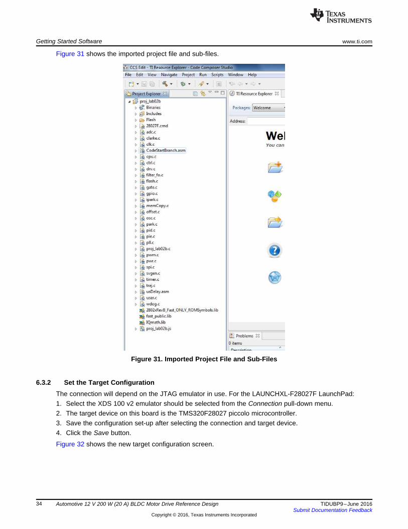
6.3.1 Import an Existing MotorWare Lab ProjectImport the existing project, for example proj_lab02b, from the MotorWare directory. In this instance, thereare two projects in the directory. Depending on how MotorWare is set up, there may be several projects inthe MotorWare directory to choose from.
Figure 30 shows the import existing CCS eclipse project screen.
Figure 30. Import Existing CCS Eclipse Project Screen
NOTE: This design works with other projects in the MotorWare libraries, but lab02b has all thefeatures needed to exercise the design as documented in this report.
Getting Started Software www.ti.com
34 TIDUBP9–June 2016Submit Documentation Feedback
Copyright © 2016, Texas Instruments Incorporated
Automotive 12 V 200 W (20 A) BLDC Motor Drive Reference Design
Figure 31 shows the imported project file and sub-files.
Figure 31. Imported Project File and Sub-Files
6.3.2 Set the Target ConfigurationThe connection will depend on the JTAG emulator in use. For the LAUNCHXL-F28027F LaunchPad:1. Select the XDS 100 v2 emulator should be selected from the Connection pull-down menu.2. The target device on this board is the TMS320F28027 piccolo microcontroller.3. Save the configuration set-up after selecting the connection and target device.4. Click the Save button.
Figure 32 shows the new target configuration screen.

www.ti.com Getting Started Software
35TIDUBP9–June 2016Submit Documentation Feedback
Copyright © 2016, Texas Instruments Incorporated
Automotive 12 V 200 W (20 A) BLDC Motor Drive Reference Design
Figure 32. New Target Configuration Screen
At this point, test the connection to the target. The connection to the target board may be verified.
Figure 33 shows the test connection window after completion of a successful test.
Figure 33. Test Connection Window After Completion of a Successful Test

Getting Started Software www.ti.com
36 TIDUBP9–June 2016Submit Documentation Feedback
Copyright © 2016, Texas Instruments Incorporated
Automotive 12 V 200 W (20 A) BLDC Motor Drive Reference Design
6.3.3 Adjust the Scale Factors in the user.h FileThe BOOSTXL-DRV8305EVM voltage sense circuits have a different attenuation factor than the TIDA-00901 board. Therefore, the maximum voltage setting should be modified in the user.h file (part of theMotorWare project) when using the TIDA-00901 board. Otherwise the PVDD supply voltage measurementand motor phase voltage measurements are not correct.1. In the file user.h, starting at line 90, change the USER_ADC_FULL_SCALE_VOLTAGE_V value:
//! \brief Defines the maximum voltage at the input to the AD converter
//! \brief The value that will be represented by the maximum ADC input (3.3V)and conversion (0FFFh)
//! \brief Hardware dependent, this should be based on the voltage sensing andscaling to the ADC input #define USER_ADC_FULL_SCALE_VOLTAGE_V (20.13) //
BOOSTXL-DRV8305EVM =44.30 V
// TIDA-00901 Board = 20.13V full-scale
2. The default setting of 47.14 Amps full-scale which corresponds to the BOOSTXL-DRV8305EVMhardware also works with the TIDA-00901 board. This value is set in the user.h file, and furtherdepends on the amplification setting for the current sense amplifiers (CSAs) in the DRV8305-Q1. If adifferent gain setting (or modified current sense circuitry) is of interest to best match a specficapplication, this full-scale value can be modified as shown in the following code fragment. In the fileuser.h, starting at line 105,//! \brief Defines the maximum current at the AD converter
//! \brief The value that will be represented by the maximum ADC input (3.3V)and conversion (0FFFh)
//! \brief Hardware dependent, this should be based on the current sensing andscaling to the ADC input
#define USER_ADC_FULL_SCALE_CURRENT_A (23.57) // BOOSTXL-DRV8305EVM = 47.14 A

www.ti.com Getting Started Software
37TIDUBP9–June 2016Submit Documentation Feedback
Copyright © 2016, Texas Instruments Incorporated
Automotive 12 V 200 W (20 A) BLDC Motor Drive Reference Design
6.3.4 Build the ProjectTo build the project:1. Click on the project name (for example, proj_lab02b) in the Project Explorer window to make sure that
the project is active.2. Click the hammer icon on the CCS Edit toolbar to build the project.3. If the project builds correctly, the message Build Finished is shown at the end of the text in the console
window.
NOTE: In case of errors during build or execution, there may be states where the project buildencounters problems due to previous build or execution. Performing a Clean build (selectClean under the Project Menu) rebuilds the project from a completely reset state.
Figure 34 shows the CCS Console window after successful build of the project.
Figure 34. CCS Console Window After Successful Build of the Project
6.3.5 Start a Debug Session With the ProjectStart a debug session by clicking the bug icon on the CCS Edit toolbar. The built project will bedownloaded to the LaunchPad microcontroller through the USB port and JTAG emulator.

Getting Started Software www.ti.com
38 TIDUBP9–June 2016Submit Documentation Feedback
Copyright © 2016, Texas Instruments Incorporated
Automotive 12 V 200 W (20 A) BLDC Motor Drive Reference Design
6.3.6 Run the ProjectTo run the project:1. Click the green Run/Resume icon in the CCS debug toolbar to run the project.2. Click the clock icon in the CCS debug toolbar to enable Silicion Real-Time Mode.3. Open the Expressions tab which is populated with the motor variable expression, as shown in
Figure 35.
Figure 35. Expressions Window in the Debug View of CCS, Program Running, Drive Not Enabled
6.3.7 Enable the SystemTo enable the system:1. Click the value field and enter a 1 to set the Flag_enableSys to 1.2. At this point the operation of the system may be verified. Observe that the 12-V supply voltage is
correctly monitored.3. If required, right-click inside the value field.4. Select the Q values and 24 to change the expression VdcBus_kV to Q-Value(24).5. Verify that the value for VdcBus_kV corresponds to the DC supply voltage.
Figure 36 shows that the supply voltage is 12.17 V.
If the VdcBus_kV value does not correspond to the input voltage on VBATT, check that the voltage gain inUser.h is correctly set, as discussed in Section 6.3.3.

www.ti.com Getting Started Software
39TIDUBP9–June 2016Submit Documentation Feedback
Copyright © 2016, Texas Instruments Incorporated
Automotive 12 V 200 W (20 A) BLDC Motor Drive Reference Design
Figure 36. Expressions Window in the Debug View of CCS, Program Running, and Drive Enabled
6.3.8 Identify the Motor ParametersClick inside the value field and enter 1 to set the Flag_Run_Identify to 1. The motor is driven with smalland large motions, drawing up to several Amps. During the identification procedure, the motor statorwinding resistance Rs_Ohm variable is estimated, as well as the winding inductance Lsd_H and Lsq_H,and the flux Flux_VpHz. The estimated values for each are updated in the Expressions window,highlighted in yellow after each update.
shows the motor winding resistance is 84-mΩ, and the winding inductance is 0.64 mH.
Figure 37. Expressions Window in the Debug View of CCS, During Motor Identification

Getting Started Software www.ti.com
40 TIDUBP9–June 2016Submit Documentation Feedback
Copyright © 2016, Texas Instruments Incorporated
Automotive 12 V 200 W (20 A) BLDC Motor Drive Reference Design
6.3.9 Operate in Speed Control ModeWhen the motor has been successfully identified, the Flag_Run_Identify is reset to 0.
At that point:1. Again, click inside the value field and enter 1 to set the Flag_Run_Identify to 1.
This allows the system to operate with the motor parameters already determined. After a moment, themotor begins to spin at the speed set by the SpeedRef_krpm parameter value.
2. Click inside the value field of SpeedRef_krpf and enter a new value (in kRPM) to change the commandspeed.
3. Click inside the value field of MaxAccel_krpmps and enter a new value (in kRPM per second) tochange the acceleration.
NOTE: The speed reference may be either positive or negative, affecting whether the motor rotatingis clockwise or counterclockwise.
Figure 38 shows the expressions window, motor speed 500 RPM (left) and –400 RPM (right).
Figure 38. Expressions Window, Motor Speed 500 RPM (left) and –400 RPM (right)
6.3.10 Operate With InstaSPIN Universal GUI to Adjust DRV8305-Q1 ParametersTo have easy access to the DRV8305-Q1 motor drive parameters, the board may also be operated usingthe InstaSPIN_F28027F_UNIVERSAL graphical user interface (GUI). For information about this GUI, seehttp://www.ti.com/tool/INSTASPINUNIVERSALGUI.
The InstaSPIN Universal GUI allows you to instrument bound variables for each compiled MotorWareproject (.out) on the Piccolo MCU. Use CCStudio to compile a MotorWare project into a .out that may beloaded onto the Piccolo MCU. Select the MotorWare project that meets your application requirements.See the InstaSPIN-FOC™ and Insta-SPIN-MOTION™ User's Guide (SPRUHJ1) for a list of availableprojects. The user.h file specifies the settings for your motor. Make sure that the appropriate settings areselected in the user.h, and that the file is saved before building the project as mentioned in Section 6.3.3.
To install:1. Rename the compiled MotorWare project (the binary, for example proj_lab2b.out, as shown in
Figure 39) to appProgram.out.

www.ti.com Getting Started Software
41TIDUBP9–June 2016Submit Documentation Feedback
Copyright © 2016, Texas Instruments Incorporated
Automotive 12 V 200 W (20 A) BLDC Motor Drive Reference Design
2. Copy the file to the appropriate webapp folder, in this case InstaSPIN_F2802xF_UNIVERSAL, typicallyunder C:\ti\guicomposer\webapps (depending on how MotorWare was installed).
Figure 39. Directory Path for .out File for Lab_2b
3. Run the executable from the webapp folder: InstaSPIN_UNIVERSAL.exe or by starting the MotorWareapplication
4. Select Run Universal GUI under the Piccolo F28027F >> GUI directory, as shown in Figure 40.
Figure 40. Universal GUI Application Entry Point
During the GUI launch, the USB link to the LaunchPad emulator is initialized and connected, theassociated firmware is flashed into the LaunchPad, and the C2000 program is executed. Figure 41shows the configuration tab of a successful GUI launch.
Figure 41. Configuration Tab of a Successful GUI Launch
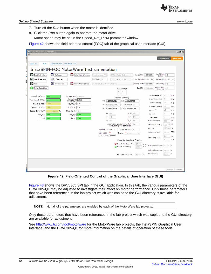
When the GUI is running, a screen with several tabs is available for controlling both the motoroperation and the control parameters resident in the DRV8305-Q1 registers. Figure 42 shows theField-Oriented Control tab which has options for setting the state of the motor drive, and for enteringspeed control targets.
5. Click the Enable System button to command operation of the motor.6. Click the Run button.
The system uses InstaSPIN to identify the motor parameters.
Getting Started Software www.ti.com
42 TIDUBP9–June 2016Submit Documentation Feedback
Copyright © 2016, Texas Instruments Incorporated
Automotive 12 V 200 W (20 A) BLDC Motor Drive Reference Design
7. Turn off the Run button when the motor is identified.8. Click the Run button again to operate the motor drive.
Motor speed may be set in the Speed_Ref_RPM parameter window.
Figure 42 shows the field-oriented control (FOC) tab of the graphical user interface (GUI).
Figure 42. Field-Oriented Control of the Graphical User Interface (GUI)
Figure 43 shows the DRV8305 SPI tab in the GUI application. In this tab, the various parameters of theDRV8305-Q1 may be adjusted to investigate their affect on motor performance. Only those parametersthat have been referenced in the lab project which was copied to the GUI directory is available foradjustment.
NOTE: Not all of the parameters are enabled by each of the MotorWare lab projects.
Only those parameters that have been referenced in the lab project which was copied to the GUI directoryare available for adjustment.
See http://www.ti.com/tool/motorware for the MotorWare lab projects, the InstaSPIN Graphical UserInterface, and the DRV8305-Q1 for more information on the details of operation of these tools.

www.ti.com Getting Started Software
43TIDUBP9–June 2016Submit Documentation Feedback
Copyright © 2016, Texas Instruments Incorporated
Automotive 12 V 200 W (20 A) BLDC Motor Drive Reference Design
Figure 43. DRV8305 SPI Tab in the GUI

PVDD Input Voltage (V)
3.3
-V S
up
ply
Vo
lta
ge
(V
)
0 2 4 6 8 10 12 140
0.5
1
1.5
2
2.5
3
3.5
D003
Testing www.ti.com
44 TIDUBP9–June 2016Submit Documentation Feedback
Copyright © 2016, Texas Instruments Incorporated
Automotive 12 V 200 W (20 A) BLDC Motor Drive Reference Design
7 TestingThe following sections show the test data which characterize the design. These results indicate typicalperformance with equipment similar to that expected in the intended applications.
7.1 Power Supplies
7.1.1 12-V Supply CurrentTable 6 lists the supply current under various conditions with a 12-V (nominal supply). A motor was notconnected to the board for these measurements.
Table 6. Supply Current Under Various Operating Conditions
CONDITION CURRENT (mA)No load (no LaunchPad) 8
With LaunchPad Installed (C2000 idle) 33With LaunchPad Installed (C2000 running, DRV8305 disabled) 66With LaunchPad installed (C2000 running, DRV8305 enabled) 68
7.1.2 12-V Supply Range of OperationThe design is intended for operation with a range of voltage on the 12-V automotive battery supply.Figure 44 shows the measured output of the 3.3-V supply for a positive range of input voltage on J1 withno LaunchPad installed. The curve indicates operation beginning at about 5 V, where the 3.3-V regulatorcircuit begins to operate.
Figure 44. 3.3-V Regulator Output Voltage vs Positive Input Voltage on PVDD

PVDD Battery Voltage (V)
Cur
rent
(m
A)
-18 -16 -14 -12 -10 -8 -6 -4 -2 0-3.5
-3
-2.5
-2
-1.5
-1
-0.5
0
D004
www.ti.com Testing
45TIDUBP9–June 2016Submit Documentation Feedback
Copyright © 2016, Texas Instruments Incorporated
Automotive 12 V 200 W (20 A) BLDC Motor Drive Reference Design
The reverse-battery performance is shown in Figure 45. Observe that the reverse current is primarily dueto the path through R2 through the base-emitter junction of Q1 and D1 (refer to Figure 9). The collector ofQ1 pulls the gate of Q8 below the threshold point, keeping Q8 in the off state.
Figure 45. Input Current vs Negative Input Voltage on PVDD
7.1.3 3.3-V Buck Turn-On TransitionsAlthough not a key parameter for most applications, the turn-on time after application of battery power is ofinterest. The plots in Figure 46 and Figure 47 show that the 3.3-V buck supply is regulating at 3.3 V within4 ms of the battery voltage being applied.
Figure 46. 3.3-V Buck Supply Turn-On During VBAT Supply Transition to 12 V
External Load Current on 3.3-V Supply (mA)
Sup
ply
Cur
rent
(m
A)
Reg
ulat
or O
utpu
t (V
)
0 50 100 150 200 250 300 350 4000 3.22
20 3.24
40 3.26
60 3.28
80 3.3
100 3.32
120 3.34
140 3.36
D005
Testing www.ti.com
46 TIDUBP9–June 2016Submit Documentation Feedback
Copyright © 2016, Texas Instruments Incorporated
Automotive 12 V 200 W (20 A) BLDC Motor Drive Reference Design
Figure 47. 3.3-V Buck Supply Turn-On during VBAT Supply Transition to 6 V
7.1.4 3.3-V Buck Load RegulationThe 3.3-V regulator is designed to supply current to the on-board temperature sensor, Hall Effectinterface, and LED indicators, as well as the off-board microcontroller. The regulator is designed to supplyup to 350 mA of current to the off-board controller; this is more than sufficient for a typical device such asthe C2000 real-time microcontroller, as implemented on the C28027F LaunchPad.
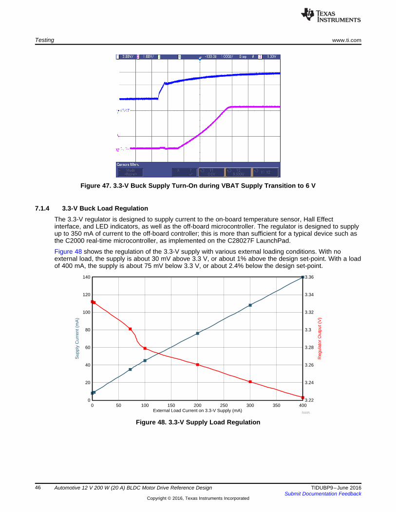
Figure 48 shows the regulation of the 3.3-V supply with various external loading conditions. With noexternal load, the supply is about 30 mV above 3.3 V, or about 1% above the design set-point. With a loadof 400 mA, the supply is about 75 mV below 3.3 V, or about 2.4% below the design set-point.
Figure 48. 3.3-V Supply Load Regulation

www.ti.com Testing
47TIDUBP9–June 2016Submit Documentation Feedback
Copyright © 2016, Texas Instruments Incorporated
Automotive 12 V 200 W (20 A) BLDC Motor Drive Reference Design
7.1.5 3.3-V Buck EfficiencyThe efficiency of the 3.3-V regulator is determined by measuring the power delivered to an external loadon the 3.3-V supply and the 12-V power supplied to the board. Based on the incremental power suppliedto the external load, and the incremental power supplied by the 12-V supply, the overall 3.3-V regulatorefficiency is measured as approximately 81%.
Table 7 lists the efficiency measurements for the 3.3-V regulator.
Table 7. Efficiency Measurements for the 3.3-V Regulator
EXTERNALLOAD (mA)
12-V SUPPLY(mA)
REGULATOROUTPUT
INPUTPOWER OUTPUT POWER 3.3-V POWER
EFFICIENCY0 8 3.332 96 0
3.4 9 3.331 108 11.3254 94%72 35 3.301 420 237.672 73%
100 45 3.279 540 327.9 75%200 76 3.2605 912 652.1 87%300 108 3.241 1,296 972.3 83%400 140 3.223 1,680 1,289.2 83%
OVERALL: 81%
7.1.6 Input Power FilteringThe plots shown in Figure 49 and Figure 50 were taken with the ElectroCraft motor rotating at 100 RPM,with another motor connected as a braking generator load and 3 parallel 33-Ω resistors on each phase,loading the generator. The left plot is measured at PVDD test point. The right plot is measured at the J1-2power input for VBAT, showing the effect of the filtering, which has attenuated the maximum peak by 27dB, or an attenuation factor of 23.
Figure 49. Without Input Power Filter, ShowingAttenuation of PWM Harmonics
Figure 50. With Input Power Filter, Showing Attenuationof PWM Harmonics
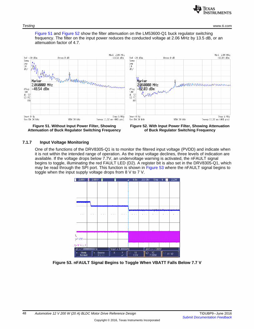
Testing www.ti.com
48 TIDUBP9–June 2016Submit Documentation Feedback
Copyright © 2016, Texas Instruments Incorporated
Automotive 12 V 200 W (20 A) BLDC Motor Drive Reference Design
Figure 51 and Figure 52 show the filter attenuation on the LM53600-Q1 buck regulator switchingfrequency. The filter on the input power reduces the conducted voltage at 2.06 MHz by 13.5 dB, or anattenuation factor of 4.7.
Figure 51. Without Input Power Filter, ShowingAttenuation of Buck Regulator Switching Frequency
Figure 52. With Input Power Filter, Showing Attenuationof Buck Regulator Switching Frequency
7.1.7 Input Voltage MonitoringOne of the functions of the DRV8305-Q1 is to monitor the filtered input voltage (PVDD) and indicate whenit is not within the intended range of operation. As the input voltage declines, three levels of indication areavailable. If the voltage drops below 7.7V, an undervoltage warning is activated, the nFAULT signalbegins to toggle, illuminating the red FAULT LED (D2). A register bit is also set in the DRV8305-Q1, whichmay be read through the SPI port. This function is shown in Figure 53 where the nFAULT signal begins totoggle when the input supply voltage drops from 8 V to 7 V.
Figure 53. nFAULT Signal Begins to Toggle When VBATT Falls Below 7.7 V

www.ti.com Testing
49TIDUBP9–June 2016Submit Documentation Feedback
Copyright © 2016, Texas Instruments Incorporated
Automotive 12 V 200 W (20 A) BLDC Motor Drive Reference Design
7.2 Motor Operation
7.2.1 Motor Drive SignalsThe overall motor drive function of the TIDA-00901 board is shown in Figure 54. Here, the six PWMcommands from the C2000 LaunchPad, which are the input signals to the TIDA-00901 board, are shownin light blue at the bottom of the oscilloscope plots. Note that each of the three pairs of signals iscomprised of complementary commands for the high-side and low-side gate drivers of each motor phase.(As discussed later, the dead-time between complementary transitions can be set to a minimum, as theDRV8305-Q1 has integrated programmable dead-time control.) The three motor phase voltages areshown in color; these are the main outputs from the TIDA-00901 board. Note that the high and lowsegments of each motor phase are roughly aligned with the corresponding PWM input commands. Thetime shift between command and phase voltage is due to the charge-up time and transition slew rate ofthe drive FETs, as well as the dead-time inserted between complementary transitions. The DRV8305-Q1allows users to adjust the motor drive parameters in terms of both time shift and slew rate byprogramming the internal registers through SPI transactions.
Figure 54. Inputs and Outputs During Normal Operation, 12-V Supply, 45 kHz PWM Frequency, No-LoadMotor
7.2.2 Motor Operation Test SetupThis design was tested with various 3-phase BLDC motors. Brief specifications for these are listed in theappendix. To provide a known load for the motor, a dynamometer was coupled to the motor shaft.Figure 55 shows one such motor coupled to the dynamometer, with the boards being tested driving themotor.
Several items must be noted related to dynamometer testing:• The motor may be rotating at high speeds, and may have sufficient torque to cause damage or injury.
Care must be taken to keep clothing, tools, and more away from the rotating shaft during testing.• Alignment of the motor shaft to the dynamometer shaft is important for safe operation and for accurate
measurement of the motor performance. Misalignment may lead to damage of the coupling or incorrecttorque readings.
• Rapid changes of the motor speed may lead to overvoltage generated by the motor. Be aware that thegenerated voltage may exceed the voltage set-point of the 12-V supply.
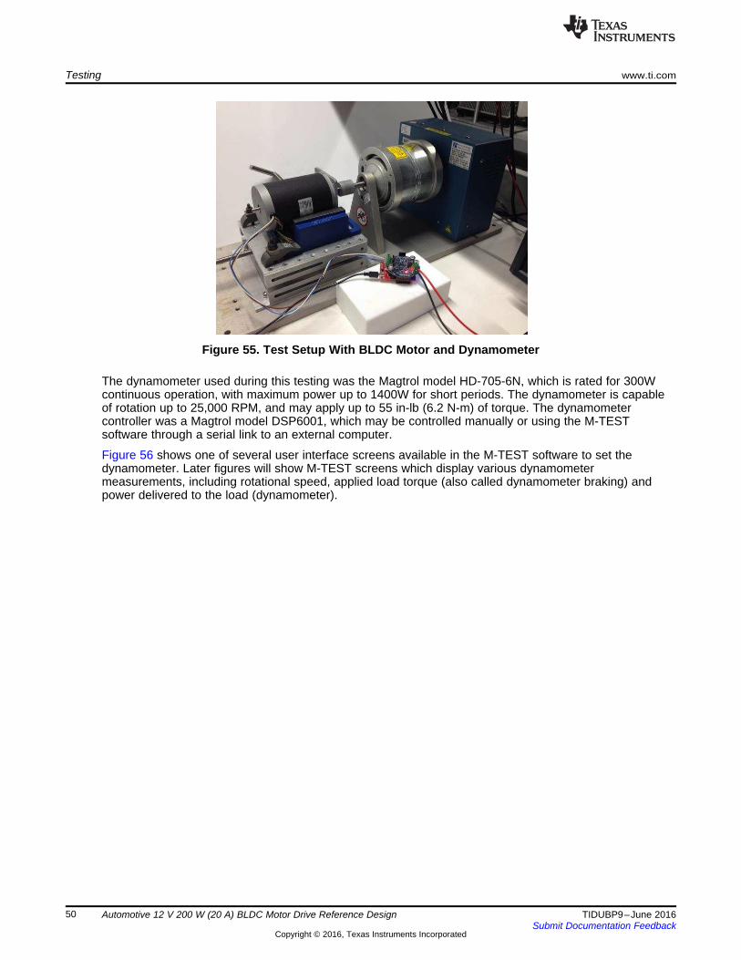
Testing www.ti.com
50 TIDUBP9–June 2016Submit Documentation Feedback
Copyright © 2016, Texas Instruments Incorporated
Automotive 12 V 200 W (20 A) BLDC Motor Drive Reference Design
Figure 55. Test Setup With BLDC Motor and Dynamometer
The dynamometer used during this testing was the Magtrol model HD-705-6N, which is rated for 300Wcontinuous operation, with maximum power up to 1400W for short periods. The dynamometer is capableof rotation up to 25,000 RPM, and may apply up to 55 in-lb (6.2 N-m) of torque. The dynamometercontroller was a Magtrol model DSP6001, which may be controlled manually or using the M-TESTsoftware through a serial link to an external computer.
Figure 56 shows one of several user interface screens available in the M-TEST software to set thedynamometer. Later figures will show M-TEST screens which display various dynamometermeasurements, including rotational speed, applied load torque (also called dynamometer braking) andpower delivered to the load (dynamometer).
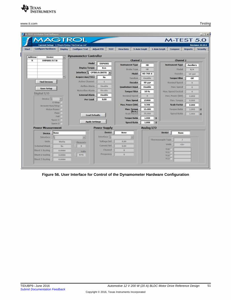
www.ti.com Testing
51TIDUBP9–June 2016Submit Documentation Feedback
Copyright © 2016, Texas Instruments Incorporated
Automotive 12 V 200 W (20 A) BLDC Motor Drive Reference Design
Figure 56. User Interface for Control of the Dynamometer Hardware Configuration

Motor Speed (RPM)
Sup
ply
Cur
rent
(m
A)
0 250 500 750 1000 1250 1500 1750 2000 2250 25000
200
400
600
800
1000
1200
1400
1600
1800
2000
2200
D007
8 V12 V18 V
Motor Speed (RPM)
Sup
ply
Cur
rent
(m
A)
0 250 500 750 1000 1250 1500 1750 2000 2250 250050
100
150
200
250
300
350
400
450
500
550
600
D006
8 V12 V18 V
Testing www.ti.com
52 TIDUBP9–June 2016Submit Documentation Feedback
Copyright © 2016, Texas Instruments Incorporated
Automotive 12 V 200 W (20 A) BLDC Motor Drive Reference Design
7.2.3 Motor No-Load OperationThe 12-V automotive battery supply is expected to vary in real-world applications. This design mustmaintain control of the motor over a range of at least 8 V to 18 V, but the motor drive performance isaffected by the supply voltage.• At any given supply voltage, the current required to maintain a specific speed varies more or less
directly with the speed.• Assuming a constant load, the maximum attainable speed increases as the applied supply voltage
increases.• At any given speed, the motor current varies inversely with the applied voltage, assuming a constant
load.
The plots shown in Figure 57 show these relationships for the IHN06576 motor. Observe that thesemeasurements were with no dynamometer attached. The maximum no-load speed for each supply voltageis indicated by the endpoint of the corresponding line.
Unless otherwise specified in later sections, the motor supply for all remaining measurements was set tothe nominal value of 12 V.
Figure 57. Motor No-Load Current vs Speed for Various Supply Voltages
7.2.4 Motor Operation With HVAC Blower WheelThe plots in Figure 58 show these relationships for the IHN06576 motor with a six-inch (150 mm) blowerwheel. The maximum speed for each supply voltage is indicated by the endpoint of the corresponding line.
Figure 58. Motor Operation With HVAC Blower Wheel
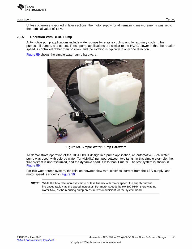
www.ti.com Testing
53TIDUBP9–June 2016Submit Documentation Feedback
Copyright © 2016, Texas Instruments Incorporated
Automotive 12 V 200 W (20 A) BLDC Motor Drive Reference Design
Unless otherwise specified in later sections, the motor supply for all remaining measurements was set tothe nominal value of 12 V.
7.2.5 Operation With BLDC PumpAutomotive pump applications include water pumps for engine cooling and for auxiliary cooling, fuelpumps, oil pumps, and others. These pump applications are similar to the HVAC blower in that the rotationspeed is controlled rather than position, and the rotation is typically in only one direction.
Figure 59 shows the simple water pump hardware.
Figure 59. Simple Water Pump Hardware
To demonstrate operation of the TIDA-00901 design in a pump application, an automotive 50-W waterpump was used, with colored water (for visibility) pumped between two tanks. In this simple example, thefluid system is unpressurized, and the dynamic head is less than 1 meter. The test system is shown inFigure 59.
For this water pump system, the relation between flow rate, electrical current from the 12-V supply, andmotor speed is shown in Figure 59.
NOTE: While the flow rate increases more or less linearly with motor speed, the supply currentincreases rapidly as the speed increases. For motor speeds below 500 RPM, there was nowater flow, as the resulting pump pressure was insufficient for the system head.
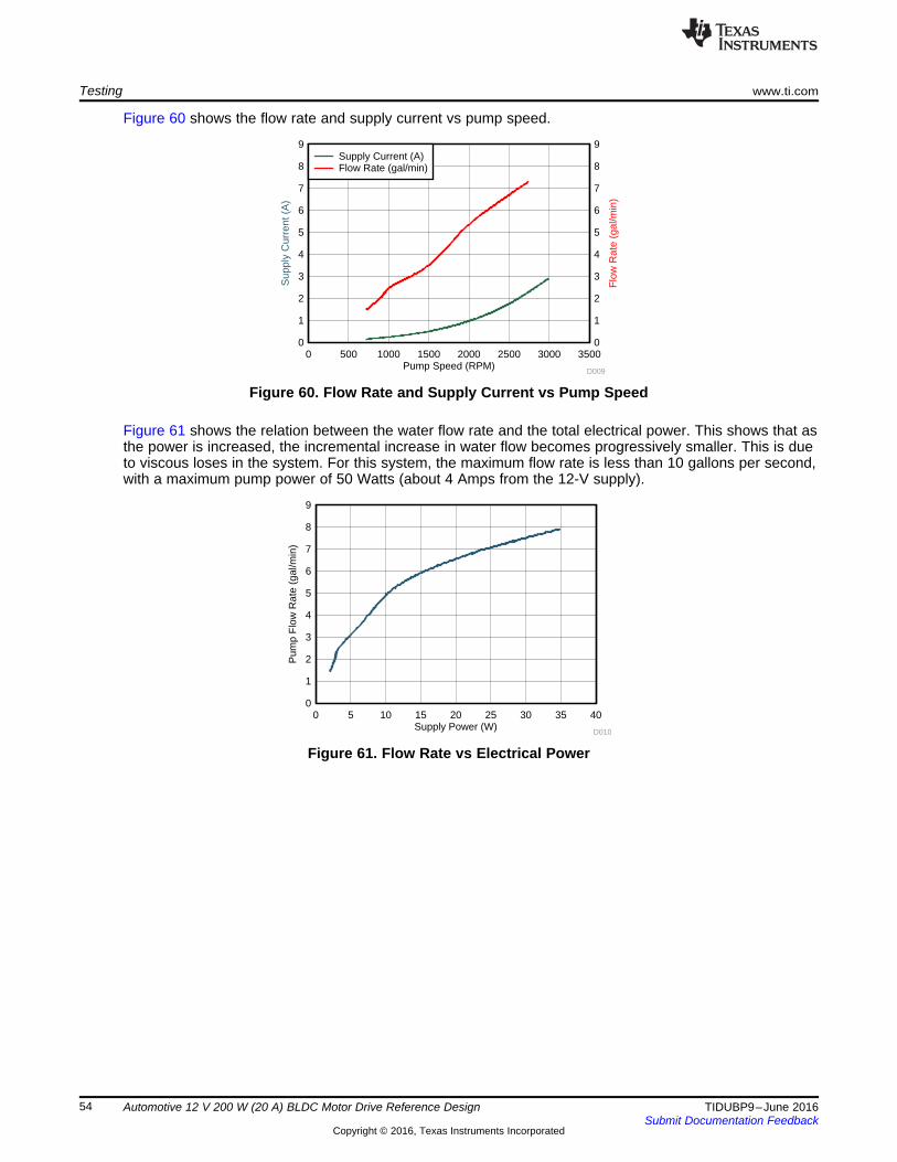
Supply Power (W)
Pum
p F
low
Rat
e (g
al/m
in)
0 5 10 15 20 25 30 35 400
1
2
3
4
5
6
7
8
9
D010
Pump Speed (RPM)
Sup
ply
Cur
rent
(A
)
Flo
w R
ate
(gal
/min
)
0 500 1000 1500 2000 2500 3000 35000 0
1 1
2 2
3 3
4 4
5 5
6 6
7 7
8 8
9 9
D009
Supply Current (A)Flow Rate (gal/min)
Testing www.ti.com
54 TIDUBP9–June 2016Submit Documentation Feedback
Copyright © 2016, Texas Instruments Incorporated
Automotive 12 V 200 W (20 A) BLDC Motor Drive Reference Design
Figure 60 shows the flow rate and supply current vs pump speed.
Figure 60. Flow Rate and Supply Current vs Pump Speed
Figure 61 shows the relation between the water flow rate and the total electrical power. This shows that asthe power is increased, the incremental increase in water flow becomes progressively smaller. This is dueto viscous loses in the system. For this system, the maximum flow rate is less than 10 gallons per second,with a maximum pump power of 50 Watts (about 4 Amps from the 12-V supply).
Figure 61. Flow Rate vs Electrical Power
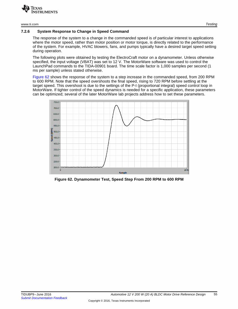
www.ti.com Testing
55TIDUBP9–June 2016Submit Documentation Feedback
Copyright © 2016, Texas Instruments Incorporated
Automotive 12 V 200 W (20 A) BLDC Motor Drive Reference Design
7.2.6 System Response to Change in Speed CommandThe response of the system to a change in the commanded speed is of particular interest to applicationswhere the motor speed, rather than motor position or motor torque, is directly related to the performanceof the system. For example, HVAC blowers, fans, and pumps typically have a desired target speed settingduring operation.
The following plots were obtained by testing the ElectroCraft motor on a dynamometer. Unless otherwisespecified, the input voltage (VBAT) was set to 12 V. The MotorWare software was used to control theLaunchPad commands to the TIDA-00901 board. The time scale factor is 1,000 samples per second (1ms per sample) unless stated otherwise.
Figure 62 shows the response of the system to a step increase in the commanded speed, from 200 RPMto 600 RPM. Note that the speed overshoots the final speed, rising to 720 RPM before settling at thetarget speed. This overshoot is due to the settings of the P-I (proportional integral) speed control loop inMotorWare. If tighter control of the speed dynamics is needed for a specific application, these parameterscan be optimized; several of the later MotorWare lab projects address how to set these parameters.
Figure 62. Dynamometer Test, Speed Step From 200 RPM to 600 RPM

Testing www.ti.com
56 TIDUBP9–June 2016Submit Documentation Feedback
Copyright © 2016, Texas Instruments Incorporated
Automotive 12 V 200 W (20 A) BLDC Motor Drive Reference Design
Figure 63 shows the system response to a step increase in motor speed from 600 RPM to 1,000 RPM.Again the overshoot in the response is evident, with a maximum overshoot value of almost 40% of thecommanded speed increase. The speed settles to within a few percent of the commanded rate in lessthan a second.
Figure 63. Dynamometer Test, Speed Step From 600 RPM to 1,000 RPM
Figure 64 shows the system dynamic response to a step decrease in commanded rate from 1000 RPM to200 RPM. The overshoot is less pronounced, but still evident. The motor settles into the new commandedspeed after a few cycles of ringing.
Figure 64. Dynamometer Test, Speed Step From 1,000 RPM to 200 RPM
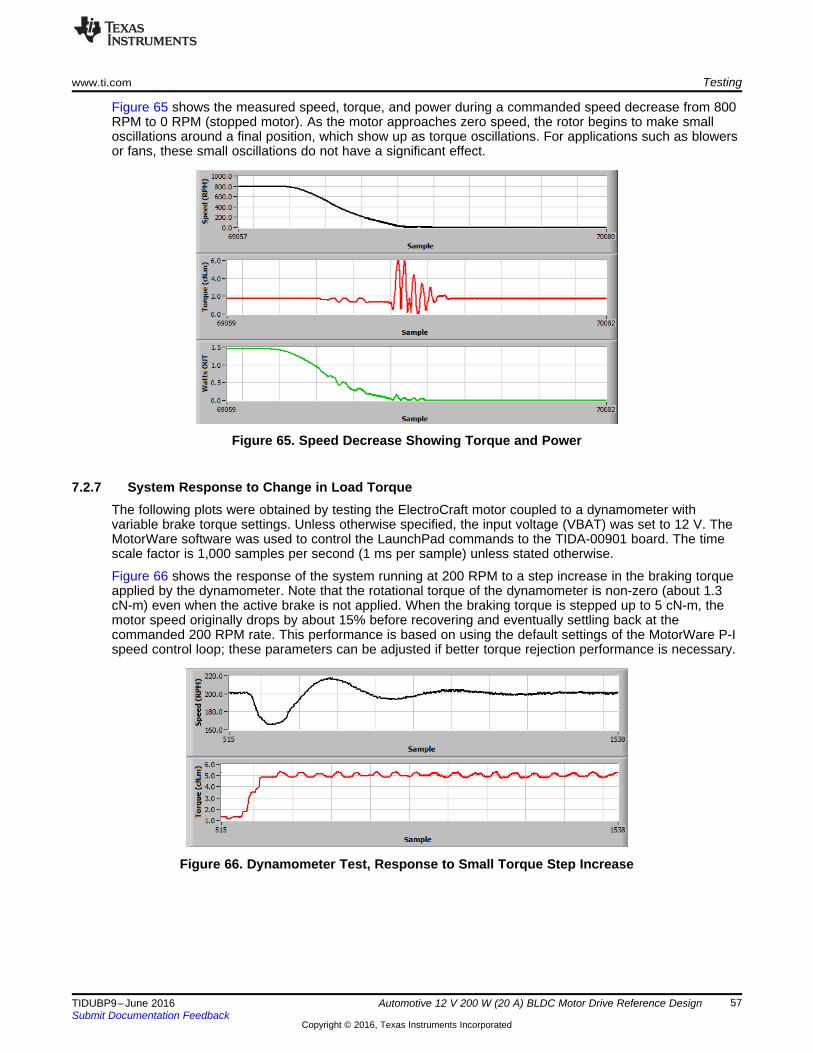
www.ti.com Testing
57TIDUBP9–June 2016Submit Documentation Feedback
Copyright © 2016, Texas Instruments Incorporated
Automotive 12 V 200 W (20 A) BLDC Motor Drive Reference Design
Figure 65 shows the measured speed, torque, and power during a commanded speed decrease from 800RPM to 0 RPM (stopped motor). As the motor approaches zero speed, the rotor begins to make smalloscillations around a final position, which show up as torque oscillations. For applications such as blowersor fans, these small oscillations do not have a significant effect.
Figure 65. Speed Decrease Showing Torque and Power
7.2.7 System Response to Change in Load TorqueThe following plots were obtained by testing the ElectroCraft motor coupled to a dynamometer withvariable brake torque settings. Unless otherwise specified, the input voltage (VBAT) was set to 12 V. TheMotorWare software was used to control the LaunchPad commands to the TIDA-00901 board. The timescale factor is 1,000 samples per second (1 ms per sample) unless stated otherwise.
Figure 66 shows the response of the system running at 200 RPM to a step increase in the braking torqueapplied by the dynamometer. Note that the rotational torque of the dynamometer is non-zero (about 1.3cN-m) even when the active brake is not applied. When the braking torque is stepped up to 5 cN-m, themotor speed originally drops by about 15% before recovering and eventually settling back at thecommanded 200 RPM rate. This performance is based on using the default settings of the MotorWare P-Ispeed control loop; these parameters can be adjusted if better torque rejection performance is necessary.
Figure 66. Dynamometer Test, Response to Small Torque Step Increase
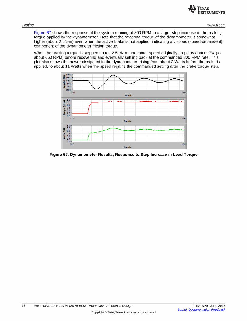
Testing www.ti.com
58 TIDUBP9–June 2016Submit Documentation Feedback
Copyright © 2016, Texas Instruments Incorporated
Automotive 12 V 200 W (20 A) BLDC Motor Drive Reference Design
Figure 67 shows the response of the system running at 800 RPM to a larger step increase in the brakingtorque applied by the dynamometer. Note that the rotational torque of the dynamometer is somewhathigher (about 2 cN-m) even when the active brake is not applied, indicating a viscous (speed-dependent)component of the dynamometer friction torque.
When the braking torque is stepped up to 12.5 cN-m, the motor speed originally drops by about 17% (toabout 660 RPM) before recovering and eventually settling back at the commanded 800 RPM rate. Thisplot also shows the power dissipated in the dynamometer, rising from about 2 Watts before the brake isapplied, to about 11 Watts when the speed regains the commanded setting after the brake torque step.
Figure 67. Dynamometer Results, Response to Step Increase in Load Torque
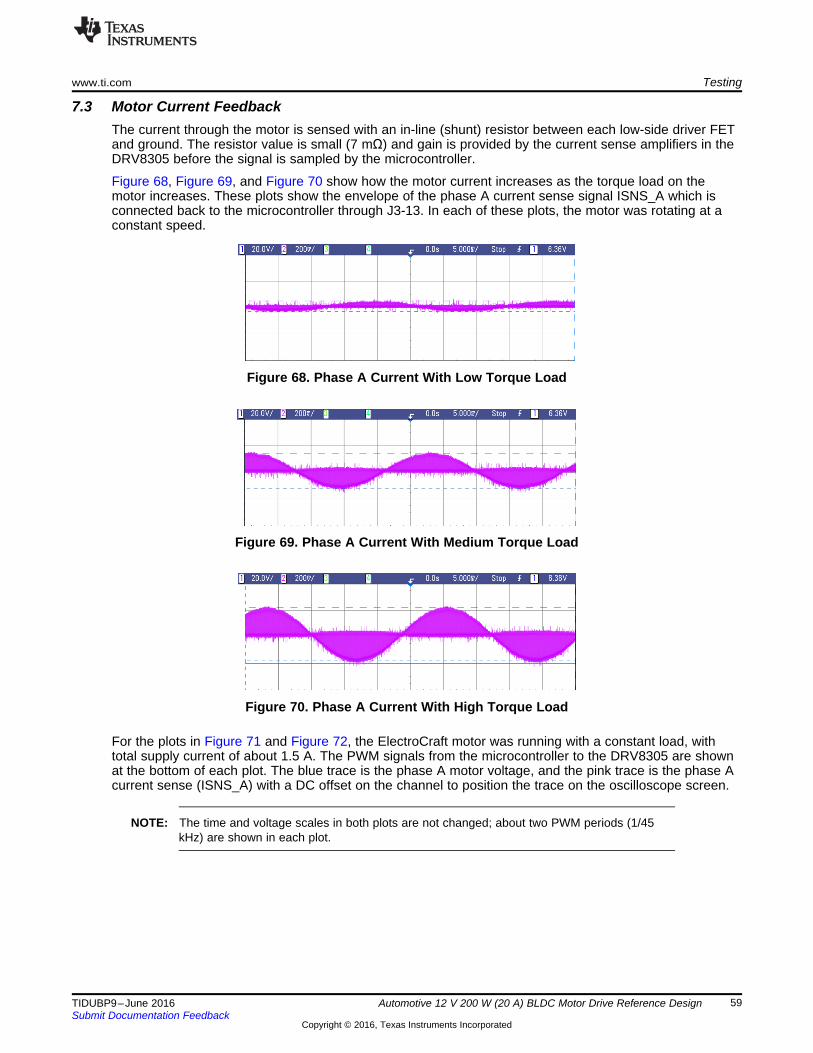
www.ti.com Testing
59TIDUBP9–June 2016Submit Documentation Feedback
Copyright © 2016, Texas Instruments Incorporated
Automotive 12 V 200 W (20 A) BLDC Motor Drive Reference Design
7.3 Motor Current FeedbackThe current through the motor is sensed with an in-line (shunt) resistor between each low-side driver FETand ground. The resistor value is small (7 mΩ) and gain is provided by the current sense amplifiers in theDRV8305 before the signal is sampled by the microcontroller.
Figure 68, Figure 69, and Figure 70 show how the motor current increases as the torque load on themotor increases. These plots show the envelope of the phase A current sense signal ISNS_A which isconnected back to the microcontroller through J3-13. In each of these plots, the motor was rotating at aconstant speed.
Figure 68. Phase A Current With Low Torque Load
Figure 69. Phase A Current With Medium Torque Load
Figure 70. Phase A Current With High Torque Load
For the plots in Figure 71 and Figure 72, the ElectroCraft motor was running with a constant load, withtotal supply current of about 1.5 A. The PWM signals from the microcontroller to the DRV8305 are shownat the bottom of each plot. The blue trace is the phase A motor voltage, and the pink trace is the phase Acurrent sense (ISNS_A) with a DC offset on the channel to position the trace on the oscilloscope screen.
NOTE: The time and voltage scales in both plots are not changed; about two PWM periods (1/45kHz) are shown in each plot.

Testing www.ti.com
60 TIDUBP9–June 2016Submit Documentation Feedback
Copyright © 2016, Texas Instruments Incorporated
Automotive 12 V 200 W (20 A) BLDC Motor Drive Reference Design
Figure 71. Phase A Voltage High Figure 72. Phase A Voltage Low
In Figure 71, the phase A voltage (blue) is high for most of the PWM period, and the phase A current isflowing from the board terminal (J2-3) into the motor phase A winding. During the majority of the PWMperiod, the phase A high-side FET (Q2) is on in response to the high level on PWM_AH. While Q2 is on,the phase A low-side FET (Q5) is off, and the current sense voltage corresponds to the zero current level.For the short time that the motor phase A voltage is low, the A-phase low-side FET is on, and current isflowing from ground through the sense resistor and out to the motor phase. Thus the pink ISNS_Awaveform goes above the dashed zero current line, indicating a current from ground to Q5 through R3, thephase A current sense resistor. (The inverting terminal of the current sense amplifier is on the motor sideof R3, and the non-inverting terminal is at ground potential.)
In Figure 72, the phase A voltage (blue) is high for a small fraction of the PWM period, and phase Acurrent is flowing from the motor winding into the phase A terminal. For the short time when the phase Avoltage is high, the A phase high-side FET (Q2) is on. During this time, the A phase low-side FET (Q5) isoff, and the current through the A phase current sense resistor (R3) is zero. During the longer time in theright plot, the phase A voltage is zero, indicating the A phase low-side FET (Q5) is on, and the currentthrough R3 is from the motor towards ground, producing a current sense reading (pink) below the dashedzero current line.
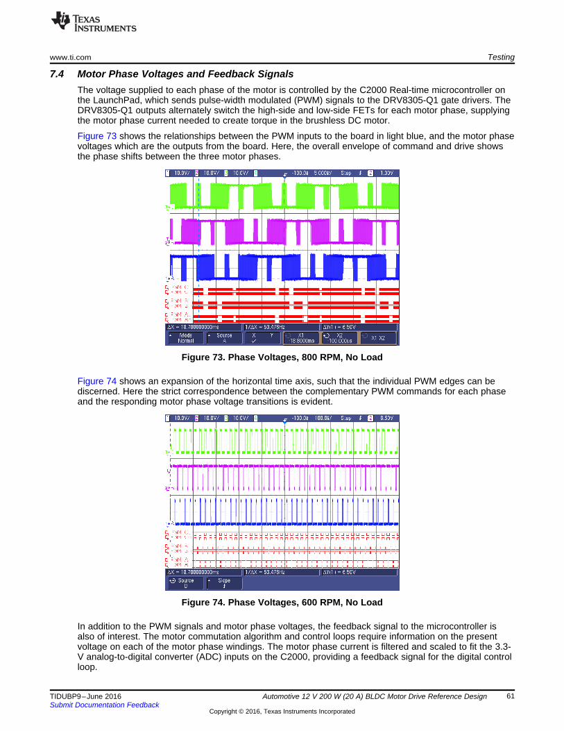
www.ti.com Testing
61TIDUBP9–June 2016Submit Documentation Feedback
Copyright © 2016, Texas Instruments Incorporated
Automotive 12 V 200 W (20 A) BLDC Motor Drive Reference Design
7.4 Motor Phase Voltages and Feedback SignalsThe voltage supplied to each phase of the motor is controlled by the C2000 Real-time microcontroller onthe LaunchPad, which sends pulse-width modulated (PWM) signals to the DRV8305-Q1 gate drivers. TheDRV8305-Q1 outputs alternately switch the high-side and low-side FETs for each motor phase, supplyingthe motor phase current needed to create torque in the brushless DC motor.
Figure 73 shows the relationships between the PWM inputs to the board in light blue, and the motor phasevoltages which are the outputs from the board. Here, the overall envelope of command and drive showsthe phase shifts between the three motor phases.
Figure 73. Phase Voltages, 800 RPM, No Load
Figure 74 shows an expansion of the horizontal time axis, such that the individual PWM edges can bediscerned. Here the strict correspondence between the complementary PWM commands for each phaseand the responding motor phase voltage transitions is evident.
Figure 74. Phase Voltages, 600 RPM, No Load
In addition to the PWM signals and motor phase voltages, the feedback signal to the microcontroller isalso of interest. The motor commutation algorithm and control loops require information on the presentvoltage on each of the motor phase windings. The motor phase current is filtered and scaled to fit the 3.3-V analog-to-digital converter (ADC) inputs on the C2000, providing a feedback signal for the digital controlloop.

Testing www.ti.com
62 TIDUBP9–June 2016Submit Documentation Feedback
Copyright © 2016, Texas Instruments Incorporated
Automotive 12 V 200 W (20 A) BLDC Motor Drive Reference Design
7.5 Dead-Time Settings and PWM SignalsThe pulse-width modulation signals to the drive FETs must incorporate sufficient dead-time such that thehigh-side FETs and low-side FETs for any motor phase are never on at the same time. This causes ashort-circuit between the 12-V supply and ground through the high-side and low-side FETs, resulting inhigh shoot through current.
The algorithms in the MotorWare code include provisions for setting a variable dead-time between theedges of the PWM signals from the LaunchPad to the TIDA-00901 board. The DRV8305-Q1 also hasintegrated logic to prevent current shoot through. TI recommends using the logic in the DRV8305-Q1 tocontrol the dead-time, as this logic monitors the states of the FETs directly.
The dead-time on the rising and falling edges of the PWM signal from the C2000 on the LaunchPad canbe independently set, by altering the code in the hardware abstraction layer file, hal.h, as shown inFigure 75.
NOTE: The unit of time is system clock periods, which for the TMS320F28027F LaunchPad is 16.7nanoseconds (the reciprocal of the 60 MHz system clock frequency). Integer multiples of theclock period are valid settings for these parameters.
Figure 75. Code Fragment in hal.h, Allowing Setting the PWM Dead-Time Parameters
Due to the integrated features of the DRV8305N-Q1 such as programmable dead time control and shoot-through protection, the dead-time setting for the microcontroller can be reduced below the default value of4 system clock cycles (67 nanoseconds). Figure 76 and Figure 77 show the two PWM signals associatedwith motor phase A, and illustrate the adjustability of the dead-time parameter, in this case for the fallingedge.
In both plots, the measured dead-time between transitions is as expected.
Figure 76. PWM Phase A HI (Blue) and Low (Magenta) With C2000 Dead-Time = 1
www.ti.com Testing
63TIDUBP9–June 2016Submit Documentation Feedback
Copyright © 2016, Texas Instruments Incorporated
Automotive 12 V 200 W (20 A) BLDC Motor Drive Reference Design
In Figure 76, the C2000 dead-time is set to 1 clock cycle, and the delay between falling edge on onePWM command signal and the rising edge of the complementary signal is approximately 17 ns. In Figure71, the C2000 dead-time is set to 5 clock cycles, and the delay between falling and rising edges hasincreased to about 82 ns.
Figure 77. PWM Phase A HI (Blue) and Low (Magenta) With C2000 Dead-Time = 5
7.6 Effect of Adjusting the DRV8305 ParametersThe DRV8305N-Q1 provides programmability for several key motor drive parameters. Designers canmodify these parameters through the SPI port. This can ease motor drive development by allowingoptimization of the design without the need to remove and replace discrete components for each motorphase.
In several of the following plots, the specific settings for motor drive parameters are noted below thefigures.
7.6.1 Adjusting Dead-Time in DRV8305 RegistersThe dead-time between falling edge of one gate and the rising edge of the complementary gate can beadjusted through the register settings of the DRV8305-Q1. In Figure 78, the adjustability is shown; the leftplot shows a delay of about 780 ns between the falling edge on the low-side gate drive signal and therising edge of the high-side gate drive signal. The right plot shows that after changing the dead-timesetting through the DRV8305-Q1 SPI port, the delay between falling edge and rising edge has beenincreased to about 1.62 μs.
Figure 78. Gate Drive Signals for Motor Phase A Illustrating Programmable Dead-Time

Testing www.ti.com
64 TIDUBP9–June 2016Submit Documentation Feedback
Copyright © 2016, Texas Instruments Incorporated
Automotive 12 V 200 W (20 A) BLDC Motor Drive Reference Design
7.6.2 Adjusting Gate Drive Current Affects Switching DelayThe gate drive current settings determine how quickly the gate capacitance is charged and discharged.This affects the delay between transition commands (from the microcontroller) and the beginning of thetransition at the motor phase. It also affects the slew rate of the FET turn-on or turn-off transition. In thissection the switching delay between the PWM command signal and the beginning of FET state transitionis illustrated.
Figure 73 shows that with a relatively weak gate drive current, the delay between the rising edge ofPWM_BH and the rising edge of the phase B motor voltage is about 670 ns.
Figure 79. DRV8305-Q1 and FET Signals With Weak Gate Drive Current
Table 8. Parameter Settings Corresponding to Figure 79
TDN TDP IN_HS IN_LS IP_HS IP_LS T DEAD T BLANK TVDS2,000 2,000 60 60 50 50 1,000 2 4
By increasing the gate source and sink current to 250 mA, as shown in Figure 80, the delay betweenrising edge of PWM_B and the rising edge of the motor phase B voltage has decreased from 676 ns to320 ns.
Figure 80. DRV8305-Q1 and FET Signals With Strong Gate Current Drive
www.ti.com Testing
65TIDUBP9–June 2016Submit Documentation Feedback
Copyright © 2016, Texas Instruments Incorporated
Automotive 12 V 200 W (20 A) BLDC Motor Drive Reference Design
Table 9. Parameter Settings Corresponding to Figure 80
TDN TDP IN_HS IN_LS IP_HS IP_LS T DEAD T BLANK TVDS2,000 2,000 250 250 250 250 1,000 2 4
7.6.3 Adjusting Gate Drive Current Affects Transition NoiseIn addition to timing, the effect of the gate drive current setting can be seen on the waveform shape of themotor phase voltage.
Figure 81 shows undesirable switching noise on the three motor phases.
NOTE: There are two undesirable effects visible; the overshoot on each phase transition, and thecoupling of transients from one phase to another.
These effects are due to the high gate drive settings (1.25 A sink, 1.0 A source) for the DRV8305.
Figure 81. DRV8305-Q1 Parameter Settings
Table 10. Parameter Settings Corresponding to Figure 81
TDN TDP IN_HS IN_LS IP_HS IP_LS T DEAD T BLANK TVDS2,000 2,000 1,250 1,250 1,000 1,000 40 2 4

Testing www.ti.com
66 TIDUBP9–June 2016Submit Documentation Feedback
Copyright © 2016, Texas Instruments Incorporated
Automotive 12 V 200 W (20 A) BLDC Motor Drive Reference Design
Figure 82 shows that reducing the gate drive to 50 mA has reduced the undesirable effects previouslyseen with the strong gate drive levels. Both the overshoot on each transition and the cross-coupling hasbeen eliminated.
Figure 82. DRV8305-Q1 Parameter Settings
Table 11. Parameter Settings Corresponding to Figure 82
TDN TDP IN_HS IN_LS IP_HS IP_LS T DEAD T BLANK TVDS2,000 2,000 50 50 50 50 40 2 4
7.6.4 Adjusting Gate Drive Current Affects Transition RingingExamining the motor phase voltage transition edge more closely, a very high gate drive current levelshows both overshoot and ringing, as seen in Figure 83. This ringing, with an oscillation frequency ofapproximately 130 MHz, may cause undesired electromagnetic emissions. In this example, the sourcecurrent for both the high side and low side FET gates is set to 1 A, and the sink current for the high-sideand low-side FET gates is set to 1.25 A.
Figure 83. Strong Gate Drive Current Causes Ringing on Drive FET Edges
Table 12 lists the ElectroCraft motor, no load, 12-V supply, 300 RPM.

www.ti.com Testing
67TIDUBP9–June 2016Submit Documentation Feedback
Copyright © 2016, Texas Instruments Incorporated
Automotive 12 V 200 W (20 A) BLDC Motor Drive Reference Design
Table 12. Parameter Settings Corresponding to Figure 83
TDN TDP IN_HS IN_LS IP_HS IP_LS T DEAD T BLANK TVDS2,000 2,000 1,250 1,250 1,000 1,000 60 2 4
In Figure 84, the effect of reducing the gate drive current to the minimum settings is evident. With a sinkcurrent of 20 mA and a source current of 10 mA, the ringing has been eliminated. However, observe thechange of time scale and the greatly increased rise time of the motor voltage. With a high gate current, therise time was less than 10 ns, and with a weak gate current, the rise time is about 800 ns.
Figure 84. Weak Gate Drive Current Gives Slow FET Rise Time, With No Ringing
Table 13 lists the ElectroCraft motor, no load, 12-V supply, 300 RPM.
Table 13. Parameter Settings Corresponding to Figure 84
TDN TDP IN_HS IN_LS IP_HS IP_LS T DEAD T BLANK TVDS2,000 2,000 1,250 1,250 1,000 1,000 60 2 4
The effect of changing the gate drive current setting may also be observed in the frequency domain. InFigure 85, the frequency spectrum of the motor drive signals is shown. The left plot shows the spectrumwith strong gate drive, the right plot shows the spectrum with the gate drive current reduced. The peakamplitude and overall spectrum are both reduced with the weaker gate drive current.
Figure 85. Frequency Domain Plots Show Effect of Gate Drive Current Setting
Testing www.ti.com
68 TIDUBP9–June 2016Submit Documentation Feedback
Copyright © 2016, Texas Instruments Incorporated
Automotive 12 V 200 W (20 A) BLDC Motor Drive Reference Design
Another example of this effect is shown in Figure 86 and Figure 87. Here the time domain oscilloscopeplots illustrate the effect of reducing the gate drive on the motor drive voltage transitions. The rising edgeof the phase C motor voltage changes from a few nanoseconds with the minimum gate drive to about 250nanoseconds with the gate current at the maximum setting.
Figure 86. Time Domain Plots, Gate Current Set to maximum (Left), Gate Current Set to Minimum (Right),EC motor Unloaded at 100 RPM

www.ti.com Testing
69TIDUBP9–June 2016Submit Documentation Feedback
Copyright © 2016, Texas Instruments Incorporated
Automotive 12 V 200 W (20 A) BLDC Motor Drive Reference Design
Figure 87 shows the frequency spectrum corresponding to the two cases above. The left plot shows aspectrum peak at 19.25 MHz with the maximum gate current setting. The right plot shows a significantreduction in this peak when the gate current is set to the minimum value.
In general, each application may be optimized by selecting the best combination of gate current drive,dead-time, and other motor parameters. The programmability of the DRV8305-Q1 facilitates thisoptimization by allowing designers to change the parameters through simple SPI commands.
Figure 87. Frequency Domain Plots, Gate Current Set to Maximum (Left), Gate Current Set to Minimum(Right), EC Motor Unloaded at 100 RPM
Optimization of the gate drive current involves reducing the undesired high-frequency content of thetransitions, without causing loss of efficiency due to excessively slow transition times.
7.7 Hall Effect Signal for Motor CommunicationIf Hall Effect sensors are available in the motor, these can be used to determine phase position forcommutation of the motor without the need for sensorless commutation algorithms. Sensors such as theDRV5013-Q1 will provide signal indicating which phases of the motor should be driven high and low tomaintain the desired direction of travel.
Typical Hall Effect signals during motor rotation are shown in Figure 88, showing the phase relationbetween the 3 sensor signal, as well as the effect of varying the motor speed.
Figure 88. Hall Effect Signals, 100 RPM (Left) and 300 RPM (Right)

FAST™ Estimator
F A S Tlux, ngle, peed, orque
Motor Parameters ID
Vbus
Vα_in
Vβ_in
Iα_in
Iβ_in
Angle
Speed
Flux
Torque
Enable Motor Identification
Enable PowerWarp™
Motor Type
Enable Rs Online Recalibration
EST_run
ROM
~Rs
~Rr
~I rated
~ψrated
~Lsd
~Lsq
~θ
~ω
~τ
~ψ ~Irated
Enable Force Angle Startup
Motor Phase
Currents
Motor Phase
Voltages
Bus Voltage
Copyright © 2016, Texas Instruments Incorporated
~θ
~ψ
~ω
~τ
Testing www.ti.com
70 TIDUBP9–June 2016Submit Documentation Feedback
Copyright © 2016, Texas Instruments Incorporated
Automotive 12 V 200 W (20 A) BLDC Motor Drive Reference Design
7.8 Motor Identification Algorithm TestingOne of the features of InstaSPIN-FOC is the ability to identify the parameters of the BLDC motorautomatically. The InstaSPIN FOC Motor Identification algorithm measures all the required electrical motorparameters of an unloaded motor in under two minutes (typical). The motor identification is based onmeasures of the current and voltage for the motor phases, as shown in Figure 89.
NOTE: These measurements are also the basis for sensorless commutation, as the FAST estimatorcalculates the motor flux, angle, speed, and torque.
Figure 89. Automatic Motor Identification Using InstaSPIN
For the testing below, the nominal conditions of 12-V supply, and motor with no dynamometer brake loadwere used. Table 14 and Table 15 list the results of repeated runs of motor identification, and illustrate therepeatable nature of the identification process.
Table 14. Results of Repeated Motor Identification (EC Motor)
TRIAL WINDING RESISTANCE (Ω) WINDING INDUCTANCE (mH)1 0.08298 0.61182 0.08226 0.61643 0.08317 0.61794 0.08225 0.60455 0.08259 0.61676 0.08311 0.62707 0.08362 0.66798 0.08266 0.6331

www.ti.com Testing
71TIDUBP9–June 2016Submit Documentation Feedback
Copyright © 2016, Texas Instruments Incorporated
Automotive 12 V 200 W (20 A) BLDC Motor Drive Reference Design
Table 15. Results of Repeated Motor Identification (IHN06576 Motor)
TRIAL WINDING RESISTANCE (Ω)WINDING
INDUCTANCE(mH)
FLUX (V/Hz)
1 0.2890801 0.28002292 0.2887801 0.2821203 0.12917583 0.2871601 0.2943898 0.12929394 0.2865 0.25135 0.2872 0.28736 0.2843 0.2859 0.12896
7.9 Temperature SensorInclusion of a temperature sensor near the drive FETs allows monitoring of the anticipated highest-temperature section of the board. Table 7 shows the relation between motor drive power during operationand temperature sensor readings from the LMT86-Q1. In Section 7.11, infrared camera images of theboard during these various levels of motor power show the distribution of temperature across the board.
Table 16. Temperature Readings During Board Operation
BRAKELOAD (%) SUPPLY POWER (W) LOAD POWER (W) TEMP SIGNAL (V) TEMPERATURE
0 6.9 1.9 1.660 4010 13.9 7.9 1.658 4115 21 15.4 1.646 4220 34 26.8 1.617 4525 58 46 1.540 5230 91 68 1.34 70
In Table 17 and Figure 90 the temperature readings from the LMT86-Q1 show how the board heats up asthe motor drive is operating for a length of time.
Table 17. Temperature Readings vs Time
ELAPSED TIME(MINUTES)
TEMPSIGNAL VOLTAGE TEMPERATURE (ºC)
1 1.73 343 1.71 365 1.69 388 1.67 3910 1.66 4015 1.64 4221 1.62 4422 1.61 45

Elapsed Time (minutes)
TE
MP
Sig
nal V
olta
ge (
V)
Tem
pera
ture
(°C
)
0 2.5 5 7.5 10 12.5 15 17.5 20 22.5 251.6 0
1.61 4
1.62 8
1.63 12
1.64 16
1.65 20
1.66 24
1.67 28
1.68 32
1.69 36
1.7 40
1.71 44
1.72 48
1.73 52
1.74 56
D008
Testing www.ti.com
72 TIDUBP9–June 2016Submit Documentation Feedback
Copyright © 2016, Texas Instruments Incorporated
Automotive 12 V 200 W (20 A) BLDC Motor Drive Reference Design
Figure 90. Temperature Readings vs Time
7.10 Thermal ShutdownIn order to illustrate the over-temperature fault feature of the DRV8305, the board was subjected to a high-temperature source causing a quick increase in temperature. Figure 91 shows the TEMP signal from theLMT86-Q1 (U2) decreasing in voltage as the board temperature rises. The nFAULT signal goes low whenthe temperature reaches the limit.
Figure 91. Over-Temperature Fault Caused by Externally-Applied Heat Source
www.ti.com Testing
73TIDUBP9–June 2016Submit Documentation Feedback
Copyright © 2016, Texas Instruments Incorporated
Automotive 12 V 200 W (20 A) BLDC Motor Drive Reference Design
7.11 Thermal ImagesIn Figure 92 and Figure 93, the surface temperature of the various components is visible. Each of theimages represents a different level of total system power, set by varying the motor speed and brake loadof the dynamometer attached to the motor. Note that due to the auto-ranging feature of the Fluke Ti-110thermal imaging camera, the various colors in each image represent varying temperature levels. Thebackground (ambient) temperature in each case was room temperature.
Figure 92 shows the temperature profile of the board with the LaunchPad processor running, about 2Watts dissipated in the dynamometer, and about 7 Watts of total system power. Note that the hottest partof the image is the C2000 LaunchPad board; the motor drive stages are not dissipating any significantamount of power.
Figure 92. Thermal Image – No Dynamometer Brake

Testing www.ti.com
74 TIDUBP9–June 2016Submit Documentation Feedback
Copyright © 2016, Texas Instruments Incorporated
Automotive 12 V 200 W (20 A) BLDC Motor Drive Reference Design
In Figure 93, the dynamometer brake load is engaged at 10%, dissipating about 8 Watts in thedynamometer; with total system power about 14 Watts. The DRV8305-Q1 has increased in temperature,while the microcontroller is about the same temperature, and is still the hottest component in the image.The maximum temperature in the image has increased slightly to 46.5 degrees Centigrade.
Figure 93. Thermal Image – 10% Brake

www.ti.com Testing
75TIDUBP9–June 2016Submit Documentation Feedback
Copyright © 2016, Texas Instruments Incorporated
Automotive 12 V 200 W (20 A) BLDC Motor Drive Reference Design
In Figure 94, the dynamometer brake load has been increased to 15%. This gives a mechanical powerdelivered of 15 W, and the electrical power from the 12-V supply is 21 W. Under these conditions, thedrive components such as FETs and sense resistors are beginning to rise significantly in temperature.
Figure 94. Thermal Image – 15% Brake

Testing www.ti.com
76 TIDUBP9–June 2016Submit Documentation Feedback
Copyright © 2016, Texas Instruments Incorporated
Automotive 12 V 200 W (20 A) BLDC Motor Drive Reference Design
In Figure 95 the dynamometer brake load has been increased to 20%. This gives a mechanical powerdelivered of 27 W, and the electrical power from the 12-V supply is 34 W. Although the highesttemperature has risen to 54.3 degrees, the DRV8305N-Q1 (U3) still appears to be the hottest componenton the board.
Figure 95. Thermal Image – 20% Brake
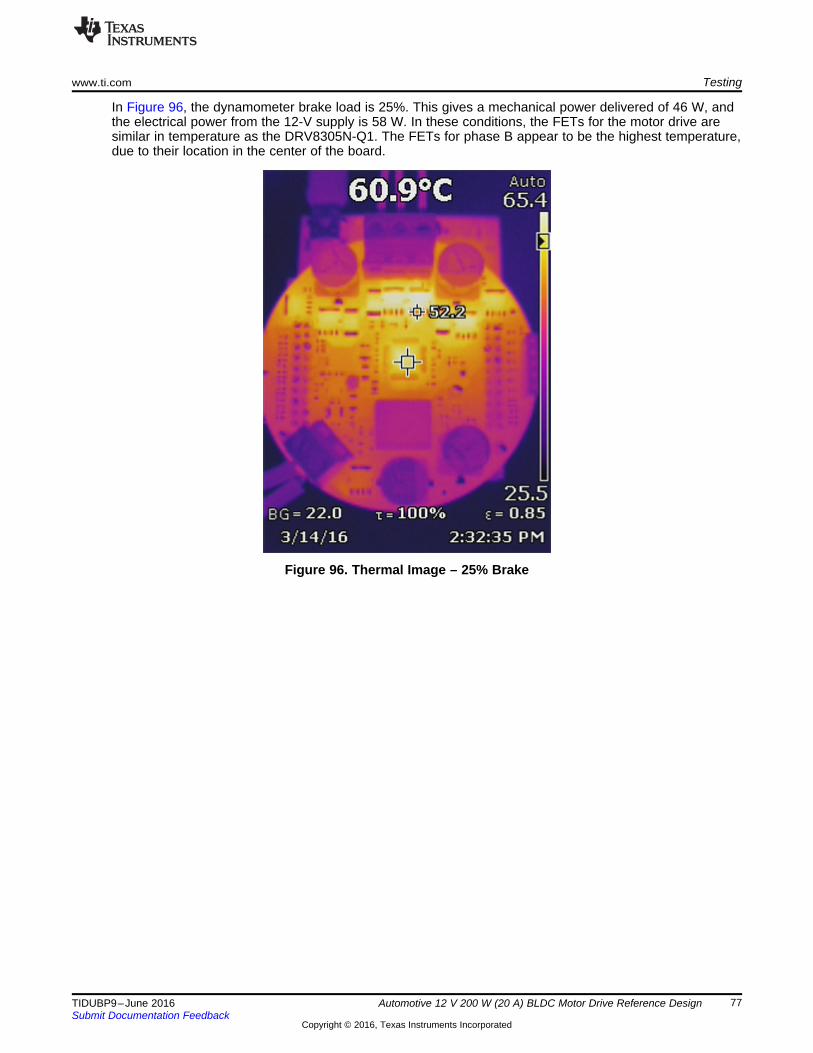
www.ti.com Testing
77TIDUBP9–June 2016Submit Documentation Feedback
Copyright © 2016, Texas Instruments Incorporated
Automotive 12 V 200 W (20 A) BLDC Motor Drive Reference Design
In Figure 96, the dynamometer brake load is 25%. This gives a mechanical power delivered of 46 W, andthe electrical power from the 12-V supply is 58 W. In these conditions, the FETs for the motor drive aresimilar in temperature as the DRV8305N-Q1. The FETs for phase B appear to be the highest temperature,due to their location in the center of the board.
Figure 96. Thermal Image – 25% Brake

Design Files www.ti.com
78 TIDUBP9–June 2016Submit Documentation Feedback
Copyright © 2016, Texas Instruments Incorporated
Automotive 12 V 200 W (20 A) BLDC Motor Drive Reference Design
In Figure 97 the dynamometer brake is set to 30%, causing a power dissipation of 68 Watts in thedynamometer, and a total power from the 12-V supply of 91 Watts. The IR image shows that the top of thehigh-sde FET for phase B is at about 77 degrees, about 50 degrees above room temperature.
Figure 97. Thermal Image – 30% Brake
8 Design FilesTo download the latest version of th electrical schematics for this board, see the design files athttp://www.ti.com/tool/TIDA-00901.
8.1 Bill of MaterialsTo download the bill of materials (BOM), see the design files at TIDA-00901.
Table 18. BOM
ITEM DESIGNATOR QTY PART NUMBER DESCRIPTION1 !PCB1 1 TIDA-00901 Printed Circuit Board
2 C1, C2, C3 3 UMK107AB7105KA-T CAP, CERM, 1 µF, 50 V,±10%, X7R, 0603
3 C4, C5 2 GRM21BR71H105KA12L CAP, CERM, 1uF, 50 V,±10%, X7R, 0805
4 C6, C7, C14, C32, C37 5 C1608X7R1H104K CAP, CERM, 0.1uF, 50 V,±10%, X7R, 0603
5 C8, C9, C12, C13 4 EEE-FT1H331AP CAP, AL, 330 µF, 50 V,±20%, 0.3 Ω, SMD
6 C10, C11 2 C1608X7R1H103K CAP, CERM, 0.01 uF, 50 V,±10%, X7R, 0603
7 C15 – C18 4 C0603C104J4RACTU CAP, CERM, 0.1 µF, 16 V,±5%, X7R, 0603
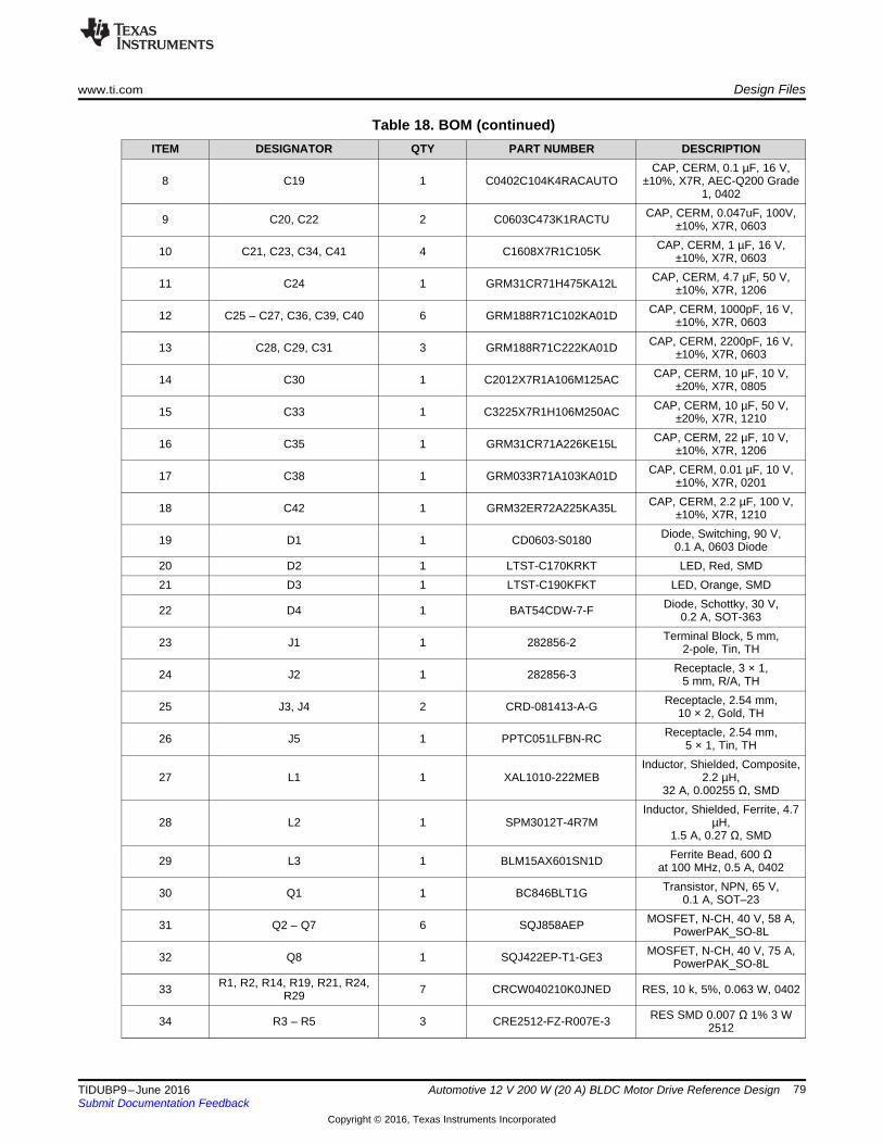
www.ti.com Design Files
79TIDUBP9–June 2016Submit Documentation Feedback
Copyright © 2016, Texas Instruments Incorporated
Automotive 12 V 200 W (20 A) BLDC Motor Drive Reference Design
Table 18. BOM (continued)ITEM DESIGNATOR QTY PART NUMBER DESCRIPTION
8 C19 1 C0402C104K4RACAUTOCAP, CERM, 0.1 µF, 16 V,
±10%, X7R, AEC-Q200 Grade1, 0402
9 C20, C22 2 C0603C473K1RACTU CAP, CERM, 0.047uF, 100V,±10%, X7R, 0603
10 C21, C23, C34, C41 4 C1608X7R1C105K CAP, CERM, 1 µF, 16 V,±10%, X7R, 0603
11 C24 1 GRM31CR71H475KA12L CAP, CERM, 4.7 µF, 50 V,±10%, X7R, 1206
12 C25 – C27, C36, C39, C40 6 GRM188R71C102KA01D CAP, CERM, 1000pF, 16 V,±10%, X7R, 0603
13 C28, C29, C31 3 GRM188R71C222KA01D CAP, CERM, 2200pF, 16 V,±10%, X7R, 0603
14 C30 1 C2012X7R1A106M125AC CAP, CERM, 10 µF, 10 V,±20%, X7R, 0805
15 C33 1 C3225X7R1H106M250AC CAP, CERM, 10 µF, 50 V,±20%, X7R, 1210
16 C35 1 GRM31CR71A226KE15L CAP, CERM, 22 µF, 10 V,±10%, X7R, 1206
17 C38 1 GRM033R71A103KA01D CAP, CERM, 0.01 µF, 10 V,±10%, X7R, 0201
18 C42 1 GRM32ER72A225KA35L CAP, CERM, 2.2 µF, 100 V,±10%, X7R, 1210
19 D1 1 CD0603-S0180 Diode, Switching, 90 V,0.1 A, 0603 Diode
20 D2 1 LTST-C170KRKT LED, Red, SMD21 D3 1 LTST-C190KFKT LED, Orange, SMD
22 D4 1 BAT54CDW-7-F Diode, Schottky, 30 V,0.2 A, SOT-363
23 J1 1 282856-2 Terminal Block, 5 mm,2-pole, Tin, TH
24 J2 1 282856-3 Receptacle, 3 × 1,5 mm, R/A, TH
25 J3, J4 2 CRD-081413-A-G Receptacle, 2.54 mm,10 × 2, Gold, TH
26 J5 1 PPTC051LFBN-RC Receptacle, 2.54 mm,5 × 1, Tin, TH
27 L1 1 XAL1010-222MEBInductor, Shielded, Composite,
2.2 µH,32 A, 0.00255 Ω, SMD
28 L2 1 SPM3012T-4R7MInductor, Shielded, Ferrite, 4.7
µH,1.5 A, 0.27 Ω, SMD
29 L3 1 BLM15AX601SN1D Ferrite Bead, 600 Ωat 100 MHz, 0.5 A, 0402
30 Q1 1 BC846BLT1G Transistor, NPN, 65 V,0.1 A, SOT–23
31 Q2 – Q7 6 SQJ858AEP MOSFET, N-CH, 40 V, 58 A,PowerPAK_SO-8L
32 Q8 1 SQJ422EP-T1-GE3 MOSFET, N-CH, 40 V, 75 A,PowerPAK_SO-8L
33 R1, R2, R14, R19, R21, R24,R29 7 CRCW040210K0JNED RES, 10 k, 5%, 0.063 W, 0402
34 R3 – R5 3 CRE2512-FZ-R007E-3 RES SMD 0.007 Ω 1% 3 W2512
Design Files www.ti.com
80 TIDUBP9–June 2016Submit Documentation Feedback
Copyright © 2016, Texas Instruments Incorporated
Automotive 12 V 200 W (20 A) BLDC Motor Drive Reference Design
Table 18. BOM (continued)ITEM DESIGNATOR QTY PART NUMBER DESCRIPTION
35 R6 – R9 4 CRCW040225K5FKED RES, 25.5 k, 1%, 0.063 W,0402
36 R10 – R13 4 CRCW04024K99FKED RES, 4.99 k, 1%, 0.063 W,0402
37 R15 1 ERJ-2GE0R00X RES, 0, 5%, 0.063 W, 0402
38 R16 – R18 3 CRCW04021K00JNED RES, 1.0 k, 5%, 0.063 W,0402
39 R20 1 CRCW0402100RFKED RES, 100, 1%, 0.063 W, 040240 R22, R23, R25 3 CRCW040256R0JNED RES, 56, 5%, 0.063 W, 040241 R26, R27, R28 3 CRCW040215K0JNED RES, 15 k, 5%, 0.063 W, 040242 R30, R31 2 CRCW0402330RJNED RES, 330, 5%, 0.063 W, 0402
43 TP1, TP3 2 5006 Test Point, Compact, Black,TH
44 TP2 1 5005 Test Point, Compact, Red, TH
45 U2 1 LMT86QDCKRQ1SC70 Analog Temperature
Sensor with Class-AB Output,DCK0005A
46 U3 1 DRV8305NPHPQ1
Three Phase Automotive GateDriver with Three IntegratedCurrent Shunt Amplifiers and
Voltage Regulator, PHP0048G
47 U4 1 LM53600NQDSXRQ1 Synchronous Buck Regulatorfor 650 mA, DSX0010A
48 FID1, FID2, FID3 0 N/A Fiducial mark. There is nothingto buy or mount.
8.2 PCB Layout Recommendations
8.2.1 General Notes on Noise Sensitive Traces and Components• Route voltage feedback traces away from other noisy traces or components, such as clock lines. Avoid
routing things under the switch node of a power inductor altogether if possible• Feedback nodes are generally high impedance lines which are quite sensitive to disturbances. The
switch node can radiate a significant amount of energy and could couple noise into FB traces or othersensitive lines. Placing these traces on the other side of the board (with ground planes between them)helps mitigate ill effects as well.
• Analog and control loop components must be placed such that their trace lengths back to the IC areminimized.
The feedback and compensation nodes are especially high impedance and thus susceptible to picking up.As these are critical in the operation of the devices control loop, poor placement and routing of thesecomponents and traces may effect the performance of the device by introducing unwanted parasiticinductances and capacitances.
8.2.2 PCB Layering RecommendationsThis design uses a 4-layer board, with an internal ground plane to shield the bottom signal layer from theswitch nodes found on the top layer. Figure 98 shows the layer stack-up used in this board.
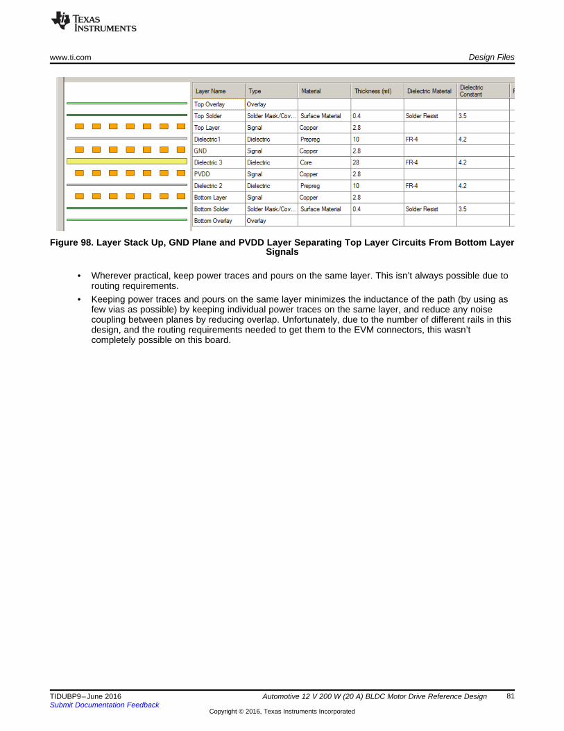
www.ti.com Design Files
81TIDUBP9–June 2016Submit Documentation Feedback
Copyright © 2016, Texas Instruments Incorporated
Automotive 12 V 200 W (20 A) BLDC Motor Drive Reference Design
Figure 98. Layer Stack Up, GND Plane and PVDD Layer Separating Top Layer Circuits From Bottom LayerSignals
• Wherever practical, keep power traces and pours on the same layer. This isn’t always possible due torouting requirements.
• Keeping power traces and pours on the same layer minimizes the inductance of the path (by using asfew vias as possible) by keeping individual power traces on the same layer, and reduce any noisecoupling between planes by reducing overlap. Unfortunately, due to the number of different rails in thisdesign, and the routing requirements needed to get them to the EVM connectors, this wasn’tcompletely possible on this board.

Design Files www.ti.com
82 TIDUBP9–June 2016Submit Documentation Feedback
Copyright © 2016, Texas Instruments Incorporated
Automotive 12 V 200 W (20 A) BLDC Motor Drive Reference Design
8.2.3 General Power Supply Considerations• Input capacitors should be placed as close to the IC as possible to reduce the parasitic series
inductance from the capacitor to the device it is supplying. This is especially important for DCDCconverters as the inductance from the capacitor to the high-side switching FET can cause high voltagespikes and ringing on the switch node, which can be damaging to components and cause problems forEMI.
• Place the input capacitors in order of descending size/value, with the smallest being closest to thedevice input pin. Contrastingly, place the output capacitors in order of descending size/value, with thelargest being closest to the device’s output pins/power inductor.
• Use wide copper areas/traces for routing outputs of the converters to the connectors or loads. Thisreduces the I*R drop along the power path and thus improves load regulation.
• The resistivity of a trace drops as the width of the trace increases (R ∝1/W). If not using DCDC/linearconverters capable of differential remote sensing, care must be taken that the voltage drop from thelocation of regulation (close to the converter) to the load is not significant. While there isn’t really amaximum limit on this, there is a minimum. PCB traces, like wires, are rated for current ranges basedon their cross-sectional area. This depends not only on the width but also on the thickness/height ofthe trace. Calculators are available online for calculating minimum trace width.
• Minimize the loop area and series path inductance of the switching return current in a DCDC converter.It is preferable that this be on the same layer and can be achieved by careful placement of thecomponents.
• Since it is not always convenient to guarantee a good return path on the same layer, we can dropground vias to an internal plane which is not broken up providing a more direct return path. The figurebelow shows the use of these ground vias where it was not possible to create a small loop on the toplayer.
• The power inductors should be close to the switch node pins of the ICs, minimizing the distance fromthe pin to the inductor, but maintaining large area as much as possible. The goal is to minimize boththe parasitic inductance, as well as reduce the radiated emissions from the node:– If a bootstrap capacitor is used, place this component as close to the power inductor as practical.
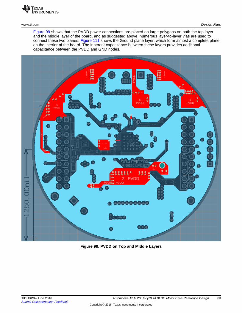
www.ti.com Design Files
83TIDUBP9–June 2016Submit Documentation Feedback
Copyright © 2016, Texas Instruments Incorporated
Automotive 12 V 200 W (20 A) BLDC Motor Drive Reference Design
Figure 99 shows that the PVDD power connections are placed on large polygons on both the top layerand the middle layer of the board, and as suggested above, numerous layer-to-layer vias are used toconnect these two planes. Figure 111 shows the Ground plane layer, which form almost a complete planeon the interior of the board. The inherent capacitance between these layers provides additionalcapacitance between the PVDD and GND nodes.
Figure 99. PVDD on Top and Middle Layers
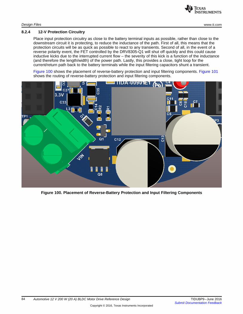
Design Files www.ti.com
84 TIDUBP9–June 2016Submit Documentation Feedback
Copyright © 2016, Texas Instruments Incorporated
Automotive 12 V 200 W (20 A) BLDC Motor Drive Reference Design
8.2.4 12-V Protection CircuitryPlace input protection circuitry as close to the battery terminal inputs as possible, rather than close to thedownstream circuit it is protecting, to reduce the inductance of the path. First of all, this means that theprotection circuits will be as quick as possible to react to any transients. Second of all, in the event of areverse polarity event, the FET controlled by the DRV8305-Q1 will shut off quickly and this could causeinductive kicks due to the interrupted current flow – the severity of this kick is a function of the inductance(and therefore the length/width) of the power path. Lastly, this provides a close, tight loop for thecurrent/return path back to the battery terminals while the input filtering capacitors shunt a transient.
Figure 100 shows the placement of reverse-battery protection and input filtering components. Figure 101shows the routing of reverse-battery protection and input filtering components.
Figure 100. Placement of Reverse-Battery Protection and Input Filtering Components

www.ti.com Design Files
85TIDUBP9–June 2016Submit Documentation Feedback
Copyright © 2016, Texas Instruments Incorporated
Automotive 12 V 200 W (20 A) BLDC Motor Drive Reference Design
Figure 101. Routing of Reverse-Battery Protection and Input Filtering Components

Design Files www.ti.com
86 TIDUBP9–June 2016Submit Documentation Feedback
Copyright © 2016, Texas Instruments Incorporated
Automotive 12 V 200 W (20 A) BLDC Motor Drive Reference Design
8.2.5 3.3-V Buck RegulatorThe following list of layout considerations is in order of importance:1. Place high frequency input bypass capacitor, (C37), as close to the LM53600-Q1 as possible.2. Connect AGND and GND to the DAP immediately adjacent to the LM53600-Q1.3. Do not interrupt the ground plain under the loop containing the LM53600-Q1’s VIN and GND pins and
C37.4. The boot capacitor, C32, should be close to the LM53600-Q1 and the loop from the SW pin, through
the boot capacitor and into the BOOT pin should be kept as small as possible.5. Keep the SW node as small as possible. It should be wide enough to carry the converter’s full current
without significant drop.6. C33 with at least 4.7 µF of bypassing should be close to the LM53600-Q1’s input.7. Place C34, the VCC pin’s bypass, and C38, the bypass for FB for fixed voltage devices and BIAS for
adjustable devices as close to the LM53600-Q1 as possible.8. The first output the trace from the output inductor to the output node should run by an output capacitor
before joining the rest of the output node.9. Keep C35 with at least 10µF close to the LM53600-Q1’s output (output inductor and GND).10. Clear the layer beneath the SW node.
Figure 102 and Figure 103 show the placement and routing for the 3.3-V buck regulator.
Figure 102. Placement for the 3.3-V Buck Regulator
Figure 103. Routing for the 3.3-V Buck Regulator

www.ti.com Design Files
87TIDUBP9–June 2016Submit Documentation Feedback
Copyright © 2016, Texas Instruments Incorporated
Automotive 12 V 200 W (20 A) BLDC Motor Drive Reference Design
8.2.6 Motor Gate DriverThe following layout recommendations were followed when designing the PCB for the DRV8305:• The DVDD bypass capacitor (C23) and AVDD 1-μF bypass capacitor (C21) must connect directly to
the adjacent GND pin to minimize loop impedance for the bypass capacitor.• The CP1 and CP2 0.047-μF flying capacitors (C20 and C22) must be placed directly next to the
DRV8305 charge pump pins.• The VCPH 2.2-μF and VCP_LSD 1-μF bypass capacitors (C41 and C42) should be placed close to
their corresponding pins with a direct path back to the DRV8305-Q1 GND net.• The PVDD 4.7-μF bypass capacitor (C24) should be placed as close as possible to the DRV8305
PVDD supply pin.• Use the proper footprint as shown in the Mechanical, Packaging, and Orderable Information section.• Minimize the loop length for the high-side and low-side gate drivers. The high-side loop is from the
DRV8305 GH_X to the power MOSFET and returns through SH_X. The low-side loop is from theDRV8305 GL_X to the power MOSFET and returns through SL_X.
Figure 104 and Figure 105 show the placement and routing for 3-Phase automotive gate driver.
Figure 104. Placement for 3-Phase Automotive Gate Driver Figure 105. Routing for 3-Phase Automotive Gate Driver

Design Files www.ti.com
88 TIDUBP9–June 2016Submit Documentation Feedback
Copyright © 2016, Texas Instruments Incorporated
Automotive 12 V 200 W (20 A) BLDC Motor Drive Reference Design
8.2.7 Motor Drive CircuitThe components related to the drive stage for each phase of the motor are grouped together, and thelayout of each of the phases is similar. The power FETs and associated components are located on thetop side of the board, as is the DRV8305-Q1 gate driver (U3). The two power FETs for each motor phaseare located in close proximity, and such that the shared output node MOT_A, MOT_B, or MOT_Cconnects them with solid current path. The current sense resistor (R3, R4, R5) for each phase is alsolocated as close as possible to the motor phase traces.
C8 and C9 (330 uF) and C1, C2, and C3 (1 uF) provide a low-inductance reservoir of charge near thehigh-side FETs. They should be located in close proximity to the drive stages to reduce any resistance orinductance between the stored charge and the drive FETs.
Figure 106 shows the layout of the motor drive stages.
Figure 106. Layout of Motor Drive Stages
8.2.8 Differential SignalsIn the case of differential signals, such as the motor current feedback across the current sense resistors,use symmetry to ensure that any noise picked up on one line is also picked up approximately equally onthe other line.
Figure 107 shows the layout symmetry used to reduce differential-mode noise on analog signal.
Figure 107. Layout Symmetry Used to Reduce Differential-Mode Noise on Analog Signal
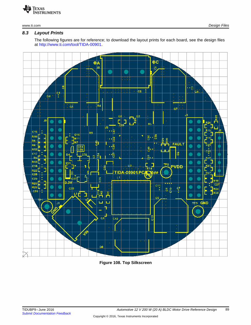
www.ti.com Design Files
89TIDUBP9–June 2016Submit Documentation Feedback
Copyright © 2016, Texas Instruments Incorporated
Automotive 12 V 200 W (20 A) BLDC Motor Drive Reference Design
8.3 Layout PrintsThe following figures are for reference; to download the layout prints for each board, see the design filesat http://www.ti.com/tool/TIDA-00901.
Figure 108. Top Silkscreen

Design Files www.ti.com
90 TIDUBP9–June 2016Submit Documentation Feedback
Copyright © 2016, Texas Instruments Incorporated
Automotive 12 V 200 W (20 A) BLDC Motor Drive Reference Design
Figure 109. Top Solder Mask
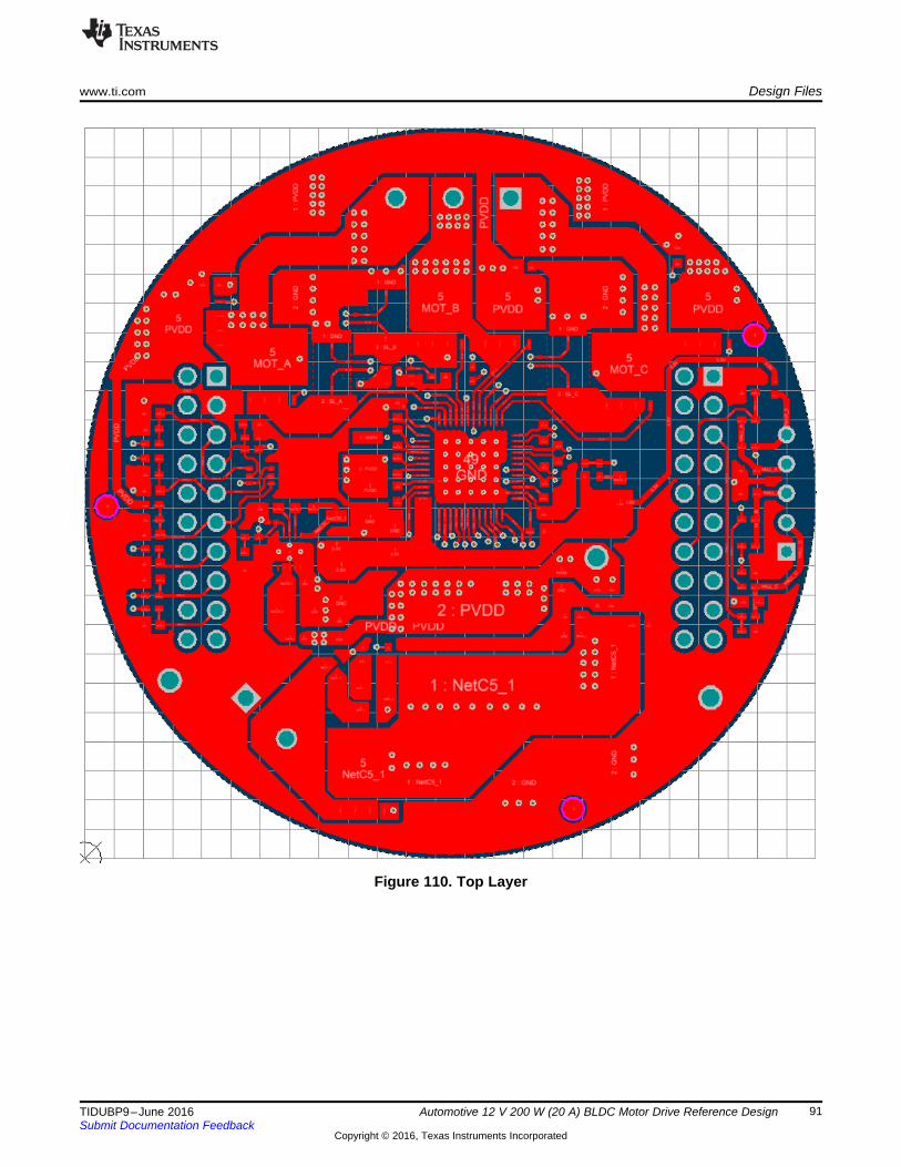
www.ti.com Design Files
91TIDUBP9–June 2016Submit Documentation Feedback
Copyright © 2016, Texas Instruments Incorporated
Automotive 12 V 200 W (20 A) BLDC Motor Drive Reference Design
Figure 110. Top Layer
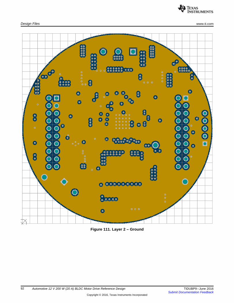
Design Files www.ti.com
92 TIDUBP9–June 2016Submit Documentation Feedback
Copyright © 2016, Texas Instruments Incorporated
Automotive 12 V 200 W (20 A) BLDC Motor Drive Reference Design
Figure 111. Layer 2 – Ground

www.ti.com Design Files
93TIDUBP9–June 2016Submit Documentation Feedback
Copyright © 2016, Texas Instruments Incorporated
Automotive 12 V 200 W (20 A) BLDC Motor Drive Reference Design
Figure 112. Layer 3 – Power

Design Files www.ti.com
94 TIDUBP9–June 2016Submit Documentation Feedback
Copyright © 2016, Texas Instruments Incorporated
Automotive 12 V 200 W (20 A) BLDC Motor Drive Reference Design
Figure 113. Bottom Layer

www.ti.com Design Files
95TIDUBP9–June 2016Submit Documentation Feedback
Copyright © 2016, Texas Instruments Incorporated
Automotive 12 V 200 W (20 A) BLDC Motor Drive Reference Design
Figure 114. Bottom Solder

Design Files www.ti.com
96 TIDUBP9–June 2016Submit Documentation Feedback
Copyright © 2016, Texas Instruments Incorporated
Automotive 12 V 200 W (20 A) BLDC Motor Drive Reference Design
Figure 115. Bottom Silkscreen (Flipped)

www.ti.com Design Files
97TIDUBP9–June 2016Submit Documentation Feedback
Copyright © 2016, Texas Instruments Incorporated
Automotive 12 V 200 W (20 A) BLDC Motor Drive Reference Design
Figure 116. Mechanical Dimensions
8.4 Altium Project and Gerber FilesTo download the Altium project and Gerber files for each board, see the design files at TIDA-00901.
Software Files www.ti.com
98 TIDUBP9–June 2016Submit Documentation Feedback
Copyright © 2016, Texas Instruments Incorporated
Automotive 12 V 200 W (20 A) BLDC Motor Drive Reference Design
9 Software FilesTo download the Code Composer Studio Integrates Development Environment, seehttp://www.ti.com/tool/CCSTUDIO.
To download the MotorWare Software packages, see http://www.ti.com/tool/MOTORWARE.
10 References
1. DRV8305-Q1 Three-Phase Automotive Smart Gate Driver With Three Integrated Current ShuntAmplifiers and Voltage Regulator (SLVSD12).
2. LMT86/LMT86-Q1 SC70/TO-92, Analog Temperature Sensors with Class-AB Output (SNIS169).3. LM53600/01-Q1, 0.65A/1A, 36V Synchronous, 2.1MHz, Automotive Step Down DC-DC Converter
(SNAS660).4. DRV5013 -Q1 Automotive Digital-Latch Hall Effect Sensor (SLIS162C).5. TMS320F28026F, TMS320F28027F InstaSPIN-FOC Software Technical Reference Manual
(SPRUHP4).6. Understanding IDRIVE and TDRIVE in TI Motor Gate Drivers (SLVA414).7. Simple Success with Conducted EMI from DC-DC Converters (SNVA489).8. MotorWare Software, http://www.ti.com/MotorWare9. InstaSPIN / MotorWare GUI, http://www.ti.com/tool/instaspinuniversalgui10. Webench Design Center, http://www.ti.com/webench.
11 TerminologyADC: Analog-to-Digital Converter
BOM: Bill of Materials
Buck: Step-down switching-mode voltage converter
CAN:Controller Area Network
CCS: Code Composer Studio
EMC: Electromagnetic Compatibility
EMF: Electromotive Force
FET: Field Effect Transistor
FOC: Field Oriented Control
GND: Ground
IR: Infrared
MOSFET: Metal Oxide Semiconductor Field Effect Transistor
OEM: Original Equipment Manufacturer
PCB: Printed Circuit Board
RC: Resistor Capacitor
RCD: Resistor Capacitor Diode
SPICE: Simulation Program
TIDA: TI Design

www.ti.com About the Author
99TIDUBP9–June 2016Submit Documentation Feedback
Copyright © 2016, Texas Instruments Incorporated
Automotive 12 V 200 W (20 A) BLDC Motor Drive Reference Design
12 About the AuthorCLARK KINNAIRD is a Systems Applications Engineer at Texas Instruments. As a member of theAutomotive Systems Engineering team, Clark works on various types of motor drive end-equipment,creating reference designs for automotive manufacturers. Clark earned his Bachelor of Science andMaster of Science in Engineering from the University of Florida, and his Ph.D. in Electrical Engineeringfrom Southern Methodist University.

www.ti.com
100 TIDUBP9–June 2016Submit Documentation Feedback
Copyright © 2016, Texas Instruments Incorporated
Appendix
Appendix A Appendix
A.1 WEBENCH Simulation ModelsFigure 117 shows the WEBENCH electrical schematic for the LM53600-Q1 3.3-V buck regulator.
Figure 117. WEBENCH Electrical Schematic for the LM53600-Q1 3.3-V Buck Regulator.
A.2 TINA Simulation Modelsshows the TINA simulation schematic for motor current feedback circuit.
Figure 118. TINA Simulation for Motor Current Feedback Circuit
Figure 119 shows the TINA simulation schematic for VBAT input filtering.

www.ti.com TINA Simulation Models
101TIDUBP9–June 2016Submit Documentation Feedback
Copyright © 2016, Texas Instruments Incorporated
Appendix
Figure 119. TINA Simulation Schematic for Motor Voltage Feedback Circuit
Figure 120 shows the TINA simulation schematic for VBAT input filtering.
Figure 120. TINA Simulation Schematic for VBAT Input Filtering
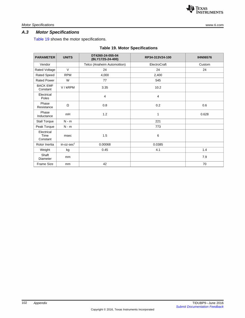
Motor Specifications www.ti.com
102 TIDUBP9–June 2016Submit Documentation Feedback
Copyright © 2016, Texas Instruments Incorporated
Appendix
A.3 Motor SpecificationsTable 19 shows the motor specifications.
Table 19. Motor Specifications
PARAMETER UNITS DT4260-24-055-04(BLY172S-24-400) RP34-313V24-100 IHN06576
Vendor Telco (Anaheim Automottion) ElectroCraft CustomRated Voltage V 24 24 24Rated Speed RPM 4,000 2,400Rated Power W 77 545BACK EMF
Constant V / kRPM 3.35 10.2
ElectricalPoles 4 4
PhaseResistance Ω 0.8 0.2 0.6
PhaseInductance mH 1.2 1 0.628
Stall Torque N - m 221Peak Torque N - m 773
ElectricalTime
Constantmsec 1.5 6
Rotor Inertia in-oz-sec2 0.00068 0.0385Weight kg 0.45 4.1 1.4Shaft
Diameter mm 7.9
Frame Size mm 42 70

IMPORTANT NOTICE FOR TI REFERENCE DESIGNS
Texas Instruments Incorporated (‘TI”) reference designs are solely intended to assist designers (“Designer(s)”) who are developing systemsthat incorporate TI products. TI has not conducted any testing other than that specifically described in the published documentation for aparticular reference design.TI’s provision of reference designs and any other technical, applications or design advice, quality characterization, reliability data or otherinformation or services does not expand or otherwise alter TI’s applicable published warranties or warranty disclaimers for TI products, andno additional obligations or liabilities arise from TI providing such reference designs or other items.TI reserves the right to make corrections, enhancements, improvements and other changes to its reference designs and other items.Designer understands and agrees that Designer remains responsible for using its independent analysis, evaluation and judgment indesigning Designer’s systems and products, and has full and exclusive responsibility to assure the safety of its products and compliance ofits products (and of all TI products used in or for such Designer’s products) with all applicable regulations, laws and other applicablerequirements. Designer represents that, with respect to its applications, it has all the necessary expertise to create and implementsafeguards that (1) anticipate dangerous consequences of failures, (2) monitor failures and their consequences, and (3) lessen thelikelihood of failures that might cause harm and take appropriate actions. Designer agrees that prior to using or distributing any systemsthat include TI products, Designer will thoroughly test such systems and the functionality of such TI products as used in such systems.Designer may not use any TI products in life-critical medical equipment unless authorized officers of the parties have executed a specialcontract specifically governing such use. Life-critical medical equipment is medical equipment where failure of such equipment would causeserious bodily injury or death (e.g., life support, pacemakers, defibrillators, heart pumps, neurostimulators, and implantables). Suchequipment includes, without limitation, all medical devices identified by the U.S. Food and Drug Administration as Class III devices andequivalent classifications outside the U.S.Designers are authorized to use, copy and modify any individual TI reference design only in connection with the development of endproducts that include the TI product(s) identified in that reference design. HOWEVER, NO OTHER LICENSE, EXPRESS OR IMPLIED, BYESTOPPEL OR OTHERWISE TO ANY OTHER TI INTELLECTUAL PROPERTY RIGHT, AND NO LICENSE TO ANY TECHNOLOGY ORINTELLECTUAL PROPERTY RIGHT OF TI OR ANY THIRD PARTY IS GRANTED HEREIN, including but not limited to any patent right,copyright, mask work right, or other intellectual property right relating to any combination, machine, or process in which TI products orservices are used. Information published by TI regarding third-party products or services does not constitute a license to use such productsor services, or a warranty or endorsement thereof. Use of the reference design or other items described above may require a license from athird party under the patents or other intellectual property of the third party, or a license from TI under the patents or other intellectualproperty of TI.TI REFERENCE DESIGNS AND OTHER ITEMS DESCRIBED ABOVE ARE PROVIDED “AS IS” AND WITH ALL FAULTS. TI DISCLAIMSALL OTHER WARRANTIES OR REPRESENTATIONS, EXPRESS OR IMPLIED, REGARDING THE REFERENCE DESIGNS OR USE OFTHE REFERENCE DESIGNS, INCLUDING BUT NOT LIMITED TO ACCURACY OR COMPLETENESS, TITLE, ANY EPIDEMIC FAILUREWARRANTY AND ANY IMPLIED WARRANTIES OF MERCHANTABILITY, FITNESS FOR A PARTICULAR PURPOSE, AND NON-INFRINGEMENT OF ANY THIRD PARTY INTELLECTUAL PROPERTY RIGHTS.TI SHALL NOT BE LIABLE FOR AND SHALL NOT DEFEND OR INDEMNIFY DESIGNERS AGAINST ANY CLAIM, INCLUDING BUT NOTLIMITED TO ANY INFRINGEMENT CLAIM THAT RELATES TO OR IS BASED ON ANY COMBINATION OF PRODUCTS ASDESCRIBED IN A TI REFERENCE DESIGN OR OTHERWISE. IN NO EVENT SHALL TI BE LIABLE FOR ANY ACTUAL, DIRECT,SPECIAL, COLLATERAL, INDIRECT, PUNITIVE, INCIDENTAL, CONSEQUENTIAL OR EXEMPLARY DAMAGES IN CONNECTION WITHOR ARISING OUT OF THE REFERENCE DESIGNS OR USE OF THE REFERENCE DESIGNS, AND REGARDLESS OF WHETHER TIHAS BEEN ADVISED OF THE POSSIBILITY OF SUCH DAMAGES.TI’s standard terms of sale for semiconductor products (http://www.ti.com/sc/docs/stdterms.htm) apply to the sale of packaged integratedcircuit products. Additional terms may apply to the use or sale of other types of TI products and services.Designer will fully indemnify TI and its representatives against any damages, costs, losses, and/or liabilities arising out of Designer’s non-compliance with the terms and provisions of this Notice.IMPORTANT NOTICE
Mailing Address: Texas Instruments, Post Office Box 655303, Dallas, Texas 75265Copyright © 2016, Texas Instruments Incorporated