authors: eng. laura quesada del busto eng. gustavo javier ... · research & development...
TRANSCRIPT

RESEARCH & DEVELOPMENT TELECOMMUNICATION’S INSTITUTE
Authors: Eng. Laura Quesada del BustoEng. Gustavo Javier Aguirre Soler
III TVD International Forum Havana, September 2015

RESEARCH & DEVELOPMENT TELECOMMUNICATION’S INSTITUTE
Decoding
Introduction (1/3)
2/24
Multiplexing Modulation
DemodulationDemultiplexing
Encoding
Decoding
TX
RX
Digital Terrestrial Television System
Encoding

RESEARCH & DEVELOPMENT TELECOMMUNICATION’S INSTITUTE
Introduction (2/3)
3/24
FPGA software/hardware co-design for the H.264/AVC decoder implemented in LACETEL
Embedded system on a Xilinx
Virtex 5 FPGA.
Xilinx ML507 evaluation board
The H.264/AVC decoder software
is run on the PowerPC processor
The communication between the
PowerPC processor and the
hardware is done over PLB bus.

RESEARCH & DEVELOPMENT TELECOMMUNICATION’S INSTITUTE
Introduction (3/3)
4/24
Bypass decoding
Binary arithmetic decoding
engine.
De-binarization
Context
Model
Termination
Bypass
Regular
Video
parameters
CABAC Decoding process
Bypass Decoding IP module implemented in VHDL, in 2014
H.264/AVC
Binary
code

RESEARCH & DEVELOPMENT TELECOMMUNICATION’S INSTITUTE
Problematic Situation
5/24
The FPGA-based H.264/AVC decoder implemented in
LACETEL:
• does not meet time requirements to become a practical
final solution.
• does not have complementary tools to identify and
experiment with blocks that are critical in terms of speed.

RESEARCH & DEVELOPMENT TELECOMMUNICATION’S INSTITUTE
Main Goal
Insert the Bypass Arithmetic Decoding IP module of CABAC
in the H.264/AVC decoder model, and necessary timing tools
to evaluate the system behavior.
6/24

RESEARCH & DEVELOPMENT TELECOMMUNICATION’S INSTITUTE
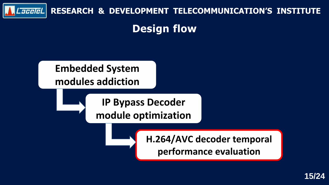
Design flow
7/24
Modules addiction to theEmbedded System
Bypass Decoder IP module optimization
H.264/AVC decoder temporal performance evaluation

RESEARCH & DEVELOPMENT TELECOMMUNICATION’S INSTITUTE
modules addiction to the embedded system (1/3)
8/24
PowerPC 440
UART
COMPACTFLASH
SRAM
INTC
BRAM PLB
Bu
s
Interrupt Controller
• Connected as a 32 bits slave of Bus PLB.
• Two interrupt inputs used.
• Single interrupt output.
• Priority between interrupt requests determined.
• Each input configured for rising edge sensitivity.
Processor Frec = 125 MHz
Bus Frec = 125 MHz

RESEARCH & DEVELOPMENT TELECOMMUNICATION’S INSTITUTE
9/24
Processor Frec = 125 MHz
Bus Frec = 125 MHz
Timer/Counter
• Connected as a 32 bits slave of Bus PLB.
• Configured in Generation Mode.
• Interrupt output signal to the interrupt controller.
PowerPC 440
INTC
UART
COMPACTFLASH
SRAM
TIMER
BRAM PLB
Bu
s
modules addiction to the embedded system (2/3)

RESEARCH & DEVELOPMENT TELECOMMUNICATION’S INSTITUTE
10/24
Processor Frec = 125 MHz
Bus Frec = 125 MHz
Bypass Decoder IP module
Hardware module in charge ofdoing bypass decoding ofCABAC.
PowerPC 440
INTC
Bu
s P
LB
UART
COMPACTFLASH
SRAM
TIMER
BYPASSDECODER
BRAM
modules addiction to the embedded system (3/3)

RESEARCH & DEVELOPMENT TELECOMMUNICATION’S INSTITUTE
Design flow
11/24
Embedded System modules addiction
Bypass Decoder IP module optimization
H.264/AVC decoder temporalperformance evaluation

RESEARCH & DEVELOPMENT TELECOMMUNICATION’S INSTITUTE
Decoder Bypass IP module previous implementation
12/24
Bypassdecoder
Bus PLB
PowerPC
Test Bench
• Implemented in a test system with the PowerPC
processor and the PLB Bus.
• The processor polls the module’s outputs to know when
the values are ready.

RESEARCH & DEVELOPMENT TELECOMMUNICATION’S INSTITUTE
Bypass Decoder IP module optimization (1/3)
13/24
Decoder Bypass IP module previous implementation:
• Twelve software registers
• Single intern signal in each register
Decoder Bypass IP module optimized:
• Six software registers.
• Many intern signals in each register.
• Memory consumption reduced.

RESEARCH & DEVELOPMENT TELECOMMUNICATION’S INSTITUTE
Bypass Decoder IP module optimization (3/3)
14/24
Bypass Decoder IP moduleprocessing time
9,6 ns
> PLB single data beat read time
32 ns
It is possible just to read and write the data from processor to theBypass IP module without using any method like the poll or theinterruption.
RESEARCH & DEVELOPMENT TELECOMMUNICATION’S INSTITUTE
Design flow
15/24
Embedded System modules addiction
IP Bypass Decoder module optimization
H.264/AVC decoder temporalperformance evaluation
RESEARCH & DEVELOPMENT TELECOMMUNICATION’S INSTITUTE
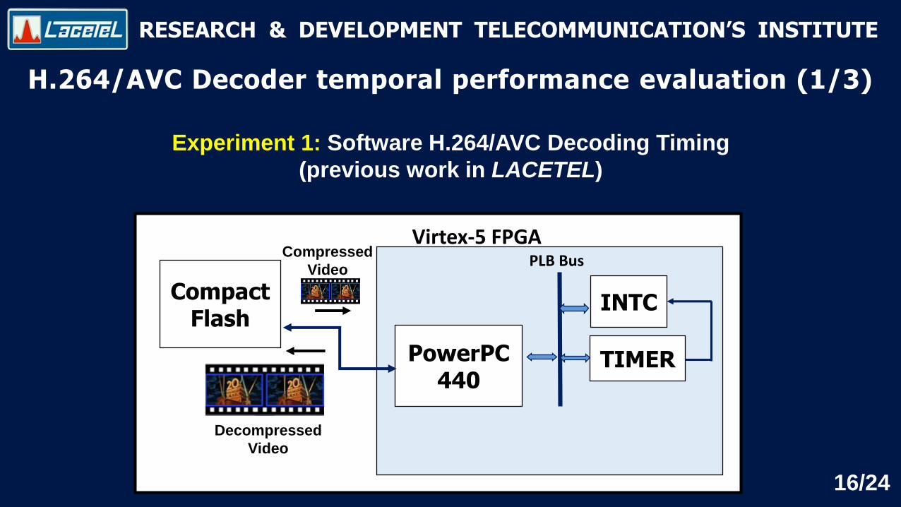
H.264/AVC Decoder temporal performance evaluation (1/3)
16/24
Compact Flash
PowerPC440
TIMER
INTC
Virtex-5 FPGAPLB Bus
Compressed
Video
Decompressed
Video
Experiment 1: Software H.264/AVC Decoding Timing
(previous work in LACETEL)

RESEARCH & DEVELOPMENT TELECOMMUNICATION’S INSTITUTE
H.264/AVC Decoder temporal performance evaluation (2/3)
17/24
Compact Flash
PowerPC440
TIMER
INTC
BYPASSDECODER
Experiment 2: Software/Hardware H.264/AVC Decoding Timing
(with Bypass Decoder IP module on)
Virtex-5 FPGAPLB Bus
Compressed
Video
Decompressed
Video

RESEARCH & DEVELOPMENT TELECOMMUNICATION’S INSTITUTE
H.264/AVC Decoder temporal performance evaluation (3/3)
18/24
Compact Flash
PowerPC440
TIMER
INTC
OptimizedBYPASS
DECODER
Experiment 3: Software/Hardware H.264/AVC Decoding Timing
(with optimized Bypass Decoder IP module on)
Virtex-5 FPGAPLB Bus
Compressed
Video
Decompressed
Video
RESEARCH & DEVELOPMENT TELECOMMUNICATION’S INSTITUTE
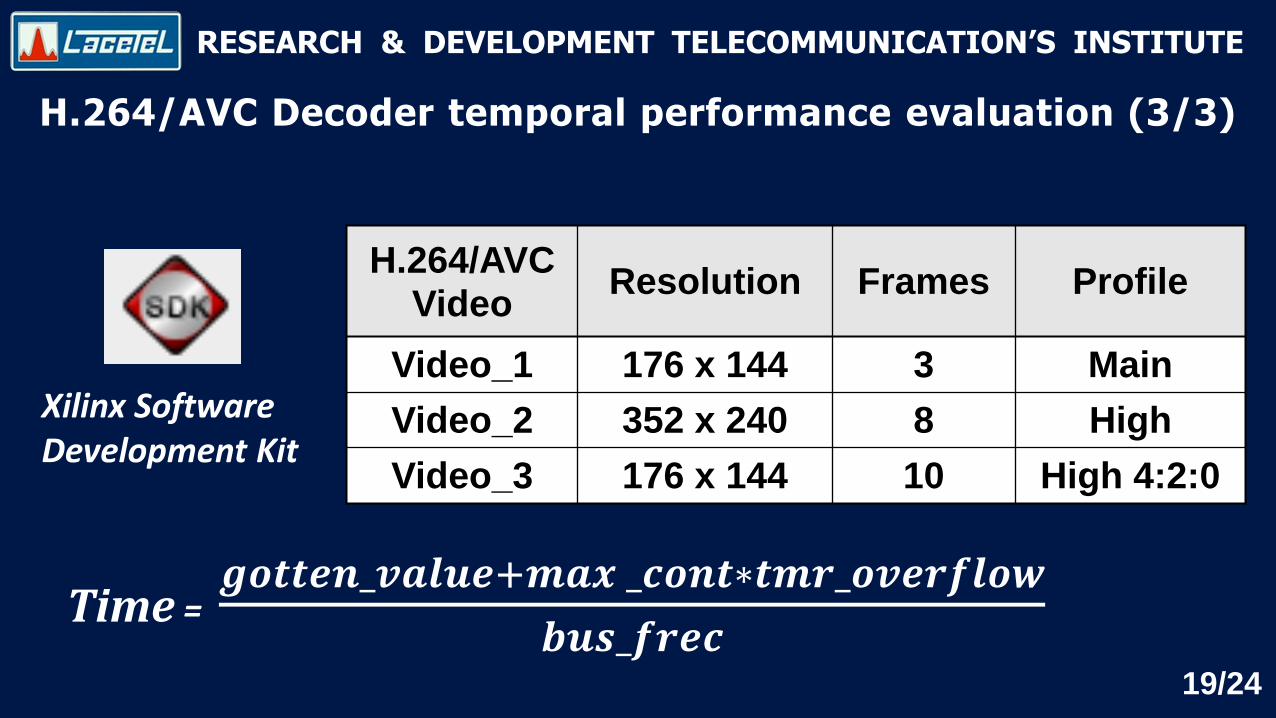
H.264/AVC Decoder temporal performance evaluation (3/3)
19/24
Xilinx Software Development Kit
H.264/AVC Video
Resolution Frames Profile
Video_1 176 x 144 3 Main
Video_2 352 x 240 8 High
Video_3 176 x 144 10 High 4:2:0
Time = 𝒈𝒐𝒕𝒕𝒆𝒏_𝒗𝒂𝒍𝒖𝒆+𝒎𝒂𝒙 _𝒄𝒐𝒏𝒕∗𝒕𝒎𝒓_𝒐𝒗𝒆𝒓𝒇𝒍𝒐𝒘
𝒃𝒖𝒔_𝒇𝒓𝒆𝒄

RESEARCH & DEVELOPMENT TELECOMMUNICATION’S INSTITUTE
Analysis of experiments results
20/2411750
11800
11850
11900
11950
12000
12050
Tim
e (
ms)
Results for Video_2
11 885
11 990
11 884
Experiment 1: Software H.264 Decoding Timing(previous work in LACETEL)
Experiment 2: Software/Hardware H.264 Decoding Timing (with Bypass Decoder IP module on)
Experiment 3: Software/Hardware H.264 Decoding Timing (with optimized Bypass Decoder IP module on)

RESEARCH & DEVELOPMENT TELECOMMUNICATION’S INSTITUTE
21/24
• The Interrupt controller and the Timer/Counter were added to the
embedded system in which the H.264/AVC model is implemented.
• The Bypass Decoder IP module was optimized and fitted into the
H.264/AVC decoder system.
• The H.264/AVC Decoder temporal performance was evaluated for
different designs and the results showed that the optimization of
Bypass Decoder IP module made possible to reduce decoding delay.
Conclusions (1/2)

RESEARCH & DEVELOPMENT TELECOMMUNICATION’S INSTITUTE
22/24
• A methodology of IP modules insertion into the H.264/AVC decoder in
an embedded system was build.
• The H.264/AVC decoder showed is a platform capable of supporting
next implementations such as the insertion of IP modules following
the way showed in this work.
Conclusions (2/2)

RESEARCH & DEVELOPMENT TELECOMMUNICATION’S INSTITUTE
23/24
• Introduce some IP modules into the H.264/AVC decoder system that
allow to visualize the decoded frames through interfaces such as VGA
or DVI.
• Time the delay produced by the rest of the elements in the
H.264/AVC Decoder System to find which of them need to be
optimized.
Next work

RESEARCH & DEVELOPMENT TELECOMMUNICATION’S INSTITUTE
DIGITAL
TELEVISION
LABORATORY

RESEARCH & DEVELOPMENT TELECOMMUNICATION’S INSTITUTE
www.lacetel.cu