austriamicrosystems ag is now ams ag · the rf power amplifier and avoids a system shutdown....
TRANSCRIPT

austriamicrosystems AG
is now
ams AGThe technical content of this austriamicrosystems datasheet is still valid.
Contact information:
Headquarters:ams AG
Tobelbaderstrasse 30
8141 Unterpremstaetten, Austria
Tel: +43 (0) 3136 500 0
e-Mail: [email protected]
Please visit our website at www.ams.com
AS3647/47B 1600mA High Current LED Flash Driver
www.austriamicrosystems.com/AS3647 1.5-4 1 - 37(ptr)
Datasheet
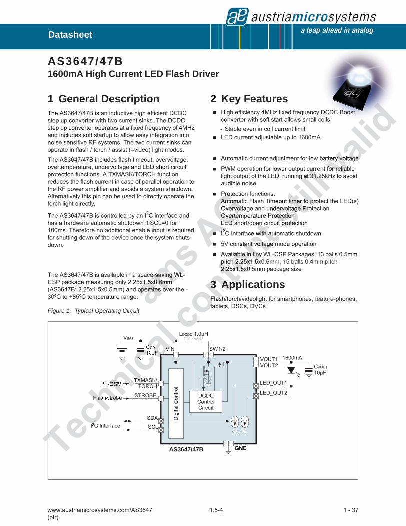
1 General DescriptionThe AS3647/47B is an inductive high efficient DCDC step up converter with two current sinks. The DCDC step up converter operates at a fixed frequency of 4MHz and includes soft startup to allow easy integration into noise sensitive RF systems. The two current sinks can operate in flash / torch / assist (=video) light modes.
The AS3647/47B includes flash timeout, overvoltage, overtemperature, undervoltage and LED short circuit protection functions. A TXMASK/TORCH function reduces the flash current in case of parallel operation to the RF power amplifier and avoids a system shutdown. Alternatively this pin can be used to directly operate the torch light directly.
The AS3647/47B is controlled by an I2C interface and has a hardware automatic shutdown if SCL=0 for 100ms. Therefore no additional enable input is required for shutting down of the device once the system shuts down.
The AS3647/47B is available in a space-saving WL-CSP package measuring only 2.25x1.5x0.6mm (AS3647B: 2.25x1.5x0.5mm) and operates over the -30ºC to +85ºC temperature range.
Figure 1. Typical Operating Circuit
2 Key FeaturesHigh efficiency 4MHz fixed frequency DCDC Boost converter with soft start allows small coils- Stable even in coil current limitLED current adjustable up to 1600mA
Automatic current adjustment for low battery voltage
PWM operation for lower output current for reliable light output of the LED; running at 31.25kHz to avoid audible noise
Protection functions:Automatic Flash Timeout timer to protect the LED(s)Overvoltage and undervoltage ProtectionOvertemperature ProtectionLED short/open circuit protection
I2C Interface with automatic shutdown
5V constant voltage mode operation
Available in tiny WL-CSP Packages, 13 balls 0.5mm pitch 2.25x1.5x0.6mm, 15 balls 0.4mm pitch 2.25x1.5x0.5mm package size
3 ApplicationsFlash/torch/videolight for smartphones, feature-phones, tablets, DSCs, DVCs
���������������
� ��
������
���� ������������
��
�����
��
���
�
� ! �"�#$
��%��
&��'�%��
(!�
&������)�*+
�� !
��*�
���%�
��*�
&��'�%�$
��,(�-�.-��/#
����+
(!�(!�(!�(!�
��%�$
���
��& $�� ����0��
AS3647/47B
ams
e-saving WL-e-saving WL-1.5x0.6mm 1.5x0.6mm
operates oveoperates ov
AGed
ProteroAutomatAutomaOvervoltagvervoltOvertemOvertemLED sLED s
II22C
Technica
l aacal
ccicicciill
����������
� �� !
��*�
l,(�-
�.nnnTTec
hnical
T
cconten
t pen cien c
ace with autowith auto
onstant voltage mtant voltage m
Available in tiny Wlable in tinypitch 2.25x1.5xpitch 2.25x1.5x2.25x1.5x0.2.25x1.5x0.
3 App3 AppFlasFlastatcc
still
currecurg at 31.25g at 31.2
eout timer to prottimer to prondervoltage Protervoltage Pro
Protectiontectiont protect protec
valid
battery voltagetery voltage
for reliablefor reliabz to a

www.austriamicrosystems.com/AS3647 1.5-4 2 - 37
AS3647/47BDatasheet, Confidential - P inou t
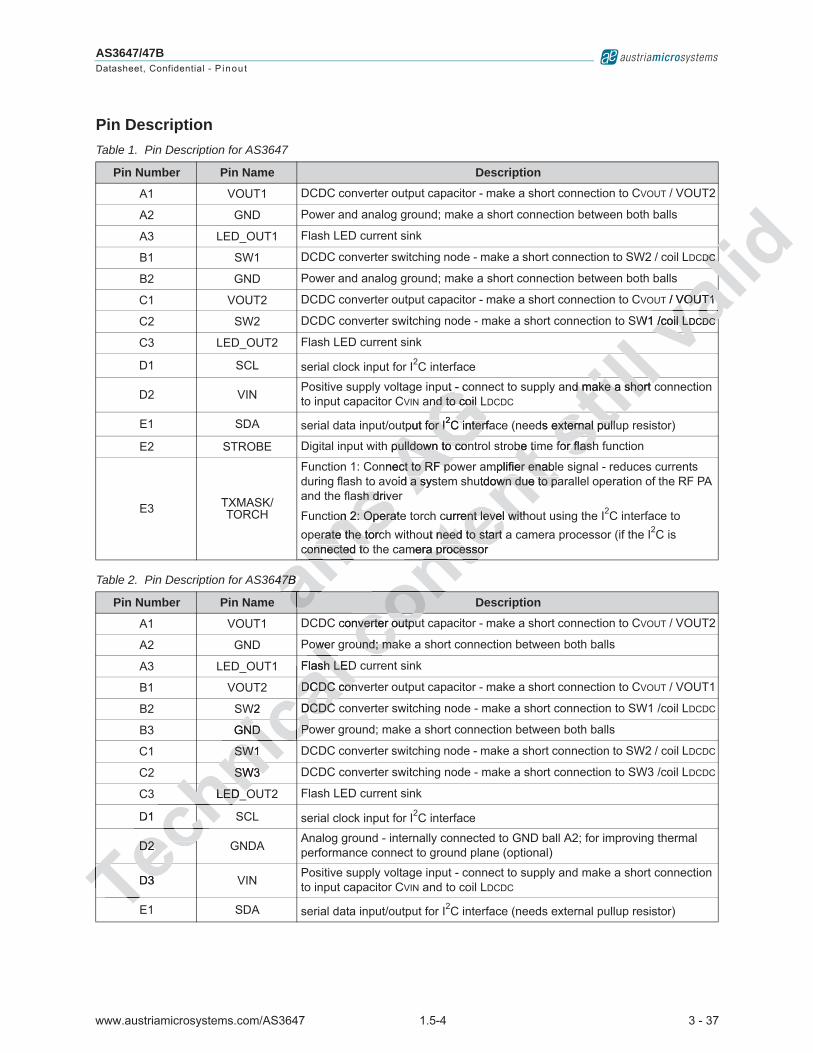
4 PinoutPin AssignmentFigure 2. Pin Assignments (Top View) AS3647
Figure 3. Pin Assignments (Top View) AS3647B
�����������
�������
����������
�������
�����
�����
���������� ����!�����#����� ��"#��"�$�� ����%���
����������
�����
�����
�����
�����
�����
����&���
���'(��)#��&�*
AS3647
�����������
��������
�� ������������� �������������������� �������!��"
�� ��� #����$�����������%��� ���& ����'%��(������'��%��)��'� �*��)�� ����+
���������
����
���$
,����
��-.�
$����
$-��
���
,-���
�����
,����
�����$
��/1$�2��3�4
���3�,�
AS3647B
amamamaaama��� msS3647BS3647Bms sssmm
AG AAGAGAGAGAGGGGGGGGGGGGGGGGGGGGGGGGGGGGGGAGAGAGAGAGAGAGAGAGAGAAAAAAAAAAAAAAAAAAAAAAAAGAGAGAGAGAGAGAGAGAGAGAGAGAGAGAAAAAAAAAAAAAAAAAAAGAAAAGAGAGAGAGAGAGAGAGAGAGAGAGGGGGGGGGGGGGGGGGG
���.�
���&������
���'�����
TeTechnicaca
l caacaa
laaaallalllalalllll---
Te
nteco
ntntonon
conococococooooooooonononononoooooo$����cccccccccccccccccccctenen
t nntten
AS36
tetesti
ll valali
dalial
www.austriamicrosystems.com/AS3647 1.5-4 3 - 37
AS3647/47BDatasheet, Confidential - P inou t
Pin DescriptionTable 1. Pin Description for AS3647
Pin Number Pin Name Description
A1 VOUT1 DCDC converter output capacitor - make a short connection to CVOUT / VOUT2
A2 GND Power and analog ground; make a short connection between both balls
A3 LED_OUT1 Flash LED current sink
B1 SW1 DCDC converter switching node - make a short connection to SW2 / coil LDCDC
B2 GND Power and analog ground; make a short connection between both balls
C1 VOUT2 DCDC converter output capacitor - make a short connection to CVOUT / VOUT1
C2 SW2 DCDC converter switching node - make a short connection to SW1 /coil LDCDC
C3 LED_OUT2 Flash LED current sink
D1 SCL serial clock input for I2C interface
D2 VINPositive supply voltage input - connect to supply and make a short connection to input capacitor CVIN and to coil LDCDC
E1 SDA serial data input/output for I2C interface (needs external pullup resistor)
E2 STROBE Digital input with pulldown to control strobe time for flash function
E3 TXMASK/TORCH
Function 1: Connect to RF power amplifier enable signal - reduces currents during flash to avoid a system shutdown due to parallel operation of the RF PA and the flash driver
Function 2: Operate torch current level without using the I2C interface to operate the torch without need to start a camera processor (if the I2C is connected to the camera processor
Table 2. Pin Description for AS3647B
Pin Number Pin Name Description
A1 VOUT1 DCDC converter output capacitor - make a short connection to CVOUT / VOUT2
A2 GND Power ground; make a short connection between both balls
A3 LED_OUT1 Flash LED current sink
B1 VOUT2 DCDC converter output capacitor - make a short connection to CVOUT / VOUT1
B2 SW2 DCDC converter switching node - make a short connection to SW1 /coil LDCDC
B3 GND Power ground; make a short connection between both balls
C1 SW1 DCDC converter switching node - make a short connection to SW2 / coil LDCDC
C2 SW3 DCDC converter switching node - make a short connection to SW3 /coil LDCDC
C3 LED_OUT2 Flash LED current sink
D1 SCL serial clock input for I2C interface
D2 GNDAAnalog ground - internally connected to GND ball A2; for improving thermal performance connect to ground plane (optional)
D3 VINPositive supply voltage input - connect to supply and make a short connection to input capacitor CVIN and to coil LDCDC
E1 SDA serial data input/output for I2C interface (needs external pullup resistor)
ams
o ash drivesh d
on 2: Operateon 2: Operaerate the torcerate the torc
connected toconnected to
647B47BaaamaaAG ut - co
nd to coil Lnd to coil
put for Ior I2C interfaC interf
h pulldown to conpulldown to con
nnect to RF poct to RF pid a sysa s
GAGA
TeD33TTecD2D2 cchD1 chchnLED_OLED_O
chhnica
l owerowe
Flash LEDsh LE
DCDC conDCDC con
W2 DCDCDCDC
GNDND PoP
SW1SW1
SW3SW3hca
lal caicnichnhn
chcTeT
conten
t obe timbe ti
mplifier enableer enablutdown due to paown due to pa
current level withent level witut need to start aneed to start
mera processora processor
con
converter outpunverter outpu
und; maund; ma
tnt
oncocc
still nd make a short cd make a short
ds external pulluexternal pullu
for flashfor flash
llillstissva
lidCDCDC
UT / VOUT1VOUT1
W1 /coil L/coil LDCDCCDCaliilialvavv

www.austriamicrosystems.com/AS3647 1.5-4 4 - 37
AS3647/47BDatasheet, Confidential - P inou t
E2 STROBE Digital input with pulldown to control strobe time for flash function
E3 TXMASK/TORCH
Function 1: Connect to RF power amplifier enable signal - reduces currents during flash to avoid a system shutdown due to parallel operation of the RF PA and the flash driver
Function 2: Operate torch current level without using the I2C interface to operate the torch without need to start a camera processor (if the I2C is connected to the camera processor
Table 2. Pin Description for AS3647B
Pin Number Pin Name Description
ams A
G
Technica
l conten
t still
validaliali
www.austriamicrosystems.com/AS3647 1.5-4 5 - 37
AS3647/47BDatasheet, Confidential - Abso lu te Max imum Rat ings
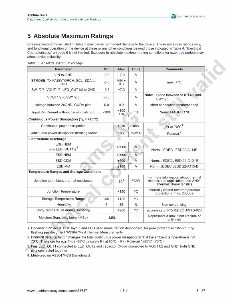
5 Absolute Maximum RatingsStresses beyond those listed in Table 3 may cause permanent damage to the device. These are stress ratings only, and functional operation of the device at these or any other conditions beyond those indicated in Table 4, “Electrical Characteristics,” on page 6 is not implied. Exposure to absolute maximum rating conditions for extended periods may affect device reliability.
Table 3. Absolute Maximum Ratings
Parameter Min Max Units CommentsVIN to GND -0.3 +7.0 V
STROBE, TXMASK/TORCH, SCL, SDA to GND -0.3 VIN +
0.3 V max. +7V
SW1/2/3, VOUT1/2, LED_OUT1/2 to GND -0.3 +7.0 V
VOUT1/2 to SW1/2/3 -0.3 VNote: Diode between VOUT1/2 and
SW1/2/3
voltage between 2xGND, GNDA pins 0.0 0.0 V short connection recommended
Input Pin Current without causing latchup -100 +100+IIN mA Norm: EIA/JESD78
Continuous Power Dissipation (TA = +70ºC)
Continuous power dissipation 1230 mW PT at 70ºC1
1. Depending on actual PCB layout and PCB used measured on demoboard; for peak power dissipation during flashing see document 'AS3647/47B Thermal Measurements'
Continuous power dissipation derating factor 16.7 mW/ºC PDERATE2
2. PDERATE derating factor changes the total continuous power dissipation (PT) if the ambient temperature is not 70ºC. Therefore for e.g. TAMB=85ºC calculate PT at 85ºC = PT - PDERATE * (85ºC - 70ºC)
Electrostatic DischargeESD HBM
pins LED_OUT1/23
3. Pins LED_OUT1 connected to LED_OUT2 and capacitor CVOUT connected to VOUT1/2 and GND; both GND pins connected together
±8000 VNorm: JEDEC JESD22-A114F
ESD HBM ±2000 V
ESD CDM ±500 V Norm: JEDEC JESD 22-C101E
ESD MM ±100 V Norm: JEDEC JESD 22-A115-BTemperature Ranges and Storage Conditions
Junction to ambient thermal resistance 604
4. Measured on AS3647/47B Demoboard.
ºC/WFor more information about thermal metrics, see application note AN01
Thermal Characteristics
Junction Temperature +150 ºC Internally limited (overtemperature protection), max. 20000s
Storage Temperature Range -55 +125 ºCHumidity 5 85 % Non condensing
Body Temperature during Soldering +260 ºC according to IPC/JEDEC J-STD-020
Moisture Sensitivity Level (MSL) MSL 1 Represents a max. floor life time of unlimited
ams
e ConCon
mssmsmamaAG NN m
1230 m1230 m
16.716.7AGAGGAGAGA
Techn
ng on actual PCBn actual PCng see documentee documen
ERATE derating fa derating 70ºC. Therefore 70ºC. Therefore
3. Pins LED_OU3. Pins LED_Opins connepins conne
4. Measureasu
hniSensitivity Level (tivity Level (nicre during Solderinng Solderinicatyy caRangenge al llacaicnihn
conten
t C
VV
2000 V0 V
±500 V±500 V
±100±100ocont nen
tntntentnoncoc
still
n
ction recommection recomm
Norm: EIA/JESDrm: EIA/JESD
PPTT a
llillstistsva
lidliUT1/2 and UT1/2 an
alililivava
www.austriamicrosystems.com/AS3647 1.5-4 6 - 37
AS3647/47BDatasheet, Confidential - E lec t r i ca l Charac te r is t i cs
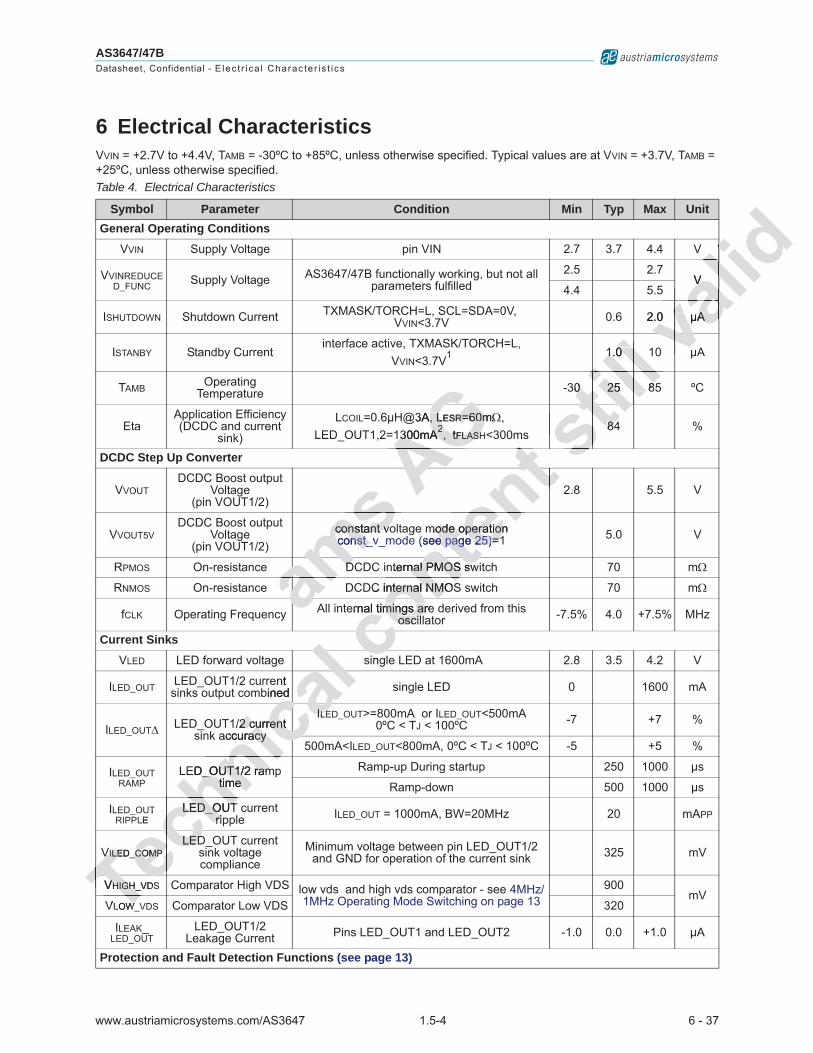
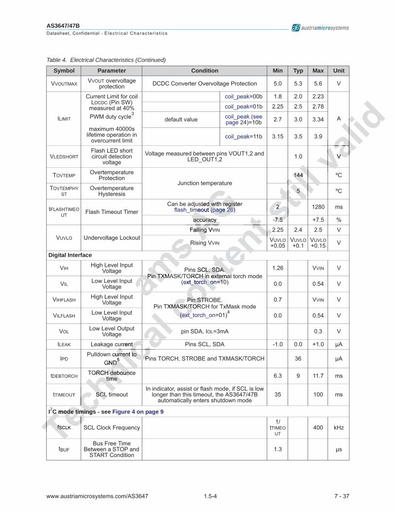
6 Electrical CharacteristicsVVIN = +2.7V to +4.4V, TAMB = -30ºC to +85ºC, unless otherwise specified. Typical values are at VVIN = +3.7V, TAMB = +25ºC, unless otherwise specified. Table 4. Electrical Characteristics
Symbol Parameter Condition Min Typ Max UnitGeneral Operating Conditions
VVIN Supply Voltage pin VIN 2.7 3.7 4.4 V
VVINREDUCED_FUNC Supply Voltage AS3647/47B functionally working, but not all
parameters fulfilled2.5 2.7
V4.4 5.5
ISHUTDOWN Shutdown Current TXMASK/TORCH=L, SCL=SDA=0V, VVIN<3.7V 0.6 2.0 μA
ISTANBY Standby Currentinterface active, TXMASK/TORCH=L,
VVIN<3.7V1 1.0 10 μA
TAMB Operating Temperature -30 25 85 ºC
EtaApplication Efficiency (DCDC and current
sink)
LCOIL=0.6μH@3A, LESR=60m , LED_OUT1,2=1300mA2, tFLASH<300ms
84 %
DCDC Step Up Converter
VVOUTDCDC Boost output
Voltage (pin VOUT1/2)
2.8 5.5 V
VVOUT5VDCDC Boost output
Voltage (pin VOUT1/2)
constant voltage mode operation const_v_mode (see page 25)=1 5.0 V
RPMOS On-resistance DCDC internal PMOS switch 70 m
RNMOS On-resistance DCDC internal NMOS switch 70 m
fCLK Operating Frequency All internal timings are derived from this oscillator -7.5% 4.0 +7.5% MHz
Current SinksVLED LED forward voltage single LED at 1600mA 2.8 3.5 4.2 V
ILED_OUT LED_OUT1/2 current sinks output combined single LED 0 1600 mA
ILED_OUT LED_OUT1/2 current sink accuracy
ILED_OUT>=800mA or ILED_OUT<500mA0ºC < TJ < 100ºC -7 +7 %
500mA<ILED_OUT<800mA, 0ºC < TJ < 100ºC -5 +5 %
ILED_OUTRAMP
LED_OUT1/2 ramp time
Ramp-up During startup 250 1000 μs
Ramp-down 500 1000 μs
ILED_OUTRIPPLE
LED_OUT current ripple ILED_OUT = 1000mA, BW=20MHz 20 mAPP
VILED_COMPLED_OUT current
sink voltage compliance
Minimum voltage between pin LED_OUT1/2 and GND for operation of the current sink 325 mV
VHIGH_VDS Comparator High VDS low vds and high vds comparator - see 4MHz/1MHz Operating Mode Switching on page 13
900mV
VLOW_VDS Comparator Low VDS 320
ILEAK_LED_OUT
LED_OUT1/2 Leakage Current Pins LED_OUT1 and LED_OUT2 -1.0 0.0 +1.0 μA
Protection and Fault Detection Functions (see page 13)
aaamaams constant voconstant vo
const_vconst_
DDasmama
AG@3A, LA, LESRR=60m=60m1300mA1300mA22, t, tFLASHFLASHGAGA
TVLOW_WTecVVILED_COMPILED_COMPLEDLED
VVHIGH_VDSHIGHTecechUT
LELED_OUTLED_OUT
riri
echni
LED_OUT1/2 ram_OUT1/2 ramtimetimenica1/2 current 2 current accuracyacy
IILELEcacal ent
bined
caalallalcacni
hecTeT
cingcon
ernal timings arel timings arosciloscilonC internal NMOSnternal NMOonten
t mode operation ode operation
(see page 25)e page 25)=1=1
ternal PMOS swnal PMOS sw
tttennt
ononcoc
still 1.0 11.0
30 25 80 25 8
8484sstillilltis
validVV
2.0 μAμAvaliliav
www.austriamicrosystems.com/AS3647 1.5-4 7 - 37
AS3647/47BDatasheet, Confidential - E lec t r i ca l Charac te r is t i cs
VVOUTMAX VVOUT overvoltage protection DCDC Converter Overvoltage Protection 5.0 5.3 5.6 V
ILIMIT
Current Limit for coil LDCDC (Pin SW)
measured at 40% PWM duty cycle3
maximum 40000s lifetime operation in
overcurrent limit
coil_peak=00b 1.8 2.0 2.23
A
coil_peak=01b 2.25 2.5 2.78
default value coil_peak (see page 24)=10b 2.7 3.0 3.34
coil_peak=11b 3.15 3.5 3.9
VLEDSHORTFlash LED short circuit detection
voltageVoltage measured between pins VOUT1,2 and
LED_OUT1,2 1.0 V
TOVTEMP Overtemperature Protection
Junction temperature144 ºC
TOVTEMPHYST
Overtemperature Hysteresis 5 ºC
tFLASHTIMEOUT Flash Timeout Timer
Can be adjusted with register flash_timeout (page 26) 2 1280 ms
accuracy -7.5 +7.5 %
VUVLO Undervoltage LockoutFalling VVIN 2.25 2.4 2.5 V
Rising VVIN VUVLO+0.05
VUVLO+0.1
VUVLO+0.15 V
Digital Interface
VIH High Level Input Voltage Pins SCL, SDA.
Pin TXMASK/TORCH in external torch mode (ext_torch_on=10)
1.26 VVIN V
VIL Low Level Input Voltage 0.0 0.54 V
VIHFLASH High Level Input Voltage Pin STROBE.
Pin TXMASK/TORCH for TxMask mode (ext_torch_on=01)4
0.7 VVIN V
VILFLASH Low Level Input Voltage 0.0 0.54 V
VOL Low Level Output Voltage pin SDA, IOL=3mA 0.3 V
ILEAK Leakage current Pins SCL, SDA -1.0 0.0 +1.0 μA
IPDPulldown current to
GND5 Pins TORCH, STROBE and TXMASK/TORCH 36 μA
tDEBTORCH TORCH debounce time 6.3 9 11.7 ms
tTIMEOUT SCL timeoutIn indicator, assist or flash mode, if SCL is low
longer than this timeout, the AS3647/47B automatically enters shutdown mode
35 100 ms
I2C mode timings - see Figure 4 on page 9
fSCLK SCL Clock Frequency1/
tTIMEOUT
400 kHz
tBUFBus Free Time
Between a STOP and START Condition
1.3 μs
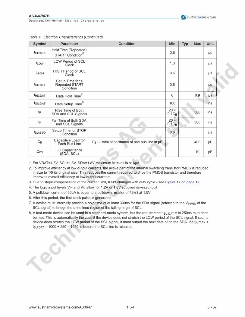
Table 4. Electrical Characteristics (Continued)
Symbol Parameter Condition Min Typ Max Unit
aaams
Pin TXMAPin TXMAams R
msmsaa
AAFalling Vlling VAGaccuracyaccuracyAGsted with registed with registmeout (page 26)meout (page 26)G
at
GAGAA
TeffSCLKSTeTecC mode timingsC mode timingsechn
UT SCL timSCL
echniORCH debounceH debounc
timetimenicacurrent to urrent to GNDD5 PPcaica
rrentt cacal
call
caicanihn
ecTeT
coPin STRPin STRTXMASK/TORMASK/T
((ext_ext_onteSCL, SDA.L, SDA.
ORCH in externaH in externaext_torch_on_torch_o =10=10
tenttnt 2ttttnt
enteo
s-7.57.5ssti22sstistill55
stillill
144144
illlllillstisvvva
lidVVva
liav
www.austriamicrosystems.com/AS3647 1.5-4 8 - 37
AS3647/47BDatasheet, Confidential - E lec t r i ca l Charac te r is t i cs
tHD:STAHold Time (Repeated)
START Condition6 0.6 μs
tLOWLOW Period of SCL
Clock 1.3 μs
tHIGHHIGH Period of SCL
Clock 0.6 μs
tSU:STASetup Time for a Repeated START
Condition0.6 μs
tHD:DAT Data Hold Time7 0 0.9 μs
tSU:DAT Data Setup Time8 100 ns
tR Rise Time of Both SDA and SCL Signals
20 + 0.1CB
300 ns
tF Fall Time of Both SDA and SCL Signals
20 + 0.1CB
300 ns
tSU:STOSetup Time for STOP
Condition 0.6 μs
CBCapacitive Load for
Each Bus Line CB — total capacitance of one bus line in pF 400 pF
CI/OI/O Capacitance
(SDA, SCL) 10 pF
1. For VBAT=4.5V, SCL=1.8V, SDA=1.8V maximum ISTANBY is <16μA.2. To improve efficiency at low output currents, the active part of the internal switching transistor PMOS is reduced
in size to 1/5 its original size. This reduces the current required to drive the PMOS transistor and therefore improves overall efficiency at low output currents.
3. Due to slope compensation of the current limit, ILIMIT changes with duty cycle - see Figure 17 on page 12.4. The logic input levels VIH and VIL allow for 1.2V or 1.8V supplied driving circuit5. A pulldown current of 36μA is equal to a pulldown resistor of 42k at 1.5V6. After this period, the first clock pulse is generated.7. A device must internally provide a hold time of at least 300ns for the SDA signal (referred to the VIHMIN of the
SCL signal) to bridge the undefined region of the falling edge of SCL.8. A fast-mode device can be used in a standard-mode system, but the requirement tSU:DAT = to 250ns must then
be met. This is automatically the case if the device does not stretch the LOW period of the SCL signal. If such a device does stretch the LOW period of the SCL signal, it must output the next data bit to the SDA line tR max + tSU:DAT = 1000 + 250 = 1250ns before the SCL line is released.
Table 4. Electrical Characteristics (Continued)
Symbol Parameter Condition Min Typ Max Unit
V maximum Imaximum currents, the urrents, the
is reduces ths reduces tow output cuw output c
currecurre
ms sms AG acitance of oance of o
GAGAGA
Technica
la pe is genergene
a hold time of aold time of efined region of tregion of t
used in a sted in a standaandically the case if tcally the case
he LOW period oW period o250 = 1250ns bef= 1250ns be
conteis <16μA.6μA.
part of the internaof the internnt required to driquired to d
, ILIMITT changes w change.2V or 1.8V supV or 1.8V sup
own resistown resisd
tent s line in pFe in pFttnt
tensti
llCB300300
20 + + 0.1C1CBB
0.60.6sstilllltilsts
validμsμs
0.9 μss
nnvalili
vavv
www.austriamicrosystems.com/AS3647 1.5-4 9 - 37
AS3647/47BDatasheet, Confidential - E lec t r i ca l Charac te r is t i cs
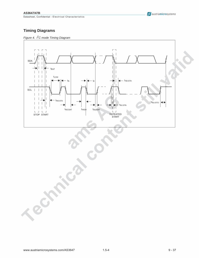
Timing Diagrams
Figure 4. I2C mode Timing Diagram
SCL
SDA
tBUF
tHD:STA
tSU:STA
REPEATED START
tSU:STO
tF
tSU:DATtHIGHtHD:DAT
tR
tLOW
tHD:STA
STARTSTOP
ams ms AG GGGGGGGGGGGGGGGGAGAGAGAGt
RRAU:DATDAT
Technica
l conten
t D T
tensti
lltiltilltilll ll
ttS
ll valvvvvalidal
www.austriamicrosystems.com/AS3647 1.5-4 10 - 37
AS3647/47BDatasheet, Confidential - Typ ica l Opera t ing Charac te r i s t i cs
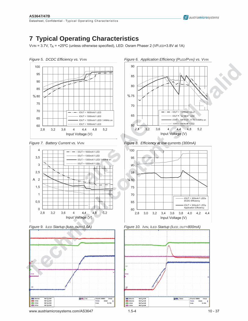
7 Typical Operating CharacteristicsVVIN = 3.7V, TA = +25ºC (unless otherwise specified), LED: Osram Phaser 2 (VFLED=3.8V at 1A)
Figure 5. DCDC Efficiency vs. VVIN Figure 6. Application Efficiency (PLED/PVIN) vs. VVIN
60
65
70
75
80
85
90
95
100
2,8 3,2 3,6 4 4,4 4,8 5,2
%
Input Voltage (V)
IOUT = 1600mA/1 LED
IOUT = 1300mA/1 LED
IOUT = 1300mA/1 LED/ 1/4MHz on
IOUT = 1000mA/1 LED 60
65
70
75
80
85
90
2,8 3,2 3,6 4 4,4 4,8 5,2
%
Input Voltage (V)
IOUT = 1600mA/1 LED
IOUT = 1300mA/1 LED
IOUT = 1300mA/1 LED/ 1/4MHz on
IOUT = 1000mA/1 LED
Figure 7. Battery Current vs. VVIN Figure 8. Efficiency at low currents (300mA)
0
0,5
1
1,5
2
2,5
3
3,5
4
2,8 3,2 3,6 4 4,4 4,8 5,2
A
Input Voltage (V)
IOUT = 1600mA/1 LED
IOUT = 1300mA/1 LED
IOUT = 1300mA/1 LED/ 1/4MHz on
IOUT = 1000mA/1 LED
60
65
70
75
80
85
90
95
100
2,8 3,0 3,2 3,4 3,6 3,8 4,0 4,2 4,4
%
Input Voltage (V)
IOUT = 300mA/1 LEDsDCDC Efficiency
IOUT = 300mA/1 LEDsApplication Efficiency
Figure 9. ILED Startup (ILED_OUT=1.0A) Figure 10. IVIN, ILED Startup (ILED_OUT=800mA)
ams
amamamamamamamammmaamsmsms1/4MHz
ED s ss AAGAAAAG GGGGGGGGGG602,8 3,2
AGAGFigure 8Figure 8AA
Technicica
l alalllalalalalalalalal4 4,8 5Voltage (V)icic(ILED_OUTED_OUT=1.0A)=1.0A)
Tni
cocccccccccccccccococoontententententenn
tntennten
tntnttetennnnntententetetentntntntnt nt tttency y at low cuat low cu
80
85
0
%ontent
ontent ssti
llllllllllll4,4 4
Voltage still
still
still600mA/1 LED
1300mA/1 LED
UT = 1300mA/1 LED/ 1/
T = 1000mA/1 LE
ssva
lidvavvvvvvvvvvvvvvvvvava

www.austriamicrosystems.com/AS3647 1.5-4 11 - 37
AS3647/47BDatasheet, Confidential - Typ ica l Opera t ing Charac te r i s t i cs
Figure 11. ILED Startup (ILED_OUT=60mA) Figure 12. VOUT / ILED_OUT ripple, ILED_OUT = 1.0A
Figure 13. ILED Rampdown (ILED_OUT=1.0A) Figure 14. ILED_OUT vs. TAMB
58
59
60
61
62
63
-30 -10 10 30 50 70
mA
Ambient Temperature (C)
Figure 15. Oscillator frequency fCLK vs. TAMB Figure 16. Flash Timeout
3.8
3.9
4.0
4.1
4.2
-30 -10 10 30 50 70
MHz
Ambient Temperature (C)
s s AG GFigure 14. Iure 14. ILED_LED
AGGGGG6AGAG
Tech
ececech
echccechnihh
echni
echni
chni
chninic
Techni
Techni
TeTeech
ech
Technicaa
luency fency CLKCLKf vs. T vs. KK
3.9Technic
Technic
coconten
t nten
tnten
tten
tten
ten
ten
tnten
tnten
tntnten
ten
t60
61
oo
stiltilTAMBMBT sssssss
valid
va
www.austriamicrosystems.com/AS3647 1.5-4 12 - 37
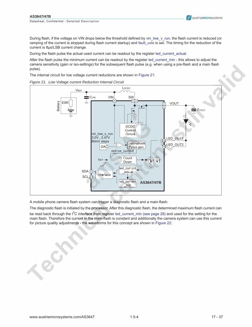
AS3647/47BDatasheet, Confidential - Deta i led Descr ip t ion
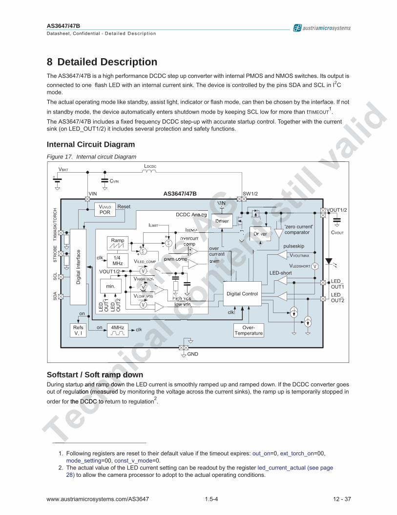
8 Detailed DescriptionThe AS3647/47B is a high performance DCDC step up converter with internal PMOS and NMOS switches. Its output is connected to one flash LED with an internal current sink. The device is controlled by the pins SDA and SCL in I2C mode.
The actual operating mode like standby, assist light, indicator or flash mode, can then be chosen by the interface. If not
in standby mode, the device automatically enters shutdown mode by keeping SCL low for more than tTIMEOUT1.
The AS3647/47B includes a fixed frequency DCDC step-up with accurate startup control. Together with the current sink (on LED_OUT1/2) it includes several protection and safety functions.
Internal Circuit DiagramFigure 17. Internal circuit Diagram
Softstart / Soft ramp downDuring startup and ramp down the LED current is smoothly ramped up and ramped down. If the DCDC converter goes out of regulation (measured by monitoring the voltage across the current sinks), the ramp up is temporarily stopped in
order for the DCDC to return to regulation2.
1. Following registers are reset to their default value if the timeout expires: out_on=0, ext_torch_on=00, mode_setting=00, const_v_mode=0.
2. The actual value of the LED current setting can be readout by the register led_current_actual (see page 28) to allow the camera processor to adopt to the actual operating conditions.
����
���
��
�����
� ���������
����������������
��� �� �!
��"� �!
��#�"�
$�
�"���
%�
��&��
��&��
���"���
�������
�'��
��������(���(�
)*��(��+�����)�(,-����(�
-+�'�'.�-
������
(&���+�����
/��* ��. �&��0��,-����+��
(�
��"� �! �
����#���%
��#
�"�
-1,��(,-��.
�,-
2
2
-1,
������
2
0
(&���+���(,-
��'�3��
���
(� ��.
�������(�
�
� �(1�&4'
5��5�&4'
���
����
���"�
�/���*
,��6
��#
�"�!
��#�"�!
�
��0'5(��
���$�#��
����#��
AS3647/47B
ams
amammams
amaaaam-1,��(,-
mssmssssss�(,aa�aa��$�#��
� ��
GAG GAGAGGGGAAGAGAGAGG�����(�
Technicoft ramp dowamp do
p and ramp down and ramp downation (measured n (measured
or the DCDC to reDCDC to re
Tnicaca
l ca
lnic
ccocccoonten
t
conon
nnnnntntnt��&��tttttnnt nenn
tntentente
ooooo1,
tn
coco�(1�&4
4'
till
stistissstssvva
lidvv

www.austriamicrosystems.com/AS3647 1.5-4 13 - 37
AS3647/47BDatasheet, Confidential - Deta i led Descr ip t ion
4MHz/1MHz Operating Mode SwitchingIf freq_switch_on (see page 28)=1 and in flash and assist light mode (indicator mode or low current mode using PWM mode -see mode_setting (page 26) - always will use pulseskip) if led_current>=40h , the DCDC converter always oper-ates in PWM mode (exception: PFM mode is allowed during startup) to reduce EMI in EMI sensitive systems. For flash and assist light mode and high duty cycles close to 100% on-time (maximum duty cycle) of the PMOS, the DCDC con-
verter can switch into a 1MHz operating mode and maximum duty cycle to improve efficiency for this load condition3. The DCDC converter returns back to its normal 4MHz operating frequency when load or supply conditions change. Due to this switching between two fixed frequencies the noise spectrum of the system is exactly defined and predict-able. If improved efficiency is required, the fixed switching between 1MHz / 4MHz can be disabled by freq_switch_on (see page 28)=0. In this case pulseskip will be used.
The internal circuit for switching between these two frequencies is shown in Figure 18:
Figure 18. Internal circuit of 4MHz/1Mhz selection
Note: For simplicity Figure 18 shows only a single current sink.
Protection and Fault Detection FunctionsThe protection functions protect the AS3647/47B and the LED(s) against physical damage. In most cases a Fault reg-ister bit is set, which can be readout by the I2C interface. The fault bits are automatically cleared by a I2C readout of the
fault register. Additionally the DCDC is stopped and the current sinks are disabled4 by resetting out_on=0, mode_setting=00 and ext_torch_on=00.
Overvoltage ProtectionIn case of no or a broken LED(s) at the pin LED_OUT1/2 and an enabled DCDC converter, the voltage on VOUT1/2
rises until it reaches VVOUTMAX (overvoltage condition) and the voltage across the current source is below low_vds5.,
the DCDC converter is stopped, the current sources are disabled and the bit fault_ovp (see page 27) is set6.
3. Efficiency compared to a 4MHz only DCDC converter forced to operate with minimum duty cycle.4. Applies for all faults except TXMASK event occurred5. If overvoltage is reached, but none of the low_vds comparator(s) triggers, VOUT1/2 is still regulated below
VVOUTMAX.6. In constant voltage mode (5V generation, register bit const_v_mode=1) this fault is disabled.
����������
����
�
�
�����
���
�����
�������
���������������������
!
"���#
��#
�$%&���
�����'&�
��()���**+!,����-.
�����
���
�%/�"(0
$1��%/�"����$1��%/�0
&"(0
��%/���2
%3� �$1���������4�56�����37
AS3647/47B
as ons oamams
ammsms
�������
s msms)���**����-.
��
aAGGAAAAAAAAAAGGGGGGGGGAGG��%/�GAAAGAGAGAAG%3� �$1������A
Technica
lon onS3647/47B47/47
ut by the Iy the I22C inteC inte
DCDC is stDC is stoppedoppedorch_onorch_on=00.=00.
ctiononbroken LED(s) aten LED(s) at
ches Vches VVOUTMAXVOUTMA
converter is stopverter is stop
TT3.
con
ngle current sinke current sin
nctionsnctiond t
ontent
ontent
ontentt
enententeneettttnt
ettetententntntntntn����� ntnttte
��
$1��
37
on
still
stististststtssssstsst0
vavalidon on
vavaa
www.austriamicrosystems.com/AS3647 1.5-4 14 - 37
AS3647/47BDatasheet, Confidential - Deta i led Descr ip t ion
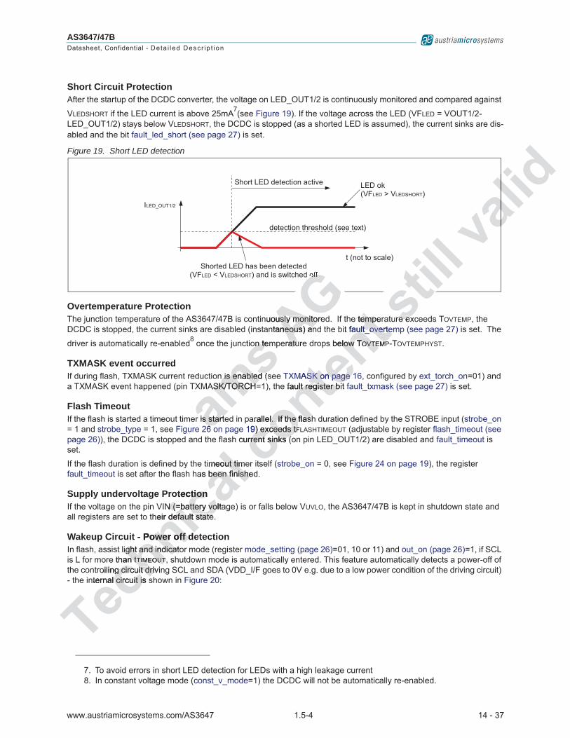
Short Circuit ProtectionAfter the startup of the DCDC converter, the voltage on LED_OUT1/2 is continuously monitored and compared against
VLEDSHORT if the LED current is above 25mA7(see Figure 19). If the voltage across the LED (VFLED = VOUT1/2-LED_OUT1/2) stays below VLEDSHORT, the DCDC is stopped (as a shorted LED is assumed), the current sinks are dis-abled and the bit fault_led_short (see page 27) is set.
Figure 19. Short LED detection
Overtemperature ProtectionThe junction temperature of the AS3647/47B is continuously monitored. If the temperature exceeds TOVTEMP, the DCDC is stopped, the current sinks are disabled (instantaneous) and the bit fault_overtemp (see page 27) is set. The
driver is automatically re-enabled8 once the junction temperature drops below TOVTEMP-TOVTEMPHYST.
TXMASK event occurredIf during flash, TXMASK current reduction is enabled (see TXMASK on page 16, configured by ext_torch_on=01) and a TXMASK event happened (pin TXMASK/TORCH=1), the fault register bit fault_txmask (see page 27) is set.
Flash TimeoutIf the flash is started a timeout timer is started in parallel. If the flash duration defined by the STROBE input (strobe_on = 1 and strobe_type = 1, see Figure 26 on page 19) exceeds tFLASHTIMEOUT (adjustable by register flash_timeout (see page 26)), the DCDC is stopped and the flash current sinks (on pin LED_OUT1/2) are disabled and fault_timeout is set.
If the flash duration is defined by the timeout timer itself (strobe_on = 0, see Figure 24 on page 19), the register fault_timeout is set after the flash has been finished.
Supply undervoltage ProtectionIf the voltage on the pin VIN (=battery voltage) is or falls below VUVLO, the AS3647/47B is kept in shutdown state and all registers are set to their default state.
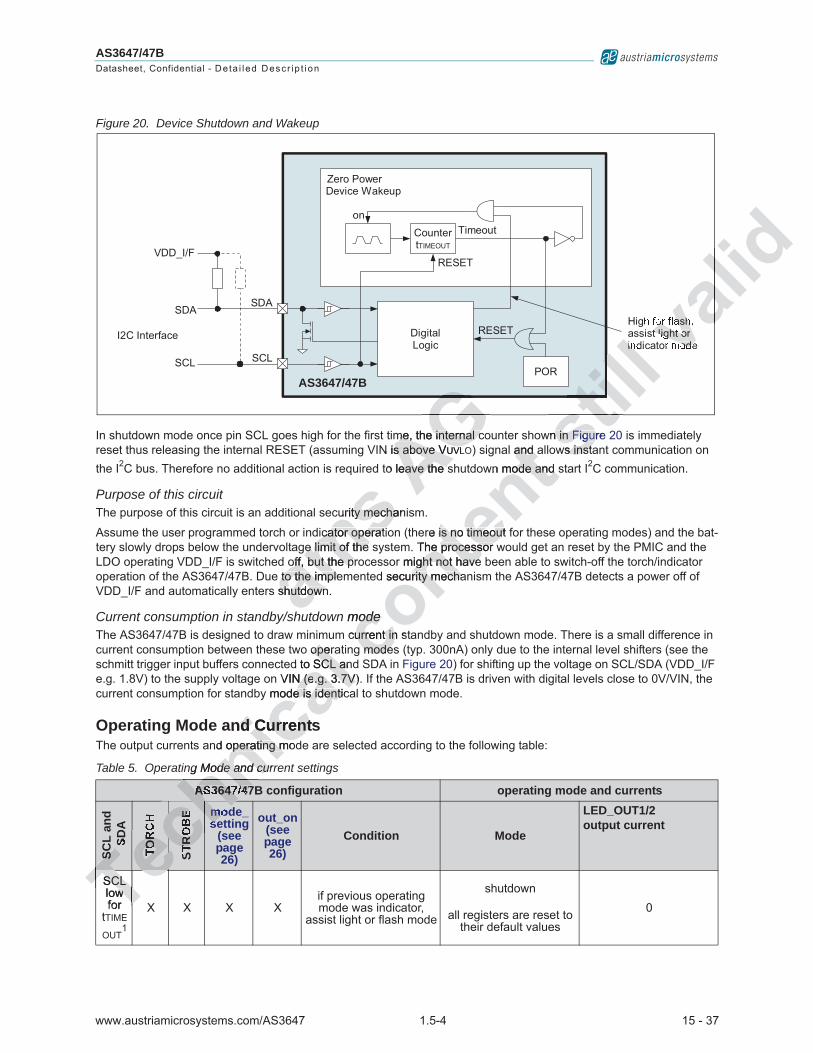
Wakeup Circuit - Power off detectionIn flash, assist light and indicator mode (register mode_setting (page 26)=01, 10 or 11) and out_on (page 26)=1, if SCL is L for more than tTIMEOUT, shutdown mode is automatically entered. This feature automatically detects a power-off of the controlling circuit driving SCL and SDA (VDD_I/F goes to 0V e.g. due to a low power condition of the driving circuit) - the internal circuit is shown in Figure 20:
7. To avoid errors in short LED detection for LEDs with a high leakage current8. In constant voltage mode (const_v_mode=1) the DCDC will not be automatically re-enabled.
��������������
� ���������
������� ������������������ ������ ������������� ���! ������""
������ ������� ������ # ����$��� ���%�� ��������
���� ���������������&��
ams on temon te
n is enabled (s is enabled ASK/SK/TORCH=TORCH=
r is startes start6 o6
AGuously monitoreusly monitorntaneous) anneous) an
raturatu
G �""
G
Technica
limeout timeout timas been finishebeen finishe
otectionctionIN (=battery voltaN (=battery vo
heir default stateefault state
t - Power off deower off dlight and indicatoight and indica
e than tn tTIMEOUTTIMEOUT solling circuit driving circuit driv
nternal circuit is scircuit i
conten
t e temperempebit fault_overtemault_overte
s below Tlow TOVTEMPOVTE
MASK on page 1SK on page fault register bit ult register b
arallel. If the flashl. If the flase 19) exceeds t) exceeds tFLFcurrent rrent sinks (sinks (
se
stre exe exstill
stva
lalid
alial
www.austriamicrosystems.com/AS3647 1.5-4 15 - 37
AS3647/47BDatasheet, Confidential - Deta i led Descr ip t ion
Figure 20. Device Shutdown and Wakeup
In shutdown mode once pin SCL goes high for the first time, the internal counter shown in Figure 20 is immediately reset thus releasing the internal RESET (assuming VIN is above VUVLO) signal and allows instant communication on the I2C bus. Therefore no additional action is required to leave the shutdown mode and start I2C communication.
Purpose of this circuitThe purpose of this circuit is an additional security mechanism.
Assume the user programmed torch or indicator operation (there is no timeout for these operating modes) and the bat-tery slowly drops below the undervoltage limit of the system. The processor would get an reset by the PMIC and the LDO operating VDD_I/F is switched off, but the processor might not have been able to switch-off the torch/indicator operation of the AS3647/47B. Due to the implemented security mechanism the AS3647/47B detects a power off of VDD_I/F and automatically enters shutdown.
Current consumption in standby/shutdown modeThe AS3647/47B is designed to draw minimum current in standby and shutdown mode. There is a small difference in current consumption between these two operating modes (typ. 300nA) only due to the internal level shifters (see the schmitt trigger input buffers connected to SCL and SDA in Figure 20) for shifting up the voltage on SCL/SDA (VDD_I/F e.g. 1.8V) to the supply voltage on VIN (e.g. 3.7V). If the AS3647/47B is driven with digital levels close to 0V/VIN, the current consumption for standby mode is identical to shutdown mode.
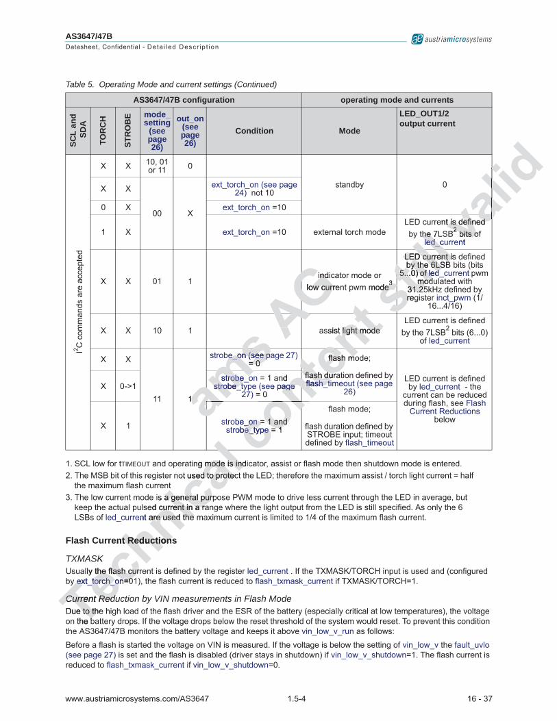
Operating Mode and CurrentsThe output currents and operating mode are selected according to the following table:
Table 5. Operating Mode and current settings
AS3647/47B configuration operating mode and currents
SCL
and
SD
A
TOR
CH
STR
OB
E mode_setting
(see page 26)
out_on (see page 26)
Condition Mode
LED_OUT1/2 output current
SCL low for
tTIME
OUT1
X X X Xif previous operating mode was indicator,
assist light or flash mode
shutdown
all registers are reset to their default values
0
�����������
����
��� ���
������
��������������������������������������������������������������������������������������������������������������������������������������������������������
������������ � � !
��������!�" #$!
� � !
!�%����
��
�#�
&��'��������(')�((�(�����'������*������%�*��
AS3647/47B
amsurity mechanty mecha
icator operatiicator operatie limit of the e limit of the
off, but the proff, but the pe to the impleto the impleshutdownshutdown
h
AG me, the internal cme, the internal c
N is above Vs above VUVLO
to leave the seave the sGGGG
Technica
l operaoperd to SCL andCL a
VIN (eN (e.g. 3.7V).g. 3.7Vy mode is identice is identi
and Currentsd Currentnd operating modoperating m
ng Mode and currde and cur
chnAS3647/47
TeS
TecTORech
TRO
BEchmse
SCL SCL low wfor
ETTeecchhn
chTe
conten
t l and aand awn mode and smode and
re is no timeoutis no timeout f. The processor he processor
r might not haveght not haved security mecharity mecha
n modeodecurrent in sturrent in
modemodeD
stwn in n in FigureFigurws instas inststi
ll tiltil��
stva
l�������('�����'����
%�*�
alid
alial
www.austriamicrosystems.com/AS3647 1.5-4 16 - 37
AS3647/47BDatasheet, Confidential - Deta i led Descr ip t ion
Flash Current Reductions
TXMASKUsually the flash current is defined by the register led_current . If the TXMASK/TORCH input is used and (configured by ext_torch_on=01), the flash current is reduced to flash_txmask_current if TXMASK/TORCH=1.
Current Reduction by VIN measurements in Flash ModeDue to the high load of the flash driver and the ESR of the battery (especially critical at low temperatures), the voltage on the battery drops. If the voltage drops below the reset threshold of the system would reset. To prevent this condition the AS3647/47B monitors the battery voltage and keeps it above vin_low_v_run as follows:
Before a flash is started the voltage on VIN is measured. If the voltage is below the setting of vin_low_v the fault_uvlo (see page 27) is set and the flash is disabled (driver stays in shutdown) if vin_low_v_shutdown=1. The flash current is reduced to flash_txmask_current if vin_low_v_shutdown=0.
I2 C c
omm
ands
are
acc
epte
d
X X 10, 01 or 11 0
standby 0X X
00 X
ext_torch_on (see page 24) not 10
0 X ext_torch_on =10
1 X ext_torch_on =10 external torch modeLED current is defined by the 7LSB2 bits of
led_current
X X 01 1indicator mode or
low current pwm mode3
LED current is defined by the 6LSB bits (bits
5...0) of led_current pwm modulated with
31.25kHz defined by register inct_pwm (1/
16...4/16)
X X 10 1 assist light modeLED current is defined
by the 7LSB2 bits (6...0) of led_current
X X
11 1
strobe_on (see page 27) = 0
flash mode;
flash duration defined by flash_timeout (see page
26)LED current is defined by led_current - the
current can be reduced during flash, see Flash
Current Reductions below
X 0->1strobe_on = 1 and
strobe_type (see page 27) = 0
X 1 strobe_on = 1 and strobe_type = 1
flash mode;
flash duration defined by STROBE input; timeout defined by flash_timeout
1. SCL low for tTIMEOUT and operating mode is indicator, assist or flash mode then shutdown mode is entered.2. The MSB bit of this register not used to protect the LED; therefore the maximum assist / torch light current = half
the maximum flash current3. The low current mode is a general purpose PWM mode to drive less current through the LED in average, but
keep the actual pulsed current in a range where the light output from the LED is still specified. As only the 6 LSBs of led_current are used the maximum current is limited to 1/4 of the maximum flash current.
Table 5. Operating Mode and current settings (Continued)
AS3647/47B configuration operating mode and currents
SCL
and
SD
A
TOR
CH
STR
OB
E mode_setting
(see page 26)
out_on (see page 26)
Condition Mode
LED_OUT1/2 output current
am1 amstrobe_otrobe_o
strobe_tstrobe_tams be_on (see pae_on (see p
= 0= 0ssmaAAAAG
indindlow curreow curr
AGAGA
Technic
ent Reductionsnt Reductions
Kally the flash currehe flash cur
yy ext_torch_onext_torch_on=00
Current RedCurrent RedDue to thee to th
the bb
icalting mode is indmode is ind
ot used sed to protectto protec
s a general purpa general pured current in a racurrent in a ra
ent are used the re used the
ll con
obe_on_on = 1 and = 1 and robe_typebe_type = 1 = 1
nnntenflash moflash mo
flash duraflash duraflash_tiflash_t
ontnd ee page age
0tnten
t ssist light modet light modettent
onc
ssstillLED current isLED current is
by the 6LSBby the 6LSB5...0) of 5...0) of led_led_
modmod31.2531.25regrst
r modede33st
llthe 7Lhe 7
led_culed_clls
vaent is defined is defined B22 bits of bits o
ntvalidaliva
www.austriamicrosystems.com/AS3647 1.5-4 17 - 37
AS3647/47BDatasheet, Confidential - Deta i led Descr ip t ion
During flash, if the voltage on VIN drops below the threshold defined by vin_low_v_run, the flash current is reduced (or ramping of the current is stopped during flash current startup) and fault_uvlo is set. The timing for the reduction of the current is 8μs/LSB current change.
During the flash pulse the actual used current can be readout by the register led_current_actual.
After the flash pulse the minimum current can be readout by the register led_current_min - this allows to adjust the camera sensitivity (gain or iso-settings) for the subsequent flash pulse (e.g. when using a pre-flash and a main flash pulse).
The internal circuit for low voltage current reductions are shown in Figure 21:
Figure 21. Low Voltage current Reduction Internal Circuit
A mobile phone camera flash system can trigger a diagnostic flash and a main-flash:
The diagnostic flash is initiated by the processor. After this diagnostic flash, the determined maximum flash current can be read back through the I2C interface from register led_current_min (see page 28) and used for the setting for the main flash. Therefore the current in the main-flash is constant and additionally the camera system can use this current for picture quality adjustments - the waveforms for this concept are shown in Figure 22:
���������������
� ��
��� ��
����
�����
����
����������� ����
����������������������������� ��
���������
����
���������
��������
�����
��������
���
��������
��������� �� �
��!
���"
�����������
AS3647/47Baamaamamsssmsmmssssms
aaaa� mamamam��� �
AG AGAG�
���� GGGAAAGAG
������AAA���
Technica
l an trn triggig
e processor. Arocessor. erface from regise from regis
ent in the main-fln the main-flnts - the wavents - the waveforf
ca diagna diagncocon
cont
ontentnt
tteeenenenenenentttt
entntntntnt�
ent
enenententeneneteteeeeon e
tntnt � ee
ontntententent
onon����������onnoco
sti�����
tititistill lllillillll�
tiltiltiltititiltillstiva
lva
lidva
lilal

www.austriamicrosystems.com/AS3647 1.5-4 18 - 37
AS3647/47BDatasheet, Confidential - Deta i led Descr ip t ion
Figure 22. Low Voltage current Reduction Waveform with diagnostic-Flash and Main-Flash Phase
If the diagnostic flash should be short (e.g. 10ms) it is recommended to operate this diagnostic flash at slightly higher vin_low_v_run setting compared to the main flash as shown in Figure 23:
Figure 23. Low Voltage current Reduction Waveform with short diagnostic-Flash and Main-Flash Phase
The different settings for vin_low_v_run allow a constant main flash current without dropping VIN below vin_low_v_run.
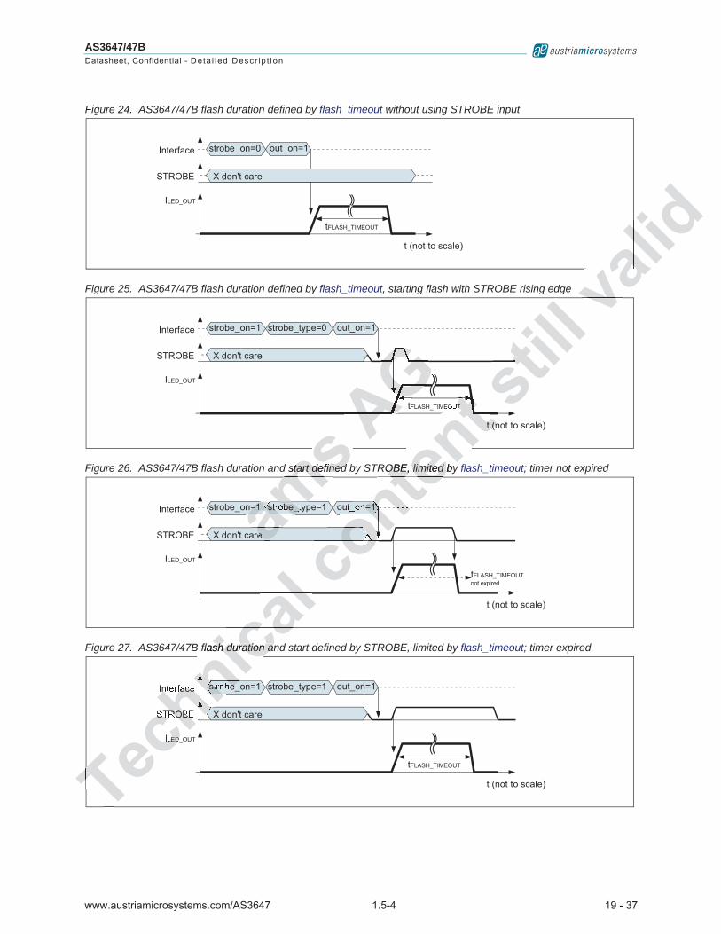
Flash Strobe TimingsThe flash timing are defined as follows:
1. Flash duration defined by register flash_timeout and flash is started immediately when this mode is selected by the I2C command (see Figure 24):set strobe_on = 0, start the flash by setting out_on = 1
2. Flash duration defined by register flash_timeout and flash started with a rising edge on pin STROBE (see Fig-ure 25): set strobe_on = 1 and strobe_type = 0
3. Flash start and timing defined by the pin STROBE; the flash duration is limited by the timeout timer defined by flash_timeout (see Figure 26 and Figure 34): set strobe_on = 1 and strobe_type = 1
#$%&'()%*+ #$%&
'()%*+
,-./0��������
���� ������ �
������� �
�����������������
�������� ����������������
����� ����!� � ������"���������� ��
� �� ����������
������������������ �������������"���"�� ���������
#��������������������$�%������� �
&��������
#������������������������������
������������� �� ��
#'�(������
#'�(
������
������������
���� ������ �
������� �
�����������������
�������� ����������������
����� ����!� � ������"���������� ��
� �� ����������
������������������ �������������"���"�� ���������
#��������������������$�%������� �
&��������
� ���������������������"������� ���"�� ������"��������������"�� �
ams
am#
aaaaamamamamammmmmaaaaaaaaaaamamamamammmaaaaaamamamamammmmmmamms���
���"������
A��AG mended to opeended to opwn in Figure 23Figure 23::
with short diagnoth short diagnoGGAGA
Technicr vin_low_v_runow_v_run
e TimingsTimingsng are defined asg are defined a
ash duration defiduration defthe I22C commaC commaset set strobe_ostrobe_o
2. Flash du Flash dure 25ure 25set
3.
icall��
����� alal�!"
caco
nteont
connnnnntntntntntntntt
ooooonononononnnnnnononon����� ntenennnnntntntntntntntttnten
t ���� ���"��
tsh andh an tt sstil
diagnostic flash anostic flash a
ain-Flan-Flatill
tilss
alid
valial
www.austriamicrosystems.com/AS3647 1.5-4 19 - 37
AS3647/47BDatasheet, Confidential - Deta i led Descr ip t ion
Figure 24. AS3647/47B flash duration defined by flash_timeout without using STROBE input
Figure 25. AS3647/47B flash duration defined by flash_timeout, starting flash with STROBE rising edge
Figure 26. AS3647/47B flash duration and start defined by STROBE, limited by flash_timeout; timer not expired
Figure 27. AS3647/47B flash duration and start defined by STROBE, limited by flash_timeout; timer expired
+����+�+�����,�
� ������
������
���� �
�������������
��������� �������
����� �� �
�!������� "#
���$����
������
�����������
� ��������� �� ������ ����� �����
������ �����
�� ������
���� � ����� �!
�"#���
��$%
�"���������
�� ��'�����
��������� � �����
������������
��������������������
����������������
�������
�!�"�
���# $��%����
��&������� �������
����������
��� ���������������
msstart defined start defineds sam
saa��aa�amam�������� ms AG
AAGGAGGAGAGGGG
Technicaflash duration ash duration anca
l alca
Technichhhnhnhnhn
����
hnh������hhnhn�� �hh� ���
TTnic
tenROBE, limited byOBE, limited bent t����ttt�
en
contennnnnnnoonon��
con
conooonte
still
stva
lide va
livaa
lvv
www.austriamicrosystems.com/AS3647 1.5-4 20 - 37
AS3647/47BDatasheet, Confidential - Deta i led Descr ip t ion
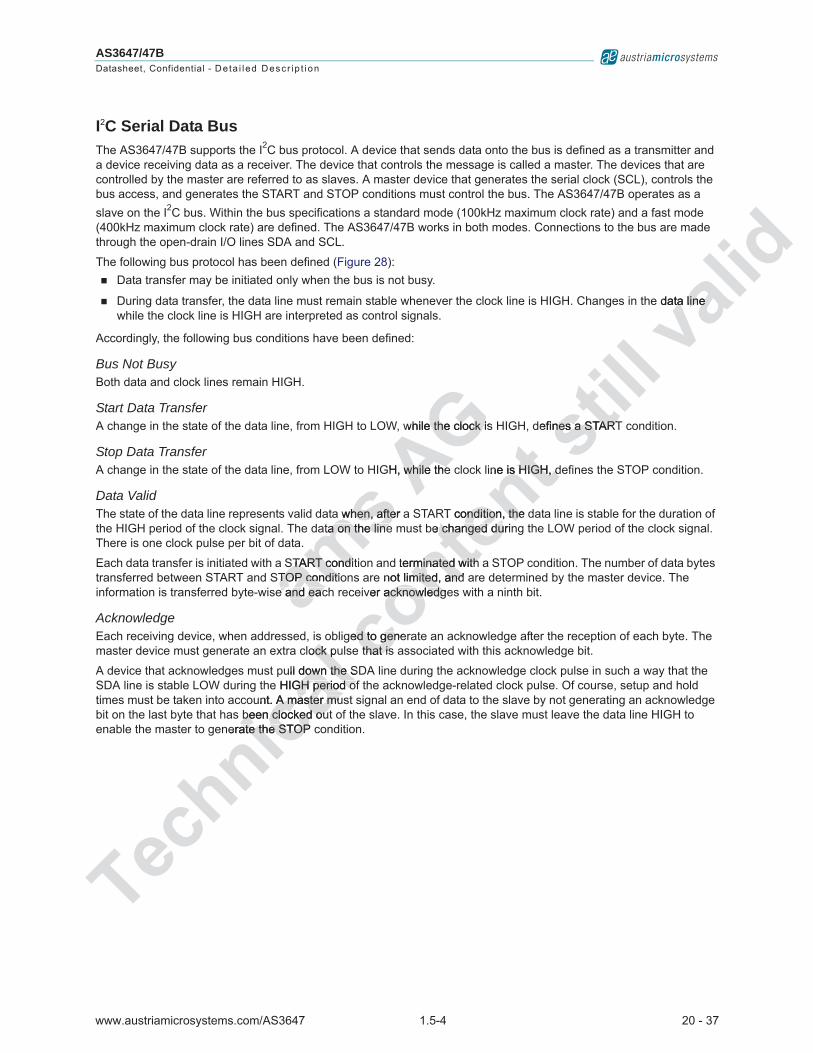
I2C Serial Data BusThe AS3647/47B supports the I2C bus protocol. A device that sends data onto the bus is defined as a transmitter and a device receiving data as a receiver. The device that controls the message is called a master. The devices that are controlled by the master are referred to as slaves. A master device that generates the serial clock (SCL), controls the bus access, and generates the START and STOP conditions must control the bus. The AS3647/47B operates as a slave on the I2C bus. Within the bus specifications a standard mode (100kHz maximum clock rate) and a fast mode (400kHz maximum clock rate) are defined. The AS3647/47B works in both modes. Connections to the bus are made through the open-drain I/O lines SDA and SCL.
The following bus protocol has been defined (Figure 28):Data transfer may be initiated only when the bus is not busy.
During data transfer, the data line must remain stable whenever the clock line is HIGH. Changes in the data line while the clock line is HIGH are interpreted as control signals.
Accordingly, the following bus conditions have been defined:
Bus Not BusyBoth data and clock lines remain HIGH.
Start Data TransferA change in the state of the data line, from HIGH to LOW, while the clock is HIGH, defines a START condition.
Stop Data TransferA change in the state of the data line, from LOW to HIGH, while the clock line is HIGH, defines the STOP condition.
Data ValidThe state of the data line represents valid data when, after a START condition, the data line is stable for the duration of the HIGH period of the clock signal. The data on the line must be changed during the LOW period of the clock signal. There is one clock pulse per bit of data.
Each data transfer is initiated with a START condition and terminated with a STOP condition. The number of data bytes transferred between START and STOP conditions are not limited, and are determined by the master device. The information is transferred byte-wise and each receiver acknowledges with a ninth bit.
AcknowledgeEach receiving device, when addressed, is obliged to generate an acknowledge after the reception of each byte. The master device must generate an extra clock pulse that is associated with this acknowledge bit.
A device that acknowledges must pull down the SDA line during the acknowledge clock pulse in such a way that the SDA line is stable LOW during the HIGH period of the acknowledge-related clock pulse. Of course, setup and hold times must be taken into account. A master must signal an end of data to the slave by not generating an acknowledge bit on the last byte that has been clocked out of the slave. In this case, the slave must leave the data line HIGH to enable the master to generate the STOP condition.
amsa when, after when, afte
ata on the linea on the line
START conditSTART conditSTOP conditioTOP condite and eace and eac
AG while the clock is e the clock i
GH, while thewhile the
Technica
l s
clock puock p
ull down the SDown the Se HIGH period ofGH period o
unt. A master muA master mubeen clocked oubeen clocked ou
nerate the STOP ate the STOP
conten
t ine is HIGH, dis HIGH, d
T condition, the dondition, thebe changed durine changed du
terminated with minated with not limited, and mited, and
ver acknowledgeacknowledg
ged to geneed to genthat isthat is
still
efines a STARTnes a START
valide data line ta line
www.austriamicrosystems.com/AS3647 1.5-4 21 - 37
AS3647/47BDatasheet, Confidential - Deta i led Descr ip t ion
Figure 28. Data Transfer on I2C Serial Bus
Depending upon the state of the R/W bit, two types of data transfer are possible:
1. Data transfer from a master transmitter to a slave receiver. The first byte transmitted by the master is the slave address. Next follows a number of data bytes. The slave returns an acknowledge bit after each received byte. Data is transferred with the most significant bit (MSB) first.
2. Data transfer from a slave transmitter to a master receiver. The master transmits the first byte (the slave address). The slave then returns an acknowledge bit, followed by the slave transmitting a number of data bytes. The master returns an acknowledge bit after all received bytes other than the last byte. At the end of the last received byte, a “not acknowledge” is returned. The master device generates all of the serial clock pulses and the START and STOP conditions. A transfer is ended with a STOP condition or with a repeated START condition. Since a repeated START condition is also the beginning of the next serial transfer, the bus is not released. Data is transferred with the most significant bit (MSB) first.
The AS3647/47B can operate in the following two modes:
1. Slave Receiver Mode (Write Mode): Serial data and clock are received through SDA and SCL. After each byte is received an acknowledge bit is transmitted. START and STOP conditions are recognized as the begin-ning and end of a serial transfer. Address recognition is performed by hardware after reception of the slave address and direction bit (see Figure 29). The slave address byte is the first byte received after the master generates the START condition. The slave address byte contains the 7-bit AS3647/47B address, which is
0110000, followed by the direction bit (R/W), which, for a write, is 0.9 After receiving and decoding the slave address byte the device outputs an acknowledge on the SDA line. After the AS3647/47B acknowledges the slave address + write bit, the master transmits a register address to the AS3647/47B. This sets the register pointer on the AS3647/47B. The master may then transmit zero or more bytes of data, with the AS3647/47B acknowledging each byte received. The address pointer will increment after each data byte is transferred. The master generates a STOP condition to terminate the data write.
2. Slave Transmitter Mode (Read Mode): The first byte is received and handled as in the slave receiver mode. However, in this mode, the direction bit indicates that the transfer direction is reversed. Serial data is transmit-ted on SDA by the AS3647/47B while the serial clock is input on SCL. START and STOP conditions are recog-nized as the beginning and end of a serial transfer (Figure 30 and Figure 31). The slave address byte is the first byte received after the master generates a START condition. The slave address byte contains the 7-bit
AS3647/47B address, which is 0110000, followed by the direction bit (R/W), which, for a read, is 1.10 After receiving and decoding the slave address byte the device outputs an acknowledge on the SDA line. The AS3647/47B then begins to transmit data starting with the register address pointed to by the register pointer. If
9. The address for writing to the AS3647/47B is 60h = 01100000b10.The address for read mode from the AS3647/47B is 61h = 01100001b
SLAVE ADDRESS
ACKNOWLEDGEMENT SIGNAL FROM
RECEIVER
ACKNOWLEDGEMENT SIGNAL FROM
RECEIVER
REPEATED IF MORE BYTES ARE
TRANSFERRED
STOP CONDITIONOR REPEATED
START CONDITION
START CONDITION
SCL
SDA
MSB
R/WDIRECTION
BIT
ACK
1 2 6 7 8 9 1 2 3-7 8 9
ams ata byata
significant bgnificanttter to a mastter to a ma
an acknowledan acknowledcknowledge bcknowledge b
knowledge” isknowledge” isP conditions. conditions.d START d START
withwith
AGf data transfer areta transfer a
slave receve res. TheThAG GGGGGGAG
Technica
lode):odedge bit is trbit is
nsfer. Address er. Address(see Figure 29)Figure 29)
T condition. The sndition. The s
d by the directionby the directiohe device outputsevice outputs
ss + write bit, thewrite bit, thn the AS3647/47AS3647/47
wledging each bywledging each bster generates a generates a
Slave Transmittee TransmitHowever, in thever, in ted on SDAted on SDAnized as nized afirst byfirst by
ASA
conten
tble:e:
he first byte tranirst byte trareturns an acknorns an ackno
first.eiver. eiver. The mastThe mast
followed by the sowed by the all recereceived byteived byte
ed. The The master dmaster dfer is ended with ended with
on is also the bes also the beost significant bitsignificant b
two modes:o modes:
rial datarial datamit
stilltilllllllllll
STOP CONDSTOP CONOR REPOR REP
START CSTART Ctiltitiltitistva
lvavvva
lidal

www.austriamicrosystems.com/AS3647 1.5-4 22 - 37
AS3647/47BDatasheet, Confidential - Deta i led Descr ip t ion
the register pointer is not written to before the initiation of a read mode the first address that is read is the last one stored in the register pointer. The AS3647/47B must receive a “not acknowledge” to end a read.
Figure 29. Data Write - Slave Receiver Mode
Figure 30. Data Read (from Current Pointer Location) - Slave Transmitter Mode
Figure 31. Data Read (Write Pointer, Then Read) - Slave Receive and Transmit
S 0110000 0 A XXXXXXXX A A AXXXXXXXX XXXXXXXX AXXXXXXXX P
<Slave Address> <Word Address (n)> <Data(n)> <Data(n+1)> <Data(n+X)><RW
>
S - StartA - Acknowledge (ACK)P - Stop
Data Transferred(X + 1 Bytes + Acknowledge)
S 0110000 1 A XXXXXXXX A A AXXXXXXXX XXXXXXXX NAXXXXXXXX P
<Slave Address> <Data(n)> <Data(n+1)> <Data(n+X)><RW
>
S - StartA - Acknowledge (ACK)P - StopNA - Not Acknowledge (NACK)
Data Transferred(X + 1 Bytes + Acknowledge)
Note: Last data byte is followed by a NACK
<Data(n+2)>
S 0110000 0 A XXXXXXXX A 1 A0110000
<Slave Address><Word Address (n)>
<Data(n+2)>
<RW
>
S - StartSr - Repeated StartA - Acknowledge (ACK)P - StopNA - Not Acknowledge (NACK)
XXXXXXXX A A AXXXXXXXX XXXXXXXX NAXXXXXXXX P
<Data(n)> <Data(n+1)> <Data(n+X)>
Sr
<RW
>
Data Transferred(X + 1 Bytes + Acknowledge)
Note: Last data byte is followed by a NACK
amsmsmsmmmsA XXXXX
<Data(n+1)<Data(n+
AG lave Transmitter MTransmitterGAG
Technicahninihnhhn011000
RW
>W
>
ccc <<chchcccca
l ointer, Then ReadThen Readl
cca
TT
conten
t tententeten
(X +(Note: LaNote: L
<Data(n+2)>ta(n+2)>
t still tis
validal
www.austriamicrosystems.com/AS3647 1.5-4 23 - 37
AS3647/47BDatasheet, Confidential - Deta i led Descr ip t ion
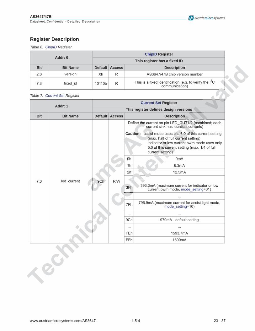
Register DescriptionTable 6. ChipID Register
Addr: 0ChipID Register
This register has a fixed ID
Bit Bit Name Default Access Description
2:0 version Xh R AS3647/47B chip version number
7:3 fixed_id 10110b R This is a fixed identification (e.g. to verify the I2C communication)
Table 7. Current Set Register
Addr: 1Current Set Register
This register defines design versions
Bit Bit Name Default Access Description
7:0 led_current 9Ch R/W
Define the current on pin LED_OUT1/2 (combined; each current sink has identical currents)
Caution: assist mode uses bits 6:0 of this current setting (max. half of full current setting)indicator or low current pwm mode uses only 5:0 of this current setting (max. 1/4 of full current setting)
0h 0mA
1h 6.3mA
2h 12.5mA
... ...
3Fh 393.3mA (maximum current for indicator or low current pwm mode, mode_setting=01)
... ...
7Fh 796.9mA (maximum current for assist light mode, mode_setting=10)
... ...
9Ch 979mA - default setting
... ...
FEh 1593.7mA
FFh 1600mA
ams
9Ch9Chamss AG e the cue the
currcu
Caution:on assist massist(m(m
AA
Technica
l ca
l
hn
cont
W.....
3Fh3Fh 3
..coonnteh ntenenn
t lf otor or lowr or lo
of this currentthis currencurrent setting)ent setting)nentent
oncoc
still_OUT1/2 (combiOUT1/2 (comb
identical currentstical curren
es bits 6:0 of thbits 6:0 of thll current s current
urrenrren
ill lllltillva
lidvava
lalavav
www.austriamicrosystems.com/AS3647 1.5-4 24 - 37
AS3647/47BDatasheet, Confidential - Deta i led Descr ip t ion
Table 9. TXMask Register
Addr: 3TXMask Register
This register defines the TXMask settings and coil peak current
Bit Bit Name Default Access Description
1:0 ext_torch_on 00 R/W
Defines operating mode for input pin TXMASK/TORCH
00 pin has no effect
01txmask-mode; during flash if TXMASK/TORCH=1, the
LED current is set to flash_txmask_current - (see TXMASK on page 16)
10
external torch mode: if TXMASK/TORCH=1 and mode_setting=00, the AS3647/47B is set into external torch mode (LED current is defined by the 7LSB1 bits
of led_current )
11 don’t use
3:2 coil_peak 10 R/W
Defines the maximum coil current (parameter ILIMIT)
00 ILIMIT = 2.0A
01 ILIMIT = 2.5A
10 ILIMIT = 3.0A
11 ILIMIT = 3.5A
7:4 flash_txmask_current2 6h R/W
Define the current on pin LED_OUT1/2 in flash mode if ext_torch_on=01 and TXMASK/TORCH=1
0h 0mA
1h 100mA
2h 201mA
3h 301mA
4h 402mA
5h 502mA
6h 602mA - default
7h 703mA
8h 803mA
9h 904mA
Ah 1004mA
Bh 1104mA
Ch 1205mA
Dh 1305mA
Eh 1405mA
Fh 1506mA
1. The MSB bit of this register not used to protect the LED; therefore the maximum current = half the maximum flash current
2.
ams
amss ADefDeAG es
01
1010
1111AAGGGAGAGA
Tec1. The MSB bit1. The MSB biflash currflash Tec
hnical 6h6h
e
cal
Tec
cont
W
2hh
3h3h
4hh
5h5hcoonnteh
ntenentcurrent on pin LErent on pin LE
t_torch_onh_on=01 a01 ant IILIMtntententnon
coc
still rrent (parameter rent (parameter
MIT = 2.0A2.0A
ILIMITMIT = 2.5A = 2.5A
ITT = 3.0A = 3.0
lilltilstssva
lide e ee
=1 and nd nto external external
he 7LSB7LSB11 bits bits alalv
www.austriamicrosystems.com/AS3647 1.5-4 25 - 37
AS3647/47BDatasheet, Confidential - Deta i led Descr ip t ion
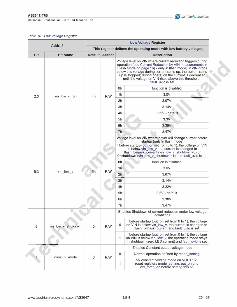
Table 10. Low Voltage Register
Addr: 4Low Voltage Register
This register defines the operating mode with low battery voltages
Bit Bit Name Default Access Description
2:0 vin_low_v_run 4h R/W
Voltage level on VIN where current reduction triggers during operation (see Current Reduction by VIN measurements in Flash Mode on page 16) - only in flash mode; if VIN drops below this voltage during current ramp up, the current ramp
up is stopped; during operation the current is decreased until the voltage on VIN rises above this threshold -
fault_uvlo is set
0h function is disabled
1h 3.0V
2h 3.07V
3h 3.14V
4h 3.22V - default
5h 3.3V
6h 3.38V
7h 3.47V
5:3 vin_low_v 5h R/W
Voltage level on VIN where driver will change current before startup (only in flash mode)
if before startup (out_on set from 0 to 1), the voltage on VIN is below vin_low_v, the current is changed to
flash_txmask_current (vin_low_v_shutdown=0) or 0=shutdown (vin_low_v_shutdown=1) and fault_uvlo is set
0h function is disabled
1h 3.0V
2h 3.07V
3h 3.14V
4h 3.22V
5h 3.3V - default
6h 3.38V
7h 3.47V
6 vin_low_v_shutdown 0 R/W
Enables Shutdown of current reduction under low voltage conditions
0if before startup (out_on set from 0 to 1), the voltage on VIN is below vin_low_v, the current is changed to
flash_txmask_current and fault_uvlo is set
1if before startup (out_on set from 0 to 1), the voltage on VIN is below vin_low_v, the operating mode stays in shutdown (zero LED current) and fault_uvlo is set
7 const_v_mode 0 R/W
Enables Constant output voltage mode
0 Normal operation defined by mode_setting
15V constant voltage mode on VOUT1/2;reset registers mode_setting, out_on and
ext_torch_on before setting this bit
5h5hams AVoltage leVoltag
beAAG7h7hAAGAG6h
AAGG GGGGAGA
Tec77Teechnica
n_low_v_shutdown_low_v_shutdow
e
cacal
cal
ca
ec
cont
/W1hh
2h2h
3h3hcoonnte0h nten
tVIN where drivN where drivstartup (only intartup (only i
artup (out_onout_on set sebelow ow vin_low_vvin_low
ash_txmask_currsh_txmask_curhutdown (tdown (vin_lowvin_lo
tttttent
oncoco
s.47V47Vst3.38V3.38Vsti3.3VV till- defaultdefault ill llilltistsva
lidd d -
alalvavv
www.austriamicrosystems.com/AS3647 1.5-4 26 - 37
AS3647/47BDatasheet, Confidential - Deta i led Descr ip t ion
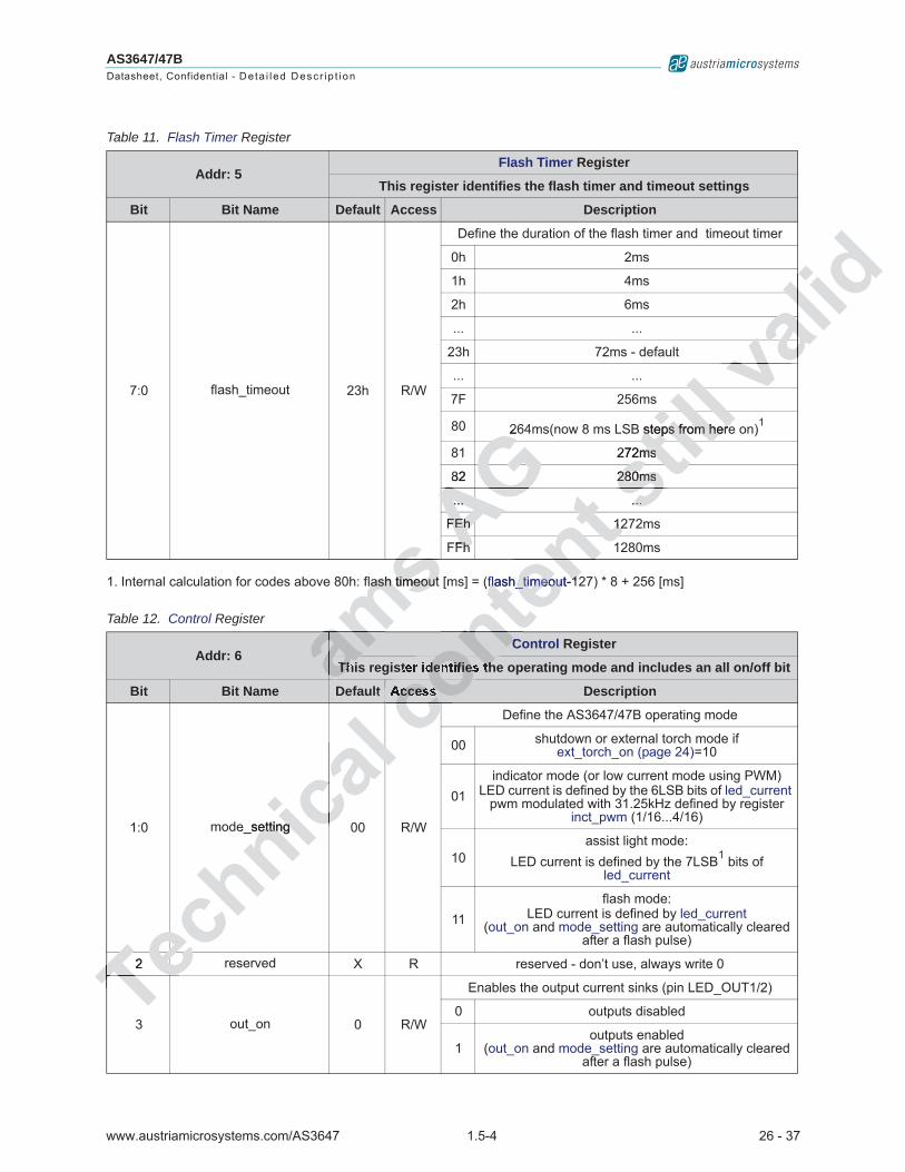
Table 11. Flash Timer Register
Addr: 5Flash Timer Register
This register identifies the flash timer and timeout settings
Bit Bit Name Default Access Description
7:0 flash_timeout 23h R/W
Define the duration of the flash timer and timeout timer
0h 2ms
1h 4ms
2h 6ms
... ...
23h 72ms - default
... ...
7F 256ms
80 264ms(now 8 ms LSB steps from here on)1
81 272ms
82 280ms
... ...
FEh 1272ms
FFh 1280ms
1. Internal calculation for codes above 80h: flash timeout [ms] = (flash_timeout-127) * 8 + 256 [ms]
Table 12. Control Register
Addr: 6Control Register
This register identifies the operating mode and includes an all on/off bit
Bit Bit Name Default Access Description
1:0 mode_setting 00 R/W
Define the AS3647/47B operating mode
00 shutdown or external torch mode if ext_torch_on (page 24)=10
01indicator mode (or low current mode using PWM)
LED current is defined by the 6LSB bits of led_current pwm modulated with 31.25kHz defined by register
inct_pwm (1/16...4/16)
10assist light mode:
LED current is defined by the 7LSB1 bits of led_current
11flash mode:
LED current is defined by led_current (out_on and mode_setting are automatically cleared
after a flash pulse)
2 reserved X R reserved - don’t use, always write 0
3 out_on 0 R/W
Enables the output current sinks (pin LED_OUT1/2)
0 outputs disabled
1outputs enabled
(out_on and mode_setting are automatically cleared after a flash pulse)
aaThaamams flash timeout lash timeoutss
aamaaAFhFhAAG......
FEhFEhAAGAG 82
AGGGG26
GGAGAA
Te2Teechnicae_settingetting
Technica
l
e
cal
TeTe
cocococoAccesscocondentifies thont
Cnten(flash_timeoutflash_timeou -121ent 1212ttnt
ennton
coco
s......st280ms280msstil
272msms till
B steps from heresteps from hereilllilltilstssva
lidallalvavav

www.austriamicrosystems.com/AS3647 1.5-4 27 - 37
AS3647/47BDatasheet, Confidential - Deta i led Descr ip t ion
1. The MSB bit of this register not used to protect the LED; therefore the maximum assist light current = half the maximum flash current
Table 13. Strobe Signalling Register
Addr: 7Strobe Signalling Register
This register defines the flash current reducing and mode for STROBE
Bit Bit Name Default Access Description
6 strobe_type 1 R/W
Defines if the STROBE input is edge or level sensitive; see also bit strobe_on (page 27)
0 STROBE input is edge sensitive
1 STROBE input is level sensitive
7 strobe_on 1 R/W
Enables the STROBE input
0 STROBE input disabled
1 STROBE input enabledin flash mode
Table 14. Fault Register
Addr: 8Fault Register
This register identifies all the different fault conditions and provide information about the LED detection
Bit Bit Name Default Access Description
0 fault_uvlo 0 R/sC1
an undervoltage event has happened - see Current Reduction by VIN measurements in Flash Mode on page 16
0 No
1 Yes
1 reserved 0 R reserved - don’t use
2 reserved 0 R reserved - don’t use
3 fault_txmask 0 R/sC1
TXMASK/TORCH event triggered during flash - see TXMASK event occurred on page 14
0 No
1 Yes
4 fault_timeout 0 R/sC1
see Flash Timeout on page 14
0 No fault
1 Flash timeout exceeded
5 fault_overtemp 0 R/sC1
see Overtemperature Protection on page 14
0 No fault
1 Junction temperature limit has been exceeded
6 fault_led_short 0 R/sC1
see Short Circuit Protection on page 14
0 No fault
1 A shorted LED is detected (pin LED_OUT1/2)
7 fault_ovp 0 R/sC1
see Overvoltage Protection on page 13
0 No fault
1 An overvoltage condition is detected (pin VOUT)
aaam00ams
ammsAccess
ms smssmsa
AentinfoAGAG GGAGA
Te66Teceechn
fault_ovefault_o
eehnicalt_timeoutmeout cacaca
l00
icalR
cal
icahn
ecT
cccocoRRcocon
coRcoonon11ontn00
oonntean undervoltage undervoltageeduction by VIN mon by VIN mtenen
tfferent faultout the LEDtgistetttentent
ononcoc
sstill nputnput
t disableddisabled
input enabledput enabledash modemode lltillsts
validle; see
ve
vee allalvav
www.austriamicrosystems.com/AS3647 1.5-4 28 - 37
AS3647/47BDatasheet, Confidential - Deta i led Descr ip t ion
1. R/sC = Read, self clear; after readout the register is automatically cleared
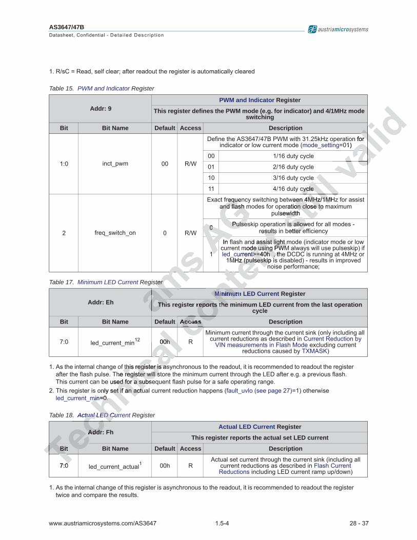
Table 15. PWM and Indicator Register
Addr: 9PWM and Indicator Register
This register defines the PWM mode (e.g. for indicator) and 4/1MHz mode switching
Bit Bit Name Default Access Description
1:0 inct_pwm 00 R/W
Define the AS3647/47B PWM with 31.25kHz operation for indicator or low current mode (mode_setting=01)
00 1/16 duty cycle
01 2/16 duty cycle
10 3/16 duty cycle
11 4/16 duty cycle
2 freq_switch_on 0 R/W
Exact frequency switching between 4MHz/1MHz for assistand flash modes for operation close to maximum
pulsewidth
0 Pulseskip operation is allowed for all modes -results in better efficiency
1
In flash and assist light mode (indicator mode or low current mode using PWM always will use pulseskip) if led_current>=40h , the DCDC is running at 4MHz or
1MHz (pulseskip is disabled) - results in improved noise performance;
Table 17. Minimum LED Current Register
Addr: EhMinimum LED Current Register
This register reports the minimum LED current from the last operation cycle
Bit Bit Name Default Access Description
7:0 led_current_min12 00h RMinimum current through the current sink (only including all
current reductions as described in Current Reduction by VIN measurements in Flash Mode excluding current
reductions caused by TXMASK)
1. As the internal change of this register is asynchronous to the readout, it is recommended to readout the register after the flash pulse. The register will store the minimum current through the LED after e.g. a previous flash. This current can be used for a subsequent flash pulse for a safe operating range.
2. This register is only set if an actual current reduction happens (fault_uvlo (see page 27)=1) otherwise led_current_min=0.
Table 18. Actual LED Current Register
Addr: FhActual LED Current Register
This register reports the actual set LED current
Bit Bit Name Default Access Description
7:0 led_current_actual1 00h RActual set current through the current sink (including all
current reductions as described in Flash Current Reductions including LED current ramp up/down)
1. As the internal change of this register is asynchronous to the readout, it is recommended to readout the register twice and compare the results.
aThaamams
sterter ms msmsaama
AGW00 PulsePulse
1
In cAAGAG requenrequand flash mand flash
AGA
T7:0TeTeBTech
Addrchnicathis register is asthis register is as
The register will stregister will sused for a subseed for a subs
only set if an actuset if an actuminmi =0.0.
Actual LED Curtual LED Cur
cal00h0h
cal
cal
ca
Tech
TeT
ccocoAccessconreports the ontMinimumnten
tnd assist light massist light mmode using PWMde using PWM
urrentt>=40h , th>=40h , tMHz (pulseskip iz (pulseskip i
ter
results sultstte
cont
oncoc
ston is allowen is allowbetter eetter esti
llween 4MHz/1MHzeen 4MHz/1MHeration close to mon close to
ulsewidthwidth ill cyclecycle llillstsva
lidlon for 01) allalvavv

www.austriamicrosystems.com/AS3647 1.5-4 29 - 37
AS3647/47BDatasheet, Confidential - Deta i led Descr ip t ion
Register Map
Table 21. Register Map 1
1. Always write’0’ to undefined register bits (e.g. to bits 4..7 of register 6)
Register Definition Addr Default Content
Name b7 b6 b5 b4 b3 b2 b1 b0
ChipID 0 Bxh fixed_id version
Current Set 1 9Ch led_current
TXMask 3 68h flash_txmask_current coil_peak ext_torch_on
Low Voltage 4 2Ch const_v_mode
vin_low_v_shutdown
vin_low_v vin_low_v_run
Flash Timer 5 23h flash_timeout
Control 6 00h out_on reserved mode_setting
Strobe Signalling 7 C0h strobe_on
strobe_type
Fault 8 00h fault_ovp
fault_led_short
fault_overtemp
fault_timeout
fault_txmask
reserved
reserved
fault_uvlo
PWM and Indicator 9 00h freq_swi
tch_on inct_pwm
Minimum LED Current Eh 00h led_current_min
Actual LED Current Fh 00h led_current_actual
amster bister bits (e.g.ts (e.ms smsmAGAGAGortort
fault_ovlt_overtempertemp
faultfaummAGG GGGGAGA
Technica
l conte4..7 of register 6of registerntenled_curreed_currten
tled_current_med_current_mnt nttm tnttennte
srest_txx reservereserddststi
ltiltillrvee
dd mode_mode_
tillltilstsva
lid_on
_v_runn allalvv

www.austriamicrosystems.com/AS3647 1.5-4 30 - 37
AS3647/47BDatasheet, Confidential - App l i ca t ion In fo rmat ion
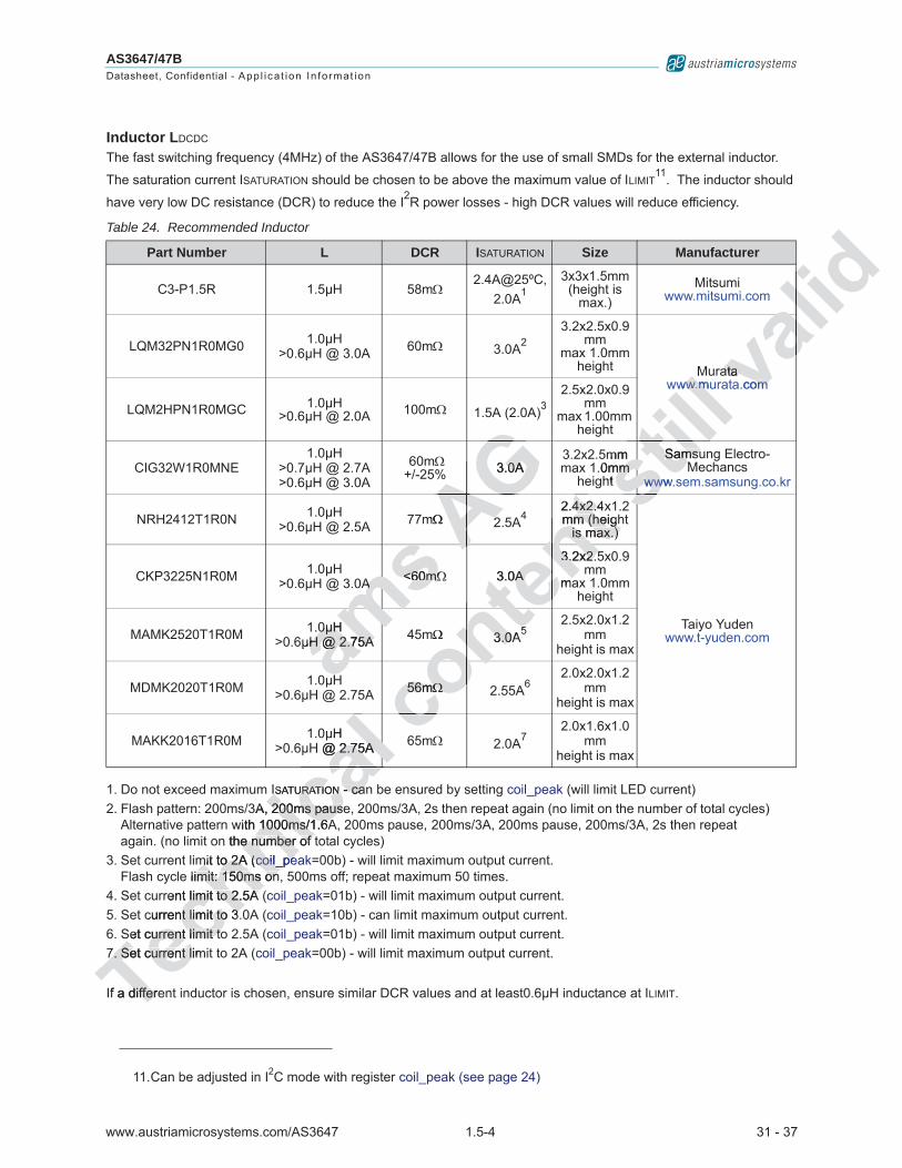
9 Application InformationExternal Components
Input Capacitor CVIN
Low ESR input capacitors reduce input switching noise and reduce the peak current drawn from the battery. Ceramic capacitors are required for input decoupling and should be located as close to the device as is practical.
If a different input capacitor is chosen, ensure similar ESR value and at least 3μF capacitance at the maximum input supply voltage. Larger capacitor values (C) may be used without limitations.
Add a smaller capacitor in parallel to the input pin VIN (e.g. Murata GRM155R61C104, >50nF @ 3V, 0402 size).
Output Capacitor CVOUT
Low ESR capacitors should be used to minimize VOUT ripple. Multi-layer ceramic capacitors are recommended since they have extremely low ESR and are available in small footprints. The capacitor should be located as close to the device as is practical.
X5R dielectric material is recommended due to their ability to maintain capacitance over wide voltage and temperature range.
If a different output capacitor is chosen, ensure similar ESR values and at least 4.2μF capacitance at 5V output volt-age.
Table 22. Recommended Input Capacitor
Part Number C TC Code Rated Voltage Size Manufacturer
GRM188R60J106ME4710μ
>3μ[email protected]>2μ[email protected]
X5R 6V3 0603 Muratawww.murata.com
LMK107BBJ106MA 10μ>3μ[email protected] X5R 6V3 0603 Taiyo Yuden
www.t-yuden.com
Table 23. Recommended Output Capacitor
Part Number C TC Code Rated Voltage Size Manufacturer
GRM219R61A116U 10μF +/-10%>4.2μF@5V X5R 10V 0805
Muratawww.murata.com
GRM188R60J106ME841
1. Use only for VLED < 3.75V
10μF +/-20%>4.2μF@4V X5R 6.3V
0603(1.6x0.8x0.85mm
max. 0.95mm height)
ams U
n small n sma
e to their abilto their abil
apacitorapacitoramCamaAG
e and at lee and at lhout limitationsut limitation
g. Murata GRM1g. Murata GRM1
ipple. Muple. tprpr
Technica
l capacitor is chosacitor is chos
@
75V5V
0μF +/-20%+/-20%>4.2μF@4V2μF@4Vlca
conten
tr ceramic capacramic capace capacitor shoupacitor sho
aintain capacitanntain capacita
cconC Code n
% X5RX5Rcnon
coc
still citance at the maxnce at the ma
4, >50nF @ 3>50nF @
Taiyo YudTaiyo Ywww.t-yuden.cwww.t-yudenlill
validalta
ata.coma.com allalv
www.austriamicrosystems.com/AS3647 1.5-4 31 - 37
AS3647/47BDatasheet, Confidential - App l i ca t ion In fo rmat ion
Inductor LDCDC
The fast switching frequency (4MHz) of the AS3647/47B allows for the use of small SMDs for the external inductor.
The saturation current ISATURATION should be chosen to be above the maximum value of ILIMIT11. The inductor should
have very low DC resistance (DCR) to reduce the I2R power losses - high DCR values will reduce efficiency.
If a different inductor is chosen, ensure similar DCR values and at least0.6μH inductance at ILIMIT.
11.Can be adjusted in I2C mode with register coil_peak (see page 24)
Table 24. Recommended Inductor
Part Number L DCR ISATURATION Size Manufacturer
C3-P1.5R 1.5μH 58m2.4A@25ºC,
2.0A1
1. Do not exceed maximum ISATURATION - can be ensured by setting coil_peak (will limit LED current)
3x3x1.5mm (height is
max.)Mitsumi
www.mitsumi.com
LQM32PN1R0MG0 1.0μH>0.6μH @ 3.0A 60m 3.0A2
2. Flash pattern: 200ms/3A, 200ms pause, 200ms/3A, 2s then repeat again (no limit on the number of total cycles)Alternative pattern with 1000ms/1.6A, 200ms pause, 200ms/3A, 200ms pause, 200ms/3A, 2s then repeat again. (no limit on the number of total cycles)
3.2x2.5x0.9mm
max 1.0mm height Murata
www.murata.com
LQM2HPN1R0MGC 1.0μH>0.6μH @ 2.0A 100m 1.5A (2.0A)3
3. Set current limit to 2A (coil_peak=00b) - will limit maximum output current.Flash cycle limit: 150ms on, 500ms off; repeat maximum 50 times.
2.5x2.0x0.9mm
max 1.00mm height
CIG32W1R0MNE1.0μH
>0.7μH @ 2.7A>0.6μH @ 3.0A
60m +/-25% 3.0A
3.2x2.5mmmax 1.0mm
height
Samsung Electro-Mechancs
www.sem.samsung.co.kr
NRH2412T1R0N 1.0μH>0.6μH @ 2.5A 77m 2.5A4
4. Set current limit to 2.5A (coil_peak=01b) - will limit maximum output current.
2.4x2.4x1.2mm (height
is max.)
Taiyo Yudenwww.t-yuden.com
CKP3225N1R0M 1.0μH>0.6μH @ 3.0A <60m 3.0A
3.2x2.5x0.9mm
max 1.0mm height
MAMK2520T1R0M 1.0μH>0.6μH @ 2.75A 45m 3.0A5
5. Set current limit to 3.0A (coil_peak=10b) - can limit maximum output current.
2.5x2.0x1.2mm
height is max
MDMK2020T1R0M 1.0μH>0.6μH @ 2.75A 56m 2.55A6
6. Set current limit to 2.5A (coil_peak=01b) - will limit maximum output current.
2.0x2.0x1.2mm
height is max
MAKK2016T1R0M 1.0μH>0.6μH @ 2.75A 65m 2.0A7
7. Set current limit to 2A (coil_peak=00b) - will limit maximum output current.
2.0x1.6x1.0mm
height is max
aμHam0μH0μHμH @ 2.75AH @ 2.75Amms 0AA <60m<60m
mssmaAAAG
m 22AGAG 3.0A0A
AGGGAGA
Technica
If a differediffer
SATURATIONURATION - can - ca3A, 200ms pause200ms paus
with 1000ms/1.6A1000ms/1.6An the e number of tnumber of
mit to 2A (mit to 2A (coil_pecoil_pee limit: 150ms onmit: 150ms on
rent limit to 2.5A limit to 2.5A current limit to 3.t limit to 3.
Set current limit toSet current limit to7. Set current lim7. Set current l
aal μH
H @ 2.75A@ 2.75Aalllaco
n56m56m onontem 3.0A3.0A5
onntent
3.0AA3.2x2.53.2x2.5
ma
n ennt 2.4x2.4x4x2.4
mm (heighmm (heighis max.)is max.)nttnt
nteon
c
ssstimm.0mm mm ht
SamsuSamsuM
www.wwsttill
Mww.muww.m
ttisva
lidm
ataataa.comom
alial
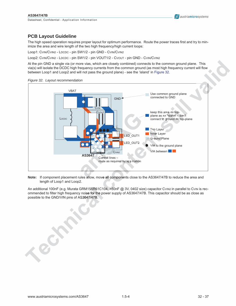
www.austriamicrosystems.com/AS3647 1.5-4 32 - 37
AS3647/47BDatasheet, Confidential - App l i ca t ion In fo rmat ion
PCB Layout GuidelineThe high speed operation requires proper layout for optimum performance. Route the power traces first and try to min-imize the area and wire length of the two high frequency/high current loops:
Loop1: CVIN/CVIN2 - LDCDC - pin SW1/2 - pin GND - CVIN/CVIN2
Loop2: CVIN/CVIN2 - LDCDC - pin SW1/2 - pin VOUT1/2 - CVOUT - pin GND - CVIN/CVIN2
At the pin GND a single via (or more vias, which are closely combined) connects to the common ground plane. This via(s) will isolate the DCDC high frequency currents from the common ground (as most high frequency current will flow between Loop1 and Loop2 and will not pass the ground plane) - see the ‘island’ in Figure 32.
Figure 32. Layout recommendation
Note: If component placement rules allow, move all components close to the AS3647/47B to reduce the area and length of Loop1 and Loop2.
An additional 100nF (e.g. Murata GRM155R61C104, >50nF @ 3V, 0402 size) capacitor CVIN2 in parallel to CVIN is rec-ommended to filter high frequency noise for the power supply of AS3647/47B. This capacitor should be as close as possible to the GND/VIN pins of AS3647/47B.
������������� ����������� �������
�����
����
�����
�������������� �����
����������
���� �����
������ ��
������ ��
�!��
���
��������"���#�����������$�"�� �� �����"���"�
%������"������������&����������'"��� '�#� �'������������� ������&����
�(
����)
�*�+���(
�*�+���)
AS3647
aallallamsmsssssmsmsmsmsms
��������msssmmmsmss ss�sssssss
a7
AGAAAAG AGAAAAAGAGAAAAAA�*�
Technica
l 55R6155R6oise for the por the
S3647/47B.47/47B.
con
ve all compoall componenne
04, >5004, >50
ontentntt
�� �
�
���� ��
���
��
� �����"���"�enenenenon
still
��
��������&'"��� '�#� �'�
��� ������
val
valid
valalal
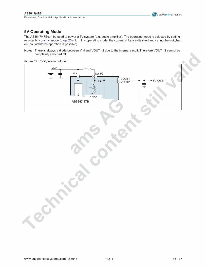
www.austriamicrosystems.com/AS3647 1.5-4 33 - 37
AS3647/47BDatasheet, Confidential - App l i ca t ion In fo rmat ion
5V Operating ModeThe AS3647/47Bcan be used to power a 5V system (e.g. audio amplifier). The operating mode is selected by setting register bit const_v_mode (page 25)=1. In this operating mode, the current sinks are disabled and cannot be switched on (no flash/torch operation is possible).
Note: There is always a diode between VIN and VOUT1/2 due to the internal circuit. Therefore VOUT1/2 cannot be completely switched off
Figure 33. 5V Operating Mode
���������������
� ��
��
�����
��
���
�
���
������
��� ��
����
���
����
��������
AS3647/47B
ams A
GAGGGAG AG
Technica
l conten
t sssstill
ss
valalid
alilal
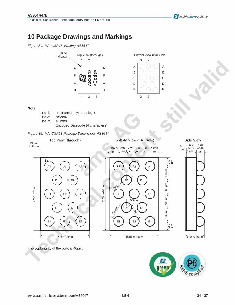
www.austriamicrosystems.com/AS3647 1.5-4 34 - 37
AS3647/47BDatasheet, Confidential - Package Drawings and Mark ings
10 Package Drawings and MarkingsFigure 34. WL-CSP13 Marking AS3647
Note:Line 1: austriamicrosystems logoLine 2: AS3647Line 3: <Code>
Encoded Datecode (4 characters)
Figure 35. WL-CSP13 Package Dimensions AS3647
The coplanarity of the balls is 40μm.
��������������� �� ������������ ������
� � �
��������� ���
�
�
�
�
� � �
�
�
�
�
���
�
�
�
�
���
�
�
�
�
� �A
S364
7<C
ode>
����������
�����
����
���
��� ��
��� ��
����
���
�
���
�
�����������������������
����������
��������
������������ �!"��
�����
���
#�$�%�&$��'���
���������
�������
�(�����
(������
)�)�)�
*�*�
+�+�+�
��
��
��
����
����
%�%�%�����
����
)�)�)�
*�*�
+�+�+�
����
%�%�%�
���
���
���
��
amsmmmssss���
amaaaaaaaaa�
AG A����
TecThe coplanarity oThe coplanarityechnica
l
hnica
ch������
aaaaiiiiccciciciciciihnhnhhhhhnnnnnnininnhnhnhnhnnnnnininiicicicc*
+�
t
conten
t
conte
c�
tnt n�
o
��������
coonnt
%� ntettentteteteete���eeenn��
still ll v
alid
vali
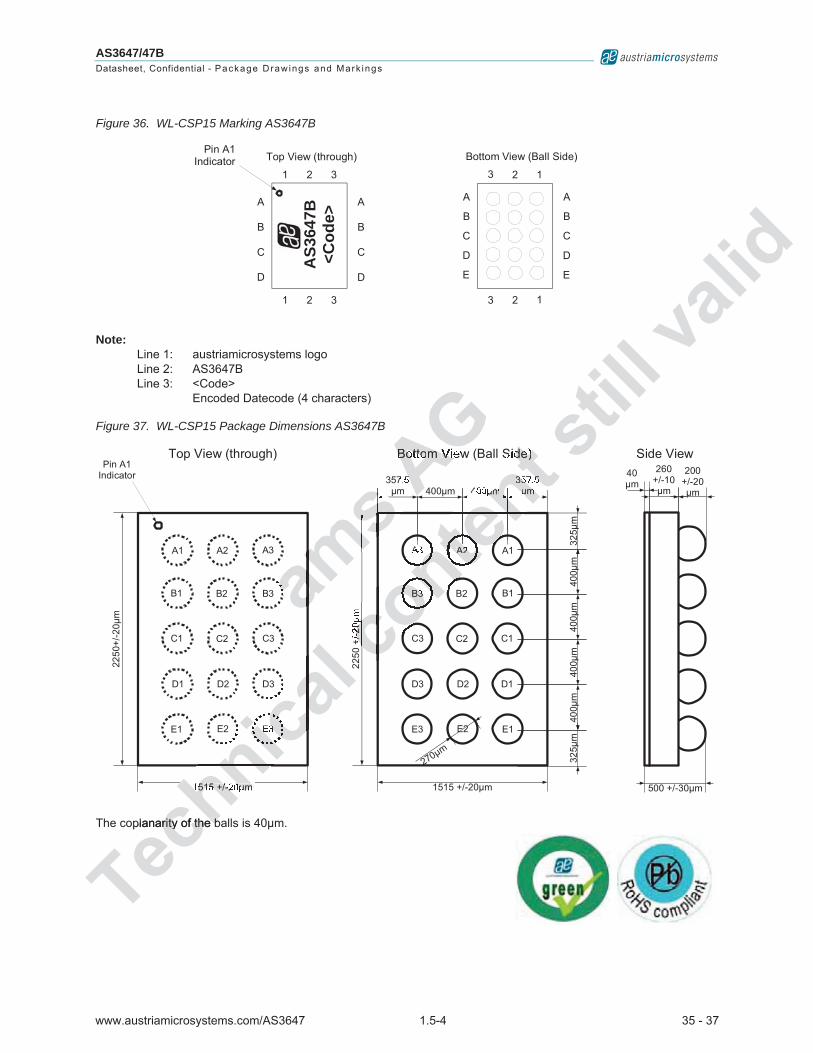
www.austriamicrosystems.com/AS3647 1.5-4 35 - 37
AS3647/47BDatasheet, Confidential - Package Drawings and Mark ings
Figure 36. WL-CSP15 Marking AS3647B
Note:Line 1: austriamicrosystems logoLine 2: AS3647BLine 3: <Code>
Encoded Datecode (4 characters)
Figure 37. WL-CSP15 Package Dimensions AS3647B
The coplanarity of the balls is 40μm.
������������ !�� ������������ ������
� � ,
��������� ���
�
�
�
�
� � ,
�
�
�
�
��,
�
�
�
�
��,
�
�
�
�
� �
AS3
647B
<Cod
e>
����������
�����
����
#������������ ������
������������
�����������
����������������
���������
���� �!���"����
��������
����������
�#��������
�������$���
%�%�%$
&�&�
'�'�'$
����
� � $
(����
(����
�$
&$
(����
(����
(����
$����
$����
(����$��)���
$��)���
%� %� %$
&� &�
'� '� '$
�� ��
� � $
�$
&$
(���
ams smsmss
amsss
aaaaAG AG����������A�
Techplanarity of the brity of the bchnica
l
hnicahn������������
'$ ccccnnnnnicnicniiiiiiiiccicicicicicicicicicco
ntent
conten
c������
���
nte �
nnte��
ntenco
nco
�$
ntennentt$��)�
��
still
sva
lidva
li
www.austriamicrosystems.com/AS3647 1.5-4 36 - 37
AS3647/47BDatasheet, Confidential - Order ing In fo rmat ion
11 Ordering InformationThe devices are available as the standard products shown in Table 25.
Note: All products are RoHS compliant and austriamicrosystems green.Buy our products or get free samples online at ICdirect: http://www.austriamicrosystems.com/ICdirect
Technical support is found at http://www.austriamicrosystems.com/Technical-SupportFor further information and requests, please contact us mailto:[email protected] find your local distributor at http://www.austriamicrosystems.com/distributor
Note: AS3647/47B-ZWLT
AS3647/47B-Z Temperature Range: -30ºC - 85ºCWL Package: Wafer Level Chip Scale Package (WL-CSP) 2.25x1.5x0.6mmT Delivery Form: Tape & Reel
Table 25. Ordering Information
Model Description Delivery Form Package
AS3647-ZWLT 1600mA High Current LED Flash Driver Tape & Reel
13-pin WL-CSP(2.25x1.5x0.6mm)
0.5mm pitchRoHS compliant / Pb-Free /
Green
AS3647B-ZWLT1
1. Check with austriamicrosystems for availability and lead time of AS3647B. AS3647B is only available upon request.
1600mA High Current LED Flash Driver Tape & Reel
15-pin WL-CSP(2.25x1.5x0.5mm)
0.4mm pitchRoHS compliant / Pb-Free /
Green
ams ustriaust
ge: -30ºC - 8e: -30ºC - 8evel Chipevel Chip
& R& R
AG ystems green.ms green.direct: dir http://wwwhttp://www
amicrosystems.crosystemstact us ct us ma
crosyros
Technica
l conten
technical-Snicales@austriamicr@austriamic
.com/distributorm/distributo
Package (WL-CSkage (WL-C
still
crosystems.cosystems
portt
ly available upoy available upolpGreG
ll valCSP
0.5mm)mmvalidee / e /
m pitchnt / Pb-Free /t / Pb-Fre alialv

www.austriamicrosystems.com/AS3647 1.5-4 37 - 37
AS3647/47BDatasheet, Confidential - Order ing In fo rmat ion
CopyrightsCopyright © 1997-2012, austriamicrosystems AG, Schloss Premstaetten, 8141 Unterpremstaetten, Austria-Europe.
Trademarks Registered ®. All rights reserved. The material herein may not be reproduced, adapted, merged, trans-
lated, stored, or used without the prior written consent of the copyright owner.
All products and companies mentioned are trademarks or registered trademarks of their respective companies.
DisclaimerDevices sold by austriamicrosystems AG are covered by the warranty and patent indemnification provisions appearing
in its Term of Sale. austriamicrosystems AG makes no warranty, express, statutory, implied, or by description regarding
the information set forth herein or regarding the freedom of the described devices from patent infringement. austriami-
crosystems AG reserves the right to change specifications and prices at any time and without notice. Therefore, prior
to designing this product into a system, it is necessary to check with austriamicrosystems AG for current information.
This product is intended for use in normal commercial applications. Applications requiring extended temperature
range, unusual environmental requirements, or high reliability applications, such as military, medical life-support or life-
sustaining equipment are specifically not recommended without additional processing by austriamicrosystems AG for
each application. For shipments of less than 100 parts the manufacturing flow might show deviations from the standard
production flow, such as test flow or test location.
The information furnished here by austriamicrosystems AG is believed to be correct and accurate. However,
austriamicrosystems AG shall not be liable to recipient or any third party for any damages, including but not limited to
personal injury, property damage, loss of profits, loss of use, interruption of business or indirect, special, incidental or
consequential damages, of any kind, in connection with or arising out of the furnishing, performance or use of the tech-
nical data herein. No obligation or liability to recipient or any third party shall arise or flow out of
austriamicrosystems AG rendering of technical or other services.
Contact InformationHeadquartersaustriamicrosystems AG
Tobelbaderstrasse 30
Schloss Premstaetten
A-8141 Austria
Tel: +43 (0) 3136 500 0
Fax: +43 (0) 3136 525 01
For Sales Offices, Distributors and Representatives, please visit:
http://www.austriamicrosystems.com/contact
amsn with o
pient or a
cal or other
AG addition
ufacturing flo
AG is believed
any third p
e, in
is
T
ica
Technica
l on
tems AG
trasse 30
Premstaette
8141 Austria
Tel: +43 (0) 31
x: +43
ical
iciccacaaico
ntent rrect
damag
business or i
e furnishing
y shall arise
still curren
ended tempe
medical life-sup
ustriamicrosys
deviations fr
accur
alid
valiaring
garding
ustriami-
refore, p
ati