august 16-17, 2021 held online
TRANSCRIPT

2021 EUVL Supplier Showcase
www.euvlitho.com 1
2021 EUVL Supplier Showcase
August 16-17, 2021
Held Online
Workshop Abstracts
2021 EUVL Supplier Showcase
www.euvlitho.com 2
Vivek Bakshi (EUV Litho, Inc.), Chair
Jinho Ahn (EUV-IUCC and Hanyang University), Co-Chair

2021 EUVL Supplier Showcase
www.euvlitho.com 3
Contents
Abstracts by Paper Numbers ________________________________________ 4

2021 EUVL Supplier Showcase
www.euvlitho.com 4
Abstracts
(Listed by Paper number)

2021 EUVL Supplier Showcase
www.euvlitho.com 5
SS1
Building a Success Company in EUVL - Growth of Energetiq Technology, Inc.
Debbie Gustafson
Wilmington, MA USA
www.energetiq.com
Energetiq Technology was founded in 2004 as a technology company developing 13.5nm
EUV light sources. Energetiq realized early that it would be critical for the success of the startup company to develop and sell product prior to EUV being in production. Energetiq
introduced a low power EUV metrology source in 2005. This source allowed critical infrastructure development of EUV Resist, Optics, Sensor and Mask inspection tools. To
date Energetiq has sold more than 40 EUV sources and as EUV has entered Semiconductor production the market is expanding. Debbie will share the success and struggles of Energetiq through the time from start up to present.
Presenting Author
Debbie Gustafson is the Chief Executive Officer of Energetiq Technology,
Inc. and a member of its board of directors. Ms. Gustafson joined the
company in 2005 as the VP of Sales, when the high technology start-up
introduced the first product. As CEO, Ms. Gustafson led the company into
a successful acquisition by Hamamatsu Corporation in 2017. She has
continued in her role as CEO as a wholly owned subsidiary of Hamamatsu
Corporation and is driving the integration and growth strategy.
Debbie has held strategic marketing and sales positions at Mykrolis
(Entegris), ASTeX (MKS), Teradyne and Helix (Brooks Automation). She
holds a BS in Mechanical Engineering from Southeastern Massachusetts
University (UMass Dartmouth) and an MBA in Management from Bentley
University. Currently Debbie is serving on the following boards; Energetiq
Technology; University of Massachusetts, Dartmouth College of
Engineering Advisory Council; SEMI Foundation, SEMI North American
Advisory Board; and SPIE Executive Advisory Council and Nominating
Committee.

2021 EUVL Supplier Showcase
www.euvlitho.com 6
SS2
Recent research activities in EUV-IUCC (Industry-University Collaboration Center)
Jinho Ahn
EUV-IUCC
http://www.euv-iucc.org/
EUV-IUCC (Industry-University Collaboration Center) is a non-profit organization supported by industry members. EUV-IUCC was organized in September 2019 to help member
companies to initiate their business in the field of EUV Lithography through providing information, education, networking and research collaboration. During the presentation, our recent research activities in the field of pellicle and mask in addition to the research
facilities will be briefly introduced.
Presenting Author
Jinho Ahn received his B.S. and M.S. degrees from Seoul National
University, and Ph.D. degree from the University of Texas at Austin all in
Materials Science and Engineering. He worked for Microelectronics
Research Laboratory at NEC, Tsukuba, Japan, and joined Hanyang
University in 1995 as a professor of Materials Science and Engineering. He
has been a leader of several national projects for advanced lithography.
He has authored over 200 technical papers and invented more than 50
patents. He worked as a Director of Nano and Convergence Technology at
National Research Foundation of Korea, the Vice President of Academic
Research, and the President of Industry-University Cooperation
Foundation at Hanyang University. He is now a Member of the National
Academy of Engineering of Korea, and a board member of National Nano
Infrastructure. He also works as a Director of EUV-IUCC since 2019. He
received the Semiconductor Technology Lifetime Achievement Award in
2015 from the President of Korea

2021 EUVL Supplier Showcase
www.euvlitho.com 7
SS3
Resist Technology for Single Digit Patterning: A solution for High-volume & High-throughput EUVL
Mohamad G. Moinuddin a, Satinder K. Sharma a,*, Kenneth E. Gonsalves b,**
Centre for Design & Fabrication of Electronic Devices, (C4DFED), SCEE a, SBS b,
Indian Institute of Technology (IIT)-Mandi, MANDI-175075, (Himachal Pradesh), India
www.c4dfed.iitmandi.ac.in; http://www.photoresistgroup.com
C4DFED@IIT Mandi, India is a unique class 100 cleanroom facility with sophisticated high-
end tools onsite to support multidisciplinary academic and industrial innovative research and prototyping in electronics and EUV resist technology. However, expensive EUV exposure technology is still scarce and out of reach from the resist developers. Hence, the
leading NGL pattering alternatives technologies: helium ion (He+) beam lithography (HIBL), electron beam lithography (EBL), along with imaging, deposition, etching, metrology
techniques including HR-FESEM, AFM, ALD, profilometry, contact lithography, maskless lithography, ellipsometer, stylus, sputtering, evaporation, etc. state-of-the-art facility has
been developed in-house to screening the developed NGL resists formulations prelude to EUVL high-volume chip manufacturing. What’s more, all relevant major resist formulation and materials characterization tools are available at the Photoresist Research Group facility
(PRG) and Advanced Materials Research Center (AMRC) at IIT Mandi.
EUVL is currently on the verge of high-volume production since the experimental load has been distributed, and the cost/exposure has been reduced since 2018. The semiconductor
roadmap suggests the primary concern is the downscaling of technology nodes, so the answer lies in the availability of compatible resist technology. Here @C4DFED, we
investigate the resist formulation reliability for single-digit (<10 nm) pattern generation and continuous improvement in the key metric needed for EUV insertion to the HVM. Since the limited EUV source availability, we prelude to the analogs SOPs (protocols) based on
readily available patterning and metrology screening tools and proven that developed resists have high sensitivity, lower LER/LWR, high etch resistance for EUVL applications.[1]
Beyond the general overview of the facility, we will focus on a few resist technologies developed in-house and subsequent competency of NGL pattering technologies down to single-digit, successfully demonstrated accomplishments onto indigenously resist
formulations for next-generation technology nodes. [1] All-new nickel-based Metal Core Organic Cluster (MCOC) resist for N7+ node patterning; Satinder K. Sharma, et al., "," Proc. SPIE 11326, Advances in Patterning Materials and Processes XXXVII, 1132604 (2020)

2021 EUVL Supplier Showcase
www.euvlitho.com 8
Presenting Author
Satinder K. Sharma [Ass.Prof.] (SMIEEE, SPIE, IETE-Fellow) received the
Master of Science in Physics (ES) from Himachal Pradesh University,
Shimla, India, in 2002, and Ph.D. from Department of Electronic Science,
Kurukshetra University, Kurukshetra, India, in 2007. From 2007 to 2010,
he was a PDF at DST Unit on Nanosciences, CHE, IIT-Kanpur, India.
From 2010 to 2012, he worked as a faculty with the Electronics and
Microelectronics Division, IIIT-Allahabad, India. Since 2012, he has been
working as a faculty with the School of Computing and Electrical
Engineering, IIT-Mandi, India. 2015 he worked as Visiting Faculty,
Institute of Semiconductor Electronics, Stuttgart University, Germany. He
published ~ 95 plus publications in the international peer-review Journals
and ~65 plus invited talks and research presentations in
international/national conferences, also submitted six patents. His current
research interest includes; Nano/microelectronics technology, circuits and
systems, noble CMOS devices, nano/microfabrication, advanced
lithography technology, sensors, and self-assembly, etc.

2021 EUVL Supplier Showcase
www.euvlitho.com 9
SS4
PAL-EUV synchrotron construction progress and EUV infrastructure operation plan
Sangsul Lee
Pohang Accelerator Laboratory, POSTECH
http://pal.postech.ac.kr
Due to the technical challenges in the EUV manufacturing process, technical advances in materials such as blank mask, pellicle and photo resist are needed.
Securing EUV R&D infrastructure is also essential, EUV light and analytical infrastructure based on synchrotron can help develop EUV materials.
Construction of compact synchrotron and EUV R&D infrastructure dedicated to EUV Lithography is underway at PAL campus to overcome the shortage of EUV research infrastructures.
PAL is supporting basic research such as photoresist evaluation and is planning to support
optical characteristics evaluation of blank mask, patterned mask and pellicle at the new EUV synchrotron in the near future.
Through the showcase, we would like to share and discuss PAL's progress for EUV infrastructure construction, which will be operated separately from early 2023 from the
existing synchrotron facilities. Presenting Author
Sangsul Lee is the head of the PAL-EUV metrology and inspection at
Pohang Accelerator Laboratory, POSTECH. He is also the chief technology
officer of Xavisoptics, an X-ray solution and equipment company. He
received PhD in materials science and engineering from the Hanyang
University in 2012. He currently runs X-ray nanoscale imaging beamline
and EUV test beamline at PAL. His research interest is synchrotron based
nanoscale imaging such as EUV metrology, inspection and nanoscale
tomography.

2021 EUVL Supplier Showcase
www.euvlitho.com 10
SS5
Preparing For The Next Generation of EUV Lithography at the Center for X-ray Optics
Ryan Miyakawa
CXRO
http://cxro.lbl.gov
The Center for X-ray Optics (CXRO) at Berkeley Lab has been a leader in EUV research for
the past 25 years. Leveraging 13.5-nm EUV light from the Advanced Light Source synchrotron facility, CXRO is home to several EUV research tools that have provided
important research insights into EUV resists, masks, and coatings. The 0.5-NA MET5 is a projection lithography tool capable of printing feature sizes down to 8 nm half-pitch. A new
radiation chemistry program is deploying several techniques aimed at dissecting the role of primary photo-electrons and secondary electrons in EUV resists. The SHARP microscope has been outfitted with anamorphic zone plate lenses which can emulate the geometry of
next generation EUV scanners. And the reflectometer is calibrated to measure both multilayer reflectivity as well as scattering profiles for the purpose of understanding the 3D
effects of EUV masks as well as determining mask properties. In parallel with these tools, the CXRO wavefront sensing program is developing high-resolution wavefront sensors suitable for measuring aberrations at high NA. This paper presents an overview of these
programs and describes how they will address the primary challenges that face the EUV community as it moves to the next generation of EUV lithography.
Presenting Author
Dr. Ryan Miyakawa is a research scientist at the Center for X-ray Optics at
LBNL where he works on the Berkeley MET5 and the SHARP EUV
microscope. Ryan’s interests include optical design for lithography and
imaging, and high-NA wavefront sensing.

2021 EUVL Supplier Showcase
www.euvlitho.com 11
SS6
EUV Mask Technology: Ready for 5nm and beyond
Yusuke Suzuki, Yusuke Suzuki
Dai Nippon Printing Co., Ltd.
https://www.dnp.co.jp/eng/index.html
Extreme ultraviolet lithography (EUVL) is introducing for manufacturing of advanced
semiconductor devices in last year to re-accelerate “More Moore”.
EUVL for 7nm logic node process has begun at the starting point and is expected to spread to cutting-edge processes for 5nm node and beyond down to 2nm node or so.
One of key technologies of EUVL is photomask manufacturing technologies that requires higher resolution, more precise accuracy and better productivity. To get the solution, DNP
has installed a Multi-Beam Mask Writer (MBMW). The MBMW tool is equipped with 262-thousand programmable beams, a 120-Gbps data-path, and an air-bearing stage, with sub-nm precision.
With this system, DNP has developed the EUV mask process with the low-sensitivity and
high-resolution resist for EUV lithography capable of 5nm node processes and beyond. MBMW also proves that its writing strategy is useful for patterning the very complex features, such as the curvilinear patterns, with 1x nm resolution and reasonable
throughput. In this presentation, we will discuss MBMW and its process capability of EUV mask application, e.g. local CD uniformity, minimum resolution, image placement accuracy,
curvilinear patterns and other applications. Presenting Author
Yusuke Suzuki is a sales manager at DNP, associate vice president at
PDMC until 2019, and is currently in charge of DNP's EUV mask
business. He has realized the joint development of EUV masks with
imec, and is leading DNP's collaboration with EUV related equipment and
material manufacturers.

2021 EUVL Supplier Showcase
www.euvlitho.com 12
SS7
Automated EUV tools for HVM – Pellicle Mounter/Demounter, Pellicle & Pod Inspection Systems
Sung Won Choi
FINE SEMITECH CORP.(“FST”)
www.fstc.co.kr
Over the few decades, technologies for semiconductor have advanced the integration density in accordance with the Moore’s law. Also, massive improvements have been made for device miniaturization. Current leading chipmakers already started to adopt Extreme
Ultraviolet Lithography (EUVL) and have extended the use of EUV in their mass production. Supplementary innovations are required in tool automation and quality assurance for EUVL
mass production. Fine Semitech Corp. (FST) has been developing EUV infrastructure tools: EPMD (EUV Pellicle Mounter & Demounter), EPIS (EUV Pellicle Inspection System) and EPODIS (EUV POD Inspection System). These systems are currently commercially available
for customers. • EUV Pellicle Mounter and Demounter (EPMD): FST developed a fully automated EUV
Pellicle Mounter and Demounter, the second generation of the Mask Shop Tool (MST). Main function of EPMD is to automatically mount and demount EUV pellicles.
• EUV Pellicle Inspection System (EPIS): EPIS was developed to inspect defects on
EUV pellicle’s membrane and backside of the mask. These defects can seriously impact production yield rates and performances of devices during EUV lithography
process. As a result, the importance of EUV pellicle is constantly increasing for chipmakers.
EUV POD Inspection System (EPODIS): EPODIS was developed to inspect plating quality and defects on EUV Dual Pods. The EUV Dual Pod consist of an inner pod and an outer pod.
As the importance of the contamination control of EUV mask increases, the importance of inspection on the EUV Dual Pod also increases.

2021 EUVL Supplier Showcase
www.euvlitho.com 13
Presenting Author
Joined FST in 2020, Dr. Sungwon Choi is the chief technology officer
(CTO) and a research director for EUV lithography automation technology.
Sungwon Choi has had over 19 years of experience in semiconductor R&D
and mass production for lithography process development. He began his
career in advanced process development at Samsung Electronics in 2003.
He was the leading member of the lithography mass production for 10 nm
LSI device and also led 7 nm, 5 nm and 4 nm logic device development.
He also received several R&D awards during his career in Samsung
Electronics. Sungwon Choi holds a M.S. degree in Aero/Astronautics from
Stanford University and a Ph.D. in Mechanical Engineering from UCLA.

2021 EUVL Supplier Showcase
www.euvlitho.com 14
SS8
EUV interference lithography and metrology at PSI
Iacopo Mochi
Paul Scherrer Institute
https://www.psi.ch/en/lmn
The Laboratory for Micro and Nanotechnology at the Paul Scherrer institute is a Swiss excellence center for EUV research. It provides industrial and academic users with access to
the XIL-II beamline at the Swiss Light Source (SLS). The beamline is dedicated to EUV research for semiconductor manufacturing and is equipped with two end-stations that exploit the coherence properties of the beam to investigate new materials and to perform
advanced mask metrology without the necessity of complex and expensive EUV optical systems.
The EUV-Interference Lithography end station is a state-of-the-art system used to print periodic and semi-periodic nanostructures with a critical dimension of 8 nm. The EUV IL
exposure tool is in operation since 2004 and it is successfully used for the screening and development of advanced EUV resist candidates for current and future technology nodes.
The metrology end station is called RESCAN and it consists of a lensless EUV microscope dedicated to actinic pattern mask inspection. Although RESCAN was developed as a demonstration tool, it can perform inspection of small mask samples and is fully compatible
with EUV pellicles. RESCAN has been used to detect and characterize programmed phase and amplitude defects as small as 50 nm on complex logic patterns and to characterize the
transmission and scattering of EUV pellicles as well as their impact on mask imaging. In this talk, we will present the status of the EUV research program at PSI and the available
services and collaboration opportunities. Presenting Author
Dr. Iacopo Mochi started working on EUV mask inspection at Lawrence
Berkeley Laboratory in the Center for X-Ray optics. He operated the
SEMATECH AIT, an EUV microscope for mask review. He later worked on
the design and development of SHARP, an advanced EUV mask review
tool that is currently operating at the Advanced Light Source in Berkeley.
Subsequently, Dr. Mochi worked as an EUV mask R&D engineer at IMEC
on the topic of sub-resolution assist features. He is currently a staff
scientist at the Swiss Light Source, and he is responsible for the technical
development of RESCAN, a lensless actinic system for mask defect
inspection.

2021 EUVL Supplier Showcase
www.euvlitho.com 15
SS9
Synchrotron-radiation based EUV metrology at PTB
Michael Kolbe, Victor Soltwisch, Frank Scholze
Physikalisch-Technische Bundesanstalt (PTB)
https://www.ptb.de/cms/en/ptb/fachabteilungen/abt7/fb-71/ag-712.html
PTB is the German national metrology institute. It supports cooperation partners from industry and science with metrological capabilities and know-how within joint research
projects. PTB uses synchrotron radiation in the THz, IR, UV, EUV, VUV, and soft X-ray spectral ranges at the electron storage rings Metrology Light Source (MLS) and BESSY II for basic and applied metrological tasks. For more than 20 years, the EUV-Radiometry
group develops and provides metrology services for the characterization of optical components and radiation detectors as well as the measurement of optical material
properties in the spectral range from 1 nm to 40 nm. It is worldwide recognized as a well-established partner for EUV metrology. PTB uses its synchrotron radiation laboratories also
for lifetime investigations of optical components and radiation detectors. PTB offers services to determine the spectral responsivity of radiation detectors with traceability to a cryogenic radiometer as a primary detector standard in the full spectral range from UV to X-ray. The
EUV-Radiometry group uses two measurement stations at the storage rings BESSY II and MLS: an EUV reflectometer which can accommodate large optical components like collector
mirrors for EUV plasma sources, and an EUV Ellipso-Scatterometer for reticle-size samples supporting measurements of reflection and scattering under arbitrary polarization conditions. The EUV nanometrology group develops methods for the actinic characterization
for EUV optical components, e.g., the surface and interface roughness of multilayer mirrors can be characterized by resonant diffuse EUV scattering. It also investigates methods for
the characterization of nanostructured surfaces, e.g., on wafer, by EUV and soft X-ray scattering and fluorescence. Presenting Author
Michael Kolbe received his Ph.D. (focusing on X-ray based analysis) in
2002. Since 2003 he is a scientist at PTB focusing on Metrology with
synchrotron radiation. His research activities include X-ray spectrometry,
UV/VUV radiometry, and EUV radiometry. Based on these activities, he
accumulated expertise in employing analytical techniques in the UV to soft
X-ray spectral range. In 2020 he became head of PTB’s EUV radiometry
group.

2021 EUVL Supplier Showcase
www.euvlitho.com 16
SS10
TNO, R&D service provider for the EUV Semiconductor Industry
Norbert Koster
TNO, The Netherlands
https://www.tno.nl/en/focus-areas/industry/roadmaps/semiconductor-equipment/
TNO is an independent research institute partly funded by Dutch and European
governments to support the industry with innovation and new technologies. The majority of the projects for industrial applications are based on contract research and are company
confidential. TNO has been and still is in close cooperation with ASML and Carl Zeiss since the beginning of the EUV development in 2000. Much of the knowledge developed by TNO
is now being used for screening of materials and modules for EUV applications. TNO continues to invest in cooperation with the main players in EUV resulting in a strong background, knowledge, skills and facilities for the EUV community. TNO is capable of
performing EUV exposures and contamination experiments to understand the damage mechanisms occurring in among others EUV optics, masks, pellicles and new absorber
materials as well as realization of sensors and opto- mechatronic (sub)systems for equipment makers and realization of lab-tools. As independent organization TNO offers a high degree of reliability, flexibility, openness and transparency while respecting the
required secrecy of research results for individual customers.
Presenting Author
Norbert Koster is Principal Scientist at TNO in the group for Nano-
instrumentation, he has worked in vacuum technology and EUV
lithography since 1992. After graduation he worked at the former FOM
Institute for Plasma Physics Rijnhuizen. There he was involved in the
fabrication and optimization of Multilayer Mirrors for EUVL applications and
space astronomy as well as the improvement of the deposition tools. In
1999 he started at TNO as vacuum engineer. Together with ASML and
partners he stood at the birthplace of the EUV Alfa demo tools and their
successors. During his career he developed interest in vacuum
engineering, systems engineering and contamination control. As Principal
Scientist he is involved in projects for EUV Lithography, plasma
technology, contamination control, nuclear fusion (ITER).He was deeply
involved in the realization of a new EUV exposure facility (EBL2) for EUV
optics lifetime research at TNO in Delft.
2021 EUVL Supplier Showcase
www.euvlitho.com 17
SS11
Irradiation systems for accelerated testing of EUVL components
Jochen Vieker and Klaus Bergmann
Fraunhofer Institute for Laser Technology – ILT
https://www.ilt.fraunhofer.de/en.html
Fraunhofer ILT has been developing EUV sources for more than 2 decades. In collaboration with Philips and Ushio, ILT has contributed to the development of discharge based sources,
which have been operated in the first EUV lithography scanners for chip production. Having the know-how on EUV sources and their implementation into optical system at hand, ILT has been developing multitude of applications in collaboration with RWTH Aachen
University, e.g., EUV laboratory-scale lithography for patterning and resist testing with demonstrated resolution of 28 nm HP or EUV reflectometry for surface sensitive analysis.
The talk will focus on the Fraunhofer high Irradiance Tool (FIT) for testing of optical components. It is based on our proven FS5440 high power EUV source, whose emission is focused on a sample in controllable atmosphere. Using strong vacuum separation and
particle mitigation, an extremely low operating pressure at the irradiation position can be achieved without pumping orifices in the vicinity the focal spot. Thus, clean, unbiased
experimental conditions can be achieved. The expected performance of the FIT includes: EUV irradiance >40 W/cm², angle of incidence on sample <5°, spot diameter >1.8 mm and
pulse repetition rate up to 2.5 kHz. The design of the system allows multiplexing to reach 10 kHz and a higher power on sample. An updated design and new results based on optical and gas-flow simulations will be presented.
Presenting Author
Jochen Vieker received his Diplom (M. Sc. equiv.) in physics in 2011 from
Bielefeld University, for his work on high harmonic generation. Since then
he has been scientist in the EUV technology group at the Fraunhofer
Institute for Laser Technology and finished his PhD in physics in 2019 at
RWTH Aachen University for his research on power and lifetime scaling of
discharge based EUV sources. He is manager of the R&D projects and
architect of ILT’s EUV systems. Fields of interest include fundamental
research on EUV sources and secondary sources based on laser radiation
as well as their applications.

2021 EUVL Supplier Showcase
www.euvlitho.com 18
SS12
NIST at-wavelength EUVL metrology
C. Tarrio, R. E. Vest, R. F. Berg
NIST, Gaithersburg, MD, USA
https://www.nist.gov/
At the National Institute of Standards and Technology we have been involved in direct support of the developers of EUV Lithography for over 30 years. Our program began with characterization of EUV detectors and other optical elements. In the last couple of
decades, we have responded to the needs of the EUVL community by developing a more specialized suite of capabilities including accurate reflectometry of large mirrors,
contamination measurement and modeling, and out-of-band measurements. We will describe our capabilities and offer a few recent highlights Presenting Author

2021 EUVL Supplier Showcase
www.euvlitho.com 19
SS13
AtOMS - Combined Atomic Absorption /Optical Emission Spectroscopy for In-Situ Control of EUVL Thin Films
George Atanasoff
AccuStrata, Inc.
11900 Parklawn Drive, Rockville, MD 20852
https://www.accustrata.com/
The extremely thin metal-silicide and interface-engineered thin films, required for the EUVL
and X-ray mirrors, fall below the detection threshold of the traditional in-situ methods utilizing direct monitoring of the substrate. The in-situ control of deposition rate of opaque materials as well as the chemical composition of compound materials and alloys also
remain beyond the capability of the traditional in situ methods and require novel monitoring solutions.
AtOMS1 provides a practical solution for in situ deposition control of extremely thin films, compound thin films and complex multilayer structures with controlled interfaces as well as
metal alloys and opaque films. It combines the methods of element-specific atomic absorption with the broadband optical emission (OE) measured in the plasma zone
surrounding the deposited/etched substrate and provides unique monitoring capability that cannot be achieved by using any of these two techniques alone. It provides sensitive and accurate values for the momentary element concentration of the films, their rate of
deposition and process conditions. The deposition rates of up to 4 individual chemical elements are monitored simultaneously and up to 3 separate probe beams can be launched
for physical modeling of the film parameters and their uniformity over large wafers. Fiber-optics switching allows configurability and customization to fit any chamber geometry with little or without any retrofitting. The fiber optics components allow flexible installation with
options for fast installation and demo outside the chamber through UV viewports, or inside the deposition area for unprecedented sensitivity and accuracy. Physical modeling and
machine learning are used or modeling the deposition parameters2 such as deposition rate and composition and providing dynamic feedback control.
• Atomic concentration and deposition rates of 4 chemical elements simultaneously
• In situ control of interface and barriers layers with thickness <10Å • In situ control of chemical composition of compound semiconductors and alloys
• Deposition rate accuracy - element specific (Mo→±0.005Å/s, Si→±0.01Å/s) • Film composition accuracy ±0.05 atomic % (element and process specific)
• Feedback control of individual vapor sources, process drift and fault detection • Distributed monitoring over 300 mm wafers by 3 probe beams simultaneously • Agnostic to substrate shape, position and motion

2021 EUVL Supplier Showcase
www.euvlitho.com 20
AtOMS dramatically reduces the process tuning time, facilitates process scale up, and lowers product cost. Specification as well as system installation and results from deposition of Mo, Si, B, W, and other thin films and multilayers are presented.
1. G. Atanasoff, C. Metting and H.von Bredow, US patent 10,408,744, (2019); 2. G. Atanasoff, US patent 8,918.198, (2014); EP 2,389,459 (2014);
Presenting Author
George Atanasoff is a founder and president of AccuStrata, a technology
innovator in the field of in situ process control for advanced manufacturing
based on distributed spectroscopic sensors and predictive analytics
software. Dr. Atanasoff is a well-recognized professional in the Optical
Engineering field with a career as university professor in Physics and over
30-years of project and executive R&D management experience. In 2008
he funded AccuStrata as part of the University of Maryland in College Park
and steered the company into a successful commercial venture. George
has over 60 scientific publications in this film design, process and
metrology, multiple patents and numerous scientific presentations
worldwide. Dr. Atanasoff has been a principal investigator of many federal
programs for developing process control systems for solar, solid-state
lighting, EUVL and environmental application. He received his PhD in
Physics from University of Sofia in Bulgaria. George can be reached at

2021 EUVL Supplier Showcase
www.euvlitho.com 21
SS15
Multitrigger (MTR): An Irresistible Photoresist
Warren Montgomery1, Mark Shepherd1, David Ure1, Alex Robinson1, Alexandra
McClelland1, Carmen Popescu1 and Alan Brown1, Tom Lada2, John Roth2, Ed Jackson2, and Todd Smith3
1Irresistible Materials Ltd.
Langdon House, Swansea Waterfront, Swansea SA1 8QY,
United Kingdom (https://irresistiblematerials.com/)
2Nano-C
33 Southwest Park Westwood, MA 02090
(https://nano-c.com/)
3MERCK KGAA, Frankfurter Strasse 250
Darmstadt, 64293, Germany
(www.emdgroup.com)
At the EUVL Supplier Forum, in 2020, Irresistible Materials (IM) demonstrated the
capability of the MTR series of high performance EUV photoresist and spin on hardmask. Since then, IM has continued to develop new formulations as the march to high resolving,
high sensitivity and low LWR photoresists continues. Traditional chemically amplified resists (CAR) have continued to enable the initial insertion of EUV lithography. However, the CAR systems appear to have reached the limits of their capability. The industry is once again in
search of a new photoresist platform that can deliver against the latest lithography node requirements.
The IM technology is called “The Multi-Trigger concept (MTR)” and is characterized by a reaction that will only occur when multiple elements of the resist are initiated concurrently
and in close proximity to one another (spatially speaking). The multi-trigger material presented consists of a base molecule and a crosslinker, which represent the resist matrix,
together with a photoacid generator (PAG). Research is underway, continuously, to improve this resist, and is currently focused on improving resist opacity and crosslinking density. LER figures below 3 nm for lines and spaces patterned at 14 nm half pitch using the high
opacity MTR resist on the EUV-IL exposure tool at Paul Scherrer Institute (PSI) will be shown. The research activity has been collaborative.
We will present a very high-level review of recent results and demonstrate the flexibility of the MTR system. We will not discuss results of hard mask but are happy to update any
interested parties independently; as the development of that material also continues.

2021 EUVL Supplier Showcase
www.euvlitho.com 22
Presenting Author
Warren is currently working with Irresistible Materials in several roles. He
is doing account management, technical materials development,
commercialization and strategy. Formerly, as VP of Technical and
Consortia Program Development at CNSE (formally Albany Nanotech),
Warren led process development efforts associated with new photoresists
focused on EUV lithography. Prior to CNSE, Warren worked at Applied
Materials, LSI Logic, ASML, AZ Microelectronic and IBM in various
technical and leadership roles related to photoresist design, processing,
and lithography. During his extensive career in Lithography, Warren has
written over 50 technical and marketing publications and been awarded
30 US and European patents: primarily focused on lithography materials
and processes. Warren served as BACUS President and Conference Chair
and is, presently, a member of the EUVL Infrastructure Supplier Board.
He has a B.S. in Chemistry from Marist College, a B.S. Business
Administration from Mount St. Mary College, a graduate certificate in
Program Management from SUNY Empire State College and an MBA from
City University.

2021 EUVL Supplier Showcase
www.euvlitho.com 23
SS16
IR PiFM – Potential for EUV Metrology
Sung Park
Molecular Vista, 6840 Via Del Oro, Suite 110, San Jose, CA 95119
www.molecularvista.com
In this talk, we introduce a new nanoscale and non-destructive chemical imaging technique called infrared photo-induced force microscopy (IR PiFM) where the dipole-dipole force due to IR absorption by the sample is measured by an atomic force microscope (AFM) along
with the standard AFM topography [1]. This IR photo-induced force (PiF) between the AFM tip and the sample is strongly enhanced at the apex of the metal-coated tip due to the
antenna effect and leads to a routine spatial resolution that is better than 10 nm. By coupling a widely tunable IR laser source (~600 to >4000 cm-1), IR PiFM can acquire IR absorption spectrum of various organic and inorganic materials for identification of
molecular materials. In addition to local IR spectroscopy, chemical mapping based on characteristic vibrational band of materials can highlight different chemical components to
relate local chemistry to topography. Its characteristics, including single molecule sensitivity, spectral resolution (~2 cm-1), sub-10nm spatial resolution, excellent agreement between nanoscale PiF-IR and bulk FTIR spectra, and non-destructive nature, all point to its
potential as a metrology tool for EUV lithography. The capabilities of IR PiFM will be highlighted by presenting data on various material systems.
[1] Nowak, D., et al., “Nanoscale chemical imaging by photoinduced force microscopy,” Sci. Adv. 2 (2016), e1501571.
Presenting Author
Sung is the CEO of Molecular Vista, which he co-founded with Prof. Kumar
Wickramasinghe (UC Irvine, formerly of IBM) in 2011 to provide research
and industrial tools for rapid and nanoscale imaging with chemical
identification. Sung has over 25 years of experience of industrial R&D,
engineering, marketing and sales, and operations. In the scanning probe
field, he co-founded Park Scientific Instruments (PSI), which was one of
the first commercial companies to develop and sell scanning tunneling
microscopes (STM) and atomic force microscopes (AFM). Prior to founding
Park Scientific Instruments, he worked as a post-doc at IBM Watson
Research Center. Sung earned his Ph.D. in Applied Physics from Stanford
University and BA in Physics from Pomona College.

2021 EUVL Supplier Showcase
www.euvlitho.com 24
SS17
The art of fabricating high reflective multilayer coatings
Philipp Naujok, Torsten Feigl
optiX fab GmbH, Hans-Knoell-Strasse 6, 07745 Jena, Germany
www.optixfab.com
In this tutorial the authors will explain the basics of high reflective EUV multilayer coatings. What are the elementary ideas behind these special coatings? What are main issues one
has to deal with in order to fabricate high reflective coatings?
The talk will cover the most important aspects of EUV multilayer coatings like optical coating design, material choice and explain theoretical reflectivity limits. More important, a
detailed view on the fabrication, experimental issues and solutions to these problems will be presented.
In the second part the author will present optiX fab´s product portfolio and show some
examples of high reflective EUV multilayer coatings. These cover a broad spectral range from short wavelength soft x-ray applications up to mirrors in the VUV range.
Presenting Author
Philipp Naujok studied Physics at the Friedrich-Schiller-University in Jena,
Germany. He received his Master of Science degree in 2013. Right after
that he started to work on this Ph.D. thesis in the EUV group at
Fraunhofer IOF in Jena, Germany. There, he worked on the development
of new multilayer coatings for the next generation of EUVL at 6.x nm
under the topic: Structural and optical properties of Boron based
multilayer coatings for BEUV lithography. He received his Ph.D in 2017.
In July 2017 Philipp Naujok joined the team at optiX fab as a senior
scientist. This company was founded in 2012 to commercialize Fraunhofer
IOF’s EUV optics research and development activities. Located in Jena,
Germany, optiX fab designs, develops and fabricates EUV imaging,
illumination and collector optics and is supplying chipmakers, EUV tool
and source manufacturers as well as institutes, universities, synchrotron
beamlines and EUV research consortia worldwide.
At optiX fab Philipp Naujok is mainly responsible for the development and
characterization of novel multilayer coatings covering a broad spectral
range from short wavelength soft x-ray applications up to mirrors in the
VUV range.

2021 EUVL Supplier Showcase
www.euvlitho.com 25
SS18
Rigaku EUV optics and detector technology
Peter Oberta
Rigaku Innovative Technologies Europe s.r.o. Novodvorská 994, Praha 4, 142 21, Czech Republic
https://www.rigaku.com/
This commercial presentation is an overview of the EUV applicable optics and detectors RITE can offer. RITE was established in 2008 as a Rigaku Corporation R&D center in
Europe. One of the three RC research units worldwide. RITE is producing lens coupled and fiber coupled X-ray cameras. The lens coupled camera has the highest real spatial resolution on the market. Another core product is replicated optics, which is a rotationally
symmetric optics used as a collector (elliptical shape) or collimator (parabolic shape). Newly available is also Wolter shape optics. Various metallic single layer coatings, including
e.g. gold and ruthenium, are available.
Presenting Author
Peter Oberta made his PhD in physics in the field of X-ray optics. Has
working experience from the Swiss Light Source, where he was
responsible for optics beamline layout design. Since 2021 he is the
Managing Director at Rigaku Innovative Technologies Europe.

2021 EUVL Supplier Showcase
www.euvlitho.com 26
SS19
TEUS - high-brightness EUV LPP light source based on fast rotating target: product overview and specifications
Konstantin Koshelev1,2, Alexander Vinokhodov1, Oleg Yakushev1, Vladimir Ivanov1,2,
Vladimir Krivtsun1,2, Alexander Lash1, Mikhail Krivokorytov1,2, Vyacheslav Medvedev1,2, Vladimir Gubarev1,3, Denis Glushkov4, Samir Ellwi4, Eugene Gorsky5,
Alexey Kiselev5
1 EUV Labs, Troitsk, Moscow, Russia
2 Institute of Spectroscopy of the Russian Academy of Science (ISAN), Moscow,
Troitsk, Russia 3 MIPT, Dolgoprudny, Russia
4 ISTEQ, Eindhoven, The Netherlands 5 TRDC, Troitsk, Moscow, Russia
We present performance metrics for the commercially available TEUS product line. TEUS-S is a high-brightness EUV LPP light source based on a fast rotating liquid metal target with
EUV collection angle of 0.05sr. The TEUS-S100 and S400 models employing 100W and 400W of average laser power respectively have been characterized wi0th particular
attention to the collector optics lifetime. It is estimated that 10% mirror reflectivity degradation will occur after 2 years for the TEUS-S100 and after 0.5 year for the TEUS-S400 in 24/7operation mode.
The TEUS-S400 source provides more than 30 mW of in-band (±1%) EUV radiation after
the debris mitigation system. Presenting Author
2021 EUVL Supplier Showcase
www.euvlitho.com 27
SS20
Vacuum Processing Equipment for EUVL Optics - deposition, etching and cleaning
Marcel Demmler
scia Systems GmbH, Annaberger Str. 240, 09125 Chemnitz, Germany
www.scia-systems.com
scia Systems provides precise surface processing equipment based on advanced ion beam and plasma technologies. Especially for EUVL applications we designed equipment for processing of different sizes substrates, some up to three meter in diameter. We provide
systems for Mo/Si multilayer deposition, reactive ion beam etching and high-quality dry cleaning and qualification.
Presenting Author
Marcel Demmler graduated in Physical Engineering in 2007. After his
graduation, he had a position in the R&D team in a company specified in
ion beam and plasma process technologies. In 2011 he started working as
a Sales Director in that company. Marcel Demmler joined scia Systems as
Sales Director right from the beginning in 2013, coordinating scia
Systems’ worldwide sales activities.
2021 EUVL Supplier Showcase
www.euvlitho.com 28
SS21
Veeco Ion Beam Technology for EUV Photomask
Meng Lee
1 Terminal Drive, Plainview, New York 11803, USA
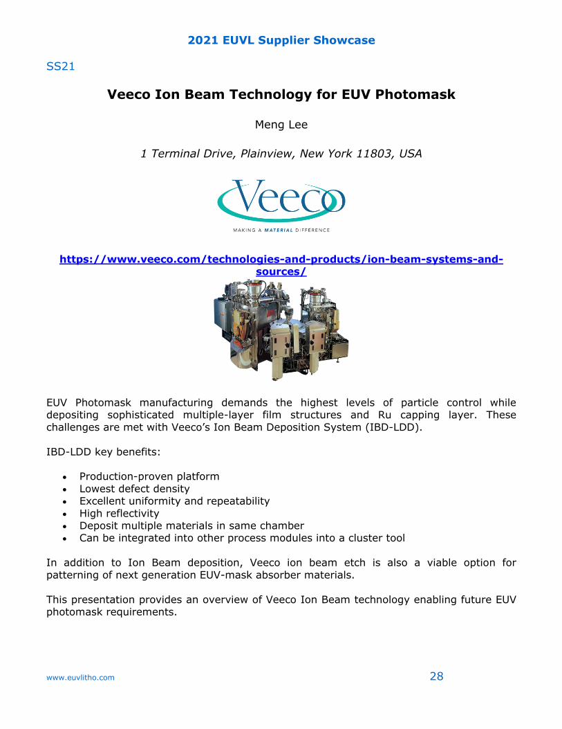
https://www.veeco.com/technologies-and-products/ion-beam-systems-and-sources/
EUV Photomask manufacturing demands the highest levels of particle control while depositing sophisticated multiple-layer film structures and Ru capping layer. These
challenges are met with Veeco’s Ion Beam Deposition System (IBD-LDD).
IBD-LDD key benefits:
• Production-proven platform
• Lowest defect density • Excellent uniformity and repeatability
• High reflectivity • Deposit multiple materials in same chamber • Can be integrated into other process modules into a cluster tool
In addition to Ion Beam deposition, Veeco ion beam etch is also a viable option for
patterning of next generation EUV-mask absorber materials.
This presentation provides an overview of Veeco Ion Beam technology enabling future EUV photomask requirements.
2021 EUVL Supplier Showcase
www.euvlitho.com 29
Presenting Author
Meng Lee, Director of Marketing at Veeco Instruments Inc.. He received
his Bachelor degree in Electrical and Electronics Engineering from
Louisiana State University in 1994 and his Master of Administration (MBA)
from California Lutheran University in 2005. He has more than 25 years
of experience in capital equipment business, driving strong technology
advancement to serve various markets including next generation ion
beam deposition and ion beam etch technology for EUV mask.

2021 EUVL Supplier Showcase
www.euvlitho.com 30
SS23
Product Differentiation in EUV Photomasks
Supriya Jaiswal
Astileux Corporation
https://astrileux.com
Presenting Author
Dr. Supriya Jaiswal is the CEO and Founder of Astrileux Corporation, a
next generation semi-conductor company. Astrileux designs advanced
engineering technologies that enable high volume manufacturing of next
generation integrated circuits (IC) chips at 7 nm and smaller that help
renew the promise of Moore’s law. Supriya holds a Bachelors degree in
Physics, from University of Oxford, UK, Masters degree in Atomic Physics
and a PhD in Engineering Physics from University of Virginia, and
professional qualifications in Business and Finance from University of
California, San Diego. In 2015 Supriya was elected to SPIE Senior Member
for distinction and honors in optics and photonics. She was the finalist
judge on the 2015 SPIE Photonics West Start-Up Challenge. She was
listed on SPIE’s 2016 Women in Optics. Astrileux is the first place winner
of the iMatSci Materials Research Society competition in 2016 and the
Semicon West Silicon Innovations forum in 2015, and the best start-up
award at the Electron, Ion and Photon Beam conference 2018. In 2019
Astrileux launched its first payload on the international space station and
was a finalist in 2019 World Materials Forum Prize. In 2019, she was
selected for the University of Oxford, Keble College most distinguished
alumni over the past 150 years.

2021 EUVL Supplier Showcase
www.euvlitho.com 31
SS24
Developments in KMLabs EUV Laser sources
Matt Harada and Henry C. Kapteyn
KMLabs
KMLabs has a 27-year history of leading photonics innovation. Most recently, we have developed the XUUSTM coherent EUV light source, a system for high-order harmonic
generation that represents a unique engineered, practical, commercial tabletop-scale x-ray/EUV laser source and beamline system. In contrast with plasma EUV sources, the XUUS
is a true coherent light source, capable of laser-like focusing to near the diffraction limit. The XUUS system can be paired with a variety of driving lasers, to generate light at 13.5 nm and longer EUV wavelengths for a variety of applications. Here, we highlight recent use
of the XUUS for interference lithography and coherent diffractive imaging relevant to nanoelectronics.
Presenting Author
Matt Harada is the President of KMLabs. Matt holds a BA in biology from
Brown University and an MBA from the University of Colorado at Boulder.
Prior to joining KMLabs, Matt served as the leader of several data and
software businesses.
Henry C. Kapteyn is co-founder and Chief Technology Officer of KMLabs.
Henry is well-established as a leading researcher in the area of ultrafast
optical science, and is Professor of Physics and a fellow of JILA, a joint
NIST/University institute at the University of Colorado at Boulder. He
received a BS from Harvey Mudd College, an MS from Princeton
University, and a Ph.D. in Physics from the University of California at
Berkeley in 1989. He has published more than 200 papers and won
multiple awards including the 2021 Benjamin Franklin Medal in Physics
