augmentation of a nano-satellite electronic power system
TRANSCRIPT

Augmentation of a Nano-Satellite Electronic Power System using a
Field-Programmable-Gate-Array
by
STEPHEN WILLIAM JOHN CUPIDO
Thesis is submitted in fulfilment of the requirements for the degree
Master of Technology: Electrical Engineering
in the Faculty of Engineering
at the Cape Peninsula University of Technology
Supervisor: Dr. M. Adonis
Co-supervisor: Mr. A. Barnard
Bellville
September 2013
CPUT copyright information The thesis may not be published either in part (in scholarly, scientific or technical journals) or as a whole
(as a monograph) unless permission has been obtained from the University.

ii
Declaration
I, Stephen William John Cupido, student number 204135192, declare that the contents of this
thesis represent my own unaided work, and that this thesis has not previously been submitted
for academic examination towards any qualification at any institution. Furthermore, it represents
my own opinions and not necessarily those of the Cape Peninsula University of Technology.
Signature Date
Bellville
September 2013

iii
Acknowledgments
I would like to acknowledge certain individuals as well as groups of people who in some way or
another contributed and encouraged me toward the completion of this thesis:
My supervisors, Dr. M. Adonis and Mr. A Barnard, for their continuous guidance and
support, as well as Mr. A. Raji for his input and ‘open door’ policy.
The CPUT and French South African Institute of Technology staff and students for their
assistance and support during the course of my endeavours.
God, with whom nothing is impossible, as well as my parents, family, friends, and in
particular my girlfriend Tatum Kroneberg, for believing in me and continuously motivating
me, especially towards the end of this journey.

iv
Abstract
The CubeSat standard has various engineering challenges due to its small size and surface
area. The challenge is to incorporate a large amount of technology into a form factor no bigger
than 10cm3. This research project investigates the space environment, solar cells, secondary
sources of power, and Field-Programmable-Gate-Array (FPGA) technology in order to address
the size, weight and power challenges presented by the CubeSat standard. As FPGAs have not
yet been utilised in this particular sub-system as the main controller, this research investigates
whether or not the implementation of an FPGA-based electronic power supply sub-system will
optimise its functionality by overcoming these size weight and power challenges.
The SmartFusion FPGA was chosen due to its analogue front end which can reduce the
number of peripheral components required by such complex systems. Various maximum power
point tracking algorithms were studied and it was determined that the perturb-and-observe
maximum power point tracking algorithm best suits the design constraints, as it only requires the
measurement of either solar cell voltage or solar cell current, thus further decreasing the
component count. The SmartFusion FPGA analogue compute engine allows for increased
performance of the perturb-and-observe algorithm implemented on the microcontroller sub-
system as it allows for the offloading of many repetitive calculations. A VHDL implementation of
the pulse-width-modulator was developed in order to produce the various changes in duty cycle
produced by the perturb-and-observe algorithm.
The aim of this research project was achieved through the development and testing of a nano-
satellite power system prototype using the SmartFusion FPGA from Microsemi with a decreased
number of peripheral circuits. Maximum power point was achieved in 347ms at worst case with
a 55% decrease in power consumption from the estimated 330mW as indicated in the power
budget. The SmartFusion FPGA consumes only a worst case of 148.93mW. It was found that
the unique features of the SmartFusion FPGA do in fact address the size weight and power
constraints of the CubeSat standard within this sub-system.
v
Contents
Declaration .................................................................................................................................. ii
Acknowledgments ...................................................................................................................... iii
Abstract...................................................................................................................................... iv
Contents ..................................................................................................................................... v
List of Figures ............................................................................................................................. x
List of Tables ........................................................................................................................... xiv
List of Abbreviations and Definitions ........................................................................................ xvi
Nomenclature ......................................................................................................................... xviii
Chapter 1 ................................................................................................................................... 1
Introduction ................................................................................................................................ 1
1.1 Background.................................................................................................................. 1
1.2 Problem Statement ...................................................................................................... 2
1.3 Objectives of the Research .......................................................................................... 2
1.4 Research Methodology ................................................................................................ 3
1.5 Delineation of the Research ......................................................................................... 3
1.6 Significance of the Research ....................................................................................... 4
1.7 Structure of the Thesis ................................................................................................. 4
Chapter 2 ................................................................................................................................... 5
Nano-Satellite Power Systems and the Environment in Space ................................................... 5
2.1 Nano-Satellite Power System Overview ....................................................................... 5

vi
2.2 Space Environment ...................................................................................................... 6
2.2.1 Orbital Parameters ................................................................................................ 6
2.3 Solar Cell Technology .................................................................................................. 8
2.3.1 Solar Cell Theory .................................................................................................. 9
2.3.2 Solar Cell Model ..................................................................................................11
2.3.3 Angle of Incidence ...............................................................................................14
2.4 Secondary Power Source ...........................................................................................16
2.4.1 Different Battery Technologies .............................................................................16
2.4.2 Li-ion Polymer Charging ......................................................................................18
2.5 Field-Programmable-Gate-Arrays (FPGAs).................................................................21
2.5.1 Microcontroller Sub-System (MSS) ......................................................................25
2.5.2 Analogue Front-End (AFE)...................................................................................25
2.5.3 Analogue Compute Engine (ACE) ........................................................................25
2.5.4 SmartFusion Power Usage ..................................................................................26
2.5.5 SmartFusion Power Calculation ...........................................................................27
2.6 Direct Energy Transfer (DET) .....................................................................................28
2.7 Maximum Power Point Tracking (MPPT) Algorithms ...................................................29
2.7.1 Perturb-and-Observe ...........................................................................................30
2.7.2 Incremental Conductance ....................................................................................30
2.7.3 Fractional Open Circuit Voltage ...........................................................................31
2.7.4 Fractional Short Circuit Current ............................................................................31
2.7.5 Neural Networks ..................................................................................................31
Chapter 3 ..................................................................................................................................33
Prototype Design and Simulation ..............................................................................................33
3.1 Overview of Design Solution .......................................................................................33
3.2 Orbital Parameters ......................................................................................................34

vii
3.3 Solar Cell Power Produced .........................................................................................36
3.4 Power Budget and Secondary Power Source Sizing ...................................................40
3.5 Perturb-and-Observe Maximum Power Point Tracking Algorithm ................................47
3.6 Distribution System and Load Switching .....................................................................50
3.6.1 5V Bus design ......................................................................................................50
3.6.2 3.3V Bus Design ..................................................................................................51
3.7 Active Load Design .....................................................................................................52
3.8 FPGA Functionality and Layout...................................................................................56
3.9 Matlab® Simulations ....................................................................................................60
Chapter 4 ..................................................................................................................................63
Prototype Construction ..............................................................................................................63
4.1 Circuit Level Design Overview ....................................................................................63
4.2 Solar Cell ....................................................................................................................64
4.3 Battery Charge/Discharge Circuit ................................................................................65
4.4 Distribution System .....................................................................................................69
4.5 Active Load .................................................................................................................71
4.6 FPGA ..........................................................................................................................72
4.6.1 Creating Design ...................................................................................................72
4.6.2 Implement Design ................................................................................................79
4.6.3 Programming Device ...........................................................................................82
4.6.4 Firmware Development ........................................................................................82
4.7 MPPT Circuit ...............................................................................................................83
Chapter 5 ..................................................................................................................................84
viii
Prototype Evaluation and Tests Results ....................................................................................84
5.1 Prototype Overview .....................................................................................................84
5.1.1 PWM Output Frequency ..........................................................................................86
5.1.2 Duty Cycle Verification ............................................................................................87
5.1.3 MPPT Verification ....................................................................................................89
5.1.4 Battery Charging Circuitry .......................................................................................91
5.1.5 Distribution System .................................................................................................92
5.2 System Integration ......................................................................................................94
5.2.1 Orbital Simulation Tests .......................................................................................96
Chapter 6 ................................................................................................................................ 102
Conclusion and Recommendations ......................................................................................... 102
6.1 Conclusion .................................................................................................................... 102
6.2 Problems Encountered .................................................................................................. 103
6.3 Recommendations for Future Work ............................................................................... 104
Publications emanating from the thesis ............................................................................... 105
References ............................................................................................................................. 106
Appendix A: Nano-Satellite Mission ........................................................................................ 111
Appendix B: MATLAB® Source Code ...................................................................................... 112
Appendix C: MATLAB® Source Code ...................................................................................... 113
Appendix D: MATLAB® Source Code ...................................................................................... 115
Appendix E: Power Budget ..................................................................................................... 117

ix
Appendix F: MPPT Circuit Design Calculations ....................................................................... 118
Appendix G: VHDL PWM ........................................................................................................ 122
Appendix H: VHDL PWM Test Bench ..................................................................................... 124
Appendix I: MATLAB® Binary Duty Cycle Calculations ........................................................... 127
Appendix J: Distribution System Circuit Design Calculations ................................................... 128
Appendix K: System Integration .............................................................................................. 131
x
List of Figures
Figure 2.1: Overview of a nano-satellite electronic power system (EPS) (Akagi, J. n.d) ............. 5
Figure 2.2: Irradiance affecting a satellite in orbit (Kjaer, 2002) .................................................. 8
Figure 2.3: Photoelectric effect (Horner, 2011) ........................................................................... 9
Figure 2.4: UTJ solar cell structure (Spectrolab, 2010) ..............................................................11
Figure 2.5: Solar cell model (Harjai et al., 2010) ........................................................................12
Figure 2.6: I-V characteristics at various levels of irradiance .....................................................12
Figure 2.7: P-V characteristics at various levels of irradiance ....................................................13
Figure 2.8: I-V characteristic curve and different operating temperatures ..................................14
Figure 2.9: P-V characteristic curves at different operating temperatures..................................14
Figure 2.10: Angle of incidence .................................................................................................15
Figure 2:11: Capacity loss versus percentage undercharged (Microchip, 2004)………………...18
Figure 2.12: Operating regions of Lithium-ion batteries (Microchip, 2004) .................................18
Figure 2.13: CC-CV charging profile (Dearborn, 2004) ..............................................................19
Figure 2.14: Loss in capacity at different charging voltages (Dearborn, 2004)...........................20
Figure 2.15: SmartFusion FPGA structure (Microsemi SoC Product Group, 2012) ...................24
Figure 2.16: Analogue compute engine partial block diagram (Actel Corporation, 2010) ...........26
Figure 2.17: SmartFusion power supply configuration (Microsemi SoC Product Group, 2012) ..28
Figure 2.18: Shunt regulated DET system without bus regulation (Bester, 2011) ......................29
Figure 2.19: Shunt regulated DET system with bus regulation (Bester, 2011) ...........................29
Figure 2.20: Maximum power point (Clark & Simon, 2007)........................................................30

xi
Figure 3.1: Proposed EPS design solution ................................................................................33
Figure 3.2: Solar cell area (Kjaer, 2002) ....................................................................................37
Figure 3.3: Solar cell layout .......................................................................................................38
Figure 3.4: 3-D rendition of proposed solar cell layout ...............................................................38
Figure 3.5: Perturb-and-observe MPPT algorithm .....................................................................48
Figure 3.6: MPPT implementation .............................................................................................49
Figure 3.7: Boost converter circuit .............................................................................................50
Figure 3.8: Boost converter output voltage and current .............................................................50
Figure 3.9: Buck converter circuit ..............................................................................................51
Figure 3.10: Buck converter output voltage ...............................................................................51
Figure 3.11: Buck converter output current ...............................................................................52
Figure 3.12: TIP 122 circuit diagram 3.3V bus ..........................................................................53
Figure 3.13: TIP 122 3.3V bus simulation results ......................................................................53
Figure 3.14: TIP 122 circuit diagram 5V bus .............................................................................54
Figure 3.15: TTP 122 5V bus simulation results ........................................................................54
Figure 3.16: SmartFusion eval-kit..............................................................................................57
Figure 3.17: Mixed signal daughter board .................................................................................58
Figure 3.18: Mixed signal connector ..........................................................................................59
Figure 3.19: Matlab simulation of MPPT implementation ...........................................................60
Figure 3.20: Solar cell model .....................................................................................................61
Figure 3.21: Solar cell characteristics ........................................................................................61
xii
Figure 3.22: MPPT output waveform .........................................................................................62
Figure 4.1: Basic circuit level design overview ..........................................................................63
Figure 4.2: Solar cell used in simulated environment ................................................................64
Figure 4.3: LTC4054-4.2 Lithium-ion battery charger ................................................................66
Figure 4.4: State of charge detection ........................................................................................67
Figure 4.5: Battery charge algorithm .........................................................................................68
Figure 4.6: Battery charge/discharge circuit ..............................................................................69
Figure 4.7: 3.3V buck converter prototype .................................................................................70
Figure 4.8: 5V boost converter prototype ..................................................................................70
Figure 4.9: Active load circuit ....................................................................................................71
Figure 4.10: Active load setup ...................................................................................................71
Figure 4.11: Smart design canvas .............................................................................................73
Figure 4.12: Clock configuration ................................................................................................73
Figure 4.13: ABPS internal configuration...................................................................................74
Figure 4.14: ACE configuration .................................................................................................75
Figure 4.15: Current monitor .....................................................................................................76
Figure 4.16: Sample Sequence Engine (SSE) configuration .....................................................76
Figure 4.17: GPIO configuration ................................................................................................77
Figure 4.18: MSS and VHDL PWM ...........................................................................................78
Figure 4.19: Test bench output .................................................................................................80
Figure 4.20: Application code flowchart .....................................................................................82

xiii
Figure 4.21: MPPT prototype ....................................................................................................83
Figure 5.1: Electronic Power Supply (EPS) prototype ...............................................................84
Figure 5.2: Probe calibration .....................................................................................................85
Figure 5.3: HyperTerminal output screen ..................................................................................86
Figure 5.4: Measured output frequency .....................................................................................87
Figure 5.5: Duty cycle verification..............................................................................................88
Figure 5.6: MPPT experimental setup .......................................................................................89
Figure 5.7: MPPT performance switching from low level to high level of solar irradiance ..........90
Figure 5.8: MPPT performance switching from low level to high level of solar irradiance ..........91
Figure 5.9: Battery voltage during charge period .......................................................................92
Figure 5.10: Battery charge current during charge period .........................................................92
Figure 5.11: dc-dc converter gating signals ...............................................................................93
Figure 5.12: Distribution system experimental setup .................................................................93
Figure 5.13: dc-dc converter output measurements ..................................................................94
Figure 5.14: SmartFusion FPGA power consumption................................................................97
Figure 5.15: Orbital simulation configuration .............................................................................97
Figure 5.16: EPS prototype currents during orbital simulation tests ...........................................98
Figure 5.17: Battery voltage variation ........................................................................................99

List of Tables
Table 2.1: Space environment classification ............................................................................... 7
Table 2.2: Solar cell technology comparison ............................................................................. 10
Table 2.3: Battery technology comparison ................................................................................ 16
Table 2.4: FPGA technology comparison .................................................................................. 21
Table 2.5: Actel FPGA technologies (Microsemi SoC Product Group, 2011) ............................ 23
Table 2.6: MPPT algorithm comparison (Harjai, Bhardwaj & Sandhibigraha, 2010) .................. 32
Table 3.1: Orbital parameters ................................................................................................... 36
Table 3.2: UTJ electrical properties ........................................................................................... 39
Table 3.3: Solar cell average power .......................................................................................... 39
Table 3.4: Power budget summary ........................................................................................... 41
Table 3.5: Power usage during eclipse ..................................................................................... 42
Table 3.6: Power usage while exposed to sun .......................................................................... 44
Table 3.7: Energy utilisation ...................................................................................................... 46
Table 3.8: Battery characteristics required ................................................................................ 47
Table 3.9: P&O logic decisions ................................................................................................. 49
Table 3.10: Utilisation of SmartFusion features ......................................................................... 56
Table 4.1: Futurlec solar cell parameters .................................................................................. 65
Table 4:2: Battery charge control logic ...................................................................................... 67
Table 4.3 MSS signal and pin assignments .............................................................................. 81
Table 5.1: HyperTerminal port settings ..................................................................................... 85

xv
Table 5.2: EPS data .................................................................................................................. 86
Table 5.3: SmartFusion resource utilisation .............................................................................. 95
Table 5.4: Estimated power consumption ................................................................................. 96
Table A-1: Previous CubeSat missions ................................................................................... 111
Table F-1: MPPT converter design parameters....................................................................... 118
Table J-1: 5V boost converter parameters .............................................................................. 128
Table J-2: 3.3V Buck converter parameters ............................................................................ 129
xvi
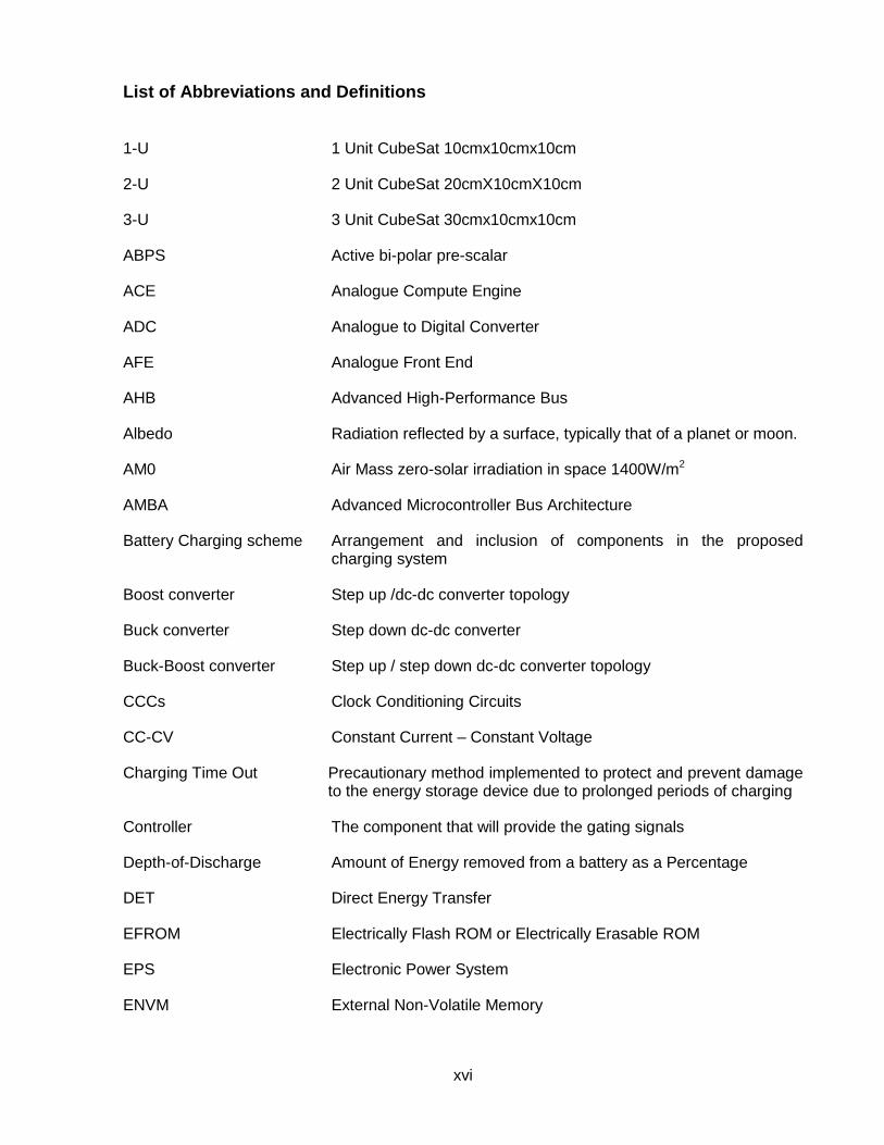
List of Abbreviations and Definitions
1-U 1 Unit CubeSat 10cmx10cmx10cm
2-U 2 Unit CubeSat 20cmX10cmX10cm
3-U 3 Unit CubeSat 30cmx10cmx10cm
ABPS Active bi-polar pre-scalar
ACE Analogue Compute Engine
ADC Analogue to Digital Converter
AFE Analogue Front End
AHB Advanced High-Performance Bus
Albedo Radiation reflected by a surface, typically that of a planet or moon.
AM0 Air Mass zero-solar irradiation in space 1400W/m2
AMBA Advanced Microcontroller Bus Architecture
Battery Charging scheme Arrangement and inclusion of components in the proposed charging system
Boost converter Step up /dc-dc converter topology
Buck converter Step down dc-dc converter
Buck-Boost converter Step up / step down dc-dc converter topology
CCCs Clock Conditioning Circuits
CC-CV Constant Current – Constant Voltage
Charging Time Out Precautionary method implemented to protect and prevent damage to the energy storage device due to prolonged periods of charging
Controller The component that will provide the gating signals
Depth-of-Discharge Amount of Energy removed from a battery as a Percentage
DET Direct Energy Transfer
EFROM Electrically Flash ROM or Electrically Erasable ROM
EPS Electronic Power System
ENVM External Non-Volatile Memory

xvii
FPGA Field-Programmable-Gate-Array
Geostationary Earth Orbit 35786 km above the earth’s surface
GPIO’s General Purpose User Inputs and Outputs
Ground-Station Designated area used to monitor and acquire data from a satellite
High Charging Temperature Precautionary method implemented to protect and prevent damage to the energy storage device due to elevated temperatures during charging
I2C Inter Integrated Circuit
Krad Absorbed radiation dose in silicone (1 rad = 100 Grey)
Lithium-ion battery Energy storage device considered in this battery charging scheme
Low Earth Orbit 200 km to 2000 km above the earth’s surface
Medium Earth Orbit 2000 km to 20 000 km above the earth’s surface
MPU Micro Processor Unit
MPPT Maximum Power Point Tracking
Nano-satellite Artificial Satellite with a mass between 1 to 10 kg
On-orbit Operational area of a satellite
Over charging protection Precautionary method implemented to protect and prevent damage to the energy storage device due to over-charging conditions
PDMA Peripheral Direct Memory Access
PPE Post Processing Engine
P-POD Poly-PicoSatellite Orbital Deployer
SAR Successive approximation register
Solar Array A collection of solar cells (also known as solar panel)
Space Heritage Component proven to operate efficiently in space
SPI Serial Peripheral Interface
SSE Sample Sequencing Engine
VHDL VHSIC Hardware Description Language
VHSIC Very High Speed Integrated Circuit

xviii
Nomenclature
A Area of cells in cm2
a arbitrary constant
C capacity in amp-hours
E Energy stored in Watt-Hours
Ipv output current
Iph photo current
Isat diode reverse saturation current
Is_3.3 current during sun exposure on the 3.3V bus
Is_5 current during sun exposure on the 5V bus
Ie_3.3 current required during eclipse on the 3.3V
Ie_5 current during eclipse on the 5V bus
Is diode 1 saturation current Is2 diode 2 saturation current Icharge charge current
Jmpp current per cm2 at peak power
K Boltzmann’s constant
N1 diode 1 emission coefficient
N2 diode 2 emission coefficient
N solar cell ideality factor
ns number of solar cells in series
np number of solar cells in parallel
n(side) number of solar cells on the side panels
n(top) number of solar cell on the top panel
Pd power dissipated
Pout(side) output power of the side panels
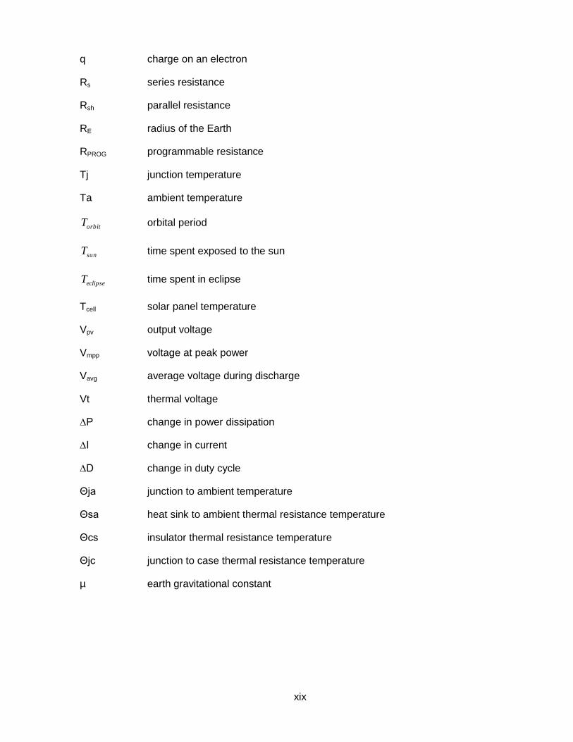
xix
q charge on an electron
Rs series resistance
Rsh parallel resistance
RE radius of the Earth
RPROG programmable resistance
Tj junction temperature
Ta ambient temperature
orbitT orbital period
sunT time spent exposed to the sun
eclipseT time spent in eclipse
Tcell solar panel temperature
Vpv output voltage
Vmpp voltage at peak power
Vavg average voltage during discharge
Vt thermal voltage
∆P change in power dissipation
∆I change in current
∆D change in duty cycle
Θja junction to ambient temperature
Θsa heat sink to ambient thermal resistance temperature
Θcs insulator thermal resistance temperature
Θjc junction to case thermal resistance temperature
µ earth gravitational constant

1
Chapter 1
Introduction
1.1 Background
Aspiring satellite engineers in South Africa have the opportunity to enrol at the Cape Peninsula
University of Technology (CPUT) in partnership with the French South African Institute of
Technology (F’SATI) to complete a two year dual Master’s Degree in Satellite Engineering (IAC,
2011). F’SATI was established in 1996 through collaboration between the French and South
African Governments in an effort to increase human capacity in this developing field in South
Africa. With the passing of the South African National Space Agency Act, a number of key role
players such as the National Research Foundation (NRF), Paris Chamber of Commerce, CPUT
and other well-established organisations have shown an increasing interest in the future of the
South African Space Industry.
The satellites being developed are CubeSats with dimensions of 10cm-by-10cm-by-10cm typical
of a 1-U. A complete 1-U CubeSat called ZACUBE-01 has already been developed and is
awaiting a launch date. The 1-U mission was designed, together with the South African National
Space Agency (SANSA) SPACE SCIENCE division, in order to use this particular CubeSat to
calibrate an array of transmitters in Antarctica, known as SuperDarn (Super Dual Auroral Radar
Network) (Greenwald, 1999). Funding has been secured for the further development of a 3-U
CubeSat with anticipated completion in 2015.
The CubeSat standard started as an effort between Prof. Jordi Puig-Suari at California
Polytechnic State University, San Luis Obispo, and Prof. Bob Twiggs at Stanford University’s
Space System Development Laboratory (SSDL) with the intention of creating a standard for
nano-satellites which will decrease the development cost, decrease the development time and
increase the accessibility to space through the implementation of the Poly-PicoSatellite Orbital
Deployer(P-POD) (Nason, Creedon, & Johansen, 2002).

2
1.2 Problem Statement
FPGAs have not yet been implemented on CubeSat electronic power supply sub-systems as it is
perceived that these devices consume relatively large amounts of power. This research
investigates whether the implementation of an FPGA-based electronic power supply sub-system
will optimise functionality by addressing the size, weight and power challenges (otherwise known
as SWAP challenges) presented by the CubeSat standard.
1.3 Objectives of the Research
Augmentation of the Electronic Power System (EPS) using an FPGA as the main controller will
address the SWAP constraints of the CubeSat standard. The specific objectives are listed as
follows:
Design a high-level CubeSat power budget according to specified requirements
considering the environment in space, orbital parameters, critical sub-systems, payloads
and duty cycle of operation of these sub-systems.
Investigate the solar cell and battery technologies and determine the solar array (SA)
size and the capacity of the secondary source of power (batteries).
Investigate various maximum power point tracking methods and determine which method
is best suited for the design and implementation in the field-programmable-gate-array.
Develop a flow chart of the algorithm chosen and write a suitable application code to be
implemented using the field-programmable-gate-array.
Utilise an FPGA as the main controller of the EPS sub-system:
o The FPGA should be chosen through comparative studies while considering the
application as well as the SWAP constraints.
o The FPGA should implement the necessary logic and algorithms while
considering the SWAP constraints.
o The FPGA feasibility in a nano-satellite EPS sub-system must be determined.
Choose an appropriate architecture while considering the SWAP constraints.
Illustrate the various design steps followed in order to implement the design.
Design and develop an EPS prototype to be used as proof of concept of operation.
Conduct stand-alone tests to verify the correct operation of the prototype and proof of
concept.
3
1.4 Research Methodology
First a literature review was done to establish the effects of the environment in space on the
electronics found within an Electrical Power Sub-System (EPS), also taking into consideration
that the orbit greatly affects which space environmental factors to consider. Research was then
directed into solar cell and battery technologies in order to establish which technologies best suit
the design requirements, followed by an extensive investigation into FPGA technology and the
VHDL programming language.
Different charging topologies were investigated, taking into account the different battery
chemistries and the implementation of maximum power point tracking algorithms. Subsequently,
power conditioning topologies were investigated and compared in order to meet the power
budget requirements.
This was followed by the designing of each sub-circuit of the sub-system, simulating the different
sub-circuits, procurement of components, construction and testing of individual sub-circuits and
a final orbital simulation test of the integrated prototype.
1.5 Delineation of the Research
A mock mission needs to be created to establish the necessary sub-system requirements in
order to fully delineate the research. These sub-system requirements, based on previous
CubeSat missions, will allow for accurate power consumption estimations. The design of an EPS
system usually starts with a power budget, a tool used by engineers to estimate the amount of
power that will be required to drive all the subsequent sub-systems; however, in a real world
situation, the power budget is subject to change.
At this stage, the power budget is an estimation of the incoming power, outgoing power, and
stored power as well as the expected maximum power. The incoming power is the power that is
converted from solar irradiance while the outgoing power is the power that is utilised by the sub-
systems. Maximum power should be able to allow the operation of all sub-systems for a certain
period of time.
The sub-systems that will be considered are the EPS, On-Board-Computer(OBC),
communication system and a camera as a payload. These sub-systems’ (e.g. communication,
payload, OBC) power consumptions are to be simulated during testing using an active load. The

4
on-time of these sub-systems are directly related to the orbit of the satellite; for instance, the
communication system transmits (Tx) only during the period when the satellite has a direct line
of sight with respect to the ground-station, while the receiving (Rx) of instruction should always
be enabled so as not to lose contact/control of the CubeSat. The payloads are only active over
areas of interest while the OBC and the EPS are the only sub-systems that should remain active
throughout the entirety of the mission as they are responsible for the majority of the critical
functions.
1.6 Significance of the Research
The size, weight and power constraints of CubeSats are the limiting factors in the engineering
design process of these satellites. So if engineers are able to overcome these constraints, larger
more expensive satellites may not be necessary. By optimising this particular sub-system, the
entire satellite will be allowed to operate more efficiently which in turn will allow CubeSats to
increase their overall efficiencies. The engineers at ClydeSpace have shown that there is a
market for small satellites in the world as their popularity is ever-increasing. Engineers have
shown that the true potential of CubeSats lies within the large number of CubeSats that can be
produced and used within a swarm of satellites to have multiple overpasses over a particular
area, known as a high temporal resolution. With the completion of this project, the working
prototype may be further developed into a flight ready model sub-system which will be an
intellectual property of CPUT. CPUT will have the opportunity to exploit the growing market of
CubeSats.
1.7 Structure of the Dissertation
Following this introductory chapter, Chapter 2 provides a literature overview of the nano-satellite
power system including space environment, battery technologies, field-programmable-gate-
arrays and various Maximum Power Point Tracking (MPPT) algorithms. Chapter 3 includes the
design solution of the nano-satellite power system including development of the power budget,
battery sizing, FPGA functionality, MPPT algorithm employed, development of the distribution
system and design of an active load. Chapter 4 deals with the practical construction of the
various sub-circuits of the EPS sub-system and FPGA implementation of the design. Chapter 5
covers the results of the nano-satellite power system, while Chapter 6 concludes the findings
and provides recommendations for further research.

5
Chapter 2
Nano-Satellite Power Systems and the Environment in Space
2.1 Nano-Satellite Power System Overview
The 10x10x10cm3 dimensions of the CubeSat 1-U standard place a large number of constraints
on the design of such a nano-satellite. These constraints are known as the size, weight and
power (SWAP) constraints. Engineers aim to place as much technology as possible in a 1-U
CubeSat in order to increase its functionality. However, a key area to be addressed is the
availability of power. Due to the environment in space, solar energy is the most preferred source
of power available to satellites in general; thus, the efficiency of a satellite depends on how well
each sub-system utilises the energy made available by the solar cells and the efficiency of the
solar cell itself.
Figure 2.1: Overview of a nano-satellite Electronic Power System (EPS) (Akagi, J. n.d)
Figure 2.1 shows the main components of an EPS found within nano-satellites, as well as EPS
sub-systems designed by ClydeSpace and GomSpace (GomSpace, 2012; Clyde Space, 2010).
These include solar cells, a step-up converter (MPPT circuit), a battery charger, a secondary

6
source of power (battery), command and data handling units, and dc-dc converters (distribution
system).
The design of the EPS starts with the mission requirements, taking into account the space
environment, power requirements of the payload and other critical sub-systems as well as
mission lifetime. From these requirements, the solar cell technology, battery technology and
distribution architecture may be chosen according to beginning-of-life (BOL) and end-of-life
(EOL) requirements.
2.2 Space Environment
2.2.1 Orbital Parameters
The orbital parameters are fixed values with small amounts of variance caused by orbit
degradation. Orbital parameters are chosen to suite a particular mission. Hence the design
process of any satellite sub-system strongly depends on these parameters. These orbital
parameters have a direct implication on the satellite’s operation. Factors such as the time spent
in the sun and time spent in eclipse are governed by these parameters. The parameters to be
dealt with include the following: the type of orbit, orbital height, inclination, time spent in the sun,
time spent in eclipse, average orbits per day, and average orbits for the extent of the mission.
Satellites that are in orbit are classified according to their height above the earth. These heights
are typically in one of these classifications: Geostationary Earth Orbit (GEO), Medium Earth
Orbits (MEO), or Low Earth Orbit (LEO). The differences in orbital heights are tabulated in Table
2.1.
Orbital height, together with the inclination of the orbit, affect the period of the satellite’s orbit as
well as the time spent in the sun and eclipse. The following formula (Equation 2.1) was used to
calculate the orbital period:
3
2a
Torbit
(2.1)
where a is RE(km) + orbit altitude(km), RE is the radius of the earth (6378 km) and µ is the
Earth’s gravitational constant (3.986005.104m3/s2)

7
Table 2.1: Space environment classification
Orbit Height
GEO 35786 km
MEO 2000 km to 20 000 km
LEO 200 km to 2000 km
By calculating the orbital period, the time spent in the sun and eclipse may be calculated with
Equations 2.2, 2.3 and 2.4 below:
orbitsun TT
0
0
360
2180
(2.2)
Where Tsun is the time spent in the sun in minutes
orbiteclipse TT
0
0
360
2180
(2.3)
Where Teclipse is the time spent in eclipse in minutes
α is calculated from
HR
R
E
E1cos
(2.4)
Where H is the altitude of the satellite above the earth’s surface.
From these calculations, the total number of charge/discharge cycles required by the battery
and the average depth of discharge (DoD) are both determined. These are critical factors as
they influence battery sizing.
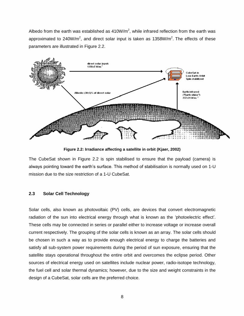
8
Albedo from the earth was established as 410W/m2, while infrared reflection from the earth was
approximated to 240W/m2, and direct solar input is taken as 1358W/m2. The effects of these
parameters are illustrated in Figure 2.2.
Figure 2.2: Irradiance affecting a satellite in orbit (Kjaer, 2002)
The CubeSat shown in Figure 2.2 is spin stabilised to ensure that the payload (camera) is
always pointing toward the earth’s surface. This method of stabilisation is normally used on 1-U
mission due to the size restriction of a 1-U CubeSat.
2.3 Solar Cell Technology
Solar cells, also known as photovoltaic (PV) cells, are devices that convert electromagnetic
radiation of the sun into electrical energy through what is known as the ‘photoelectric effect’.
These cells may be connected in series or parallel either to increase voltage or increase overall
current respectively. The grouping of the solar cells is known as an array. The solar cells should
be chosen in such a way as to provide enough electrical energy to charge the batteries and
satisfy all sub-system power requirements during the period of sun exposure, ensuring that the
satellite stays operational throughout the entire orbit and overcomes the eclipse period. Other
sources of electrical energy used on satellites include nuclear power, radio-isotope technology,
the fuel cell and solar thermal dynamics; however, due to the size and weight constraints in the
design of a CubeSat, solar cells are the preferred choice.

9
2.3.1 Solar Cell Theory
Solar cells operate on the basis of the photoelectric effect (Figure 2.3), an effect which occurs
when photons of the electromagnetic radiation produced by the sun strike a semiconductor
material. Maini and Agrawal (2007) explain that these photons can reflect off the surface of the
semiconductor material, pass through the semiconductor material without striking anything, or
be absorbed by electrons in the semiconductor material’s crystal lattice. Once these photons
are absorbed and excite the electrons in the material’s crystal lattice, the electrons which are
tightly bound in covalent bonds between atoms are able to move freely throughout the material.
The electrons leave behind an electron ‘hole’ which can then be filled by another electron of a
nearby atom creating another electron ‘hole’. These electron-hole pairs then move throughout
the semiconductor material driven by either an electrostatic field established across the material
or by gradient in the electrochemical composition. The movement of these electrons throughout
the material creates current and can be used to drive external loads.
Figure 2.3: Photoelectric effect (Horner, 2011)
The movement of the photons straight through the crystal lattice and the reflection thereof
decrease the efficiency of the solar cell. Table 2.2 compares various solar cell technologies
considered for this design.

10
Table 2.2: Solar cell technology comparison
Company Solar cell
Description
Mass Type Min
Efficiency
Dimensions
EMCORE Triple-Junction
Satellite Solar
Cell
84 mg/cm2 Germanium
Triple
Junction
28.5% 26.6 cm2 x 140 μm
(also custom
available)
EMCORE Triple-Junction
w/ Monolithic
Diode
84 mg/cm2 Germanium
Triple
Junction
28.0% 26.6 cm2 x
140 μm
(also custom
available)
EMCORE Adv. Triple
Junction (ATJ)
84 mg/cm2 Germanium
Triple
Junction
27.5% 26.6 cm2 x
140 μm
(also custom
available)
EMCORE Adv. Triple-
Junction w/
Monolithic
diode
84 mg/cm2 Germanium
Triple
Junction
27.0% 27.5cm2 x
140 μm
(also custom
available)
Spectrolab Next Triple
Junction (XTJ)
Solar Cells
84 mg/cm2 Germanium
Triple
Junction
29.9% Up To
60 cm2 x
140 μm
Spectrolab Ultra Triple
Junction (UTJ)
Solar Cells
84 mg/cm2 Germanium
Triple
Junction
28.3% Up to
32 cm2 x
140 μm
Spectrolab Improved
Triple
Junction (ITJ)
Solar Cells
84 mg/cm2 Germanium
Triple
Junction
26.8% Up to
31 cm2 x
175 μm
Sources: 1) Emcore. (2006). 2) Spectrolab.(2010)
Manufacturers such as Emcore and Spectrolab design solar cells such as the Advanced Triple
Junction (ATJ) and Next Generation Triple Junction (UTJ) depicted in Figure 2.4 which have
multiple layers of substrate - GaInP2, GaAs and Ge - with two junctions between the different
semiconductor materials.

11
Figure 2.4: UTJ solar cell structure (Spectrolab, 2010)
The various levels of substrate address the movement of photons straight through the solar cell
by increasing the total electron density of the solar cell, while anti-reflectives prevent the
reflection of solar irradiance. These solar cells can produce efficiencies of up to 29.3%
(Spectrolab, 2010).
These solar cells may be modelled using Kirchoff’s voltage and current laws, described further
in the following section.
2.3.2 Solar Cell Model
The aforementioned solar cells may be modelled using the circuit illustrated in Figure 2.5 from
Harjai et al. (2010). The circuit consists of a current source (Iph) used to represent the dislodging
of electrons within the crystal lattice, while Rse is the equivalent series resistance of the solar cell
and Rsh is the effective parallel resistance. The output of the current source is directly
proportional to the light falling on the cell.

12
Figure 2.5: Solar cell model (Harjai et al., 2010)
shDphpv IIII (2.5)
p
spho
cell
spho
satphpvR
RIV
NsnKT
RIVqIII 1exp
(2.6)
Using the information acquired from the solar cell data sheet, various solar cell characteristics
can be graphically illustrated using appropriate simulation packages. The output voltage and
current strongly depend on the illumination (Figure 2.6) and temperature characteristics of the
environment respectively. For this research, the 28.3% ultra-triple junction (UTJ) solar cells
were simulated to obtain results similar to that of Walker (2001).
Figure 2.6: I-V characteristics at various levels of irradiance

13
The model used to simulate the solar cell was based on published Matlab code by González-
Longatt (2005). The PSIMTM physical model was also used in conjunction with the Matlab code
to verify the results. The results obtained indicate that the current output of the solar cell is
highly dependent on the level of solar irradiance. It is seen that the maximum current occurs at
1400 W/m2 typically the level of irradiance that LEO satellites experience in the space
environment, as indicated in Figure 2.7. The current dramatically decreases as the level of solar
irradiance decreases; hence, it is expected that the power output of the solar cell follows a
similar trend (see Figure 2.7).
It is noted that the power increases with an increase in solar irradiance. The maximum power
voltage is found at 3.92V for all levels of irradiance, indicating that the solar cells can be
connected in parallel even if they are not experiencing the same level of solar irradiance. Figure
2.8 and Figure 2.9 indicate that the operating temperature of the solar cells affect the output
voltage and output power of the solar cell. The simulations indicate that as the temperature of
the solar cells increases, the output voltage and power decrease. This is an important factor to
note as the temperature of the CubeSat will be at a minimum as soon as it exits its eclipse
period and the output power will be at a maximum.
Figure 2.7: P-V characteristics at various levels of irradiance

14
Figure 2.8: I-V characteristic curve and different operating temperatures
Figure 2.9: P-V characteristic curves at different operating temperatures
2.3.3 Angle of Incidence
The angle of incidence (AOI) affects the output power of a solar cell due to the change of the
angle the sun makes with the solar cell while the satellite is in orbit (Bester, 2011). This change
is subject to the cosine rule where the angle changes through 00 to 900(Figure 2.10). Using
Equation 2.7, the output power can be calculated at any instance in the orbit by knowing the
angle between the incident light and the vector normal to the plane.

15
Figure 2.10: Angle of incidence
cosPP avgout , (2.7)
where Pout is the power at an incidence of 900 to the solar cell.
Maximum power can be generated from the solar array (SA) when three sides are exposed to
solar irradiance; however, the AOI varies throughout the entirety of the orbit. The formula
(Equation 2.8) describes the total power generated by three sides exposed to the sun with
varying AOI:
CosPSinSinPSinCosPP sidesidesidetotal 321 (2.8)
where Psidex is power generated by the side at normal incidence.
The output power of the solar array can be calculated using Equation 2.7.
mpppmppsout JAnVnP
(2.9)
top
side
)top(out)side(outn
nPP
(2.10)
Equations 2.9 and 2.10 can be used to calculate the solar panel average power using the
datasheet information of the electrical characteristics of the solar panel provided by the
manufacturer.

16
2.4 Secondary Power Source
Selecting the appropriate battery technology to be used in an electronic power system is a
critical step of the design process. The battery technology must be chosen so as to conform to
the size, weight and power limitations of the design. Due to the size and weight constraints of
the CubeSat standard, Li-polymer and Lithium-ion battery technologies were selected for use as
these batteries provide high volumetric energy densities as well as high gravimetric energy
densities in relatively small packages.
2.4.1 Different Battery Technologies
Table 2.3 provides a comparison between the different battery technologies used: Nickel-
Cadmium (NiCd), Nickel-Metal hydride (NiMH) and Lithium-Ion/Polymer Batteries.
Table 2.3: Battery technology comparison
Type NiCd NiMH Li- ion/ Po
Nominal voltage (V) 1.2V 1.2V 3.7V
Density of energy (W.h/l) 140 180 200
Density of energy (W.h/kg) 39 57 83
Maximum discharge current 20C 4C 2C
Charging time 15min 30min 60min
Thermal range for charging 0 to +50 0 to +45 0 to +60
Thermal range for discharge -20 to +50 -20 to +50 0 to +50
Resistance against overcharging low low middle
Cathode material NiOOH NiOOH LiPO
Anode material Cd Alloy C
Max. number of cycles 1000 500 400
Sources: 1) Sunica (n.d). Enertech International (2007); 2) Danionics (n.d.)

17
From Table 2.3 it can be seen that the volumetric and gravimetric energy densities are much
higher for Li-Po batteries. The maximum number of discharge cycles for the Li-Ion batteries are
400 cycles; however, this is only the case when the DoD of the batteries are 100% which will
not be allowed as this decreases a battery’s life cycle. DoD will be regulated to 20%. These
batteries have typical capacity ratings measured in mAh. A 1000mAh battery is able to supply
1000mA for an hour, or 100mA for 10 hours. In the design of the EPS sub-system, this capacity
rating must be carefully considered as it will determine the depth of discharge of the secondary
power source, the total number of cycles, and the charging current required to optimally charge
the battery. For example, to charge a 1000mAh battery, 1000mA is needed to charge the
battery in one hour if the battery is completely depleted. This is known as 1C or 100% of the
rated battery capacity.
In order to optimally charge the selected battery, a battery charger needs to be selected to
satisfy the charging conditions. This battery charger should take into consideration the battery
chemistry and be able to detect the state of charge (SOC) of the battery. Ni-Cd, Ni-MH and Li-
ion batteries are of different chemistries requiring their own unique charging methods and
needing to be fully discharged before starting the charging process in order to avoid a decrease
in capacity (a phenomenon known as the ‘memory effect’) while lithium-ion batteries require the
implementation of the constant-current constant-voltage charging method to reach their fully
charged state while having no danger of the memory effect (McLaren et. al, 2008; Davide, n.d.).
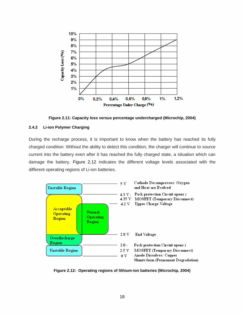
However, these batteries should not be undercharged as this could lead to a decrease in the
capacity of the lithium-ion battery. Figure 2.11 indicates the percentage loss against the
percentage under charge.
18
Figure 2.11: Capacity loss versus percentage undercharged (Microchip, 2004)
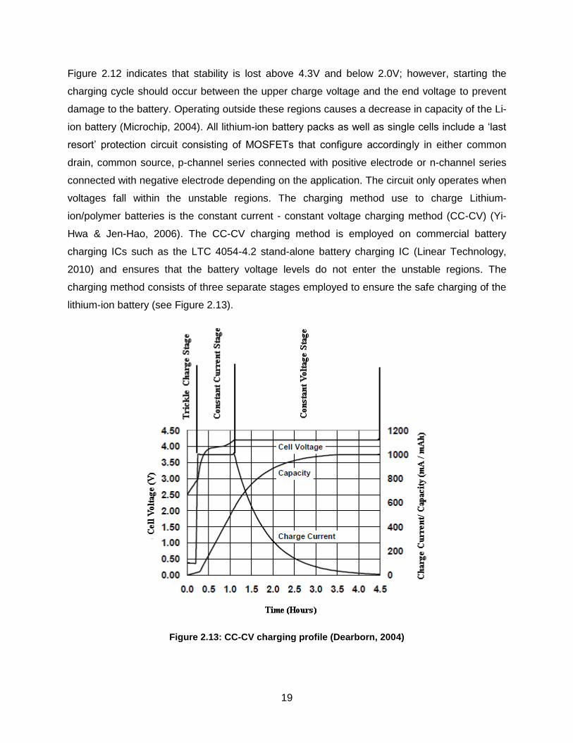
2.4.2 Li-ion Polymer Charging
During the recharge process, it is important to know when the battery has reached its fully
charged condition. Without the ability to detect this condition, the charger will continue to source
current into the battery even after it has reached the fully charged state, a situation which can
damage the battery. Figure 2.12 indicates the different voltage levels associated with the
different operating regions of Li-ion batteries.
Figure 2.12: Operating regions of lithium-ion batteries (Microchip, 2004)
19
Figure 2.12 indicates that stability is lost above 4.3V and below 2.0V; however, starting the
charging cycle should occur between the upper charge voltage and the end voltage to prevent
damage to the battery. Operating outside these regions causes a decrease in capacity of the Li-
ion battery (Microchip, 2004). All lithium-ion battery packs as well as single cells include a ‘last
resort’ protection circuit consisting of MOSFETs that configure accordingly in either common
drain, common source, p-channel series connected with positive electrode or n-channel series
connected with negative electrode depending on the application. The circuit only operates when
voltages fall within the unstable regions. The charging method use to charge Lithium-
ion/polymer batteries is the constant current - constant voltage charging method (CC-CV) (Yi-
Hwa & Jen-Hao, 2006). The CC-CV charging method is employed on commercial battery
charging ICs such as the LTC 4054-4.2 stand-alone battery charging IC (Linear Technology,
2010) and ensures that the battery voltage levels do not enter the unstable regions. The
charging method consists of three separate stages employed to ensure the safe charging of the
lithium-ion battery (see Figure 2.13).
Figure 2.13: CC-CV charging profile (Dearborn, 2004)

20
Trickle Charge Stage: Trickle charge is employed to restore charge to cells that have been
deeply depleted. Not utilising the trickle charge stage on deeply depleted cells damages the
lithium-ion battery and decreases the capacity. Trickle charge is employed when the battery cell
voltage falls within the ‘over discharge’ region. A constant current of 0.1C is used to charge the
cell until the cell voltage has reached 3.8V.
Fast Charge Stage: Once the cell voltage has risen above the trickle charge threshold of 3.8V,
the charge current is increased to less than 1.0C. Current is often ramped as the cell voltage
rises. This is done in order to minimise heat dissipation.
Constant Voltage Stage: This mode is entered once the cell voltage has reached 4.2V.
Charging at a voltage less than 4.2V may cause a decrease in battery capacity, as illustrated in
Figure 2.14. The voltage should be regulated within a tolerance of ±1% in order to ensure
maximum performance of the lithium-ion battery.
The charging process is terminated by sensing when the charge current drops below 7% of the
battery capacity, or 0.07C. Another termination criterion is the implementation of a timer that
times out the operation after a set amount of time, approximately two hours after the constant
voltage stage is initiated. Advanced chargers implement a combination of the two or may even
incorporate battery cell temperature, as this typically indicates when the battery has reached its
optimal capacity.
Figure 2.14: Loss in capacity at different charging voltages (Dearborn, 2004)

21
2.5 Field-Programmable-Gate-Arrays (FPGAs)
Digital Signal Processors (DSPs) and microcontrollers are most commonly used to implement
algorithms (Wu, 2003; Hohm & Ropp, 2000); however, due to the flexibility of Field-
Programmable-Gate-Arrays (FPGAs), FPGAs may offer equivalent or higher performance in
comparison to DSPs. Table 2.4 provides a comparison between different FPGAs from different
manufacturers. The features chosen for comparison are unique to the CubeSat design process
as it addresses the SWAP constraints. The design requires an integrated analogue interface, a
feature that allows the integration of multiple functions within the FPGA itself, while the FPGA
itself should not require much board space.
Table 2.4: FPGA technology comparison
Manufacturer Product Features
Actel SmartFusion Up to 500 000 system gates
Analogue Compute engine
8 direct analogue inputs
135 user I/0’s
IGLOO/e Up to 3 x 10 6 system gates
Flash*Freeze mode as low as 5 micro watt.
No direct analogue inputs
135 user I/0’s
ProASIC3 nano Up to 250 000 system gates
No direct analogue inputs
71 user I/O
Xilinx Spartan-6 Up to 150 000 Logic Cells
No analogue inputs available
576 user I/O

22
Virtex-6 Up to 760 000 Logic Cells
Analogue inputs available
576 user I/O
Virtex-7 Up to 2 x 10 6 Logic Cells
Analogue inputs available
1 200 user I/O
Altera
Cyclone Up to 20 060 Logic Elements
No analogue inputs available
301 user I/O
Cyclone II Up to 68 416 Logic Elements
Analogue inputs available
622 user I/O
Cyclone III Up to 119 088 Logic Elements
Analogue inputs available
622 user I/O
Sources: 1) Microsemi SoC (2011); 2) Xilinx (n.d.); and 3) Altera. (n.d.)
It can be seen that FPGAs are able to integrate a large number of technologies within a single
chip. Therefore, some functional blocks of the charging system may be implemented on an
FPGA chip in order to streamline the design and prototyping process. Yi-Hwa, Jen-Chung, and
Jen-Hao (2004) and Yi-Hwa and Jen-Hao (2006) proposed the design and implementation of a
fully digital lithium-ion battery charging system using an FPGA. These papers discuss the use of
an FPGA as the main controller, a multi-phase buck converter topology and a Graphical User
Interface (GUI) for monitoring the parameters of the charge/discharge cycles. They were able to
augment the charging of a lithium-ion battery to obtain an efficient charging cycle with charging
ripple current of less than 1%. Person (2004) implemented a maximum power point tracking
algorithm using an Altera FLEX 10K FPGA and produced an integrated MPPT system with ADC
interface, FIR filter, dither generator, and DAC interface within the same FPGA, thus
streamlining the prototyping process.

23
Table 2.5 provides FPGA technology and features from the Actel group. Products from Actel
were considered primarily due to the close relationship between CPUT and ASIC Design
Services, the sole vendor of Actel products in South Africa.
Table 2.5: Actel FPGA technologies (Microsemi SoC Product Group, 2011)
Products Features
SmartFusion Customisable System-on-Chip (cSoC)
Extended Temperature Fusion
Mixed signal integration down to -550C
Reprogrammable digital logic and configurable analogue
Embedded flash memory
IGLOO/e
Low power
Small package footprint
High logic density
IGLOO nano
Low power
Small package footprint
IGLOO plus
Low power
Small package footprint
High I/O-to-Logic ratio
ProASIC 3/E
High logic density
High performance
Low cost
Low power
ProASIC 3L
High logic density
High performance
Low cost
The IGLOO devices of Actel have a power consumption as low as 5µW implementing their flash
freeze mode with 30 000 available system gates and offering In-System Programming (ISP).
Xilinx offers top of the range FPGAs, with the Artix-7 having the lowest power consumption
mainly due to differences in available logic cells. The Artix-7 offers Agile Mixed Signal
(AMS)/XADC with 12-bit resolution, 600 I/O pins with 19Mb of blockRAM.

24
Considering these technologies, together with availability and cost, the SmartFusion FPGA was
selected as the main controller in this design.
The SmartFusion FPGA produced by Actel offers a customisable System-on-Chip (cSoC) that
integrates an ARM Cortex – M3 processor, programmable analogue together with the standard
FPGA fabric. The SmartFusion (cSoC) contains up to 500 000 system gates, a microcontroller
sub-system with I2C interface, and a 32KHz low power oscillator, 1 ADC (8-12 bit-SAR) and one
12-bit sigma-delta DAC. The structure and operation of this FPGA will be discussed in the
following section.
Figure 2.15: SmartFusion FPGA structure (Microsemi SoC Product Group, 2012)

25
2.5.1 Microcontroller Sub-System (MSS)
The MSS illustrated by the yellow section in Figure 2.15 possesses a 100 MHz Cortex-M3
processor capable of performing 125 million instructions per second (MIPS), and a multi-layer
AHB bus matrix (AHB) that connects various peripherals. The AHB bus matrix allows either the
Cortex-M3 processor, FPGA fabric master, Ethernet Message Authentication controller (MAC)
or peripheral DMA (PDMA) controller to act as masters to the integrated peripherals. These
integrated peripherals may include the FPGA fabric, embedded non-volatile memory (eNVM),
embedded synchronous RAM (eSRAM), external memory controller (EMC), and analogue
compute engine (ACE) blocks. This becomes an important factor as the MSS can handle
multiple operations required for the operation of the EPS sub-system (Actel Corporation, 2010).
2.5.2 Analogue Front-End (AFE)
The AFE consists of a successive approximation register of analogue-to-digital converters (SAR
ADC), first order sigma-delta digital-to-analogue converters (SDD DAC) and signal conditioning
blocks (SCBs). These SCBs are made of a combination of active bipolar prescalers (ABPS),
comparators to monitor fast signal thresholds without using the ADC, current monitors and
temperature monitors which allow the SmartFusion FPGA to handle multiple analogue signals
simultaneously, while the ABPS modules allow larger bipolar voltages to be fed to the ADC. An
external sense resistor is used to convert voltages into a suitable range for the ADC while the
temperature monitor is able to convert current internally by reading the current through an
external p-n junction.
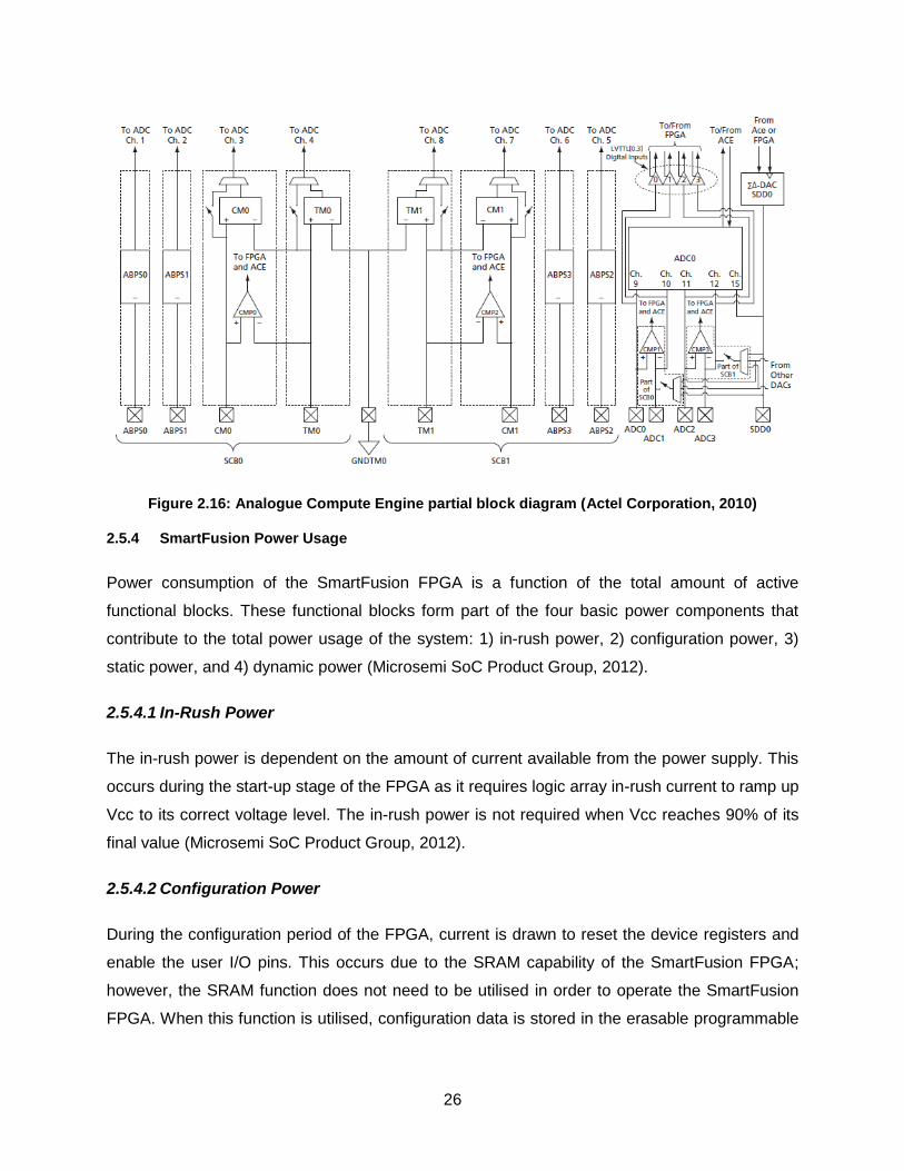
2.5.3 Analogue Compute Engine (ACE)
The various input signals are controlled and connected by the ACE. The ACE is a dedicated
processor designed to relieve the Cotex-M3 processor from handling the analogue blocks,
thereby allowing the Cortex-M3 processor to operate faster and with better overall power
consumption. The ACE is built to handle sampling, sequencing, and post-processing of the
ADCs, DACs, and SCBs. Figure 2.16 shows a block diagram of the ACE.
26
Figure 2.16: Analogue Compute Engine partial block diagram (Actel Corporation, 2010)
2.5.4 SmartFusion Power Usage
Power consumption of the SmartFusion FPGA is a function of the total amount of active
functional blocks. These functional blocks form part of the four basic power components that
contribute to the total power usage of the system: 1) in-rush power, 2) configuration power, 3)
static power, and 4) dynamic power (Microsemi SoC Product Group, 2012).
2.5.4.1 In-Rush Power
The in-rush power is dependent on the amount of current available from the power supply. This
occurs during the start-up stage of the FPGA as it requires logic array in-rush current to ramp up
Vcc to its correct voltage level. The in-rush power is not required when Vcc reaches 90% of its
final value (Microsemi SoC Product Group, 2012).
2.5.4.2 Configuration Power
During the configuration period of the FPGA, current is drawn to reset the device registers and
enable the user I/O pins. This occurs due to the SRAM capability of the SmartFusion FPGA;
however, the SRAM function does not need to be utilised in order to operate the SmartFusion
FPGA. When this function is utilised, configuration data is stored in the erasable programmable
27
read only memory (EPROM) which requires current to read from the look-up table (LUT). This
current is proportional to configuration power (Microsemi SoC Product Group, 2012).
2.5.4.3 Static Power
Static power refers to the idle condition of the FPGA; hence, no I/O activity and no clock inputs.
This occurs after the FPGA has been powered up and configured: static current flows
proportionally to the static power (Microsemi SoC Product Group, 2012).
2.5.4.4 Dynamic Power
The dynamic power of the SmartFusion FPGA is a function of all the operational activities of the
device. These activities include the operation of internal gates, registers in use, number of clock
lines, buffers, internal memory and any other switching of capacitive loads such as user I/O. It is
noticed that the dynamic power consumption is highly dependent on the switched capacitance,
routing capacitance and operating frequency (Microsemi SoC Product Group, 2012).
2.5.5 SmartFusion Power Calculation
The power consumption can be calculated using Equation 2.11 while including the number of
Phase Locked Loops (PLLs), clock conditioning circuits (CCCs), as well as the number and
frequency of each output clock, the internal clock frequencies and the number of I/O pins used
in the design, the analogue block used in the design, the temperature monitor, current monitor,
voltage monitor, ABPS, sigma-delta DAC, comparator, low power crystal oscillator, RC oscillator
and main crystal oscillator. Figure 2.17 provides the power supply configuration of the
SmartFusion FPGA.
DYNSTAT PPPTOTAL
(2.11)
where,
PSTAT is the total static power consumption and
PDYN is the total dynamic power consumption.
The total power consumption of the SmartFusion FPGA can be further reduced by allowing the
device to operate either in standby mode or time keeping mode. Microsemi has provided users
of the SmartFusion FPGA with an easy to use Power Calculator using a basic Microsoft Excel
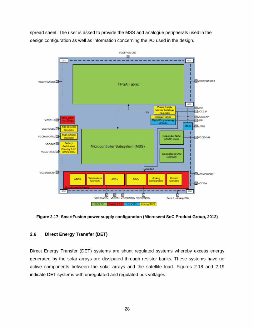
28
spread sheet. The user is asked to provide the MSS and analogue peripherals used in the
design configuration as well as information concerning the I/O used in the design.
Figure 2.17: SmartFusion power supply configuration (Microsemi SoC Product Group, 2012)
2.6 Direct Energy Transfer (DET)
Direct Energy Transfer (DET) systems are shunt regulated systems whereby excess energy
generated by the solar arrays are dissipated through resistor banks. These systems have no
active components between the solar arrays and the satellite load. Figures 2.18 and 2.19
indicate DET systems with unregulated and regulated bus voltages:
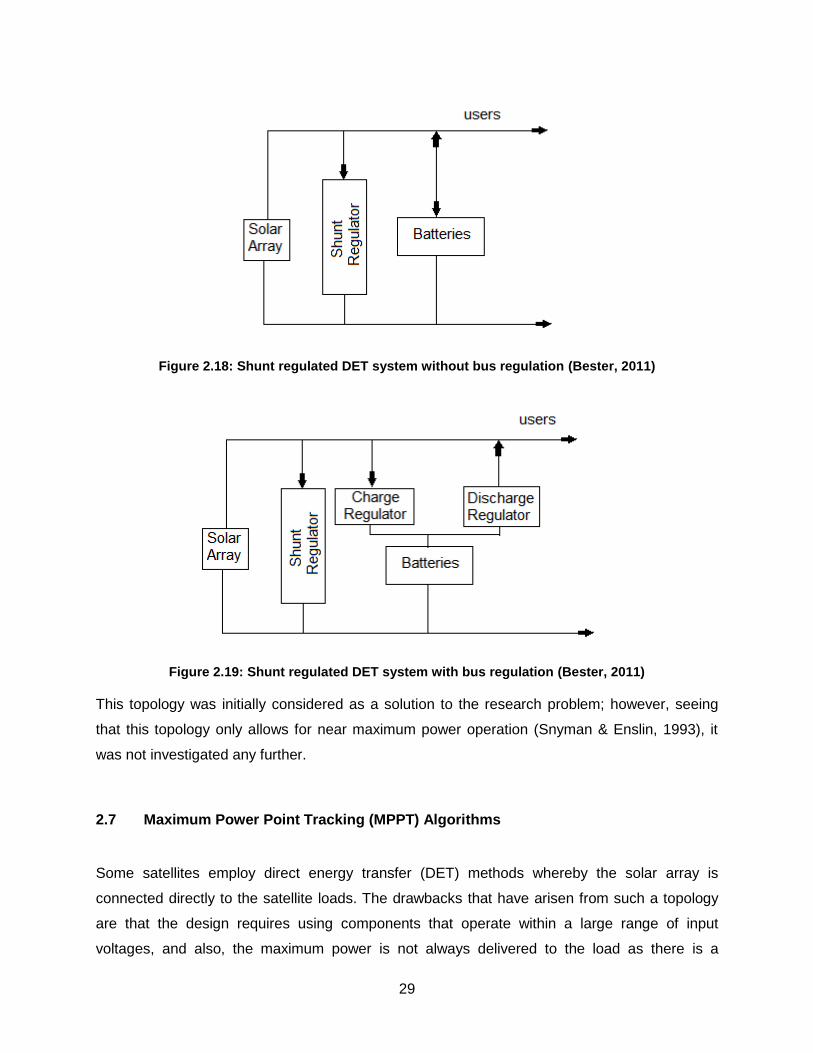
29
Figure 2.18: Shunt regulated DET system without bus regulation (Bester, 2011)
Figure 2.19: Shunt regulated DET system with bus regulation (Bester, 2011)
This topology was initially considered as a solution to the research problem; however, seeing
that this topology only allows for near maximum power operation (Snyman & Enslin, 1993), it
was not investigated any further.
2.7 Maximum Power Point Tracking (MPPT) Algorithms
Some satellites employ direct energy transfer (DET) methods whereby the solar array is
connected directly to the satellite loads. The drawbacks that have arisen from such a topology
are that the design requires using components that operate within a large range of input
voltages, and also, the maximum power is not always delivered to the load as there is a

30
mismatch between the source and load impedances. As illustrated in Figure 2.20, the maximum
power is a product of the solar cells characteristic open-circuit voltage and short-circuit current.
This point varies with increasing and decreasing levels of solar irradiance as well as changing
levels in operating temperatures, as discussed in Section 2.3.2. MPPT is achieved through the
implementation of algorithms to change the duty cycle of a dc-dc converter in order to match the
source and load impedances (Harjai et al., 2010). Some of these algorithms are discussed in
the next section.
Figure 2.20: Maximum power point (Clark & Simon, 2007)
2.7.1 Perturb-and-Observe
The implementation of this algorithm requires only one voltage sensor or an optional current
sensor in order to sense the voltage or current of the solar array. The perturb-and-observe
(P&O) algorithm is thus the most cost-effective and least complex method when compared to
other MPPT algorithms. The algorithm works by making small perturbations in the direction of
maximum power. However, this method does not consider rapid changes in the level of
irradiance which can lead to the calculation of the incorrect maximum power point.
2.7.2 Incremental Conductance
This method incorporates the use of two voltage and current sensors to sense output voltage
and current of the solar array. This algorithm (see Equation 2.12) calculates the slope of power

31
change to voltage of the solar array and suggests that at maximum power the slope of the solar
array is 0 watts.
dV/VIddV/dP MPP , (2.12)
MPPdV/VdII 0 ,
V/IdV/dI MPP .
By sensing both voltage and current, the rapid change in irradiance does not cause the
calculation of the wrong maximum power point, thus reducing the error due to rapid changes in
solar irradiance as opposed to the P&O method where this error is predominant (Ping et al.,
2011).
2.7.3 Fractional Open Circuit Voltage
A near linear relationship exists between the voltage at maximum power and the open circuit
voltage of the Solar Array. This relationship holds for variations in temperature levels and
irradiance. The implementation of this method works by creating a fractional open circuit in
order to measure the open circuit voltage and then compute the maximum power point voltage
using the linear relationship. This, however, causes a small interrupt in the power supply as the
converter is required to shut down momentarily.
2.7.4 Fractional Short Circuit Current
Similarly to the fractional open circuit voltage method, the fractional short circuit current method
relies on an approximated linear relationship between short circuit current and current at
maximum power under varying atmospheric conditions. The implementation of this method
requires an additional switch in order to periodically cause a short circuit across the Solar Array
in order to determine the value of the short circuit current and then determine the maximum
power point current using the linear relationship.
2.7.5 Neural Networks
Neural networks can consist of a large number of input parameters or nodes. These nodes are
embedded into the three layers of the neural network: 1) input layer, 2) hidden layer, and 3)
output layer. Neural networks are well-adapted for large microcontrollers as various input
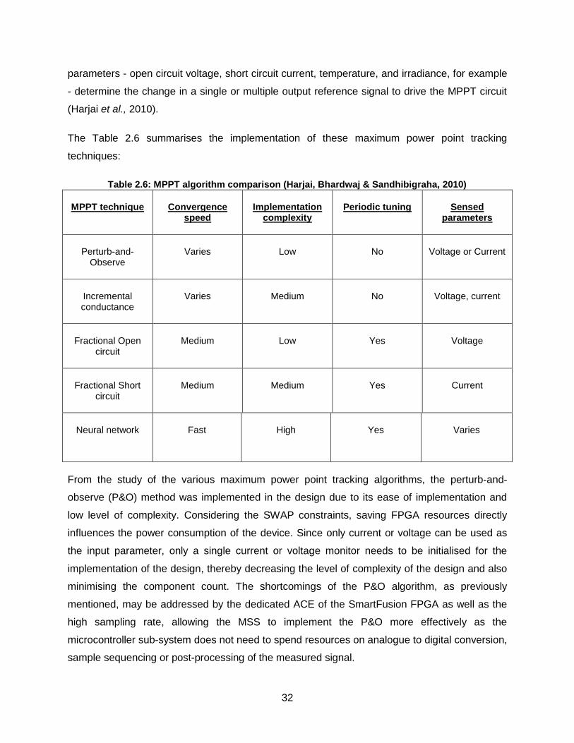
32
parameters - open circuit voltage, short circuit current, temperature, and irradiance, for example
- determine the change in a single or multiple output reference signal to drive the MPPT circuit
(Harjai et al., 2010).
The Table 2.6 summarises the implementation of these maximum power point tracking
techniques:
Table 2.6: MPPT algorithm comparison (Harjai, Bhardwaj & Sandhibigraha, 2010)
MPPT technique Convergence speed
Implementation complexity
Periodic tuning Sensed parameters
Perturb-and-Observe
Varies Low No Voltage or Current
Incremental conductance
Varies Medium No Voltage, current
Fractional Open circuit
Medium Low Yes Voltage
Fractional Short circuit
Medium Medium Yes Current
Neural network Fast High Yes Varies
From the study of the various maximum power point tracking algorithms, the perturb-and-
observe (P&O) method was implemented in the design due to its ease of implementation and
low level of complexity. Considering the SWAP constraints, saving FPGA resources directly
influences the power consumption of the device. Since only current or voltage can be used as
the input parameter, only a single current or voltage monitor needs to be initialised for the
implementation of the design, thereby decreasing the level of complexity of the design and also
minimising the component count. The shortcomings of the P&O algorithm, as previously
mentioned, may be addressed by the dedicated ACE of the SmartFusion FPGA as well as the
high sampling rate, allowing the MSS to implement the P&O more effectively as the
microcontroller sub-system does not need to spend resources on analogue to digital conversion,
sample sequencing or post-processing of the measured signal.

33
Chapter 3
Prototype Design and Simulation
3.1 Overview of Design Solution
This section gives a detailed description of the design process followed to obtain the objectives
of the EPS sub-system. A brief overview of the proposed solution is discussed, taking into
consideration the environment in space, average orbit power produced, sizing of the secondary
power source, maximum power point tracking and FPGA implementation. The section also
provides simulation results for the above mentioned factors as well as the distribution system
and active load design.
Figure 3.1: Proposed EPS design solution

34
Figure 3.1 provides a design overview of the proposed EPS sub-system. It consists of the
SmartFusion FPGA as the main controller implementing the MPPT algorithm on the solar cells.
The SmartFusion FPGA monitors various currents and voltages and provides the appropriate
control signal in order to maintain system stability. The solar cells produce an output voltage of
approximately 3.88V which is then boosted to 4.2V. This is done due to the normal operating
voltage of Li-ion batteries being 3.7V and charging occurring at 4.2V. The battery charger
receives an enable signal from the SmartFusion FPGA as soon as the battery voltage falls
below a pre-set value. The battery charger implements the CC-CV charging strategy, ensuring
that the optimal battery capacity is maintained. The distribution system consists of a boost
converter as well as a buck converter regulating the output voltages at 5V and 3.3V
respectively. The power delivery capability of each bus will be determined by completing a high
level power budget. The power budget will take into account various factors such as input
power, power losses, duration of sub-system activity and the power requirements for that
duration from which a secondary power source may be sized accordingly.
3.2 Orbital Parameters
Orbital parameters form part of the top-level mission specifications. Parameters such as orbital
height, inclination and orbital period play important roles in the mission as they will define the
type of payload that can be used. These parameters determine the amount of time spent in the
sun and thus the amount of time available for charging and the time spent in eclipse. The time
spent in eclipse is a critical window as it is vital that the CubeSat stay operational within this
window. The following equations are used to determine these critical parameters and are
summarised in Table 3.1.
3
2a
Torbit
(3.1)
From Equation 3.1:
14
3
109860053
80063782
.Torbit

35
23
141065851 a.Torbit
min.Torbit 86100
At an orbital height of 800km, an orbital period of approximately 100.86 minutes is expected.
Equations 3.2 and 3.3 provide an indication of the approximate time spent exposed to solar
irradiance and time spent in eclipse respectively:
orbitsun TT
0
0
360
2180
, (3.2)
orbiteclipse TT
0
0
360
2180
, (3.3)
Equation 3.4 is used to calculate the value of α:
8006378
63781cos ,
(3.4)
0308627. .
Using the value obtained from Equation 3.4, Equations 3.2 and 3.3 yield the following results:
min.
.Tsun 86100
360
30862721800
00
,
min.Tsun 731965 .
min86.100
360
3086.2721800
00
eclipseT ,
min.Teclipse 128135 .

36
Table 3.1: Orbital parameters
Orbital Parameter Specification
Orbit classification LEO
Orbital height 800 km
Inclination of orbit 3086.27 0
Period of orbit 101 min
Time spent in the sun 66 min
Time spent in eclipse 35 min
Orbits per day 14.26
Orbits during extent of mission life time 5204
The calculated parameters indicate that a total time of 66 minutes of the 101 minute orbit is
spent exposed to the sun. Sixty six minutes constitute 65.3% of the orbit allowed for battery
charging while providing the CubeSat with the necessary power for operation of payloads and
communication. Thirty five minutes is spent in eclipse, only allowing the operation of the critical
sub-systems to ensure that the CubeSat continues to receive commands (Rx) so as not to lose
contact/control of the CubeSat. The power budget will take these parameters into account and
is further developed later in this chapter.
3.3 Solar Cell Power Produced
The average orbit power is a function of the solar cell characteristics, total area of the solar cell,
and the angle of incidence as illustrated in Figure 3.2. Table 3.2 provides the electrical
characteristics of the UTJ solar cells from Spectrolab while Figure 3.2 provides the total area of
the aforementioned solar cells.

37
Figure 3.2: Solar cell area (Kjaer, 2002)
With the inspection of the solar cell layout (illustrated in Figure 3.3), it can be seen that each
side can only house two of these solar cells. Figure 3.4 shows a three dimensional rendition of
the solar cell layout. These solar cells are connected in parallel forming a one- series- two-
parallel (1s2p) configuration. The solar cells can be connected in a 2s1p configuration; however,
this would increase the total voltage of the system while the current produced remains that of
one cell. Connection in the 1s2p configuration allows for an increase in current output of the
solar cell while the voltage remains within the design limits. With the solar cell configuration
decided upon, area known and electrical characteristics identified, the average orbit power may
be calculated using the formula as indicated in Chapter 2. Equation 2.7 is used to calculate the
power at 90o angle of incidence; however, this is the maximum power that can be produced by
the solar cells, since the angle of incidence is always changing due to the CubeSat orbiting the
earth, as well as the fact that spin stabilisation is implemented in order to control the attitude of
the CubeSat. Equation 2.8 is used to calculate the power produced by the three sides as the
angle of incidence changes. Thus the maximum power per side can be calculated using
Equation 2.9, as this equation allows us to calculate the power produced according to the solar
cell (1s2p) configuration as discussed earlier. Equation 2.10 provides a relation between the
different sides. This formula becomes more effective when the solar cells are not of a
symmetrical configuration. A MATLAB® code (Appendix C) was implemented using Equation 2.8
in order to obtain the average orbit power produced by the solar cells.

38
b) Bottom solar cell configuration
Figure 3.4: 3-D rendition of proposed solar cell layout
a) Top and side solar cell configuration Figure 3.3: Solar cell layout

39
Table 3.2: UTJ electrical properties
Parameters < 32cm2
> 50cm2
Jsc 17.05mA/cm2 17.05mA/cm
2
Jmp 16.30mA/cm2 16.30mA/cm
2
Jload min avg 16.40mA/cm2
16.40mA/cm2
Voc 2.660V 2.660V
Vmp 2.350V 2.350V
Vload 2.310V 2.310V
Cff 0.85 0.85
Effload 28.0% 28.0%
Effmp 28.3% 28.3%
Table 3.3: Solar cell average power
Parameters Calculated values
Pmpp(top) 2.11W
Pmpp(side) 2.11W
Pmax(array) 2.9840W
Pavg(array) 2.1941W
The average power calculations were based on the MATLAB® script from Bester (2011). The
script file was modified and adjusted to meet the specifications of the solar cell layout as well as
the electrical characteristics of the UTJ 28.3% solar cell. The results are tabulated in Table 3.3.
Table 3.3 indicates that the expected average orbit power using the 1s2p solar cell configuration
yields an output of 2.19W while the maximum power is expected to be 2.9840W. The power
produced forms part of the CubeSat mission constraints as this factor would determine the
operating power available to the payloads and other critical sub-systems.

40
3.4 Power Budget and Secondary Power Source Sizing
Traditionally the power budget is the starting point of the satellite design process as this
contains information regarding the satellite payload and operational requirements of critical sub-
systems. The size of the satellite thus depends on the power required to be harnessed as the
primary source of power needs to be sized accordingly. However, the CubeSat design process
starts by calculating the amount of power available for the particular design, then determining
the power budget for the CubeSat and its payloads, and finally the prototype design.
As previously noted, simulations indicate that the average orbit power is expected to be 2.11W
and maximum power of 2.9840W. From this it can be determined whether or not the solar cells
are able to drive the necessary sub-systems as well as the size of the secondary power source
in order to overcome the eclipse period.
A high-level power budget was constructed using information from the existing ZA-CUBE 01
mission and CubeSat missions as specified in Appendix A. Appendix E shows the power budget
as constructed using Microsoft Excel. The power budget indicates the various sub-systems to
be included in the CubeSat, and the amount of power these sub-systems utilise during the
various periods of operation indicated in by the duty cycle column. The power budget is further
analysed and summarised in Table 3.4 while Table 3.5 and Table 3.6 indicate the active sub-
systems during the eclipse period and the period while exposed to the sun, respectively, also
indicating expected operating voltages and power.
From the power budget, which includes a design margin of 5% and a minimum expected system
efficiency of 76.5%, the power delivery capability of each distribution bus is determined. The 5V
distribution bus is expected to deliver a total amount of 1747.6mW, while the 3.3V distribution
bus is expected to be able to deliver a total amount of 1024.78mW. Calculations determine the
amount of current required by each distribution bus. Equation 3.5 is used to determine the
current of each of the two distribution busses.
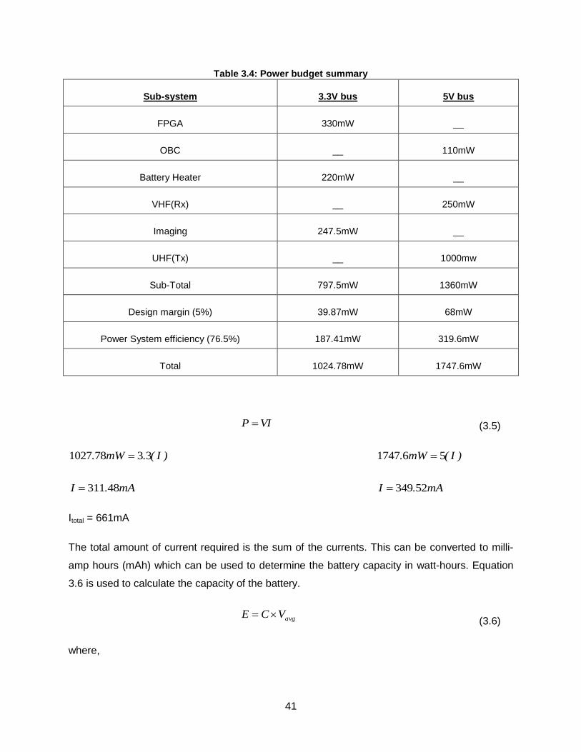
41
Table 3.4: Power budget summary
Sub-system 3.3V bus 5V bus
FPGA 330mW __
OBC __ 110mW
Battery Heater 220mW __
VHF(Rx) __ 250mW
Imaging 247.5mW __
UHF(Tx) __ 1000mw
Sub-Total 797.5mW 1360mW
Design margin (5%) 39.87mW 68mW
Power System efficiency (76.5%) 187.41mW 319.6mW
Total 1024.78mW 1747.6mW
VIP (3.5)
)I(.mW. 33781027 )I(mW. 561747
mA.I 48311 mA.I 52349
Itotal = 661mA
The total amount of current required is the sum of the currents. This can be converted to milli-
amp hours (mAh) which can be used to determine the battery capacity in watt-hours. Equation
3.6 is used to calculate the capacity of the battery.
avgVCE (3.6)
where,
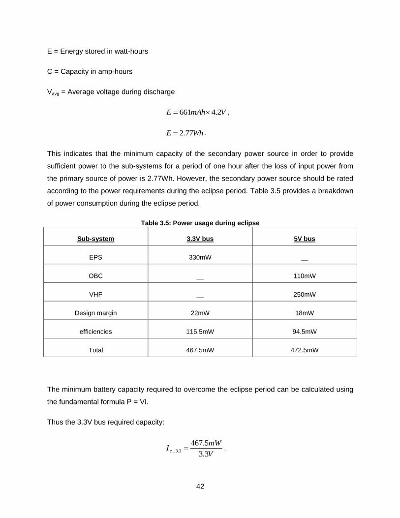
42
E = Energy stored in watt-hours
C = Capacity in amp-hours
Vavg = Average voltage during discharge
VmAhE 2.4661 ,
WhE 77.2 .
This indicates that the minimum capacity of the secondary power source in order to provide
sufficient power to the sub-systems for a period of one hour after the loss of input power from
the primary source of power is 2.77Wh. However, the secondary power source should be rated
according to the power requirements during the eclipse period. Table 3.5 provides a breakdown
of power consumption during the eclipse period.
Table 3.5: Power usage during eclipse
Sub-system 3.3V bus 5V bus
EPS 330mW __
OBC __ 110mW
VHF __ 250mW
Design margin 22mW 18mW
efficiencies 115.5mW 94.5mW
Total 467.5mW 472.5mW
The minimum battery capacity required to overcome the eclipse period can be calculated using
the fundamental formula P = VI.
Thus the 3.3V bus required capacity:
V
mWIe
3.3
5.4673.3_ ,

43
mAIe 7.1413.3_ .
5V bus required capacity:
V
mW.I _e
5
54725 ,
mA.I _e 5945 ,
Where Ie_3.3 is the current required during eclipse on the 3.3V bus and Ie_5 is the current during
eclipse on the 5V bus.
Thus, the total current can be calculated as follows:
5_3.3__ eetotale III , (3.7)
mAmAI totale 5.947.141_ ,
mAI totale 236_ .
The total eclipse period constitutes 34.82% of the total time spent in orbit amounting to 35.1281
minutes in eclipse. The secondary power source must be able to supply 236.2mA for 35.1281
minutes to overcome the eclipse period. The battery would therefore be operating at 236.2mAh
for a period of approximately 35.1281 minutes. The total amount of energy removed from the
battery during this period was found to be 580.808mWh.
Using Equation 3.6
avgVCE ,
VmA 2.42.236 ,
128.3560/04.992 mWh ,
mWh808.580 .
Calculating Depth-of-Discharge (DoD)
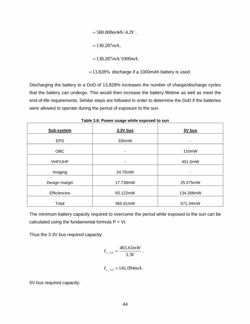
44
VmWh 2.4/808.580 ,
mA287.138 ,
mAmA 1000/287.138 .
%828.13 discharge if a 1000mAh battery is used.
Discharging the battery to a DoD of 13.828% increases the number of charge/discharge cycles
that the battery can undergo. This would then increase the battery lifetime as well as meet the
end-of-life requirements. Similar steps are followed in order to determine the DoD if the batteries
were allowed to operate during the period of exposure to the sun.
Table 3.6: Power usage while exposed to sun
Sub-system 3.3V bus 5V bus
EPS 330mW -
OBC - 110mW
VHF/UHF - 401.5mW
Imaging 24.75mW -
Design margin 17.738mW 25.575mW
Efficiencies 93.122mW 134.268mW
Total 465.61mW 671.34mW
The minimum battery capacity required to overcome the period while exposed to the sun can be
calculated using the fundamental formula P = VI.
Thus the 3.3V bus required capacity:
V.
mW.I ._s
33
6146533 ,
mA.I ._s 09414133 .
5V bus required capacity:
45
V
mW.I _s
5
346715 ,
mA.I _s 2681345 .
where Is_3.3 is the current during sun exposure on the 3.3V bus and Is_5 is the current during sun
exposure on the 5V bus.
Thus the total current can be calculated as follows:
5_3.3__ sstotals III ,
mAmAI totals 268.134094.141_ ,
mAI totals 362.275_ .
The total sun period constitutes 65.18% of the total time spent in orbit, amounting to 65.73217
minutes of sun exposure. The secondary power source must be able to supply 275.362mA for
65.73217 minutes to overcome the period of sun exposure if the solar cells were to fail. The
energy required was found to be 1267.009mWh and is calculated below:
Using Equation 3.6
avgVCE ,
VmA 2.4362.275 ,
73217.6560/520.1156 mWh ,
mWh009.1267 .
Calculating Depth-of-Discharge:
VmWh 2.4/009.1267 ,
mAh669.301 ,
mAhmAh 1000/669.301 ,

46
%167.30 discharge.
From the above calculations, Table 3.7 summarises the energy utilisation during the period of
eclipse, exposure to the sun, and total energy; however, in order to calculate the capacity of the
secondary source of power, only the parameters during eclipse are considered as a battery’s
main function is to provide enough energy to the CubeSat sub-systems in order to remain
functional throughout the eclipse period.
Table 3.7: Energy utilisation
Parameter Eclipse Sun exposure Total per orbit
Current 3.3V bus 141.7mA 141.094mA 282.794mA
5V bus 94.5mA 134.268mA 228.768mA
Energy 580.808mWh 1267.009mWh 1099.25mWh
DoD 13.828% 30.167% n/a
Table 3.8 indicates the battery characteristics in order to achieve the desired DoD and
overcome the eclipse period. These characteristics fall well into the SWAP constraints of the
CubeSat design as the battery technology chosen is of the Li-Ion/Polymer type and weighs
approximately 16g.
The average orbit power of 2.19W should be able to supply the payloads and sub-systems
during the period while exposed to the sun. This is calculated to determine whether or not the
batteries will be able to supply the loads if maximum power is drawn (i.e. all the loads are
operating at the same time) which is not advantageous as this would decrease the lifetime of
the batteries. Table 3.6 reveals that the total power on during the period while exposed to the
sun yields 1.137W, allowing for 1.053W to be utilised in order to charge the secondary source of
power.

47
Table 3.8: Battery characteristics required
Minimum Capacity 960mAh
Typical capacity 1000mAh
Nominal Voltage 3.7V
Charging method CC-CV
Charging Voltage 4.2V
Discharge voltage (cut-off) 2.75V
Charging current 500mA
Ambient temperature
Charge 0-400C
Discharge -20-600C
Storage -20-450C
Weight 16g±2g
Volumetric energy density 387Wh/l
Gravemetric energy density 200Wh/kg
Cycle life More than 500 cycles (to 80% initial capacity)
AC-impedance 60mΩ (at 1Khz frequency)
Nominal energy 3.7Wh (2W power load from 4.2V to 3.0V)
3.5 Perturb-and-Observe Maximum Power Point Tracking Algorithm
The Perturb-and-observe (P&O) maximum power point tracking algorithm is the most basic and
therefore the most commonly used MPPT algorithm. The algorithm was chosen due to the ease
of implementation and level of complexity, and because only a current or voltage input is
required to perform the algorithm. This becomes critically important as we are trying to save

48
FPGA resources utilised in this design as the amount of FPGA resources used directly affects
the power consumption of the FPGA device.
Measure V(i)
Measure I(i)
Start P& O MPPT
Algorithm
P(i)=V(i) x I(i)
∆P = P(i) - P(i-1)
∆I = I(i) – I(i-1)
∆P > o
∆I< 0∆I> 0
Increase Module
Current
Decrease
Module Current
Increase Module
Current
Decrease Module
Current
P(i) = P(i-1)
I(i) = I(i-1)
No Yes
No No YesYes
Figure 3.5: Perturb-and-observe MPPT algorithm
Figure 3.5 shows a flowchart of the P&O algorithm which starts by measuring the voltage V(i)
and current I(i) of the module. These values are used to calculate the power of the module.
These parameters are then stored and used to calculate the change in the total power
dissipation and voltage. When the difference between the last two power and current
measurements are positive or both are negative, an increase in module current is brought about
by increasing the duty cycle of the converter depicted in Figure 3.6 with a calculated value. This
value can be configured as the gradient of the power vs. voltage curve (Mellit et al., 2010)
ensuring that the perturbations of the duty cycle are well-matched with changes in
environmental conditions (i.e. changing level of solar irradiation). A decrease in the duty cycle of

49
the converter is brought about through a decrease in the difference between the power and an
increase in the difference of the current of the last two measurements. A decrease in duty cycle
can also be brought about by an increase in the difference between the power and a decrease
in the difference of the current between the last two measurements. This logic is summarised in
Table 3.9. Figure 3.6 shows the MPPT circuit diagram and indicates the closed loop control path
that is implemented in the dc-dc converter used in its implementation.
Table 3.9: P&O logic decisions
Power Current Duty cycle Decision
∆P > 0 ∆I > 0 +∆D Increase module current
∆P < 0 ∆I < 0 +∆D Increase module current
∆P > 0 ∆I < 0 -∆D Decrease module current
∆P < 0 ∆I > 0 -∆D Decrease module current
180uH
2SK2615 22uF
VoutVin
MPPT Signal from
SmartFusion FPGA
PV Array
To FPGA Current
Monitor
To FPGA Voltage
Sensor
50mΩ
Figure 3.6: MPPT implementation
The circuit diagram in Figure 3.6 shows the parameters to be measured by the SmartFusion
FPGA as well as the PWM control output signal required for maximum power point tracking
operation. The circuit design and design parameters are found in Appendix F.
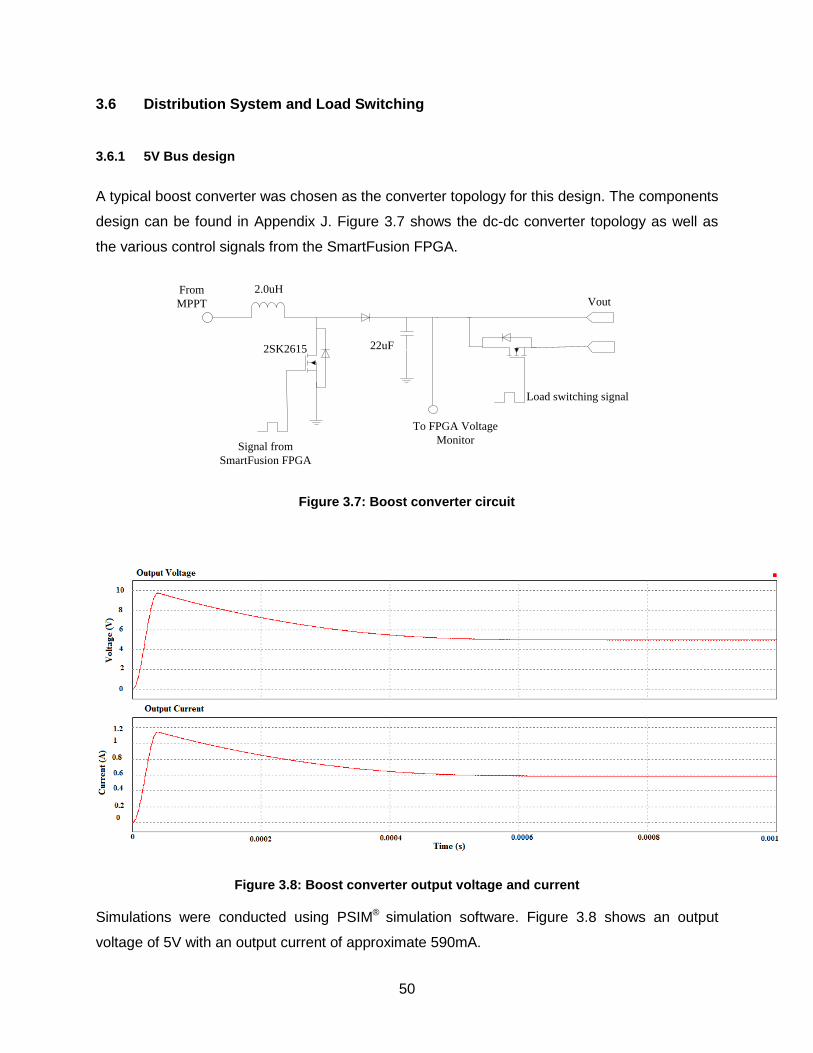
50
3.6 Distribution System and Load Switching
3.6.1 5V Bus design
A typical boost converter was chosen as the converter topology for this design. The components
design can be found in Appendix J. Figure 3.7 shows the dc-dc converter topology as well as
the various control signals from the SmartFusion FPGA.
2.0uH
2SK2615 22uF
VoutFrom
MPPT
Signal from
SmartFusion FPGA
To FPGA Voltage
Monitor
Load switching signal
Figure 3.7: Boost converter circuit
Figure 3.8: Boost converter output voltage and current
Simulations were conducted using PSIM® simulation software. Figure 3.8 shows an output
voltage of 5V with an output current of approximate 590mA.

51
3.6.2 3.3V Bus Design
The buck converter topology illustrated in Figure 3.9 was chosen to decrease the voltage from
4.2V to 3.3V. The components design can be found in Appendix J.
10uH
2SK2615 22uF
VoutFrom
MPPT
Signal from
SmartFusion FPGA
To FPGA Voltage
Monitor
Load switching signal
Figure 3.9: Buck converter circuit
Figure 3.10: Buck converter output voltage

52
Figure 3.11: Buck converter output current
Simulations were conducted using PSIM® simulation software. Figures 3.10 show an output
voltage of 3.3V with an output current of approximately 140mA indicated in Figure 3.11.
3.7 Active Load Design
The TIP 122 was used to produce an active load that can be used as a “dummy” load in order to
simulate the various payloads and sub-systems. The payloads and sub-systems to be simulated
by the active load are the following: battery heater, OBC, Imaging, and VHF and UHF antennas.
The active load was designed with a 10kΩ potentiometer in series with a 2kΩ resistor. A diode
D2, as illustrated in Figure 3.12 and Figure 3.14, was used to ensure current flowing through the
emitter to allow the correct operation of the TIP 122 power transistor. Circuits were designed to
be used on the 3.3V bus and 5V bus as illustrated by the aforementioned figures respectively.
The circuits were designed to handle a maximum of 5W on the 3.3V bus and 13W on the 5V
bus. This was done to simulate various load handling capabilities of the system. By varying the
potentiometer, the system response to changing load conditions can be examined.
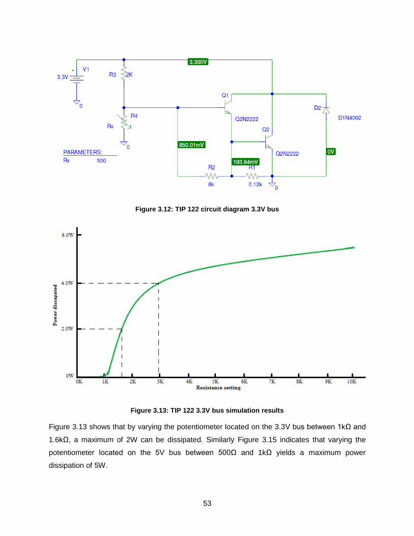
53
Figure 3.12: TIP 122 circuit diagram 3.3V bus
Figure 3.13: TIP 122 3.3V bus simulation results
Figure 3.13 shows that by varying the potentiometer located on the 3.3V bus between 1kΩ and
1.6kΩ, a maximum of 2W can be dissipated. Similarly Figure 3.15 indicates that varying the
potentiometer located on the 5V bus between 500Ω and 1kΩ yields a maximum power
dissipation of 5W.
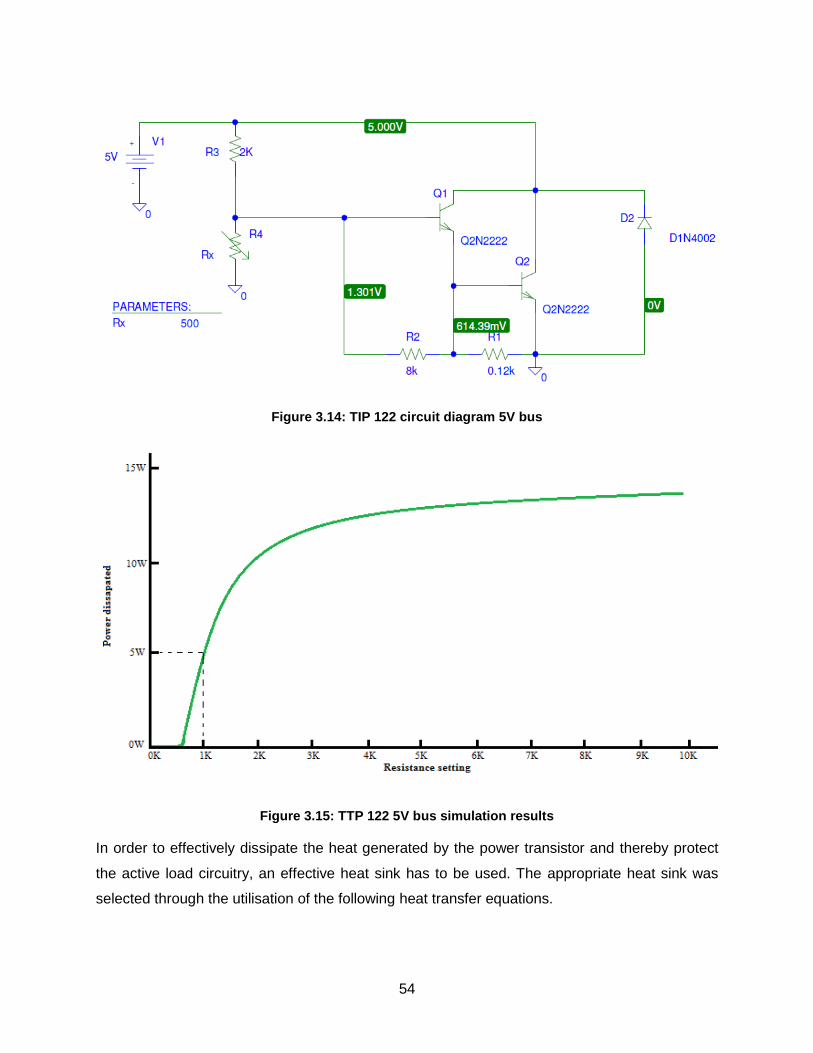
54
Figure 3.14: TIP 122 circuit diagram 5V bus
Figure 3.15: TTP 122 5V bus simulation results
In order to effectively dissipate the heat generated by the power transistor and thereby protect
the active load circuitry, an effective heat sink has to be used. The appropriate heat sink was
selected through the utilisation of the following heat transfer equations.

55
TasacsjcPdTj (3.8)
sacsjcja (3.9)
TajaPdTj (3.10)
Thus,
ja
TaTjP
(3.11)
562
30150
.P
W.P 921
1.92W is less than the required 10W.
Therefore,
P
TaTjja
(3.12)
10
30150 ja
W/Cja 012
To find the heat dissipating capability of the required heat sink, calculate Θsa:
csjcjasa (3.13)
52092112 ..sa
W/C.sa 0569
A heat sink with 9.56 oC/W was chosen to ensure the safe operation of the active load.

56
3.8 FPGA Functionality and Layout
The design uses analogue, software and hardware features of the SmartFusion FPGA. Table
3.10 provides a more detailed description of all the features to be utilised in the design of the
EPS sub-system.
Table 3.10: Utilisation of SmartFusion features
SmartFusion FPGA Features Utilised
Cortex-M3 Management of all components and functions
Processing and simple calculation
Software execution of less critical functions
UART,I2C Communication protocols with external
device/host/peer
Flash Code and parameter storage
SRAM Temporary code storage or boot
ADC and ACE Converts current into digital (used in Clark Transform)
Converts voltage into digital (used in Back-EMF)
Comparators used to catch faults
Analogue I/Os Analogue input of motor current and voltage
FPGA Hardware implementation of system critical tasks
Customised protocols and communication (CAN)
Customised algorithm (PID, SVPWM, etc.)
FPGA I/Os PWM outputs, encoder feedback, Hall sensor feedback
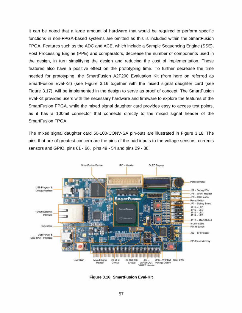
57
It can be noted that a large amount of hardware that would be required to perform specific
functions in non-FPGA-based systems are omitted as this is included within the SmartFusion
FPGA. Features such as the ADC and ACE, which include a Sample Sequencing Engine (SSE),
Post Processing Engine (PPE) and comparators, decrease the number of components used in
the design, in turn simplifying the design and reducing the cost of implementation. These
features also have a positive effect on the prototyping time. To further decrease the time
needed for prototyping, the SmartFusion A2F200 Evaluation Kit (from here on referred as
SmartFusion Eval-Kit) (see Figure 3.16 together with the mixed signal daughter card (see
Figure 3.17), will be implemented in the design to serve as proof of concept. The SmartFusion
Eval-Kit provides users with the necessary hardware and firmware to explore the features of the
SmartFusion FPGA, while the mixed signal daughter card provides easy to access test points,
as it has a 100mil connector that connects directly to the mixed signal header of the
SmartFusion FPGA.
The mixed signal daughter card 50-100-CONV-SA pin-outs are illustrated in Figure 3.18. The
pins that are of greatest concern are the pins of the pad inputs to the voltage sensors, currents
sensors and GPIO, pins 61 - 66, pins 49 - 54 and pins 29 - 38.
Figure 3.16: SmartFusion Eval-Kit
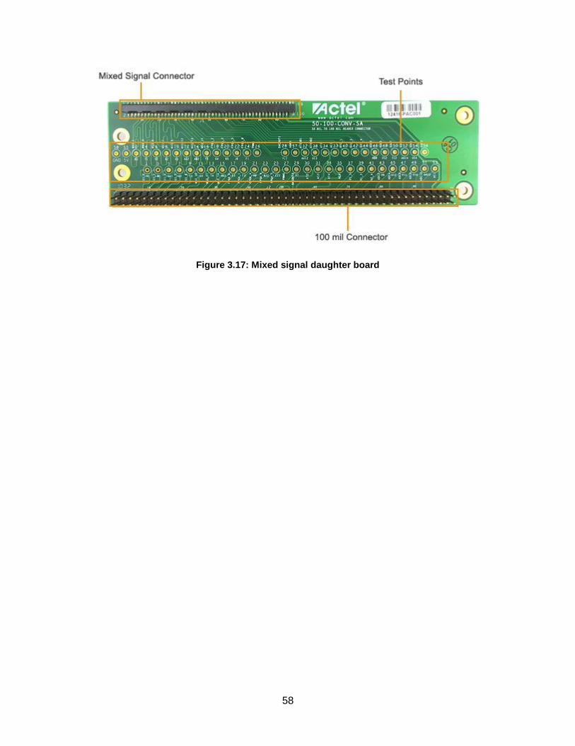
58
Figure 3.17: Mixed signal daughter board

59
Figure 3.18: Mixed signal connector

60
3.9 Matlab® Simulations
Figure 3.19: Matlab Simulation of MPPT implementation
The SimulinkTM model from Neeraj et al., illustrated in Figure 3.19, was modified with the solar
and MPPT characteristics used in this design. The model was modified to allow changes in the
solar irradiance that the CubeSat will experience in its operational environment. Figure 3.20
shows the series connection of six solar cells. The solar cell parameters are entered into the
block model, indicated in Figure 3.21. The block models the solar cell according to Equation
3.14, indicating the solar cell as a parallel combination of a current source, two exponential
diodes and a parallel resistor Rp, which is connected in series with Rs.
Rp
IRsV
VtN
IRsVqIs
VtNs
IRsVqIII oo
satphpv
1
*2
)(exp21
*exp
(3.14)

61
Figure 3.20: Solar cell model
Figure 3.21: Solar cell characteristics

62
The six solar cells indicated in Figure 3.20 are connected in parallel with three more of these
models, equalling a total of 24 solar cells. The solar cell connections used closely resemble the
characteristics of the solar cells to be used in the design. The solar cells used in prototyping are
further tested in Chapter 5. These solar cells have a typical open-circuit voltage of 0.538V,
short circuit current of 242mA and an assumed ideality factor (emission coefficient) of 1.2.
The P&O algorithm was implemented in the FPGA MPPT controller using a Matlab script file
attached in Appendix D. The output power, after the MPPT switch is enabled, was found to be
approximately 2.9W, illustrated in Figure 3.22. The maximum power point was found after
approximately 0.04 seconds, 0.02 seconds after MPPT activation (a detailed flowchart of the
algorithm implemented is presented in Section 4.6). By varying the irradiation level, the duty
cycle of the boost converter changes in order to keep the solar array operating at maximum
power.
Figure 3.22: MPPT output waveform

63
Chapter 4
Prototype Construction
4.1 Circuit Level Design Overview
DAC ADC0
GPIO
IN
Vdd OUT
Vcc
PROG
BAT GND
+ -
Li Ion
Battery
1000mAh
800k
3 2
2.2K
2K
5
4
EN
To Distribution SystemFrom Solar Cell Current Sense Resistor
180uH
2SK2615 10uF
MPPT
Battery Charger
FPGA
Figure 4.1: Basic circuit level design overview
The circuit shown in Figure 4.1 is a summarised version of the electronic power supply system.
A modular approach was taken in the circuit design to allow interconnection between various
circuit boards. This approach will allow the testing of different sub-circuits of the EPS individually
to determine each one’s functionality and operation, and then an orbital simulation test in which
the various systems are connected to each other will allow the testing of the full functionality of

64
the EPS prototype. The various sections of the design will be discussed in this chapter and
illustrate the prototypes constructed from the various designs.
4.2 Solar Cell
The solar cells (see Figure 4.2) obtained are from Futurlec.com. Ideally, solar cells from
Spectrolab (NeXt Triple Junction Solar Cells) can be used to increase the power produced;
however, due to both cost and availability, these solar cells were used in the test setup. Three of
these panels were obtained in order to provide the simulated environment to test to EPS sub-
system. The electrical properties are tabulated in Table 4.1.
Figure 4.2: Solar cell used in simulated environment
The 968mW solar cells have a high output current of approximately 242mA at maximum power
while producing a voltage of 3.88V. Various configurations were tested in order to provide the
power that closely resembles the conditions under which the EPS system is required to operate.

65
Table 4.1: Futurlec solar cell parameters
Parameter description Parameter value
Solar Cell Composition Polycrystalline
Peak Voltage (Vmp) 3.88V
Open-Circuit Voltage (Voc) 4.0V - 4.5V
Peak Current (Imp) 242mA
Short Circuit Current (Isc) 242mA – 261mA
Maximum Power (Pmax) 968mW
Dimensions (L x W x D) 120mm x 90mm x 2.8mm
4.3 Battery Charge/Discharge Circuit
The battery charge/discharge circuit forms a critical part of the EPS system. By using the
information from the power budget, a single lithium-ion battery was selected as the secondary
source of power of the nano-satellite. This is due to the sub-system requirements as stated in
Section 3.4. The battery characteristics state that a maximum charge current of 500mA is
required in order to charge the battery at C/2 while the solar cells are able to produce 726mA at
maximum power. The power budget indicates that a total of 275.362mA is required to power the
sub-system on both the 3.3V and 5V bus during period of sun exposure, leaving 450mA
available for charging.
There are a large range of commercially available lithium-ion battery charger integrated circuits.
The LTC4054 is a single cell lithium-ion battery charger using a constant-current/constant-
voltage algorithm, able to deliver up to 800mA of charge current. This charger would be ideal for
the system as it only requires 5V DC for operation, as indicated in Figure 4.3.

66
VCC
33uF
2.2K
2SK2615
Enable Signal
From FPGA
2
5
3
4
1
LTC4054-4.2
CHRG
VCC
GND
BAT
PROG
330Ω
Figure 4.3: LTC4054-4.2 Lithium-ion battery charger
The charge current is programmed using Equation 4.1, where RPROG is a single resistor from the
PROG pin to ground:
PROG
chrgR
VI
1000
(4.1)
Thus, in order to obtain a charge current of 450mA, a PROG resistor of 2.2kΩ is required.
However, in order to accommodate excess energy that may be generated during periods of low
power, a 1.2kΩ resistor may be utilised to dissipate excess energy and transfer this energy into
the secondary source of power. The battery charger will be used to maintain the charge of the
battery. This can be monitored using the FPGA by configuring the LTC4054-4.2 with two
different pull-up resistors, as indicated in Figure 4.4.
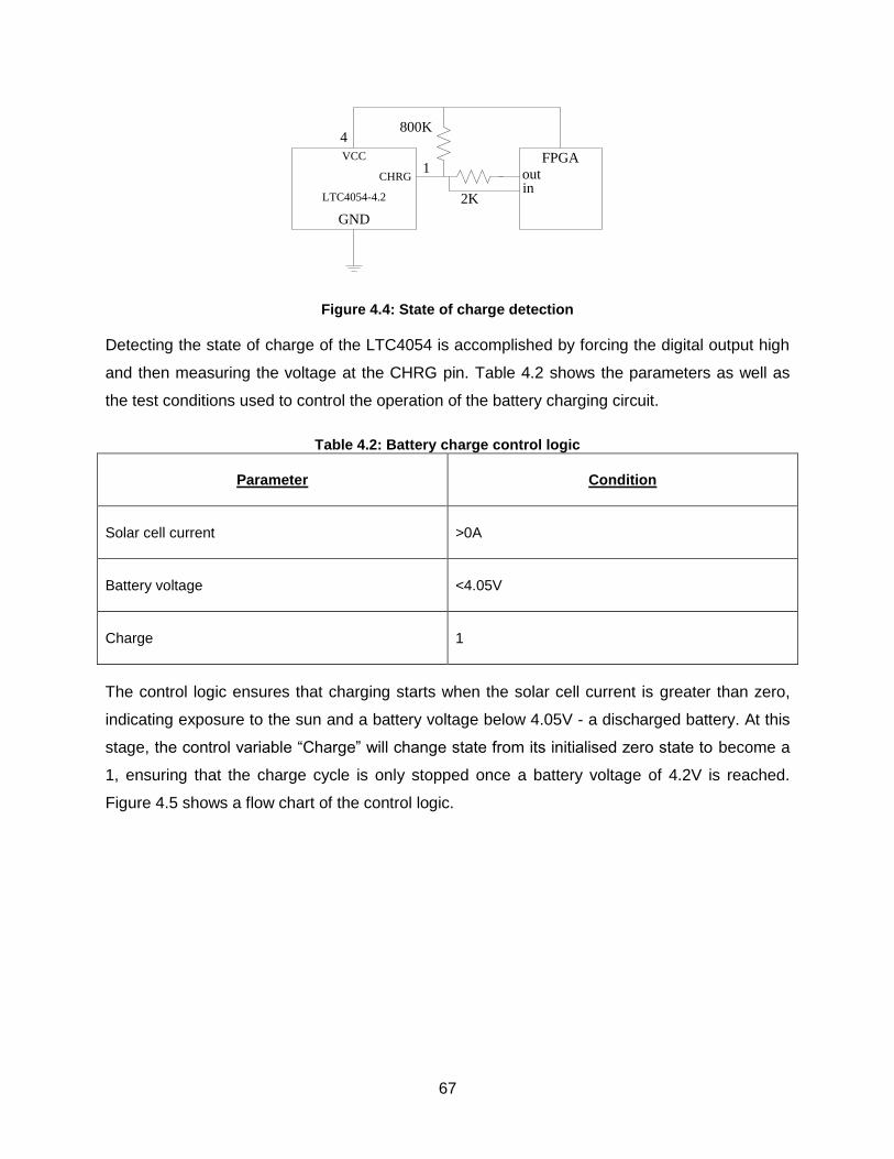
67
4
1
LTC4054-4.2
CHRG
VCC
GND
800K
2K
FPGAoutin
Figure 4.4: State of charge detection
Detecting the state of charge of the LTC4054 is accomplished by forcing the digital output high
and then measuring the voltage at the CHRG pin. Table 4.2 shows the parameters as well as
the test conditions used to control the operation of the battery charging circuit.
Table 4.2: Battery charge control logic
Parameter Condition
Solar cell current >0A
Battery voltage <4.05V
Charge 1
The control logic ensures that charging starts when the solar cell current is greater than zero,
indicating exposure to the sun and a battery voltage below 4.05V - a discharged battery. At this
stage, the control variable “Charge” will change state from its initialised zero state to become a
1, ensuring that the charge cycle is only stopped once a battery voltage of 4.2V is reached.
Figure 4.5 shows a flow chart of the control logic.

68
Start
Measure
1)Solar cell current
2)Battery voltage
Solar cell current > 0
&& Battery voltage <
4.05V or charge
Charge = 1
P&O MPPT
algorithm
Battery voltage
> 4.2V
Charge = 0
Yes
No
No
Yes
Figure 4.5: Battery charge algorithm
The LTC4054 continuously monitors the voltage at the BAT pin by using a comparator. The BAT
pin, pin 3 on the LTC4054-4.2, is connected to the lithium-ion battery providing the charge
current and regulating the voltage at 4.2V. The charge cycle automatically restarts when the
voltage falls below 4.05V which corresponds to approximately 10% depth-of discharge ensuring
the that secondary source of power is kept at or near its fully charged state, reducing the need
for longer charge cycles. The picture in Figure 4.6 shows the MPPT prototype.
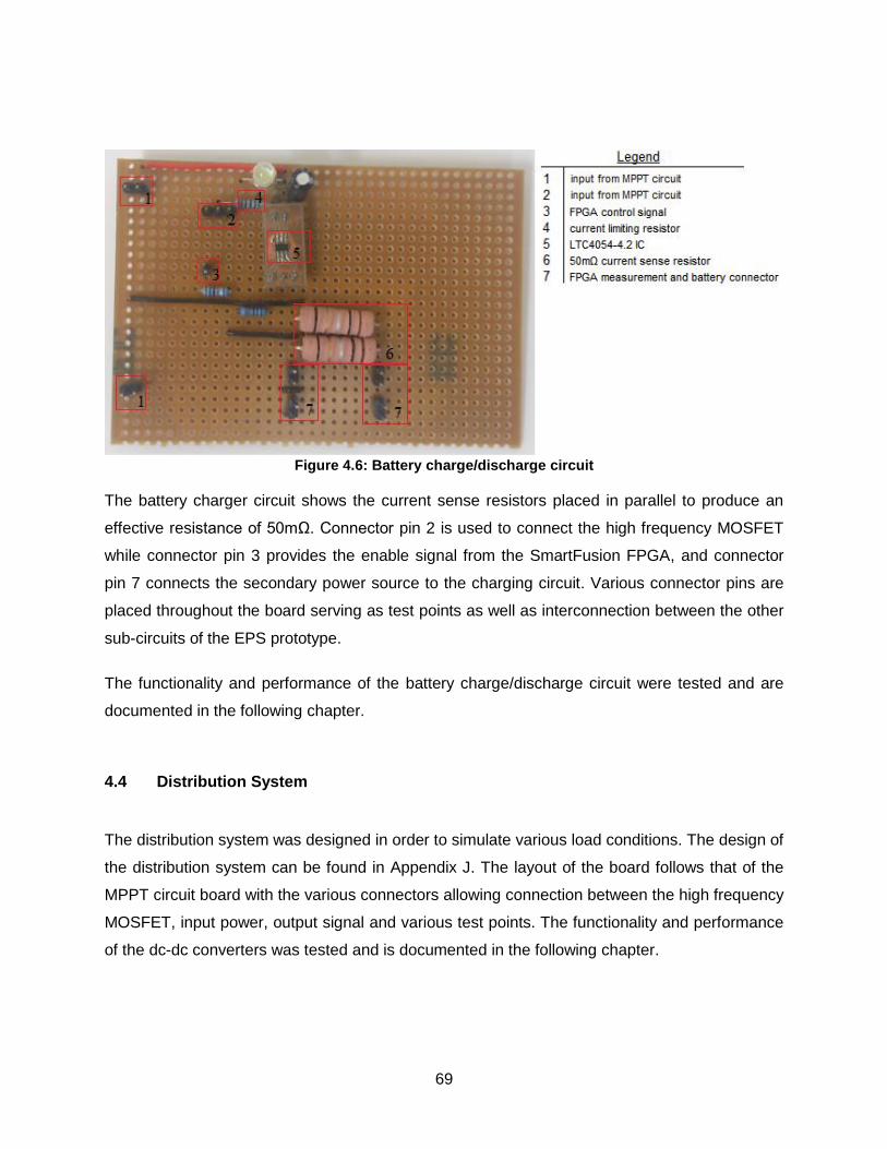
69
Figure 4.6: Battery charge/discharge circuit
The battery charger circuit shows the current sense resistors placed in parallel to produce an
effective resistance of 50mΩ. Connector pin 2 is used to connect the high frequency MOSFET
while connector pin 3 provides the enable signal from the SmartFusion FPGA, and connector
pin 7 connects the secondary power source to the charging circuit. Various connector pins are
placed throughout the board serving as test points as well as interconnection between the other
sub-circuits of the EPS prototype.
The functionality and performance of the battery charge/discharge circuit were tested and are
documented in the following chapter.
4.4 Distribution System
The distribution system was designed in order to simulate various load conditions. The design of
the distribution system can be found in Appendix J. The layout of the board follows that of the
MPPT circuit board with the various connectors allowing connection between the high frequency
MOSFET, input power, output signal and various test points. The functionality and performance
of the dc-dc converters was tested and is documented in the following chapter.
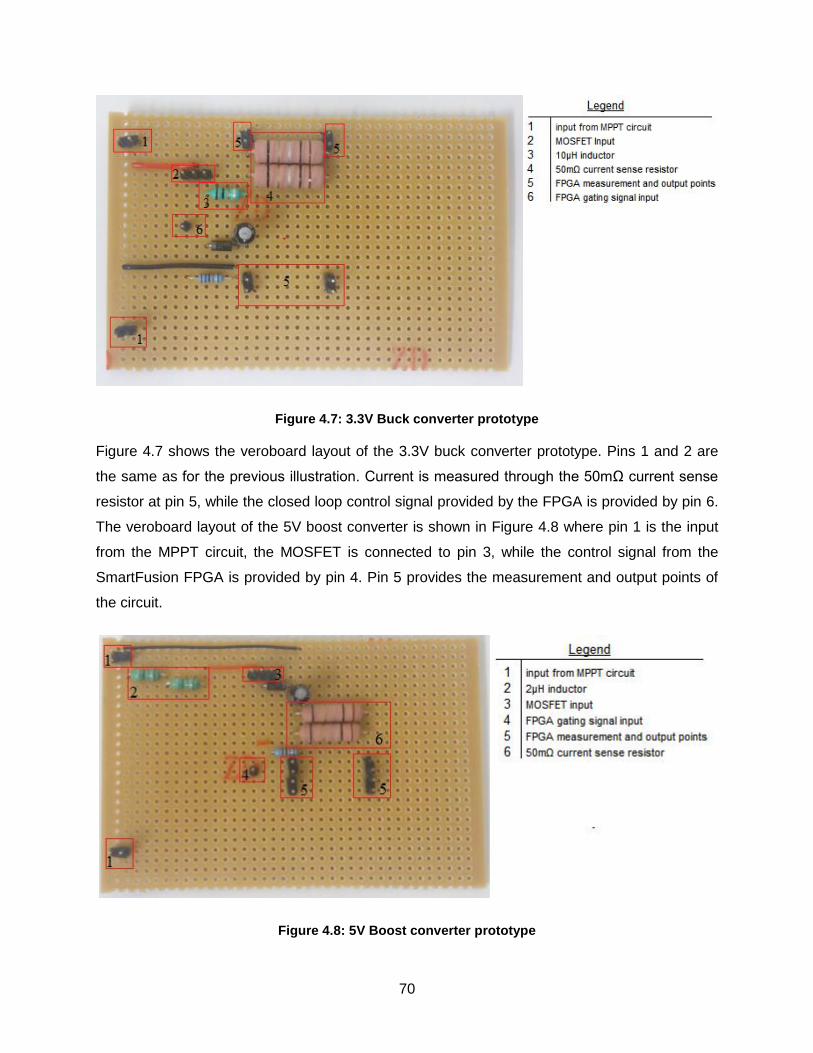
70
Figure 4.7: 3.3V Buck converter prototype
Figure 4.7 shows the veroboard layout of the 3.3V buck converter prototype. Pins 1 and 2 are
the same as for the previous illustration. Current is measured through the 50mΩ current sense
resistor at pin 5, while the closed loop control signal provided by the FPGA is provided by pin 6.
The veroboard layout of the 5V boost converter is shown in Figure 4.8 where pin 1 is the input
from the MPPT circuit, the MOSFET is connected to pin 3, while the control signal from the
SmartFusion FPGA is provided by pin 4. Pin 5 provides the measurement and output points of
the circuit.
Figure 4.8: 5V Boost converter prototype

71
4.5 Active Load
The active load, designed using the TIP122 Darlington pair power transistor, uses variable
resistors as indicated in Figure 4.9 to increase or decrease the current and thus cause a change
in power dissipation. Two of these active load circuits were designed and connected to the 3.3V
and 5V distribution busses. The active loads were tuned according Figure 3.13 and Figure 3.15
which illustrate the various resistance levels in order to dissipate 467.5mW and 472.5mW on the
3.3V bus and 5V bus respectively. Figure 4.10 shows the final prototype of the active load.
Figure 4.9: Active load circuit
Figure 4.10: Active load setup

72
4.6 FPGA
The SmartFusion FPGA is programmed using Libero®. The following major steps are executed
in order to programme the SmartFusion FPGA:
create the design;
implement the design;
programme the device; and
develop the firmware.
The bulk of the design layout is made during the ‘create design phase’ while the ‘implement
design phase’ is used to verify the design and undergo various design rule checks. Synthesis of
the design, test bench simulations and placing the various I/Os are also completed during this
phase. Programming the SmartFusion device is done using FlashPro where an .fdb file is
generated containing the hardware configuration of the FPGA. The firmware development
phase is used to write the application code which controls and directs the MSS, written in C or
C++. The following section addresses FPGA design implementation in more detail.
4.6.1 Creating Design
The smart design MSS is a graphical user interface (GUI) that contains a number of
representative peripheral images that are actually configurable software interfaces to determine
the functionality of the SmartFusion design. The MSS design canvas has different coloured
blocks: the blue blocks are for hardware configuration and the green blocks are not
configurable; and the grey blocks are disabled. Blocks that have a small check box can be
disabled to conserve FPGA resources and power. For this particular design application only the
UART_0 and ACE blocks are checked while all other check boxes are unchecked. If I2C
interfaces are required, these can be included in this step as they fall beyond the scope of this
document. Figure 4.11 shows the design canvas with the UART_0 and ACE block checked.

73
Figure 4.11: Smart design canvas
4.6.1.1 Clock Management
Figure 4.12: Clock configuration
Figure 4.12 shows the clock management configuration used in the design which can be found
in the top left corner of the MSS design canvas. The On-Chip RC oscillator was selected as the

74
clock input and the Phase Lock Loop (PLL) output of 30Mhz was selected. The ACLK, PCLK0,
PCLK1 and the FAB_CLK are divided by 1 to maintain the 30Mhz output frequency. FAB_CLK
is used as the input clock to the PWM module described later in this chapter. Once the system
clock is verified, the analogue compute engine (ACE) can be configured.
4.6.1.2 Analogue Compute Engine (ACE)
The ACE is configured by clicking the wrench icon illustrated in the smart design canvas as
shown in Figure 4.11. This user interface allows for the configuration of various analogue
inputs. This design requires the configuration of four Active Bipolar PreScalers (ABPS) and two
current monitors with a 12-bit resolution for increased accuracy. The ABPS senses the voltage
on an input pad and scales it to fit the range of the ADC which is between 0 - 2.56V. The design
is shown in Figure 4.13. An operational amplifier arranged in an inverted configuration with a
configurable feedback resistor and current source are able to provide four nominal gains and
offset ranges, of which the full range of +/- 15V was chosen for this design so as to allow
measurement over a large input range.
Figure 4.13: ABPS internal configuration
The voltages to be measured are the solar cell voltage, battery voltage, and the 3.3V and 5V
bus voltages. These voltages are applied as a negative feedback loop to provide closed loop
control in the converter design. Figure 4.14 shows the four ABPS used as well as their pin
assignments. These pin assignments were confirmed using the mixed signal daughter card user
guide.

75
Figure 4.14: ACE configuration
Monitoring the output current of the dc-dc converter used in the MPPT circuit is one of the
current monitors which can also be configured using the ACE. The second current monitor is
used to monitor the battery charge and discharge currents. The current monitors are
constructed from switched-capacitor circuits. This allows the current monitors to have a high
common mode input voltage range, a large common mode voltage rejection ratio, as well as
relatively high input impedance (Actel Corporation, 2010). The internal design (Figure 4.15)
shows that the high input signal (CM[n]_H) is attached to the CM[n] pad, low input signal
(CM[n]_L) is attached to the TM[n] pad. This is important as the current monitors are only able
to measure positive differential voltages indicating that CM[n]_H must be greater than CM[n]_L.
The current sensor uses an external current sense resistor of 0.05Ω, allowing current
measurements between 250uA and 1.02375A as suitable for the design application. Figure 4.14
shows that CM2 and TM2 are used to measure the battery charge and discharge voltage while
CM3 and TM3 are used to measure the output current of the MPPT circuit.
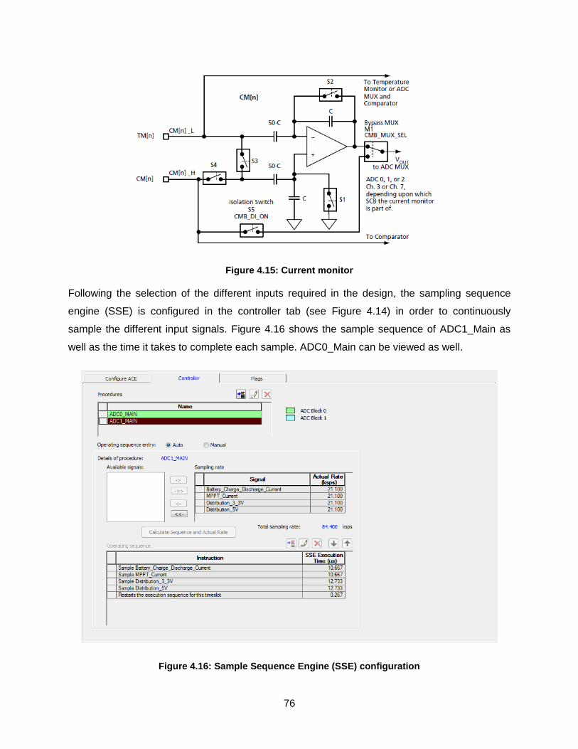
76
Figure 4.15: Current monitor
Following the selection of the different inputs required in the design, the sampling sequence
engine (SSE) is configured in the controller tab (see Figure 4.14) in order to continuously
sample the different input signals. Figure 4.16 shows the sample sequence of ADC1_Main as
well as the time it takes to complete each sample. ADC0_Main can be viewed as well.
Figure 4.16: Sample Sequence Engine (SSE) configuration
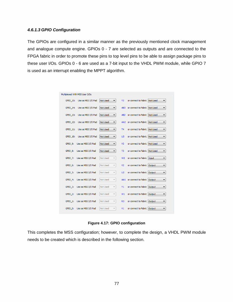
77
4.6.1.3 GPIO Configuration
The GPIOs are configured in a similar manner as the previously mentioned clock management
and analogue compute engine. GPIOs 0 - 7 are selected as outputs and are connected to the
FPGA fabric in order to promote these pins to top level pins to be able to assign package pins to
these user I/Os. GPIOs 0 - 6 are used as a 7-bit input to the VHDL PWM module, while GPIO 7
is used as an interrupt enabling the MPPT algorithm.
Figure 4.17: GPIO configuration
This completes the MSS configuration; however, to complete the design, a VHDL PWM module
needs to be created which is described in the following section.

78
4.6.1.4 VHDL PWM
The VHDL PWM is written using very-high-speed-integrated-circuit-hardware-description-
language (VHDL) which can be found in Appendix G. The VHDL component is generated under
the ‘create design’ tab in the design flow window and by selecting ‘create new HDL file’ option.
In the design hierarchy window, the HDL file is listed allowing for an HDL syntax check. Once
the syntax check has finished, the VHDL module can be instantiated into the MSS design
allowing the connection between the MSS and VDHL PWM module, as shown in Figure 4.18.
Figure 4.18: MSS and VHDL PWM
The VHDL PWM module is a 7-bit counter that counts to a value of 27-1 (127) and subsequently
restarts. The GPIOs 0 - 6 from the MSS outputs binary a value between 0 -127. The pwm_out
signal remains at a logic high for all values of the 7-bit pwm_value which are greater than the
counter value and switches to a logic low as soon as the pwm_value is less than the counter
value. This logic is confirmed through the implementation of a user test bench explained in the
following section.

79
4.6.1.5 VHDL Test Bench
The user test bench is written using VHDL and can be found in Appendix H. The test bench is
written in order to confirm the operation of the VHDL module. The test bench produces
simulated results by testing the operation of the module under various input conditions, as
illustrated in Figure 4.19. The conditions used to test this module involved the setting of the
pwm_value signal to represent different input signals from the MSS GPIOs in order to induce
changes in the pwm_out signal. The number of clock periods before a change in the state of the
pwm_value signal and the reset conditions were also set. The simulation runtime was set to
60µs.The test bench allowed the value from the MSS GPIOs to change from 0, 32, 64, 95 and
127, representing 0%, 25%, 50%, 75% and 100% duty cycles respectively.
4.6.2 Implement Design
The design implementation involves synthesis, place and route and also generating the
programming data. Synthesis performs a design rule check on the MSS design and allows the
process to continue if the VHDL components are successfully generated. Choosing to
interactively place and route the MSS design opens the Designer window which provides an
option for I/O attributor. This action should be performed before continuing with the FPGA layout
generation and the Flash Pro data generation.

80
Figure 4.19: Test bench output
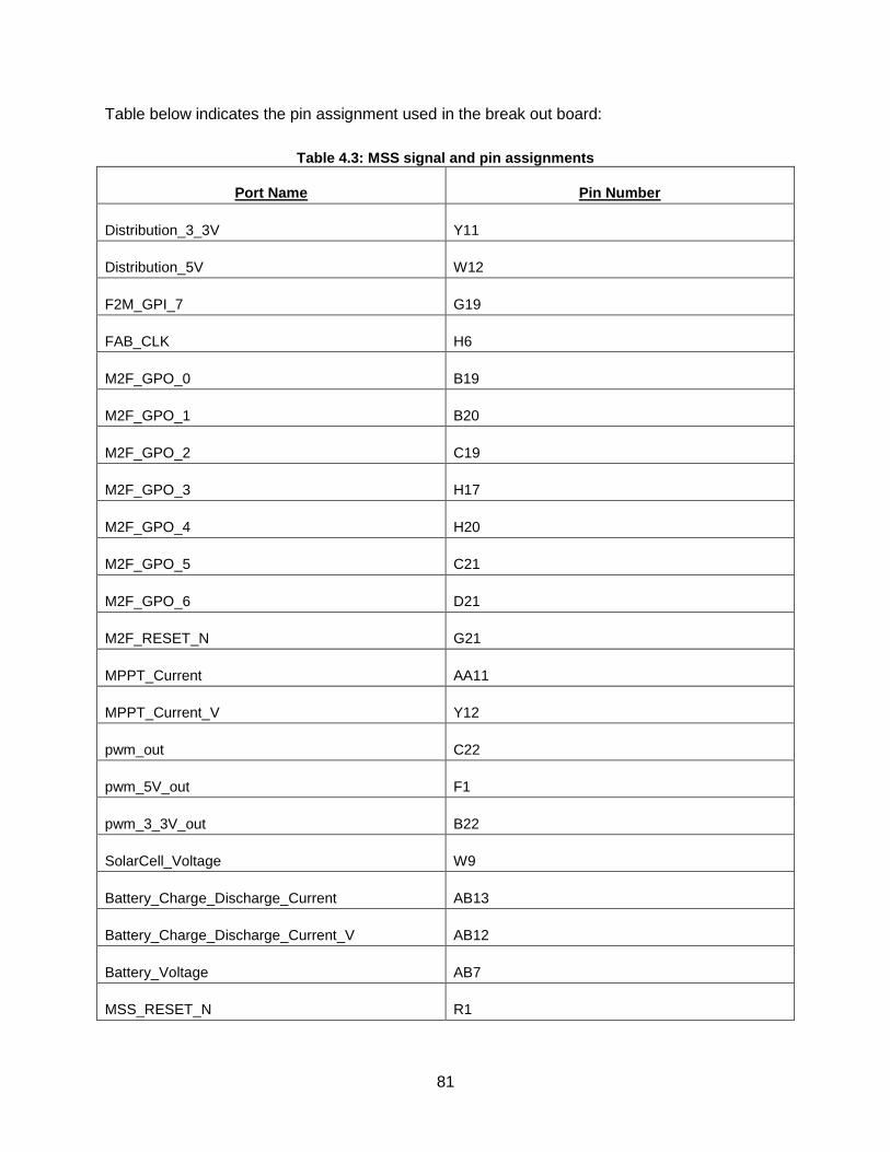
81
Table below indicates the pin assignment used in the break out board:
Table 4.3: MSS signal and pin assignments
Port Name Pin Number
Distribution_3_3V Y11
Distribution_5V W12
F2M_GPI_7 G19
FAB_CLK H6
M2F_GPO_0 B19
M2F_GPO_1 B20
M2F_GPO_2 C19
M2F_GPO_3 H17
M2F_GPO_4 H20
M2F_GPO_5 C21
M2F_GPO_6 D21
M2F_RESET_N G21
MPPT_Current AA11
MPPT_Current_V Y12
pwm_out C22
pwm_5V_out F1
pwm_3_3V_out B22
SolarCell_Voltage W9
Battery_Charge_Discharge_Current AB13
Battery_Charge_Discharge_Current_V AB12
Battery_Voltage AB7
MSS_RESET_N R1

82
The ‘commit and check’ option is used to confirm the pin and signal assignments, after which
the FPGA design layout and programming data can be generated.
4.6.3 Programming Device
The data files generated during the place and route procedure required for programming can be
accessed using FlashPro®. FlashPro® allows for the configuration of the device loading the .pdb
file onto the FPGA flash memory. The SmartFusion FPGA Eval-kit jumpers should be placed in
the correct positions to allow for FlashPro® programming.
4.6.4 Firmware Development
After the FPGA has been programmed, Softconsole® is used to write the application code used
in the firmware development phase.
HW Component
Start
SW Component
GPIO init
ADC init
UART init
Measure Voltage
Measure Current
Switch
Pressed
Duty Cycle = 8 %MPPT
Algorithm
Yes
No
Set Duty Cycle
gpio_output |= Duty_Cycle;
Start
PWM_value
PWM_value >
Count
Count++
count >
127
Count = 0
PWM_out =
‘1’
PWM_out =
‘0’
No
Yes
NoYes
Figure 4.20: Application code flowchart
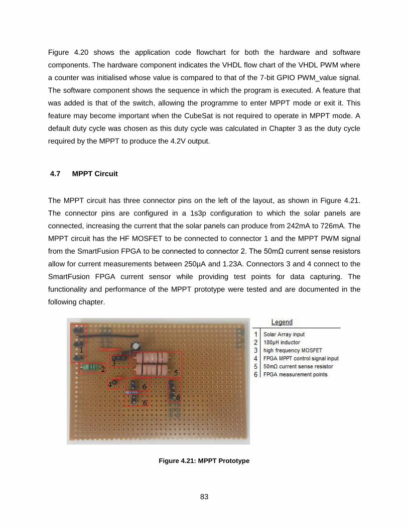
83
Figure 4.20 shows the application code flowchart for both the hardware and software
components. The hardware component indicates the VHDL flow chart of the VHDL PWM where
a counter was initialised whose value is compared to that of the 7-bit GPIO PWM_value signal.
The software component shows the sequence in which the program is executed. A feature that
was added is that of the switch, allowing the programme to enter MPPT mode or exit it. This
feature may become important when the CubeSat is not required to operate in MPPT mode. A
default duty cycle was chosen as this duty cycle was calculated in Chapter 3 as the duty cycle
required by the MPPT to produce the 4.2V output.
4.7 MPPT Circuit
The MPPT circuit has three connector pins on the left of the layout, as shown in Figure 4.21.
The connector pins are configured in a 1s3p configuration to which the solar panels are
connected, increasing the current that the solar panels can produce from 242mA to 726mA. The
MPPT circuit has the HF MOSFET to be connected to connector 1 and the MPPT PWM signal
from the SmartFusion FPGA to be connected to connector 2. The 50mΩ current sense resistors
allow for current measurements between 250µA and 1.23A. Connectors 3 and 4 connect to the
SmartFusion FPGA current sensor while providing test points for data capturing. The
functionality and performance of the MPPT prototype were tested and are documented in the
following chapter.
Figure 4.21: MPPT Prototype

84
Chapter 5
Prototype Evaluation and Tests Results
5.1 Prototype Overview
Figure 5.1: Electronic Power Supply (EPS) prototype
Various tests were conducted in order to verify the operation of the satellite power system using
the SmartFusion FPGA as the main controller. Figure 5.1 shows the interconnection of the
various EPS sub-circuit modules that were developed. Preliminary tests involved the verification
of the PWM output frequency, duty cycle verification, maximum power point tracking verification,
battery charging and discharging, as well as verification of operation of the distribution system.

85
Once these tests produced satisfactory results, a system integration test was conducted. Test
equipment included a Digital Multi-meter (DMM), DSO 1002A Oscilloscope, two N2863B low-
cost passive probes which provide10:1 attenuation and have an impedance of 10MΩ, and
connector leads from the mixed-signal daughter card to the circuit boards housing the different
modules of the EPS. An important aspect of testing was the calibration of the test probes as the
test probes have a certain reactance causing noise on the signal being measured. The probe
was calibrated and is shown in Figure 5.2. Another concern was the use of test leads as this
introduces noise within the system which can be viewed on the various output screens
presented as figures throughout this chapter.
Figure 5.2: Probe calibration
The test data was captured using the USB to UART interface and displayed using
HyperTerminal. The FPGA was programmed to communicate using the following settings
tabulated below:
Table 5.1: HyperTerminal port settings
Bits per seconds Data Bits Parity Stop Bits Flow Control
9600 8 None 1 None
A screen shot of the HyperTerminal output is illustrated in Figure 5.3. HyperTerminal was only
used as a method of data capturing and not intended for use on the satellite as the data on the
satellite is processed by the command and data handling sub-system. This data is sent using
I2C communication interface which can easily be included in the FPGA smart design. Data is
sent using a data string with the following format:
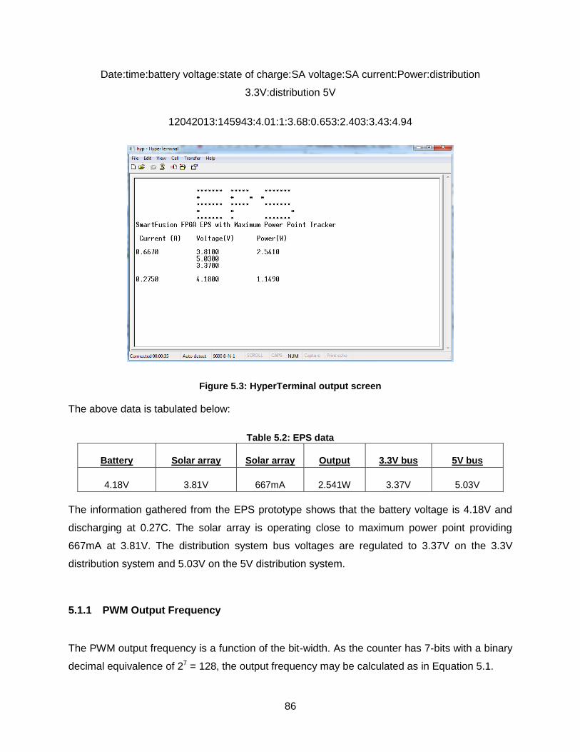
86
Date:time:battery voltage:state of charge:SA voltage:SA current:Power:distribution
3.3V:distribution 5V
12042013:145943:4.01:1:3.68:0.653:2.403:3.43:4.94
Figure 5.3: HyperTerminal output screen
The above data is tabulated below:
Table 5.2: EPS data
Battery voltage
Solar array voltage
Solar array Current
Output Power
3.3V bus voltage
5V bus voltage
4.18V 3.81V 667mA 2.541W 3.37V 5.03V
The information gathered from the EPS prototype shows that the battery voltage is 4.18V and
discharging at 0.27C. The solar array is operating close to maximum power point providing
667mA at 3.81V. The distribution system bus voltages are regulated to 3.37V on the 3.3V
distribution system and 5.03V on the 5V distribution system.
5.1.1 PWM Output Frequency
The PWM output frequency is a function of the bit-width. As the counter has 7-bits with a binary
decimal equivalence of 27 = 128, the output frequency may be calculated as in Equation 5.1.

87
128
clk_FabPWM Of
, (5.1)
128
30MhzPWM Of ,
kHzPWMOf 235 .
This step has certain significance as the dc-dc converters were designed using this frequency
shown in Appendix F and Appendix J.
Figure 5.4: Measured output frequency
Shown in Figure 5.4 is the output waveform of the PWM. The frequency was measured at
235kHz.
5.1.2 Duty Cycle Verification
The duty cycle verification test was conducted in order to ensure that the values programmed
into the GPIO output register produce the desired duty cycle. Figure 5.5 shows duty cycles of
25.7%, 50.2%, 74.8% and 100% at a frequency of 235 kHz. Exact duty cycles can be achieved;
however, this required the use of more GPIO inputs to increase the resolution of the PWM
circuit.
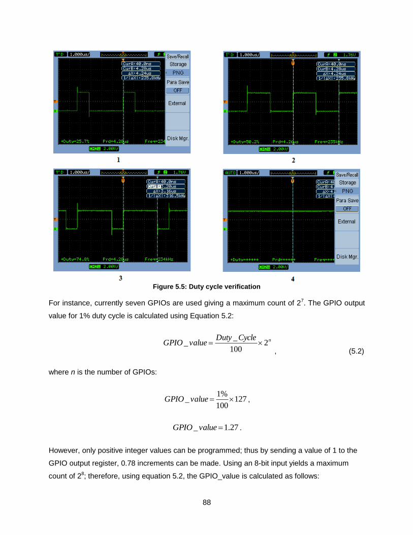
88
Figure 5.5: Duty cycle verification
For instance, currently seven GPIOs are used giving a maximum count of 27. The GPIO output
value for 1% duty cycle is calculated using Equation 5.2:
nCycleDutyvalueGPIO 2
100
__
, (5.2)
where n is the number of GPIOs:
127100
%1_ valueGPIO ,
27.1_ valueGPIO .
However, only positive integer values can be programmed; thus by sending a value of 1 to the
GPIO output register, 0.78 increments can be made. Using an 8-bit input yields a maximum
count of 28; therefore, using equation 5.2, the GPIO_value is calculated as follows:

89
255100
%1_ valueGPIO ,
55.2_ valueGPIO .
By sending a value of 2.55, 1% increments are possible; however, if a value of 1 is sent to the
GPIO output register, 0.38 increments are possible, thereby increasing the resolution of the
PWM output.
5.1.3 MPPT Verification
The experimental setup shown in Figure 5.6 determined the performance of the maximum point
tracking circuit. The solar cells were connected in a 1-series-3-parallel connection with the
active load tuned to 6Ω to draw maximum current. The sample sequencing engine is able to
take a MPPT current measurement every 47.067µs, as indicated in Figure 4.16. This indicates
that in order to achieve a time scale of 1000ms, 21246.308 samples need to be taken; however,
one sample was taken every 4ms and consequently only 250 samples were required to obtain a
1000ms time scale.
Figure 5.6: MPPT experimental setup

90
Figure 5.7: MPPT performance switching from low level to high level of solar irradiance
While the maximum power point tracking algorithm was not allowed to operate, approximately
200mA was drawn from the solar panels. Figure 5.7 indicates that at 310ms, the maximum
power point tracking algorithm was allowed to operate and an increase in solar cell output
current is evident. The output current increased from 200mA and fluctuated between 653mA
and 681mA. The input current at this moment was measured at 721mA, showing an efficiency
of 90.56% and 94.45%, a satisfactory result as power system efficiency of 76.5% was set as a
design requirement. The fluctuation is due to the perturbation around the maximum power point
which may be addressed by decreasing the size of the perturbation. The efficiency shows that
the maximum power point circuit dissipated 7% of the solar power available. The results indicate
that 194ms is required to determine the maximum power point when switching from a low level
of solar irradiance to a high level of solar irradiance while Figure 5.8 shows that 347ms is
required to move from a high level of solar irradiance to a low level of solar irradiance.
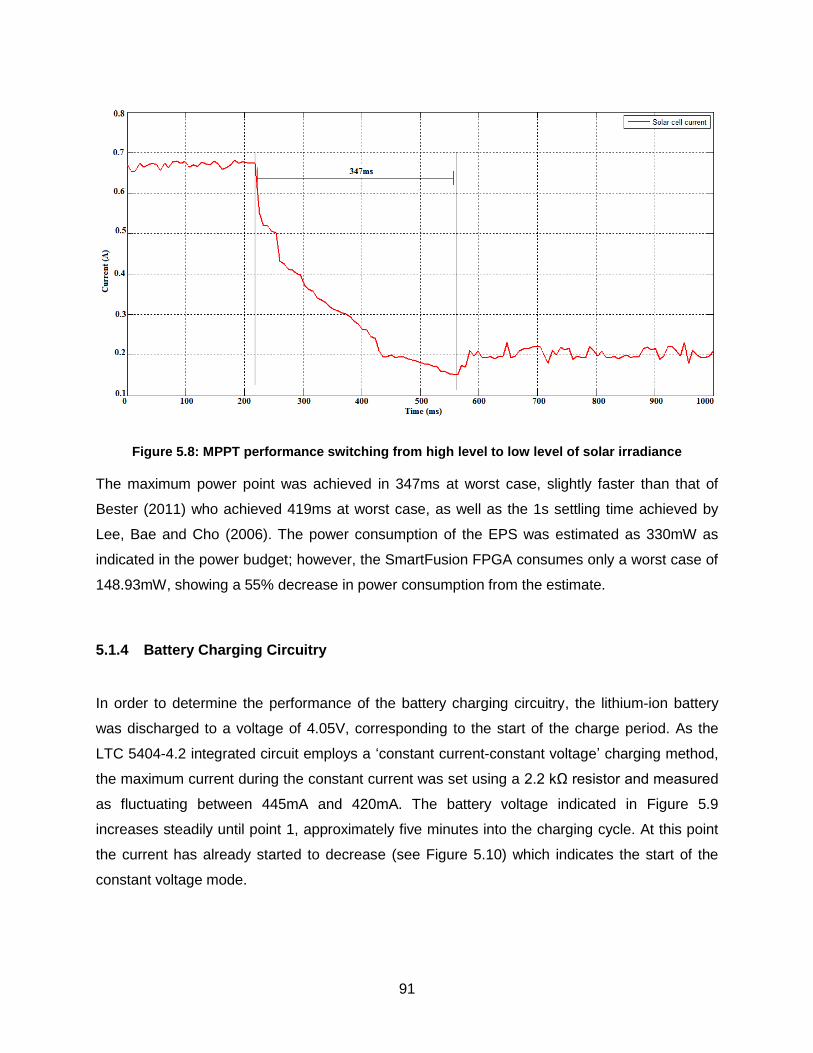
91
Figure 5.8: MPPT performance switching from high level to low level of solar irradiance
The maximum power point was achieved in 347ms at worst case, slightly faster than that of
Bester (2011) who achieved 419ms at worst case, as well as the 1s settling time achieved by
Lee, Bae and Cho (2006). The power consumption of the EPS was estimated as 330mW as
indicated in the power budget; however, the SmartFusion FPGA consumes only a worst case of
148.93mW, showing a 55% decrease in power consumption from the estimate.
5.1.4 Battery Charging Circuitry
In order to determine the performance of the battery charging circuitry, the lithium-ion battery
was discharged to a voltage of 4.05V, corresponding to the start of the charge period. As the
LTC 5404-4.2 integrated circuit employs a ‘constant current-constant voltage’ charging method,
the maximum current during the constant current was set using a 2.2 kΩ resistor and measured
as fluctuating between 445mA and 420mA. The battery voltage indicated in Figure 5.9
increases steadily until point 1, approximately five minutes into the charging cycle. At this point
the current has already started to decrease (see Figure 5.10) which indicates the start of the
constant voltage mode.

92
Figure 5.9: Battery voltage during charge period
Figure 5.10: Battery charge current during charge period
This is a satisfactory result as the completion of the charge cycle took approximately eight
minutes, less than the orbital time spent in the sun which was calculated to be 65.32min. A
concern might arise when the battery needs to discharge during the time spent in eclipse in
order to provide enough power to operate the transmitter. However, this concern will be
evaluated during the orbital simulation test.
5.1.5 Distribution System
The distribution system gating signal and duty cycles were verified and illustrated in Figure 5.11.
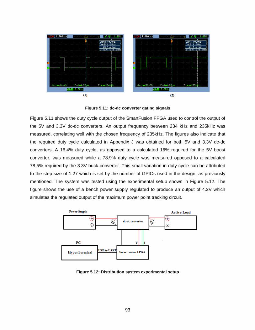
93
Figure 5.11: dc-dc converter gating signals
Figure 5.11 shows the duty cycle output of the SmartFusion FPGA used to control the output of
the 5V and 3.3V dc-dc converters. An output frequency between 234 kHz and 235kHz was
measured, correlating well with the chosen frequency of 235kHz. The figures also indicate that
the required duty cycle calculated in Appendix J was obtained for both 5V and 3.3V dc-dc
converters. A 16.4% duty cycle, as opposed to a calculated 16% required for the 5V boost
converter, was measured while a 78.9% duty cycle was measured opposed to a calculated
78.5% required by the 3.3V buck-converter. This small variation in duty cycle can be attributed
to the step size of 1.27 which is set by the number of GPIOs used in the design, as previously
mentioned. The system was tested using the experimental setup shown in Figure 5.12. The
figure shows the use of a bench power supply regulated to produce an output of 4.2V which
simulates the regulated output of the maximum power point tracking circuit.
Figure 5.12: Distribution system experimental setup
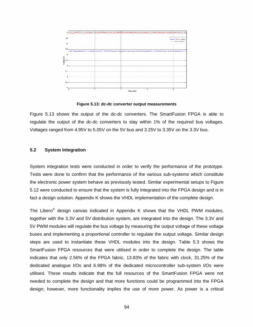
94
Figure 5.13: dc-dc converter output measurements
Figure 5.13 shows the output of the dc-dc converters. The SmartFusion FPGA is able to
regulate the output of the dc-dc converters to stay within 1% of the required bus voltages.
Voltages ranged from 4.95V to 5.05V on the 5V bus and 3.25V to 3.35V on the 3.3V bus.
5.2 System Integration
System integration tests were conducted in order to verify the performance of the prototype.
Tests were done to confirm that the performance of the various sub-systems which constitute
the electronic power system behave as previously tested. Similar experimental setups to Figure
5.12 were conducted to ensure that the system is fully integrated into the FPGA design and is in
fact a design solution. Appendix K shows the VHDL implementation of the complete design.
The Libero® design canvas indicated in Appendix K shows that the VHDL PWM modules,
together with the 3.3V and 5V distribution system, are integrated into the design. The 3.3V and
5V PWM modules will regulate the bus voltage by measuring the output voltage of these voltage
buses and implementing a proportional controller to regulate the output voltage. Similar design
steps are used to instantiate these VHDL modules into the design. Table 5.3 shows the
SmartFusion FPGA resources that were utilised in order to complete the design. The table
indicates that only 2.56% of the FPGA fabric, 13.83% of the fabric with clock, 31.25% of the
dedicated analogue I/Os and 6.98% of the dedicated microcontroller sub-system I/Os were
utilised. These results indicate that the full resources of the SmartFusion FPGA were not
needed to complete the design and that more functions could be programmed into the FPGA
design; however, more functionality implies the use of more power. As power is a critical
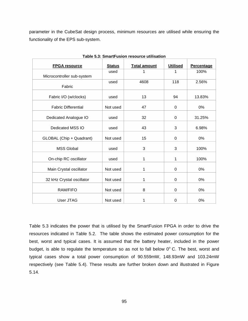
95
parameter in the CubeSat design process, minimum resources are utilised while ensuring the
functionality of the EPS sub-system.
Table 5.3: SmartFusion resource utilisation
Table 5.3 indicates the power that is utilised by the SmartFusion FPGA in order to drive the
resources indicated in Table 5.2. The table shows the estimated power consumption for the
best, worst and typical cases. It is assumed that the battery heater, included in the power
budget, is able to regulate the temperature so as not to fall below 0o C. The best, worst and
typical cases show a total power consumption of 90.559mW, 148.93mW and 103.24mW
respectively (see Table 5.4). These results are further broken down and illustrated in Figure
5.14.
FPGA resource
Status
Total amount
Utilised
Percentage
Microcontroller sub-system
used 1 1 100%
Fabric
used 4608 118 2.56%
Fabric I/O (w/clocks)
used
13
94
13.83%
Fabric Differential
Not used
47
0
0%
Dedicated Analogue IO
used
32
0
31.25%
Dedicated MSS IO
used
43
3
6.98%
GLOBAL (Chip + Quadrant)
Not used
15
0
0%
MSS Global
used
3
3
100%
On-chip RC oscillator
used
1
1
100%
Main Crystal oscillator
Not used
1
0
0%
32 kHz Crystal oscillator
Not used
1
0
0%
RAM/FIFO
Not used
8
0
0%
User JTAG
Not used
1
0
0%
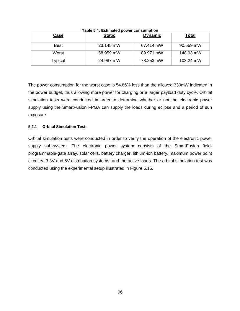
96
Table 5.4: Estimated power consumption
The power consumption for the worst case is 54.86% less than the allowed 330mW indicated in
the power budget, thus allowing more power for charging or a larger payload duty cycle. Orbital
simulation tests were conducted in order to determine whether or not the electronic power
supply using the SmartFusion FPGA can supply the loads during eclipse and a period of sun
exposure.
5.2.1 Orbital Simulation Tests
Orbital simulation tests were conducted in order to verify the operation of the electronic power
supply sub-system. The electronic power system consists of the SmartFusion field-
programmable-gate array, solar cells, battery charger, lithium-ion battery, maximum power point
circuitry, 3.3V and 5V distribution systems, and the active loads. The orbital simulation test was
conducted using the experimental setup illustrated in Figure 5.15.
Case
Static Dynamic Total
Best 23.145 mW 67.414 mW 90.559 mW
Worst 58.959 mW 89.971 mW 148.93 mW
Typical 24.987 mW 78.253 mW 103.24 mW

97
Figure 5.14: SmartFusion FPGA power consumption
Figure 5.15: Orbital simulation configuration
Figure 5.15 shows two experimental configurations for simulating the CubeSat power
configuration during the period of exposure to the sun, indicated by 1. Configuration 2 shows the
configuration during the period of eclipse.
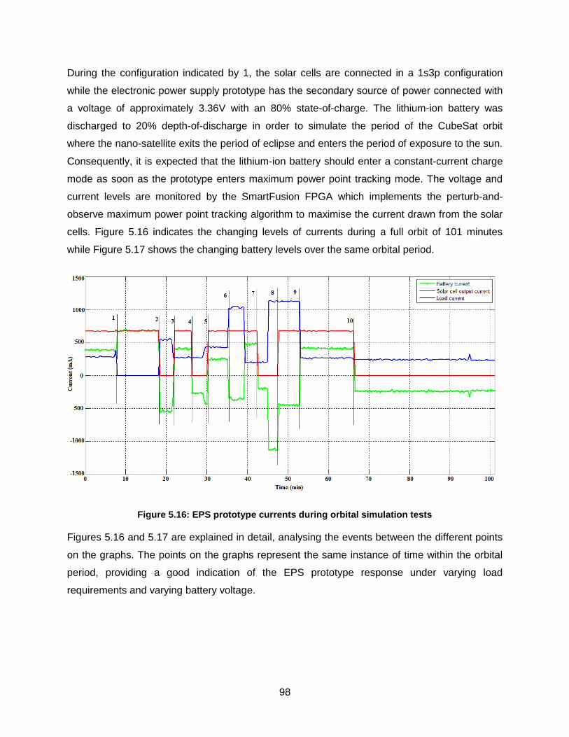
98
During the configuration indicated by 1, the solar cells are connected in a 1s3p configuration
while the electronic power supply prototype has the secondary source of power connected with
a voltage of approximately 3.36V with an 80% state-of-charge. The lithium-ion battery was
discharged to 20% depth-of-discharge in order to simulate the period of the CubeSat orbit
where the nano-satellite exits the period of eclipse and enters the period of exposure to the sun.
Consequently, it is expected that the lithium-ion battery should enter a constant-current charge
mode as soon as the prototype enters maximum power point tracking mode. The voltage and
current levels are monitored by the SmartFusion FPGA which implements the perturb-and-
observe maximum power point tracking algorithm to maximise the current drawn from the solar
cells. Figure 5.16 indicates the changing levels of currents during a full orbit of 101 minutes
while Figure 5.17 shows the changing battery levels over the same orbital period.
Figure 5.16: EPS prototype currents during orbital simulation tests
Figures 5.16 and 5.17 are explained in detail, analysing the events between the different points
on the graphs. The points on the graphs represent the same instance of time within the orbital
period, providing a good indication of the EPS prototype response under varying load
requirements and varying battery voltage.

99
From point 0 to point 1:
The EPS prototype is operating with the maximum power point tracker enabled simulating the
period of sun exposure. The solar cells are able to obtain a maximum power point and supply
the CubeSat with approximately 0.668mA, indicated by the red data points. This current varies
due the perturbations that occur around the maximum power point. The blue data points
indicate that the current drawn by the load is less than the current produced at maximum power,
allowing the lithium-ion battery to charge. The charge period increases the state-of-charge of
the lithium-ion battery indicated in Figure 5.17 between point 0 and point 2.
Figure 5.17: Battery voltage variation
From point 1 to point 2:
It is noticed that as soon as the load current is decreased to 0A, the currents produced by the
solar cells are used to charge the secondary power source at a faster rate indicated between
point 1 and point 2, shown in Figure 5.17. Previous versions of this prototype were unable to
source all the current into the battery due to the 2.2kΩ program resistor (RPROG) of the battery
charging circuit; however, the problem was solved by replacing this resistor with a 1.2kΩ
resistor allowing more current to be sourced by the charging circuit.

100
From point 2 to point 3:
The MPPT was terminated due the state-of-charge of the lithium-ion battery being 100% at
which point the battery immediately enters a state-of-discharge shown by the negative current
which matches the requirements of the load. The battery voltage was allowed to drop to 4.05V
before activating the MPPT algorithm again (this value can be changed via software).
From point 3 to point 4:
For the period between point 3 and point 4, the secondary source of power was allowed to
charge while the solar cells were able to supply a load current of 275mA. 4.2V was reached at
point 4, stopping the charge cycle and thus the operation of the maximum power point tracking
algorithm.
From point 4 to point 7:
The maximum power point tracking algorithm was restarted at point 5 when the battery voltage
dropped below 4.05V and then activated the charging cycle. At point 6 the load current was
increased to 1000mA, which is higher than the current the solar cells are able to produce. The
lithium-ion battery voltage decreased at point 6 in Figure 5.17 indicating that that the battery had
entered a state of discharge and thus supplying the balance of the current required by the load.
As soon as the load current was decreased, the battery started charging again until the battery
voltage reached 4.2V at point 7.
From point 7 to point 9:
From point 7, a load current of 275mA was supplied by the battery before a large current of
1100mA was drawn. The battery voltage dropped to below 4.05V which activated the maximum
power point tracking algorithm; however, the battery continued to discharge as the load current
of 1100mA was maintained for another three minutes during which the battery voltage dropped
to 3.72V.
From point 9 to 10 minutes:
At point 9 normal operations continued until point 10, allowing the battery to be fully charged
before entering the simulated eclipse period indicated by the zero solar cell output current after
point 10. The battery continues to discharge until 3.55V, approximately 85% state-of-charge

101
with a depth-of-discharge of 15%, higher than the calculated 13.8% DoD. However, the 13.8%
was calculated at a discharge current of 236.2mAh while the orbital simulation showed current
drawn to be approximately 275mAh, giving rise to the slight variation.
The orbital simulation tests produced satisfactory results as they show that the secondary
sources of power are able to overcome the eclipse period through the implementation of the
SmartFusion FPGA as the main controller.

102
Chapter 6
Conclusion and Recommendations
6.1 Conclusion
The research aimed to investigate the use of a field-programmable-gate-array as the main
controller in an electronic power system of a nano-satellite. Field-programmable-gate-arrays
have not yet been implemented on CubeSat electronic power supply sub-systems because the
perception is that these devices consume relatively large amounts of power. Because the size,
weight and power constraints of CubeSats are limiting factors of the CubeSat standard,
engineers and researchers are endeavouring to overcome these constraints by eliminating the
need for larger more expensive satellites. Thus, addressing the size, weight and power
constraints of individual sub-systems that constitute the CubeSat will not only increase the
efficiency of that particular sub-system but increase the efficiency of the entire CubeSat. The
research investigated whether or not the implementation of a FPGA-based electronic power
supply sub-system addresses these identified size, weight and power constraints.
The electronic power system using the SmartFusion FPGA as the main controller prototype was
designed, developed and tested. The various steps taken to complete the project are listed
below:
• Power budget was designed considering the environment in space, orbital parameters,
critical sub-systems, payloads and the duty cycle of operation of these sub-systems.
• Solar cell technology was investigated and an appropriate maximum power point
tracking algorithm was selected from comparative studies.
• A secondary source of power was sized according to the system requirements.
• An electronic power supply prototype was designed and developed with the Smart-
Fusion FPGA as the main controller of the nano-satellite.

103
• Stand-alone tests were conducted to verify the operation of the different sub-circuits of
the EPS sub-system.
• Orbital simulation tests were conducted to verify the integration of the various sub-
circuits of the sub-system.
The SmartFusion FPGA was programmed with the necessary control algorithms in order to
control the state of charge of the lithium-ion battery. The FPGA employs a maximum power
point tracking algorithm that is able to track the change in maximum power due to the variations
in solar irradiance. The EPS prototype is also able to deal with variations in load current while
being able to charge the secondary source of power during the full period of sun exposure.
During the eclipse period, the battery voltage decreased to 3.55V, corresponding to an
approximate 15% depth-of-discharge, falling into a satisfactory region as a 20% depth-of
discharge was anticipated during the eclipse period.
The SmartFusion FPGA offers a high level of integration as it contain ADCs, an ACE, SSE and
PPE, decreasing the component count of non-FPGA control based nano-satellite power
systems. The aforementioned features optimise the EPS-system even more as the SSE
captures the information from the ACE and passes it to the PPE where the data can be
transformed and filtered. These actions ensure that during high microcontroller activity, sample
sequencing occurs and information required for calculating the MPPT is not lost, thereby
improving the reliability of the system.
To limit the power consumption of the FPGA, the full functionality of the FPGA was not utilised.
The SmartFusion FPGA analogue compute engine allows for complex algorithms such as the
maximum power point tracking and battery charge regulation algorithm to be implemented on
the microcontroller sub-system, as these allow for the offloading of many repetitive calculations
which then allow the microcontroller sub-system to perform functions with higher accuracy and
increased performance. These unique features of the SmartFusion FPGA address the size,
weight and power constraints of the CubeSat standard within the electronic power supply sub-
system.
6.2 Problems Encountered
SoftConsole does not enter debug mode when frequencies less than 8Mhz is chosen.

104
D13 (red LED) on the SmartFusion lights up and loads the last pdb. file in the NVM. This
was due to faulty CP210x USB to UART driver (re-install driver to fix problem).
Current sense resistor. Value ranges from 0.00001Ω to 0.1Ω. A 0.01Ω resistor was
placed in parallel with another 0.01Ω resistor to achieve a 0.005Ω current sense resistor,
allowing a measurement range between 250uA and 1.023A.
CorePWM driver did not load. When using the CorePWM module, the APB3 AMBA
should be used in conjunction because the CorePWM will be connected as the slave
while interfacing with this AMBA.
Make file not generated. This problem was solved by creating a make file in which the
files are generated. The cmd line: “taskkill /IM make.exe /F” was used to terminate
hanging make file instances.
Remember to include all .h files.
CorePWM implementation did not work.
The PWM 1 and PWM 0 pins have a first order RC filter connected on their output which
could filter certain frequencies causing a 0V output when measured using an
oscilloscope.
6.3 Recommendations for Future Work
Using the mixed signal daughter card only allowed the use of two of the four available
current sensors, limiting the amount of information that could be gathered at a single
instance of time; however, using the SmartFusion FPGA as a stand-alone device will
allow the utilisation of the resources as dedicated evaluation board pin outs become
available.
Using the FPGA in a system with more power available will allow the usage of more of
the available SmartFusion capacity as only 31.25% of the FPGA’s analogue resources,
6.98% MSS I/O resources and only 2.56% of the FPGA fabric were used to complete the
design. Therefore, developing an EPS with an integrated OBC, communication,
command and data handling or payload sub-system will utilise more of the SmartFusion
functionalities and produce a system with lower component count and smaller footprint.
Thus, various levels of redundancy can be programmed into the eNVM and only become
active if a component or sub-system should fail, further augmenting the nano-satellite
through the use of the SmartFusion FPGA.

105
This design could be implemented on a PC-104 circuit board and could make use of
surface mount components. Using the surface mount components will further reduce the
physical size of the EPS sub-system on PC-104 circuit board while a good PCB design
and layout reduce the noise signals that were superimposed on the various output and
control signals. This space saved can be used for redundant circuits, further increasing
the reliability of the system.
Publications emanating from the dissertation
Cupido, S.W.J., Adonis, M. & Barnard, A. (in-press). MPPT efficacy design via an FPGA
implementation for Nano-satellites, International Journal on Energy Conversion (IRECON).
Cupido, S.W.J. & Adonis, M. (in-press). MPPT algorithm via VHDL programming for a CubeSat,
ICEE/ICIT-2013, 8 to 12 December 2013 in Cape Town, South Africa

106
References
Actel Corporation. 2010. Actel SmartFusion Programmable Analogue user guide.
www.microsemi.com/soc/documents/SmartFusion_Analog_UG.pdf [viewed 4 February 2012 ].
Akagi, J. M. n.d. Power generation and distribution system design for the leonidas cubesat
network. http://www.spacegrant.hawaii.edu/reports/15_FA05-SP06/Akagi_Justin_FA.pdf
[viewed 6 January 2012].
Altera, n.d. Alter FPGAs, http://www.altera.com/devices/fpga/fpga-index.html viewed [viewed 11
August 2011].
Anon. 2011. ESA Cubs delivered for first Vega flight. Esa education: 14 November.
http://www.esa.int/SPECIALS/Education/SEM3L0WWVUG_0.html [viewed 14 November 2011].
Arnold, S., Nuzzaci, R. & Gordon-Ross, A. 2012. Energy Budgeting for CubeSats with an
Integrated FPGA. IEEE. http://www.ann.ece.ufl.edu/pubs_and_talks/Aero12_arnold_ERB.pdf .
[viewed 18 May 2012 ].
Bester, J.E. 2011. Electrical Power System for a CubeSat Nano-Satellite. Unpublished Master’s
Thesis, Cape Peninsula University of Technology, Bellville.
Clark, C. & Hall, K. 2002. Power system design and performance on the world’s most advanced
in-orbit nano-satellite. In Wilson, A (ed). Proceedings of the sixth European Space Power
Conference. Netherlands: ESA: 129-134.
Clark, C. & Simon, E. 2007. Evaluation of lithium polymer technology for small satellite
applications. Proceedings of the 21st Annual AIAA/USU Conference on Small Satellites. Logan,
UT: Utah State University Research Foundation. [ Published on CD-ROM].
Clark, C. & Logan, R. 2011. Power Budgets for CubeSat Mission Success. PowerPoint
presentation. http://www.clyde-space.com/documents/2276 [viewed. 14 April 2012].
Clyde Space. 2010. URL http://www.clyde-space.com/ [viewed 14 April 2012].
Connection. 2011. Photoelectric effect, The Photoelectric effect.
http://cnx.org/content/m39551/1.1/?collection=col11244/latest [viewed 18 May 2012].

107
Danionics. n.d. Datasheet: product specification-DLP485586G3.
Davide, A. n.d. White Paper on Exploring issues relating to Li-Ion cells and batteries, viewed
June 2012. http://liionbms.com/php/white_papers.php.
Dearborn, S. 2004. Power management in portable applications: Charging lithium ion/polymer
batteries. Microchip Technology Inc..
http://ww1.microchip.com/downloads/en/AppNotes/00947a.pdf [viewed 18 May 2012].
Emcore. 2004. Datasheet: 27.5 % Advanced triple-junction (AJT) High Efficiency Solar Cells for
Space Applications.
Emcore. 2006. Datasheet: 28.5 % BTJ Triple-Junction High Efficiency Solar Cells for Space
Applications.
Enertech International. 2007. Specification of product: rechargeable Li-ion polymer battery
model: SPB9345136UH1 (4.4Ah).
GomSpace. 2012. Nano-Power P-Series datasheet. http://gomspace.com/documents/GS-DS-
NANOPOWER-3.0.7.pdf [viewed 30 June 2012].
González-Longatt, F.M. 2005. Model of Photovoltaic Module in MatlabTM . 2do Congreso
Iberoamericano de Estudiantes de Ingeniería Eléctrica, Electrónica y Computación (II CIBELEC
2005). Puerto la Cruz, Venezuela.
Greenwald, R. A., Baker, K. B., Dudeney, J. R., Pinnock, M., Jones, T. B., Thomas, E. C.,
Villain, J. P., Cerisier, J. C., Senior, C., Hanuise, C., Hunsucker, R. D., Sofko, G., Koehler, J.,
Nielsen, E., Hamill, D. C., & Krein, T. P. 1999. A Zero Ripple Technique Applicable to Any DC
Converter, IEEE Power Electronics Specialists Conference, 1165-1171.
Harjai, A., Bhardwaj, A. & Sandhibigraha, M. 2010. Study of Maximum Power Point Tracking
(MPPT) Techniques in a Solar Photovoltaic Array. Unpublished Thesis, National Institute of
Technology, Rourkela.
Hohm, D.P. & Ropp, M.E. 2000. Comparative study of maximum power point tracking
algorithms using an experimental, programmable, maximum power point tracking test bed,

108
Photovoltaic Specialists Conference, 2000. Conference Record of the Twenty-Eighth
IEEE:1699-1702.
Horner, M. 2011. ‘Photoelectric effect’, Connections.
http://cnx.org/content/m39551/1.1/?collection=col11244/latest [viewed 25 September 2011].
International Astronautical Congress. 2011. French South African Institute of Technology.
http://iac2011.com/space-south-africa/fsati [viewed 23 August 2011].
Kjaer, S. 2002. ‘CubeSat Power Systems’, PowerPoint presentation.
http://www.control.auc.dk/~raf/Aerospace/CUBESAT.pdf [viewed 13 February 2012].
Lee, J., Bae, H. & Cho, B. 2006. Advanced incremental conductance MPPT algorithm with a
variable step size. Proceedings of the 12th International Power Electronics and Motion Control
Conference (EPE-PEMC '06). New York, NY: IEEE: 603-607.
Linear Technology, 2010. LTC4054-4.2/LTC4054X-4.2: Standalone Linear Li-Ion Battery
Charger with Thermal Regulation in Thin SOT, datasheet.
http://cds.linear.com/docs/Datasheet/405442xf.pdf [viewed 18 June 2012].
Maini, A. & Agrawal, V. 2007. Satellite technology: principles and applications. West Sussex:
Wiley: 134-140.
McLaren, V., Clark, C., Simon, E. & Hendel, B. 2008. Lithium ion polymer cell for small satellite.
Paper presented at the 2008 NASA Aerospace Battery Workshop.
Mellit, A., Rezzouk, H., Messai, A. & Medjahed, B. 2010. FPGA-Based real time implementation
of MPPT-controller for photovoltaic systems. Renewable Energy: an International Journal.
http://www.elsevier.com/locate/rener [viewed 19 February 2012].
Microchip. 2004. Application note AN947. Power management in portable applications: charging
lithium ion / lithium polymer batteries.
Microsemi SoC Product Group. 2011. Terrestrial FPGA and SoC Product Catalog - Actel.
http://www.actel.com/documents/ProdCat_PIB.pdf [viewed 13 February 2012].
Microsemi SoC Product Group. 2012. SmartFusion Customizable System-on-Chip (cSoC).
http://www.actel.com/documents/SmartFusion_DS.PDF [viewed 13 April 2012].

109
Microsemi SoC Product Group. 2012. SmartFusion cSoC: System Power Optimization using
low Power Modes. [13 April 2012].
Nason, I., Creedon, M .& Johansen, N. 2002. CubeSat P-Pod Deployer Requirements.
http://www.oh1sa.net/data/satellite/cubesat/P-POD-mk1/ppod_mk1_icd.pdf [viewed 1 February
2012].
Neeraj, M., Neethu, K.T., Nikhil, V., & Nirmaldev, M.R. 2012. Photovoltaic water pumping
system with maximum power point tracking. Unpublished Thesis, Government Engineering
College, Thissur. (Paper sent by author).
Oi, A. 2005. Design and Simulation of a photovoltaic water pumping system. Master’s Thesis,
California Polytechnic State University, Pomona.
http://courseware.ee.calpoly.edu/~jharris/research/super_project/ao_thesis.pdf. [viewed 20 July
2012].
Person,T.E. 2004. FPGA-based design of a maximum power point tracking system for space
applications. Unpublished Master’s thesis, University of Central Florida, Orlando.
Ping, W., Hui, D., Changyu, D. & Shengbiao, Q. 2011. "An improved MPPT algorithm based on
traditional incremental conductance method," Power Electronics Systems and Applications
(PESA), 2011 4th International Conference: 1-4, 8-10, June.
201 http://ieeexplore.ieee.org/stamp/stamp.jsp?tp=&arnumber=5982914&isnumber=5982872
[viewed 11 June 2012].
Simpson, C. n.d. Texas Instrument datasheet, Battery charging, viewed June 2012.
http://www.ti.com/lit/an/snva557/snva557.pdf.
Singh, C.P. and Kaushal, N. 2008. Design of an FPGA-Based Lithium-Ion Battery charger
system. Unpublished Thesis, National Institute of Technology, Rourkela.
Snyman, D. & Enslin, J. 1993. Simplified maximum power point controller for PV installations.
Conference Record of the 23rd IEEE Photovoltaic Specialist Conference (PVSC ’93). New York,
NY:IEEE 1240-1245.
Solar Direct Technologies. 2009. Datasheet: SDT003.
Solar Direct Technologies. 2009. Datasheet: SDT100.

110
Spectrolab. 2010. Datasheet: 28.3% ultra-triple junction (UTJ) solar cells.
Spectrolab. 2010. Datasheet: 29.5% next-triple junction (XJT) solar cells.
Sree, B.M., Ramaprabha, R. & Mathur, B.L. 2011. Design and Modelling of Standalone Solar
Photovoltaic Charging System. International Journal of Computer Applications, 18.
Sunica. n.d. Sunica Ni-Cd battery Technical manual, viewed January 2012.
http://www.mrl.nott.ac.uk/~mbf/antarctica/files/tm_sun.pdf.
Walker, G. 2001. Evaluating MPPT converter topologies using a MATLAB PV model. J. Elect.
Electron. Eng. Australia, 21: 49–56, 2001.
Waydo, S.,Henry, D. & Campbell, M. 2002. CubeSat design for LEO-based Earth science
missions, Aerospace Conference Proceedings. IEEE, 1:1-445.
http://ieeexplore.ieee.org/stamp/stamp.jsp?tp=&arnumber=1036863&isnumber=22238 [viewed
11 August 2011].
Wu, W., Pongratananukul, N., Qiu, W., Rustom, K., Kasparis, T., & Batarseh, I. 2003. DSP-
based multiple peak power tracking for expandable power system. Applied Power
Electronics Conference and Exposition.
Xilinx, n.d. ‘All Programmable FPGAs’, viewed August.
2011http://www.xilinx.com/products/silicon-devices/fpga/index.htm.
Yi-Hsin Weng; Hui-Wen Tsai; Ming-Dou Ker, Design of charge pump circuit in low-voltage
CMOS process with suppressed return-back leakage current. IC Design and Technology
(ICICDT), 2010 IEEE International Conference:155,158. 2-4 June 2010.
Yi-Hwa, L., Jen-Chung, L. & Jen-Hao, T. 2004. An FPGA-based lithium-ion battery charger
system, TENCON 2004 IEEE Region 10 Conference, D: 435- 438 and 4: 21-24.
Yi-Hwa, L. & Jen-Hao, T. 2006. Design and Implementation of a Fully-digital Lithium-Ion Battery
Charger. TENCON 2006 IEEE Region 10 Conference. Taiwan Univ. of Sci. & Technol., Taipei
14-17 Nov. 2006:1- 4.

111
Appendix A: Nano-Satellite Mission
Table A-1: Previous CubeSat missions
Country Year CubeSat name
South Africa 2012 ZA-CUBE 01
Romania 2012 GOLIAT
Poland 2012 BPW-Sat
France 2012 Robusta
Spain 2012 XaTcobea
Hungary 2012 MaSat-1

112
Appendix B: MATLAB® Source Code
V-I characteristics
Iph = 3.17;
Isat = 0.5*(10^-6);
q = 1.6*(10^-19); %Electron Charge
k =1.38*(10^-23); % Boltzmann's constant
n =1.5; %diode ideality factor
Ns =36; %series connected cell
Rs = 0.004; %series resistance
Vd = 0.1:21.8;
Ta=20; %Reference temperature
Tcell = 273+Ta;
I = Iph-Isat*(exp((q*Vd)/(n*k*Tcell*Ns))-1)
V = Vd-I*Rs
figure;
plot(V,I,'k')
hold on
Tcell = 273+Ta;
I = Iph-Isat*(exp((q*Vd)/(n*k*Tcell*Ns))-1)
V = Vd-I*Rs
%figure;
plot(V,I,'r')
Ta=40;
Tcell = 273+Ta;
I = Iph-Isat*(exp((q*Vd)/(n*k*Tcell*Ns))-1)
V = Vd-I*Rs
%figure;
plot(V,I,'g')
Ta=50;
Tcell = 273+Ta;
I = Iph-Isat*(exp((q*Vd)/(n*k*Tcell*Ns))-1)
V = Vd-I*Rs
%figure;
plot(V,I,'c')
Ta=60;
Tcell = 273+Ta;
I = Iph-Isat*(exp((q*Vd)/(n*k*Tcell*Ns))-1)
V = Vd-I*Rs
%figure;
plot(V,I,'m')
Ta=70;
Tcell = 273+Ta;
I = Iph-Isat*(exp((q*Vd)/(n*k*Tcell*Ns))-1)
V = Vd-I*Rs
%figure;
plot(V,I,'b')
xlabel('Voltge in Volts')
ylabel('Current in Amps')
title('I-V curve for varying temperatures')
grid on

113
Appendix C: MATLAB® Source Code
Average Orbit Power
clear all
clc
steps=150
theta=0:90/steps:90
phi=0:90/steps:90
[a,b]=size(theta)
totPow=zeros(b,b)
limitAngle=0
limitAngleReverse=90-limitAngle
side1pow=0
side2pow= 2.11
side3pow= 2.11
side1powTemp=0
side2powTemp=0
side3powTemp=0
for i = 1:b
for j = 1:b
if ((phi(j)>=limitAngleReverse) ||(theta(i)<=limitAngle))
side1powTemp=0;
else
side1powTemp = side1pow*cosd(phi(j))*sind(theta(i));
end
if ((theta(i)<=limitAngle) ||(phi(j)<=limitAngle))
side2powTemp=0;
else
side2powTemp = side2pow*sind(theta(i))*sind(phi(j));
end
if (theta(i)>=limitAngleReverse)
side3powTemp= side3pow*cosd(theta(i));
else
side3powTemp = side3pow*cosd(theta(i));
end
totPow(i,j) = side1powTemp+side2powTemp+side3powTemp;
end
end
surface(phi,theta,totPow)
shading interp
ylabel('\theta (degrees)','Fontsize',14)
xlabel('\phi (degrees)','Fontsize',14)
zlabel('Solar Array Output Power (W)','Fontsize',14)
title('Solar Array Output Power for varying angles of
incidence','FontSize',16,'FontWeight','bold')
grid on
max_power=0
for i=1:b
for j=1:b

114
if max_power < totPow(i,j)
max_power = totPow(i,j)
max_phi=j
max_theta=i
end
end
end
max_theta=max_theta*(90/(steps+1))
max_phi=max_phi*(90/(steps+1))
avg_power=mean(mean(totPow))
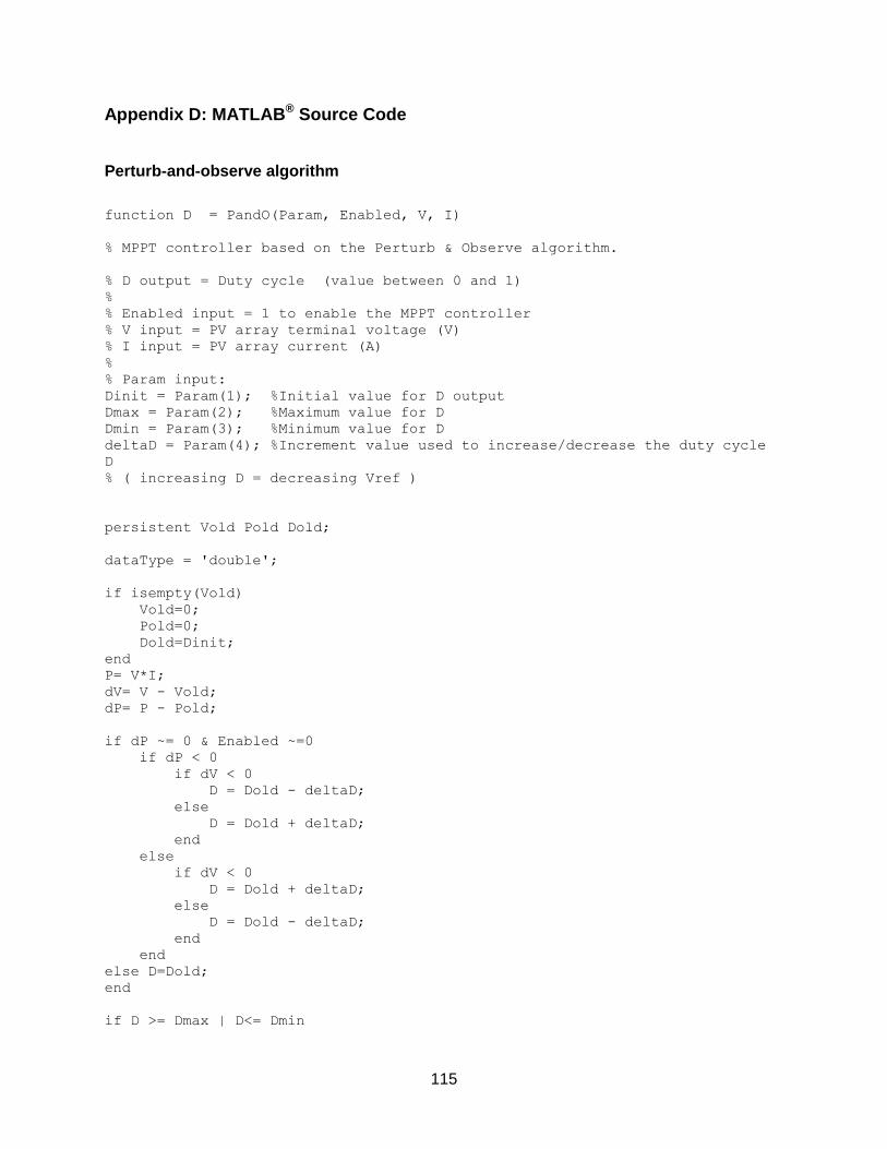
115
Appendix D: MATLAB® Source Code
Perturb-and-observe algorithm
function D = PandO(Param, Enabled, V, I)
% MPPT controller based on the Perturb & Observe algorithm.
% D output = Duty cycle (value between 0 and 1)
%
% Enabled input = 1 to enable the MPPT controller
% V input = PV array terminal voltage (V)
% I input = PV array current (A)
%
% Param input:
Dinit = Param(1); %Initial value for D output
Dmax = Param(2); %Maximum value for D
Dmin = Param(3); %Minimum value for D
deltaD = Param(4); %Increment value used to increase/decrease the duty cycle
D
% ( increasing D = decreasing Vref )
persistent Vold Pold Dold;
dataType = 'double';
if isempty(Vold)
Vold=0;
Pold=0;
Dold=Dinit;
end
P= V*I;
dV= V - Vold;
dP= P - Pold;
if dP ~= 0 & Enabled ~=0
if dP < 0
if dV < 0
D = Dold - deltaD;
else
D = Dold + deltaD;
end
else
if dV < 0
D = Dold + deltaD;
else
D = Dold - deltaD;
end
end
else D=Dold;
end
if D >= Dmax | D<= Dmin

116
D=Dold;
end
Dold=D;
Vold=V;
Pold=P;

117
Appendix E: Power Budget
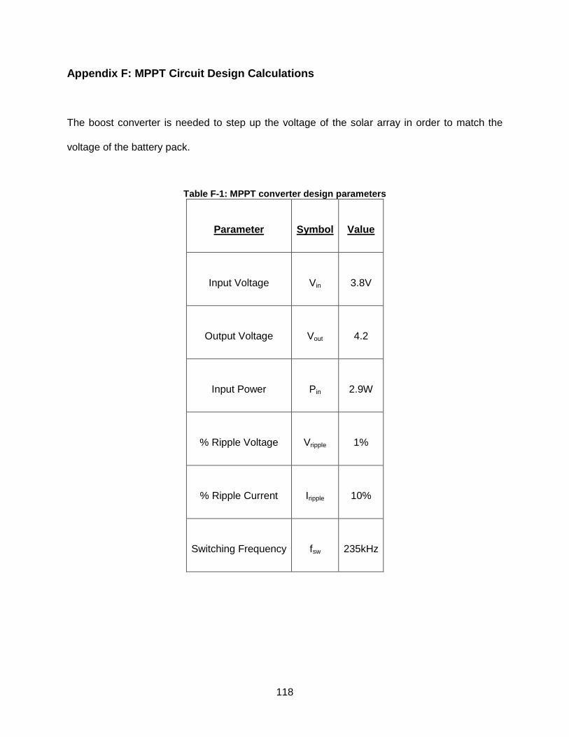
118
Appendix F: MPPT Circuit Design Calculations
The boost converter is needed to step up the voltage of the solar array in order to match the
voltage of the battery pack.
Table F-1: MPPT converter design parameters
Parameter Symbol Value
Input Voltage Vin 3.8V
Output Voltage Vout 4.2
Input Power Pin 2.9W
% Ripple Voltage Vripple 1%
% Ripple Current Iripple 10%
Switching Frequency fsw 235kHz

119
Duty cycle calculation:
out
in
V
VD 1
V
VD
2.4
88.31
076.0D
Input current:
in
inin
V
PI
V
WI in
88.3
9.2
AI in 747.0
Output current:
out
inout
V
PI
V
WIout
2.4
9.2
mAIout 47.609
Output ripple current:
100
1747.0LI
AIL 00747.0
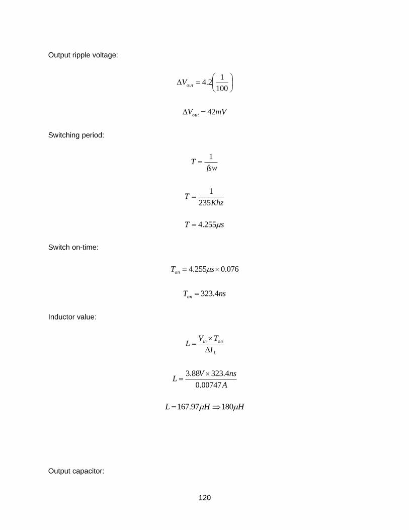
120
Output ripple voltage:
100
12.4outV
mVVout 42
Switching period:
fswT
1
KhzT
235
1
sT 255.4
Switch on-time:
076.0255.4 sTon
nsTon 4.323
Inductor value:
L
onin
I
TVL
A
nsVL
00747.0
4.32388.3
HHL 18097.167
Output capacitor:

121
swout
out
fV
DIC
KHzmV
mAC
23542
076.047.609
FFC 92.46692.4
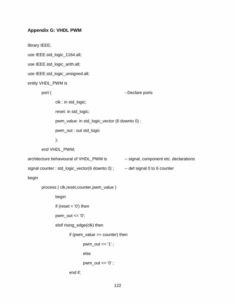
122
Appendix G: VHDL PWM
library IEEE;
use IEEE.std_logic_1164.all;
use IEEE.std_logic_arith.all;
use IEEE.std_logic_unsigned.all;
entity VHDL_PWM is
port ( --Declare ports
clk : in std_logic;
reset: in std_logic;
pwm_value: in std_logic_vector (6 downto 0) ;
pwm_out : out std_logic
);
end VHDL_PWM;
architecture behavioural of VHDL_PWM is -- signal, component etc. declarations
signal counter : std_logic_vector(6 downto 0) ; -- def signal 0 to 6 counter
begin
process ( clk,reset,counter,pwm_value )
begin
if (reset = '0') then
pwm_out <= '0';
elsif rising_edge(clk) then
if (pwm_value >= counter) then
pwm_out <= '1' ;
else
pwm_out <= '0' ;
end if;

123
end if;
end process;
process ( clk,reset )
begin
if (reset = '0') then
counter <= "0111111";
elsif rising_edge(clk) then
counter <= counter + 1;
end if;
end process;
-- architecture body
end behavioural;
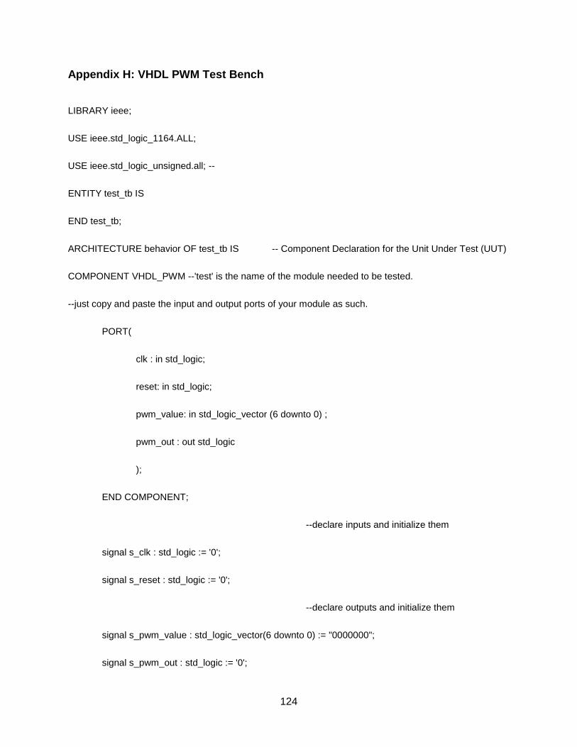
124
Appendix H: VHDL PWM Test Bench
LIBRARY ieee;
USE ieee.std_logic_1164.ALL;
USE ieee.std_logic_unsigned.all; --
ENTITY test_tb IS
END test_tb;
ARCHITECTURE behavior OF test_tb IS -- Component Declaration for the Unit Under Test (UUT)
COMPONENT VHDL_PWM --'test' is the name of the module needed to be tested.
--just copy and paste the input and output ports of your module as such.
PORT(
clk : in std_logic;
reset: in std_logic;
pwm_value: in std_logic_vector (6 downto 0) ;
pwm_out : out std_logic
);
END COMPONENT;
--declare inputs and initialize them
signal s_clk : std_logic := '0';
signal s_reset : std_logic := '0';
--declare outputs and initialize them
signal s_pwm_value : std_logic_vector(6 downto 0) := "0000000";
signal s_pwm_out : std_logic := '0';

125
-- Clock period definitions
constant clk_period : time := 125 ns;
BEGIN -- Instantiate the Unit Under Test (UUT)
uut: VHDL_PWM PORT MAP (
clk => s_clk,
pwm_value => s_pwm_value,
reset => s_reset,
pwm_out => s_pwm_out
);
-- Clock process definitions( clock with 50% duty cycle is generated here.
clk_process :process
begin
s_clk <= '0';
wait for clk_period/2; --for 0.5 ns signal is '0'.
s_clk <= '1';
wait for clk_period/2; --for next 0.5 ns signal is '1'.
end process;
-- Reset process.
reset_process :process
begin
s_reset <= '0';
wait for clk_period*10; --for 10 clocks.
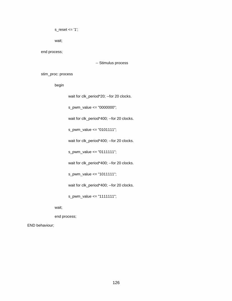
126
s_reset <= '1';
wait;
end process;
-- Stimulus process
stim_proc: process
begin
wait for clk_period*20; --for 20 clocks.
s_pwm_value <= "0000000";
wait for clk_period*400; --for 20 clocks.
s_pwm_value <= "0101111";
wait for clk_period*400; --for 20 clocks.
s_pwm_value <= "0111111";
wait for clk_period*400; --for 20 clocks.
s_pwm_value <= "1011111";
wait for clk_period*400; --for 20 clocks.
s_pwm_value <= "1111111";
wait;
end process;
END behaviour;

127
Appendix I: MATLAB® Binary Duty Cycle Calculations
%This Program calculates the Binary Value of Duty_Cycles expressed as 7 bit Binary values. It produces
2 tables: %1- rounded decimal value of the Duty cycle as well as calculated value. 2- Binary Value
clear all;
n = 0;
while (n < 100)
n=n +1 ;
value(n,1) = (n/100)*127;
value(n,2) = round((n / 100)* 127);
bin_valn,1=dec2bin(round((n / 100)* 127),7);
end

128
Appendix J: Distribution System Circuit Design Calculations
Table J-1: 5V boost converter parameters
Parameter Symbol Value
Input Voltage Vin 4.2V
Output Voltage Vout 5V
Output Power Pout 2.4W
% Ripple Voltage ∆Vo 10%
Switching Frequency fsw 235kHz
Duty cycle:
out
in
V
VD 1
5
2.41D
16.0D
Inductor value:
swf
RDDL
2
12
min
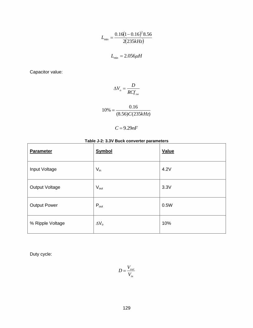
129
kHz
L2352
56.816.0116.02
min
HL 056.2min
Capacitor value:
sw
oRCf
DV
)235()56.8(
16.0%10
kHzC
nFC 29.9
Table J-2: 3.3V Buck converter parameters
Parameter Symbol Value
Input Voltage Vin 4.2V
Output Voltage Vout 3.3V
Output Power Pout 0.5W
% Ripple Voltage ∆Vo 10%
Duty cycle:
in
out
V
VD

130
2.4
3.3 VD
785.0D
Inductor value:
swf
RDL
2
1min
kHz
L2352
4.23785.01min
HL 66.10min
Capacitor value:
28
1
sw
oLCf
DV
2)235()66.10(8
785.0101.0
kHzCH
HHC 65.45565.4

131
Appendix K: System Integration

132