au/ag bilayered metal mesh as a si etching catalyst for ... nano5_3229_2011.pdf · au/ag bilayered...
TRANSCRIPT

KIM ET AL. VOL. 5 ’ NO. 4 ’ 3222–3229 ’ 2011
www.acsnano.org
3222
March 09, 2011
C 2011 American Chemical Society
Au/Ag Bilayered Metal Mesh as a SiEtching Catalyst for ControlledFabrication of Si NanowiresJungkil Kim,†,§ Hee Han,† Young Heon Kim,† Suk-Ho Choi,§ Jae-Cheon Kim,† and Woo Lee†,‡,*
†Korea Research Institute of Standards and Science (KRISS), Yuseong, 305-340 Daejeon, Korea, ‡University of Science and Technology (UST), Yuseong, 305-333Daejeon, Korea, and §Department of Applied Physics, Kyung Hee University, Yongin 446-701, Korea
Silicon nanowires (SiNWs) have at-tracted much attention because oftheir many unique properties and po-
tential applications as building blocks foradvanced electronic devices, biological sen-sors, and optoelectronic devices, as well asfor renewable energy devices.1-6 For bothfundamental studies and practical applica-tions of SiNWs, fabrication of ordered arraysof SiNWs with precise control of the loca-tion, diameter, length, and density will be ofgreat value. Moreover, it is of utmost im-portance to synthesize SiNWs with con-trolled crystal orientations and morpholo-gies because of the close relation betweenphysicochemical properties of SiNWs andtheir detailed crystal structures, as in manynanostructured low-dimensional materials.Among many fabrication methods, metal-assisted chemical etching (MaCE) has re-cently attracted considerable attention asa promising alternative SiNW fabrication. Inthis approach, noble metals (e.g., Ag, Au, Pt,etc.) on a silicon substrate are used ascatalysts in the chemical etching of siliconwith an aqueous solution containing HF andanoxidant (H2O2ormetal salts, suchasAgNO3,KAuCl4, K2PtCl6, Fe(NO3)3, Mn(NO3)3).
2-4,6-16
It is generally accepted that a metal actsas a microscopic cathode withdrawingelectrons from the underlying silicon (i.e.,injection of positive holes (hþ) into silicon)through metal-silicon quasi-Schottky inter-face, and also as a catalyst for the decom-position or reduction of the oxidants.11,12
As a result of the microscopic electrochemi-cal process, the silicon that comes in directcontact with a metal undergoes oxidativedissolution in a solution containing HF,maintaining a metal-silicon junction andthus enabling continued movement of theetching front (i.e., metal/silicon interface).Several SiNW fabrication methods employ-ing MaCE have been reported. One of the
most intensively utilized methods is wetchemical etching of silicon substrates witha catalyst consisting of interconnected net-works of metal nanoparticles (NPs) thatcan be deposited either by galvanic displa-cement from a mixture solution containingHF and metal salt or by sputter deposi-tion.2,3,6-17 However, the resulting SiNWsexhibit poor spatial ordering and broaddiameter distribution due to the randomtwo-dimensional (2D) networks of nonuni-form metal nanoparticles (see SupportingInformation, Figure S1). On the other hand,recent developments have shown that MaCEutilizing metal thin film patterned on asilicon substrate offers several distinct ad-vantages over nanoparticle-based MaCE interms of control of the location, diameter,spacing, and density of aligned SiNWs.18-23
Patterning of metal thin films with arrays ofnanoholes have been achieved by utilizingpolystyrene beads, block copolymers, orultrathin anodic aluminum oxide (AAO) aspatterning masks or by employing laserinterference lithography or focused ionbeam (FIB) technique.18-24 However, thereported patterning methods involve com-plicated processing steps, requiring multi-ple processes (e.g., sputter deposition of SiO2,resist removal, oxygen plasma treatment, and
* Address correspondence [email protected].
Received for review January 27, 2011and accepted March 9, 2011.
Published online10.1021/nn2003458
ABSTRACT Au/Ag bilayered metal mesh with arrays of nanoholes were devised as a catalyst for
metal-assisted chemical etching of silicon. The present metal catalyst allows us not only to overcome
drawbacks involved in conventional Ag-based etching processes, but also to fabricate extended
arrays of silicon nanowires (SiNWs) with controlled dimension and density. We demonstrate that
SiNWs with different morphologies and axial orientations can be prepared from silicon wafers of a
given orientation by controlling the etching conditions. We explored a phenomenological model that
explains the evolution of the morphology and axial crystal orientation of SiNWs within the
framework of the reaction kinetics.
KEYWORDS: silicon nanowires . metal-assisted chemical etching .Au/Ag bilayered metal mesh . anodic aluminum oxide (AAO) . anodization
ARTIC
LE

KIM ET AL. VOL. 5 ’ NO. 4 ’ 3222–3229 ’ 2011
www.acsnano.org
3223
reactive ion etching (RIE)) as well as special techniquesfor mask preparation. The surfaces of the fabricatedSiNWs are often contaminated with numerous metalnanoparticles, which cause porosification of SiNWs dueto undesired chemical etching of the wire surface.19,20
Herein, we report a straightforward and readily acces-sible method for synthesizing extended arrays ofSiNWs with controlled dimensions. Our approach isbased on MaCE of silicon wafers by using Au/Agbilayered metal meshes with arrays of nanoholes thatcan conveniently be prepared from AAO membranes,overcoming some of the drawbacks involved in con-ventional MaCE processes using randomly distributedAg nanoparticles or patterned Ag films. We furthershow that arrays of SiNWs with different axial orienta-tions andmorphologies can be prepared from a siliconwafer of a given orientation by changing the etchingparameters. We provide a phenomenological modelthat explains the evolution of the morphology andaxial crystal orientation of SiNWs within the frameworkof the reaction kinetics.
RESULTS AND DISCUSSION
Au/Ag Bilayered Metal Meshes for Controlled Fabrication ofSiNWs. Previously, silver has been popularly employedas a catalyst material for the synthesis of SiNWs arraysby MaCE of silicon because of its superior etchingperformance over other metal catalysts (e.g., Au, Pt,Cu, or Fe). However, our studies revealed that a silvermesh with regular arrays of nanoholes undergoesdissolution-induced structural failure during siliconetching for an extended period of time or at anelevated etching temperature, which prevents
preparation of uniformly aligned SiNWs with con-trolled diameter and density (see Supporting Informa-tion, Figure S2). The problem associated withdissolution of silver metal catalyst becomes serious asthe thickness of the patterned silver film decreases.This observation is somewhat in line with the recentreports that silver can be anodically dissolved in anetchant solution containing HF and H2O2 (Agþ/Ago,1.72 V vs NHE at pH 0.3), giving rise to surface rough-ening or porosification of the resulting SiNWs.6,13,25 Infact, Huang et al. reported recently that short SiNWs(aspect ratio = ca. 5) prepared by using a patterned thinfilm of silver have tapered morphologies with differentdiameters at the top and the bottompart duemainly tothe dissolution-induced gradual increase of the holesizes of silver film during etching even for a shortperiod of time (10-30 s).19,20 To overcome theseproblems, we devised a new type of metal mesh witha Au/Ag-stacking configuration, in which the Ag sidecomes in contact with the polished surface of a siliconwafer during MaCE reaction. Since Au is inert againstoxidative dissolution in a mixture solution of HF andH2O2, the upper Au layer in our Au/Ag bilayered metalmesh can effectively prevent not only undesired struc-tural disintegration of the underlying Ag layer but alsotapering of SiNWs (vide infra), still acting as a catalystfor H2O2 decomposition on its surface (i.e., H2O2þ 2Hþ
þ 2e- f 2H2O).The experimental procedure employed in the pre-
sent work is schematically illustrated in Figure 1.Fifteen nm-thick Ag and 5 nm-thick Au were sequen-tially sputtered onto an AAO membrane at a deposi-tion rate of 10 nm/min (Figure 1a). The Au/Ag-coated
Figure 1. Schematic of the SiNW fabrication process: (a) sequential sputter depositions of Ag and Au on the surface of AAOmembrane; (b) transfer of Au/Ag bilayeredmetal mesh onto a siliconwafer from the surface of etching solution after removalof AAO membrane and also loosely bound metal nanoparticles from the bottom side of the metal mesh; (c) metal-assistedchemical etching (MaCE) of (100)-oriented silicon wafer for the fabrications of SiNWs with controlled axial orientations andmorphologies; (d) a photograph of Au/Ag bilayered metal mesh on a Si(100) wafer.
ARTIC
LE

KIM ET AL. VOL. 5 ’ NO. 4 ’ 3222–3229 ’ 2011
www.acsnano.org
3224
AAO membrane was floated on the surface of anetching solution (0.1 M NaOH, room temp) to releaseAu/Ag bilayered metal mesh from the oxide mem-brane. The resulting metal mesh remained floating onthe surface of the aqueous etching solution and couldbe easily transferred onto any substrates. The edges ofnanoholes at the bottom side of the metal mesh werecontaminated with loosely connected metal nanopar-ticles, which were originated from themetal depositedinto the pore walls of oxide nanopores during thesputter deposition process. It should be noted thatnanometer-sized metal particles participate in theetching reaction during MaCE of a silicon substrate,resulting in SiNWs with irregular surface etch profiles.Therefore, it is recommended to remove the undesiredmetal nanoparticles from the bottom side of a metal,which can be achieved by floating the sample forabout 5 s on a diluted nitric acid solution (10 wt %HNO3). After removal of metal nanoparticles, nitric acidsolution was replaced with deionizedwater, and finallywith a silicon etching solution. The resulting metalmesh was transferred onto a silicon substrate (Figure 1b).Subsequently, the sample was dried to remove theresidual amount of silicon etching solution from theinterface between the metal mesh and the underlyingsilicon substrate. The silicon surface contacting withmetal was partially etched during the drying step.Since a conformal contact between the metal meshand the underlying silicon surface was establishedupon drying, the metal mesh was not separated fromthe silicon surface even if the sample was exposed to astrong stream of water or nitrogen jet. Fabrication ofarrays of SiNWs with controlled morphology and axial
orientation could be achieved by immersing metalmesh-loaded silicon wafers (B-doped, resistivity =1-10 Ωcm) into mixture solutions of HF (46 wt %),H2O2 (35 wt %), and H2O at temperatures ranging from20 to 70 �C in ambient light (Figure 1c). Ourprocess allowed us to obtain a wrinkle-free metalmesh (diameter = ca. 4 cm) on a silicon wafer(Figure 1d), and thus to prepare uniform arrays ofepitaxial SiNWs on the entire silicon surface coveredwith metal mesh.
AAO membranes have been utilized as versatile tem-plate materials for fabricating 2D extended arrays ofvarious functional nanostructures due to the uniquetailoring capability of the pore size, pore density, poreshape (e.g., circular, square, or triangular pore openings),as well as 2D arrangement of oxide nanopores.26-29 AAOmembranes with a uniform pore diameter in the rage of20-400 nm and with a pore density in the range of108-1010/cm2 can conveniently be prepared by anodicoxidation of aluminum.27 Moreover, oxide nanopores ofan as-prepared AAO membrane can be enlarged in atightly controlled manner via a pore wall etching processby using an H3PO4 solution.30 Figure 2 panels a and bdisplay representative scanning electron microscopy(SEM) images of AAO membrane and Au/Ag bilayeredmetal mesh prepared from it, respectively. The structureof metal mesh is characterized by an ultrathin filmperforated by arrays of nanoholes, in which hole arraypattern, hole shape, and pitch distance are identical tothose of the AAO replication master. It was observed thatan averagenanohole size of an as-preparedmetalmesh isslightly smaller than that of the pore openings of the AAOmembrane used for mesh replication. This can be
Figure 2. SEM micrographs of (a) AAO membrane and (b) Au/Ag bilayered metal mesh. (c) Typical plan-view SEM image ofextended arrays of vertically aligned SiNWs obtained by metal-assisted chemical etching (MaCE) of Si(100) wafers by usingAu/Ag bilayered metal mesh. (d,e) Cross-sectional SEM images of vertically etched Si(100) wafers, showing SiNWs withdifferent diameters; (d) 63.9 ( 9.2 and (e) 39.5 ( 4.2 nm. (f) A magnified cross-sectional SEM image of a vertically etchedSi(100) wafer taken near the etching front. (g) Histogram showing the diameter distribution of SiNWs shown in panel c,together with a Gaussian fit (solid line) of the measured statistical data.
ARTIC
LE
KIM ET AL. VOL. 5 ’ NO. 4 ’ 3222–3229 ’ 2011
www.acsnano.org
3225
attributed to the progressive decrease of the hole size ofmetal mesh as a function of deposition time during themetal sputtering process (i.e., the closure effect).31
Figure 2c-f show typical SEM micrographs of extendedarrays of vertically aligned SiNWs fabricated by MaCE of(100)-oriented silicon wafers at room temperature byusing Au/Ag bilayered metallic meshes where panel c isthe top-view and panels d-f are the cross-section views.Our microscopic investigation indicated that spatial ar-rangements of nanowires follow exactly the hole arraypattern of metal mesh (Figure 2c). To get access to thequantitative information on the size distribution of SiNWs,we performed real-space image analysis on the SEMmicrograph shown in Figure 2cbyusing a standard imageprocessing package (e.g., ImageJ).32 According to statis-tical analysis, the mean and standard deviation of thenanowire diameters turned out to be 49.1 ( 5.1 nm(Figure 2g). In the present study, we were able to achievefine control of the diameter of SiNWs without affectingtheir separations (ca. 100 nm) by taking advantage of thegeneric tailoring capability of the pore size of the AAOmembrane through the pore wall etching process, asdemonstrated in Figure 2d (diameter = 63.9 ( 9.2 nm)and Figure 2e (diameter = 39.5 ( 4.2 nm). It should bementioned that our nanowire samples exhibit fairly uni-form etching fronts (i.e., the interface between metalmesh and the underlying silicon substrate), revealinghomogeneous metal-assisted etching of silicon withoutstructural failure of catalyst metal mesh (Figure 2d-f).Moreover, individual nanowires have smooth surfaces
and uniform diameters along their axes withoutshowing tapered morphology, which can be ascribed tothe inert nature of the Au layer of our bilayeredmetal mesh against anodic dissolution as discussedearlier.
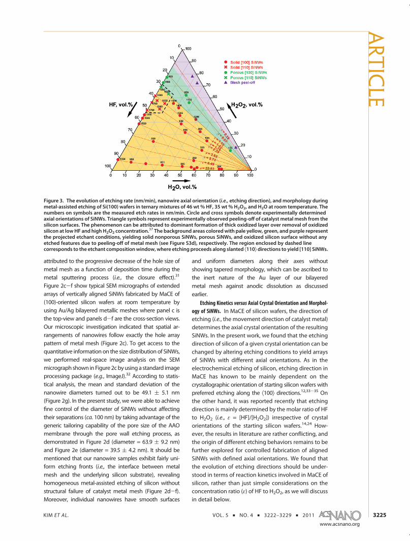
Etching Kinetics versus Axial Crystal Orientation and Morphol-ogy of SiNWs. In MaCE of silicon wafers, the direction ofetching (i.e., the movement direction of catalyst metal)determines the axial crystal orientation of the resultingSiNWs. In the present work, we found that the etchingdirection of silicon of a given crystal orientation can bechanged by altering etching conditions to yield arraysof SiNWs with different axial orientations. As in theelectrochemical etching of silicon, etching direction inMaCE has known to be mainly dependent on thecrystallographic orientation of starting silicon wafers withpreferred etching along the Æ100æ directions.12,33-35 Onthe other hand, it was reported recently that etchingdirection is mainly determined by the molar ratio of HFto H2O2 (i.e., ε = [HF]/[H2O2]) irrespective of crystalorientations of the starting silicon wafers.14,24 How-ever, the results in literature are rather conflicting, andthe origin of different etching behaviors remains to befurther explored for controlled fabrication of alignedSiNWs with defined axial orientations. We found thatthe evolution of etching directions should be under-stood in terms of reaction kinetics involved in MaCE ofsilicon, rather than just simple considerations on theconcentration ratio (ε) of HF to H2O2, as we will discussin detail below.
Figure 3. The evolution of etching rate (nm/min), nanowire axial orientation (i.e., etching direction), andmorphology duringmetal-assisted etching of Si(100) wafers in ternary mixtures of 46 wt % HF, 35 wt % H2O2, and H2O at room temperature. Thenumbers on symbols are the measured etch rates in nm/min. Circle and cross symbols denote experimentally determinedaxial orientations of SiNWs. Triangle symbols represent experimentally observed peeling-off of catalyst metal mesh from thesilicon surfaces. The phenomenon can be attributed to dominant formation of thick oxidized layer over removal of oxidizedsilicon at lowHF and high H2O2 concentration.
37 The background areas coloredwith pale yellow, green, and purple representthe projected etchant conditions, yielding solid nonporous SiNWs, porous SiNWs, and oxidized silicon surface without anyetched features due to peeling-off of metal mesh (see Figure S3d), respectively. The region enclosed by dashed linecorresponds to the etchant compositionwindow,where etching proceeds along slanted Æ110æ directions to yield [110] SiNWs.
ARTIC
LE

KIM ET AL. VOL. 5 ’ NO. 4 ’ 3222–3229 ’ 2011
www.acsnano.org
3226
Figure 3 shows the evolution of etching rate(in nm/min), etching direction (i.e., nanowire axialorientation), and morphology (solid nonporous vs
porous) of SiNWs during MaCE of Si(100) wafers internary mixtures of HF, H2O2, and H2O at room tem-perature. Each red line in the present ternary diagramrepresents the solution composition of the samemolarratio (ε) of HF to H2O2. Experimentally observed verticaletchings and slanted ones are marked with circle andcross symbols, respectively. The numbers on symbolsare the measured etch rates in nm/min. The verticaletchings are defined as the movement of the etchingfront perpendicular to the wafer surface, resulting in[100] SiNWs. On the other hand, the slanted etchingsare defined as those proceeding in inclined directions(tilted by 45�) with respect to the surface normal,resulting in [110] SiNWs. Under our experimental con-ditions, we could not observe etching along the Æ111ædirections that are tilted by 35.3� from the wafer sur-face (i.e., (100) plane). Representative electron micro-graphs of SiNWs obtained from a vertical Æ100æ etchingand a slanted Æ110æ one are shown in Figure 4. Contraryto the recent reports,14,24 one may see from Figure 3that there is no correlation between the etching
direction and the concentration ratio (ε) of HF toH2O2, although the latter appears to affect the mor-phology of the resulting SiNWs (i.e., solid nonporousSiNWs at ε g 1.15 and porous SiNWs at 0.3 < ε e 1.15;see Figure S3 for morphologies of silicon nanostruc-tures formed at ε < 1.15). It turned out that etchingsalong slanted Æ110æ directions occur within a narrowwindow of solution composition, giving highetching rates (the region enclosed by dashed line inFigure 3). It appears that etching direction is mainlydictated by the etching rate, that is, etching occursalong vertical Æ100æ directions at low etching rates,while occurring along slanted Æ110æ directions at highetching rates.
In MaCE of silicon, the movement of the etchingfront (i.e., metal/silicon interface) is a net consequenceof the following two competing events; injection of apositive hole (hþ) into bulk silicon through the metal-silicon quasi-Schottky interface (a process accompany-ing partial oxidation of silicon) and removal of oxidizedsilicon by HF from just underneath the catalyst metal.Therefore, the overall etching rate would be governedby the interplay between these two processes. Sincethe generation of holes (hþ) is related to the catalyticdecomposition of H2O2 at the interface between thebulk electrolyte and the catalyst metal surface, theamount of holes (hþ) injected into silicon is propor-tional to the H2O2 concentration or its decompositionactivity which increases with temperature (vide infra).On the other hand, removal of oxidized silicon by HF isassociated with the cleavage of its back bonds,36 ofwhich effective number density in different crystalplanes increases with the order {100} < {110} <
Figure 4. Representative cross-sectional SEM micrographsof SiNWs formed by (a) vertical and (b) slanted etching ofSi(100) wafers. (c,d) High-resolution transmission micro-scopy (HRTEM) images of SiNWs taken from the samplesshown in panels a and b, respectively. The correspondingfast Fourier transform (FFT) patterns of HRTEM images inpanels c and d are displayed below the respective panels,from which the directions of etching were confirmed to beÆ100æ and Æ110æ for the samples shown in panels a and b,respectively. Note that, in a Si(100) wafer, fracture occurspreferentially along Æ110æ directions.41 Accordingly, viewedfrom [110] axis, SiNWs formedby [101] etching appear to betiled by 54.7� with respect to the wafer surface (althoughthey are actually tiled by 45�), as denoted by the dashedarrow in panel b.
Figure 5. Arrhenius plots showing the temperature de-pendence of the etching rates (ln(rate) vs 1/T) for metal-assisted etching of (100)-oriented silicon wafers by usingetchant solutions with different compositions, in which theconcentration of H2O2 was varied in the range 0.242-1.057Mby controlling the amount of water, while themolar ratio ofHF to H2O2 was fixed to ε = 22.931. Blue symbols representexperimentallymeasured rates of etching along the verticalÆ100æ direction, while red ones represent rates of etchingalong the slanted Æ110æ directions. The solid lines representthe best fits to the experimental data.
ARTIC
LE

KIM ET AL. VOL. 5 ’ NO. 4 ’ 3222–3229 ’ 2011
www.acsnano.org
3227
{111} (see Supporting Information, Table S1). Undersolution conditions ensuring ready removal of oxidizedsilicon (i.e., etching solutions with high [HF]), catalyticdecomposition of H2O2 would become the rate deter-mining process. In other words, the etching rate isproportional to the amount of positive holes (hþ)injected into silicon (i.e., reaction rate � [H2O2]), andthe following etching behaviors will operate: At lowH2O2 concentration, hole (hþ) injection into siliconatoms will be localized at the (100) plane, where thereare the fewest silicon back bonds to break, resulting inetching along the Æ100æ direction. As the concentrationof H2O2 increases sufficiently and thereby the amountof the generated holes (hþ) exceeds a certain thresh-old, removal of silicon atoms would occur with greatrapidity in the crystal planes, where there are moresilicon back bonds to polarize, resulting in Æ110æ andeven possibly Æ111æ etchings. Analogously, the follow-ing etching behaviors will operate for the solutionconditions ensuring a large generation of positiveholes (hþ) (i.e., etching solutions with high [H2O2]), inwhich removal of oxidized silicon byHF governs overalletching reaction (i.e., reaction rate � [HF]) and alsoetching direction: At low HF concentration, removal ofoxidized silicon will take place slowly in the leastcompact (100) plane due to limited amount of HF. Inthe mean time, an extra amount of injected holes (hþ)can readily diffuse away from the etching front tolattice defects and dopant sites (pore nucleation sites)on the surface of the already formed SiNWs,3,11,37-39
resulting in porous [100] SiNWs. At high HF concentra-tion, on the other hand, removal of oxidized siliconwould be kinetically favored in the crystal planes with ahigher density of silicon back bonds, resulting in etch-ings along non-Æ100æ directions. Porous nanowiremorphology may emerge, if there are extra holes (hþ)that are not consumed completely at the etching front.In other words, both high H2O2 concentration for largegeneration of positive holes (hþ) and low HF concen-tration for limited removal of oxidized silicon arethe necessary condition for porous nanowireformation (i.e., etching solutions with low [HF]/[H2O2]ratio, ε).
Etching Directions versus Activation Energies. The presentkinetic relevance of the etching directions could becorroborated by demonstrating that MaCE of Si(100)wafers with etching solutions of a fixed [HF]/[H2O2]ratio (ε = 22.931) can result in switching of theetching direction from vertical Æ100æ at room tem-perature to slanted Æ110æ at elevated temperature.Since decomposition activity of H2O2 on the surfaceof catalyst metal increases with temperature,40 hole(hþ) injection into silicon can be promoted at anelevated temperature. Correspondingly, tempera-ture positively correlates with the etching rate, pro-vided that HF is readily available (i.e., high [HF]).Figure 5 shows the temperature dependence of the
etching rates (i.e., Arrhenius plots; ln(R) = ln(A) -Ea/(kBT), where R is the etching rate, A is the pre-exponential (frequency) factor, Ea is the activationenergy for etching, and kB is the Boltzmann constant-). Etched in solutions with [H2O2] e 0.485 M, etchingproceeded always along the vertical Æ100æ directioneven though the temperature was varied from 20 to70 �C. In contrast, for etchant solutions with [H2O2]g0.727 M, switching of the etching direction fromvertical Æ100æ to slanted Æ110æ took place at anelevated temperature. Upon closer examination ofthe present kinetic plots, one may see that theswitching temperature decreases with increase inH2O2 concentration, and switching of the etchingdirection is accompanied by changes of the slopes.According to our analysis, averaged activation en-ergy for Æ110æ etching turned out to be higher thanthat for Æ100æ etching; EaÆ110æ = 0.57 ( 0.03 eV andEa
Æ100æ = 0.35 ( 0.05 eV. The activation energy foretching corresponds to the energy barrier for displa-cing a silicon atom from its site. We attribute theobserved higher activation energy for Æ110æ etchingto higher density of silicon back bonds in (110) planecompared to the (100) one. On the other hand, theobserved H2O2 concentration dependence of theswitching temperature strongly implies that thereis a threshold amount of the positive holes (hþ).Above the threshold, weakening of silicon backbonds in the (110) planemay occur effectively. Belowthe threshold, however, hole injection will be limitedto the silicon atoms in the (100) plane resulting inetching along the Æ100æ direction, even if the etchingrate is high enough due to increased reaction tem-perature. We propose here that etching along thenon-Æ100æ directions occurs only if the etching con-dition can guarantee both the generation of a largeamount of positive holes (hþ) and the fast removal ofoxidized silicon by HF (i.e., a condition satisfying fastetching reaction). Although we mainly discussedthe evolution of the morphology and axial orienta-tion of SiNWs during MaCE of Si(100) wafers, ourpreliminary results indicate that the argumentsmade above can be generally applied to non-(100)-oriented Si wafers.
CONCLUSION
We developed Au/Ag bilayered metal meshes withregular hexagonal arrays of nanoholes as a catalyst forwet-chemical etching of silicon. The newly developedetching catalyst allows us not only to overcome draw-backs involved in conventional Ag-based silicon etch-ing processes, but also to fabricate arrays of uniformsilicon nanowires. We demonstrated that SiNWs withdifferent axial orientations and morphologies can beprepared from a silicon wafer of a given orientation bydeliberately controlling the etching conditions. Our
ARTIC
LE

KIM ET AL. VOL. 5 ’ NO. 4 ’ 3222–3229 ’ 2011
www.acsnano.org
3228
results revealed that reaction kinetics has profoundimplication for the evolution of morphology and axial
orientation of SiNWs during metal-assisted chemicaletching of silicon.
METHODSMembrane Preparation. Free-standing self-ordered nanopor-
ous anodic aluminum oxide (AAO) membrane was prepared byanodization of aluminum as follow: As-received aluminum discs(Goodfellow, 99.999%) were used in anodization experimentswithout the annealing step. On the other hand, the aluminumdiscs were electrochemically polished in an 1:4 mixture solutionof 65% HClO4 and 99.5% ethanol (5 �C) in order to exclude, ifany, potential side effects (e.g., localized field concentration)that could arise from the surface roughness during anodization.A surface finished aluminum disk was placed in an electroche-mical cell with an O-ring, so that one side of metal could beanodized. Anodization was conducted under a regulated cellvoltage of 40 V using 0.3 M H2C2O4 (5 �C) as an electrolyte for15 h. Anodization of aluminum in the presentworkwas performedby using an electrochemical cell equipped with a cooling stagethat is in thermal contact with the aluminum substrate toremove the reaction heat.26 After anodization, the remainingAl substratewas selectively removedby using amixture solutioncontaining 3.4 g CuCl2 3 2H2O, 50 mL of 38 wt % HCl, and 100 mLof DI water. The bottom surface of AAO that originally came incontact with the aluminum substrate is sealed by a ca. 46 nm-thick barrier oxide layer. This barrier oxide layer was removed byexposing the bottom surface of AAO to 5 wt % H3PO4 (30 �C) for30 min to obtain a through-channel membrane.
Pretreatment of Si Wafers. A set amount of (100)-oriented p-Siwafers (B-doped, F = 1-10Ωcm) were cleaned by using either aRCA solution (NH3 3H2O/H2O2/H2O, v/v/v = 1/1/5) or a Piranhasolution (98% H2SO4/30% H2O2, v/v = 4/1) and then thoroughlyrinsed by copious amounts of deionized (DI) water prior to use.
Microscopic Characterization. A Hitachi S-4800 field emissionscanning electron microscope (FE-SEM) was employed for themorphological characterization of the samples. The sampleswere mechanically cleaved for the cross-sectional SEM investi-gations. The crystallographic orientation of the SiNWs wereinvestigated by a transmission electron microscope (TEM, Tec-nai F30, FEI, USA) operated at a primary beam energy of 300 kV.To prepare specimens for TEM investigation, the surface of anetched Si substrate was scraped using a razor blade, and SiNWsin the scrapings were collected and dispersed in absoluteethanol. A drop of the resulting suspension solution was placedon a carbon-coated Cu grid.
Acknowledgment. This research was supported by Future-based Technology Development Program (Nano Fields)through the National Research Foundation of Korea (NRF)funded by the Ministry of Education, Science and Technology(Grant No. 2010-0029332), and in part by Korea ResearchCouncil of Fundamental Science and Technology (KRCF)through the KRISS project of “Development of Advanced In-dustrial Metrology”.
Supporting Information Available: SEM micrographs ofSiNWs fabricated with randomly distributed silver nanoparticlesand silver mesh with arrays of nanoholes; SEM micrographs ofsilicon nanostructures formed at ε < 1.15; table showing therelationship among surface bond orientation, atomic arrange-ment, and silicon back-bond density for Si(100), Si(110), andSi(111) planes. This material is available free of charge via theInternet at http://pubs.acs.org.
REFERENCES AND NOTES1. Chan, C. K.; Peng, H.; Liu, G.; McIlwrath, K.; Zhang, X. F.;
Huggins, R. A.; Cui, Y. High-Performance Lithium BatteryAnodes Using Silicon Nanowires. Nat. Nanotechnol. 2008,3, 31–35.
2. Hochbaum, A. I.; Chen, R.; Delgado, R. D.; Liang,W.; Carnett,E. C.; Najarian, M.; Majumdar, A.; Yang, P. EnhancedThermoelectric Performance of Rough Silicon Nanowires.Nature 2008, 451, 163–167.
3. Hochbaum, A. I.; Gargas, D.; Hwang, Y. J.; Yang, P. SingleCrystalline Mesoporous Silicon Nanowires. Nano Lett.2009, 9, 3550–3554.
4. Kelzenberg, M. D.; Boettcher, S. W.; Petykiewicz, J. A.;Turner-Evans, D. B.; Putnam, M. C.; Warren, E. L.; Spurgeon,J. M.; Briggs, R. M.; Lewis, N. S.; Atwater, H. A. EnhancedAbsorption and Carrier Collection in Si Wire Arrays forPhotovoltaic Applications. Nat. Mater. 2010, 9, 239–244.
5. Park, M.-H.; Kim, M. G.; Joo, J.; Kim, K.; Kim, J.; Ahn, S.; Cui, Y.;Cho, J. Silicon Nanotube Battery Anodes. Nano Lett. 2009,9, 3844–3847.
6. Qu, Y.; Liao, L.; Li, Y.; Zhang, H.; Huang, Y. ElectricallyConductive andOptically Active Porous SiliconNanowires.Nano Lett. 2009, 9, 4539–4543.
7. Peng, K.; Wu, Y.; Fang, H.; Zhong, X.; Xu, Y.; Zhu, J. Uniform,Axial-Orientation Alignment of One-Dimensional Single-Crystal Silicon Nanostructure Arrays. Angew. Chem., Int. Ed.2005, 44, 2737–2742.
8. Peng, K.; Fang, H.; Hu, J.; Wu, Y.; Zhu, J.; Yan, Y.; Lee, S. T.Metal-Particle-Induced, Highly Localized Site-SpecificEtching of Si and Formation of Single-Crystalline Si Nano-wires in Aqueous Fluoride Solution. Chem.;Eur. J. 2006,12, 7942–7947.
9. Peng, K.; Hu, J.; Yan, Y.; Wu, Y.; Fang, H.; Xu, Y.; Lee, S. T.; Zhu,J. Fabrication of Single-Crystalline Silicon Nanowires byScratching a Silicon Surface with Catalytic Metal Particles.Adv. Funct. Mater. 2006, 16, 387–394.
10. Fang, H.; Wu, Y.; Zhao, J.; Zhu, J. Silver Catalysis in theFabrication of Silicon Nanowire Arrays. Nanotechnology2006, 17, 3768–3774.
11. Li, X.; Bohn, P. W. Metal-Assisted Chemical Etching in HF/H2O2 Produces Porous Silicon. Appl. Phys. Lett. 2000, 77,2572–2574.
12. Peng, K.; Lu, A.; Zhang, R.; Lee, S.-T. Motility of MetalNanoparticles in Silicon and Induced Anisotropic SiliconEtching. Adv. Funct. Mater. 2008, 18, 3026–3035.
13. Zhang,M.-L.; Peng, K.-Q.; Fan, X.; Jie, J.-S.; Zhang, R.-Q.; Lee,S.-T.; Wong, N.-B. Preparation of Large-Area UniformSilicon Nanowires Arrays Through Metal-Assisted Chemi-cal Etching. J. Phys. Chem. C 2008, 112, 4444–4450.
14. Huang, Z.; Shimizu, T.; Senz, S.; Zhag, Z.; Geyer, N.; G€osele,U. Oxidation Rate Effect on the Direction ofMetal-AssistedChemical and Electrochemical Etching of Silicon. J. Phys.Chem. C 2010, 114, 10683–10690.
15. Peng, K.-Q.; Yan, Y.-J.; Gao, S.-P.; Zhu, J. Synthesis ofLarge-Area Silicon Nanowire Arrays via Self-AssemblingNanoelectrochemistry. Adv. Mater. 2000, 14, 1164–1167.
16. Peng, K.; Xu, Y.; Wu, Y.; Yan, Y.; Lee, S.-T.; Zhu, J. AlignedSingle-Crystalline Si Nanowire Arrays for PhotovoltaicApplications. Small 2005, 1, 1062–1067.
17. Chen, H.; Wang, H.; Zhang, X.-H.; Lee, C.-S.; Lee, S.-T. Wafer-Scale Synthesis of Single-Crystal Zigzag Silicon NanowireArrayswith Controlled Turning Angle.Nano Lett. 2010, 10,864–868.
18. Huang, Z.; Fang, H.; Zhu, J. Fabrication of Silicon NanowireArrays with Controlled Diameter, Length, and Density.Adv. Mater. 2007, 19, 744–748.
19. Huang, Z.; Shimizu, T.; Senz, S.; Zhang, Z.; Zhang, X.; Lee,W.; Geyer, N.; G€osele, U. Ordered Arrays of VerticallyAligned [110] Silicon Nanowires by Suppressing the Crys-tallographically Preferred Æ100æ Etching Directions. NanoLett. 2009, 9, 2519–2525.
ARTIC
LE

KIM ET AL. VOL. 5 ’ NO. 4 ’ 3222–3229 ’ 2011
www.acsnano.org
3229
20. Huang, Z.; Zhang, X.; Reiche, M.; Liu, L.; Lee, W.; Shimizu, T.;Senz, S.; G€osele, U. Extended Arrays of Vertically AlignedSub-10 nmDiameter [100] Si Nanowires byMetal-AssistedChemical Etching. Nano Lett. 2008, 8, 3046–3051.
21. Chang, S.-W.; Chuang, V. P.; Boles, S. T.; Ross, C. A.;Thompson, C. V. Densely Packed Arrays of Ultra-High-Aspect-Ratio Silicon Nanowires Fabricated Using Block-Copolymer Lithography and Metal-Assisted Etching. Adv.Funct. Mater. 2009, 19, 2495–2500.
22. Huang, J.; Chiam, S. Y.; Tan, H. H.; Wang, S.; Chim, W. K.Fabrication of Silicon Nanowires with Precise DiameterControl Using Metal Nanodot Arrays as a Hard MaskBlocking Material in Chemical Etching. Chem. Mater.2010, 22, 4111–4116.
23. de Boor, J.; Geyer, N.; Wittemann, J. V.; G€osele, U.; Schmidt,V. Sub-100 nm Silicon Nanowires by Laser InterferenceLithography and Metal-Assisted Etching. Nanotechnology2010, 21, 095302.
24. Chern, W.; Hsu, K.; Chun, I. S.; Azeredo, B. P. d.; Ahmed, N.;Kim, K.-H.; Zhu, J.-m.; Fang, N.; Ferreira, P.; Li, X. Nonlitho-graphic Patterning and Metal-Assisted Chemical Etchingfor Manufacturing of Tunable Light-Emitting SiliconNanowire Arrays. Nano Lett. 2010, 10, 1582–1588.
25. Lee, C.-L.; Tsujino, K.; Kanda, Y.; Ikeda, S.; Matsumura, M.Pore Formation in Silicon by Wet Etching Using Micro-metre-Sized Metal Particles as Catalysts. J. Mater. Chem.2008, 18, 1015–1020.
26. Lee, W.; Ji, R.; G€osele, U.; Nielsch, K. Fast Fabrication ofLong-Range Ordered Porous Alumina Membranes byHard Anodization. Nat. Mater. 2006, 5, 741–747.
27. Lee, W. The Anodization of Aluminum for Nanotechnol-ogy Applications. J. Miner., Metal, Mater Soc. 2010, 62,57–63.
28. Masuda, H.; Asoh, H.; Watanabe, M.; Nishio, K.; Nakao, M.;Tamamura, T. Square and Triangular Nanohole ArrayArchitectures in Anodic Alumina. Adv. Mater. 2001, 13,189–192.
29. Lee, W.; Ji, R.; Ross, C. A.; G€osele, U.; Nielsch, K. Wafer-ScaleNi Imprint Stamps for Porous Alumina Membranes Basedon Interference Lithography. Small 2006, 2, 978–982.
30. Han, C. Y.; Willing, G. A.; Xiao, Z.; Wang, H. H. Control of theAnodic Aluminum Oxide Barrier Layer Opening ProcessbyWet Chemical Etching. Langmuir 2007, 23, 1564–1568.
31. Lei, Y.; Chim, W.-K. Shape and Size Control of RegularlyArrayed Nanodots Fabricated Using Ultrathin AluminaMasks. Chem. Mater. 2005, 17, 580–585.
32. Rasband, W. ImageJ (public domain); NIH: Washington DC,2006; Vol. 1.36b, http://rsb.info.nih.gov/ij/.
33. Chen, C.-Y.; Wu, C.-S.; Chou, C.-J.; Yen, T.-J. MorphologicalControl of Single-Crystalline Silicon Nanowire Arrays NearRoom Temperature. Adv. Mater. 2008, 20, 3811–3815.
34. Christophersen, M.; Carstensen, J.; R€onnebeck, S.; J€ager, C.;J€ager, W.; F€oll, H. Crystal Orientation Dependence andAnisotropic Properties of Macropore Formation of p- andn-Type Silicon. J. Electrochem. Soc. 2001, 148, E267–E275.
35. Lehmann, V. The Physics of Macropore Formation in LowDoped n-Type Silicon. J. Electrochem. Soc. 1993, 140,2836–2843.
36. Smith, R. L.; Collins, S. D. Porous Silicon Formation Me-chanisms. J. Appl. Phys. 1992, 71, R1–R22.
37. Chartier, C.; Bastide, S.; L�evy-Cl�ement, C. Metal-AssistedChemical Etching of Silicon in HF-H2O2. Electrochim. Acta2008, 53, 5509–5516.
38. Cullis, A. G.; Canham, L. T.; Calcott, P. D. The Structural andLuminescence Properties of Porous Silicon. J. Appl. Phys.1997, 82, 909–965.
39. Tsujino, K.; Matsumura, M. Helical Nanoholes Bored inSilicon by Wet Chemical Etching Using Platinum Nano-particles as Catalyst. Electrochem. Solid-State Lett. 2005, 8,C193–C195.
40. Goszner, K.; Bischof, H. The Decomposition of HydrogenPeroxide on Silver-Gold Alloys. J. Catal. 1974, 32, 175–182.
41. Maluf, N.; Williams, K. An Introduction to Microelectrome-chanical Systems Engineering, 2nd ed.; Artech House, Inc.:Boston, MA, 2004.
ARTIC
LE