asymmetric slew logic threshold method on near threshold...
TRANSCRIPT

Asymmetric Slew Logic Threshold Method on Near Threshold Region
Young Min Park
Dept. of Electrical and Electronic Eng., Yonsei University
Seoul, Republic of Korea +822-2123-7826
Kwangsu Kim Dept. of Electrical and Electronic Eng.,
Yonsei University Seoul, Republic of Korea
+822-2123-7826 [email protected]
Eui-Young Chung
Dept. of Electrical and Electronic Eng., Yonsei University
Seoul, Republic of Korea +822-2123-5866
Byoung Jin Kim Dept. of Electrical and Electronic Eng.,
Yonsei University Seoul, Republic of Korea
+822-2123-7826 [email protected]
ABSTRACT Cell operation in the Near Threshold Voltage (NTV) domain is
attracting attention as one of the circuit level low-power implementations circuit. In this domain, cell operation has large delay characteristic compared to Super Threshold Voltage (STV) environment but has high energy efficiency. In order to utilize circuit that operate in Near Threshold Voltage domain, supporting of Computer-Aided Design(CAD) is essential. There are many recently work about design methodology to apply NTV circuit. Although design methodology exploration in the NTV area has been actively studied, it is difficult to immediately commercialize the research at CAD flow due to modified design methodology. In this work, we propose asymmetric slew logic threshold optimization on NTV without modifying CAD flow. Our proposed approach achieves 9.07%, 11.30% and 9.06% improvement in accuracy in stage delay, stage slew and path delay, respectively, compared to the existing symmetric slew logic threshold method.
CCS Concepts • Hardware➝Electornic design automation➝Modeling and parameter extraction.
Keywords Near Threshold Voltage; Computer Aided Design; Non-linear Delay Model; Slew; CAD optimization
1. INTRODUCTION With the development of IoT technology and sensor network,
there is interest in increasing the battery life time efficiency of discrete devices with IoT. To enhance efficiency of battery life, various low power technologies are applied. There are various methods such as Dynamic Power Management (DPM) and Dynamic Voltage Frequency Scaling (DVFS). One of the methods is to lower the operating voltage of the circuit[12]. Although the operating voltage of a typical circuit is about 1.2V called the Super Threshold Voltage (STV), the circuit can operate at a slower speed even at a Near Threshold Voltage (NTV) of 0.4 to 0.5V or a sub-threshold voltage of under 0.4V. Utilizing the
advantage of reducing the power consumed by the cell is the core idea of the NTV or sub-threshold voltage operation as result of the trade-off of slow operating speed. In general, sub-threshold voltage operation is inefficient due to high leakage power consumption and poor delay characteristics[3], therefore researches based on NTV computing which can provide an appropriate trade-off are being conducted in the academy.
In typical transistor, the delay increases exponentially the operating voltage decreases. And the rising waveform is transformed as form of logarithmic function. These factors also affect various areas of the CAD flow, specially, standard library that contains the timing information of the actual cells used for verification and validation during the design process. However, the CAD flow up to now has been done in STV environment, and there is a question about whether it is possible to design accurately based on same cad flow in NTV area. In this situation, reflecting the characteristics of the waveform on the existing delay model technique which is used in library can be regarded as a factor directly related to design accuracy. In order to improve the design efficiency in the NTV domain, the
following researches have been conducted. Pinckney et al.[6] studied that calculates the power gain and delay loss against STV circuit when applying NTV circuit in actual process. Himanshu Kaul et al.[5] explored and summarized issues that can occur in the CAD flow in the NTV domain. They also analyzed the effect of the NTV area in SRAM and Register File Latches, Flip-Flops, and Logic Gates used in circuit design. In perspective of yield, Conos et al.[4] researched a process variation-aware near-threshold voltage gate sizing framework for minimizing power subject to ensure minimum yield, because the variability of circuit performance increases as the influence of PVT variation increases, and the yield is affected. Matheus et al.[7] studied how to improve efficiency by shortening the time spent in characterization within CAD flows through multi-voltage characterization in the NTV domain. However, most of the papers have been applied to the NTV design technique at the gate level and there have been no researches that improve the accuracy of the NTV design in the conventional CAD flow.
In this paper, we suggest NTV oriented optimization scheme using re-characterization standard cell library on asymmetric slew logic threshold without modifying CAD flow. In the chapter 2, we explain the background related to CAD flow. And then chapter 3, we analyze problem of conventional symmetric slew logic threshold in NTV region and elongated waveform. Based on this observation, we investigated the slew condition to improve the library accuracy in the NTV domain in chapter 4. Accordingly, we proposed NTV optimized 40%~ 80% asymmetric slew logic threshold through experimental exploration. The proposed scheme shows 9.07%, 11.30%, 9.06% accuracy improvement over the symmetric slew point in the cell delay, cell slew, and path delay in the NTV region.
2. Background 2.1 CAD flow
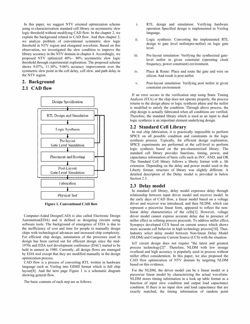
Figure 1. Conventional CAD flow
Computer-Aided Design(CAD) is also called Electronic Design
Automation(EDA) and is defined as designing circuits using software tools. The background of emergence of EDA is due to the inefficiency of cost and time for people to manually design chips with technological advances and increased chip complexity. For efficient chip design, automation of the processes used in design has been carried out for efficient design since the mid-1970s and EDA tool development conference (DAC) started to be held in earnest in 1980. Currently, all design flows are managed by EDA tool except that they are modified manually in the design optimization process.
CAD flow is a process of converting RTL written in hardware language such as Verilog into GDSII format which is full chip layout[8]. And the next page Figure 1 is a schematic diagram showing general flow.
The basic contents of each step are as follows.
i. RTL design and simulation: Verifying hardware operation Specified design is implemented in Verilog language.
ii. Logic synthesis: Converting the implemented RTL design to gate level netlist(pre-netlist) on logic gate level.
iii. Pre-layout simulation: Verifying the synthesized gate-level netlist in given constraint (operating clock frequency, power constraint) environment.
iv. Place & Route: Place and route the gate and wire on silicon. And result is post netlist
v. Post-layout simulation: Verifying post netlist in given constraint environment
If an error occurs in the verification step using Static Timing Analysis (STA) or the chip does not operate properly, the process returns to the design phase or logic synthesis phase and the netlist is modified to satisfy the condition. Through above process, the chip design is actually fabricated when all conditions are verified. Therefore, the standard library which is used as an input to dual logic synthesis is an important element underlying design.
2.2 Standard Cell Library In real chip fabrication, it is practically impossible to perform
SPICE on all possible condition and constraints in the logic synthesis process. Typically, for efficient design exploration, SPICE experiments are performed at the cell-level to perform logic synthesis based on the pre-characterized library. The standard cell library provides functions, timing, power, and capacitance information of basic cells such as INV, AND, and OR. The Standard Cell library follows a liberty format with a .lib extension. Depending on the delay and power model used in the Liberty format, structure of library was slightly different. A detailed description of the Delay model is provided in below Section 2.3.
2.3 Delay model In standard cell library, delay model expresses delay through
relationship between input driver model and receiver model. In the early days of CAD flow, a linear model based on a voltage driver and receiver was introduced, and then NLDM, which can represent a piecewise linear form, appeared to reflect the non-linear delay characteristics of the cells[1]. However, voltage driver model cannot express accurate delay due to presence of miller effect as refining process proceeds. To address miller effect, Synopsys developed CCS based on current source which shows more accurate cell behavior in high technology process[10]. Thus, Industry select delay model between Non-linear Delay Model (NLDM) and Composite Current Source (CCS) with the situation. IoT circuit design does not require "the latest and greatest
process technology[2]". Therefore, NLDM with low storage overhead and high accuracy is popularly used in process without miller effect consideration. In this paper, we also proposed the CAD flow optimization of NTV domain by targeting NLDM based on this evidence.
For the NLDM, the driver model can be a linear model or a piecewise linear model by characterizing the actual waveform. NLDM stores timing information in a look up table format as a function of input slew condition and output load capacitance condition. If there is no input slew and load capacitance that are exactly matched, the timing information of random point
expressed as an approximation of the nearest four points through interpolation. Timing information in NLDM is classified as a transition time
called slew and delay. Delay is a measure of the time that takes for a waveform to propagate within a cell from the input to the output, and slew is a measure of the time that transition is completed when a waveform is transitioned. To quantify these delays and slew, a criterion is needed. In most cases, input and output threshold of delay is set to 50% of the VDD equally. Slew takes symmetrical points based on 50%, utilizes 10%-90%, 30%-70% of VDD in general. Synopsys calls this slew point the slew logic high threshold and the slew logic low threshold[10], and will use that name in the paper.
3. Proposed Method Although industries use different slew logic threshold by
fabrication environments in a typical STV as described in section 2.3, most case use symmetrical 10% -90%, 30% -70% based on 50%. This is because the operating voltage, 1.2V, is enough higher than the threshold voltage of 0.4V, so that sufficient driving strength is maintained during the transition time. However, taking the slew point symmetrically in the NTV environment is not reasonable considering the driving strength.
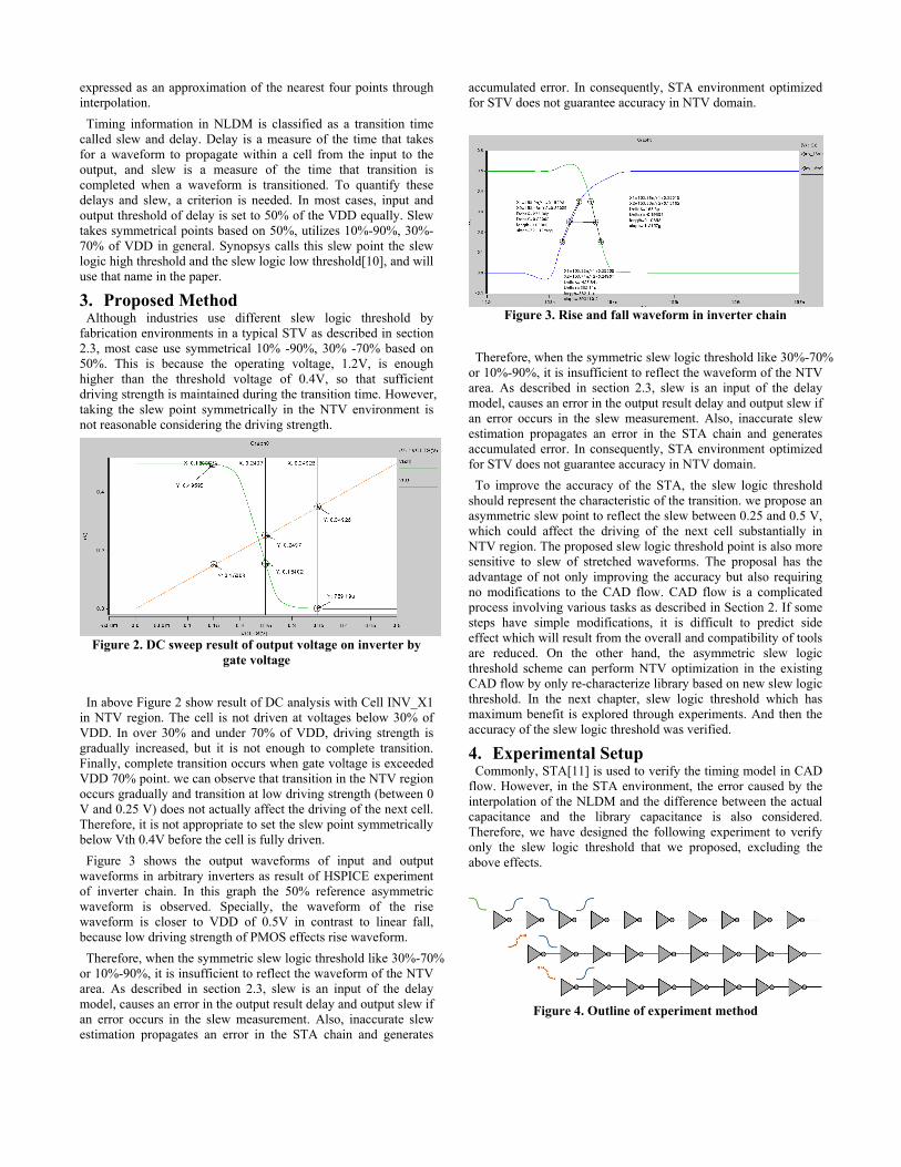
Figure 2. DC sweep result of output voltage on inverter by
gate voltage In above Figure 2 show result of DC analysis with Cell INV_X1
in NTV region. The cell is not driven at voltages below 30% of VDD. In over 30% and under 70% of VDD, driving strength is gradually increased, but it is not enough to complete transition. Finally, complete transition occurs when gate voltage is exceeded VDD 70% point. we can observe that transition in the NTV region occurs gradually and transition at low driving strength (between 0 V and 0.25 V) does not actually affect the driving of the next cell. Therefore, it is not appropriate to set the slew point symmetrically below Vth 0.4V before the cell is fully driven. Figure 3 shows the output waveforms of input and output
waveforms in arbitrary inverters as result of HSPICE experiment of inverter chain. In this graph the 50% reference asymmetric waveform is observed. Specially, the waveform of the rise waveform is closer to VDD of 0.5V in contrast to linear fall, because low driving strength of PMOS effects rise waveform. Therefore, when the symmetric slew logic threshold like 30%-70%
or 10%-90%, it is insufficient to reflect the waveform of the NTV area. As described in section 2.3, slew is an input of the delay model, causes an error in the output result delay and output slew if an error occurs in the slew measurement. Also, inaccurate slew estimation propagates an error in the STA chain and generates
accumulated error. In consequently, STA environment optimized for STV does not guarantee accuracy in NTV domain.
Figure 3. Rise and fall waveform in inverter chain Therefore, when the symmetric slew logic threshold like 30%-70%
or 10%-90%, it is insufficient to reflect the waveform of the NTV area. As described in section 2.3, slew is an input of the delay model, causes an error in the output result delay and output slew if an error occurs in the slew measurement. Also, inaccurate slew estimation propagates an error in the STA chain and generates accumulated error. In consequently, STA environment optimized for STV does not guarantee accuracy in NTV domain. To improve the accuracy of the STA, the slew logic threshold
should represent the characteristic of the transition. we propose an asymmetric slew point to reflect the slew between 0.25 and 0.5 V, which could affect the driving of the next cell substantially in NTV region. The proposed slew logic threshold point is also more sensitive to slew of stretched waveforms. The proposal has the advantage of not only improving the accuracy but also requiring no modifications to the CAD flow. CAD flow is a complicated process involving various tasks as described in Section 2. If some steps have simple modifications, it is difficult to predict side effect which will result from the overall and compatibility of tools are reduced. On the other hand, the asymmetric slew logic threshold scheme can perform NTV optimization in the existing CAD flow by only re-characterize library based on new slew logic threshold. In the next chapter, slew logic threshold which has maximum benefit is explored through experiments. And then the accuracy of the slew logic threshold was verified.
4. Experimental Setup Commonly, STA[11] is used to verify the timing model in CAD
flow. However, in the STA environment, the error caused by the interpolation of the NLDM and the difference between the actual capacitance and the library capacitance is also considered. Therefore, we have designed the following experiment to verify only the slew logic threshold that we proposed, excluding the above effects.
Figure 4. Outline of experiment method

The outline of experiment was described as shown in Figure 4. The experiment is proceeded by each stage separately. First, input slew is inserted in first stage. After stage propagation, measuring the slew point in the output waveform from the stage. And next stage input slew is that is generated by the driver model using result of output slew of previous stage corresponding slew logic threshold. This process is repeated until the final stage. And the delay, slew, and total path delay of each stage are calculated in this procedure. The detail experimental environment is as follows. HSPICE[9]
Version K-2015.06-SP2 was used for the simulation and Samsung 65nm process was used for the model parameter. The initial input of the cell chain was 2e-10 slew using 30%-70% slew logic threshold as a linear driver model with rise and fall. The measured results were compared with the HSPICE simulation result of the 10-stage homogeneous cell chain. There are 7 types of cells used in the experiment and they are listed in the Table 1 below.
Table 1. Cells used in the experiment
Behavior Types Cell Inverting INV_X1, NAND2_X1, NOR2_X1, XOR2_X1
Rise or Fall AND2_X1, BUF_X1, OR2_X1, XOR2_X1
The baseline of slew logic threshold is 30%-70%. To reflect the slew characteristic of the NTV region, the threshold which is 30%-70%, 40%-80%, 50%-90% were explored. In order to observe the effect of the slew range (slew logic high threshold-slew logic low threshold), 40% -90%, 45% -95% were added. And we investigate the influence of the slew logic threshold on the driver model. Two driver models (linear driver model and inverter like piecewise linear driver model) were tested. In case of inverter like piecewise linear driver model, it simulates the rise
and fall waveform of INV_X1 in NTV environment and will be referred to as inverter driver model.
5. Result Figure 5 shows experiment results which contain (a) delay error
of stage, (b) slew error of stage, and (c) total path delay error. In this graph, result is mean error both rise and fall inputs to comprehend the overall trend. We observed that the error decreases as the position of the slew threshold approaches the cell operation threshold voltage. The most improved inverter_40%-80% showed 9.07%, 11.30%, and 9.06% accuracy improvement over conventional linear_30%-70% in stage delay, stage slew, and path delay, respectively. Following sub-chapter, we analyze the effect of driver model and effect of slew range and path behavior.
5.1 Driver model
Figure 6. path delay error rate by input condition
Figure 6 shows path delay error rate by input condition. In this
graph we can identify the characteristic of each driver model. Linear driver model shows high accuracy for fall behavior type, but low accuracy for rise behavior type about 8~16% in
Figure 5. Experiment result of (a) stage delay, (b) stage slew, (c) path delay

conventional linear_30%-70%. This is because its model has limitation that cannot represent a stretched rising waveform which appear in NTV operation cell. Although its limitation, when the asymmetric slew logic threshold is applied, the error rate decreases dramatically to half of the value of result in linear_30%-70% driver model in the linear_40%-90% driver model, respectively. On the other hand, inverter driver model that reflects realistic waveform has high accuracy before applying asymmetric slew logic threshold.
5.2 Path behavior & Slew range
Figure 7. path delay error rate in inverting path behavior type Asymmetric slew logic threshold has a positive effect on inverter
driver model as shown in Figure 7. The error rate of inverting behavior type cells in which rising and falling occur repeatedly is high before applying proposed scheme. By applying the scheme, it is possible to confirm that the error rate decreases in all cases.
Additionally, in Figure 5, as the slew range increases, the phenomenon in which error increases slightly can be observed, because increasing slew range includes region which does not affect the driving of a cell, in the NTV region. Therefore, we can conclude that wide slew range is not appropriate in NTV environment. From the results of section 5.1 & 5.2, we confirmed that the
accuracy increases as the slew logic threshold increases in both driver models. This shows that asymmetric slew logic threshold is effective in NTV environment when using any driver model. Inverter driver model shows low overall error and optimal result is inverter_40%-80% driver model with error rates of 2.06%, 1.97% and 1.38%.
6. Conclusion In this paper, we proposed asymmetric slew logic threshold to
improve the accuracy of CAD flow in NTV area. This scheme suggests the environment which is optimized in NTV region by reflecting range of NTV cell operation. Also, Proposal has advantage that it can be applied without modification of the conventional CAD flow. Experimental results show that the proposed approach achieves a reduction in the error rate of conventional one, stage slew, path delay, 9.07%, 11.30%, and 9.06%, respectively.
Acknowledgements This work has supported by IC design Education Center, Korea. and IT R&D program of MOTIE/KEIT. [10052716, Design technology development of ultra-low voltage operating circuit and IP for smart sensor SoC]
Reference [1] Chung, Eui-Young, et al. "Advanced delay analysis method
for submicron ASIC technology." ASIC Conference and Exhibit, 1992., Proceedings of Fifth Annual IEEE International. IEEE, 1992.
[2] Qu, Gang, and Lin Yuan. "Design THINGS for the Internet of things: an EDA perspective." Proceedings of the 2014 IEEE/ACM International Conference on Computer-Aided Design. IEEE Press, 2014.
[3] Jun, Jaehun, Jaegeun Song, and Chulwoo Kim. "A Near-Threshold Voltage Oriented Digital Cell Library for High-Energy Efficiency and Optimized Performance in 65nm CMOS Process." IEEE Transactions on Circuits and Systems I: Regular Papers (2017).
[4] Conos, Nathaniel A., et al. "Maximizing yield in Near-Threshold Computing under the presence of process variation." Power and Timing Modeling, Optimization and Simulation (PATMOS), 2013 23rd International Workshop on. IEEE, 2013.
[5] Kaul, Himanshu, et al. "Near-threshold voltage (NTV) design—Opportunities and challenges." Design Automation Conference (DAC), 2012 49th ACM/EDAC/IEEE. IEEE, 2012.
[6] Pinckney, Nathaniel, et al. "Near-threshold computing in FinFET technologies: Opportunities for improved voltage scalability." Proceedings of the 53rd Annual Design Automation Conference. ACM, 2016.
[7] Gibiluka, Matheus, et al. "A standard cell characterization flow for non-standard voltage supplies." Integrated Circuits and Systems Design (SBCCI), 2016 29th Symposium on. IEEE, 2016.
[8] Lu, Jianchao, and Baris Taskin. "From RTL to GDSII: An ASIC design course development using Synopsys® University Program." Microelectronic Systems Education (MSE), 2011 IEEE International Conference on. IEEE, 2011.
[9] Synopsys Inc. HSPICE user guide: Basic Simulation and Analysis. 2017
[10] Synopsys Inc. Siliconsmart User guide. 2015. [11] Synopsys Inc. Primetime User guide. 2016. [12] Dreslinski, Ronald G., et al. "Near-threshold computing:
Reclaiming moore's law through energy efficient integrated circuits." Proceedings of the IEEE 98.2 (2010): 253-266.

Authors’ background Your Name Title* Research Field Personal website
Young Min Park PhD candidate Solid State Drive, High performance computing system and CAD flow on near threshold voltage
Kwangsu Kim PhD candidate memory hierarchy, near-data processing as well as ultra-low power computing
Byoung Jin Kim PhD candidate memory architecture
and system-level design
Eui-Young Chung Professor System Architecture, Bio-computing, VLSI Design, computer-aided design with low-power applications, flash memory applications
*This form helps us to understand your paper better, the form itself will not be published.
*Title can be chosen from: master student, Phd candidate, assistant professor, lecture, senior lecture, associate professor, full professor