astronomical observing techniques 2018 lecture 9: silicon
TRANSCRIPT


Content1. Detector Types
2. Crystal Lattices
3. Covalent Bond
4. Electronic Bands
5. Fermi Energy and Fermi Function
6. Electric Conductivity
7. Band Gap and Conduction Band
8. Intrinsic Photoconductors
9. Photo-Current
10. Limitations of Intrinsic Photoconductors
11. Extrinsic Photoconductors
12. Depletion Zone
13. Photodiodes
14. Charge Coupled Devices
15. Readout & Operations
16. Detector Noise
[email protected] Astronomical Observing Techniques 2018, Lecture 9: Detectors 1 2

Modern DetectorsPhoton detectorsResponds to individual photons, releases electrons, X-rays to IRExamples: photoconductors, photodiodes, photoemissive detectors
Thermal detectorsAbsorbs photons, changes temperatures, changes resistance, IR and
sub-mm detectorsExamples: bolometers
Coherent receiversResponds directly to electrical field and preserve phase, mainly used
in the sub-mm and radio regimeExamples: heterodyne receivers
[email protected] Astronomical Observing Techniques 2018, Lecture 9: Detectors 1 3

[email protected] Astronomical Observing Techniques 2018, Lecture 9: Detectors 1 4

Crystal Lattice• crystals: periodic
arrangement of atoms, ions or molecules
• smallest group of atoms that repeats is unit cell
• unit cells repeat at lattice points
• crystal structure and symmetry determine many physical properties purple:Na+, green: Cl-
[email protected] Astronomical Observing Techniques 2018, Lecture 9: Detectors 1 5

Diamond Unit Cell
[email protected] Astronomical Observing Techniques 2018, Lecture 9: Detectors 1 6

Covalent Bond• Elements with 4 e– in valence shell form crystals with diamond
lattice structure (each atom bonds to four neighbors).• Double-bonds between neighbours due to “shared” electrons
[email protected] Astronomical Observing Techniques 2018, Lecture 9: Detectors 1 7

Diamond Lattice with 2 ElementsDiamond lattice not only formed by group IV elements (C, Si, Ge) but also by III-V semiconductors (InSb, GaAs, AlP)
[email protected] Astronomical Observing Techniques 2018, Lecture 9: Detectors 1 8

Electronic States and Bands
Single (Hydrogen) Atom Atoms in crystalWavefunctions Ψ overlapà Energy levels of individual
atoms split due to Pauli principle (avoiding the same quantum states)
à Multiple splitting è “bands”
Astronomical Observing Techniques 2018, Lecture 9: Detectors 1

Electron Energy Levels in Carbon
• possible energy levels of electrons in diamond lattice• Pauli exclusion principle leads to splitting of energy states• electrons in conduction band can move freely
en.wikipedia.org/wiki/Electronic_band_structure
[email protected] Astronomical Observing Techniques 2018, Lecture 9: Detectors 1 10

• Pauli exclusion principle 2 fermions cannot occupy same quantum state; fill up unoccupied quantum states
• Fermi energy EF is energy of highest occupied quantum state in a system of fermions at T = 0K
• Fermi function f(E) is probability that state of energy E is occupied at temperature T; f(EF) = 0.5
Fermi Energy
f E( ) = 11+ e E−EF( )/kT
[email protected] Astronomical Observing Techniques 2018, Lecture 9: Detectors 1 11

Electric ConductivityConductivity requires charge carriers in the conduction band
• Metal: Fermi energy in the middle of conduction band -> free electrons at all temperatures
• Insulator: large band gap and Fermi energy between bands• Semiconductor: narrow band gap and Fermi energy between
bands
Eg
[email protected] Astronomical Observing Techniques 2018, Lecture 9: Detectors 1 12

Bandgap
Overcome bandgap Eg by lifting e– into conduction band: 1. external excitation, e.g. via a photon ßphoton detector2. thermal excitation3. impurities
Eg
[email protected] Astronomical Observing Techniques 2018, Lecture 9: Detectors 1 13

• Number of occupied states in conduction band is given by product of number of possible states Nc in conduction band times the probability f(Ec) that they are occupied
• For silicon, temperature increase of 8K doubles number of electrons in conduction band
Electrons in Conduction Band
n0 = Nc f Ec( )
Nc = 22 meff kT
h2⎛
⎝⎜⎞
⎠⎟
3/2
f Ec( ) = 11+ e Ec−EF( )/kT ≈
Ec−EF>>kTe− Ec−EF( )/kT
[email protected] Astronomical Observing Techniques 2018, Lecture 9: Detectors 1 14

Intrinisic Photo-Conductors: Basic Principle- semi-conductor: few charge carriers à high resistance- charge carriers = electron-hole pairs- photon lifts e- into conduction band- applied electric field drives charges to electrodes
[email protected] Astronomical Observing Techniques 2018, Lecture 9: Detectors 1 15
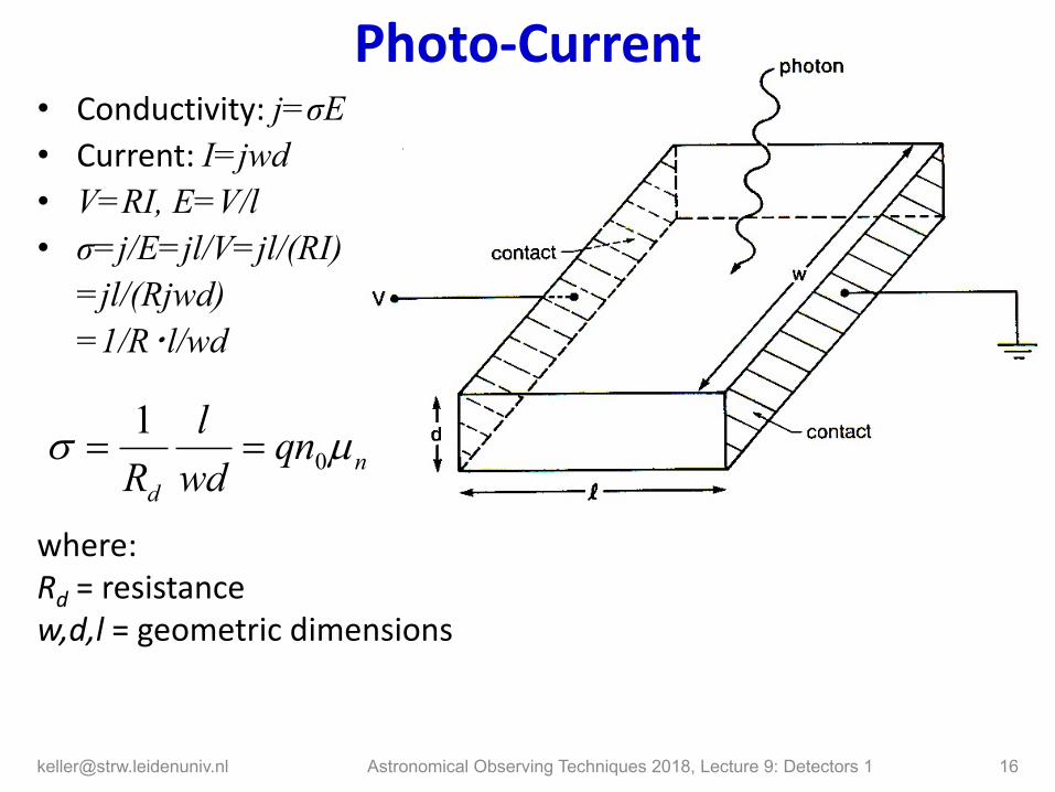
Photo-Current• Conductivity: j=σE• Current: I=jwd• V=RI, E=V/l• σ=j/E=jl/V=jl/(RI)
=jl/(Rjwd)=1/R�l/wd
where:Rd = resistance w,d,l = geometric dimensions
nd
qnwdl
Rµs 0
1==
[email protected] Astronomical Observing Techniques 2018, Lecture 9: Detectors 1 16

Photo-Current
where:Rd = resistance w,d,l = geo. dimensionsq = elementary chargen0 = number density of
charge carriers φ = photon fluxη = quantum efficiencyτ = mean lifetime before recombinationμn = electron mobility; drift velocity v=μnE, current density j=n0qv, σ=j/E=n0qμnE/E=qn0μn
nd
qnwdl
Rµs 0
1==
n0 =ϕητwdl
[email protected] Astronomical Observing Techniques 2018, Lecture 9: Detectors 1 17

Important Quantities and Definitions
electrical output signalResponsivity S =
input photon power
Photoconductive gain G:
The product ηG describes the probability that an incoming photon will produce an electric charge that will reach an electrode
# absorbed photonsQuantum efficiency η =
# incoming photons
metransit tilifetimecarrier
===t
ph
qI
Gtt
jh
Wavelength cutoff:[ ]eVEm
Ehc
ggc
µl 24.1==
Photo-current: GqI ph jh=
[email protected] Astronomical Observing Techniques 2018, Lecture 9: Detectors 1 18

• long-wavelength cutoffs
• difficult to create completely pure material• problems to make good electrical contacts to pure Si• difficult to avoid impurities and minimize thermal
noise
gc Ehc
=lGermanium: 1.85μmSilicon: 1.12μmGaAs: 0.87μm
Limitations of Intrinsic Semiconductors
[email protected] Astronomical Observing Techniques 2018, Lecture 9: Detectors 1 19

Example: addition of boron to silicon in the ratio 1:100,000 increases its conductivity by a factor of 1000!
Extrinsic Semiconductors• extrinsic semiconductors:
charge carriers = electrons (n-type) or holes (p-type)• addition of impurities at low concentration to provide
excess electrons or holes • much reduced bandgap -> longer wavelength cutoff
[email protected] Astronomical Observing Techniques 2018, Lecture 9: Detectors 1 20

Extrinsic Semiconductor Band GapsGe Si
Problem: absorption coefficients much less than for intrinsic photoconductors à low quantum efficiency à active volumes of pixels must be large
[email protected] Astronomical Observing Techniques 2018, Lecture 9: Detectors 1 21

• junction between p- and n-doped Si (both are electrically neutral)• e- migrate to P-side, holes migrate to N-side• e- can only flow over large distances in n-type material, holes can only
flow in p-type material
Depletion Zone / PN Junction
en.wikipedia.org/wiki/Depletion_region
[email protected] Astronomical Observing Techniques 2018, Lecture 9: Detectors 1 22

Depletion Zone / PN Junction• migrating e- from N-side to
P-side produces positive donor ion on N-side; migrating hole produces negative acceptor ion on P-side
• migrating e- recombine with holes on P-side; migrating holes recombine with e- on N-side
• migrating e- and holes, mobile charge carriers are depleted
• charged ions remain adjacent to interface
en.wikipedia.org/wiki/Depletion_region
[email protected] Astronomical Observing Techniques 2018, Lecture 9: Detectors 1 23

Photodiodes• junction between two oppositely doped zones• 2 adjacent zones create a depletion region
1. Photon gets absorbed e.g. in the p-type part2. Absorption creates an e–-hole pair3. The e– diffuses through the material4. Voltage drives the e– across the depletion region à [email protected] Astronomical Observing Techniques 2018, Lecture 9: Detectors 1 24

Charge Coupled Devices (CCDs)CCDs = array of integrating capacitors.Pixel structure: metal “gate” evaporated onto SiO2 (isolator) on silicon = MOS
bias voltage
Vg
1. photons create free e- in the photoconductor2. e– drift toward the electrode but cannot penetrate the SiO2 layer3. e– accumulate at the Si—SiO2 interface4. total charge collected at interface measures number of photons
during the exposure5. à read out the number of e–
[email protected] Astronomical Observing Techniques 2018, Lecture 9: Detectors 1 25

Charge Coupled ReadoutsTi
me
sequ
ence
here: 3 sets of electrodes à 3-phase CCD
Charges are moved along columns to the edge of the array to the output amplifier
Charge transfer (in-)efficiencies (CTEs) due to electrostatic repulsion, thermal diffusion and fringing [email protected] Astronomical Observing Techniques 2018, Lecture 9: Detectors 1 26

http://solar.physics.montana.edu/nuggets/2000/001201/[email protected] Astronomical Observing Techniques 2018, Lecture 9: Detectors 1 27

Charge Transfer Efficiency (CTE)Time-dependent mechanisms that influence the CTE:
1. Electrostatic repulsion causes electrons to drift to the neighbouring electrode with time constant for charge transfer τSI.
2. Thermal diffusion drives electrons across the storage well at τth.
3. “Fringing fields” due to dependency of the well on the voltages of neighbouring electrodes (τff).
( )mteCTE t/1 --=Approximation for the CTE of a CCD with m phases:
Noise from charge transfer inefficiency: ε = (1-CTE)
[email protected] Astronomical Observing Techniques 2018, Lecture 9: Detectors 1 28

CCD Color Sensors1. Three exposures through 3 filters – only works for fixed targets2. Split input into 3 channels with separate filter and CCD3. Bayer mask over CCD – each subset of 4 pixels has one filtered
red, one blue, and two green
[email protected] Astronomical Observing Techniques 2018, Lecture 9: Detectors 1 29

Fundamental thermodynamic noise due to thermal motion of charge carriers. Photo-conductor is an RC circuit where <Q2> = kTC
G-R noise
Johnson or kTC noise
1/f noise
Fundamental statistical noise due to the Poisson statistics of the photon arrival àtransferred into the statistics of the generated and recombined holes and electrons
Main Detector Noise Components
ffII f Dµ2
2/1
fRkTIJ D=42
fGqI RG D=-222 4 jh
increased noise at low frequencies, due to bad electrical contacts, temperature fluctuations, surface effects (damage), crystal defects, and JFETs, …
Total noise: 2/1
222fJRGN IIII ++= -
[email protected] Astronomical Observing Techniques 2018, Lecture 9: Detectors 1 30

Operationally, background-limited performance (BLIP) is always preferred:
The noise equivalent power (NEP) is the signal power that yields an RMS S/N of unity in a system of Δf = 1 Hz:
In BLIP the NEP can only be improved by increasing the quantum efficiency η as background photon noise dominates
2/1
22fJRG III +>>-
2/12
÷÷ø
öççè
æ=- h
jlhcNEP RG
BLIP and NEP
[email protected] Astronomical Observing Techniques 2018, Lecture 9: Detectors 1 31