asmm-cx03-xxxxx plcc-2 surface mount led data sheet...broadcom - 3 - asmm-cx03-xxxxx data sheet...
TRANSCRIPT
ASMM-Cx03-xxxxxPLCC-2 Surface Mount LED
Data Sheet
DescriptionThe ASMM-Cx03 Surface Mount LED is packaged in the industry-standard PLCC-2 package and has high reliability performance designed to work under a wide range of environmental conditions. This high reliability feature makes them ideally suited to be used for wide range of applications.
The wide viewing angle at 120° makes these LEDs ideally suited for panel, push button, or general backlighting in office equipment, industrial equipment, and home appliances. The flat top emitting surface makes it easy for these LEDs to integrate with light pipes. With the built-in reflector enhancing the light output intensity, these LEDs are also suitable to be used as LED pixels in indoor electronic signs.
To facilitate easy pick and place assembly, the LEDs are packed in tape and feel form. Every reel is shipped in single intensity and color bin to provide close uniformity.
Features Industry-standard PLCC-2 package. High reliability LED package with enhanced silicone resin
encapsulation. High brightness using AlGaAs, GaP and AllnGaP dice
technologies. Available in full selection of colors. Wide angle viewing angle at 120°. JEDEC MSL 3.
Applications Electronic signs and signals. Office automations, home appliances, industrial
equipment.— Front panel backlighting— Push button backlighting— Display backlighting— Scanner lighting
Broadcom- 1 -
CAUTION This LED is ESD sensitive. Please observe appropriate precautions during handling and processing. Refer to application note AN-1142 for additional details.
ASMM-Cx03-xxxxx Data Sheet
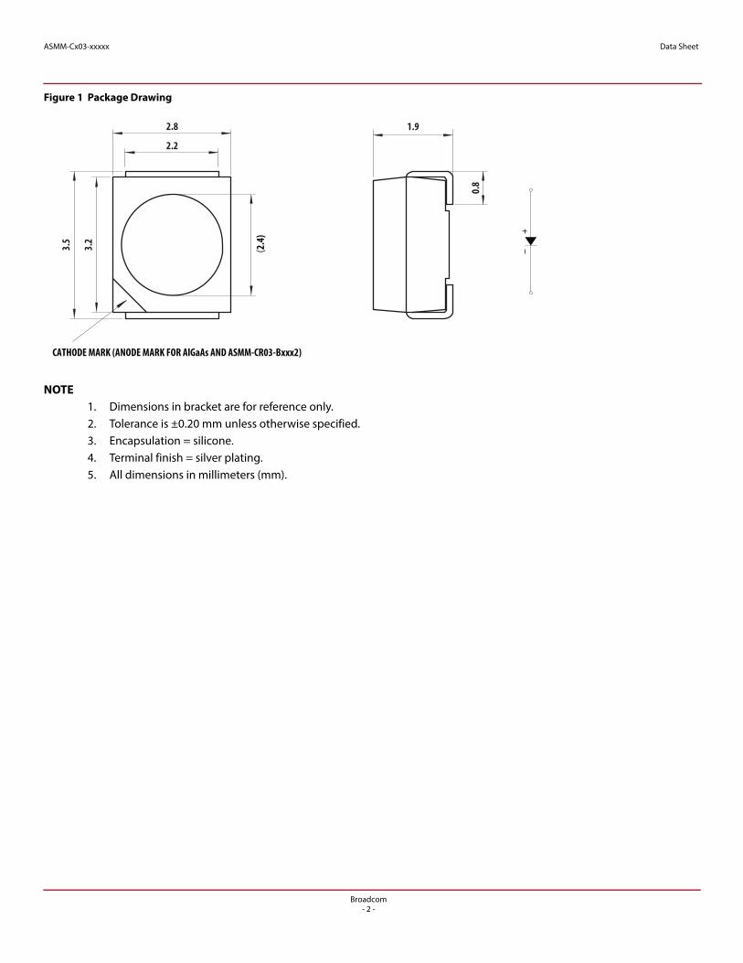
Figure 1 Package Drawing
NOTE1. Dimensions in bracket are for reference only. 2. Tolerance is ±0.20 mm unless otherwise specified.3. Encapsulation = silicone.4. Terminal finish = silver plating.5. All dimensions in millimeters (mm).
3.5
3.2
2.8
2.2
0.8
CATHODE MARK (ANODE MARK FOR AlGaAs AND ASMM-CR03-Bxxx2)
(2.4
)
1.9
Broadcom- 2 -
ASMM-Cx03-xxxxx Data Sheet
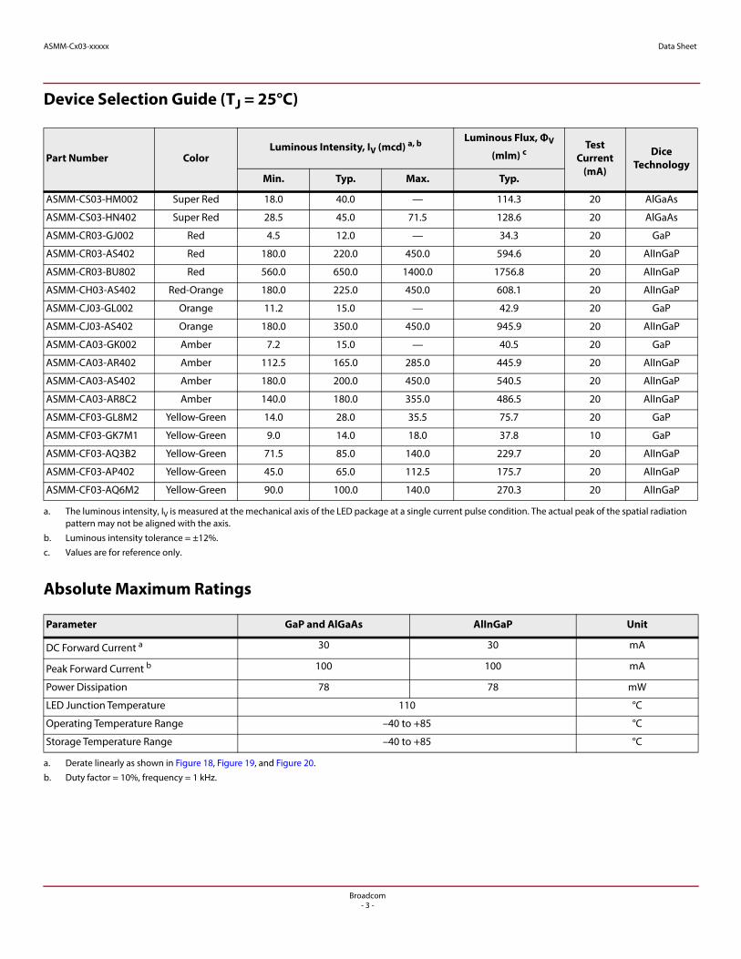
Device Selection Guide (TJ = 25°C)
Absolute Maximum Ratings
Part Number ColorLuminous Intensity, IV (mcd) a, b
a. The luminous intensity, IV is measured at the mechanical axis of the LED package at a single current pulse condition. The actual peak of the spatial radiation pattern may not be aligned with the axis.
b. Luminous intensity tolerance = ±12%.
Luminous Flux, ΦV
(mlm) c
c. Values are for reference only.
Test Current
(mA)
Dice Technology
Min. Typ. Max. Typ.
ASMM-CS03-HM002 Super Red 18.0 40.0 — 114.3 20 AlGaAs
ASMM-CS03-HN402 Super Red 28.5 45.0 71.5 128.6 20 AlGaAs
ASMM-CR03-GJ002 Red 4.5 12.0 — 34.3 20 GaP
ASMM-CR03-AS402 Red 180.0 220.0 450.0 594.6 20 AlInGaP
ASMM-CR03-BU802 Red 560.0 650.0 1400.0 1756.8 20 AlInGaP
ASMM-CH03-AS402 Red-Orange 180.0 225.0 450.0 608.1 20 AlInGaP
ASMM-CJ03-GL002 Orange 11.2 15.0 — 42.9 20 GaP
ASMM-CJ03-AS402 Orange 180.0 350.0 450.0 945.9 20 AlInGaP
ASMM-CA03-GK002 Amber 7.2 15.0 — 40.5 20 GaP
ASMM-CA03-AR402 Amber 112.5 165.0 285.0 445.9 20 AlInGaP
ASMM-CA03-AS402 Amber 180.0 200.0 450.0 540.5 20 AlInGaP
ASMM-CA03-AR8C2 Amber 140.0 180.0 355.0 486.5 20 AlInGaP
ASMM-CF03-GL8M2 Yellow-Green 14.0 28.0 35.5 75.7 20 GaP
ASMM-CF03-GK7M1 Yellow-Green 9.0 14.0 18.0 37.8 10 GaP
ASMM-CF03-AQ3B2 Yellow-Green 71.5 85.0 140.0 229.7 20 AlInGaP
ASMM-CF03-AP402 Yellow-Green 45.0 65.0 112.5 175.7 20 AlInGaP
ASMM-CF03-AQ6M2 Yellow-Green 90.0 100.0 140.0 270.3 20 AlInGaP
Parameter GaP and AlGaAs AlInGaP Unit
DC Forward Current a
a. Derate linearly as shown in Figure 18, Figure 19, and Figure 20.
30 30 mA
Peak Forward Current b
b. Duty factor = 10%, frequency = 1 kHz.
100 100 mA
Power Dissipation 78 78 mW
LED Junction Temperature 110 °C
Operating Temperature Range –40 to +85 °C
Storage Temperature Range –40 to +85 °C
Broadcom- 3 -
ASMM-Cx03-xxxxx Data Sheet
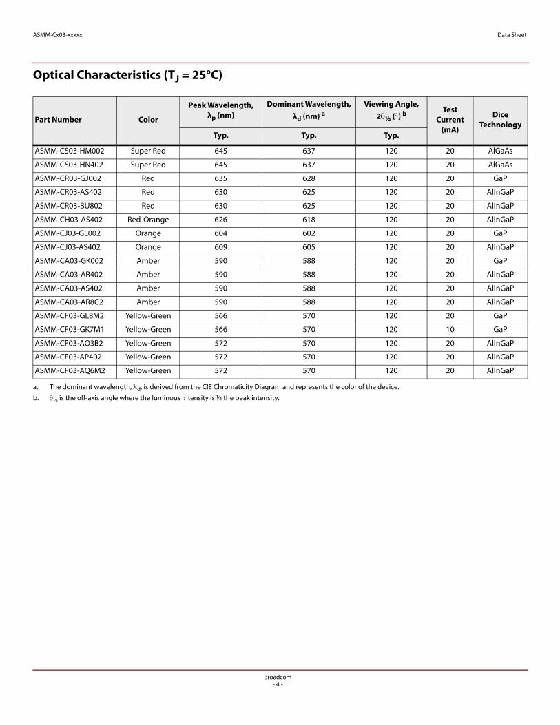
Optical Characteristics (TJ = 25°C)
Part Number Color
Peak Wavelength, λp (nm)
Dominant Wavelength, λd (nm) a
a. The dominant wavelength, d, is derived from the CIE Chromaticity Diagram and represents the color of the device.
Viewing Angle, 2½ () b
b. ½ is the off-axis angle where the luminous intensity is ½ the peak intensity.
Test Current
(mA)
Dice Technology
Typ. Typ. Typ.
ASMM-CS03-HM002 Super Red 645 637 120 20 AlGaAs
ASMM-CS03-HN402 Super Red 645 637 120 20 AlGaAs
ASMM-CR03-GJ002 Red 635 628 120 20 GaP
ASMM-CR03-AS402 Red 630 625 120 20 AlInGaP
ASMM-CR03-BU802 Red 630 625 120 20 AlInGaP
ASMM-CH03-AS402 Red-Orange 626 618 120 20 AlInGaP
ASMM-CJ03-GL002 Orange 604 602 120 20 GaP
ASMM-CJ03-AS402 Orange 609 605 120 20 AlInGaP
ASMM-CA03-GK002 Amber 590 588 120 20 GaP
ASMM-CA03-AR402 Amber 590 588 120 20 AlInGaP
ASMM-CA03-AS402 Amber 590 588 120 20 AlInGaP
ASMM-CA03-AR8C2 Amber 590 588 120 20 AlInGaP
ASMM-CF03-GL8M2 Yellow-Green 566 570 120 20 GaP
ASMM-CF03-GK7M1 Yellow-Green 566 570 120 10 GaP
ASMM-CF03-AQ3B2 Yellow-Green 572 570 120 20 AlInGaP
ASMM-CF03-AP402 Yellow-Green 572 570 120 20 AlInGaP
ASMM-CF03-AQ6M2 Yellow-Green 572 570 120 20 AlInGaP
Broadcom- 4 -
ASMM-Cx03-xxxxx Data Sheet
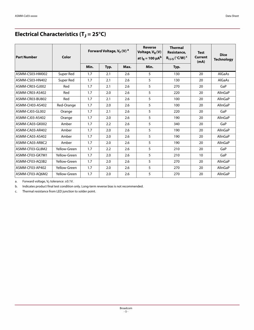
Electrical Characteristics (TJ = 25°C)
Part Number Color
Forward Voltage, VF (V) a
a. Forward voltage, VF tolerance: ±0.1V.
Reverse Voltage, VR (V)
at IR = 100 μAb
b. Indicates product final test condition only. Long-term reverse bias is not recommended.
Thermal Resistance,
RJ-S (C/W) c
c. Thermal resistance from LED junction to solder point.
Test Current
(mA)
Dice Technology
Min. Typ. Max. Min. Typ.
ASMM-CS03-HM002 Super Red 1.7 2.1 2.6 5 130 20 AlGaAs
ASMM-CS03-HN402 Super Red 1.7 2.1 2.6 5 130 20 AlGaAs
ASMM-CR03-GJ002 Red 1.7 2.1 2.6 5 270 20 GaP
ASMM-CR03-AS402 Red 1.7 2.0 2.6 5 220 20 AlInGaP
ASMM-CR03-BU802 Red 1.7 2.1 2.6 5 100 20 AlInGaP
ASMM-CH03-AS402 Red-Orange 1.7 2.0 2.6 5 100 20 AlInGaP
ASMM-CJ03-GL002 Orange 1.7 2.1 2.6 5 220 20 GaP
ASMM-CJ03-AS402 Orange 1.7 2.0 2.6 5 190 20 AlInGaP
ASMM-CA03-GK002 Amber 1.7 2.2 2.6 5 340 20 GaP
ASMM-CA03-AR402 Amber 1.7 2.0 2.6 5 190 20 AlInGaP
ASMM-CA03-AS402 Amber 1.7 2.0 2.6 5 190 20 AlInGaP
ASMM-CA03-AR8C2 Amber 1.7 2.0 2.6 5 190 20 AlInGaP
ASMM-CF03-GL8M2 Yellow-Green 1.7 2.2 2.6 5 210 20 GaP
ASMM-CF03-GK7M1 Yellow-Green 1.7 2.0 2.6 5 210 10 GaP
ASMM-CF03-AQ3B2 Yellow-Green 1.7 2.0 2.6 5 270 20 AlInGaP
ASMM-CF03-AP402 Yellow-Green 1.7 2.0 2.6 5 270 20 AlInGaP
ASMM-CF03-AQ6M2 Yellow-Green 1.7 2.0 2.6 5 270 20 AlInGaP
Broadcom- 5 -
ASMM-Cx03-xxxxx Data Sheet
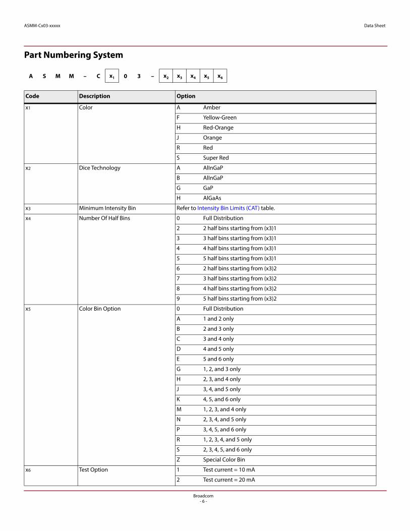
Part Numbering System
A S M M – C x1 0 3 – x2 x3 x4 x5 x6
Code Description Option
x1 Color A Amber
F Yellow-Green
H Red-Orange
J Orange
R Red
S Super Red
x2 Dice Technology A AlInGaP
B AlInGaP
G GaP
H AlGaAs
x3 Minimum Intensity Bin Refer to Intensity Bin Limits (CAT) table.
x4 Number Of Half Bins 0 Full Distribution
2 2 half bins starting from (x3)1
3 3 half bins starting from (x3)1
4 4 half bins starting from (x3)1
5 5 half bins starting from (x3)1
6 2 half bins starting from (x3)2
7 3 half bins starting from (x3)2
8 4 half bins starting from (x3)2
9 5 half bins starting from (x3)2
x5 Color Bin Option 0 Full Distribution
A 1 and 2 only
B 2 and 3 only
C 3 and 4 only
D 4 and 5 only
E 5 and 6 only
G 1, 2, and 3 only
H 2, 3, and 4 only
J 3, 4, and 5 only
K 4, 5, and 6 only
M 1, 2, 3, and 4 only
N 2, 3, 4, and 5 only
P 3, 4, 5, and 6 only
R 1, 2, 3, 4, and 5 only
S 2, 3, 4, 5, and 6 only
Z Special Color Bin
x6 Test Option 1 Test current = 10 mA
2 Test current = 20 mA
Broadcom- 6 -
ASMM-Cx03-xxxxx Data Sheet
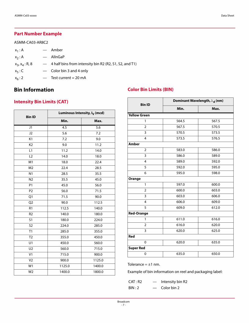
Part Number Example
ASMM-CA03-AR8C2
x1 : A — Amber
x2 : A — AlInGaP
x3, x4 : R, 8 — 4 half bins from intensity bin R2 (R2, S1, S2, and T1)
x5 : C — Color bin 3 and 4 only
x6 : 2 — Test current = 20 mA
Bin Information
Intensity Bin Limits (CAT)
Color Bin Limits (BIN)
Tolerance = ±1 nm.
Example of bin information on reel and packaging label:
Bin IDLuminous Intensity, IV (mcd)
Min. Max.
J1 4.5 5.6
J2 5.6 7.2
K1 7.2 9.0
K2 9.0 11.2
L1 11.2 14.0
L2 14.0 18.0
M1 18.0 22.4
M2 22.4 28.5
N1 28.5 35.5
N2 35.5 45.0
P1 45.0 56.0
P2 56.0 71.5
Q1 71.5 90.0
Q2 90.0 112.5
R1 112.5 140.0
R2 140.0 180.0
S1 180.0 224.0
S2 224.0 285.0
T1 285.0 355.0
T2 355.0 450.0
U1 450.0 560.0
U2 560.0 715.0
V1 715.0 900.0
V2 900.0 1125.0
W1 1125.0 1400.0
W2 1400.0 1800.0
Bin IDDominant Wavelength, d (nm)
Min. Max.
Yellow Green
1 564.5 567.5
2 567.5 570.5
3 570.5 573.5
4 573.5 576.5
Amber
2 583.0 586.0
3 586.0 589.0
4 589.0 592.0
5 592.0 595.0
6 595.0 598.0
Orange
1 597.0 600.0
2 600.0 603.0
3 603.0 606.0
4 606.0 609.0
5 609.0 612.0
Red-Orange
1 611.0 616.0
2 616.0 620.0
3 620.0 625.0
Red
0 620.0 635.0
Super Red
0 635.0 650.0
CAT : R2 — Intensity bin R2
BIN : 2 — Color bin 2
Broadcom- 7 -
ASMM-Cx03-xxxxx Data Sheet
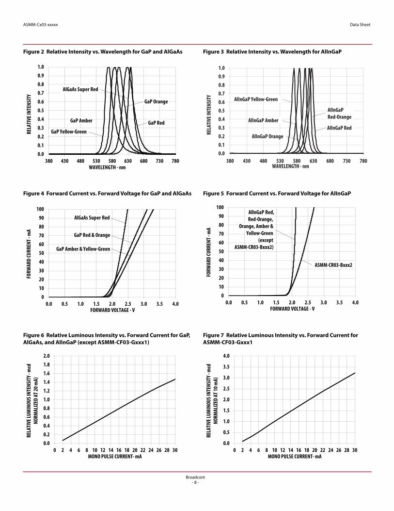
Figure 2 Relative Intensity vs. Wavelength for GaP and AlGaAs Figure 3 Relative Intensity vs. Wavelength for AlInGaP
0.0
0.1
0.2
0.3
0.4
0.5
0.6
0.7
0.8
0.9
1.0
380 430 480 530 580 630 680 730 780
REL
ATI
VE
INTE
NSI
TY
WAVELENGTH - nm
AlGaAs Super Red
GaP Red
GaP Orange
GaP Yellow-Green
GaP Amber
0.00.10.20.30.40.50.60.70.80.91.0
380 430 480 530 580 630 680 730 780
RELA
TIVE
INTE
NSIT
Y
WAVELENGTH - nm
AlInGaP Red
AlInGaP Red-Orange AlInGaP Amber
AlInGaP Orange
AlInGaP Yellow-Green
Figure 4 Forward Current vs. Forward Voltage for GaP and AlGaAs Figure 5 Forward Current vs. Forward Voltage for AlInGaP
0
10
20
30
40
50
60
70
80
90
100
0.0 0.5 1.0 1.5 2.0 2.5 3.0 3.5 4.0
FOR
WA
RD
CU
RR
ENT
-mA
FORWARD VOLTAGE - V
GaP Red & Orange
GaP Amber & Yellow-Green
AlGaAs Super Red
0
10
20
30
40
50
60
70
80
90
100
0.0 0.5 1.0 1.5 2.0 2.5 3.0 3.5 4.0
FOR
WA
RD
CU
RR
ENT
-mA
FORWARD VOLTAGE - V
AllnGaP Red,
Red-Orange,
Orange, Amber &
Yellow-Green
(except
ASMM-CR03-Bxxx2)
ASMM-CR03-Bxxx2
Figure 6 Relative Luminous Intensity vs. Forward Current for GaP, AlGaAs, and AlInGaP (except ASMM-CF03-Gxxx1)
Figure 7 Relative Luminous Intensity vs. Forward Current for ASMM-CF03-Gxxx1
0.0
0.2
0.4
0.6
0.8
1.0
1.2
1.4
1.6
1.8
2.0
0 2 4 6 8 10 12 14 16 18 20 22 24 26 28 30
REL
ATI
VE L
UM
INO
US
INTE
NSI
TY -
mcd
NO
RM
ALI
ZED
AT
20 m
A)
MONO PULSE CURRENT- mA
0.0
0.5
1.0
1.5
2.0
2.5
3.0
3.5
4.0
0 2 4 6 8 10 12 14 16 18 20 22 24 26 28 30
REL
ATI
VE L
UM
INO
US
INTE
NSI
TY -
mcd
NO
RM
ALI
ZED
AT
10 m
A)
MONO PULSE CURRENT- mA
Broadcom- 8 -
ASMM-Cx03-xxxxx Data Sheet
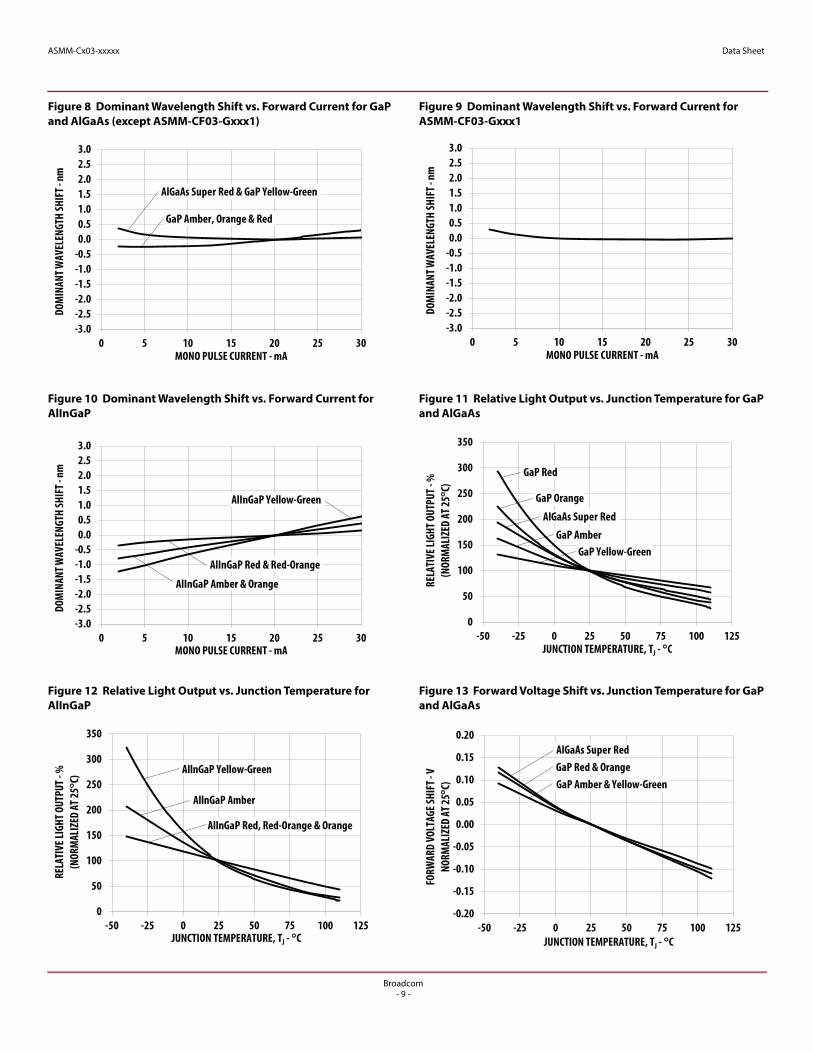
Figure 8 Dominant Wavelength Shift vs. Forward Current for GaP and AlGaAs (except ASMM-CF03-Gxxx1)
Figure 9 Dominant Wavelength Shift vs. Forward Current for ASMM-CF03-Gxxx1
-3.0
-2.5
-2.0
-1.5
-1.0
-0.5
0.0
0.5
1.0
1.5
2.0
2.5
3.0
0 5 10 15 20 25 30
DO
MIN
AN
T W
AV
ELEN
GTH
SH
IFT
-nm
MONO PULSE CURRENT - mA
AlGaAs Super Red & GaP Yellow-Green
GaP Amber, Orange & Red
-3.0
-2.5
-2.0
-1.5
-1.0
-0.5
0.0
0.5
1.0
1.5
2.0
2.5
3.0
0 5 10 15 20 25 30
DO
MIN
AN
T W
AVE
LEN
GTH
SH
IFT
-nm
MONO PULSE CURRENT - mA
Figure 10 Dominant Wavelength Shift vs. Forward Current for AlInGaP
Figure 11 Relative Light Output vs. Junction Temperature for GaP and AlGaAs
-3.0
-2.5
-2.0
-1.5
-1.0
-0.5
0.0
0.5
1.0
1.5
2.0
2.5
3.0
0 5 10 15 20 25 30
DO
MIN
AN
T W
AV
ELEN
GTH
SH
IFT
-nm
MONO PULSE CURRENT - mA
AlInGaP Amber & Orange
AlInGaP Red & Red-Orange
AlInGaP Yellow-Green
0
50
100
150
200
250
300
350
-50 -25 0 25 50 75 100 125
REL
ATI
VE L
IGH
T O
UTP
UT
-%
(NO
RM
ALI
ZED
AT
25C)
JUNCTION TEMPERATURE, TJ - C
GaP Red
GaP Orange
AlGaAs Super Red
GaP Amber
GaP Yellow-Green
Figure 12 Relative Light Output vs. Junction Temperature for AlInGaP
Figure 13 Forward Voltage Shift vs. Junction Temperature for GaP and AlGaAs
0
50
100
150
200
250
300
350
-50 -25 0 25 50 75 100 125
REL
ATI
VE
LIG
HT
OU
TPU
T -%
(NO
RM
ALI
ZED
AT
25C)
JUNCTION TEMPERATURE, TJ - C
AllnGaP Red, Red-Orange & Orange
AllnGaP Amber
AllnGaP Yellow-Green
-0.20
-0.15
-0.10
-0.05
0.00
0.05
0.10
0.15
0.20
-50 -25 0 25 50 75 100 125
FOR
WA
RD
VO
LTA
GE
SHIF
T -V
NO
RM
ALI
ZED
AT
25C)
JUNCTION TEMPERATURE, TJ - C
AlGaAs Super Red
GaP Red & Orange
GaP Amber & Yellow-Green
Broadcom- 9 -
ASMM-Cx03-xxxxx Data Sheet
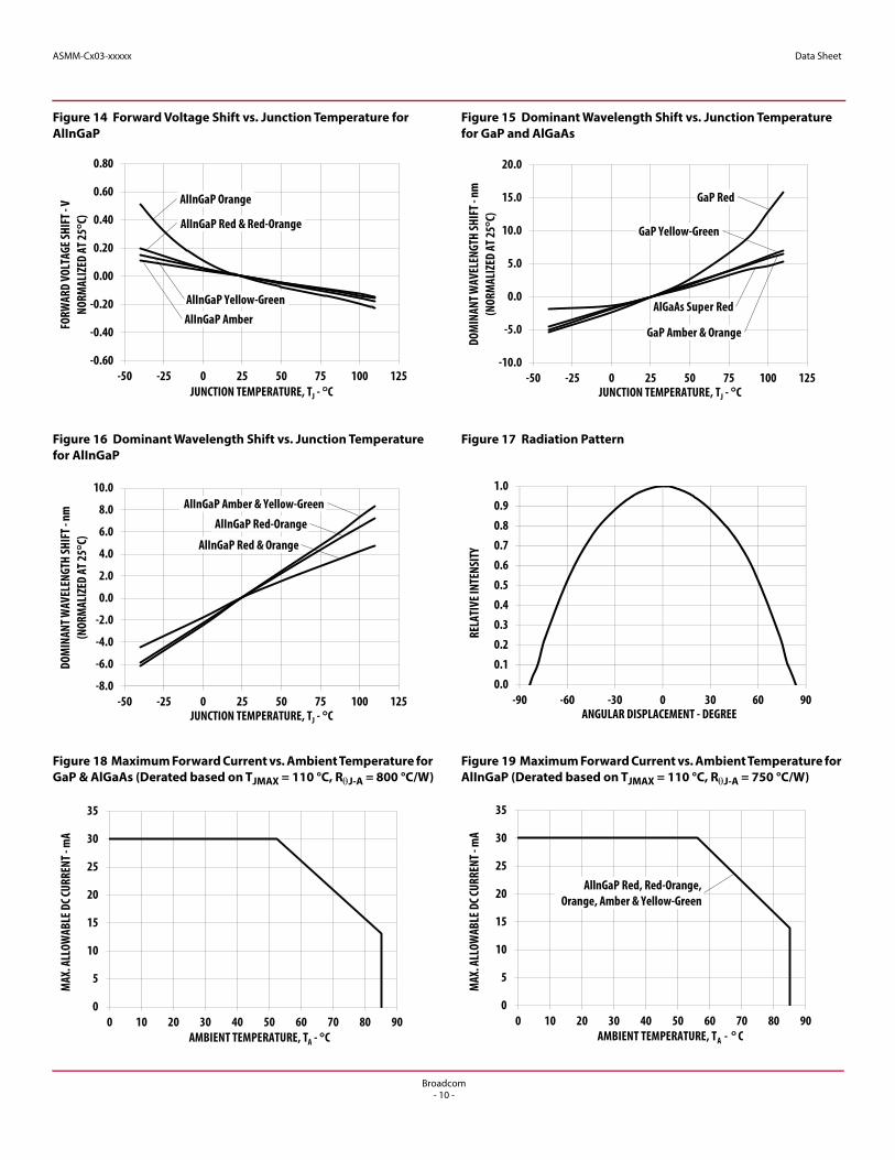
Figure 14 Forward Voltage Shift vs. Junction Temperature for AlInGaP
Figure 15 Dominant Wavelength Shift vs. Junction Temperature for GaP and AlGaAs
-0.60
-0.40
-0.20
0.00
0.20
0.40
0.60
0.80
-50 -25 0 25 50 75 100 125
FOR
WA
RD
VO
LTA
GE
SHIF
T -V
NO
RM
ALI
ZED
AT
25C)
JUNCTION TEMPERATURE, TJ - C
AlInGaP Orange
AlInGaP Amber
AlInGaP Red & Red-Orange
AlInGaP Yellow-Green
-10.0
-5.0
0.0
5.0
10.0
15.0
20.0
-50 -25 0 25 50 75 100 125
DO
MIN
AN
T W
AV
ELEN
GTH
SH
IFT
-nm
(NO
RM
ALI
ZED
AT
25C)
JUNCTION TEMPERATURE, TJ - C
GaP Red
GaP Yellow-Green
GaP Amber & Orange
AlGaAs Super Red
Figure 16 Dominant Wavelength Shift vs. Junction Temperature for AlInGaP
Figure 17 Radiation Pattern
-8.0
-6.0
-4.0
-2.0
0.0
2.0
4.0
6.0
8.0
10.0
-50 -25 0 25 50 75 100 125
DO
MIN
AN
T W
AV
ELEN
GTH
SH
IFT
-nm
(NO
RM
ALI
ZED
AT
25C)
JUNCTION TEMPERATURE, TJ - C
AlInGaP Amber & Yellow-Green
AlInGaP Red-Orange
AlInGaP Red & Orange
0.0
0.1
0.2
0.3
0.4
0.5
0.6
0.7
0.8
0.9
1.0
-90 -60 -30 0 30 60 90
REL
ATI
VE
INTE
NSI
TY
ANGULAR DISPLACEMENT - DEGREE
Figure 18 Maximum Forward Current vs. Ambient Temperature for GaP & AlGaAs (Derated based on TJMAX = 110 °C, RJ-A = 800 °C/W)
Figure 19 Maximum Forward Current vs. Ambient Temperature for AlInGaP (Derated based on TJMAX = 110 °C, RJ-A = 750 °C/W)
0
5
10
15
20
25
30
35
0 10 20 30 40 50 60 70 80 90
MAX
. ALL
OWAB
LE D
C CUR
RENT
-mA
AMBIENT TEMPERATURE, TA - C
0
5
10
15
20
25
30
35
0 10 20 30 40 50 60 70 80 90
MAX
. ALL
OWAB
LE D
C CUR
RENT
-mA
AMBIENT TEMPERATURE, TA - C
AllnGaP Red, Red-Orange,Orange, Amber & Yellow-Green
Broadcom- 10 -
ASMM-Cx03-xxxxx Data Sheet
Figure 20 Maximum Forward Current vs. Solder Point Temperature (Derated based on TJMAX = 110 °C)
Figure 21 Recommended Soldering Pad Pattern
0
5
10
15
20
25
30
35
0 10 20 30 40 50 60 70 80 90
MA
X. A
LLO
WA
BLE
DC
CUR
REN
T -m
A
SOLDER POINT TEMPERATURE, TS - C
NOTE All dimensions are in millimeters.
4.5
1.5
2.6
Figure 22 Carrier Tape Dimensions
NOTE All dimensions are in millimeters.
3.8 ± 0.1
2.29 ± 0.1
0.229 ± 0.01
2 ± 0.054 ± 0.1 4 ± 0.1
3.05 ± 0.1
3.5 ± 0.05
8 +0.3–0.1
1.75 ± 0.1Ø1.5
+0.1–0
8°
Ø1+0.1–0
A
C
USER FEED DIRECTION
Broadcom- 11 -
ASMM-Cx03-xxxxx Data Sheet
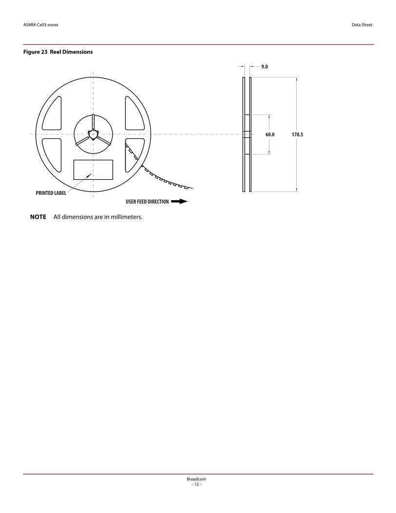
Figure 23 Reel Dimensions
NOTE All dimensions are in millimeters.
178.560.0
USER FEED DIRECTION
PRINTED LABEL
9.0
Broadcom- 12 -
ASMM-Cx03-xxxxx Data Sheet
Precautionary Notes
Soldering
Do not perform reflow soldering more than twice. Observe necessary precautions of handling moisture-sensitive device as stated in the following section.
Do not apply any pressure or force on the LED during reflow and after reflow when the LED is still hot.
Use reflow soldering to solder the LED. Use hand soldering only for rework if unavoidable, but it must be strictly controlled to following conditions:— Soldering iron tip temperature = 315°C max.— Soldering duration = 3 sec max.— Number of cycles = 1 only.— Power of soldering iron = 50W max.
Do not touch the LED package body with the soldering iron except for the soldering terminals, as it may cause damage to the LED.
Confirm beforehand whether the functionality and performance of the LED is affected by soldering with hand soldering.
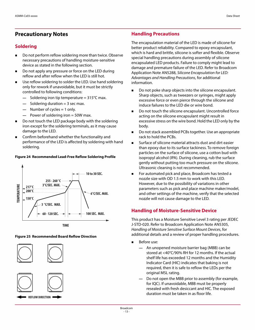
Figure 24 Recommended Lead-Free Reflow Soldering Profile
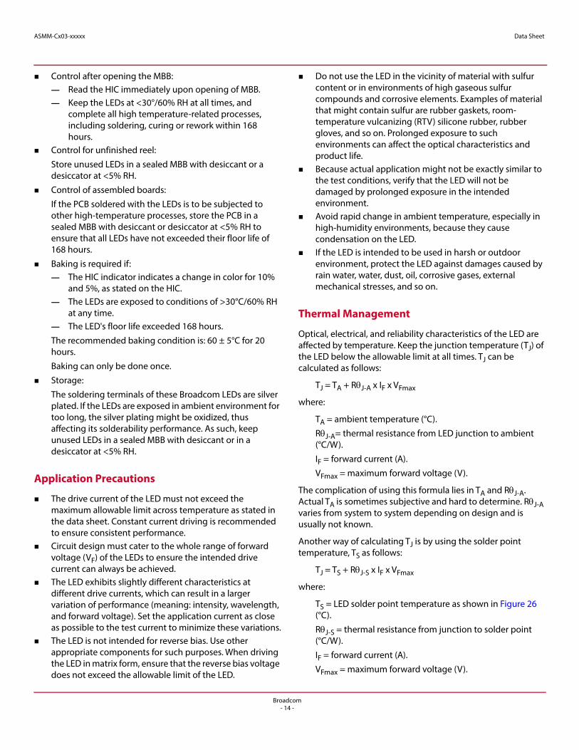
Figure 25 Recommended Board Reflow Direction
Handling Precautions
The encapsulation material of the LED is made of silicone for better product reliability. Compared to epoxy encapsulant, which is hard and brittle, silicone is softer and flexible. Observe special handling precautions during assembly of silicone encapsulated LED products. Failure to comply might lead to damage and premature failure of the LED. Refer to Broadcom Application Note AN5288, Silicone Encapsulation for LED: Advantages and Handling Precautions, for additional information.
Do not poke sharp objects into the silicone encapsulant. Sharp objects, such as tweezers or syringes, might apply excessive force or even pierce through the silicone and induce failures to the LED die or wire bond.
Do not touch the silicone encapsulant. Uncontrolled force acting on the silicone encapsulant might result in excessive stress on the wire bond. Hold the LED only by the body.
Do not stack assembled PCBs together. Use an appropriate rack to hold the PCBs.
Surface of silicone material attracts dust and dirt easier than epoxy due to its surface tackiness. To remove foreign particles on the surface of silicone, use a cotton bud with isopropyl alcohol (IPA). During cleaning, rub the surface gently without putting too much pressure on the silicone. Ultrasonic cleaning is not recommended.
For automated pick and place, Broadcom has tested a nozzle size with OD 1.5 mm to work with this LED. However, due to the possibility of variations in other parameters such as pick and place machine maker/model, and other settings of the machine, verify that the selected nozzle will not cause damage to the LED.
Handling of Moisture-Sensitive Device
This product has a Moisture Sensitive Level 3 rating per JEDEC J-STD-020. Refer to Broadcom Application Note AN5305, Handling of Moisture Sensitive Surface Mount Devices, for additional details and a review of proper handling procedures.
Before use:— An unopened moisture barrier bag (MBB) can be
stored at <40°C/90% RH for 12 months. If the actual shelf life has exceeded 12 months and the Humidity Indicator Card (HIC) indicates that baking is not required, then it is safe to reflow the LEDs per the original MSL rating.
— Do not open the MBB prior to assembly (for example, for IQC). If unavoidable, MBB must be properly resealed with fresh desiccant and HIC. The exposed duration must be taken in as floor life.
217 °C200 °C
60 - 120 SEC.
6°C/SEC. MAX.
3 °C/SEC. MAX.
3 °C/SEC. MAX.
150 °C
255 - 260 °C
100 SEC. MAX.
10 to 30 SEC.
TIME
TEM
PER
ATU
RE
REFLOW DIRECTION
Broadcom- 13 -
ASMM-Cx03-xxxxx Data Sheet
Control after opening the MBB:— Read the HIC immediately upon opening of MBB.— Keep the LEDs at <30°/60% RH at all times, and
complete all high temperature-related processes, including soldering, curing or rework within 168 hours.
Control for unfinished reel:
Store unused LEDs in a sealed MBB with desiccant or a desiccator at <5% RH.
Control of assembled boards:
If the PCB soldered with the LEDs is to be subjected to other high-temperature processes, store the PCB in a sealed MBB with desiccant or desiccator at <5% RH to ensure that all LEDs have not exceeded their floor life of 168 hours.
Baking is required if:— The HIC indicator indicates a change in color for 10%
and 5%, as stated on the HIC.— The LEDs are exposed to conditions of >30°C/60% RH
at any time.— The LED's floor life exceeded 168 hours.
The recommended baking condition is: 60 ± 5°C for 20 hours.
Baking can only be done once.
Storage:
The soldering terminals of these Broadcom LEDs are silver plated. If the LEDs are exposed in ambient environment for too long, the silver plating might be oxidized, thus affecting its solderability performance. As such, keep unused LEDs in a sealed MBB with desiccant or in a desiccator at <5% RH.
Application Precautions
The drive current of the LED must not exceed the maximum allowable limit across temperature as stated in the data sheet. Constant current driving is recommended to ensure consistent performance.
Circuit design must cater to the whole range of forward voltage (VF) of the LEDs to ensure the intended drive current can always be achieved.
The LED exhibits slightly different characteristics at different drive currents, which can result in a larger variation of performance (meaning: intensity, wavelength, and forward voltage). Set the application current as close as possible to the test current to minimize these variations.
The LED is not intended for reverse bias. Use other appropriate components for such purposes. When driving the LED in matrix form, ensure that the reverse bias voltage does not exceed the allowable limit of the LED.
Do not use the LED in the vicinity of material with sulfur content or in environments of high gaseous sulfur compounds and corrosive elements. Examples of material that might contain sulfur are rubber gaskets, room- temperature vulcanizing (RTV) silicone rubber, rubber gloves, and so on. Prolonged exposure to such environments can affect the optical characteristics and product life.
Because actual application might not be exactly similar to the test conditions, verify that the LED will not be damaged by prolonged exposure in the intended environment.
Avoid rapid change in ambient temperature, especially in high-humidity environments, because they cause condensation on the LED.
If the LED is intended to be used in harsh or outdoor environment, protect the LED against damages caused by rain water, water, dust, oil, corrosive gases, external mechanical stresses, and so on.
Thermal Management
Optical, electrical, and reliability characteristics of the LED are affected by temperature. Keep the junction temperature (TJ) of the LED below the allowable limit at all times. TJ can be calculated as follows:
TJ = TA + RJ-A x IF x VFmax
where:
TA = ambient temperature (°C).
RJ-A= thermal resistance from LED junction to ambient (°C/W).
IF = forward current (A).
VFmax = maximum forward voltage (V).
The complication of using this formula lies in TA and RJ-A. Actual TA is sometimes subjective and hard to determine. RJ-A varies from system to system depending on design and is usually not known.
Another way of calculating TJ is by using the solder point temperature, TS as follows:
TJ = TS + RJ-S x IF x VFmax
where:
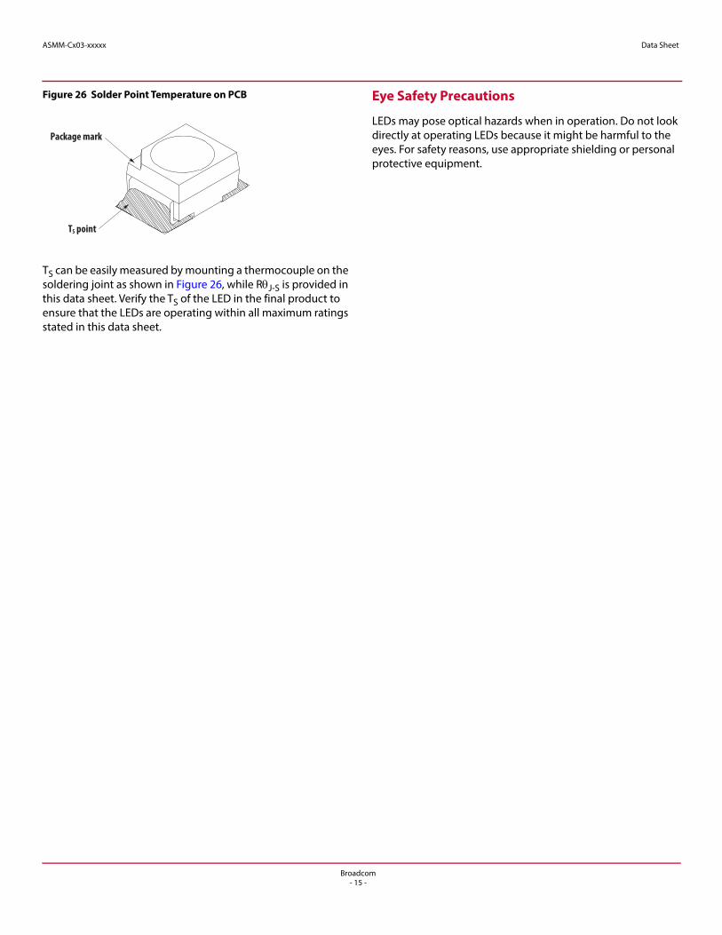
TS = LED solder point temperature as shown in Figure 26 (°C).
RJ-S = thermal resistance from junction to solder point (°C/W).
IF = forward current (A).
VFmax = maximum forward voltage (V).
Broadcom- 14 -
ASMM-Cx03-xxxxx Data Sheet
Figure 26 Solder Point Temperature on PCB
TS can be easily measured by mounting a thermocouple on the soldering joint as shown in Figure 26, while RJ-S is provided in this data sheet. Verify the TS of the LED in the final product to ensure that the LEDs are operating within all maximum ratings stated in this data sheet.
Eye Safety Precautions
LEDs may pose optical hazards when in operation. Do not look directly at operating LEDs because it might be harmful to the eyes. For safety reasons, use appropriate shielding or personal protective equipment.
Package mark
TS point
Broadcom- 15 -
Disclaimer
Broadcom's products and software are not specifically designed, manufactured, or authorized for sale as parts, components, or assemblies for the planning, construction, maintenance, or direct operation of a nuclear facility or for use in medical devices or applications. The customer is solely responsible, and waives all rights to make claims against Broadcom or its suppliers, for all loss, damage, expense, or liability in connection with such use.
For product information and a complete list of distributors, please go to our web site: www.broadcom.com.
Broadcom, the pulse logo, Connecting everything, Avago Technologies, Avago, and the A logo are among the trademarks of Broadcom in the United States, certain other countries and/or the EU.
Copyright © 2017–2018 Broadcom. All Rights Reserved.
The term "Broadcom" refers to Broadcom Limited and/or its subsidiaries. For more information, please visit www.broadcom.com.
Broadcom reserves the right to make changes without further notice to any products or data herein to improve reliability, function, or design.
Information furnished by Broadcom is believed to be accurate and reliable. However, Broadcom does not assume any liability arising out of the application or use of this information, nor the application or use of any product or circuit described herein, neither does it convey any license under its patent rights nor the rights of others.
ASMM-Cx03-xxxxx-DS101 – March 16, 2018