asic/fpga chip design - sharif university of...
TRANSCRIPT

//ASIC/FPGA CASIC/FPGA C
Power DiPower Di
Mahdi
D t t f ElDepartment of Ele
Sharif Universi
© M. Shabany, ASIC/F
Chip DesignChip Design
ssipationssipation
Shabany
t i l E i iectrical Engineering
ity of technology
FPGA Chip Design
Outline
• Introductionoduc o
• Dynamic Power Dissipation
• Static Power Dissipationp
© M. Shabany, ASIC/FFPGA Chip Design 2

Outline
• Introductionoduc o
• Dynamic Power Dissipation
• Static Power Dissipationp
© M. Shabany, ASIC/FFPGA Chip Design 3
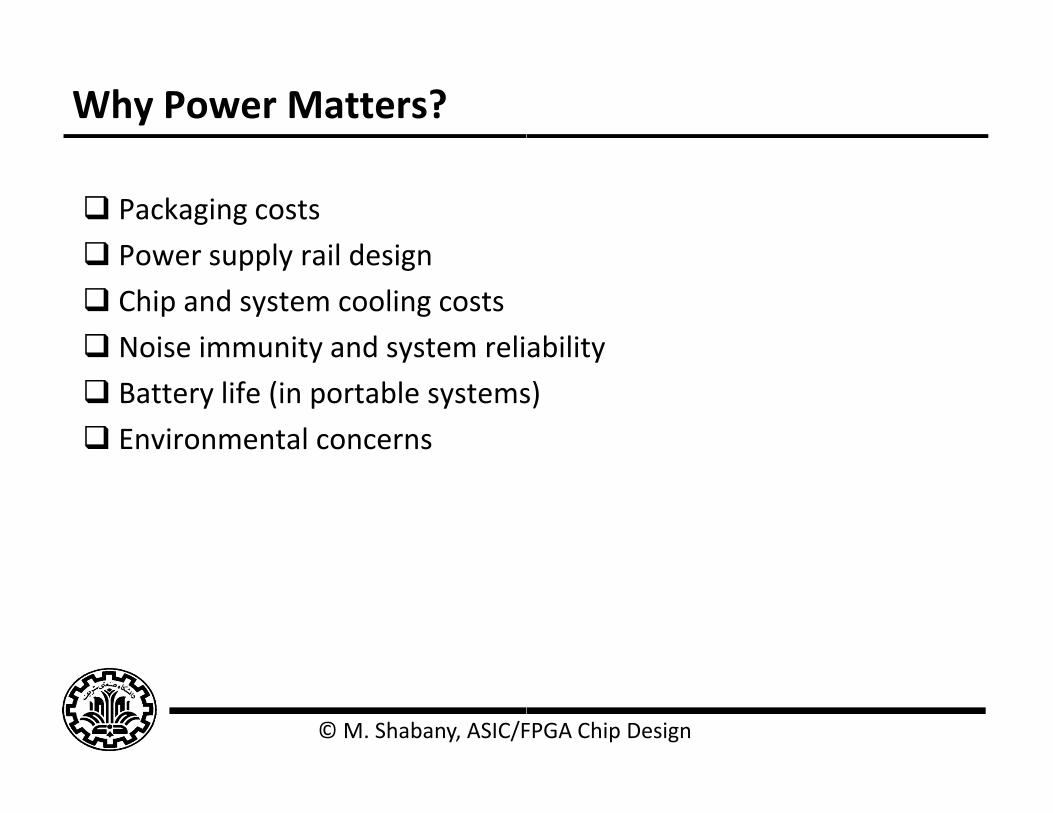
Why Power Matters?
Packaging costs
Power supply rail design Power supply rail design
Chip and system cooling costs
Noise immunity and system reli Noise immunity and system reli
Battery life (in portable systems
Environmental concerns
© M. Shabany, ASIC/F
abilityability
s)
FPGA Chip Design
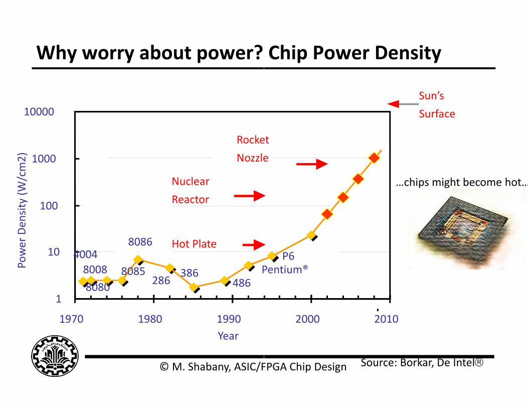
Why worry about power?
10000
1000
/cm2)
N l
Rocke
Nozzle
100
Den
sity (W
/ Nuclear
Reactor
40048008 8085
8086
286386
486P
10
Power D
Hot Plate
8080 286 4861
1970 1980 1990Y
© M. Shabany, ASIC/F
Year
Chip Power Density
Sun’s
Surface
et
e
hi i h b h…chips might become hot…
Pentium®P6
2000 2010
FPGA Chip Design Source: Borkar, De Intel
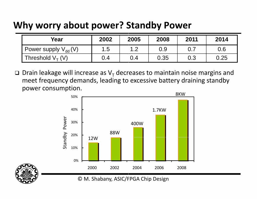
Why worry about power? SYear 2002 2
Power supply Vdd (V) 1.5Threshold VT (V) 0.4
Drain leakage will increase as VT decrmeet frequency demands, leading topower consumptionpower consumption.
40%
50%
88W 12W
20%
30%
by Pow
er
12W
0%
10%Stand
© M. Shabany, ASIC/F
2000 2002
Standby Power 2005 2008 2011 20141.2 0.9 0.7 0.60.4 0.35 0.3 0.25
reases to maintain noise margins and excessive battery draining standby
8KW
1.7KW
400W
FPGA Chip Design
2004 2006 2008
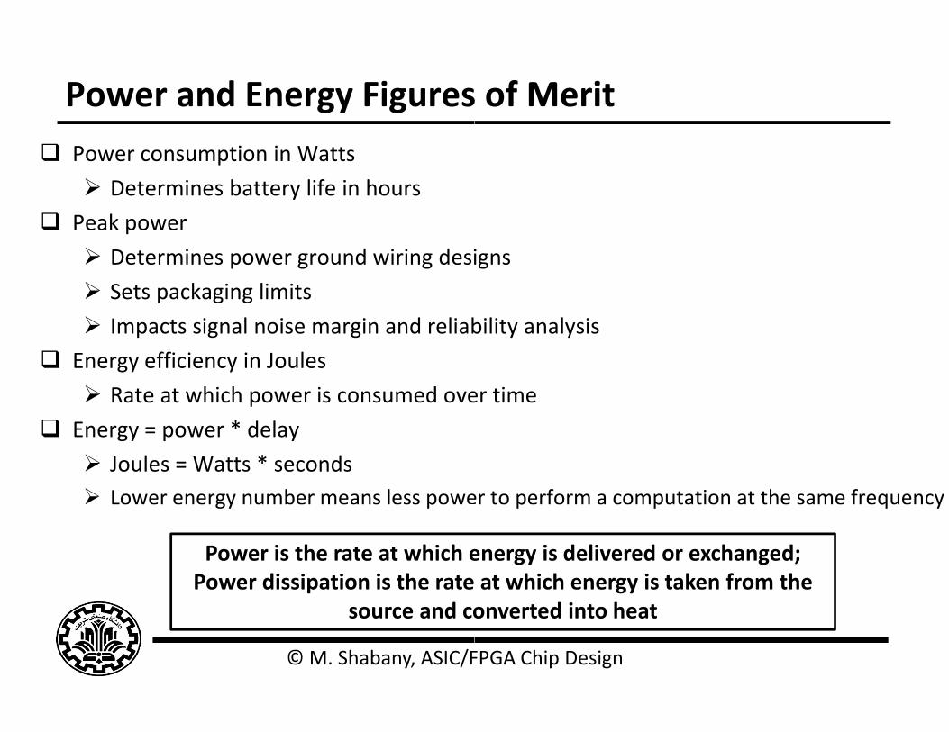
Power and Energy Figures Power consumption in Watts
Determines battery life in hours
Peak power Peak power
Determines power ground wiring desi
Sets packaging limits
I t i l i i d li b Impacts signal noise margin and reliab
Energy efficiency in Joules
Rate at which power is consumed ove
Energy = power * delay
Joules = Watts * seconds Lower energy number means less powegy p
Power is the rate at which ePower dissipation is the rate
© M. Shabany, ASIC/F
source and co
s of Merit
igns
bilit l ibility analysis
er time
er to perform a computation at the same frequencyp p q y
energy is delivered or exchanged; at which energy is taken from the
FPGA Chip Design
onverted into heat
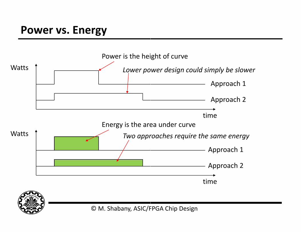
Power vs. Energy
Watts
Power is the hei
Lower poLower po
Energy is the areWatts Two appr
© M. Shabany, ASIC/F
ight of curve
ower design could simply be slower
Approach 1
Approach 2
ower design could simply be slower
time
Approach 2
ea under curve
Approach 1
roaches require the same energy
time
Approach 2
FPGA Chip Design
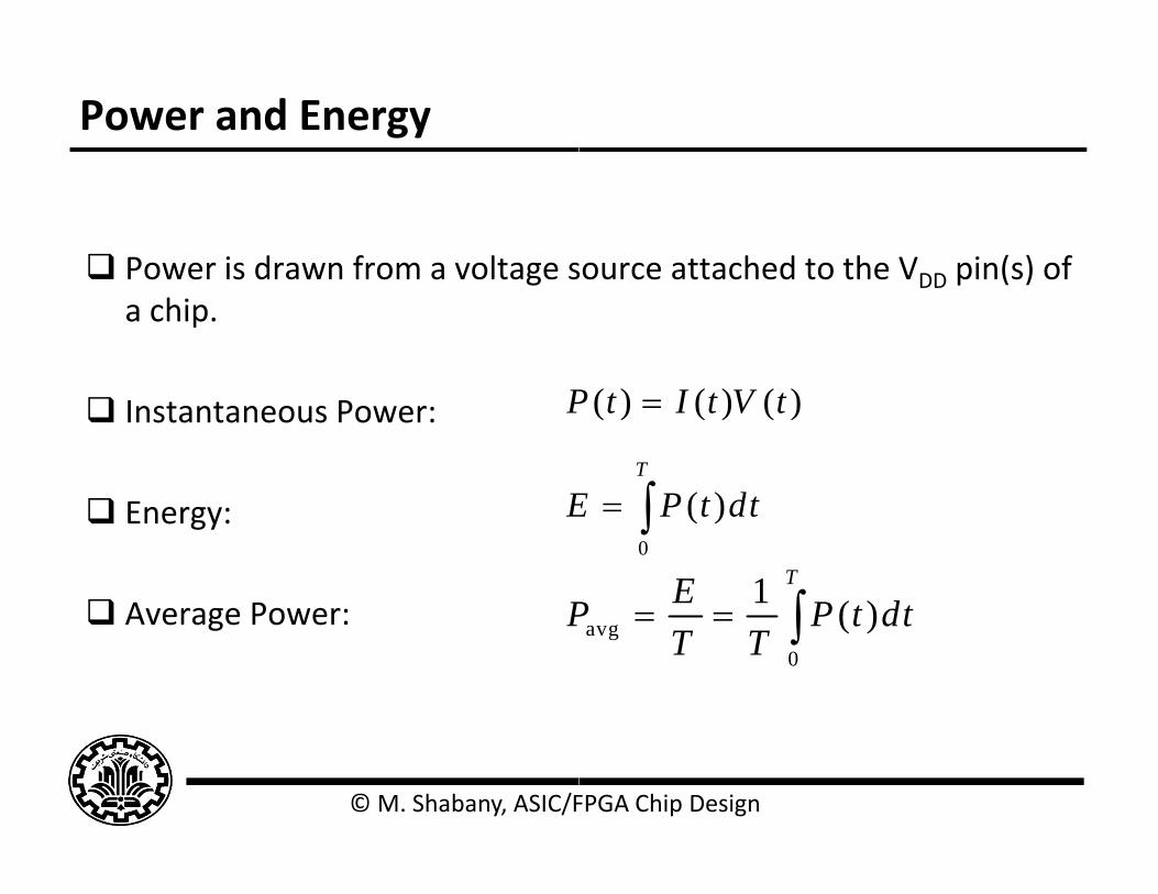
Power and Energy
Power is drawn from a voltage s Power is drawn from a voltage sa chip.
P Instantaneous Power:
E
P
E Energy:
Average Power:
E
P Average Power: P
© M. Shabany, ASIC/F
source attached to the VDD pin(s) ofsource attached to the VDD pin(s) of
( ) ( ) ( )P I V( ) ( ) ( )P t I t V t
( )T
E P t dt 0
( )E P t dt 1 ( )
TEP P t dt avg0
( )P P t dtT T
FPGA Chip Design
Power in Circuit Elements
VDD DD DDP t I t V
2
2
2RR R
V tP t I t R
R
0 0
CdVE I t V t dt C V t dtdt
212
0
CV
CC V t dV CV
© M. Shabany, ASIC/FFPGA Chip Design

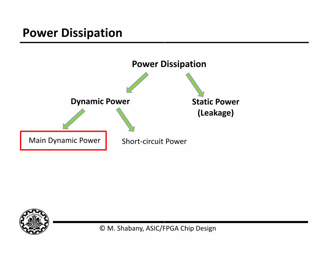
Power Dissipation Power: Due to the current flowing f
DVIP
Power Dissipation:
DVIP
Dynamic Power : Occurs only when t Charging/discharging of load capaci Short‐circuit power during switching
Static Power: Due to the presence of a In CMOS, when circuit is quiescent (ideally no current flows through an Othus zero static power
© M. Shabany, ASIC/F
rom supply to ground
DDVDDV
he gate switchestancesg (when both NMOS and PMOS are ON)
a path in the gate b/w the power supply & GND(no switching) one of the transistors is OFF thus
/FF transistor so no current b/w VDD and GND
FPGA Chip Design

Power Dissipation
Power D
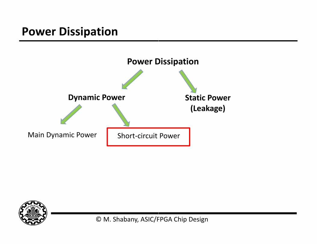
Dynamic Power
Short‐circuit Main Dynamic Power
© M. Shabany, ASIC/F
Dissipation
Static Power(L k )
Power
(Leakage)
FPGA Chip Design

CMOS Total Energy & Powe
E = CL VDD2 α01 + α sL DD 01 s
ff01
C 2 f
Dynamic Power Short
P = CL VDD2 f01 + α s
Dynamic Power Short
(~90% today and decreasing relatively)
(~8da
© M. Shabany, ASIC/F
relatively) a
er Equations
sc VDD2 CL + VDD Istaticsc DD L DD static
* f= α01 * fClk
2 C f
circuit Power Static Power
c VDD2 CL fClk + VDD Istatic
‐circuit Power Static Power
8% today and decreasing absolutely)
(~2% today and increasing)
FPGA Chip Design
absolutely)

Outline
• Introductionoduc o
• Dynamic Power Dissipation
• Static Power Dissipationp
© M. Shabany, ASIC/FFPGA Chip Design 14
Power Dissipation
Power D
Dynamic Power
Short‐circuitMain Dynamic Power Short circuit y
© M. Shabany, ASIC/F
Dissipation
Static Power(L k )
Power
(Leakage)
Power
FPGA Chip Design
Power Dissipation: Main D Due to the charging/discharging the load
dtv(t)i(t)T1
PT
0avg
dV)(
1 T/2out
dt
dt
dV)C(V
T1
P0
outLoutavg
2T/22 VV1 2out
0
L
2out
avg 2
V‐C
2
V
T1
P
© M. Shabany, ASIC/F
Dynamic Powerd capacitances
Vout
VDD
T/2 T
)dV
(T
out
dt)
dt
dV(‐CV
T/2
outLout
T1
Clk2DDLL
2DD
T/2
L fVCCVT1
C
FPGA Chip Design
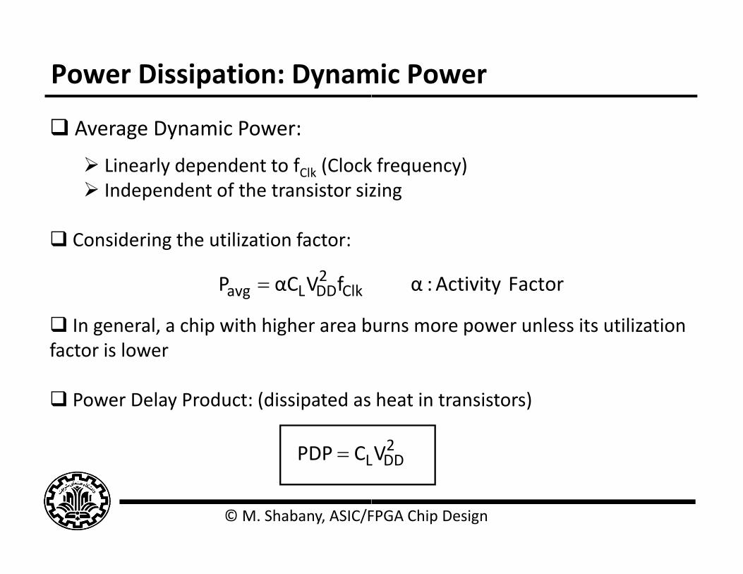
Power Dissipation: Dynam
Average Dynamic Power:
Linearly dependent to fClk (Clock Independent of the transistor siz
Considering the utilization factor:
In general a chip with higher area b
fVαCP Clk2DDLavg
In general, a chip with higher area bfactor is lower
P D l P d t (di i t d Power Delay Product: (dissipated as
LCPDP
© M. Shabany, ASIC/F
mic Power
k frequency)zing
urns more power unless its utilization
Factor Activity :α
urns more power unless its utilization
h t i t i t )heat in transistors)
2DDLV
FPGA Chip Design
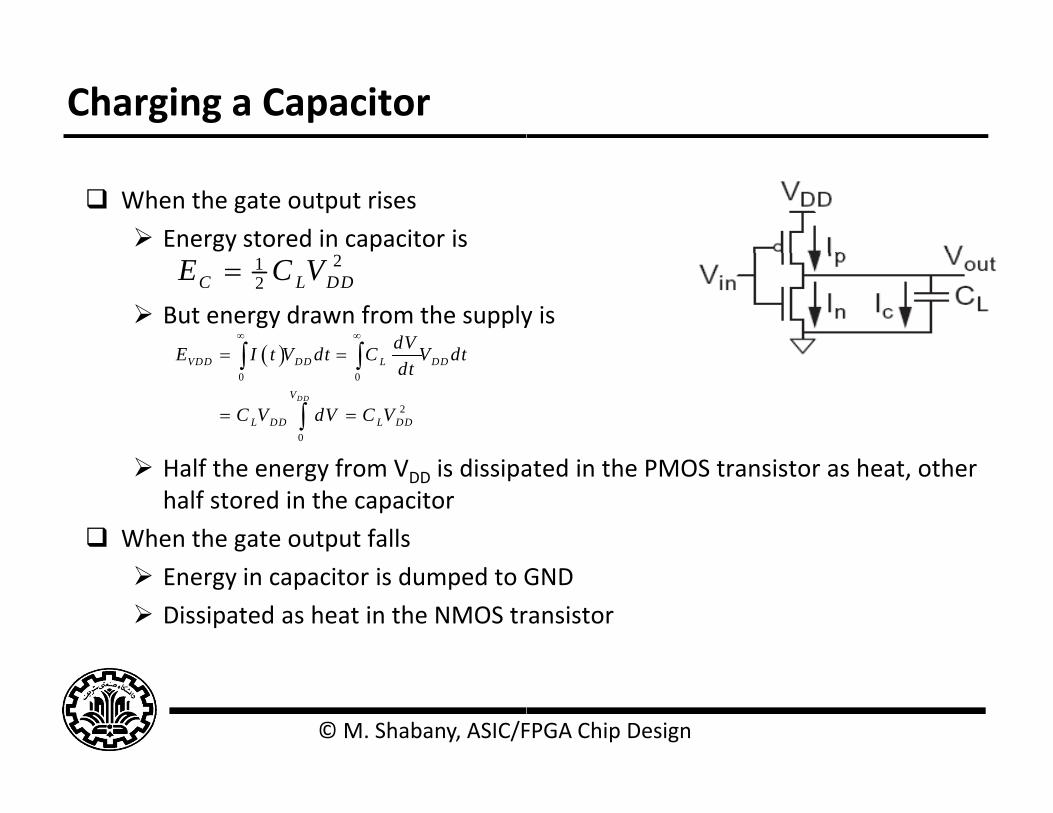
Charging a Capacitor
When the gate output rises
Energy stored in capacitor is
But energy drawn from the supply
212C L DDE C V
dVE I t V dt C V dt
0 0
2
0
DD
VDD DD L DD
V
L DD L DD
E I t V dt C V dtdt
C V dV C V
Half the energy from VDD is dissipahalf stored in the capacitor
When the gate output falls
Energy in capacitor is dumped to G
Dissipated as heat in the NMOS tr
© M. Shabany, ASIC/F
y is
ated in the PMOS transistor as heat, other
GND
ransistor
FPGA Chip Design

Dynamic Power Consumpt
Energy/transition =gy/
Pdyn = Energy/transition *
Pdyn = Ceff * VDD2 * fPdyn Ceff VDD f
Not a function of transistor Data dependent ‐ a function
© M. Shabany, ASIC/F
Data dependent a function
tion
= CL * VDD2 * α01
f01
L DD 01
* f = CL * VDD2 * α01 * f
where Ceff = α01 CL where Ceff α01 CL
sizes!n of switching activity!
FPGA Chip Design
n of switching activity!
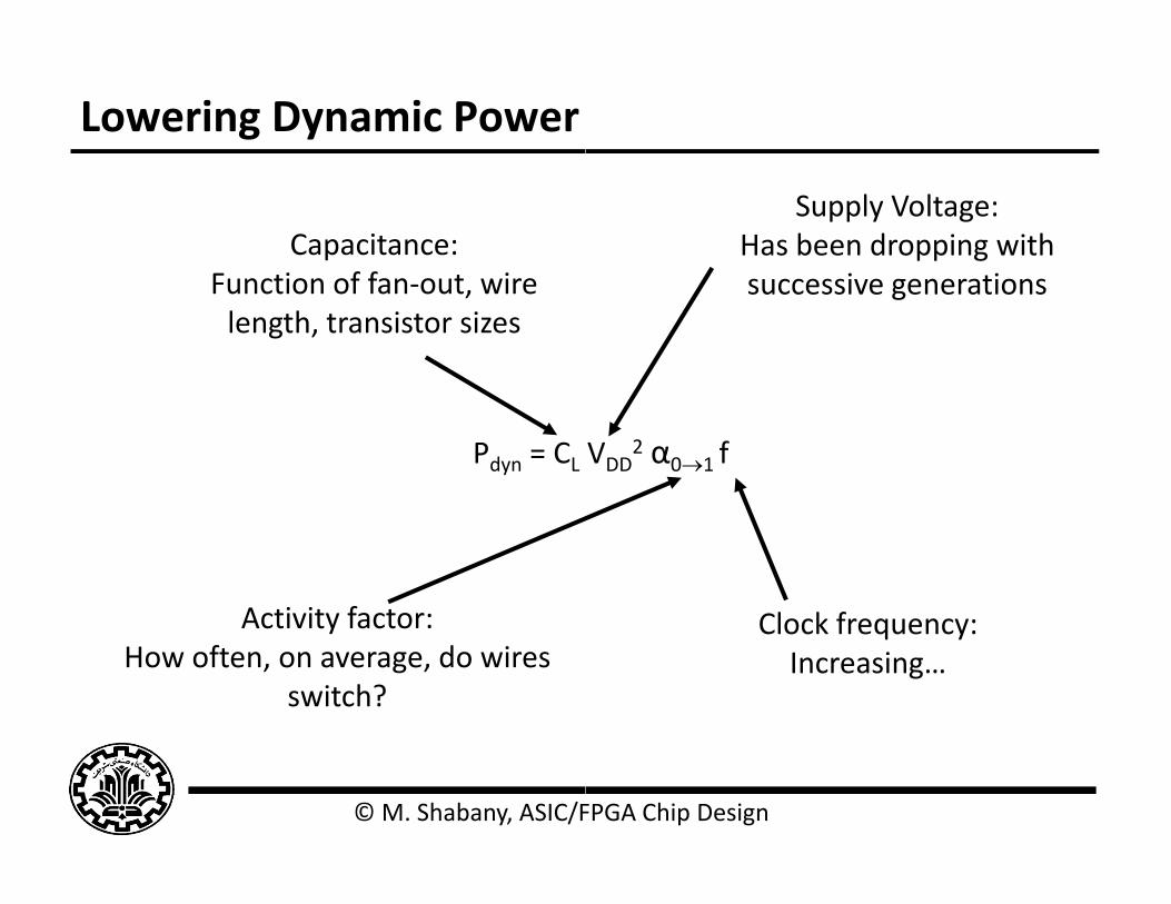
Lowering Dynamic Power
Capacitance:Function of fan out wireFunction of fan‐out, wire length, transistor sizes
Pdyn = CL
Activity factor:Activity factor:How often, on average, do wires
switch?
© M. Shabany, ASIC/F
Supply Voltage:Has been dropping with successive generationssuccessive generations
VDD2 α01 f
Clock frequency:Clock frequency:Increasing…
FPGA Chip Design

Lowering Dynamic Power
Try to minimize:Activity factorCapacitanceSupply voltageFrequency
Pdyn = CLq y
© M. Shabany, ASIC/F
VDD2 α01 f
FPGA Chip Design

Lowering Dynamic Power – Ac
Probability that output is “zero” in ocycle
NN
where
N1
N0
10102
N
2
NPPα
where N0: Number of zero entries in the oN1: Number of one entries in the o
Example: A 2‐input NOR
410 P163
2
3)3(4α
© M. Shabany, ASIC/F
ctivity Factor
one cycle and will be “one” in the next
N )N(2N2N
0N
0
2
)N(2N
output column of the function truth tableutput column of the function truth table
Clk2DDLavg fVC
163
P
FPGA Chip Design
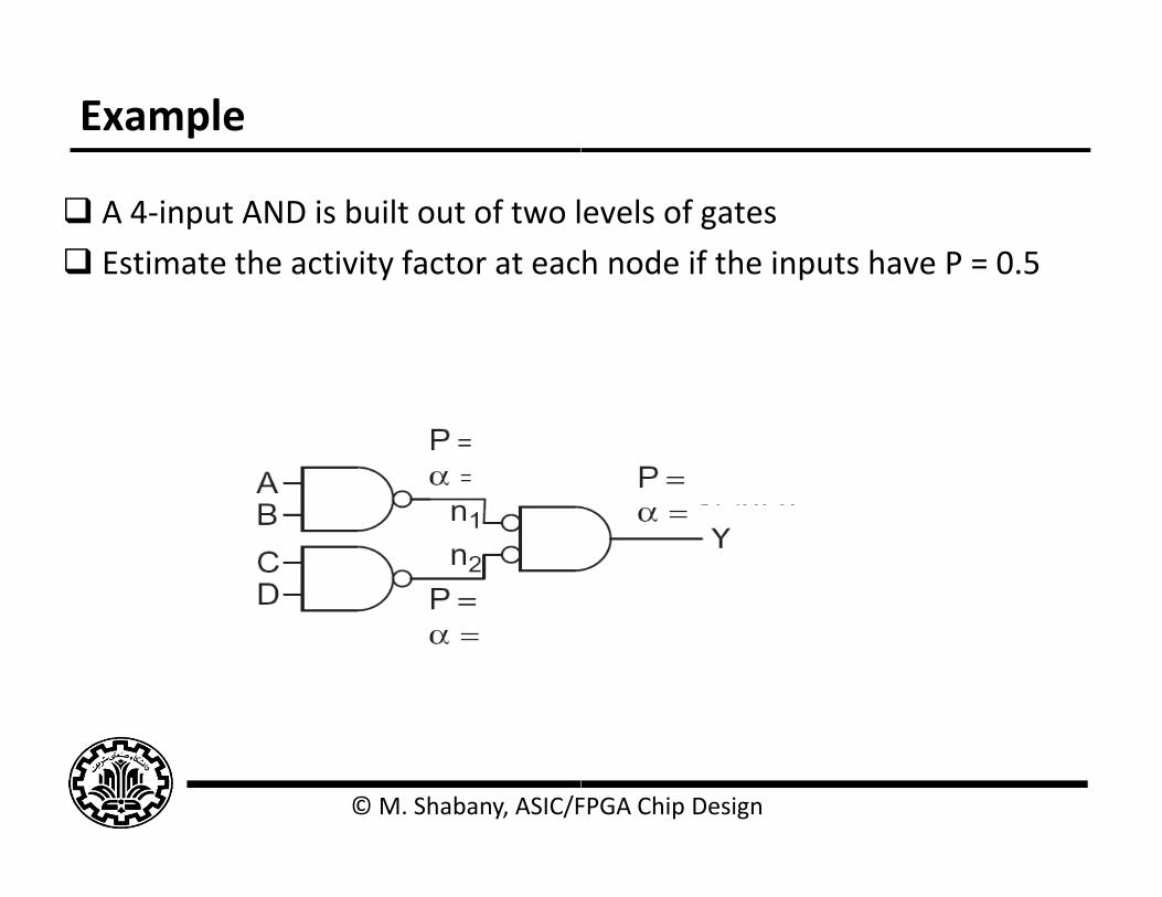
Example
A 4‐input AND is built out of two l
Estimate the activity factor at eacy
© M. Shabany, ASIC/F
evels of gates
h node if the inputs have P = 0.5p
FPGA Chip Design
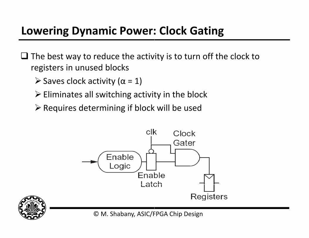
Lowering Dynamic Power:
The best way to reduce the activregisters in unused blocks
Saves clock activity (α = 1)
Eliminates all switching activit
Requires determining if block
© M. Shabany, ASIC/F
: Clock Gating
ity is to turn off the clock to
ty in the block
k will be used
FPGA Chip Design
Lowering Dynamic Power:
Gate capacitance f l Fewer stages of logic
Small gate sizes
Wire capacitanceWire capacitance Good floorplanning to keep com
other
Drive long wires with inverters o
© M. Shabany, ASIC/F
: Capacitance
mmunicating blocks close to each
or buffers rather than complex gates
FPGA Chip Design
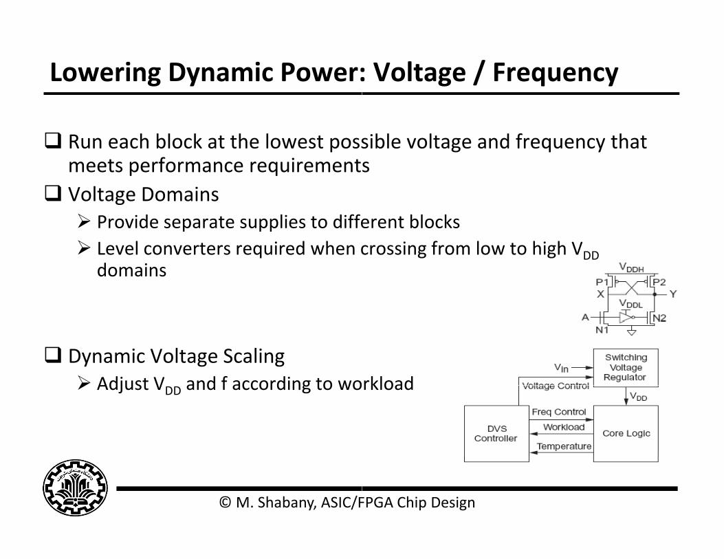
Lowering Dynamic Power:
Run each block at the lowest possmeets performance requirementp q
Voltage Domains Provide separate supplies to diffe L l t i d h Level converters required when c
domains
Dynamic Voltage Scaling Adjust V and f according to wo Adjust VDD and f according to wo
© M. Shabany, ASIC/F
: Voltage / Frequency
sible voltage and frequency that s
erent blocksi f l t hi h Vcrossing from low to high VDD
rkloadrkload
FPGA Chip Design
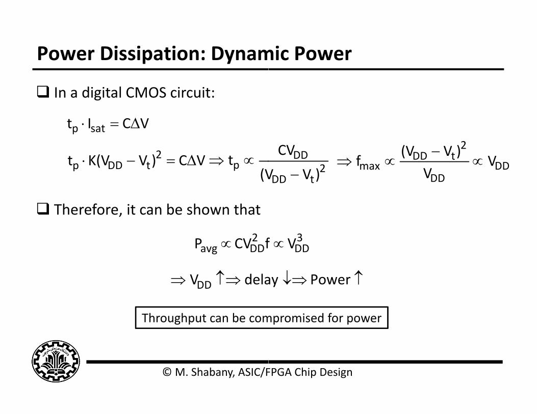
Power Dissipation: Dynam
In a digital CMOS circuit:
VCIt satp satp
VC)VK(Vt 2tDDp p
(Vt
Therefore, it can be shown that
(
2DDavg fCV P
delaVDD
Throughput can be com
DD
© M. Shabany, ASIC/F
mic Power
2tDD
DD
)VV
CV
DDDD
2tDD
max VV
)V(Vf
tDD ) DD
3DDV f
Poweray
mpromised for power
y
FPGA Chip Design
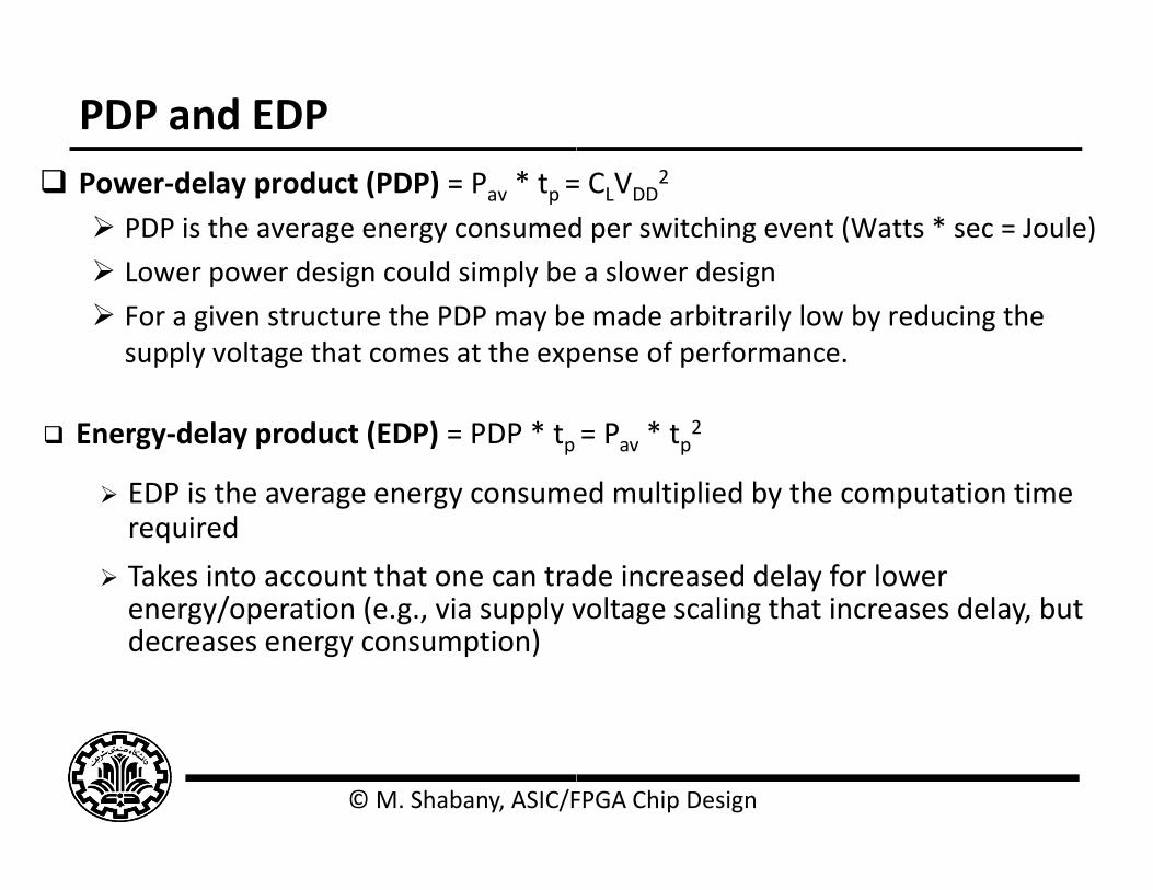
PDP and EDP Power‐delay product (PDP) = Pav * tp = PDP is the average energy consumed
Lower power design could simply be Lower power design could simply be
For a given structure the PDP may besupply voltage that comes at the exp
Energy‐delay product (EDP) = PDP * tp
EDP is the average energy consume EDP is the average energy consumerequired
Takes into account that one can traenergy/operation (e g via supply venergy/operation (e.g., via supply vdecreases energy consumption)
© M. Shabany, ASIC/F
= CLVDD2
d per switching event (Watts * sec = Joule)
a slower design a slower design
e made arbitrarily low by reducing the pense of performance.
= Pav * tp2
ed multiplied by the computation timeed multiplied by the computation time
ade increased delay for lower voltage scaling that increases delay butvoltage scaling that increases delay, but
FPGA Chip Design

PDP and EDP15
aliz
ed)
10
elay
(nor
m
0
5
Ener
gy-D
e
00.5 1
V
Rule‐of‐thumb:
23
VOptDD
© M. Shabany, ASIC/F
2
energy‐delay
energy
delay
1.5 2 2.5
Vdd (V)
2V
VSatDS
t
FPGA Chip Design
2
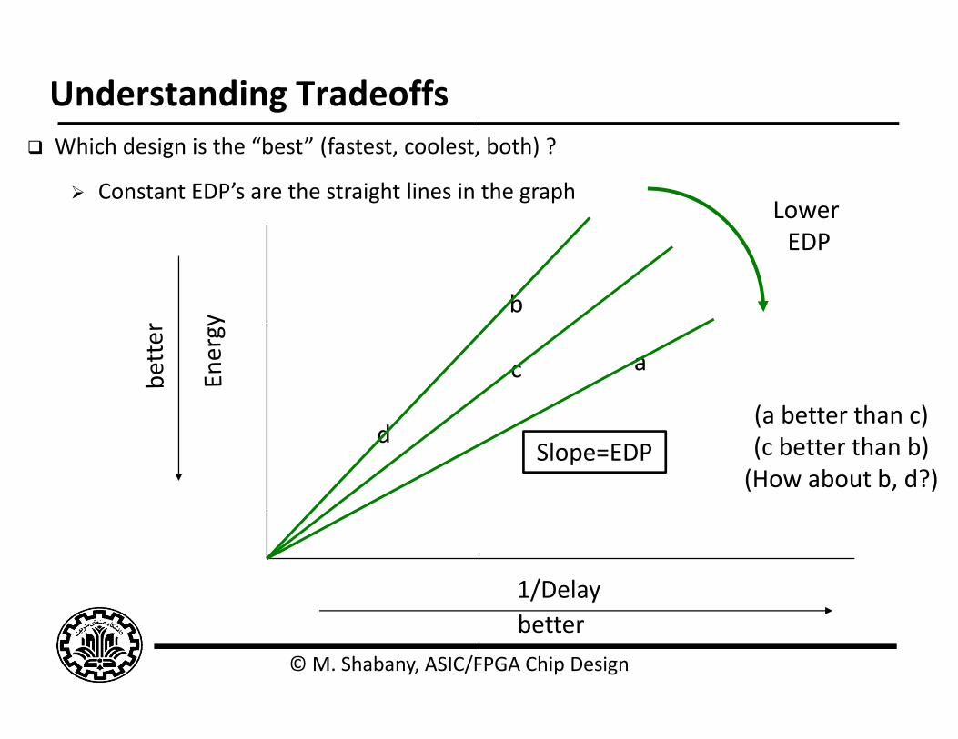
Understanding Tradeoffs Which design is the “best” (fastest, coolest,
Constant EDP’s are the straight lines in
d
© M. Shabany, ASIC/F
Lower
both) ?
the graph
b
EDP
ac
(a better than c)Slope=EDP
(a better than c)(c better than b)(How about b, d?)
1/Delay
FPGA Chip Design
better
Power Dissipation
Power D
Dynamic Power
Short‐circuitMain Dynamic Power Short circuit y
© M. Shabany, ASIC/F
Dissipation
Static Power(L k )
Power
(Leakage)
Power
FPGA Chip Design
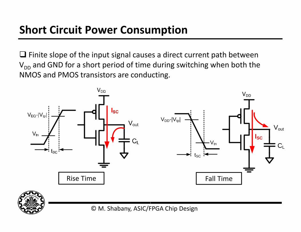
Short Circuit Power Consu
Finite slope of the input signal causeVDD and GND for a short period of timeNMOS d PMOS i dNMOS and PMOS transistors are condu
Rise Time
© M. Shabany, ASIC/F
mption
es a direct current path between during switching when both the iucting.
VDD
Vout
VDD-|Vtp|
CL
ISCVtn
tSC
Fall Time
FPGA Chip Design

Short Circuit Currents Dete
VCItdv
CI
fsc
rscsc ttt
DDscsc,avgsc VCItdt
CI
It sc avgsc
fVItVIP DDDD
T
ItI sc,avgscsc
fVItVIP DDsc,avgscDDscsc
fVCαfVCP 2DDLsc
2DDscsc
2DDLsc
2DDscsc VCαVCE
© M. Shabany, ASIC/F
erminates
Peak and duration of I both increase as thePeak and duration of Isc both increase as the input slope decreases
FPGA Chip Design

Short Circuit Currents Dete
αPsc
sc αE
Ipeak determined by
Saturation current of the P an Saturation current of the P antheir sizes, process technology
Strong function of the ratio beg
Function of CL
© M. Shabany, ASIC/F
erminates
fVC 2DDLsc
2DDLsc VCα
nd N transistors which depend onnd N transistors, which depend on y, temperature, etc.
etween input and output slopesp p p
FPGA Chip Design
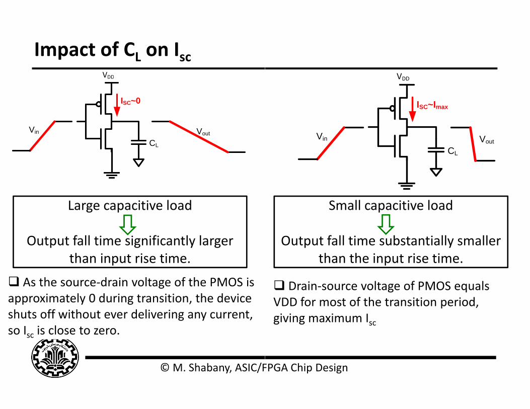
Impact of CL on IscVDDVDD
V
ISC~0
Vout
CL
Vin
Large capacitive load
Output fall time significantly larger than input rise time.
As the source drain voltage of the PMOS is As the source‐drain voltage of the PMOS is approximately 0 during transition, the device shuts off without ever delivering any current, so Isc is close to zero.
© M. Shabany, ASIC/F
so Isc is close to zero.
VVDD
ISC~Imax
Vout
CL
Vin
Small capacitive load
Output fall time substantially smaller than the input rise time.
D i l f PMOS l Drain‐source voltage of PMOS equals VDD for most of the transition period, giving maximum Isc
FPGA Chip Design
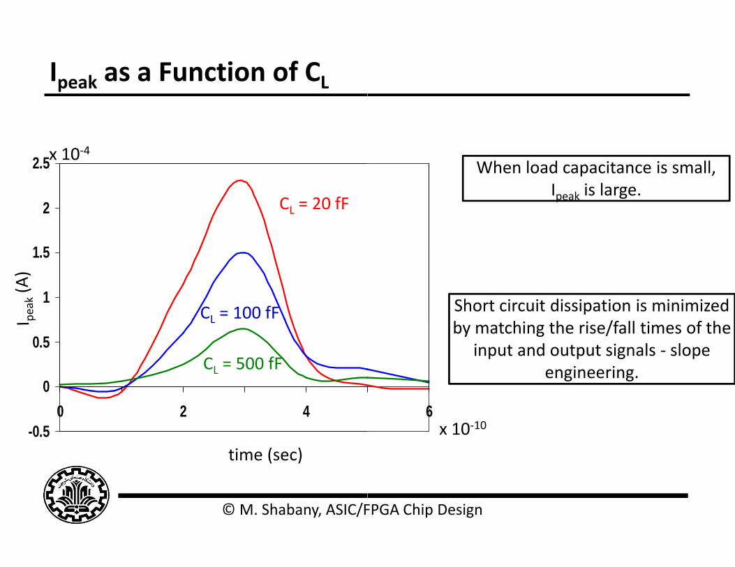
Ipeak as a Function of CL
2.5x 10‐4
1 5
2 CL = 20 fF
1
1.5
CL = 100 fF
0
0.5L
CL = 500 fF
-0.5
00 2 4
time (sec)
© M. Shabany, ASIC/F
( )
When load capacitance is small, pIpeak is large.
Short circuit dissipation is minimized by matching the rise/fall times of the
input and output signals ‐ slope engineering.
6x 10‐10
FPGA Chip Design

Psc as a Function of Rise/Fa8
6
7
8
V = 3 3 V
4
5
6 VDD= 3.3 V
2
3
4
VDD = 2.5 V
0
1
2
VDD = 1.5
00 2 4tsin/tsout
© M. Shabany, ASIC/F
all Times
When load capacitance is small (tsin/tsout > 2 for VDD > 2V) the power is
dominated by Psc
If VDD < VTn + |VTp| then Psc is eliminated since both devices are
never ON at the same timenever ON at the same time.
For large capacitance values, all the power dissipation is devoted to
5V
t e po e d ss pat o s de oted tocharging and discharging the load capacitance. When the rise/fall times of inputs and outputs are equalized, most power dissipation is associated with dynamic power and only a minor
( )
FPGA Chip Design
fraction (<10%) is devoted to Psc.
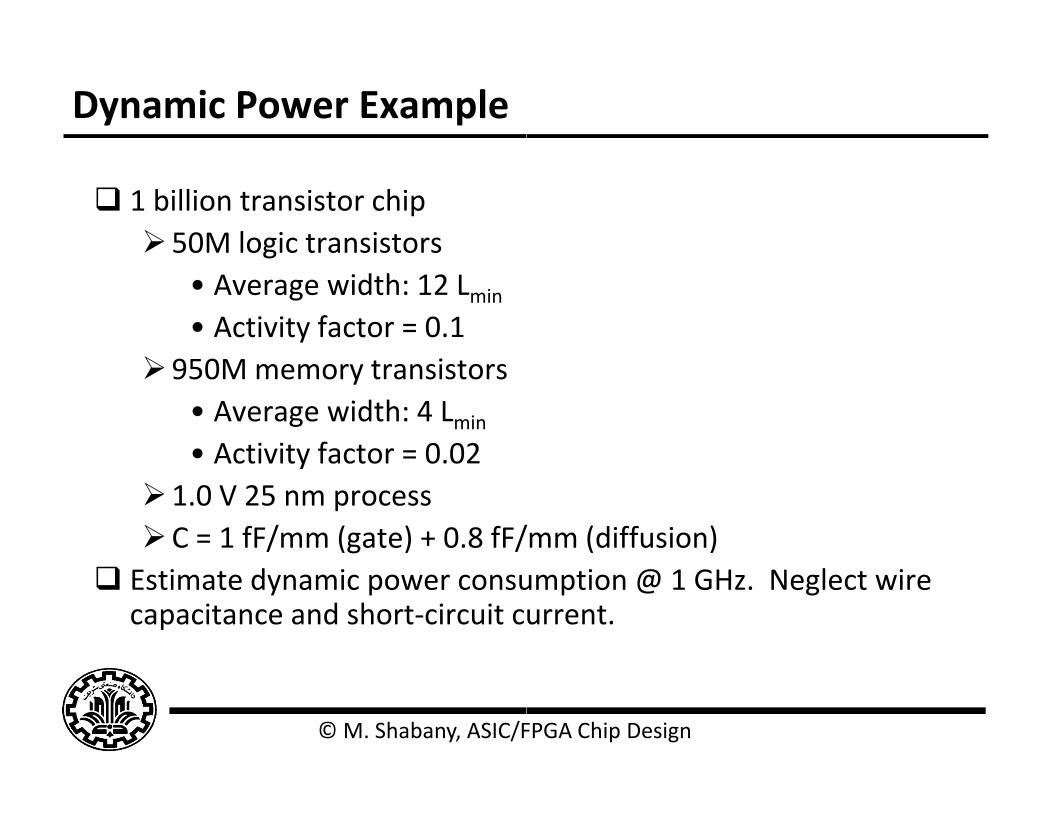
Dynamic Power Example
1 billion transistor chip50M logic transistors50 og c t a s sto s
• Average width: 12 Lmin
• Activity factor = 0.1950M memory transistors
• Average width: 4 Lmin
• Activity factor = 0 02• Activity factor = 0.021.0 V 25 nm processC = 1 fF/mm (gate) + 0.8 fF/
Estimate dynamic power consucapacitance and short‐circuit c
© M. Shabany, ASIC/F
/mm (diffusion)umption @ 1 GHz. Neglect wire urrent.
FPGA Chip Design
Dynamic Power Example
6logic 50 10 12 0.025C m
logic
6mem 950 10 4 0.025
0 1 0 02 1
C m
P C C
dynamic logic mem0.1 0.02 1P C C
© M. Shabany, ASIC/F7: Power
/ 1.8 / 27 nFm fF m
2
/ 1.8 / 171 nF
1 0 1 0 GH 6 1 W
f
m fF m
21.0 1.0 GHz 6.1 W
FPGA Chip Design 39
Outline
• Introductionoduc o
• Dynamic Power Dissipation
• Static Power Dissipationp
© M. Shabany, ASIC/FFPGA Chip Design 40

Power Dissipation
Power D
Dynamic Power
Short‐circuitMain Dynamic Power Short circuit y
© M. Shabany, ASIC/F
Dissipation
Static Power
Power
(Leakage)
Power
FPGA Chip Design
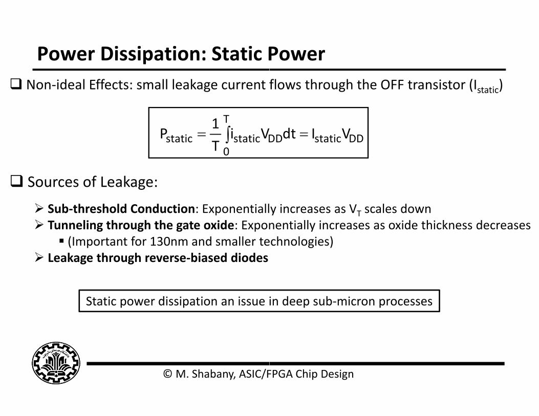
Power Dissipation: Static P Non‐ideal Effects: small leakage current f
TVi
1P
Sources of Leakage:
D0staticstatic Vi
TP
Sources of Leakage:
Sub‐threshold Conduction: Exponentiall Tunneling through the gate oxide: Expon
(Important for 130nm and smaller te Leakage through reverse‐biased diodes
Static power dissipation an issue i
© M. Shabany, ASIC/F
Powerflows through the OFF transistor (Istatic)
VIdt DDstaticDD VIdt
y increases as VT scales downnentially increases as oxide thickness decreasesechnologies)
in deep sub‐micron processes
FPGA Chip Design
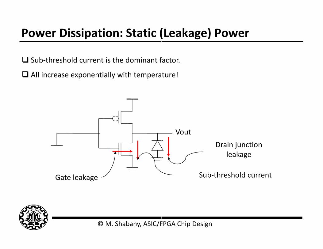
Power Dissipation: Static (
Sub‐threshold current is the dominant f
All increase exponentially with temperap y p
Gate leakage
© M. Shabany, ASIC/F
(Leakage) Power
factor.
ture!
Vout
Drain junction leakage
Sub‐threshold current
FPGA Chip Design
Leakage as a Function of VT
d l f l l d h
10 2
Continued scaling of supply voltage and themake sub‐threshold conduction a dominate
10‐2
ID (A
)
10‐7
VTVT
0 0.2 0.4 0.6 0.8
VGS (V)
10‐12
© M. Shabany, ASIC/F
( )
T
b l f h h ld l lle subsequent scaling of threshold voltage will e component of power dissipation.
An 90mV/decade VT roll‐off ‐ so each 255mV increase in VT giveseach 255mV increase in VT gives
3 orders of magnitude reduction in leakage (but
adversely affects performance)
T=0.4VT=0.1V
1
FPGA Chip Design

TSMC Processes Leakage an
CLCL018 LPCL018 G
42 Å42 ÅTox (effective)
00 160 16L
1.8 V1.8 VVdd
1 6020I (l k )
3500/180600/260IDSat (n/p) (A/m)
00.16 m 0.16 m Lgate
0.63 V0.42 VVTn
1.6020Ioff (leakage) (A/m)
2230FET Perf. (GHz)
(G: generic LP: low power U
© M. Shabany, ASIC/F
(G: generic, LP: low power, U
nd VT
CL013 HSCL015 HSCL018 HSL018 ULP
0 08
24 Å
1.2 V
0 11
29 Å
1.5 V
42 Å42 Å
0 130 18
2 V1.8 V
13 000
920/400
0.08 m
1 800
860/370
0.11 m
3000 15
780/360320/130
0.13 m 0.18 m
0.25 V
13,000
0.29 V
1,800
0.40 V0.73 V
3000.15
80524314
ULP: ultra low power HS: high speed)
FPGA Chip Design
ULP: ultra low power, HS: high speed)
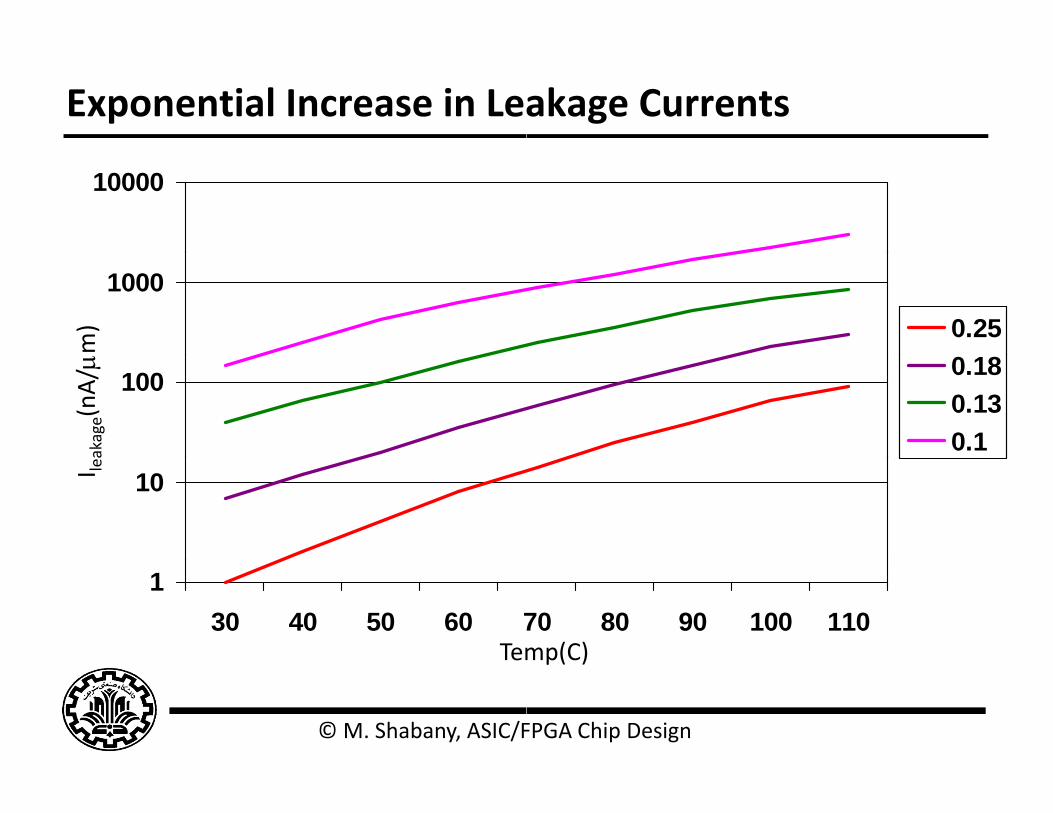
Exponential Increase in Lea
10000
1000
m)
100
akage(nA
/
10I le
130 40 50 60 7
Tem
© M. Shabany, ASIC/F
akage Currents
0.250.180.130.1
70 80 90 100 110mp(C)
FPGA Chip Design
p( )
Leakage Control
Leakage and delay trade offAim for low leakage in sleep a
To reduce leakage: Increase Vt: multiple Vt
• Use low V only in critical c• Use low Vt only in critical c Increase Vs: stack effect
• Input vector control in sleeDecrease Vb
• Reverse body bias in sleepO f d b d bi i• Or forward body bias in ac
© M. Shabany, ASIC/F
and low delay in active mode
circuitscircuits
ep
pti dctive mode
FPGA Chip Design

Gate Leakage
Extremely strong function of tox a
Negligible for older processesg g p
Approaches sub‐threshold leaprocesses
An order of magnitude less for PM
Control leakage in the process us
Hi h k t di l t i h lHigh‐k gate dielectrics help
Some processes provide mult
• e g thicker oxide for 3 3 Ve.g. thicker oxide for 3.3 V
Control leakage in circuits by limi
© M. Shabany, ASIC/F
and Vgs
s
akage at 65 nm and below in some
MOS than NMOS
sing tox > 10.5 Å
iple toxV I/O transistorsV I/O transistors
iting VDD
FPGA Chip Design

Static Power Example
Revisit power estimation for 1 bil
Estimate static power consumpti Estimate static power consumpti Subthreshold leakage
• Normal Vt: 100 nA
• High Vt: 10 nA/
• High Vt used in all memories
Gate leakage 5 nA/m Gate leakage 5 nA/m
Junction leakage negligi
© M. Shabany, ASIC/F
llion transistor chip
onon
A/mm
/mm
and in 95% of logic gates
mmmm
ble
FPGA Chip Design
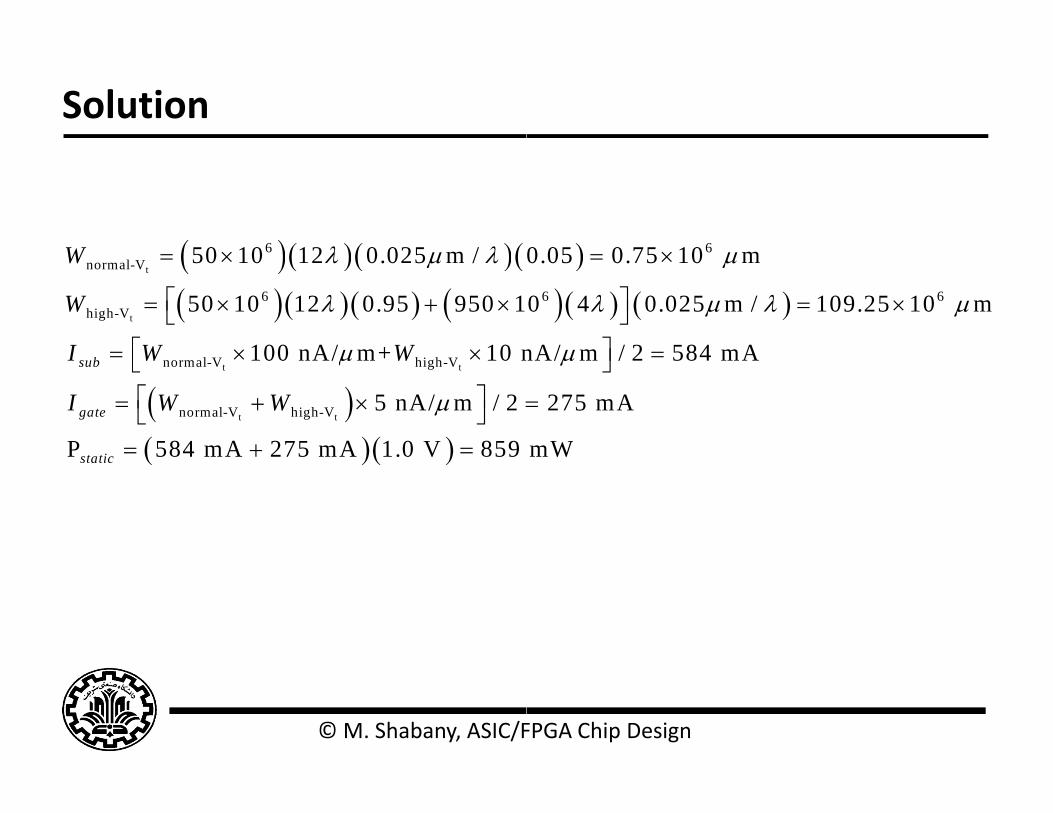
Solution
650 10 12 0 025 m /W
t
t
normal-V
6high-V
50 10 12 0.025 m /
50 10 12 0.95 950 1
100 nA/ m+ 10 n
W
W
I W W
t t
t t
normal-V high-V
normal-V high-V
100 nA/ m+ 10 n
5 nA/ m / 2
sub
gate
I W W
I W W
P 584 mA 275 mA 1.0 V 859static static
© M. Shabany, ASIC/F
60 05 0 75 10 m
6 6
0.05 0.75 10 m
0 4 0.025 m / 109.25 10 m
nA/ m / 2 584 mA
nA/ m / 2 584 mA
275 mA
mW
FPGA Chip Design

Review: Designing Fast CM
Transistor sizing
Progressive transistor sizing
MOS closest to the output is
Transistor ordering
put latest arriving signal closput latest arriving signal clos
Logic structure reordering
replace large fan‐in gates wit replace large fan in gates wit
Apply “logical effort”
Buffer (inverter) insertion
separate large fan‐in from la
uses buffers so there are no
© M. Shabany, ASIC/F
MOS Gates
smallest of series MOS transistors
est to the outputest to the output
th smaller fan‐in gate networkth smaller fan in gate network
rge CL with buffers
more than four TGs in series
FPGA Chip Design