asia nano forum - nanoglobenano-globe.biz/newsletter/anf/anfnewsletterissue12.pdf · nanotechnology...
TRANSCRIPT

Asia Nano Forum NEWSLETTER
(Issue No. 12)
ANF Secretariat, Singapore
January 2011
Editor:
Hongfang JIN
Lerwen LIU
Courtesy of China ANF Summit 2010
Courtesy of Singapore Courtesy of Singapore Courtesy of Vietnam

AASSIIAA NNAANNOO FFOORRUUMM SSOOCCIIEETTYY NNEEWWSSLLEETTTTEERR
ISSUE No.12 January 2011
Copyright © 2007‐2011 Asia Nano Forum (ANF). All Rights Reserved. 2 of 28
Table of Contents
NEWS.....................................................................................................................3
ANF Activities...........................................................................................................................3
Partnerships/Collaborations....................................................................................................6
Commercialization and Business ...........................................................................................14
New education/research program ........................................................................................17
RESEARCH BREAKTHROUGH ..................................................................19
NEW PUBLICATION......................................................................................27
EVENTS.............................................................................................................28

Copyright © 2007‐2011 Asia Nano Forum (ANF). All Rights Reserved. 3 of 28
AASSIIAA NNAANNOO FFOORRUUMM SSOOCCIIEETTYY NNEEWWSSLLEETTTTEERR
ISSUE No.12 January 2011
NEWS
ANF Activities
ANFoS2010
ANFoS2010 was successfully held on the 9 November 2010 at Hanoi University of Science and Technology. This
event was hosted by Vietnam Academy of Science and Technology and co-organized with Asia Nano Forum and
National Institute of Materials Science ( NIMS, Japan).
Bringing together about 40 invited delegates in government funding agencies, research institutes, and industries from
13 Asian economies and 8 observers, this Summit updated on nanotechnology development in each participating
economy, held its Annual General Meeting and set strategic directions for development and regional collaboration in
nanotechnology among the member economies. The updates include past year’s nanotechnology development in the
areas of policy, R&D, education, commercialization, safety and standardization, infrastructure, as well as international
collaboration.
ANF Annual General Meeting
(AGM) was held on the same
day where ANF secretary
working report, Working Group
briefings were conducted. ANF
Secretary, Dr.Lerwen Liu gave a
representation on ANF Financial
Statement and Secretariat
activities in year 2008-2009. Dr.
K.W. LIM submitted the resignation as Vice President and recommend Dr. A. Hor (new Executive Director of
IMRE, Singapore) to be the new Vice President. ANF members thank Dr. K.W. LIM for his three years’ hard work
and great support of ANF activities.

Copyright © 2007‐2011 Asia Nano Forum (ANF). All Rights Reserved. 4 of 28
AASSIIAA NNAANNOO FFOORRUUMM SSOOCCIIEETTYY NNEEWWSSLLEETTTTEERR
ISSUE No.12 January 2011
Dr. Tsung-Tsan SU gave a liaison report on ANF participation in ISO/TC 229 which included a summary of recent
activities, member activities on nano standardization and ANF activities related to ISO/TC 229.
Dr. Ramam AKKIPEDDI briefed on the Asia Nanotech Camp 2010 (ANC2010). The Camp included lectures and lab
visits, demonstrations, group competitions, social activities and poster session. He also shared helpful suggestions
presented by the ANC participants for improving future ANC.
Dr. T. TURNEY represents Australia provided overview on Australia Nanosafe network and recommendation for
ANF EHS collaborative program, and Dr Ali BEITOLLAHI presented overview on Iran EHS efforts. All ANF
members agreed on the initiation of ANF EHS collaboration/joint research program/projects.
Some proposals were come up: 1). Set up Nano EHS Database – List all the well characterized nanomaterials on one
website and identify nano toxicity experts from each economy; Collect information on what’s going on elsewhere. 2).
Organized a kick off Nano EHS workshop around mid 2011 in Singapore. 3). It was suggested to follow the Australia
Nanosafe network model to organize each economy’s Nano EHS network and converge to ANF network. 4). ANF
could help facilitating the harmonization between regulatory bodies and research communities.
It was approved by members that Korea will host Asia Nano Camp 2011. Both Korea and Iran proposed to host
ANFoS2011. After voting, Iran won Korea by 6:5 and will be the host of ANF summit 2011. The date is yet to be
announced, but it will be in Oct. 2011 in Tehran.
ANC 2010 - The brightest young minds in nanotechnology from across Asia gather in Singapore to talk shop and
shop?
Starting on October 4th 2010, the next generation of nanotechnology scientists from 35 universities in 13 countries and
territories across the Asia-Pacific region (including Australia, China, India, Indonesia, Iran, Japan, Korea, Malaysia,
New Zealand, Singapore, Taiwan, Thailand, and Vietnam) met in Singapore and Malaysia over a period of 12 days.
Participants of the camp not only discussed and formed collaborations on nanotechnology, but also experienced the
cultures of their host nations.
Participants presented their
research on nanostructured
materials and devices, as
well as discussed the impact
of nanoscience and
nanotechnology on society.
A substantial part of the
programme also involved
participants in activities to discover more about their host nations, research-wise, economically and culturally.

AASSIIAA NNAANNOO FFOORRUUMM SSOOCCIIEETTYY NNEEWWSSLLEETTTTEERR
ISSUE No.12 January 2011
Copyright © 2007‐2011 Asia Nano Forum (ANF). All Rights Reserved. 5 of 28
The participants visited Singapore universities, research organisations and local companies which employ
nanotechnology research such as Hyflux. They also participate d in a cultural immersion programme which will
introduce them to the sights, sounds, diversity, and tastes of Singapore.
"Just as important as the discussions and exchange of ideas on research are, the camp is unique as it is designed to
allow the participants to learn more about R&D, the economy and the way people live in the host countries", explained
Prof Andy Hor, Executive Director of A*STAR's IMRE, whose nanotechnology R&D examples include
nanostructured materials, nanocomposites, nanopatterning and nanoimprinting. IMRE is one of the hosts of this year's
camp and where ANF is headquartered.
Echoing his sentiments, Dr Lim Khiang Wee, Vice-President of ANF said, "The camp is a networking opportunity for
these young researchers. This 'peer support group' will be essential to them in the future when they begin take on their
roles as principal drivers of research and innovation in their respective countries".
The camp hosted young talented researchers like Dr Davy Cheong from Singapore who is looking to commercialise
his new cornstarch-inspired, flexible, lightweight, impact-resistant composite material made for body armour and
protective sports padding, and Dr Ratno Nuryadi from Indonesia who built a fully-functional nanoscope from
commonly available parts at less than a tenth of SGD400,000 price tag of commercial systems.
"Davy and Ratno are examples of the calibre of the young researchers who are attending the camp. They represent the
new ideas, unconventional thinking and can do spirit that we hope this networking will create. Who knows? We could
very well have a future Nobel Laureate in our midst!" added Prof Andy Hor.
The annual camp was initiated in Japan two years ago by the Asia Nano Forum (ANF) network, an organisation
spanning 15 countries in the Asia-Pacific region, which was founded in 2004 to promote excellence in research,
development and the economic uptake of nanotechnology within the Asian region. This is the first time the camp is
co-hosted by two nations, Singapore and Malaysia.

Copyright © 2007‐2011 Asia Nano Forum (ANF). All Rights Reserved. 6 of 28
AASSIIAA NNAANNOO FFOORRUUMM SSOOCCIIEETTYY NNEEWWSSLLEETTTTEERR
ISSUE No.12 January 2011
Partnerships/Collaborations
China
The First CHINANO Forum & Exhibition Themed at Nanotech Application and Industrialization Are Held at Suzhou,
China ( NanoGlobe)
China is one of the pioneer countries worldwide developing
nanotechnology and had invested 1.2 billion RMB (around 1800 million
USD) on nanotechnology during the 10th Five Year Plan. In the 11th Five
Year Plan, the investment on nanotechnology has been budgeted over 2
billion RMB (around 3000 million USD). Nanotechnology, as one of the
most powerful emerging high-technology, is expected to have a
revolutionary impact on life science, new materials, energy, environment,
electronics, automotives, aerospace and safety. It is believed to benefit citizens and improve industrial competitiveness
within twenty years or beyond. In China, the number of national projects on nanotechnology R&D is increased from
100 to 965 in the past 10 years. Nevertheless, there is a lot of work for China to do in the nanotechnology R&D and
industrialization before China can catch up with those leading countries such as US, Germany, Japan and Korea. The
first CHINANO Forum & Exhibition held in November 13-15th 2010 at Suzhou International Expo Center, focusing
on nanotechnology application and industrialization, is aimed to serve as a sustainable platform bringing together
worldwide R&D and industry leaders to share the latest advancement in nanotechnology R&D and commercialization,
as well as business opportunities enabled by nanotechnology.
CHINANO Forum 2010 is organized by Ministry of Science and
Technology of China, Chinese Academy of Sciences and Jiangsu Provincial
People's Government, and hosted by Jiangsu Science and Technology
Department and Suzhou Municipal People's Government. In the morning of
the first day, Dr Kazumi matsushige from Kyoto University (Japan), Mr
Grudev Vasiliy from RUSNANO (Russia), Dr Péter Krüger from Bayer
Materials science (Germany) and Dr Markku Lämsä from Tekes, Finland
were invited to give plenary presentation on academia/industry/government collaboration in nanotechnology R&D and
commercialization in Kyoto and Japan, industrialization of nanotechnology in Russia, chance and challenges of
sustainable commercialization of nanotechnology along the value chain, as well as role of novel materials and
nanotechnology in industry innovation in Finland. In the following one and half days, over 100 keynote presentations
covered five technical sessions: optoelectronic, micro- and nano-manufacturing, nano-medicine and safety, advanced
materials, as well as energy and environment.
In addition, NanoGlobe Pte Ltd (Singapore), as a co-organizer of CHINANO Forum 2010, organized the most popular
session in this forum - Nanotechnology Investment: Opportunities and Challenges. Dr Lerwen Liu, managing director

AASSIIAA NNAANNOO FFOORRUUMM SSOOCCIIEETTYY NNEEWWSSLLEETTTTEERR
ISSUE No.12 January 2011
Copyright © 2007‐2011 Asia Nano Forum (ANF). All Rights Reserved. 7 of 28
of NanoGlobe chaired this session bringing together world leading government and private investors in
nanotechnology such as Mr Jim Von Ehr, President & Founder of Zyvex Corporation (USA), Mr. Jianjiang Fei,
Executive Vice President of Suzhou Ventures Group, Mr. Russell L. Boltwood, Executive Vice President & General
Counsel of Transpacific IP (Singapore), and Dr Gerd Bachmann, Nanotechnology Expert Consultant to the Federal
Ministry of Education and Research (Germany) to share their experience in nanotechnology investment and exit
strategy and to address issues that are relevant to the success of nanotechnology enabled business. During the panel
discussion, attendants had a lively discussion with speakers in terms of the status of nanotechnology
commercialization in China, IP protection and management, attracting professionals, team building and management
especially in China and so on.
The success of CHINANO Forum 2010 is a well begun. Suzhou, as one of the leading modern and innovative cities in
China, is promoting the adoption of nanotechnology in industries and welcomes the worldwide research institutes and
industries to collaborate with Suzhou research institution and industries and setup their R&D centers or manufacturing
facilities in Suzhou Industrial Park (SIP). Headed by SIP, 10 billion RMB (around 1.5 billion USD) will be invested
within 5 years to build a new nanotech R&D and industrialization hub in Suzhou.
China's Bionanotechnology Company Suzhou Natong Wins the Silver Prize of the Asian Innovation Awards 2010
( Suzhou Natong Bionanotechnology)
Suzhou Natong with its US partner Nanomed Devices, Inc. announced on November 3rd 2010 that they won the Silver
Prize of the Asian Innovation Awards 2010 at the Biobay Investor Forum. The award was sponsored by The Wall
Street Journal Asia in partnership with Credit Suisse AG.
Suzhou Natong Bionanotechnology received the Silver Award for creating a drug-delivery device that uses a set of
needles smaller than human hairs for painless injections.
This year the Asian Innovation Awards attracted nearly 300 entries from 13 countries and territories throughout Asia
Pacific. They were judged on their ability to enrich and improve the quality of life and productivity across the region.
Speaking at the gala event, Marcel Kreis, head of private banking, Asia Pacific at Credit Suisse, said, "I would like to
congratulate this year's winners for their remarkable effort in coming up with an innovative idea and turning it into a
reality that helps enrich and improve the quality of life and productivity among communities in Asia Pacific and
around the world. We will continue to support the Asian Innovation Awards in the hope of creating inspiration to
others in making this world a better place to live in, working for the common good and bringing about lasting change."
"The need to innovate is a crucial part of good business practice. The ability to develop creative ideas and see new
opportunities to fruition brings companies renewed growth and investment for the future," said Almar Latour, The
Wall Street Journal's editor in chief in Asia. "We received a record number of very high-caliber entries in this year's
awards and we're proud to have provided a platform to showcase their creative ideas and innovative concepts."

AASSIIAA NNAANNOO FFOORRUUMM SSOOCCIIEETTYY NNEEWWSSLLEETTTTEERR
ISSUE No.12 January 2011
Copyright © 2007‐2011 Asia Nano Forum (ANF). All Rights Reserved. 8 of 28
Dr. Bai Xu, CEO of Suzhou Natong Bionanotechnology, said at the ceremony, "Winning the prize is the recognition of
our company's innovation and potentials. It will help us to build up the reputation and good image of the company and
is significant to our future."
Iran,
Venezuela Ink MoU on Development of Nanotechnology (INIC)
TEHRAN (INIC) - Iran Nanotechnology Initiative Council (INIC) and the Venezuelan Science Ministry's Center for
Science and Technology Researches signed a Memorandum of Understanding (MoU) on interacademic cooperation in
the field of nanotechnology. Based on the MoU, the aforementioned organizations will cooperate in exchanging
students and conducting research projects in the field of nanotechnology. A Venezuelan delegation, comprising
Guillermo Barrerto, CEO of Science and Technology Center at Venezuelan Ministry of Science, and Roben Machado,
head of Iowik Research Center (a Venezuelan Ministry of Science affiliate) and other ranking officials, visited the
third Iran Nanotechnology Festival (October 25 to 29), where they were briefed about Iran's achievements in the field
of nanotechnology. "We traveled to Iran to visit this festival and sign MoUs of cooperation within the scope of
nanotechnology study affairs because Venezuela is at the preliminary stages in nanotechnology and the researches of
Iranian experts could be useful in helping Venezuela to develop nanotechnology", Barrerto said.
Japan
New Nano Ventures in Japan ( NanoGlobe)
NanoGlobe is always looking closely at nano-related business and research in Japan as they have leading edge
technologies as well as application expertise. NanoGlobe works with such companies and can help you do business
and expand partnerships in Japan. On Nov. 10th, 2010 a Nano Biz-Match event was held in Tokyo, sponsored by the
Nanotechnology Business Creation Initiative (NBCI) and the Japanese trade organization JETRO. 7 interesting
businesses and technologies were presented:
1) Advanced Soft Materials Inc.(ASMI)
Slide Ring Material that is like a necklace at the molecular level, with chains of poly ethylene glycol, and on the chains
are sliding rings of cycledextrin. See animations here. The sliding rings give the materials dramatic elongation
properties. First use has been as a durable coating on NEC's mobile phones in Japan. They are also working with car
companies for durable coatings. Due to the expansion properties, actuators have also be created using them. Other
possible applications are for shock absorbing materials, adhesives, contact lenses etc.
2) MTechnique
A thin film micro reactor based on a totally new approach is very impressive. The throughput is scalable and provides
surprising good controllability of reaction and nano-particle size. Basically a reactor where 2 material are introduced
into the micro reactor, and a reaction A+B produces a compound X that is ejected as a thin film which can be used to
create new nano-particles for new materials, new medicines (eg. soluble medicines), bio materials etc.

AASSIIAA NNAANNOO FFOORRUUMM SSOOCCIIEETTYY NNEEWWSSLLEETTTTEERR
ISSUE No.12 January 2011
Copyright © 2007‐2011 Asia Nano Forum (ANF). All Rights Reserved. 9 of 28
Using a circular flow (shown here), they can control where the reaction occurs, the ratios of A and B, size of
nano-particles, speed of reaction, and gives a sharp distribution of particle size, and gives particles of spherical shape.
Instead of the trend of using more and more energy to get smaller and smaller materials, they have introduced a new
bottom-up approach to produce small particles that uses little energy.
3) ISMAN J
They are creating silicon based alloys that are twice as hard as steel but 40% lighter. So far being used for ball
bearings in wind turbines. Other uses likely in automotive etc. where lightness and durability are demanded. A silicon
and nitrogen gas is cooled to give a unique crystal structure (also contains some aluminium) and then turned into a
powder which can be molded into various forms.
4) Bayer Materials Science
Bayer's carbon nanotubes called "Baytubes". Have 3-15 walls (inner diameter~4nm; outer diameter~16nm) which
produced in high quality and at volumes of 260 tons per year. Being used in hockey sticks, skis etc. for its flexibility
and durability. Possibilities for automotive uses.
5) Nagoya University, Graduate School of Engineering, Associate Professor, Koshi Takenaka
They have developed Manganese Nitride(Mn3XN) based materials with negative thermal expansion coefficients, such
that the materials contract with temperature, rather than the usual expansion. The negative expansion can be used
directly to create temperature dependent materials.
Or it can be combined with other materials so that thermal expansion is zero. Such zero expansion materials can be
used for precision instruments that cannot tolerate temperature expansion such as, semiconductor equipment, optical
equipment, precision components etc. And is cheaper than Titanium.
6) SIJ Technology
They have created 'Super Ink Jet' machines that 'print' materials at the micron level, with droplets with micron-level
size and droplet volumes at the femto-litre level. It is fast drying, and can provide an on-demand patterning of
materials. Has been used to print organic transistors. Also useful to pattern digi-gate electrodes, micro bumps, protein
patterning. Future uses includes LEDs, printed electronics, solar cells etc.
7) YOUTEC
They produce CVD, sputtering, annealing equipment as well as working on materials like diamond-like carbon (DLC).
They actually have a high market share in DLC actuators in hard-disk drive heads, and DLC film use in also moving to
the discs themselves.
If you wish to inquire about, or pursue partnerships, with such companies in Japan, please contact NanoGlobe.
Korea
Copyright © 2007‐2011 Asia Nano Forum (ANF). All Rights Reserved. 10 of 28
AASSIIAA NNAANNOO FFOORRUUMM SSOOCCIIEETTYY NNEEWWSSLLEETTTTEERR
ISSUE No.12 January 2011
Korea Inter-agency Meeting on Nano-safety (KISTI)
Cooperative action plans on the safety issues of nanomaterials are being made between the government parties
concerned. Ministry of Education, Science and Technology (MEST), Ministry of Knowledge Economy (MKE),
Ministry of Environment (ME) and Korean Food and Drug Administration (KFDA) held jointly “Nano-safety Policy
Council” on October 19, 2010 and agreed on reinforcing the interagency cooperation for the safety management of
nanomaterials in the future.
It was also decided for the Ministry of Employment and Labor to take part in the Nano-safety Policy Council and
accordingly, cooperative correspondence among the government departments toward the safety problems is expected
to be expedited and handled more efficiently.
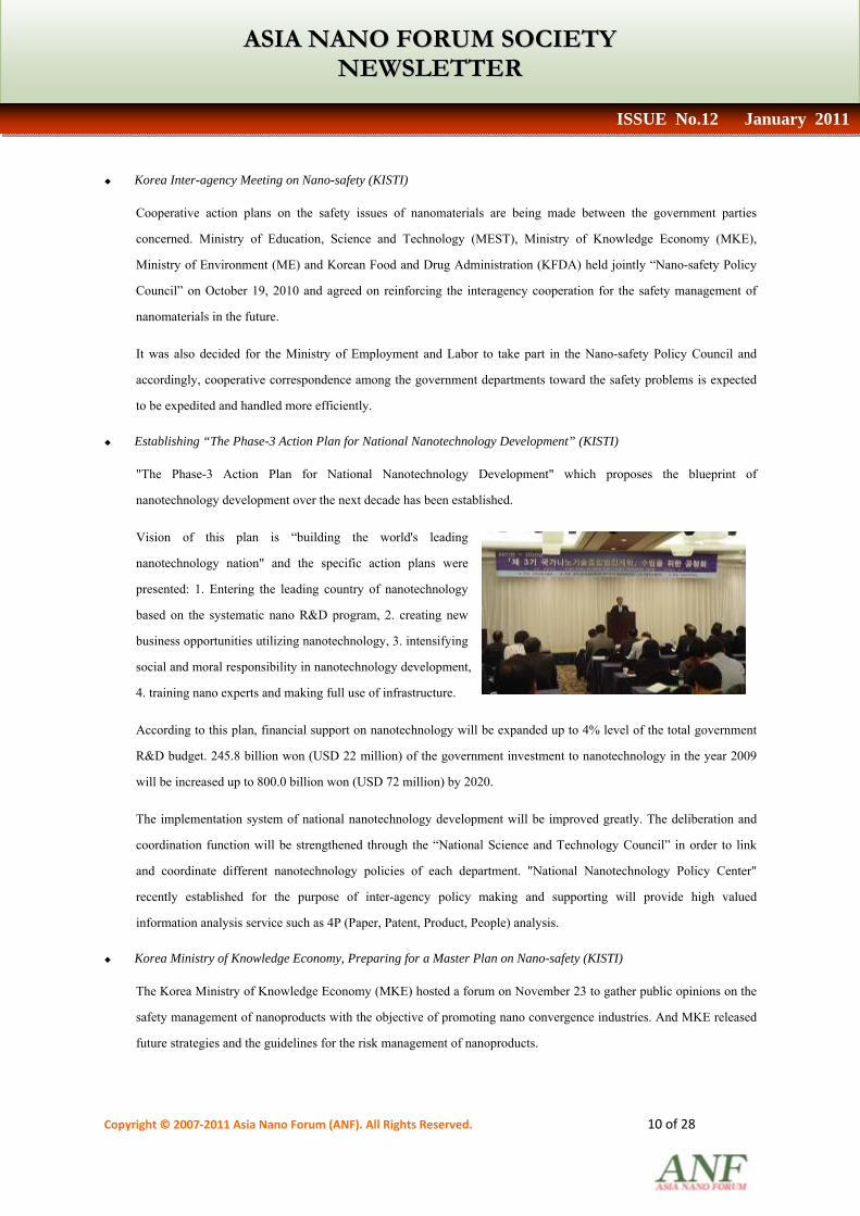
Establishing “The Phase-3 Action Plan for National Nanotechnology Development” (KISTI)
"The Phase-3 Action Plan for National Nanotechnology Development" which proposes the blueprint of
nanotechnology development over the next decade has been established.
Vision of this plan is “building the world's leading
nanotechnology nation" and the specific action plans were
presented: 1. Entering the leading country of nanotechnology
based on the systematic nano R&D program, 2. creating new
business opportunities utilizing nanotechnology, 3. intensifying
social and moral responsibility in nanotechnology development,
4. training nano experts and making full use of infrastructure.
According to this plan, financial support on nanotechnology will be expanded up to 4% level of the total government
R&D budget. 245.8 billion won (USD 22 million) of the government investment to nanotechnology in the year 2009
will be increased up to 800.0 billion won (USD 72 million) by 2020.
The implementation system of national nanotechnology development will be improved greatly. The deliberation and
coordination function will be strengthened through the “National Science and Technology Council” in order to link
and coordinate different nanotechnology policies of each department. "National Nanotechnology Policy Center"
recently established for the purpose of inter-agency policy making and supporting will provide high valued
information analysis service such as 4P (Paper, Patent, Product, People) analysis.
Korea Ministry of Knowledge Economy, Preparing for a Master Plan on Nano-safety (KISTI)
The Korea Ministry of Knowledge Economy (MKE) hosted a forum on November 23 to gather public opinions on the
safety management of nanoproducts with the objective of promoting nano convergence industries. And MKE released
future strategies and the guidelines for the risk management of nanoproducts.

AASSIIAA NNAANNOO FFOORRUUMM SSOOCCIIEETTYY NNEEWWSSLLEETTTTEERR
ISSUE No.12 January 2011
Copyright © 2007‐2011 Asia Nano Forum (ANF). All Rights Reserved. 11 of 28
The master plan will consist of 3 phases over the period of year 2011 through 2020, phase 1(2011~2013), phase
2(2014~2017) and phase 3(2018~2020) and 5 implementation strategies will be set forward: 1. life cycle management
of nanoproducts, 2. R&D on safety evaluation and measurement, 3. establishment of safety certification system in
consumer workplace, 4. revitalization of the nanoproducts market, 5. implementation of proper legislation and
international cooperation.
This project will be pushed forward in three phases to build the infrastructure of life cycle management of
nanoproducts from production to distribution stages:
① Phase 1(2011~2013) - List of nanoproducts will be prepared. Investigation of the products using 13 representative
manufactured nanomaterials selected by the OECD WPMN (Working Party for Manufactured Nanomaterials) will
start soon.
② Phase 2(2014~2017) - It will be mandatory for the manufacturers and importers of nanoproducts to register their
products.
③ Phase 3(2018~2020) - The Product Certification System based upon the Quality Management and Safety Control
of Industrial Products Act will be introduced.
Taiwan
Annual Inspection of Core Facilities for Nanoscience and Nanotechnology (Sinica)
The Office of National Program on Nanotechnology in Taiwan is setting about a series of annual inspection activities
separately in northern, southern and eastern Taiwan during Jan 5th, 6th, 13th, 18th and 20th in 2011. The inspection
crew is now on the visiting schedule from Tsing Hua University (NTHU), National Chiao Tung University, National
Synchrotron Radiation Research Center (NSRRC), National Cheng Kung University (NCKU), National Sun Yat-Sen
University (NSYU),National Dow Hwa University (NDHU), Tzu Chi University and National Taiwan University
(NTU) to carry out a regular check-up for the examination of the nano core facilities setting up in different institutes in
Taiwan.
Thailand
The 3rd SEA-EU-NET Conference: Sharing the Benefits of Joint Research
The Third Bi-Regional EU-SEA S&T Stakeholders’ Conference, the so called Budapest Conference with the
overriding theme of “Sharing the Benefits of Joint Research” was held from November 24-25, 2010 in the prestigious
Buda castle area in Budapest, Hungary.
Prof. Sirirurg Songsivilai, Executive Director of NANOTEC attended the Steering Committee meeting as a
participating member. The Steering Committee oversees the development and implementation of the SEA-EU-NET
program. In recent years the increase in FP7 research projects involving Southeast Asia partners are on the rise. For
Thailand, the number of projects and the amount of funds for Thailand in FP7 is already equal to those in the entire 5
years of FP6. The success rate of Thai proposals is also doubled – from 13.7% to 27% – higher than the overall

Copyright © 2007‐2011 Asia Nano Forum (ANF). All Rights Reserved. 12 of 28
AASSIIAA NNAANNOO FFOORRUUMM SSOOCCIIEETTYY NNEEWWSSLLEETTTTEERR
ISSUE No.12 January 2011
success rate of 19.6%. This is certainly a very encouraging sign for Thailand and helps to promote global visibility for
the nation.
At the conference, Prof. Songsivilai was invited to give a Remark at the
Opening Ceremony of the Conference, together with Prof Andrew Sors
(Rector of Collegium Budapest) and Dr Robert Burmanjer (Head of Unit,
DG Research of the European Commission). He also gave a presentation on
“Biomedical Research in Thailand” and participated in a TV interview
program on the strength of S&T in Thailand and the opportunity for
collaboration between Europe and Southeast Asia.
The primary objective of the conference is to bring scientific experts and policymakers together from Europe and
South East Asia to facilitate exchange of views on the outcomes and benefits of research activities both in EU and
SEA regions. Thematic workshops, presentations, a poster session and several roundtable discussions are planned for
participants with various scientific and institutional backgrounds to serve this goal.
NANOTEC (Thailand) joins force to help flood victims in Thailand (NANOTEC)
The flood situation in Thailand has certainly shown to the world
that we Thais can work as a team and we can pull through this
together. Various sectors of the society are doing their part to help
flood victim get through this nightmare safe and sound.
NANOTEC for its part is also supporting the humanitarian effort.
On October 27, 2010 NANOTEC joined H.E. Dr. Virachai
Virameteekul, Minister of Science and Technology in presenting
Nano Bednets to flood victims at the Royal Thai Army Headquarter. In addition to Nano bednets, NANOTEC has also
presented herbal extract mosquito repellent spray to flood victims.
Launched: Nanotechnology Association of Thailand (NANOTEC)
On October 7, 2010 The Nanotechnology
Association of Thailand was officially launch
by Prof. Songsivilai, President of the
Association, at Queen Sirikit National
Convention Center, Bangkok, Thailand. The
launch program included a special talk by Mr.
Payungsak Chartsutipol, Chairman of The
Federation of Thai Industries on “Capability of Thai industries: Innovation and Technology Challenges”. Prof.
Songsivilai also gave a talk on “The role of the Association towards society and economy”.

Copyright © 2007‐2011 Asia Nano Forum (ANF). All Rights Reserved. 13 of 28
AASSIIAA NNAANNOO FFOORRUUMM SSOOCCIIEETTYY NNEEWWSSLLEETTTTEERR
ISSUE No.12 January 2011
To add color and excitement to the event, the organizer incorporated a fashion show entitled “Nanotechnology Beyond
Thai Fashion”. “The aim of the association is to work closely with industries, researchers, and policy makers. In 2011,
the Association will launch the NanoQ label which will be Thailand’s answer to building consumers’ confident and set
industrial standards for nanotechnology related products. The success of the association is determined by the keen
participation of its members” said Prof. Songsivilai.
NanoThailand 2010: Nanotechnology for a Sustainable World (NANOTEC)
Nanotechnology Association of Thailand in collaboration with NANOTEC
organized “NanoThailand 2010: Nanotechnology for a Sustainable World” a
premier international conference and exhibition. The event was hold during
November 18-20th, 2010 at Thailand Science Park Convention Center,
Pathumthani, Thailand.
The conception of the NanoThailand 2010 is for it to be a premier international
conference and a series of exhibitions in Nanotechnology, bringing together world-leading researchers, Thai scientists,
entrepreneurs, business partners and exhibitors, in several focused areas of the sciences and technology at the
nanoscale. It is aimed as a platform disseminate to researchers and scientists the latest research results, allow
cross-disciplinary exchange of knowledge to further advance both technological areas and to showcase their latest
inventions and innovations. In the foreseeable, not too distant future, Nanotechnology will significantly impact various
large industries and SMEs domestically, regionally and beyond.
IWAMSN2010 (NANOTEC)
International Workshop on Advanced Materials Science and Nanotechnology (IWAMSN2010) was held in Hanoi on
Nov. 9-12, 2010. The conference was organized jointly by Vietnam Physical Society, Vietnam Academy of Science
and Technology and 3 top Universities of Vietnam. About 140 international participants and 160 domestic scientists
attended the event. This was for the first time a scientific conference on nanotechnology attracted an official
participation of the National Council on Science and Technology Policy of Vietnam - an advisory body to the country
Premier.

AASSIIAA NNAANNOO FFOORRUUMM SSOOCCIIEETTYY NNEEWWSSLLEETTTTEERR
ISSUE No.12 January 2011
Copyright © 2007‐2011 Asia Nano Forum (ANF). All Rights Reserved. 14 of 28
Commercialization and Business
Iran
Sharif University of Technology Makes $1.4mln from Nano Products (INIC)
TEHRAN (INIC) - Sharif University of Technology, Iran, managed to gain $1.4mln by offering nanotech-related
services, including cooperating in projects and supporting different researches, ideas and projects. The University has
so far tried to maintain a healthy job market to employ human resources specialized in the fields thereof. Until now,
some of these activities have led to patent applications. ”Sharif University of Technology has gained more than
$1.4mln .On the other hand, the Roshd Center has managed to publish 8 national and 16 international scientific papers
as well as two books, so far. To speak of the employing activities, I am glad to say that many job applicants including
4 Phd, 10 MSc holders and 31 undergraduates, have been employed at suitable wages,” Majid Forouzanmehr, public
relations specialist with Hi-tech Roshd Center of Sharif University, explained to the news service of INIC in an
interview at Iran Nano 2010 exhibit. According to Forouzanmehr, some of the awards and honors won by
nanotech-related research centers/institutes of Sharif University of Technology during recent years are as follows: the
second rank in applied researches at Young Kharazmi competition 2008, the 'Nano Symbol' and the outstanding
research manager of all science and technology parks and incubators of the country in 2009, and the title of Best Novel
Technological Plan. “Production of clothes and antibacterial band-aid from nanofibers, self-cleaning nano coatings,
advanced polyolefinic compounds, together with vacuum CVD and PVD systems are of achievements by Roshd
Centers at Sharif University of Technology,” he added. “Polymer scratch resistance testing system, conceptual design
of Lab-on-A-Chip, scratch-resistant propylene homo and copolymers, and scratch-resistant nanocomposite of
propylene are the inventions patented by our researchers and experts in the areas of nanotechnology,” Forouzanmehr
said.
Iranian Companies Display Capabilities to Produce Advanced Lab Equipments (INIC)
TEHRAN (INIC)- More than 22 Iranian companies involved in manufacturing advanced laboratory equipments
presented their latest nanotechnology related products at Iran Nano 2010 Exhibition in Tehran (October 25-29). INIC
in cooperation with Iran Technology and Entrepreneurial Company set out an extensive program in 2006 to
manufacture various laboratory equipments. Iran Technology and Entrepreneurial Company’s tasks include
establishing nanometrology centers and developing and manufacturing nanotechnology equipments. The
aforementioned company in collaboration with Iranian knowledge-based companies manufactured and
commercialized many complicated laboratory equipments like Gas chromatography, Scanning tunneling microscope,
Atomic Force Microscopes, GC×GC, VSM, Freeze Dryer, Capillary Electrophoresis, High Vacuum Coating Systems,
Plasma-enhanced chemical vapor deposition (PECVD), Vacuum Melt Spinner etc. Development and implementation
of efficient software packages for laboratory hardware such as GC and STM equipments data analysis cover another
part of important products of this company. Producing such equipments in Iran and passing all technical performance
and precision tests sets a priority for INIC.
AASSIIAA NNAANNOO FFOORRUUMM SSOOCCIIEETTYY NNEEWWSSLLEETTTTEERR
ISSUE No.12 January 2011
Copyright © 2007‐2011 Asia Nano Forum (ANF). All Rights Reserved. 15 of 28
Tehran Municipality Utilizes Nano Iron-Chelated Fertilizer(INIC)
TEHRAN (INIC)- Tehran Municipality used a new type of nano iron-chelated fertilizer produced by Sodour
Ahrar-e-Shargh company in Iran to increase oxygen production by plants via affecting their respiration cycles. The
'Khazra' iron chelated fertilizer, produced by means of nanotechnology, promotes oxygen production by plants via
affecting their respiration cycles and it improves their growth to a considerable extent. These properties persuaded
Tehran Municipality to utilize the aforementioned product. According to the manager of Khazra fertilizer project,
through the interactions between Tehran Municipality and Sodour Ahrar-e-Shargh, about one million dollars of this
product was bought by Tehran Municipality and utilized in different areas of Tehran within the last year. Elaborating
on the properties of this fertilizer, Eng. Nazaran added said, "Application of nano iron-chelated fertilizer in polluted
locations of Tehran could help lowering the pollution and growing oxygen levels. Absorption and breakage of
environmental pollutants such as carbon dioxide, ozone, and nitrite and the effects of iron found in the fertilizer on the
plants respiration cycle (Krebs) constitute a group of environment oxygen increasing factors." According to him, the
production of this fertilizer has begun officially since 2006 and contracts have been signed for exporting this product
to foreign countries like Korea, Turkey, and Kuwait as well as developing the domestic market.
Thailand
Thailand up incentives for nanotechnology investment (NANOTEC)
NANOTEC, the key research institute for nanotechnology in Thailand, applause the decision by the Thailand Board of
Investment (BOI) to revise investment promotion scheme to also cover production of NANO materials or products
from NANO materials. The aim of this initiative which has been in the works since 2009 is to encourage more use of
high-technology in Thailand’s NANO manufacturing. This type of business will be categorized as a top priority
business which brings greater benefits to the country and boost Thailand’s positioning as an attractive investment
destination. The revised scheme will also offer additional tax privileges to projects that promote technology and
healthcare, and will carry some amendments meant to make Thailand’s investment environment even more attractive
for foreign investors.
The incentive program will include:
• maximum incentives including exemption of import duties on machinery
• 8-year exemption of corporate income tax, regardless of location
• exemption of import duties on machinery,
• exemption of corporate income tax according to investment zones.
“This is a good example of how government initiated incentives can help boost the development of a young but vibrant
technology. It is estimated that by 2015, the nanotechnology market may be worth more than $2.4 trillion, therefore, it
is an inducement for Thailand to cash in on nanotechnology. We will announce these incentives at Nano tech 2011 in
Tokyo in February” said Prof. Songsivilai, NANOTEC Executive Director.
Singapore

Copyright © 2007‐2011 Asia Nano Forum (ANF). All Rights Reserved. 16 of 28
AASSIIAA NNAANNOO FFOORRUUMM SSOOCCIIEETTYY NNEEWWSSLLEETTTTEERR
ISSUE No.12 January 2011
Local Company's Nano-TiO2 Coating Helps Us Building a "Green" Singapore( Asia Dynasty Pte Ltd)
A local company, Asia Dynasty Pte Ltd is now supplying the
nano-coated titanium dioxide ceramic and glass tiles. They can also
apply this kind of hydrophilic and anti-bacteria nano-coating on any tiles
which require this "green" coating.
As we may already be aware of the various "green" properties of
nano-titanium dioxide (in its anatase crystalline form), their products
have also exhibited anti-bacteria and hydrophilic properties. Tests had
been conducted by both the renowned laboratories in China (where their
R&D offices are located) and also by Setsco Services Pte Ltd
(Singapore).
Their Nano-TiO2 coated products have been presented to Singapore's
Building & Construction Authority (BCA) and were welcomed by them.
Asia Dynasty Ptd Ltd is now registered with the Singapore Green Building Council and advertised on the BCA
Catalogue for the 2010 Edition. (Read More Details about their Technology)
New NUS Spin-off Company with a Nanotechnology Platform Targets Cosmetic and Wound Management Industries
(NUS Enterprise)
Clearbridge Accelerator and NUS Enterprise announced the setting up of Clearbridge Nanomedics on July 26th, 2010.
This is a spin-off company from the National University of Singapore (NUS) that will focus on developing a nanofibre
mesh with applications in the cosmetic and wound management industries. Clearbridge Nanomedics is supported by
NUS Enterprise and incubated by Clearbridge Accelerator, one of the high-technology incubators backed by the
National Research Foundation's Technology Incubation Scheme (NRF TIS).
Clearbridge Nanomedics' underlying technology is based on a nanofibre mesh, which was first developed by Prof Lim
Chwee Teck and his team, from the Division of Bioengineering and Department of Mechanical Engineering at NUS.
This nanofibre consists of a bio-resorbable and bio-compatible polymer. It has good mechanical, physical and
chemical properties, making it suitable for a wide range of medical applications. (Read More about Clearbridge
Nanomedics)

AASSIIAA NNAANNOO FFOORRUUMM SSOOCCIIEETTYY NNEEWWSSLLEETTTTEERR
ISSUE No.12 January 2011
Copyright © 2007‐2011 Asia Nano Forum (ANF). All Rights Reserved. 17 of 28
New education/research program
Iran
Number of Nanotechnology Theses in Iran Doubles in Four Years (INIC)
TEHRAN (INIC) - Secretary of Human Resources Development Workshop of Iran Nanotechnology Initiative Council
Seyed Mehdi Rezayat announced that the number of the theses in the field of nanotechnology in Iran doubled in the
past four years. Rezayat made the remarks in the opening ceremony of the 8th Nanotechnology Conference for
University Students on December 1, elaborating on the policies, activities, and achievements of Iran Nanotechnology
Initiative Council. In his speech, he pointed to Iran Nanotechnology Initiative Council's efforts in various fields of
information giving and promotion, infrastructure, human resources development, technology transfer and publication,
and participation in international meetings and exhibitions. "Iran has progressed noticeably in equipment
manufacturing. In addition to standard tunneling microscope (STM), AFM atomic microscope will be soon produced
domestically," Rezayat stated. Based on his point of view, the significant participation of Iran in international
exhibitions and conferences and the point that other countries are surprised by Iran's achievements are the signs of
Iran's pioneering role in the field of nanotechnology in the world. Iran's plans to establishment a nanometrologic centre
next year was another issue Dr Rezayat talked about. The Secretary of Human Resources Development Workshop of
Iran Nanotechnology Initiative Council also explained about human and information resources of the Council, adding,
"In the recent four years, the number of these in the field of nanotechnology doubled. University of Tehran, Sharif
University of Technology, and Amir Kabir University of Technology carried out the most theses at MSc level, while
University of Tehran, Sharif University of Technology, and Tarbiat Modares University had the most these at PhD
level." Dr Rezayat laid emphasis on the two factors of "effort to increase the production of technology and patent" and
"production of products and wealth" as Iran Nanotechnology Initiative Council's main concerns. "In this regard, Iran
Nanotechnology Initiative Council's main programmes are to increase the citation of Iranian articles, and to prevent the
publication of these that had been carried out before," he concluded.
Iranian Researcher Awarded for Best PhD Thesis in Sweden (INIC)
TEHRAN (INIC) - Dr. Mohammad Reza Sharia't Gorji from Stockholm University won the award for the best PhD
thesis in biomedical and pharmaceutical analysis in Sweden in 2010.The 25,000 kronors award has been given since
2004 by the Swedish Academy of Medical Sciences to the best university student research in the form of a thesis. This
is the second time an Iranian researcher wins the Swedish award. This researcher achieved such success by carrying
out a research entitled Novel Clean-up, Concentration, and Laser Desoprtion/Ionization Strategies for Mass
Spectrometry. The ceremony was held at Belfrage Hall BMC, Lund University, on November 2, 2010.
15% of Students at University of Tehran Present Theses on Nanotechnology (INIC)
TEHRAN (INIC) - The president of Nanotechnology Research Institute at the University of Tehran announced an
increase in the UT's student theses on nanotechnology, and said that 15 to 20 percent of students present their theses in
nano-related fields. Abbasali Khodadadi, professor at Engineering School, the University of Tehran, praised Iran's

AASSIIAA NNAANNOO FFOORRUUMM SSOOCCIIEETTYY NNEEWWSSLLEETTTTEERR
ISSUE No.12 January 2011
Copyright © 2007‐2011 Asia Nano Forum (ANF). All Rights Reserved. 18 of 28
international status in nanotechnology, and stressed that the promotion of Iran's scientific position in the region and
around the globe and also competition with developed countries require supporting the infrastructures and academic
community of Iran. "Up to15 to 20 percent of the UT's theses at different majors like chemical, materials, mechanical,
electronics, and metallurgy engineering and other corresponding majors are conducted with focus on nanotechnology.
This implies the interest of young generation in this field and needs upstream supports," he said. Elaborating on the
policies of the UT for commercializing the manufactured products and technical know-how in the aforementioned
university, Khodadadi said:" The main mission of the university is training human resources and developing scientific
production potentials qualitatively and quantitatively rather than engaging in commerce." "However, we mostly
accentuate approaching international patenting from which examples are carbon monoxide, toxic gases, and urban gas
sensors. We seek to produce technical know-how and bring the related products to the domestic market in some
cases." Referring to the international interactions between the UT and other countries' universities, he said, "Since
nanotechnology is an international issue, its development necessitates the extension of international interacademy
interactions. To this end, our students at PhD level could benefit from a six months to one year study opportunity in
Canada, Germany, France, Singapore, and Japan."
Taiwan
The Office of National Program on Nanotechnology established at NCTU in Taiwan (Sinica)
Taking over from Institute of Physics at Academia Sinica, a new program office has been re-established at National
Chiao Tung University (NCTU) in Taiwan to continue the 3rd year of the 2nd phase Nano program. This time,
National Science Council invites another outstanding executive team consisting of dr. Peter Wu who is the current
president of NCTU as well as the program investigator, Dr. Tsun-Tsan Su who is the director of Materials and
Chemical Research Laboratories at ITRI as a co-program investigator, dr. Jow-Lay Huang who is the chair professor
of National Cheng Kung University(NCKU) as a co-program investigator and other remarkable members mastering in
nano relevant research field to carry out the program in following years.

AASSIIAA NNAANNOO FFOORRUUMM SSOOCCIIEETTYY NNEEWWSSLLEETTTTEERR
ISSUE No.12 January 2011
Copyright © 2007‐2011 Asia Nano Forum (ANF). All Rights Reserved. 19 of 28
RESEARCH BREAKTHROUGH
China
Copper Nanowires Tuned Using Ion Track Templates and Electrochemical Deposition (Nanoctr)
The hallmark of materials science is the ability to tailor the structure of a given material to provide a desired response.
Nanomaterials with controlled structural properties are interesting for fundamental research, thanks to their unique
structural and physical properties compared with their bulk counterparts, and also offer fascinating prospects for future
technological applications.
A variety of strategies have been developed to fabricate metallic nanowires, but controlling structural characteristics
remains a challenge. Now, researchers from China and Pakistan investigating the properties of Cu nanowires have
shown that crystallinities and crystallographic orientations can be controlled using electrochemical deposition in
combination with ion tracks.
The team, which includes scientists from the Institute of Modern Physics, Chinese Academy of Sciences (IMP, CAS)
and PINSTECH, Pakistan, first use accelerators (HIRFL at IMP, UNILAC at GSI) to produce polymer templates.
Then Cu wires are formed by electrochemically depositing material inside the templates’ nanopores.
Functional fabrication
The study reveals that low voltage and high temperature are favorable growth conditions for single crystalline wires,
whereas, high voltage and low temperature are beneficial to the growth of polycrystalline wires. In polycrystalline
wires, the anti-Hall-Petch effect is evident as predicted by theory. In addition, wires with preferred crystallographic
orientations along [111], [100], or [110] directions can be modulated by changing the deposition conditions.
These findings imply that the techniques of electrochemical deposition in combination with ion-track membranes may
provide a high degree of flexibility to grow metal nanowires with arbitrary structures and, as a result, offer a way to
control the material’s functional performance.
A method for other materials
Although further studies are still needed involving different materials and sizes, these findings represent a step forward
in understanding how to control the structural properties of metal nanowires. This challenge has captured the attention
of a large part of the scientific community for the last two decades.
Due to similar growth mechanisms, the group's results may help in the structural tuning of other materials such as gold,
silver, platinum, palladium, nickel, cobalt, bismuth, antimony, lead, tin, zinc, and so on.
The researchers presented their work in the journal NANOTECHNOLOGY.
Copyright © 2007‐2011 Asia Nano Forum (ANF). All Rights Reserved. 20 of 28
AASSIIAA NNAANNOO FFOORRUUMM SSOOCCIIEETTYY NNEEWWSSLLEETTTTEERR
ISSUE No.12 January 2011
Figure: The resonant-Raman spectrum
of the sample
Figure: The PL spectrum of the sample (Image by
CIOMP,CAS)
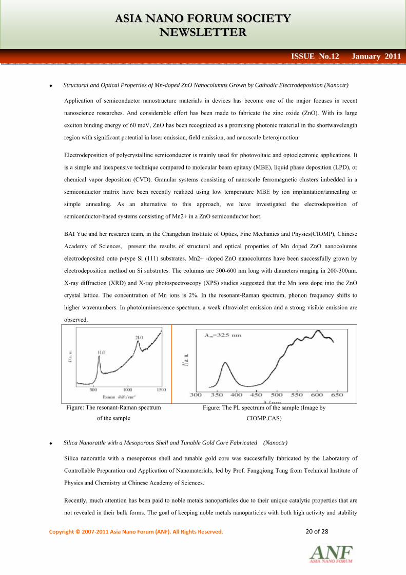
Structural and Optical Properties of Mn-doped ZnO Nanocolumns Grown by Cathodic Electrodeposition (Nanoctr)
Application of semiconductor nanostructure materials in devices has become one of the major focuses in recent
nanoscience researches. And considerable effort has been made to fabricate the zinc oxide (ZnO). With its large
exciton binding energy of 60 meV, ZnO has been recognized as a promising photonic material in the shortwavelength
region with significant potential in laser emission, field emission, and nanoscale heterojunction.
Electrodeposition of polycrystalline semiconductor is mainly used for photovoltaic and optoelectronic applications. It
is a simple and inexpensive technique compared to molecular beam epitaxy (MBE), liquid phase deposition (LPD), or
chemical vapor deposition (CVD). Granular systems consisting of nanoscale ferromagnetic clusters imbedded in a
semiconductor matrix have been recently realized using low temperature MBE by ion implantation/annealing or
simple annealing. As an alternative to this approach, we have investigated the electrodeposition of
semiconductor-based systems consisting of Mn2+ in a ZnO semiconductor host.
BAI Yue and her research team, in the Changchun Institute of Optics, Fine Mechanics and Physics(CIOMP), Chinese
Academy of Sciences, present the results of structural and optical properties of Mn doped ZnO nanocolumns
electrodeposited onto p-type Si (111) substrates. Mn2+ -doped ZnO nanocolumns have been successfully grown by
electrodeposition method on Si substrates. The columns are 500-600 nm long with diameters ranging in 200-300nm.
X-ray diffraction (XRD) and X-ray photospectroscopy (XPS) studies suggested that the Mn ions dope into the ZnO
crystal lattice. The concentration of Mn ions is 2%. In the resonant-Raman spectrum, phonon frequency shifts to
higher wavenumbers. In photoluminescence spectrum, a weak ultraviolet emission and a strong visible emission are
observed.
Silica Nanorattle with a Mesoporous Shell and Tunable Gold Core Fabricated (Nanoctr)
Silica nanorattle with a mesoporous shell and tunable gold core was successfully fabricated by the Laboratory of
Controllable Preparation and Application of Nanomaterials, led by Prof. Fangqiong Tang from Technical Institute of
Physics and Chemistry at Chinese Academy of Sciences.
Recently, much attention has been paid to noble metals nanoparticles due to their unique catalytic properties that are
not revealed in their bulk forms. The goal of keeping noble metals nanoparticles with both high activity and stability

Copyright © 2007‐2011 Asia Nano Forum (ANF). All Rights Reserved. 21 of 28
AASSIIAA NNAANNOO FFOORRUUMM SSOOCCIIEETTYY NNEEWWSSLLEETTTTEERR
ISSUE No.12 January 2011
Figure: Image by TIPC, CAS
Figure: Silica Nanorattle as drug delivery system for Liver
have been pursued by materials scientists for many years. The
encapsulation of metal core into hollow nanosphere with
mesoporous shell provides an effective strategy to resolve this
problem.
This research group has fabricated a unique nanostructure with
independent intellectual property, silica nanorattle, which has a
hollow cavity and a mesoporous shell. The sphere sizes, the
middle cavities’ volume, the thickness of mesoporous shell can
be controlled precisely. Moreover, the mesoporous shell allows the diffusion of small active molecules in and out of
the nanosphere. Meanwhile, the inside of the silica nanorattle has plenty of reactive groups, which can be used as in
situ reducing agent and stabilizer for the growth of noble metal core. Taking advantage of these reactive groups and
the hollow cavity, the researchers fabricated size-tunable gold core in the hollow cavity by using the silica nanorattle
as ideal nanoreactor.
This kind of gold core silica nanorattle was successfully applied in the catalytic reduction of 2-nitroaniline as a model
reaction, showing great activity after catalytic reaction for 5 cycles. In addition, the synthesis method is quite simply
and easy to scale up, and the strategy can be extended to fabricated hollow silica nanoparticles with other noble metal
cores and noble metal nanoparticles on other silica nanostructures.
The relevant results have been published in a recent online issue of Advanced Materials titled by 'A Silica Nanorattle
with a Mesoporous Shell: An Ideal Nanoreactor for the Preparation of Tunable Gold Cores' (Adv. Mater.,
DOI:10.1002/adma.201002277). The relevant work has been applied for a Chinese patent.
Silica Nanorattle as a New Drug Delivery System Developed (Nanoctr)
The research group headed by Prof. TANG
Fangqiong of Technical Institute of Physics and
Chemistry, Chinese Academy of Sciences has
developed a new drug delivery system for cancer
therapy using silica nanorattle as drug carrier.
To solve the nonspecific toxicity anti-tumor drugs,
the researchers designed silica nanorattle with
high drug loading and controlled drug release as
drug carrier. For liver cancer therapy, the silica
nanorattle encapsulated docetaxel showed higher therapeutic efficacy and lower systematic toxicity compared with
current clinical formulation of Taxotere. The drug carrier itself had high biocompatibility with single and repeated

AASSIIAA NNAANNOO FFOORRUUMM SSOOCCIIEETTYY NNEEWWSSLLEETTTTEERR
ISSUE No.12 January 2011
Copyright © 2007‐2011 Asia Nano Forum (ANF). All Rights Reserved. 22 of 28
dose administration and can be excrete from the body. These findings are a great stride for inorganic
nanoparticle-based drug delivery systems, and have potentials to revolutionize the diagnosis and treatment of cancer.
The works published on ACS Nano and Biomaterials were supported by National High-tech R&D Program of China
(863 Program) and National Natural Science Foundation of China.
Patent of Suzhou Institute of Nano-tech and Nano-bionics Wins Gold Prize of 7th China International Patent &
Famous-Brand Expo (Nanoctr)
A patent “a PIN type nuclear detector and its preparation methods” of associated professor Dr. LU Min from Suzhou
Institute of Nano-tech and Nano-bionics has been awarded gold prize on the seventh China International Patent and
Famous-Brand Expo held in Wu Xi of Jiang Su province Nov.6-8 2010.
This patent aims at designing and fabricating PIN type nuclear detectors based on GaN, which has wider band gap
than traditional semiconductor detectors such as Si, GaAs, CZT, etc.. So it doesn’t need to reduce noise signal by
cooling, and it can work at room temperature. Also it has stronger radiation resistance compared with traditional
semiconductor detectors. Therefore it has broad applications in nuclear medicine, nuclear imaging, and advanced
nuclear reactors neutron detection, and so on. This detector has been in R&D, and the prototype device has been
successfully fabricated by Dr. Lu Min and his group. This detector has emerged with some better performance than
conventional semiconductor detectors.
GaN nuclear radiation detectors are the core component of the XRF equipments, nuclear medicine imaging systems
such as X-ray imaging, PET and SPET machines, etc.. The excellent radiation hardness and corrosion resistance can
greatly improve the performance of nuclear power control systems, which would result in better safety and higher
using efficiency of nuclear fuel. The patent leads to not only good economic benefits, but also very prominent social
benefits. It has significant impact on energy conservation and emission reduction. In the application of medical
imaging system, it can greatly improve imaging quality and greatly reduce radiation dose absorbed by patients and
doctors, and the doctors can also more easily observed the patients’ lesions with subtle pathological change. This is
important to improve the diagnostic capabilities of medical imaging in China.
3D DNA Nanostructure-Based Biosensor Platform for DNA Detection Developed (Nanoctr)
A 3D DNA nanostructure-based biosensor platform for DNA detection has been developed to realize highly sensitive
and selective DNA detection in biological fluids and enhance sequence specificity for SNP typing.
Biosensor is a device for the detection of an analyte that combines a biological component with a physicochemical
detector component. The traditional DNA sensors are constructed on the basis of a classic, linear DNA probe-based
two-step assembly strategy that is insufficient to control the inter-probe and probe–target interactions on surfaces. To
improve the recognition abilities of such heterogeneous surface probes, a 3D DNA nanostructure-based sensor
platform came into being.

AASSIIAA NNAANNOO FFOORRUUMM SSOOCCIIEETTYY NNEEWWSSLLEETTTTEERR
ISSUE No.12 January 2011
Copyright © 2007‐2011 Asia Nano Forum (ANF). All Rights Reserved. 23 of 28
Because of the unparalleled self-assembly abilities of DNA molecules, DNA nanotechnology demonstrates promising
application in constructing biosensors of versatile structures. The strategy to design and construct 3D nanostructured
recognition probes on a surface provides a significantly enhanced spatial positioning range and accessibility of the
probes on a surface over previously reported linear or stem-loop probe structures.
The nanostructure-based sensor platform was co-developed by Shanghai Institute of Applied Physics under Chinese
Academy of Sciences and Arizona State University of America. The main findings were published as the cover article
in Advanced Materials, 2010, 22, 4754-4758.
Iran
Newly-Produced Nanofibers Heal, Regenerate Bone Cells (INIC)
TEHRAN (INIC)- Researchers at College of Science of University of Tehran in tight collaboration with their
colleagues at Stem Cell Technology Research Center, Iran, exploited nanofibrous poly (lactic acid) scaffolds coated
with hydroxyapatite nanoparticles for bone tissue engineering applications. "In the conducted research, nanofibrous
poly (lactic acid) scaffolds were synthesized via electrospinning in the first phase. The mentioned scaffolds underwent
plasma processing for superficial modifications. Prior to that, nanohydroxyapatite (n-HA) was coated on the
scaffolds," Ehsan Seyejafari, the chief researcher of the study, said to the news service of INIC. According to
Seyejafari, the synthesis procedure of the discussed scaffolds is so simple and cost-effective that their production on an
industrial scale looks very likely. Coating nanohydroxyapatite particles upon the nanofibers provides direct contact
onto cells and surrounding tissues. As a result, their bioactivity effect for osteogenic repair and regeneration is
enhanced. "Electron microscopic analyses revealed that all the scaffolds possessed nanofibrous structures of planar
type and the superficial modifications brought about no changes on their development," Seyejafari reiterated,
elaborating on the procedure of the research. "Furthermore, nanoparticles were perfectly coated upon nanofibers'
surfaces and did not disturb scaffold porosity. FTIR ascertained the presence of nanohydroxyapatite particles attached
to nanofibers by the relevant peaks. Nanofibers' surfaces became highly hydrophilic and their contact angle inclined
towards zero." "Cell growth and multiplication tests confirmed biocompatibility of the nanostructures. In vitro
investigations in mice demonstrated that the fabricated scaffolds are capable of simulating osteogenesis and forming
the bony baffles," he concluded. An elaborated report on the researchers' findings has been published in the Journal of
Biomacromolecules, vol. 11, pages 3118-3125, 2010.
Lead Ions Detected in Water by New Low-Cost Nanosensors (INIC)
TEHRAN (INIC) - The Iranian researchers at Razi Univeristy of Kermanshah made a low-cost nanosensor for
detection of the trace of toxic lead ion in water and aqueous solutions by means of gold nanoparticles. This nanosensor,
having rapid operation, is produced by supersensitive azacrown ether-functionalized gold nanoparticles with no need
to expensive materials and methods. Noting that the aforementioned nanosensor shows the result without using DNA,
dye molecules, enzymes, or any other additive, Dr. Abdolhamid Alizadeh, faculty member at Nanoscience and
Nanotechnology Research Center (NNRC), faculty of chemistry, Razi University of Kermanshah said to the INIC

AASSIIAA NNAANNOO FFOORRUUMM SSOOCCIIEETTYY NNEEWWSSLLEETTTTEERR
ISSUE No.12 January 2011
Copyright © 2007‐2011 Asia Nano Forum (ANF). All Rights Reserved. 24 of 28
news service that this nanosensor operates just ocularly. "The detection precision of this nanosensor is of nanomolar, it
operates fast and more importantly, it benefits from low cost fabrication technology," he added. "First, thiol-bearing
arms are added to a receiver able of forming complex with metals. Then, they are bonded with gold nanoparticles
surface, which are presynthesized, via thiol-gold bond. Lastly, the performance of sensor is analyzed and validated by
studying changes in optical properties of nanoparticles before and after addition of aqueous solution containing various
metallic ions," he said, explaining about the procedure of the research. Alizadeh also referred to a Singaporean
company's interest in commercializing the aforesaid nanosensor, and noted, "The initial consultations with the
company are underway." For more details see Nanotechnology-IOP, vol. 21, p. 315503, 2010.
New Magnetic Nanoparticles Easily Remove Organic Pollutants (INIC)
TEHRAN (INIC)- New type of Magnetic nanoparticles of Fe3O4 were synthesized at Tarbiat Modares University
(TMU) in Iran through an appropriate, simple, repetitive method with the potential to be mass-produced at large scales
for the removal of different organic and inorganic contaminations. Using magnetic nanoparticles is one of the
extraction and separation methods aimed at concentrating and separating or removing high contents of various organic
and inorganic contaminations. The advantage of using magnetic nanoparticles is that they could be absorbed by an
external magnetic field, an interesting feature for chemical analysis, so there would be no need to centrifuge and filter
samples after their extraction at all. "These magnetic nanoparticles could be applied as a new brand absorber for
extraction and measurement of different analytes and also for the optimum removal of pollutants", Yadollah Yamini,
chemistry professor at TMU, said in an interview with INIC news service. Dr. Yamini and his colleagues managed to
design a suitable reactor for the synthesis of Fe3O4 magnetic nanoparticles via co-precipitation method and to modify
nanoparticles surface in order to extract and remove contaminations. They also extracted and analyzed traces of
metallic ions and drugs in aqueous mediums and biological samples. Lastly, they successfully removed metallic ions
and pigments from textile industry wastewaters. "There is a possibility for synthesizing pure or silica-coated magnetic
nanoparticles at large scales at present. Our research group is willing to design appropriate absorbers for removal of
pollutants from industrial wastewaters," he added. The details of this study are available at Journal of the Iranian
Chemical Society, volume 7, pages 130-144, 2010.
Singapore
ALD for Surface Coating on Nanowires (NTU)
Atomic layer deposition (ALD) is a vapor-phase thin film growth technique allowing atomic-scale thickness and
uniformity control. It is based on a sequence of two self-limiting reactions between gas phase precursor molecules and
a solid surface. Unlike CVD, ALD keeps the precursors separated from each other in sequenced growth cycles, thus
preventing unwanted gas phase reactions. ALD is traditionally of industrial interest for deposition of high-k oxides
(HfO2 and Al2O3) and 3-D trench capacitors. Recently ALD starts to be widely used for surface coating of
nanostructures. In this application, it is especially advantageous because it is capable of creating conformal coating to
very high aspect ratio geometries (for example see the figure) and even porous structures.
Copyright © 2007‐2011 Asia Nano Forum (ANF). All Rights Reserved. 25 of 28
AASSIIAA NNAANNOO FFOORRUUMM SSOOCCIIEETTYY NNEEWWSSLLEETTTTEERR
ISSUE No.12 January 2011
Nanowires (NWs), diameter ~10100 nm, length 15 m, are being regarded
as a promising candidate for various applications in optoelectronics, sensors,
and energy generation and storage devices. The group lead by Fan Hongjin
in School of Physical & Mathematical Sciences, Nanyang Technological
University, is applying ALD for surface coating of inorganic nanowires, both
random-oriented and vertical aligned. Their special interest is the application
of ALD in nanowire-based energy storage devices with the aim of
significantly improving the charge/discharge cycle numbers. In these devices, ALD thin coating can provide surface
passivation, preventing the active NW electrode material from mechanical or chemical deterioration. It is known that
batteries and supercapacitors based on metal-oxide NWs generally exhibit larger capacity compared to powder
electrodes due to the direct current flow in NWs. However, NWs have limited cycling stability: the nanostructure will
generally collapse after ~3050 cycles. A thin coating of the surfaces of the NW electrodes will help to better
accommodate the volume expansion, restrict the growth of thick solid electrolyte interface films, and thus benefit the
cycle performance.
Fan's group is also using ALD for tuning the luminescence of ZnO nanomaterials, for which a thin dielectric layer not
only isolates the sensitive NW surface from air ambient, but also enhances the light emission by eliminating the
unwanted quenching process.
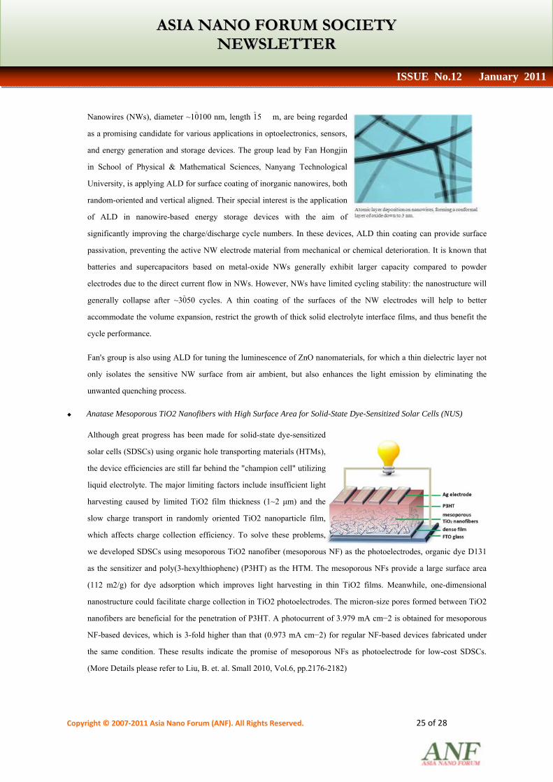
Anatase Mesoporous TiO2 Nanofibers with High Surface Area for Solid-State Dye-Sensitized Solar Cells (NUS)
Although great progress has been made for solid-state dye-sensitized
solar cells (SDSCs) using organic hole transporting materials (HTMs),
the device efficiencies are still far behind the "champion cell" utilizing
liquid electrolyte. The major limiting factors include insufficient light
harvesting caused by limited TiO2 film thickness (1~2 μm) and the
slow charge transport in randomly oriented TiO2 nanoparticle film,
which affects charge collection efficiency. To solve these problems,
we developed SDSCs using mesoporous TiO2 nanofiber (mesoporous NF) as the photoelectrodes, organic dye D131
as the sensitizer and poly(3-hexylthiophene) (P3HT) as the HTM. The mesoporous NFs provide a large surface area
(112 m2/g) for dye adsorption which improves light harvesting in thin TiO2 films. Meanwhile, one-dimensional
nanostructure could facilitate charge collection in TiO2 photoelectrodes. The micron-size pores formed between TiO2
nanofibers are beneficial for the penetration of P3HT. A photocurrent of 3.979 mA cm−2 is obtained for mesoporous
NF-based devices, which is 3-fold higher than that (0.973 mA cm−2) for regular NF-based devices fabricated under
the same condition. These results indicate the promise of mesoporous NFs as photoelectrode for low-cost SDSCs.
(More Details please refer to Liu, B. et. al. Small 2010, Vol.6, pp.2176-2182)

Copyright © 2007‐2011 Asia Nano Forum (ANF). All Rights Reserved. 26 of 28
AASSIIAA NNAANNOO FFOORRUUMM SSOOCCIIEETTYY NNEEWWSSLLEETTTTEERR
ISSUE No.12 January 2011
Ref: Date 0 Ref: Date 7 Ref: Date 21
Hyperthermia:
Date 0
Hyperthermia:
Date 7
Hyperthermia:
Date21
Vietnam
Successful experiment on cancer hyperthermia using iron nanoparticles: a mouse study. (VAST)
A joint research by a group from Institute of Materials Science and Hanoi University of Science has performed
successfully an in-vivo treatment of solid tumor (Sarcoma 180) on Swiss mice by using magnetic hyperthermia with
iron oxide thermoseed. Ferrofluid of magnetite nanoparticles in core and a copolymer capping material was
synthesized inductive heating characterized, so that a dose of 0.5mg/ml was chosen to generate a temperature of ca.
48oC for the tumor of size around 6x6mm. 4 groups of treated mice were recovered (tumor first shrinked and then
disappeared) after 20 days, whereas other 4 groups of reference mice have died up to 40 days (see pictures).
AASSIIAA NNAANNOO FFOORRUUMM SSOOCCIIEETTYY NNEEWWSSLLEETTTTEERR
ISSUE No.12 January 2011
Copyright © 2007‐2011 Asia Nano Forum (ANF). All Rights Reserved. 27 of 28
NEW PUBLICATION
China
1. Zheng K, Wang CC, and Cheng YQ et al., “Electron-beam-assisted Superplastic Shaping of Nan scale Amorphous
Silica” ATURE COMMUNICATIONS, 1: Art. No. 24 JUN 2010
2. Bay YH, Zhang Y, and Zhang JP et al., “Repeated Administrations of Carbon Nanotubes in Male Mice Cause Reversible
Testis Damage without Affecting Fertility” , NATURE NANOTECHNOLOGY, 5 (9): 683-689 SEP 2010
Vietnam
1. A special issue on Nanotechnology in Vietnam has been published in International Journal of Nanotechnology Vol. 8,
Nos 3/4/5 2011, which contains 50 papers and Editorial by Prof. Le Van Hong.

Copyright © 2007‐2011 Asia Nano Forum (ANF). All Rights Reserved. 28 of 28
AASSIIAA NNAANNOO FFOORRUUMM SSOOCCIIEETTYY NNEEWWSSLLEETTTTEERR
ISSUE No.12 January 2011
EVENTS
Date Avenue Events
Feb. 7-11, Wellington, New Zealand
The 5th International Conference on Advanced Materials and Nanotechnology
http://www.macdiarmid.ac.nz
Feb.16-18, Tokyo, Japan nano tech 2011 (10th International Nanotechnology Exhibition & Conference) http://www.nanotechexpo.jp/en/
2011 Beijing, China MEMSIC Cup, The Second International Contest of Applications in
Nano-micro Technology (iCAN'11)
www.iCAN-contest.com
Feb.26-28 Singapore 2011 2nd International Conference on Mechanical, Industrial, and Manufacturing
Technologies (MIMT 2011)
http://www.iacsit.org/mimt/
Mar.02-04 Tokyo, Japan 3rd Annual Asia TIDES: Oligonucleotide and Peptide Research, Technology and
Product Development
website: http://www.ibclifesciences.com/AsiaTIDES/overview.xml
Mar.24-25 Pathumthani,
Thailand
Joint Symposium on Nanobiotechnology - Organized by KRIBB (KOREA) and
NANOTEC (THAILAND)
http://www.nanotec.or.th/en/
May.12-17 Mashhad, Iran 5th Int'l Symposium on Advances in Science, Technology
www.5thsastech.khi.ac.ir
May.10-12 Isfahan, Iran 2nd Int'l Conference on Materials Heat Treatment
http://icmh.ir/
Jun.7-9 Shanghai,
China
Nanotech China
http://www.nanotechchina.org/
Jun.26-Jul.1, 2011,
Singapore
ICMAT 2011 (International Conference on Materials for Advanced Technologies)
http://www.mrs.org.sg/icmat2011
Aug.24-26 Seoul, Korea NANO KOREA 2011, The 9th International Nanotech Exhibition in Korea
http://www.nanokorea.or.kr/Eng/Introduction/Introduction.asp
Oct. , 1st week Taipei, Taiwan Taiwan Nano 2011 Conference & Exhibition