as3501 as3502 data sheet low power ambient noise
TRANSCRIPT

AS3501 AS3502 Low Power Ambient Noise-Cancel l ing Speaker Dr iver
www.austriamicrosystems.com Revision 1.13 1 - 45
Data Shee t
1 General DescriptionThe AS3501/02 are speaker driver with Ambient Noise Cancelling function for headsets, headphones or ear pieces. It is intended to improve quality of e.g. music lis-tening, a phone conversation etc. by reducing back-ground ambient noise.
The fully analog implementation allows the lowest power consumption, lowest system BOM cost and most natural received voice enhancement otherwise difficult to achieve with DSP implementations. The device is designed to be easily applied to existing architectures.
An internal OTP-ROM can be optionally used to store the microphones gain calibration settings.
The AS3501/02 can be used in different configurations for best trade-off of noise cancellation, required filtering functions and mechanical designs.
The simpler feed-forward topology is used to effectively reduce low frequency background noise. The feed-back topology with either 1 or 2 filtering stages can be used to reduce noise for a larger frequency range, and to even implement transfer functions like speaker equalization, Baxandall equalization, high/low shelving filter and to set a predefined loop bandwidth.
The filter loop is optimized by the user for specific head-set electrical and mechanical designs by dimensioning simple R, C components.
Most headset implementations will make use of a single noise detecting microphone. Two microphones could be used to allow for increased flexibility of their location in the headset mechanical design. Using the bridged mode allows to even drive high impedance headsets.
2 Key FeaturesMicrophone Input 128 gain steps @0.375dB and MUTE with AGC
differential, low noise microphone amplifier
single ended or differential mode
supply for electret microphone
MIC gain OTP programmable
High Efficiency Headphone Amplifier 2x34mW, 0.1% THD @ 16Ω, 1.5V supply,
100dB SNR
bridged mode for e.g. 300Ω loads
click and pop less start-up and mode switching
Line Input volume control via serial interface or volume pin
64 steps @ 0.75dB and MUTE, pop-free gain setting
single ended stereo or mono differential mode
ANC processing feed-forward cancellation
feed-back cancellation with filter loop transfer func-tion definable via simple RC components
simple in production SW calibration
12-30dB noise reduction (headset dependent)
10-2000Hz wide frequency active noise attenuation (headset dependent)
Monitor Function for assisted hearing, i.e. to monitor announcements
fixed (OTP prog.) ambient sound amplification to compensate headphone passive attenuation
volume controlled ambient sound amplification mixed with fixed (OTP prog.) attenuation of LineIn
Incremental Functions ANC with or without music on the receiving path
improved dynamic range playback
simple and low cost single noise detection micro-phone implementation
OTP ROM for automatic trimming during production
Performance Parameter 5/3.8mA @ 1.5V stereo/mono ANC; <1uA quiescent
extended PSRR for 217Hz
Interfaces 2 wire serial control mode & volume inputs
calibration via Line-In or 2-wire serial interface
single cell or fixed 1.0-1.8V supply with internal CP
Package AS3501 QFN24 [4x4mm] 0.5mm pitch
AS3502 QFN32 [5.x5mm] 0.5mm pitch
3 ApplicationsEar pieces, Headsets, Hands-Free Kits, Mobile Phones, Voice Communicating Devices
ams A
G
Technica
l conten
t still
valid

www.austriamicrosystems.com Revision 1.13 2 - 45
AS3501 AS3502 1v2Data Sheet
Figure 1. AS3501 Feed Forward ANC Block Diagram
Figure 2. AS3502 Feed-Back Block Diagram
ams A
G
Technica
l conten
t still
valid

www.austriamicrosystems.com Revision 1.13 3 - 45
AS3501 AS3502 1v2Data Sheet
Contents1 General Description ............................................................................................................................1
2 Key Features .......................................................................................................................................1
3 Applications ........................................................................................................................................1
4 Pinout ...................................................................................................................................................4
4.1 Pin Assignment ..............................................................................................................................................4
4.2 Pin Description ...............................................................................................................................................5
5 Absolute Maximum Ratings ...............................................................................................................6
6 Electrical Characteristics ...................................................................................................................7
7 Typical Operating Characteristics .....................................................................................................9
8 Detailed Description .........................................................................................................................13
8.1 Audio Line Input ...........................................................................................................................................13
8.2 Microphone Input .........................................................................................................................................14
8.3 Headphone Output .......................................................................................................................................16
8.4 Operational Amplifier ...................................................................................................................................17
8.5 SYSTEM ......................................................................................................................................................18
8.6 VNEG Charge Pump ...................................................................................................................................20
8.7 OTP Memory & Internal Registers ...............................................................................................................20
8.8 2-Wire-Serial Control Interface ....................................................................................................................23
9 Register Description .........................................................................................................................26
10 Application Information ..................................................................................................................36
11 Package Drawings and Markings ..................................................................................................40
12 Ordering Information ......................................................................................................................43
ams A
G
Technica
l conten
t still
valid

www.austriamicrosystems.com Revision 1.13 4 - 45
AS3501 AS3502 1v2Data Sheet
4 Pinout4.1 Pin AssignmentPlease observe that pin assignment may change in preliminary data sheets.
Figure 3. Pin Assignments (Top View)
must NOT be connected to GND or AGND!CAUTION: Exposed pad must be connected to VNEG or left unconnected. Exposed pad
ams A
G
Technica
l conten
t still
valid

www.austriamicrosystems.com Revision 1.13 5 - 45
AS3501 AS3502 1v2Data Sheet
4.2 Pin DescriptionPlease observe that pin description may change in preliminary data sheets.
Table 1. Pin Description for AS3501 AS3502
AS3501 AS3502 Pin Name Type Description
24 1 IOP1L ANA IN Filter OpAmp1 Input Left Channel
- 2 QLINL ANA OUT Line In Gain Stage Output Left Channel
1 3 QMICL ANA OUT MIC Gain Stage Output Right Channel
2 4 AGND ANA IN Analog Reference
3 5 LINL ANA INDIG IN
Line In Left ChannelDuring Application Trim Mode Write – CSDADuring Application Trim Mode Burn - VNEG
4 6 LINR ANA INDIG IO
LineIn Right ChannelDuring Application Trim Mode Write – CSCLDuring Application Trim Mode Burn - Clock
5 7 VOL_CSDA MIXED IOSerial Interface DataADC Input for volume regulation
6 8 MODE_CSCL DIG INMode Pin (Power Up/Down, Monitor)Serial Interface Clock
7 9 MICL ANA IN Microphone In Left Channel
8 10 ILED ANA OUT Current Output for on-indication LED
9 11 MICS ANA OUT Microphone Supply
10 12 MICR ANA IN Microphone Input Right Channel
11 13 QMICR ANA OUT MIC Gain Stage Output Right Channel
- 14 QLINR ANA OUT Line In Gain Stage Output Right Channel
12 15 IOP1R ANA IN FilterOpAmp1 Input Right Channel
13 16 QOP1R ANA IN Filter OpAmp1 Output Right Channel
- 17 IOP2R ANA IN Filter OpAmp2 Input Right Channel
- 18 QOP2R ANA OUT Filter OpAmp2 Output Right Channel
14 19 VSS SUP IN Core and Periphery Circuit VSS Supply
15 20 HPL ANA OUT Headphone Output Left Channel
- 21 HPVSS SUP IN Headphone VSS Supply
16 22 HPR ANA OUT Headphone Output Right Channel
17 23 HPVDD SUP IN Headphone VDD Supply
18 24 VBAT SUP IN VNEG ChargePump Positive Supply
- 25 n.c. -
19 26 CPP ANA OUT VNEG ChargePump Flying Capacitor Positive Terminal
20 27 GND GND VNEG ChargePump Negative Supply
21 28 CPN ANA OUT VNEG ChargePump Flying Capacitor Negative Terminal
22 29 VNEG SUP IO VNEG ChargePump Output
- 30 QOP2L ANA OUT Filter OpAmp2 Output Left Channel
- 31 IOP2L ANA IN Filter OpAmp2 Input Left Channel
23 32 QOP1L ANA OUT Filter OpAmp1 Output Right Channel
25 33 Exposed Pad: connect to VNEG or leave it unconnected
ams A
G
Technica
l conten
t still
valid

www.austriamicrosystems.com Revision 1.13 6 - 45
AS3501 AS3502 1v2Data Sheet
5 Absolute Maximum RatingsStresses beyond those listed in Table 2 may cause permanent damage to the device. These are stress ratings only, and functional operation of the device at these or any other conditions beyond those indicated in Electrical Character-istics on page 7 is not implied. Exposure to absolute maximum rating conditions for extended periods may affect device reliability. The device should be operated under recommended operating conditions.Table 2. Absolute Maximum Ratings
Parameter Min Max Units Comments
Reference Ground Defined as in GND
Supply terminals -0.5 2.0 V Applicable for pin VBAT, HPVDD
Ground terminals -0.5 0.5 V Applicable for pins AGND
Negative terminals -2.0 0.5 V Applicable for pins VNEG, VSS, HPVSS
Voltage difference at VSS terminals -0.5 0.5 V Applicable for pins VSS, HPVSS
Pins with protection to VBAT VNEG-0.5
5.0VBAT+0.5 V Applicable for pins CPP, CPN
Pins with protection to HPVDD VSS-0.5
5.0HPVDD+0.5 V
Applicable for pins LINL/R, MICL/R, ILED, HPR, HPL, QMICL/R, QLINL/R,
IOPx, QOPx
other pins VSS-0.5 5 applicable for pins MICS, VOL_CSDA,
MODE_CSCL
Input Current (latch-up immunity) -100 100 mA Norm: JEDEC 17
Continuous Power Dissipation (T A = +70ºC)
Continuous Power Dissipation - 200 mW PT1 for QFN16/24/32 package
1. Depending on actual PCB layout and PCB used
Electrostatic Discharge
Electrostatic Discharge HBM +/-2 kV Norm: JEDEC JESD22-A114C
Temperature Ranges and Storage Conditions
Junction Temperature +110 ºC
Storage Temperature Range -55 +150 ºC
Humidity non-condensing 5 85 %
Moisture Sensitive Level 3 Represents a max. floor life time of 168h
Package Body Temperature 260 °C
The reflow peak soldering temperature (body temperature) specified is in
accordance with IPC/JEDEC J-STD-020“Moisture/Reflow Sensitivity
Classification for Non-Hermetic Solid State Surface Mount Devices”.
ams A
G
Technica
l conten
t still
valid

www.austriamicrosystems.com Revision 1.13 7 - 45
AS3501 AS3502 1v2Data Sheet
6 Electrical CharacteristicsVBAT = 1.0V to 1.8V, TA = -20ºC to +85ºC. Typical values are at VBAT = 1.5V, TA = +25ºC, unless otherwise specified.
All limits are guaranteed. The parameters with min and max values are guaranteed with production tests or SQC
(Statistical Quality Control) methods. Table 3. Electrical Characteristics
Symbol Parameter Condition Min Max Unit
TA Ambient Temperature Range -20 +85 °C
Supply Voltages
GND Reference Ground 0 0 V
VBAT, HPVDD Battery Supply Voltage
normal operation MODE pin high 1.0 1.8 V
two wire interface operation 1.4 1.8 V
VNEG ChargePump Voltage -1.8 -0.7 V
VSS Analog neg. Supply VoltagesHPVSS, VSS, VNEG -1.8 -0.7 V
VDELTA-Difference of Ground
SuppliesGND, AGND
To achieve good performance, the negative supply terminals should be connected to low impedance ground
plane.
-0.1 0.1 V
VDELTA--Difference of Negative
SuppliesVSS, VNEG, HPVSS
Charge pump output or external supply -0.1 0.1 V
VDELTA+ Difference of Positive Supplies VBAT-HPVDD -0.25 0.25 V
other pins
VMICS Microphone Supply Voltage MICS 0 3.6 V
VHPVDD pins with diode to HPVDD MICL/R, ILED, HPR, HPL, QMICL/R, QLINL/R, IOPx, QOPx VSS HPVDD V
VVBAT pins with diode to VBAT CPP, CPN VNEG VBAT V
VCONTROL Control Pins MODE_CSCL, VOL_CSDA VSS 3.7 V
VTRIMLine Input & Application Trim
Pins LINL, LINR VNEG -0.5or -1.8
HPVDD +0.5or 1.8 V
Symbol Parameter Condition Min Typ Max Unit
Block Power Requirements @ 1.5V VBAT
IOFF Off mode current MODE pin low, device switched off 1 µA
ISYS Reference supply current bias generation, oscillator, ILED current sink, ADC6 0.25 mA
ILIN LineIn gain stage current no signal, stereo 0.64 mA
IMIC Mic gain stage current no signal, stereo 2.10 mA
IHP Headphone stage current no signal 1.70 mA
IVNEG VNEG charge pump current no load 0.25 mA
IMICS MICS charge pump current no load 0.06 mA
IMIN minimal supply current sum of all above blocks 5.00 mA
ams A
G
Technica
l conten
t still
valid

www.austriamicrosystems.com Revision 1.13 8 - 45
AS3501 AS3502 1v2Data Sheet
IOP1 OP1 supply current no load 0.64 mA
IOP2 OP2 supply current no load 0.64 mA
IILED ILED current sink current 100% duty cycle 2.50 mA
IMICB Microphone bias current 200uA per microphone via charge pump 1.30 mA
Symbol Parameter Condition Min Typ Max Unit
ams A
G
Technica
l conten
t still
valid

www.austriamicrosystems.com Revision 1.13 9 - 45
AS3501 AS3502 1v2Data Sheet
7 Typical Operating CharacteristicsVBAT = +1.5V, TA = +25ºC, unless otherwise specified.
Figure 4. LIN to HPH: THD+N versus Output Power
Figure 5. VNEG Charge Pump
THD+N vs POUT - 32Ω - stereo single ended
0,01
0,1
1
0 5 10 15 20 25 30 35 40
Pout [mW]T
HD
+N [%
]
VBAT=1.8VVBAT=1.5VVBAT=1.0V
THD+N vs POUT - 16Ω - single ended stereo
0,01
0,1
1
0 10 20 30 40 50 60
Pout [mW]
TH
D+N
[%]
VBAT=1.8VVBAT=1.5VVBAT=1.0V
THD+N vs POUT - 32Ω - bridged-tied load
0,01
0,1
1
0 10 20 30 40 50 60 70 80 90 100 110 120 130
Pout [mW]
TH
D+N
[%]
VBAT=1.8V
VBAT=1.5V
VBAT=1.0V
THD+N vs POUT - 64Ω - bridged-tied load
0,01
0,1
1
0 10 20 30 40 50 60 70 80 90
Pout [mW]
TH
D+N
[%]
VBAT=1.8V
VBAT=1.5V
VABT=1.0V
VNEG CP Voltage vs Load Current
-1,8
-1,6
-1,4
-1,2
-1,0
-0,8
-0,6
-0,4
-0,2
0,0
0 50 100 150 200
I_VNEG [mA]
V_V
NE
G [V
]
VBAT=1.0V
VBAT=1.5V
VBAT=1.8V
VNEG CP Efficiency
50
55
60
65
70
75
80
85
90
95
100
0 20 40 60 80 100 120 140 160 180 200
I_VNEG [mA]
Eff
[%]
VBAT=1.0V
VBAT=1.5V
VBAT=1.8V
ams A
G
Technica
l conten
t still
valid

www.austriamicrosystems.com Revision 1.13 10 - 45
AS3501 AS3502 1v2Data Sheet
Figure 6. Microphone Supply Generation
Figure 7. ILED Current Sink (100% PWM setting)
MICS Charge Pump
0
0,5
1
1,5
2
2,5
3
3,5
0 500 1000 1500 2000
I_MICS [uA]
V_M
ICS
[V]
VBAT=1.8V
VBAT=1.5V
VABT=1.0V
I_MICS vs dI_VBAT
0
1000
2000
3000
4000
5000
6000
7000
0 500 1000 1500 2000
I_MICS [uA]
dI_V
BA
T [u
A]
VBAT=1.8V
VBAT=1.5V
VBAT=1.0V
V_MICS vs V_VBAT
1,5
1,7
1,9
2,1
2,3
2,5
2,7
2,9
3,1
3,3
3,5
0,9 1,0 1,1 1,2 1,3 1,4 1,5 1,6 1,7 1,8
VBAT [V]
V_M
ICS
[V]
I_MCS = 0.0uA
I_MICS = 600uA
R_MICS_Switch vs V_VBAT
40
50
60
70
80
90
100
110
120
130
140
0,9 1,0 1,1 1,2 1,3 1,4 1,5 1,6 1,7 1,8
VBAT [V]
R_M
ICS
_Sw
itch
[Ω
]
ILED Current
0,0
0,5
1,0
1,5
2,0
2,5
3,0
0,0 0,1 0,2 0,3 0,4 0,5
V (ILED-VNEG) [V]
I (IL
ED
) [m
A] ILED (Vbat=1.8V)
ILED (Vbat=1.5V)
ILED (Vbat=1.0V)
ILED Current
0,0
0,5
1,0
1,5
2,0
2,5
3,0
0,0 0,5 1,0 1,5 2,0 2,5 3,0
V (ILED-VNEG) [V]
I (I
LED
) [m
A]
ILED (Vbat=1.8V)
ILED (Vbat=1.5V)
ILED (Vbat=1.0V)
ams A
G
Technica
l conten
t still
valid
www.austriamicrosystems.com Revision 1.13 11 - 45
AS3501 AS3502 1v2Data Sheet
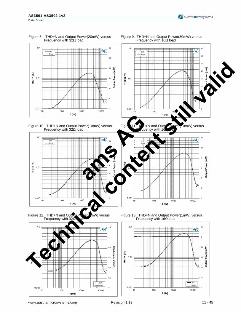
Figure 8. THD+N and Output Power(20mW) versus Frequency with 32Ω load
Figure 9. THD+N and Output Power(30mW) versus Frequency with 16Ω load
0
5
10
15
20
25
30
0,001
0,01
0,1
10 100 1000 10000
Ou
tpu
t P
ow
er
[mW
]
TH
D+
N [
%]
f [Hz]
Left
Right
0
5
10
15
20
25
30
35
40
0,001
0,01
0,1
10 100 1000 10000
Ou
tpu
t P
ow
er
[mW
]
TH
D+
N [
%]
f [Hz]
Left
Right
Figure 10. THD+N and Output Power(10mW) versus Frequency with 32Ω load
Figure 11. THD+N and Output Power(10mW) versus Frequency with 16Ω load
0
2
4
6
8
10
12
14
0,001
0,01
0,1
10 100 1000 10000
Ou
tpu
t P
ow
er
[mW
]
TH
D+
N [
%]
f [Hz]
Left
Right
0
2
4
6
8
10
12
0,001
0,01
0,1
10 100 1000 10000
Ou
tpu
t P
ow
er
[mW
]
TH
D+
N [
%]
f [Hz]
Left
Right
Figure 12. THD+N and Output Power(1mW) versus Frequency with 32Ω load
Figure 13. THD+N and Output Power(1mW) versus Frequency with 16Ω load
0
0,2
0,4
0,6
0,8
1
1,2
0,001
0,01
0,1
10 100 1000 10000
Ou
tpu
t P
ow
er
[mW
]
TH
D+
N [
%]
f [Hz]
Left
Right
0
0,2
0,4
0,6
0,8
1
1,2
0,001
0,01
0,1
10 100 1000 10000
Ou
tpu
t P
ow
er
[mW
]
TH
D+
N [
%]
f [Hz]
Left
Right
ams A
G
Technica
l conten
t still
valid

www.austriamicrosystems.com Revision 1.13 12 - 45
AS3501 AS3502 1v2Data Sheet
Figure 14. Typical Performance Data, FF configuration with an over the ear headset
Figure 15. Typical Performance Data, Feedback configuration with an on ear headset
-30
-25
-20
-15
-10
-5
0
5
10
10 100 1000 10000
AN
C P
erf
orm
ance
[d
B]
f [Hz]
Feed Forward Topology - Over the Ear Headset
-30
-25
-20
-15
-10
-5
0
5
10
10 100 1000 10000
AN
C P
erf
orm
an
ce [d
B]
f [Hz]
Feedback Topology - On Ear Headset
ams A
G
Technica
l conten
t still
valid

www.austriamicrosystems.com Revision 1.13 13 - 45
AS3501 AS3502 1v2Data Sheet
8 Detailed Description8.1 Audio Line Input
8.1.1 GeneralThe chip features one line input. The blocks can work in mono differential or in stereo single ended mode.
In addition to the 12.5-25kΩ input impedance, LineIn has a termination resistor of 10kΩ which is also effective during MUTE to charge eventually given input capacitors.
8.1.2 Gain StageThe Line In gain stage is designed to have 63 gain steps of 0.75dB with a max gain of 0dB plus MUTE.
In default, the gain will be ramped up from MUTE to 0dB during startup. There is a possibility to make the playback vol-ume user controlled by the VOL pin with an ADC converted VOL voltage or UP/DN buttons.
In monitor mode the gain stage can be set to an fixed default attenuation level for reducing the loudness of the music.
Figure 16. Line Inputs
8.1.3 Parameter
VBAT=1.5V, TA= 25oC, unless otherwise mentioned
Table 4. Line Input Parameter
Symbol Parameter Condition Min Typ Max Unit
VLIN Input Signal Level 0.6*VBAT VBAT VPEAK
RLIN Input Impedance
0dB gain (12.5k // 10k) 5.6 kΩ
-46.5dB gain (25k // 10k) 7.2 kΩ
MUTE 10 kΩ
∆RLIN Input Impedance Tolerance ±30 %
CLIN Input Capacitance 5 pF
ALIN Programmable Gain -46.5 +0 dB
Gain Steps discrete logarithmic gain steps 0.75 dB
Gain Step Accuracy 0.5 dB
ALINMUTE Mute Attenuation 100 dB
ams A
G
Technica
l conten
t still
valid

www.austriamicrosystems.com Revision 1.13 14 - 45
AS3501 AS3502 1v2Data Sheet
8.2 Microphone Input
8.2.1 GeneralThe AFE offers two microphone inputs and one low noise microphone voltage supply (microphone bias). The inputs can be switched to single ended or differential mode.
Figure 17. Microphone Input
8.2.2 Gain Stage & LimiterThe Mic Gain Stage has programmable Gain within -6dB…+41.625dB in 128 steps of 0.375dB.
As soft-start function is implemented for an automatic gain ramping implemented with steps of 4ms to fade in the audio at the end of the start-up sequence.
A limiter automatically attenuates high input signals. The AGC has 127 steps with 0.375dB with a dynamic range of the full gain stage.
In monitor mode the gain stage can be set to an fixed (normally higher) gain level or be controlled by the VOL pin.
8.2.3 SupplyThe MICS charge pump is providing a proper microphone supply voltage for the AAA supply. Since AAA batteries are operating down to 1.0V, the direct battery voltage cannot be used for mic-supply. There are 2 modes.
The first mode SWITCH-MODE for 1.8V supply is to have just a switch from VBAT to MICS. With this switch, the micro-phone current is switched off in idle mode.
The second mode CHAREGPUMP_MODE for AAA batteries is the real charge pump mode, in this mode a positive voltage is generated of about 2* VBAT.
It is also possible to switch off the microphone supply if not needed (e.g. playback without ANC)
∆ALIN Gain Ramp Rate
Poti Mode, Tinit=100ms 20ms/stepButton Mode, Tinit=400ms 80
Monitor Mode 8
VATTACK Limiter Activation Level HPL/R start of neg. clipping VPEAK
VDECAY Limiter Release Level HPL/R VNEG +0.3 VPEAK
tATTACK Limiter Attack Time 4 µs
tDECAY Limiter Decay Time 8 ms
Table 4. Line Input Parameter (Continued)
Symbol Parameter Condition Min Typ Max Unit
ams A
G
Technica
l conten
t still
valid

www.austriamicrosystems.com Revision 1.13 15 - 45
AS3501 AS3502 1v2Data Sheet
8.2.4 Parameter
VBAT=1.5V, TA= 25oC unless otherwise mentioned
Table 5. Microphone Input Parameter
Symbol Parameter Condition Min Typ Max Unit
VMICIN0 Input Signal Level AMIC = 30dB 20 mVP
VMICIN1 AMIC = 36dB 10 mVP
VMICIN2 AMIC = 42dB 5 mVP
RMICIN Input Impedance MICP to AGND 7.5 kΩ
∆MICIN Input Impedance Tolerance -7+33 %
CMICIN Input Capacitance 5 pF
AMIC Programmable Gain -6 +41.6 dB
Gain Steps discrete logarithmic gain steps 0.375 dB
Gain Step Precision 0.15 dB
∆AMIC Gain Ramp Rate Tinit=64ms 4 ms/step
VATTACK Limiter Activation LevelVPEAK related to VBAT or VNEG
0.67 1
VDECAY Limiter Release Level 0.4 1
AMICLIMIT Limiter Gain Overdrive 127 @ 0.375dB 41.625 dB
tATTACK Limiter Attack Time 5 µs/step
tDECAY-DEBLimiter Decay Debouncing
Time 64 ms
tDECAY Limiter Decay Time 4 ms/step
VMICS Microphone Supply Voltage VBAT*2-240mV V
IMICSMINMin. Microphone Supply
Current
VBAT=+1.0VVNEG=-0.7VMICS=+1.75V
650 uA
ROUT_CP CP Output Resistance 1300 Ω
ams A
G
Technica
l conten
t still
valid

www.austriamicrosystems.com Revision 1.13 16 - 45
AS3501 AS3502 1v2Data Sheet
8.3 Headphone Output
8.3.1 GeneralThe headphone output is a true ground output using VNEG as negative supply, designed to provide the audio signal with 2x12mW @ 16Ω−64Ω, which are typical values for headphones. It is also capable to operate in bridged mode for higher impedance (e.g. 300Ω) headphone. In this mode the left output is carrying the inverted signal of the right output.
Figure 18. Headphone Output
8.3.2 Input MultiplexerThe signal from the line-input gain stage gets summed at the input of the headphone stage with the microphone gain stage output, the first filter opamp output or the second filter opamp output. The microphone gain stage output is used per default. It is also possible to playback without ANC by only using the line-input gain stage with no other signal on the multiplexer.
For the monitor mode the setting of this input multiplexer can be changed to an other source, normally to the micro-phone.
8.3.3 No-Pop FunctionThe No-Pop startup of the headphone stage takes 60ms to 120ms dependent on the supply voltage.
8.3.4 No-Clip FunctionThe headphone output stage gets monitored by comparator stages which detect if the output signal starts to clip.
This signal is used to reduce the LineIn gain to avoid distortion of the output signal. A hystereses avoids jumping between 2 gain steps for a signal with constant amplitude.
8.3.5 Over-current protectionThe over-current protection has a threshold of 150-200mA and a debouncing time of 8us. The stage is forced to OFF mode in an over-current situation. After this the headphone stage tries to power up again every 8ms as long as the over-current situation still exists or the stage is turned off manually.
ams A
G
Technica
l conten
t still
valid

www.austriamicrosystems.com Revision 1.13 17 - 45
AS3501 AS3502 1v2Data Sheet
8.3.6 Parameter
VBAT=1.5V, TA= 25oC, unless otherwise mentioned
8.4 Operational Amplifier
8.4.1 GeneralWhile AS3501 offers only one operational amplifiers for feed-forward ANC AS3502 feature an additional second oper-ational amplifier stage to perform feed-back ANC or any other additional needed filtering.
Both operational amplifiers stages can be activated and used individually. While OP1 stage is always configured as inverting amplifier OP2 stage can be also switched to a non-inverting mode with an adjustable gain of 0..+10.5dB.
Figure 19. Operational Amplifiers
8.4.2 Parameter
VBAT=1.5V, TA= 25oC, unless otherwise mentioned
Table 6. Headphone Output Parameter
Symbol Parameter Condition Min Typ Max Unit
RL_HP Load Impedance stereo mode 16 Ω
CL_HP Load Capacitance stereo mode 100 pF
PHP Nominal Output Power RL=16Ω-64Ω 12 mW
PSRRHPPower Supply Rejection
Ratio 200Hz-20kHz, 720mVpp, RL=16Ω 90 dB
Table 7. Headphone Output Parameter
Symbol Parameter Condition Min Typ Max Unit
RL_OP Load Impedance single ended 1 kΩ
CL_OP Load Capacitance single ended 100 pF
GBWOP Gain Band Width 4.3 MHz
VOS_OP Offset Voltage 6 mV
VEIN_HP Equivalent Input Noise 200Hz-20kHz 2.6 uV
ams A
G
Technica
l conten
t still
valid

www.austriamicrosystems.com Revision 1.13 18 - 45
AS3501 AS3502 1v2Data Sheet
8.5 SYSTEM
8.5.1 GeneralThe system block handles the power up and power down sequencing. As well as the mode switching.
8.5.2 Power Up/Down ConditionsThe chip powers up when one of the following condition is true:
The chip automatically shuts off if one of the following conditions arises:
8.5.3 Start-up SequenceThe start-up sequence depends on the used mode.
In stand-alone mode the sequence runs automatically, in I2C mode the sequence runs till a defined state and waits then for an I2C command. Either the automatic sequence is started by setting the CONT_PWRUP bit in addition to the PWR_HOLD bit. If only the PWR_HOLD is set all enable bits for headphone, microphone, etc have to be set manually.
Figure 20. Stand-Alone Mode Start-Up Sequence
Table 8. Power UP Conditions
# Source Description
1 MODE pin In stand-alone mode, MODE pin has to be driven high to turn on the device
2 I2C start In I2C mode, a I2C start condition turns on the device
Table 9. Power DOWN Conditions
# Source Description
1 MODE pin Power down by driving MODE pin to low
2 SERIF Power down by SERIF writing 0h to register 20h bit <0>
3 Low Battery Power down if VBAT is lower than the supervisor off-threshold
4 VNEG CP OVC Power down if VNEG is higher than the VNEG off-threshold
ams A
G
Technica
l conten
t still
valid

www.austriamicrosystems.com Revision 1.13 19 - 45
AS3501 AS3502 1v2Data Sheet
Figure 21. I2C Mode Start-Up Sequence
8.5.4 Mode SwitchingWhen the chip in stand-alone mode (no I2C control) the mode can be switched with different levels on the MODE pin.
In I2C mode the monitor mode can be activated be setting the corresponding bit in the system register.
8.5.5 Status IndicationAS3501and AS3502 feature a on-status information via the current output pin ILED. The current can be controlled in 3 steps and be switched off, by setting the PWM accordingly (0%, 25%, 50% and 100% duty cycle of a 50kHz PWM sig-nal).
If LOW_BAT (typ. 0.9V) is active, ILED switches to blinking with 1Hz, 50% duty cycle and 50% current setting.
Table 10. Operation Modes
MODE MODE pin Description
OFF LOW (VNEG) Chip is turned off
ANC HIGH (VBAT) Chip is turned on and active noise cancellation is active
MONITOR TRI-STATE(VBAT/2)
Chip is turned on and monitor mode is activeIn Monitor mode a different (normally higher) microphone preamplifier gain can be chosen to get an amplification of the surrounding noise. This volume can be either fixed or be controlled by the VOL input.To get rid of the low pass filtering needed for the noise cancellation, the headphone input multiplexer can be set to a different (normally to MIC) source.In addition the LineIn gain can be lowered to reduce the loudness of the music currently played back.
ams A
G
Technica
l conten
t still
valid

www.austriamicrosystems.com Revision 1.13 20 - 45
AS3501 AS3502 1v2Data Sheet
8.6 VNEG Charge Pump
8.6.1 GeneralThe VNEG charge pump uses one external 1uF capacitor to generate a negative supply voltage out of the battery input voltage to supply all audio related blocks. This allows a true-ground headphone output with no more need of external dc-decoupling capacitors.
8.6.2 Parameter
VBAT=1.5V, TA= 25oC, unless otherwise mentioned
8.7 OTP Memory & Internal Registers
8.7.1 GeneralThe OTP memory consists of OTP register and the OTP fuses.The OTP register can be written as often as wanted but will lose the content on power off. The OTP fuses are intended to store basic chip configurations as well as the micro-phone gain settings to optimize the ANC performance and get rid of sensitivity variations of different microphones. Burning the fuses can only be once and is a permanent change, which means the fuses keep the content even if the chip is powered down.
When the chip is controlled by a microcontroller via I2C, the OTP memory don’t has to be used.
8.7.2 Register & OTP Memory configurationThe following graphics is showing the principal register interaction.
Figure 22. Register Access
Registers 0x8, 0x9, 0xA, 0xB, 0xC and 0x21 have only effect when the corresponding “REG_ON” bit is set, otherwise the chip operates with the OTP Register settings which are loaded from the OTP fuses at every start-up.
Table 11. Headphone Output Parameter
Symbol Parameter Condition Min Typ Max Unit
VIN input voltage VBAT 1.0 1.5 1.8 V
VOUT output voltage VNEG -0.7 -1.5 -1.8 V
CEXT external flying capacitor 1 uF
ams A
G
Technica
l conten
t still
valid

www.austriamicrosystems.com Revision 1.13 21 - 45
AS3501 AS3502 1v2Data Sheet
All registers settings can be changed several times, but will loose the content on power off. When using the I2C mode the chip configuration has to be loaded from the microcontroller after every start-up. In stand alone mode the OTP fuses have to be programmed for a permanent change of the chip configuration.
A single OTP cell can be programmed only once. Per default, the cell is “0”; a programmed cell will contain a “1”. While it is not possible to reset a programmed bit from “1” to “0”, multiple OTP writes are possible, but only additional unprogrammed “0”-bits can be programmed to “1”.
Independent of the OTP programming, it is possible to overwrite the OTP register temporarily with an OTP write command at any time. This setting will be cleared and overwritten with the hard programmed OTP settings at each power-up sequence or by a LOAD operation.
The OTP memory can be accessed in the following ways:
LOAD Operation:
The LOAD operation reads the OTP fuses and loads the contents into the OTP register. A LOAD operation is automatically executed after each power-on-reset.
WRITE Operation:
The WRITE operation allows a temporary modification of the OTP register. It does not program the OTP. This operation can be invoked multiple times and will remain set while the chip is supplied with power and while the OTP register is not modified with another WRITE or LOAD operation.
READ Operation:
The READ operation reads the contents of the OTP register, for example to verify a WRITE command or to read the OTP memory after a LOAD command.
BURN Operation:
The BURN operation programs the contents of the OTP register permanently into the OTP fuses. Don’t use old or nearly empty batteries for burning the fuses.
Attention: If you once burn the OTP_LOCK bit no further programming, e.g. setting additional “0” to “1”, of the OTP can be done.
For production the OTP_LOCK bit must be set to avoid an unwanted change of the OTP content during the lifetime of the product.
8.7.3 OTP fuse burningIn most stand alone applications the I2C pins are not accessible. Burning the fuses can be done by switching the line inputs into a special mode to access the chip by I2C over the line input connections. This allows trimming of the micro-phone gain with no openings in the final housing and so no influence to the acoustic of the headset.
This mode is called “Application Trim” mode, or short “APT”. (Patent Pending)
During the application trim mode LINR has to provide the clock, while LINL has to provide the data for the I2C commu-nication.
Please note that the OTP register cannot be accessed directly but have to be enabled before a read or write access. This is independent whether you access the OTP register via the normal I2C pins or in application trim mode via LINL and LINR. Please refer to the detailed register description to get more information on how the registers can be accessed.
To achieve a proper burning of the fuses, the negative supply has to be buffered by applying an external negative sup-ply during burning. This voltage can also be applied to the LINL terminal. An internal switch is connecting LINL and VNEG during the fuse burning. LINR has to provide the clock for burning the fuses.
The below flow chart shows the principle steps of the OTP burning process. The application trim mode can only be entered once. There is no possibility to stop the sequence, exit and re-enter the application trim mode to make e.g. the verification in a second step. The OTP bring sequence has to be done as shown in the flow chart.
A more detailed description of the individual steps is available in an application note.
ams A
G
Technica
l conten
t still
valid

www.austriamicrosystems.com Revision 1.13 22 - 45
AS3501 AS3502 1v2Data Sheet
Figure 23. OTP Burning Process
ams A
G
Technica
l conten
t still
valid

www.austriamicrosystems.com Revision 1.13 23 - 45
AS3501 AS3502 1v2Data Sheet
8.8 2-Wire-Serial Control Interface
8.8.1 GeneralThere is an I2C slave block implemented to have access to 64 byte of setting information.
The I2C address is: Adr_Group8 - audio processors
8Eh_write
8Fh_read
8.8.2 Protocol
Figure 24. Byte Write
Figure 25. Page Write
Byte Write and Page Write formats are used to write data to the slave.
The transmission begins with the START condition, which is generated by the master when the bus is in IDLE state (the bus is free). The device-write address is followed by the word address. After the word address any number of data bytes can be sent to the slave. The word address is incremented internally, in order to write subsequent data bytes on subsequent address locations.
Table 12. 2-Wire Serial Symbol Definition
Symbol Definition RW Note
S Start condition after stop R 1 bit
Sr Repeated start R 1 bit
DW Device address for write R 1000 1110b (8Eh)
DR Device address for read R 1000 1111b (8Fh)
WA Word address R 8 bit
A Acknowledge W 1 bit
N No Acknowledge R 1 bit
reg_data Register data/write R 8 bit
data (n) Register data/read W 8 bit
P Stop condition R 1 bit
WA++ Increment word address internally R during acknowledge
AS3501 AS3502 (=slave) receives data
AS3501 AS3502 (=slave) transmits dataams A
G
Technica
l conten
t still
valid

www.austriamicrosystems.com Revision 1.13 24 - 45
AS3501 AS3502 1v2Data Sheet
For reading data from the slave device, the master has to change the transfer direction. This can be done either with a repeated START condition followed by the device-read address, or simply with a new transmission START followed by the device-read address, when the bus is in IDLE state. The device-read address is always followed by the 1st register byte transmitted from the slave. In Read Mode any number of subsequent register bytes can be read from the slave. The word address is incremented internally.
Figure 26. Random Read
Random Read and Sequential Read are combined formats. The repeated START condition is used to change the direction after the data transfer from the master.
The word address transfer is initiated with a START condition issued by the master while the bus is idle. The START condition is followed by the device-write address and the word address.
In order to change the data direction a repeated START condition is issued on the 1st SCL pulse after the acknowl-edge bit of the word address transfer. After the reception of the device-read address, the slave becomes the transmit-ter. In this state the slave transmits register data located by the previous received word address vector. The master responds to the data byte with a not-acknowledge, and issues a STOP condition on the bus.
Figure 27. Sequential Read
Sequential Read is the extended form of Random Read, as more than one register-data bytes are transferred subse-quently. In difference to the Random Read, for a sequential read the transferred register-data bytes are responded by an acknowledge from the master. The number of data bytes transferred in one sequence is unlimited (consider the behavior of the word-address counter). To terminate the transmission the master has to send a not-acknowledge fol-lowing the last data byte and generate the STOP condition subsequently.
Figure 28. Current Address Read
To keep the access time as small as possible, this format allows a read access without the word address transfer in advance to the data transfer. The bus is idle and the master issues a START condition followed by the Device-Read address. Analogous to Random Read, a single byte transfer is terminated with a not-acknowledge after the 1st register byte. Analogous to Sequential Read an unlimited number of data bytes can be transferred, where the data bytes has to be responded with an acknowledge from the master. For termination of the transmission the master sends a not-acknowledge following the last data byte and a subsequent STOP condition.
ams A
G
Technica
l conten
t still
valid

www.austriamicrosystems.com Revision 1.13 25 - 45
AS3501 AS3502 1v2Data Sheet
8.8.3 Parameter
Figure 29. 2-Wire Serial Timing
VBAT >=1.4V, Tamb=25ºC; unless otherwise specified
Table 13. 2-Wire Serial Parameter
Symbol Parameter Condition Min Typ Max Unit
VCSLCSCL, CSDA Low Input
Level (max 30%VBAT) 0 - 0.42 V
VCSHCSCL, CSDA High Input
Level CSCL, CSDA (min 70%VBAT) 0.98 - V
HYST CSCL, CSDA Input Hysteresis 200 450 800 mV
VOL CSDA Low Output Level at 3mA - - 0.4 V
Tsp Spike insensitivity 50 100 - ns
TH Clock high time max. 400kHz clock speed 500 ns
TL Clock low time max. 400kHz clock speed 500 ns
TSUCSDA has to change Tsetup before
rising edge of CSCL 250 - - ns
THDNo hold time needed for CSDA relative
to rising edge of CSCL 0 - - ns
TS CSDA H hold time relative to CSDA edge for start/stop/rep_start 200 - - ns
TPDCSDA prop delay relative to low going
edge of CSCL 50 ns
ams A
G
Technica
l conten
t still
valid
ww
w.austriam
icrosystems.com
Revision 1.13
26 - 45
AS
35
01
AS
35
02
1v2
Da
ta S
he
et - R
eg
iste
r De
sc
riptio
n
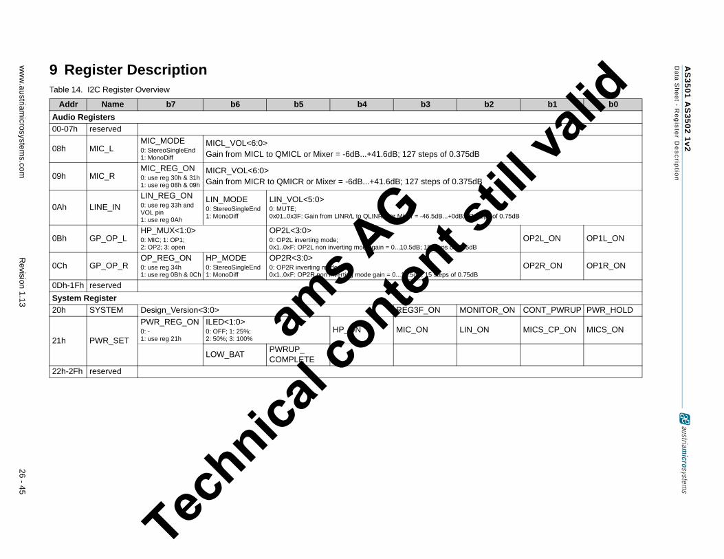
9 Register DescriptionTable 14. I2C Register Overview
Addr Name b7 b6 b5 b4 b3 b2 b1 b0
Audio Registers00-07h reserved
08h MIC_LMIC_MODE0: StereoSingleEnd1: MonoDiff
MICL_VOL<6:0>Gain from MICL to QMICL or Mixer = -6dB...+41.6dB; 127 steps of 0.375dB
09h MIC_RMIC_REG_ON0: use reg 30h & 31h1: use reg 08h & 09h
MICR_VOL<6:0>Gain from MICR to QMICR or Mixer = -6dB...+41.6dB; 127 steps of 0.375dB
0Ah LINE_INLIN_REG_ON0: use reg 33h and VOL pin1: use reg 0Ah
LIN_MODE0: StereoSingleEnd1: MonoDiff
LIN_VOL<5:0>0: MUTE;0x01..0x3F: Gain from LINR/L to QLINR/L or Mixer = -46.5dB...+0dB; 63 steps of 0.75dB
0Bh GP_OP_LHP_MUX<1:0>0: MIC; 1: OP1;2: OP2; 3: open
OP2L<3:0>0: OP2L inverting mode;0x1..0xF: OP2L non inverting mode gain = 0...10.5dB; 15 steps of 0.75dB
OP2L_ON OP1L_ON
0Ch GP_OP_ROP_REG_ON0: use reg 34h1: use reg 0Bh & 0Ch
HP_MODE0: StereoSingleEnd1: MonoDiff
OP2R<3:0>0: OP2R inverting mode;0x1..0xF: OP2R non inverting mode gain = 0...10.5dB; 15 steps of 0.75dB
OP2R_ON OP1R_ON
0Dh-1Fh reserved
System Register20h SYSTEM Design_Version<3:0> REG3F_ON MONITOR_ON CONT_PWRUP PWR_HOLD
21h PWR_SET
PWR_REG_ON0: -1: use reg 21h
ILED<1:0>0: OFF; 1: 25%;2: 50%; 3: 100%
HP_ON MIC_ON LIN_ON MICS_CP_ON MICS_ON
LOW_BATPWRUP_COMPLETE
22h-2Fh reserved
ams A
G
Technica
l conten
t still
valid

ww
w.austriam
icrosystems.com
Revision 1.13
27 - 45
AS
35
01
AS
35
02
1v2
Da
ta S
he
et - R
eg
iste
r De
sc
riptio
n
OTP Register
30h ANC_L TEST_BIT_1MICL_VOL_OTP<6:0>Gain from MICL to QMICL or Mixer = -6dB...+41.6dB; 127 steps of 0.375dB
31h ANC_R TEST_BIT_2MICR_VOL_OTP<6:0>Gain from MICR to QMICR or Mixer = -6dB...+41.6dB; 127 steps of 0.375dB
32h MIC_MONMON_MODE0: fixed volume1: adj. volume
MIC_MON_OTP<6:0>Gain from MICl/R to QMICL/R or Mixer = -6dB...+41.6dB; 0.375dB steps, if MON_MODE is set to 0Gain from MICl/R to QMICL/R or Mixer = -6dB...+41.6dB; 0.375dB steps, adjustable by VOL pin if MON_MODE is set to 1
33h AUDIO_SET VOL_PIN_OFF
VOL_PIN_MODE0: potentiometer1: up/down button
LIN_MODE_OTP0: StereoSingleEnd1: MonoDiff
MIC_MODE_OTP0: StereoSingleEnd1: MonoDiff
HP_MODE_OTP0: StereoSingleEnd1: MonoDiff
LIN_MON_ATTEN<2:0>0: no attenuation;1..6: LIN_VOL<6:0> shift by -6dB...-36dB7: MUTE
34h GP_OPHP_MUX_OTP<1:0>0: MIC; 1: OP1;2: OP2; 3: -
OP2_OTP<3:0>0: OP2 inverting mode;0x1..0xF: OP2 non inverting mode gain = 0...10.5dB; 15 steps of 0.75dB
OP2_ON_OTPOP1_ON_OTP
35h OTP_SYSOTP_LOCK0: write reg 30h.. 35h1: lock reg 30h..35h
TEST_BIT_5MON_HP_MUX<1:0>0: MIC; 1: OP1;2: OP2; 3: -
ILED_OTP<1:0>0: OFF; 1: 25%;2: 50%; 3: 100%
MICS_CP_OFF I2C_MODE
36h-3Dh reserved
3Eh CONFIG_1 EXTBURNCLK
3Fh CONFIG_2 BURNSW TM_REG34-35 TM_REG30-33OTP_MODE<1:0>0: READ; 1: LOAD;2: WRITE; 3: BURN
Table 14. I2C Register Overview
Addr Name b7 b6 b5 b4 b3 b2 b1 b0
ams A
G
Technica
l conten
t still
valid
www.austriamicrosystems.com Revision 1.13 28 - 45
AS3501 AS3502 1v2Data Sheet
Table 15. MIC_L Register
Name Base Default
MIC_L 2-wire serial 00h
Offset: 08hLeft Microphone Input Register
Configures the gain for the left microphone input and defines the microphone operation mode. This register is reset at POR.
Bit Bit Name Default Access Bit Description
7 MIC_MODE 0 R/W Selects the microphone input mode0: single ended stereo mode1: mono differential mode
6:0 MICL_VOL<6:0> 000 0000 R/W Volume settings for left microphone input, adjustable in 127 steps of 0.375dB00 0000: MUTE00 0001: -5.625dB gain00 0010: -5.25 dB gain..11 1110: 41.250dB gain11 1111: 41.625 dB gain
Table 16. MIC_R Register
Name Base Default
MIC_R 2-wire serial 00h
Offset: 09hRight Microphone Input Register
Configures the gain for the right microphone input and enables register 08h & 09h. This register is reset at POR.
Bit Bit Name Default Access Bit Description
7 MIC_REG_ON 0 R/W Defines which registers are used for the microphone settings.0:settings of register 30h and 31h are used1: settings of register 08h and 09h are used
6:0 MICR_VOL<6:0> 000 0000 R/W Volume settings for right microphone input, adjustable in 127 steps of 0.375dB00 0000: MUTE00 0001: -5.625dB gain00 0010: -5.25 dB gain..11 1110: 41.250dB gain11 1111: 41.625 dB gain
ams A
G
Technica
l conten
t still
valid

www.austriamicrosystems.com Revision 1.13 29 - 45
AS3501 AS3502 1v2Data Sheet
Table 17. LINE_IN Register
Name Base Default
LINE_IN 2-wire serial 00h
Offset: 0AhLine Input Register
Configures the attenuation for the line input, defines the line input operation mode and enables register 0Ah. This register is reset at POR.
Bit Bit Name Default Access Bit Description
7 LIN_REG_ON 0 R/W Defines which source is used for the line input settings.0: settings of register 33h and VOL pin are used1: register 0Ah is used
6 LIN_MODE 0 R/W Selects the line input mode0: single ended stereo mode1: mono differential mode
5:0 LIN_VOL<5:0> 00 0000 R/W Volume settings for line input, adjustable in 63 steps of 0.75dB00 0000: MUTE00 0001:-46.5dB gain00 0010:-45.75dB dain..11 1110:-0.75dB gain11 1111:.0 dB gain
Table 18. GP_OP_L Register
Name Base Default
GP_OP_L 2-wire serial 00h
Offset: 0BhLeft General Purpose Operational Amplifier Register
Enables the left opamp stages, defines opamp 2 mode and gain and sets the HP input multiplexer. This register is reset at POR.
Bit Bit Name Default Access Bit Description
7:6 HP_MUX<1:0> 00 R/W Multiplexes the analog audio signal to HP amp00: MIC: selects QMICL/R output01: OP1: selects QOP1L/R outputs10:OP2: selects QOP2L/R output11: open: no signal mixed together with the line input signal
5:2 OP2L<3:0> 0000 R/W Mode and volume settings for left OP2, adjustable in 15 steps of 0.75dB0000: OP2L in inverting mode0001: 0 dB gain, OP2L in non inverting mode0001: 0.75 dB gain, non inverting..,1110: 9.75dB gain, non inverting1111:.10.5 dB gain, non inverting
1 OP2L_ON 0 R/W Enables left OP 20: left OP2 is switched off1: left OP2 is enabled
0 OP1L_ON 0 R/W Enables left OP 10: left OP1 is switched off1: left OP1 is enabled
ams A
G
Technica
l conten
t still
valid
www.austriamicrosystems.com Revision 1.13 30 - 45
AS3501 AS3502 1v2Data Sheet
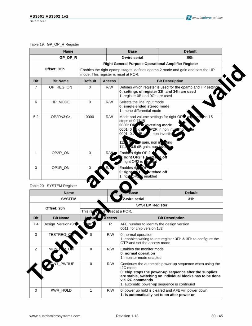
Table 19. GP_OP_R Register
Name Base Default
GP_OP_R 2-wire serial 00h
Offset: 0ChRight General Purpose Operational Amplifier Register
Enables the right opamp stages, defines opamp 2 mode and gain and sets the HP mode. This register is reset at POR.
Bit Bit Name Default Access Bit Description
7 OP_REG_ON 0 R/W Defines which register is used for the opamp and HP settings.0: settings of register 33h and 34h are used1: register 0B and 0Ch are used
6 HP_MODE 0 R/W Selects the line input mode0: single ended stereo mode1: mono differential mode
5:2 OP2R<3:0> 0000 R/W Mode and volume settings for right OP2, adjustable in 15 steps of 0.75dB0000: OP2R in inverting mode0001: 0 dB gain, OP2R in non inverting mode0001: 0.75 dB gain, non inverting..,1110: 9.75dB gain, non inverting1111:.10.5 dB gain, non inverting
1 OP2R_ON 0 R/W Enables right OP 20: right OP2 is switched off1: right OP2 is enabled
0 OP1R_ON 0 R/W Enables right OP 10: right OP1 is switched off1: right OP1 is enabled
Table 20. SYSTEM Register
Name Base Default
SYSTEM 2-wire serial 31h
Offset: 20hSYSTEM Register
This register is reset at a POR.
Bit Bit Name Default Access Bit Description
7:4 Design_Version<3:0> 0011 R AFE number to identify the design version0011: for chip version 1v2
3 TESTREG_ON 0 R/W 0: normal operation1: enables writing to test register 3Eh & 3Fh to configure the OTP and set the access mode.
2 MONITOR_ON 0 R/W Enables the monitor mode0: normal operation1: monitor mode enabled
1 CONT_PWRUP 0 R/W Continues the automatic power-up sequence when using the I2C mode0: chip stops the power-up sequence after the supplies are stable, switching on individual blocks has to be done via I2C commands1: automatic power-up sequence is continued
0 PWR_HOLD 1 R/W 0: power up hold is cleared and AFE will power down1: is automatically set to on after power on
ams A
G
Technica
l conten
t still
valid

www.austriamicrosystems.com Revision 1.13 31 - 45
AS3501 AS3502 1v2Data Sheet
Table 21. PWR_SET Register
Name Base Default
PWR_SET 2-wire serial0x11 1111b (stand alone mode)
0x00 0000b (I2C mode)
Offset: 21h
Power Setting Register
Please be aware that writing to this register will enable/disable the corresponding blocks, while reading gets the actual status. It is not possible to read back e.g ILED settings. This register is reset at POR.
Bit Bit Name Default Access Bit Description
7 PWR_REG_ON 0 R/W Defines which register is used for the power settings.0: all blocks stay on as defined in the start-up sequence1: register 21h is used
6:5 ILED<1:0> 00 W Sets the current sunk into ILED00: current sink switched OFF01: 25%10: 50%11: 100%
6 LOW_BAT x R VBAT supervisor status0: VBAT is above brown out level1: BVDD has reached brown out level
5 PWRUP_COMPLETE x R Power-Up sequencer status0: power-up sequence incomplete1: power-up sequence completed
4 HP_ON 0 W 0: switches HP stage off1: switches HP stage on
x R 0: HP stage not powered1: normal operation
3 MIC_ON 0 W 0: switches microphone stage off1: switches microphone stage on
x R 0: microphone stage not powered1: normal operation
2 LIN_ON 0 W 0: switches line input stage off1: switches line input stage on
x R 0: line input stage not powered1: normal operation
1 MICS_CP_ON 0 W 0: switches microphone supply charge pump off1: switches microphone supply charge pump on
x R 0: microphone supply charge pump not powered1: normal operation
0 MICS_ON 0 W 0: switches microphone supply off1: switches microphone supply on
x R 0: microphone supply not enabled1: normal operation
ams A
G
Technica
l conten
t still
valid
www.austriamicrosystems.com Revision 1.13 32 - 45
AS3501 AS3502 1v2Data Sheet
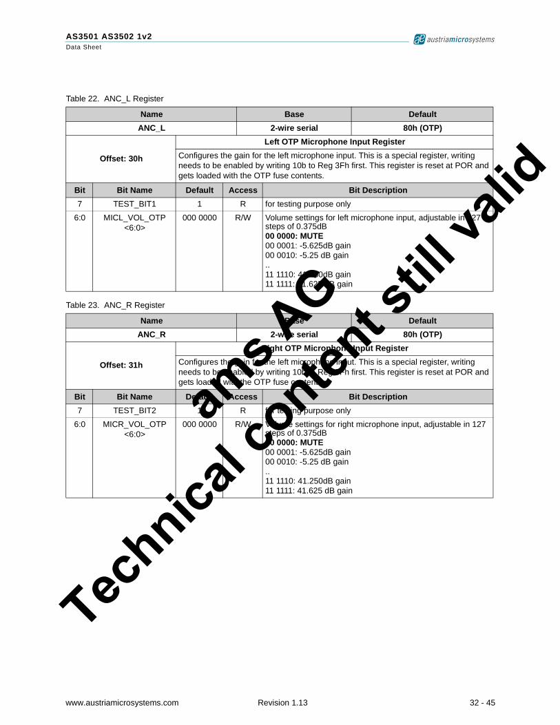
Table 22. ANC_L Register
Name Base Default
ANC_L 2-wire serial 80h (OTP)
Offset: 30h
Left OTP Microphone Input Register
Configures the gain for the left microphone input. This is a special register, writing needs to be enabled by writing 10b to Reg 3Fh first. This register is reset at POR and gets loaded with the OTP fuse contents.
Bit Bit Name Default Access Bit Description
7 TEST_BIT1 1 R for testing purpose only
6:0 MICL_VOL_OTP<6:0>
000 0000 R/W Volume settings for left microphone input, adjustable in 127 steps of 0.375dB00 0000: MUTE00 0001: -5.625dB gain00 0010: -5.25 dB gain..11 1110: 41.250dB gain11 1111: 41.625 dB gain
Table 23. ANC_R Register
Name Base Default
ANC_R 2-wire serial 80h (OTP)
Offset: 31h
Right OTP Microphone Input Register
Configures the gain for the left microphone input. This is a special register, writing needs to be enabled by writing 10b to Reg 3Fh first. This register is reset at POR and gets loaded with the OTP fuse contents.
Bit Bit Name Default Access Bit Description
7 TEST_BIT2 1 R for testing purpose only
6:0 MICR_VOL_OTP<6:0>
000 0000 R/W Volume settings for right microphone input, adjustable in 127 steps of 0.375dB00 0000: MUTE00 0001: -5.625dB gain00 0010: -5.25 dB gain..11 1110: 41.250dB gain11 1111: 41.625 dB gain
ams A
G
Technica
l conten
t still
valid

www.austriamicrosystems.com Revision 1.13 33 - 45
AS3501 AS3502 1v2Data Sheet
Table 24. MIC_MON Register
Name Base Default
MIC_MON 2-wire serial 00h (OTP)
Offset: 32h
OPT Microphone Monitor Mode Register
Configures the gain for the microphone input in monitor mode. This is a special register, writing needs to be enabled by writing 10b to Reg 3Fh first. This register is reset at POR and gets loaded with the OTP fuse contents.
Bit Bit Name Default Access Bit Description
7 MON_MODE 0 R/W 0: monitor mode is working with fixed microphone gain1: monitor mode uses adjustable gain via the VOL pin
6:0 MIC_MON_OTP<6:0>
000 0000 R/W Volume settings for microphone input during monitor mode, adjustable in 127 steps of 0.375dB. If MON_MODE bit is set to 1 the gain can be further adjusted via the VOL pin.00 0000: MUTE00 0001: -5.625dB gain00 0010: -5.25 dB gain..11 1110: 41.250dB gain11 1111: 41.625 dB gain
Table 25. AUDIO_SET Register
Name Base Default
AUDIO_SET 2-wire serial 00h (OTP)
Offset: 33h
OPT Audio Setting Register
Configures the audio settings. This is a special register, writing needs to be enabled by writing 10b to Reg 3Fh first. This register is reset at POR and gets loaded with the OTP fuse contents.
Bit Bit Name Default Access Bit Description
7 VOL_PIN_OFF 0 R/W 0: VOL pin is enabled1: line in volume settings can only be done via I2C. VOL_PIN_MODE has to be set to 1 in this mode.
6 VOL_PIN_MODE 0 R/W 0: VOL pin is in potentiometer mode1: VOL pin is in up/down button mode
5 LIN_MODE_OTP 0 R/W 0: line input stage opeating in single ended mode1: line input operating in mono balanced
4 MIC_MODE_OTP 0 R/W 0: microphone input stage opeating in single ended mode1: normal operating in mono balanced
3 HP_MODE_OTP 0 R/W 0: headphone stage opeating in single ended mode1: normal operating in mono balanced
2:0 LIN_MON_ATTEN<6:0>
000 R/W Volume settings for line input during monitor mode, adjustable in 7 steps of 6dB and mute. 000: 0dB gain001: -6dB gain..110: -36dB gain111: MUTE
ams A
G
Technica
l conten
t still
valid

www.austriamicrosystems.com Revision 1.13 34 - 45
AS3501 AS3502 1v2Data Sheet
Table 26. GP_OP Register
Name Base Default
GP_OP 2-wire serial 00h (OTP)
Offset: 34h
OTP General Purpose Operational Amplifier Register
Enables the opamp stages, defines opamp 2 mode and gain and sets the HP input multiplexer. This is a special register, writing needs to be enabled by writing 10b to Reg 3Fh first. This register is reset at POR and gets loaded with the OTP fuse contents.
Bit Bit Name Default Access Bit Description
7:6 HP_MUX_OTP<1:0> 00 R/W Multiplexes the analog audio signal to HP amp00: MIC: selects QMICL/R output01:OP1: selects QOP1L/R outputs10:OP2: selects QOP2L/R output11: open: no signal mixed together with the line input signal
5:2 OP2_OTP<3:0> 0000 R/W Mode and volume settings for OP2, adjustable in 15 steps of 0.75dB0000: OP2L in inverting mode0001: 0 dB gain, OP2L in non inverting mode0001: 0.75 dB gain, non inverting..,1110: 9.75dB gain, non inverting1111:.10.5 dB gain, non inverting
1 OP2_ON 0 R/W 0: OP2 is switched off1: left OP2 is enabled
0 OPL_ON 0 R/W 0: OP1 is switched off1: OP1 is enabled
Table 27. OTP_SYS Register
Name Base Default
OTP_SYS 2-wire serial 40h (OTP)
Offset: 35h
OTP System Settings Register
Defines several system settings for OTP operation. This is a special register, writing needs to be enabled by writing 10b to Reg 3Fh first. This register is reset at POR and gets loaded with the OTP fuse contents.
Bit Bit Name Default Access Bit Description
7 OTP_LOCK 0 R/W 0: additional bits can be fused inside the OTP1: OTP fusing gets locked, no more changes can be done
6 TEST_BIT5 1 R for testing purpose only
5:4 MON_HP_MUX<1:0>
00 R/W Multiplexes the analog audio signal to HP amp in monitor mode00: MIC: selects QMICL/R output01: OP1: selects QOP1L/R outputs10:OP2: selects QOP2L/R output11: open: no signal mixed together with the line input signal
3:2 ILED_OTP<1:0> 00 W Sets the current sunk into ILED00: current sink switched OFF01: 25%10: 50%11: 100%
ams A
G
Technica
l conten
t still
valid

www.austriamicrosystems.com Revision 1.13 35 - 45
AS3501 AS3502 1v2Data Sheet
1 MICS_CP_OFF 0 R/W 0: MICS charge pump is enabled1: MICS charge pump is switched off
0 I2C 0 R/W 0: I2C and stand alone mode start-up possible1: chip starts-up in I2C mode only
Table 28. CONFIG_1 Register
Name Base Default
CONFIG_1 2-wire serial 00h
Offset: 3Eh
OTP Configuration Register
Controls the clock configuration. This is a special register, writing needs to be enabled by writing 9h to Reg 20h first. This register is reset at POR and gets loaded with the OTP fuse contents.
Bit Bit Name Default Access Bit Description
7:4 - 0000 n/a
3 EXTBURNCLK 0 n/a 0: ext. clock for OTP burning disabled1: ext. clock for OTP burning enabled
2:0 - 000 n/a
Table 29. CONFIG_2 Register
Name Base Default
CONFIG_2 2-wire serial 00h
Offset: 3Fh
OTP Access Configuration Register
Controls the OTP access. This is a special register, writing needs to be enabled by writing 9h to Reg 20h first. This register is reset at POR and gets loaded with the OTP fuse contents.
Bit Bit Name Default Access Bit Description
7:5 - 000 n/a
4 BURNSW 0 n/a 0: BURN switch from LINL to VNEG is disabled1: BURN switch from LINL to VNEG is enabled
3 TM_REG34-35 0 n/a 0: test mode for Register 34h-35h disabled1: test mode for Register 34h-35h enabled
2 TM_REG30-33 0 n/a 0: test mode for Register 30h-33h disabled1: test mode for Register 30h-33h enabled
1:0 OTP_MODE<1:0> 00 R/W Controls the OTP access00: READ01: LOAD10: WRITE11: BURN
Table 27. OTP_SYS Register
Name Base Default
OTP_SYS 2-wire serial 40h (OTP)
Offset: 35h
OTP System Settings Register
Defines several system settings for OTP operation. This is a special register, writing needs to be enabled by writing 10b to Reg 3Fh first. This register is reset at POR and gets loaded with the OTP fuse contents.
Bit Bit Name Default Access Bit Description
ams A
G
Technica
l conten
t still
valid
www.austriamicrosystems.com Revision 1.13 36 - 45
AS3501 AS3502 1v2Data Sheet
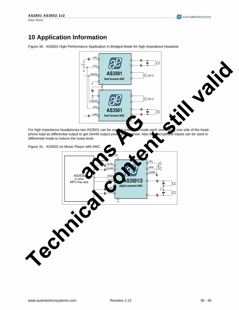
10 Application InformationFigure 30. AS3501 High Performance Application in Bridged Mode for high impedance headsets
For high impedance headphones two AS3501 can be used in a bridged mode each one driving one side of the head-phone load as differential output to get 24mW output power per channel. Also the microphone inputs can be used in differential mode to reduce the noise level.
Figure 31. AS3502 on Music Player with ANC
ams A
G
Technica
l conten
t still
valid

www.austriamicrosystems.com Revision 1.13 37 - 45
AS3501 AS3502 1v2Data Sheet
Figure 32. AS3501 feed-forward application example
11
22
33
44
DD
CC
BB
AA
C6 1uF
C12
2.2
uF
R14
2k2
C13
2.2
uF
R13
2k2
P1A
50k
C3
10u
C10
10u
Vp
os
Vp
os
Vn
eg
Vn
eg
C15
22uF
MIC
S
MIC
S
Volu
me C
ontr
ol
43 2
1
U3
AA
A B
atte
rie
Battery
Socket
MIC
S
R19
150R
R20
150R
L3
GN
D1
R2
U2
Lin
e In
put
HE
AD
PH
ON
E
for
open loop n
ois
e c
ancela
tion
Vp
os
R18
10k
R17
10k
Monitor
Butt
on
23
1
ON
/OF
F B
ypas
s sl
ider
23
1
23
1
Altern
ative V
olu
me C
ontr
ol
LE
D
VC
C
R1
470R
C1
10uF
+1
-2
J? Rig
ht S
pea
ker
+1
-2
J? Lef
t S
pea
ker
R?
R?
C?
R?
R?
C?
Val
ues
dep
. on
hea
dphone
char
acte
rist
ics,
als
o
oth
er topolo
gie
s poss
ible
Val
ues
dep
. on
hea
dphone
char
acte
rist
ics,
als
o
oth
er topolo
gie
s poss
ible
C8
22nF
C7
22nF
GN
DG
ND
Mic
LP
F c
ap d
ep.
on h
eadphone
char
acte
rist
ics
Vn
eg
+1
-2
J? AN
C M
IC L
eft
+1
-2
J? AN
C M
IC L
eft
AS
3501
QM
ICL
1
AG
ND
2
LIN
L3
LIN
R4
VO
L_
CS
DA
5
MO
DE
_C
SC
L6
MICL7
ILED8
MICS9
MICR10
QMICR11
IOP1R12Q
OP
1R
13
VS
S1
4
HP
L1
5
HP
R1
6
HV
DD
17
VB
AT
18
CPP19
GND20
CPN21
VNEG22
QOP1L23
IOP1L24
U1
AS
3501
must NOT be connected to GND or AGND!CAUTION: Exposed pad must be connected to VNEG or left unconnected. Exposed pad
ams A
G
Technica
l conten
t still
valid

www.austriamicrosystems.com Revision 1.13 38 - 45
AS3501 AS3502 1v2Data Sheet
Figure 33. AS3502 feed-back application example
11
22
33
44
55
66
77
88
DD
CC
BB
AA
C61u
C122.2u
R14
2k2
C132.2u
R13
2k2
R15
R9
R16
C16R
10
C17R11
C18
R12
C14
C11
P1A
50k
R6
R5R4
R3
R2
R1
C5
C4
C2
C9
C1
C3
10
u
C10
10
u
D1
LE
D
Vp
os
Vp
os
Vn
eg
Vn
eg
C15
22
uF
MIC
S
MIC
S
Vp
os
Pow
er
Le
d
Volu
me C
ontr
ol
43 2
1
U3
AA
A B
atte
rie
Batt
ery
Socket
MIC
S
R19
150R
R20
15
0R
L3
GN
D1
R2
U2
Lin
e In
put
HE
AD
PH
ON
E
for
clo
se
d lo
op n
ois
e c
ancela
tion
C8
C7
Vp
os
R18
10
k
R17
10
k
Mo
nito
r B
utt
on
23
1
ON
/OF
F B
ypas
s sl
ider
23
1
23
1
LINE
+ -5 4 32
LINE
+ -5 4 32
Alte
rnative V
olu
me C
on
trol
LP
F a
nd N
OT
CH
-Fil
ter
to a
vo
id o
scil
lati
on b
y ac
ust
ic (
Hea
dphone-
Sp
eaker
<=
> M
ic)
LP
F a
nd
NO
TC
H-F
ilte
r to
av
oid
osc
illa
tion b
y ac
ust
ic
(Hea
dpho
ne-
Spea
ker
<=
> M
ic)
Mic
Sup
ply
re
sist
ors
dep
end
on
Mic
Sp
ec
R25
470R
C20
10
uF
Mic
LP
F c
ap d
ep.
on
Hea
dp
hon
e C
har
acte
rist
ics
Mic
LP
F
cap
dep
. o
n
Hea
dph
one
Char
acte
ris
tics
QL
INL
2
QM
ICL
3
AG
ND
4
LIN
L5
LIN
R6
MO
DE
/CS
CL
8
VO
L/C
SD
A7
MICL9
MICS11
ILED10
MICR12
QMICR13
QLINR14
IOP1R15
QOP1R16
IOP
2R
17
QO
P2
R1
8
VS
S1
9
HP
L2
0
HV
SS
21
HP
R2
2
HV
DD
23
VB
AT
24
CPP26
GND27
CPN28
VNEG29
QOP2L30
IOP2L31
QOP1L32
IOP
1L
1
NC25
AS
3502
U?
AS
3502
must NOT be connected to GND or AGND!CAUTION: Exposed pad must be connected to VNEG or left unconnected. Exposed pad
ams A
G
Technica
l conten
t still
valid

www.austriamicrosystems.com Revision 1.13 39 - 45
AS3501 AS3502 1v2Data Sheet
Figure 34. AS3501 Li-Ion battery bridged mode differential feed forward application example
11
22
33
44
DD
CC
BB
AA
L3
GN
D1
R2
U1
GN
DG
ND
GN
DG
NDG
ND
Vp
os
Vp
os
L1
4.7
uH
BU
1
BU
2
Vn
eg
Vn
eg
L
Vp
os
GN
D
Vp
os
LE
D
Vp
os
GN
DG
ND
Vp
os
Vn
eg
Vn
eg
L
R5
150
R2
2k2
R1
2k2
R3
2k2
R6
150
R4
2k2
C2
1uF
C1
1uF
C8
2.2
uF
C7
2.2
uF
C6
2.2
uF
C5
2.2
uF
C9
C10
C11
470n
C14
470n
C15
470n
C16
470n
C17
10u
C18
10u
C19
2.2
uF
C3
10u
C4
10u
+1
-2
s1
+1
-2
s2
GN
D
GN
D
VIN
EN
SW
Vo
ut
AS
1324-1
5
C20
4.7
uF
R7
220R
GN
D
Mic
LP
F c
ap d
ep.
on H
eadphone
Char
acte
rist
ics
Mic
LP
F c
ap d
ep.
on H
eadphone
Char
acte
rist
ics
C21
2.2
uF
C22
4.7
uF
R8
220R
GN
D
C12
10u
GN
DG
ND
C13
10u
Vn
eg
AS
3501
QM
ICL
1
AG
ND
2
LIN
L3
LIN
R4
VO
L_
CS
DA
5
MO
DE
_C
SC
L6
MICL7
ILED8
MICS9
MICR10
QMICR11
IOP1R12Q
OP
1R
13
VS
S1
4
HP
L1
5
HP
R1
6
HV
DD
17
VB
AT
18
CPP19
GND20
CPN21
VNEG22
QOP1L23
IOP1L24
U?
AS
3501
AS
3501
QM
ICL
1
AG
ND
2
LIN
L3
LIN
R4
VO
L_
CS
DA
5
MO
DE
_C
SC
L6
MICL7
ILED8
MICS9
MICR10
QMICR11
IOP1R12Q
OP
1R
13
VS
S1
4
HP
L1
5
HP
R1
6
HV
DD
17
VB
AT
18
CPP19
GND20
CPN21
VNEG22
QOP1L23
IOP1L24
U?
AS
3501
+1
-2
M2
AN
C M
ic
+1
-2
M1
AN
C M
ic
must N
OT be conn
ected to GND or AGND!
CA
UT
ION
: Exposed
pad
must b
e conn
ected to VNEG or left un
conn
ected. Exposed
pad
ams A
G
Technica
l conten
t still
valid

www.austriamicrosystems.com Revision 1.13 40 - 45
AS3501 AS3502 1v2Data Sheet
11 Package Drawings and MarkingsFigure 35. QFN Marking
Table 30. Package Code YYWWXZZ
YY WW X ZZ
last two digits of the year manufacturing week plant identifier free choice / traceability code
ams A
G
Technica
l conten
t still
valid
www.austriamicrosystems.com Revision 1.13 41 - 45
AS3501 AS3502 1v2Data Sheet
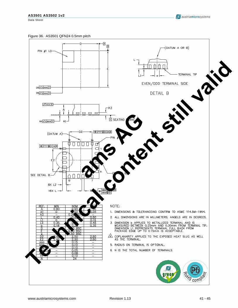
Figure 36. AS3501 QFN24 0.5mm pitch
ams A
G
Technica
l conten
t still
valid
www.austriamicrosystems.com Revision 1.13 42 - 45
AS3501 AS3502 1v2Data Sheet
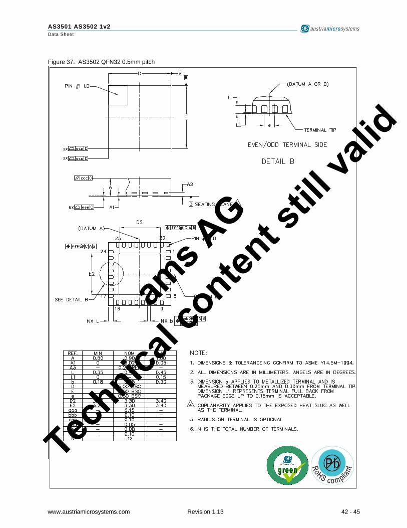
Figure 37. AS3502 QFN32 0.5mm pitch
ams A
G
Technica
l conten
t still
valid

www.austriamicrosystems.com Revision 1.13 43 - 45
AS3501 AS3502 1v2Data Sheet
12 Ordering Information
The devices are available as the standard products shown in Table 31.
Note: All products are RoHS compliant and austriamicrosystems green.
Buy our products or get free samples online at ICdirect: http://www.austriamicrosystems.com/ICdirect
For further information and requests, please contact us mailto:[email protected]
or find your local distributor at http://www.austriamicrosystems.com/distributor
Table 31. Ordering Information
Ordering Code Description Delivery Form Package
AS3501-EQFPLow Power Ambient Noise-Cancelling Speaker Driver
Tape & Reeldry pack
QFN 24 [4.0x4.0x0.85mm] 0.5mm pitch
AS3502-EQFPLow Power Ambient Noise-Cancelling Speaker Driver
Tape & Reeldry pack
QFN 32 [5.0x5.0x0.85mm] 0.5mm pitch
ams A
G
Technica
l conten
t still
valid

www.austriamicrosystems.com Revision 1.13 44 - 45
AS3501 AS3502 1v2Data Sheet
Revision History
Note: Typos may not be explicitly mentioned under revision history.
Table 32. Revision History
Revision Date Owner Description
1.0 18.5.2009 pkm official release
1.01 5.6.2009 pkm updated application schematics
1.02 15.7.2009 pkm typo correction
1.1 19.1.2009 pkm updated pin and pinout description
1.11 03.8.2010 hgt updated solder profile, power up sequences and block diagrams
1.12 09.6.2011 hgt updated order information and electrical characteristics
1.13 06.07.2011 hgtupdated package information, operating conditions, absolute maximum ratings and order information
ams A
G
Technica
l conten
t still
valid

www.austriamicrosystems.com Revision 1.13 45 - 45
AS3501 AS3502 1v2Data Sheet
Copyrights
Copyright © 1997-2009, austriamicrosystems AG, Schloss Premstaetten, 8141 Unterpremstaetten, Austria-Europe. Trademarks Registered ®. All rights reserved. The material herein may not be reproduced, adapted, merged, trans-lated, stored, or used without the prior written consent of the copyright owner.
All products and companies mentioned are trademarks or registered trademarks of their respective companies.
Disclaimer
Devices sold by austriamicrosystems AG are covered by the warranty and patent indemnification provisions appearing in its Term of Sale. austriamicrosystems AG makes no warranty, express, statutory, implied, or by description regarding the information set forth herein or regarding the freedom of the described devices from patent infringement. austriami-crosystems AG reserves the right to change specifications and prices at any time and without notice. Therefore, prior to designing this product into a system, it is necessary to check with austriamicrosystems AG for current information. This product is intended for use in normal commercial applications. Applications requiring extended temperature range, unusual environmental requirements, or high reliability applications, such as military, medical life-support or life-sustaining equipment are specifically not recommended without additional processing by austriamicrosystems AG for each application. For shipments of less than 100 parts the manufacturing flow might show deviations from the standard production flow, such as test flow or test location.
The information furnished here by austriamicrosystems AG is believed to be correct and accurate. However, austriamicrosystems AG shall not be liable to recipient or any third party for any damages, including but not limited to personal injury, property damage, loss of profits, loss of use, interruption of business or indirect, special, incidental or consequential damages, of any kind, in connection with or arising out of the furnishing, performance or use of the tech-nical data herein. No obligation or liability to recipient or any third party shall arise or flow out of austriamicrosystems AG rendering of technical or other services.
Contact Information
Headquartersaustriamicrosystems AGA-8141 Schloss Premstaetten, Austria
Tel: +43 (0) 3136 500 0Fax: +43 (0) 3136 525 01
For Sales Offices, Distributors and Representatives, please visit:
http://www.austriamicrosystems.com/contact
ams A
G
Technica
l conten
t still
valid