artificial neural networks for rf and microwave design ...qjz/ann_tutorial/paper-s4-33.pdf · tool...
TRANSCRIPT
1
Abstract -- Neural network computational modules have recently gained recognition as an unconventional and useful tool for RF and microwave modeling and design. Neural networks can be trained to learn the behavior of passive/active components/circuits. A trained neural network can be used for high-level design, providing fast and accurate answers to the task it has learned. Neural networks are attractive alternatives to conventional methods such as numerical modeling methods which could be computationally expensive, or analytical methods which could be difficult-to-obtain for new devices, or empirical modeling solutions whose range and accuracy may be limited. This tutorial describes fundamental concepts in this emerging area aimed at teaching RF/microwave engineers what neural networks are, why they are useful, when they can be used and how to use them. Neural network structures and their training methods are described from RF/microwave designer’s perspective. EM-based training for passive component models and physics-based training for active device models are illustrated. Circuit design and yield optimization using passive/active neural models are also presented. A multimedia slide presentation along with narrative audio clips is included in the electronic version of this article. A hyperlink to the NeuroModeler demonstration software is provided to allow readers practice neural network based design concepts. Index Terms -- CAD, design automation, modeling, neural networks, simulation, optimization
TABLE OF CONTENTS I. INTRODUCTION II. NEURAL NETWORK STRUCTURES A. Basic Components B. Concept of a Neural Network Model Qi-Jun Zhang and Vijay K. Devabhaktuni are with the Department of Electronics, Carleton University, Ottawa, Ontario, Canada, K1S 5B6. Kuldip C. Gupta is with the Department of Electrical and Computer Engineering, University of Colorado, Boulder, Colorado, USA, 80309-0425.
C. Neural Network versus Conventional Modeling D. Multilayer Perceptrons Neural Network D.1. Structure and Notation D.2. Anatomy of Neurons D.3. Feedforward Computation D.4. Important Features E. Network Size and Layers F. Other Neural Network Configurations III. NEURAL NETWORK MODEL DEVELOPMENT A. Problem Formulation and Data Processing A.1. ANN Inputs and Outputs A.2. Data Range and Sample Distribution A.3. Data Generation A.4. Data Organization A.5. Data Preprocessing B. Neural Network Training B.1. Weight Parameters Initialization B.2. Formulation of Training Process B.3. Error Derivative Computation B.4. More About Training B.5. Over-learning and Under-learning B.6. Quality Measures IV. COMPONENT MODELING USING NEURAL NETWORKS A. High-Speed Interconnect Network B. CPW Symmetric T-junction
Artificial Neural Networks for RF and Microwave Design: From Theory to Practice
Qi-Jun Zhang, Senior Member, IEEE, Kuldip C. Gupta, Fellow, IEEE,
Vijay K. Devabhaktuni, Student Member, IEEE
2
C. Transistor Modeling V. CIRCUIT OPTIMIZATION USING NEURAL NETWORK MODELS A. CPW Folded Double-Stub Filter B. Three-Stage MMIC Amplifier VI. CONCLUSIONS APPENDIX I: MULTI-MDEIA SLIDE PRESENTATION APPENDIX II: HYPERLINK TO NEUROMODELER SOFTWARE ACKNOWLEDGEMENTS REFERENCES
I. INTRODUCTION Neural networks, also called Artificial Neural Networks (ANN), are information processing systems with their design inspired by the studies of ability of human-brain to learn from observations and to generalize by abstraction [1]. The fact that neural networks can be trained to learn any arbitrary nonlinear input-output relationships from corresponding data has resulted in their use in a number of areas such as pattern recognition, speech processing, control, bio-medical engineering etc. Recently, ANNs have been applied to RF and microwave computer-aided design (CAD) problems as well. Neural networks are first trained to model the electrical behavior of passive and active components/circuits. These trained neural networks, often referred to as neural network models (or simply neural models), can then be used in high-level simulation and design, providing fast answers to the task they have learned [2][3]. Neural networks are efficient alternatives to conventional methods such as numerical modeling methods, which could be computationally expensive; or analytical methods, which could be difficult to obtain for new devices; or empirical models whose range and accuracy could be limited. Neural network techniques have been used for a wide variety of microwave applications such as embedded passives [4], transmission line components [5]-[7], vias [8], bends [9], CPW components [10], spiral inductors [11], FETs [12], amplifiers [13][14] etc. Neural networks have also been used in impedance matching [15], inverse modeling [16], measurements [17] and synthesis [18]. An increased number of RF/microwave engineers and researchers have started taking serious interest in this emerging technology. As such, this tutorial is prepared to meet the educational needs of the RF/microwave community. The subject of neural networks will be described from the point of view of RF/microwave engineers using microwave-oriented language and terminology. In Section II, neural network structural issues are introduced, and the popularly used multilayer perceptrons (MLP) neural network is described at length. Various steps involved in the development of neural
network models are described in Section III. Practical microwave examples illustrating the application of neural network techniques to component modeling and circuit optimization are presented in Sections IV and V respectively. Finally, Section VI contains the summary and conclusions. To further aid the readers in quickly grasping the ANN fundamentals and practical aspects, an electronic multimedia slide presentation of the tutorial and a hyperlink to NeuroModeler demonstration software [19] are included in the CD-ROM, accompanying this issue.
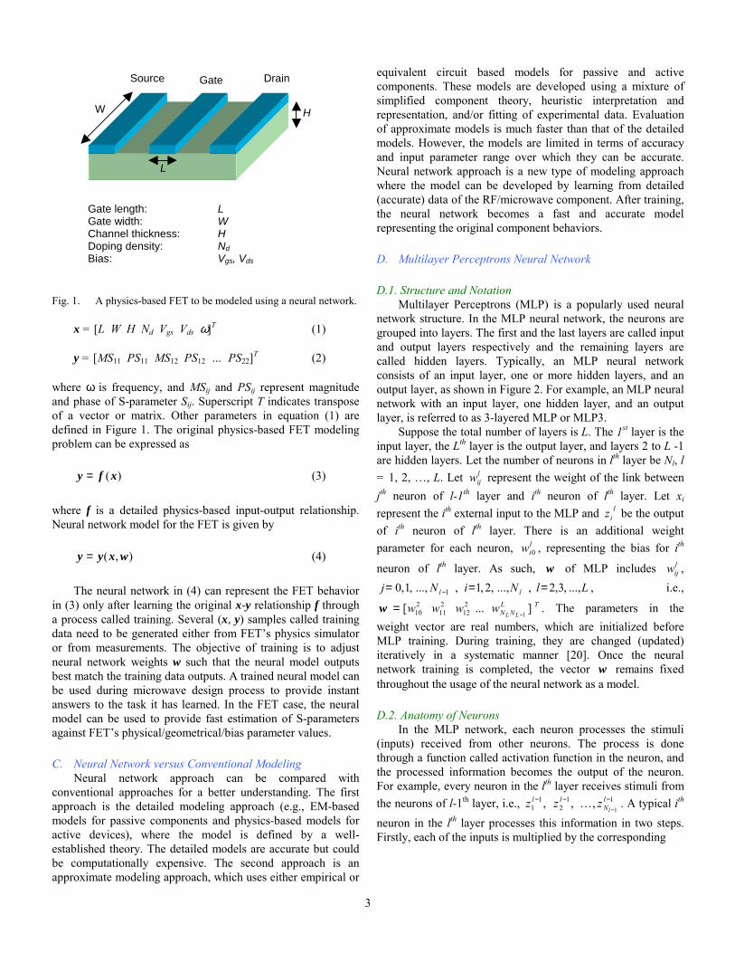
II. NEURAL NETWORK STRUCTURES We describe neural network structural issues to better understand what neural networks are and why they have the ability to represent RF and microwave component behaviors. We study neural networks from the external input-output point of view, and also from the internal neuron information processing point of view. The most popularly used neural network structure, i.e., the multilayer perceptron is described in detail. The effects of structural issues on modeling accuracy are discussed. A. Basic Components A typical neural network structure has two types of basic components, namely, the processing elements and the interconnections between them. The processing elements are called neurons and the connections between the neurons are known as links or synapses. Every link has a corresponding weight parameter associated with it. Each neuron receives stimulus from other neurons connected to it, processes the information, and produces an output. Neurons that receive stimuli from outside the network are called input neurons while neurons whose outputs are externally used are called output neurons. Neurons that receive stimuli from other neurons and whose outputs are stimuli for other neurons in the network are known as hidden neurons. Different neural network structures can be constructed by using different types of neurons and by connecting them differently. B. Concept of a Neural Network Model Let n and m represent the number of input and output neurons of a neural network. Let x be an n-vector containing the external inputs to the neural network, y be an m-vector containing the outputs from the output neurons, and w be a vector containing all the weight parameters representing various interconnections in the neural network. The definition of w , and the manner in which y is computed from x and w , determine the structure of the neural network. Consider a Field Effect Transistor (FET) shown in Figure 1. The physical/geometrical/bias parameters of the FET are variables and any change in the values of these parameters affects the electrical responses of the FET (e.g., small-signal S-parameters). Assume that there is a need to develop a neural model that can represent such input-output relationship. Inputs and outputs of the corresponding FET neural model are given by,
3
Fig. 1. A physics-based FET to be modeled using a neural network. x = [L W H Nd Vgs Vds ω]T (1)
y = [MS11 PS11 MS12 PS12 PS22]T (2)
where ω is frequency, and MSij and PSij represent magnitude and phase of S-parameter Sij. Superscript T indicates transpose of a vector or matrix. Other parameters in equation (1) are defined in Figure 1. The original physics-based FET modeling problem can be expressed as )(xfy = (3)
where f is a detailed physics-based input-output relationship. Neural network model for the FET is given by ),( wxyy = (4) The neural network in (4) can represent the FET behavior in (3) only after learning the original x-y relationship f through a process called training. Several (x, y) samples called training data need to be generated either from FETs physics simulator or from measurements. The objective of training is to adjust neural network weights w such that the neural model outputs best match the training data outputs. A trained neural model can be used during microwave design process to provide instant answers to the task it has learned. In the FET case, the neural model can be used to provide fast estimation of S-parameters against FETs physical/geometrical/bias parameter values. C. Neural Network versus Conventional Modeling Neural network approach can be compared with conventional approaches for a better understanding. The first approach is the detailed modeling approach (e.g., EM-based models for passive components and physics-based models for active devices), where the model is defined by a well-established theory. The detailed models are accurate but could be computationally expensive. The second approach is an approximate modeling approach, which uses either empirical or
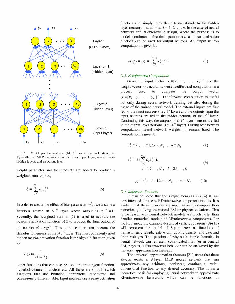
equivalent circuit based models for passive and active components. These models are developed using a mixture of simplified component theory, heuristic interpretation and representation, and/or fitting of experimental data. Evaluation of approximate models is much faster than that of the detailed models. However, the models are limited in terms of accuracy and input parameter range over which they can be accurate. Neural network approach is a new type of modeling approach where the model can be developed by learning from detailed (accurate) data of the RF/microwave component. After training, the neural network becomes a fast and accurate model representing the original component behaviors. D. Multilayer Perceptrons Neural Network D.1. Structure and Notation Multilayer Perceptrons (MLP) is a popularly used neural network structure. In the MLP neural network, the neurons are grouped into layers. The first and the last layers are called input and output layers respectively and the remaining layers are called hidden layers. Typically, an MLP neural network consists of an input layer, one or more hidden layers, and an output layer, as shown in Figure 2. For example, an MLP neural network with an input layer, one hidden layer, and an output layer, is referred to as 3-layered MLP or MLP3. Suppose the total number of layers is L. The 1st layer is the input layer, the Lth layer is the output layer, and layers 2 to L -1 are hidden layers. Let the number of neurons in lth layer be Nl, l = 1, 2, , L. Let l
ijw represent the weight of the link between jth neuron of l-1th layer and ith neuron of lth layer. Let xi represent the ith external input to the MLP and l
iz be the output of ith neuron of lth layer. There is an additional weight parameter for each neuron, l
iw 0 , representing the bias for ith
neuron of lth layer. As such, w of MLP includes lijw ,
LlNiNj ll ...,,3,2,...,,2,1,...,,1,0 1 === − , i.e., TL
NN LLwwww ]...[
1
212
211
210 −
=w . The parameters in the weight vector are real numbers, which are initialized before MLP training. During training, they are changed (updated) iteratively in a systematic manner [20]. Once the neural network training is completed, the vector w remains fixed throughout the usage of the neural network as a model. D.2. Anatomy of Neurons In the MLP network, each neuron processes the stimuli (inputs) received from other neurons. The process is done through a function called activation function in the neuron, and the processed information becomes the output of the neuron. For example, every neuron in the lth layer receives stimuli from the neurons of l-1th layer, i.e., 11
21
1 1,,, −−−
−
lN
lll
zzz . A typical ith neuron in the lth layer processes this information in two steps. Firstly, each of the inputs is multiplied by the corresponding
Gate length: L Gate width: W Channel thickness: H Doping density: Nd Bias: Vgs, Vds
Gate Drain
L
W H
Source
4
Fig. 2. Multilayer Perceptrons (MLP) neural network structure. Typically, an MLP network consists of an input layer, one or more hidden layers, and an output layer. weight parameter and the products are added to produce a weighted sum l
iγ , i.e.,
−
=
−=1
0
1lN
j
lj
lij
li zwγ (5)
In order to create the effect of bias parameter l
iw 0 , we assume a
fictitious neuron in l-1th layer whose output is 110 =−lz .
Secondly, the weighted sum in (5) is used to activate the neurons activation function )(⋅σ to produce the final output of
the neuron )( li
li γσz = . This output can, in turn, become the
stimulus to neurons in the l+1th layer. The most commonly used hidden neuron activation function is the sigmoid function given by
)1(
1)( γγσ −+=
e (6)
Other functions that can also be used are arc-tangent function, hyperbolic-tangent function etc. All these are smooth switch functions that are bounded, continuous, monotonic and continuously differentiable. Input neurons use a relay activation
function and simply relay the external stimuli to the hidden layer neurons, i.e., zi
1 = xi, i = 1, 2, , n. In the case of neural networks for RF/microwave design, where the purpose is to model continuous electrical parameters, a linear activation function can be used for output neurons. An output neuron computation is given by
−
=
−==1LN
0j)( 1L
jLij
Li
Li zwγγσ (7)
D.3. Feedforward Computation Given the input vector T
nxxx ][ 21 =x and the weight vector w , neural network feedforward computation is a process used to compute the output vector
Tmyyy ][ 21 =y . Feedforward computation is useful
not only during neural network training but also during the usage of the trained neural model. The external inputs are first fed to the input neurons (i.e., 1st layer) and the outputs from the input neurons are fed to the hidden neurons of the 2nd layer. Continuing this way, the outputs of L-1th layer neurons are fed to the output layer neurons (i.e., Lth layer). During feedforward computation, neural network weights w remain fixed. The computation is given by 11
1 ,,,2,1, NnNixz ii === (8)
LlNi
zwz
l
N
j
lj
lij
li
l
,,3,2,,,2,1
,)(1
0
1
==
= −
=
−σ (9)
LL
Lii NmNizy === ,,,2,1, (10)
D.4. Important Features It may be noted that the simple formulas in (8)-(10) are now intended for use as RF/microwave component models. It is evident that these formulas are much easier to compute than numerically solving theoretical EM or physics equations. This is the reason why neural network models are much faster than detailed numerical models of RF/microwave components. For the FET modeling example described earlier, equations (8)-(10) will represent the model of S-parameters as functions of transistor gate length, gate width, doping density, and gate and drain voltages. The question of why such simple formulas in neural network can represent complicated FET (or in general EM, physics, RF/microwave) behavior can be answered by the universal approximation theorem. The universal approximation theorem [21] states that there always exists a 3-layer MLP neural network that can approximate any arbitrary, nonlinear, continuous, multi-dimensional function to any desired accuracy. This forms a theoretical basis for employing neural networks to approximate RF/microwave behaviors, which can be functions of
1
x1 x2 x3 xn
y1 y2 ym
1 2 3 N1
1 2 3 N2
1 2 3 NL-1
2 NL
Layer L
Layer L - 1
Layer 2
Layer 1 (Input layer)
(Output layer)
(Hidden layer)
(Hidden layer)
5
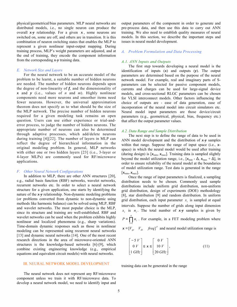
physical/geometrical/bias parameters. MLP neural networks are distributed models, i.e., no single neuron can produce the overall x-y relationship. For a given x , some neurons are switched on, some are off, and others are in transition. It is this combination of neuron switching states that enables the MLP to represent a given nonlinear input-output mapping. During training process, MLPs weight parameters are adjusted, and at the end of training, they encode the component information from the corresponding x-y training data. E. Network Size and Layers For the neural network to be an accurate model of the problem to be learnt, a suitable number of hidden neurons are needed. The number of hidden neurons depends upon the degree of non-linearity of f, and the dimensionality of x and y (i.e., values of n and m). Highly nonlinear components need more neurons and smoother items need fewer neurons. However, the universal approximation theorem does not specify as to what should be the size of the MLP network. The precise number of hidden neurons required for a given modeling task remains an open question. Users can use either experience or trial-and-error process, to judge the number of hidden neurons. The appropriate number of neurons can also be determined through adaptive processes, which add/delete neurons during training [4][22]. The number of layers in MLP can reflect the degree of hierarchical information in the original modeling problem. In general, MLP networks with either one or two hidden layers [23] (i.e., 3-layer or 4-layer MLPs) are commonly used for RF/microwave applications. F. Other Neural Network Configurations In addition to MLP, there are other ANN structures [20], e.g., radial basis function (RBF) networks, wavelet networks, recurrent networks etc. In order to select a neural network structure for a given application, one starts by identifying the nature of the x-y relationship. Non-dynamic modeling problems (or problems converted from dynamic to non-dynamic using methods like harmonic balance) can be solved using MLP, RBF and wavelet networks. The most popular choice is the MLP, since its structure and training are well-established. RBF and wavelet networks can be used when the problem exhibits highly nonlinear and localized phenomena (e.g., sharp variations). Time-domain dynamic responses such as those in nonlinear modeling can be represented using recurrent neural networks [13] and dynamic neural networks [14]. One of the most recent research directions in the area of microwave-oriented ANN structures is the knowledge-based networks [6]-[9], which combine existing engineering knowledge (e.g., empirical equations and equivalent circuit models) with neural networks.
III. NEURAL NETWORK MODEL DEVELOPMENT The neural network does not represent any RF/microwave
component unless we train it with RF/microwave data. To develop a neural network model, we need to identify input and
output parameters of the component in order to generate and pre-process data, and then use this data to carry out ANN training. We also need to establish quality measures of neural models. In this section, we describe the important steps and issues in neural model development. A. Problem Formulation and Data Processing A.1. ANN Inputs and Outputs The first step towards developing a neural model is the identification of inputs (x) and outputs (y). The output parameters are determined based on the purpose of the neural network model. For example, real and imaginary parts of S-parameters can be selected for passive component models, currents and charges can be used for large-signal device models, and cross-sectional RLGC parameters can be chosen for VLSI interconnect models. Other factors influencing the choice of outputs are - ease of data generation, ease of incorporation of the neural model into circuit simulators etc. Neural model input parameters are those device/circuit parameters (e.g., geometrical, physical, bias, frequency etc.) that affect the output parameter values. A.2. Data Range and Sample Distribution The next step is to define the range of data to be used in ANN model development and the distribution of x-y samples within that range. Suppose the range of input space (i.e., x-space) in which the neural model would be used after training (during design) is [xmin, xmax]. Training data is sampled slightly beyond the model utilization range, i.e., [xmin - ∆, xmax + ∆], in order to ensure reliability of the neural model at the boundaries of model utilization range. Test data is generated in the range [xmin, xmax]. Once the range of input parameters is finalized, a sampling distribution needs to be chosen. Commonly used sample distributions include uniform grid distribution, non-uniform grid distribution, design of experiments (DOE) methodology [8], star distribution [9] and random distribution. In uniform grid distribution, each input parameter ix is sampled at equal intervals. Suppose the number of grids along input dimension
ix is in . The total number of x-y samples is given by
∏=
=n
iinP
1. For example, in a FET modeling problem where
Tdsgs freqVV ][=x and neural model utilization range is
≤≤
−
GHzVV
GHzVV
20100
105
x , (11)
training data can be generated in the range

6
++≤≤
−
−−
220110
0
5.010
5.05x . (12)
In non-uniform grid distribution, each input parameter is sampled at unequal intervals. This is useful when the problem behavior is highly nonlinear in certain sub-regions of the x-space and dense sampling is needed in such sub-regions. Modeling DC characteristics (I-V curves) of a FET is a classic example for non-uniform grid distribution. Sample distributions based on DOE (e.g., 2n factorial experimental design, central composite experimental design) and star distribution are used in situations where training data generation is expensive. A.3. Data Generation In this step, x-y sample pairs are generated using either simulation software (e.g., 3D-EM simulations using Ansoft-HFSS [24]) or measurement setup (e.g., S-parameter measurements from a network analyzer). The generated data could be used for training the neural network and testing the resulting neural network model. In practice, both simulations and measurements could have small errors. While errors in simulation could be due to truncation/round-off or non-convergence, errors in measurement could be due to equipment limitations or tolerances. Considering this, we introduce a vector d to represent the outputs from simulation/measurement corresponding to an input x. Data generation is then defined as the use of simulation/measurement to obtain sample pairs (xk, dk), k = 1, 2, , P. The total number of samples P is chosen such that the developed neural model best represents the given problem f. A general guideline is to generate larger number of samples for a nonlinear high-dimensional problem and fewer samples for a relatively smooth low-dimensional problem. A.4. Data Organization The generated (x, d) sample pairs could be divided into three sets, namely, training data, validation data, and test data. Let rT , V , eT and D represent index sets of training data, validation data, test data and generated (available) data respectively. Training data is utilized to guide the training process, i.e., to update the neural network weight parameters during training. Validation data is used to monitor the quality of the neural network model during training and to determine stop criteria for the training process. Test data is used to independently examine the final quality of the trained neural model in terms of accuracy and generalization capability. Ideally, each of the data sets rT , V and eT should adequately represent the original component behavior,
)(xfy = . In practice, available data D can be split depending upon its quantity. When D is sufficiently large, it can be split into three mutually disjoint sets. When D is limited due to expensive simulation or measurement, it can be split into just two sets. One of the sets is used for training and validation ( VTr = ) and the other for testing ( eT ), or alternatively one of
the sets is used for training ( rT ) and the other for validation and testing ( eTV = ). A.5. Data Preprocessing Contrary to binary data (0s and 1s) in pattern recognition applications, the orders of magnitude of various input (x) and output (d) parameter values in microwave applications can be very different from one another. As such, a systematic preprocessing of training data called scaling is desirable for efficient neural network training. Let x, xmin and xmax represent a generic input element in the vectors x , minx and maxx of original (generated) data respectively. Let x~ , min
~x and max~x
represent a generic element in the vectors x~ , min~x and max
~x of scaled data, where ]~,~[ maxmin xx is the input parameter range after scaling. Linear scaling is given by
)~~(~~minmax
minmax
minmin xx
xxxxxx −−
−+= (13)
and corresponding de-scaling is given by
)(~~~~
minmaxminmax
minmin xx
xxxxxx −−
−+= (14)
Output parameters in training data, i.e., elements in d can also be scaled in a similar manner. Linear scaling of data can provide balance between different inputs (or outputs) whose values are different by orders of magnitude. Another scaling method is the logarithmic scaling [1], which can be applied to outputs with large variations in order to provide a balance between small and large values of the same output. In the training of knowledge-based networks, where knowledge neuron functions (e.g., Ohms law, Faradays law etc.) require preservation of physical meaning of the input parameters, training data is not scaled, i.e., xx ~= . At the end of this step, the scaled data is ready to be used for training. B. Neural Network Training B.1. Weight Parameters Initialization In this step, we prepare the neural network for training. The neural network weight parameters (w) are initialized so as to provide a good starting point for training (optimization). The widely used strategy for MLP weight initialization is to initialize the weights with small random values (e.g., in the range ]5.0,5.0[− ). Another method suggests that the range of random weights be inversely proportional to the square root of number of stimuli a neuron receives on average. To improve the convergence of training, one can use a variety of distributions (e.g., Gaussian distribution), and/or different ranges and different variances for the random number generators used in initializing the ANN weights [25].

7
B.2. Formulation of Training Process The most important step in neural model development is the neural network training. The training data consists of sample pairs, ,),( rkk Tk ∈dx , where kx and kd are n- and m-vectors representing the inputs and the desired outputs of the neural network. We define neural network training error as
∈ =
−=r
rTk
m
jjkkjT dy
2E
1
2),(1)( wxw (15)
where djk is the jth element of dk and ),( wxkjy is the jth neural network output for input kx . The purpose of neural network training, in basic terms, is to adjust w such that the error function )(w
rTE is minimized. Since )(w
rTE is a nonlinear function of the adjustable (i.e., trainable) weight parameters w , iterative algorithms are often used to explore the w-space efficiently. One begins with an initialized value of w and then iteratively updates it. Gradient-based iterative training techniques update w based on error
information )(wrTE and error derivative information
w∂∂
rTE.
The subsequent point in w -space denoted as nextw is determined by a step down from the current point noww along a direction vector h, i.e., hww ηnownext += . Here, hw η=∆ is called the weight update and η is a positive step size known as the learning rate. For example, backpropagation (BP) training algorithm [20] updates w along the negative direction of the
gradient of training error as w
ww∂
∂−= rTE
η .
B.3. Error Derivative Computation As mentioned earlier, gradient-based training techniques
require error derivative computation, i.e., w∂
∂rTE
. For the MLP
neural network, these derivatives are computed using a standard approach often referred to as error-backpropagation (EBP), which is described in this subsection. We define a per-sample error function Ek given by
2
1)),((
21
jkk
m
jjk dyE −=
=wx (16)
for kth data sample, rTk ∈ . Let L
iδ represent the error between ith neural network output and ith output in training data, i.e., ikki
Li dy −= ),( wxδ (17)
Starting from the output layer, this error can be backpropagated to the hidden layers as
2,3...,,2,1
),1(1
1
11
−−=
−
= +
=
+
+
LLl
zzw li
li
lji
N
j
lj
li
l
δδ (18)
where l
iδ represents local error at the ith neuron in lth layer. The derivative of the per-sample error in (16) w.r.t. a given neural network weight parameter l
ijw is given by
2,...,1,1 −==∂∂ − LLlzwE l
jlil
ij
k δ (19)
Finally, the derivative of the training error in (15) w.r.t. l
ijw can
be computed as ∈ ∂
∂=
∂
∂
r
r
Tklij
klij
T
wE
wE
. Using EBP, w∂
∂rTE
can be
systematically evaluated for the MLP neural network structure and can be provided to gradient-based training algorithms for the determination of weight update w∆ . B.4. More About Training Validation error VE and test error
eTE can be defined in a manner similar to (15) using the validation and test data sets V and eT . During ANN training, validation error is periodically evaluated and the training is terminated once a reasonable VE is reached. At the end of the training, the quality of the neural network model can be independently assessed by evaluating the test error
eTE . Neural network training algorithms commonly used in RF/microwave applications include gradient-based training techniques such as backpropagation, conjugate-gradient, quasi-Newton etc. Global optimization methods such as simulated annealing and genetic algorithms can be used for globally optimal solutions of neural network weights. But the training time required for global optimization methods is much longer than that for gradient based training techniques. Neural network training process can be categorized into sample-by-sample training and batch-mode training. In sample-by-sample training also called online training, w is updated each time a training sample ),( kk dx is presented to the network. In batch-mode training also known as offline training, w is updated after each epoch, where an epoch is defined as a stage of training process that involves presentation of all the training data (or samples) to the neural network once. In the RF/microwave case, batch-mode training is usually more effective. A flow-chart summarizing major steps in neural network training and testing is shown in Figure 3. B.5. Over-learning and Under-learning Ability of a neural network to estimate output ky accurately when presented with input kx never seen during

8
Fig. 3. Flow-chart demonstrating neural network training, neural model testing, and use of training, validation, and test data sets in ANN modeling approach. training (i.e., rTk ∉ ) is called generalization ability. The normalized training error is defined as
2
1
1
2
min,max,
),(1)(
−−
= ∈ =rr
rTk
m
j jj
jkkj
TT dd
dyPm
Ewx
w (20)
where jd min, and jd max, are the minimum and maximum values of the jth element of all kd , Dk ∈ , and
rTP is the number of
data samples in rT . The normalized validation error VE can be similarly defined. Good learning of a neural network is achieved when both
rTE and VE have small values (e.g., 0.50%) and are close to each other. The ANN exhibits over-learning, when it memorizes the training data but cannot generalize well (i.e.,
rTE is small but VE >>rTE ). Remedies
for over-learning are - deleting a certain number of hidden neurons or adding more samples to the training data. The neural network exhibits under-learning, when it has difficulties in learning the training data itself (i.e.,
rTE >> 0). Possible remedies are - adding more hidden neurons or perturbing the current solution w to escape from a local minimum of )(w
rTE , and then continuing training. B.6. Quality Measures The quality of a trained neural network model is evaluated with an independent set of data, i.e., eT . We define a relative error jkδ for jth output of neural model for kth test sample as
( )
ejj
jkkjjk Tkmj
dddy
∈=−
−= ,,,1,
,
min,max,
wxδ (21)
A quality measure based on qth-norm is then defined as
qqm
jjk
Tkq
e
M
1
1
=
=∈δ (22)
The average test error can be calculated using 1M as
eTPm
MErrorTestAverage 1= (23)
where eTP represents number of samples in test set eT . The
worst-case error among all test samples and all neural network model outputs can be calculated using )max(max
1 jk
m
jTekM δ
=∈∞ = (24)
Other statistical measures such as correlation coefficient and standard deviation can also be used.
IV. COMPONENT MODELING USING NEURAL NETWORKS
Component/device modeling is one of the most important areas of RF/microwave CAD. The efficiency of CAD tools depends largely on speed and accuracy of the component models. Development of neural network models for active devices, passive components and high-speed interconnects has already been demonstrated [6][8][26]. These neural models could be used in device level analysis and also in circuit/system level design [10][12]. In this section, neural network modeling examples are presented in each of the above-mentioned categories. A. High-Speed Interconnect Network
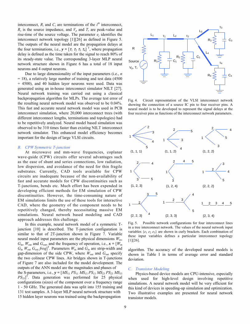
In this example, a neural network was trained to model signal propagation delays of a VLSI interconnect network in printed circuit boards (PCBs). The electrical equivalent circuit showing the interconnection of source IC pin to the receiver pins is shown in Figure 4. During PCB design, each individual interconnect network needs to be varied in terms of its interconnect lengths, receiver-pin load characteristics, source characteristics and network topology. To facilitate this, a neural network model of the interconnect configuration was developed [26].
The input variables in the model are x = [Li Ri Ci Rs Vp Tr ej]T, i = 1, 2, 3, 4 and j = 1, 2, 3. Here, Li is length of the ith
No
Evaluate validation
error
Perform feedforward
computation for all samples in
validation set
Assign random initial values for all
the weight parameters
Yes Select a neural
network structure, e.g., MLP STOP
TrainingEvaluate test error as an independent
quality measure for ANN model
quality
Perform feedforward
computation for all samples in test set
START
Desired accuracy
achieved?
Perform feedforward
computation for all samples in
training set
Compute derivatives of training error w.r.t. ANN
weights using EBP
Update neural network weight
parameters using a
gradient-based algorithm
Evaluate training
error
9
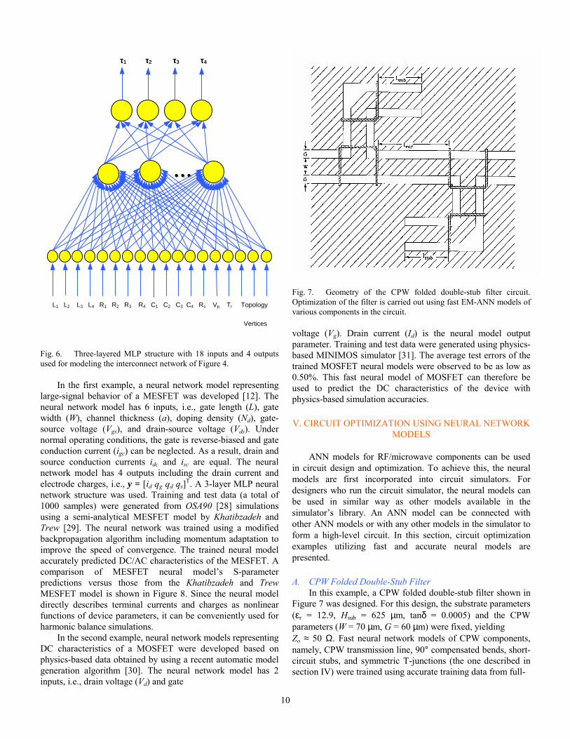
interconnect, Ri and Ci are terminations of the ith interconnect, Rs is the source impedance, and Vp and Tr are peak-value and rise-time of the source voltage. The parameter ej identifies the interconnect network topology [1][26] as defined in Figure 5. The outputs of the neural model are the propagation delays at the four terminations, i.e., y = [τ1 τ2 τ3 τ4] T, where propagation delay is defined as the time taken for the signal to reach 80% of its steady-state value. The corresponding 3-layer MLP neural network structure shown in Figure 6 has a total of 18 input neurons and 4 output neurons.
Due to large dimensionality of the input parameters (i.e., n = 18), a relatively large number of training and test data (4500 + 4500), and 40 hidden layer neurons were used. Data was generated using an in-house interconnect simulator NILT [27]. Neural network training was carried out using a classical backpropagation algorithm for MLPs. The average test error of the resulting neural network model was observed to be 0.04%. This fast and accurate neural network model was used in PCB interconnect simulation, where 20,000 interconnect trees (with different interconnect lengths, terminations and topologies) had to be repetitively analyzed. Neural model based simulation was observed to be 310 times faster than existing NILT interconnect network simulator. This enhanced model efficiency becomes important for the design of large VLSI circuits.
B. CPW Symmetric T-junction At microwave and mm-wave frequencies, coplanar wave-guide (CPW) circuits offer several advantages such as the ease of shunt and series connections, low radiation, low dispersion, and avoidance of the need for thin fragile substrates. Currently, CAD tools available for CPW circuits are inadequate because of the non-availability of fast and accurate models for CPW discontinuities such as T-junctions, bends etc. Much effort has been expended in developing efficient methods for EM simulation of CPW discontinuities. However, the time-consuming nature of EM simulations limits the use of these tools for interactive CAD, where the geometry of the component needs to be repetitively changed, thereby necessitating massive EM simulations. Neural network based modeling and CAD approach addresses this challenge. In this example, neural network model of a symmetric T-junction [10] is described. The T-junction configuration is similar to that of 2T-junction shown in Figure 7. Variable neural model input parameters are the physical dimensions Win, Gin, Wout and Gout, and the frequency of operation, i.e., x = [Win Gin Wout Gout freq]T. Parameters Win and Gin are strip-width and gap-dimension of the side CPW, where Wout and Gout specify the two colinear CPW lines. Air bridges shown in T-junctions of Figure 7 are also included for the model development. The outputs of the ANN model are the magnitudes and phases of the S-parameters, i.e., y = [MS11 PS11 MS13 PS13 MS23 PS23 MS33 PS33]T. Data generation was performed for 25 physical configurations (sizes) of the component over a frequency range 1 - 50 GHz. The generated data was split into 155 training and 131 test samples. A 3-layer MLP neural network structure with 15 hidden layer neurons was trained using the backpropagation
Fig. 4. Circuit representation of the VLSI interconnect network showing the connection of a source IC pin to four receiver pins. A neural model is to be developed to represent the signal delays at the four receiver pins as functions of the interconnect network parameters. Fig. 5. Possible network configurations for four interconnect lines in a tree interconnect network. The values of the neural network input variables e1 e2 e3 are shown in curly brackets. Each combination of these input variables defines a particular interconnect topology [1][26]. algorithm. The accuracy of the developed neural models is shown in Table I in terms of average error and standard deviation. C. Transistor Modeling Physics-based device models are CPU-intensive, especially when used for high-level design involving repetitive simulations. A neural network model will be very efficient for this kind of devices in speeding-up simulation and optimization. Two illustrative examples are presented for neural network transistor models.
Vp, Tr
Source
R4
R1
R2
L3L1 τ1 L2 τ2
R3 C3
τ3
C4
τ4
L4C2
C1
R
1
23
45
1, 1, 1
2
1 3
4
5
1, 1, 2
2
1
3
4
5
1, 2, 2
3
2
1
4
5
1, 2, 33
1
2 4 5
1, 2, 4
12
3
4
5
2, 2, 2
4
5
3 21
2, 3, 3
4 1 2 3 5
2, 3, 4
3
1 2
4
5
2, 2, 3
10
Fig. 6. Three-layered MLP structure with 18 inputs and 4 outputs used for modeling the interconnect network of Figure 4.
In the first example, a neural network model representing large-signal behavior of a MESFET was developed [12]. The neural network model has 6 inputs, i.e., gate length (L), gate width (W), channel thickness (a), doping density (Nd), gate-source voltage (Vgs), and drain-source voltage (Vds). Under normal operating conditions, the gate is reverse-biased and gate conduction current (igc) can be neglected. As a result, drain and source conduction currents idc and isc are equal. The neural network model has 4 outputs including the drain current and electrode charges, i.e., y = [id qg qd qs]T. A 3-layer MLP neural network structure was used. Training and test data (a total of 1000 samples) were generated from OSA90 [28] simulations using a semi-analytical MESFET model by Khatibzadeh and Trew [29]. The neural network was trained using a modified backpropagation algorithm including momentum adaptation to improve the speed of convergence. The trained neural model accurately predicted DC/AC characteristics of the MESFET. A comparison of MESFET neural models S-parameter predictions versus those from the Khatibzadeh and Trew MESFET model is shown in Figure 8. Since the neural model directly describes terminal currents and charges as nonlinear functions of device parameters, it can be conveniently used for harmonic balance simulations. In the second example, neural network models representing DC characteristics of a MOSFET were developed based on physics-based data obtained by using a recent automatic model generation algorithm [30]. The neural network model has 2 inputs, i.e., drain voltage (Vd) and gate
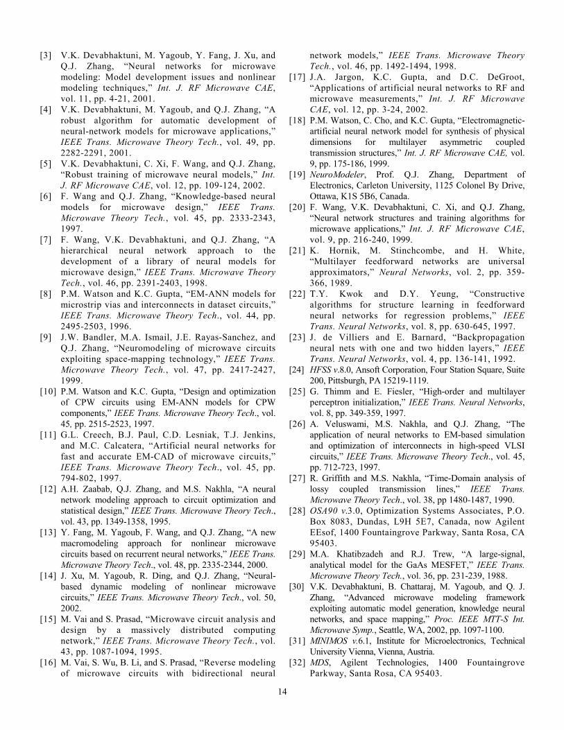
Fig. 7. Geometry of the CPW folded double-stub filter circuit. Optimization of the filter is carried out using fast EM-ANN models of various components in the circuit. voltage (Vg). Drain current (Id) is the neural model output parameter. Training and test data were generated using physics-based MINIMOS simulator [31]. The average test errors of the trained MOSFET neural models were observed to be as low as 0.50%. This fast neural model of MOSFET can therefore be used to predict the DC characteristics of the device with physics-based simulation accuracies. V. CIRCUIT OPTIMIZATION USING NEURAL NETWORK
MODELS
ANN models for RF/microwave components can be used in circuit design and optimization. To achieve this, the neural models are first incorporated into circuit simulators. For designers who run the circuit simulator, the neural models can be used in similar way as other models available in the simulators library. An ANN model can be connected with other ANN models or with any other models in the simulator to form a high-level circuit. In this section, circuit optimization examples utilizing fast and accurate neural models are presented. A. CPW Folded Double-Stub Filter In this example, a CPW folded double-stub filter shown in Figure 7 was designed. For this design, the substrate parameters (εr = 12.9, Hsub = 625 µm, tanδ = 0.0005) and the CPW parameters (W = 70 µm, G = 60 µm) were fixed, yielding Zo ≈ 50 Ω. Fast neural network models of CPW components, namely, CPW transmission line, 90° compensated bends, short-circuit stubs, and symmetric T-junctions (the one described in section IV) were trained using accurate training data from full-
L1 L2 L3 L4 R1 R2 R3 R4 C1 C2 C3 C4 Rs Vp Tr Topology
Vertices
ττττ1 ττττ2 ττττ3 ττττ4
……

wave EM simulations. Design and optimization of the fwere accomplished using HP-MDS [32] network simulatorthe EM-ANN models of various components [10]. The filter was designed for a center frequency of 26 GIdeally, the length of each short-circuit stub and the sectioline between the stubs should have a length of λ/4 at 26 GHowever, due to the presence of discontinuities, these lenneed to be adjusted. Parameters to be optimized are lstub lmid. Initial values for these lengths were determined, andcorresponding structure showed a less than ideal response wsimulated. The circuit was then optimized, using gradidescent, to provide the desired circuit response. The effecoptimization was a reduction in the two line lengthscomparison of circuit responses using the initial EM-Adesign, optimized EM-ANN design, and full-wave simulation of the optimized filter circuit are shown in FigurA good agreement was obtained between the EM-ANN full-wave EM simulations of the optimized circuit frequency range 1 - 50 GHz. B. Three-Stage MMIC Amplifier In this example, MESFET neural models were usedyield optimization of a three-stage X-band MMIC amplshown in Figure 10. Component ANN models wincorporated into circuit simulators Agilent-ADS [33] OSA90 [28]. Numerical results in this example were fromOSA90 implementation [12]. The specifications for amplifier are:
• Passband (8 - 12 GHz): 12.4 dB ≤ Gain ≤ 15.6 Input VSWR ≤ 2.8
• Stopband (less than 6 GHz and greater than 15 GGain ≤ 2 dB
The ANN models of MESFETs (developed in section IV) wused in this amplifier design. There are 14 design variables,
ERROR COMPARISON BETWEEN THE ANN MODEL AND EM SIMUPORT 1 AND THE OUTPUT POR
|S11| ∠∠∠∠ S11 |S1
Training
Average Error
Std. Deviation
0.00150
0.00128
0.754
0.696
0.00
0.00
Testing
Average Error
Std. Deviation
0.00345
0.00337
0.782
0.674
0.00
0.00
TABLE I. LATIONS FOR THE CPW SYMMETRIC T-JUNCTION. INPUT BRANCHLINE PORT IS TS ON THE MAIN LINE ARE PORTS 2 AND 3.
3| ∠∠∠∠ S13 |S23| ∠∠∠∠ S23 |S33| ∠∠∠∠ S33
071
058
0.176
0.172
0.00084
0.00097
0.246
0.237
0.00106
0.00109
0.633
0.546
11
ilter and
Hz. n of Hz. gths and the hen ent-t of . A NN EM e 9. and
over
for ifier ere and the the
dB,
Hz):
ere
Fig. 8. Comparison of small-signal S-parameter predictions from the large-signal MESFET neural network model (o, +, x, *) with those from Khatibzadeh and Trew MESFET model ( ). i.e., metal-plate areas (
iCs ) of the MIM capacitors (Ci, i = 1, 2,
3, 4) and number of turns (jLn ) of the spiral inductors (Lj, j = 1
to 10). A total of 37 statistical variables including gate length, gate width, channel thickness, and doping density of MESFET models; metal-plate area and thickness of capacitor models; and conductor width and spacing of spiral inductor models were considered. Yield optimization using l1-centering algorithm [34] was performed with minimax nominal design solution as the initial point. The initial yield (before optimization) of the amplifier using the minimax nominal design was 26% with fast ANN based simulations and 32% with relatively slow simulations using Khatibzadeh and Trew MESFET models. After yield optimization using neural network models, the amplifier yield
088
085
0.141
0.125
0.00126
0.00105
0.177
0.129
0.00083
0.00068
0.838
0.717

12
Fig. 9. Comparison of the CPW folded double-stub filter responses before and after ANN-based optimization. A good agreement is achieved between ANN-based simulations and full-wave EM simulations of the optimized circuit.
Fig. 10. A 3-stage MMIC amplifier in which the 3 MESFETs are represented by neural network models. improved from 32% to 58% as verified by the Monte-Carlo analysis using the original MESFET models. The Monte-Carlo responses before and after yield optimization are shown in Figure 11. The use of neural network models instead of
Fig. 11. Monte Carlo responses of the 3-stage MMIC amplifier. (a) & (b): Before yield optimization. (c) & (d): After yield optimization. Yield optimization was carried out using neural network models of MESFETs. Khatibzadeh and Trew models reduced the computation time for nonlinear statistical analysis and yield optimization from days to hours [12]. Considering that the Khatibzadeh and Trew models used in this example for illustration purpose are semi-analytical in nature, the CPU speed-up offered by neural based design relative to circuit design using physics-based semiconductor equations could be even more significant.
VI. CONCLUSIONS Neural networks have recently gained attention as a fast, accurate and flexible tool to RF/microwave modeling, simulation and design. As this emerging technology expands from university research into practical applications, there is a need to address the basic conceptual issues in ANN-based CAD. Through this tutorial we have tried to build a technical bridge between microwave design concepts and neural network fundamentals. Principal ideas in neural network based techniques have been explained to design-oriented readers in a simple manner. Neural network model development from beginning-to-end has been described with all the important steps involved. To demonstrate the application issues, a set of selected component modeling and circuit optimization examples have been presented. The ANN techniques are also explained through a multi-media presentation including narrative audio clips (Appendix I) in the electronic version of this article on the CD-ROM, accompanying this issue. For those readers interested in benefiting from neural networks right
-200
-150
-100
-50
0
50
100
150
200
0 10 20 30 40 50
frequency (GHz)
angl
e S 1
1 (de
gree
s)
EM-ANN Opt. EM sim. EM-ANN Org.
-50
-40
-30
-20
-10
0 0 10 20 30 40 50
frequency (GHZ)
mag
nitu
de S
11 (d
b)
Opt. EM-ANN
EM sim.
Org. EM-ANN
Vg2
Vg1 Vd2
Vg3
Input
Cg1 Cd2
Cg2 Cg3
R1 R2
C2 C4
OutputL4 L5 L6 L3 L2 L1
C1 C3
Vd3 Cd3
L7 Vd1
Cd1
L8 L9 L10

13
away, we have provided a hyperlink to NeuroModeler demonstration software (Appendix II).
APPENDIX I: MULTI-MEDIA SLIDE PRESENTATION A multi-media Microsoft PowerPoint slide presentation including narrative audio clips is made available to the readers in the form of an appendix. The presentation consisting of 55 slides provides systematic highlights of the microwave-ANN methodology and its practical applications. Some of the advanced concepts are simplified using slide-by-slide illustrations and animated transitions. The audio clips further help to make self-learning of this emerging area easier. Click PowerPoint Presentation Here to start the slide presentation.
APPENDIX II: HYPERLINK TO NEUROMODELER SOFTWARE
A hyperlink to the demonstration version of NeuroModeler software is provided. The software can be used to practice various interesting concepts in the tutorial including neural network structure creation, neural network training, neural model testing etc. The main purpose is to enable the readers to better understand the neural network based design techniques and to get a quick hands-on experience.
For illustration purpose, we show the step-by-step process of neural network training and testing in NeuroModeler using a simple example. Data Preparation:
Suppose the neural network has one input (x, say length of the metal plate of a square capacitor) and one output (y, say the normalized capacitance of the square capacitor). Suppose the test data for this illustration is
0.2 0.04 0.4 0.16 0.6 0.36 0.8 0.64 1.0 1.0
where the 1st column corresponds to x, and the 2nd column corresponds to y. There are 5 samples of (x, y) in the test data. Suppose the training (and validation) data is
0.1 0.01 0.3 0.09
0.5 0.25 0.7 0.49 0.9 0.81 1.1 1.21 where the 1st column corresponds to x, and the 2nd column corresponds to y. There are 6 samples of (x, y) in the training data. For this illustration purpose, the data was generated using a simple formula y = x2. In reality, the relationship
between x and y is more complicated, and the data should be generated from EM/physics simulation or measurement. Neural Network Training and Testing
After starting NeuroModeler, you are in the main menu. Step 1: Press <New Neural Model> and you are in the model
structure window. Select 3 Layer Perceptrons. Define the number of input neurons as 1. Define the number of output neurons as 1. The number of hidden neurons will be automatically set. Click OK to return to the main menu
Step 2: Press <Train Neural Model> and you are in the training window. Press <Get Training Data> and enter the training data. (You can copy the data from a text file and paste it into NeuroModeler data window.) Press <Start Training> and wait for the training process to finish. When training is finished, the training error curve will be plotted. You can press <Start Training> again if you want to continue to train the model further. Press <Exit> to return to the main menu.
Step 3: Press <Test Neural Model> and you are in the test window. Press <Get Test Data> and enter the test data. Press <Start Testing> to obtain the model accuracy in terms of the average test error, and worst-case test error. You can also see graphically a comparison of the trained neural network versus the test data. Press <Exit> to return to the main menu.
Step 4: If model accuracy in Step 3 is not satisfactory then go to Step 2 for further training.
Step 5: Press <Display Model Input/Output> and you are in the display window. Press <Start Simulation> to see an y=y(x) relationship estimated by your trained neural model. This should approximate the original problem represented by the training and test data. Press <Exit> to return to the main menu.
Step 6: The training and testing of the neural model are finished. Now you are welcome to try it.
Click NeuroModeler Here to start running the program.
ACKNOWLEDGEMENTS
The authors thank Larry Ton, Makarand Deo and Yi Cao of Department of Electronics at Carleton University for their help in preparing the multi-media Microsoft PowerPoint slide presentation, the manuscript and its electronic version respectively.
REFERENCES [1] Q.J. Zhang and K.C. Gupta, Neural Networks for RF and
Microwave Design, Norwood, MA: Artech House, 2000. [2] K.C. Gupta, Emerging trends in millimeter-wave
CAD, IEEE Trans. Microwave Theory Tech., vol. 46, pp. 747-755, 1998.
14
[3] V.K. Devabhaktuni, M. Yagoub, Y. Fang, J. Xu, and Q.J. Zhang, Neural networks for microwave modeling: Model development issues and nonlinear modeling techniques, Int. J. RF Microwave CAE, vol. 11, pp. 4-21, 2001.
[4] V.K. Devabhaktuni, M. Yagoub, and Q.J. Zhang, A robust algorithm for automatic development of neural-network models for microwave applications, IEEE Trans. Microwave Theory Tech., vol. 49, pp. 2282-2291, 2001.
[5] V.K. Devabhaktuni, C. Xi, F. Wang, and Q.J. Zhang, Robust training of microwave neural models, Int. J. RF Microwave CAE, vol. 12, pp. 109-124, 2002.
[6] F. Wang and Q.J. Zhang, Knowledge-based neural models for microwave design, IEEE Trans. Microwave Theory Tech., vol. 45, pp. 2333-2343, 1997.
[7] F. Wang, V.K. Devabhaktuni, and Q.J. Zhang, A hierarchical neural network approach to the development of a library of neural models for microwave design, IEEE Trans. Microwave Theory Tech., vol. 46, pp. 2391-2403, 1998.
[8] P.M. Watson and K.C. Gupta, EM-ANN models for microstrip vias and interconnects in dataset circuits, IEEE Trans. Microwave Theory Tech., vol. 44, pp. 2495-2503, 1996.
[9] J.W. Bandler, M.A. Ismail, J.E. Rayas-Sanchez, and Q.J. Zhang, Neuromodeling of microwave circuits exploiting space-mapping technology, IEEE Trans. Microwave Theory Tech., vol. 47, pp. 2417-2427, 1999.
[10] P.M. Watson and K.C. Gupta, Design and optimization of CPW circuits using EM-ANN models for CPW components, IEEE Trans. Microwave Theory Tech., vol. 45, pp. 2515-2523, 1997.
[11] G.L. Creech, B.J. Paul, C.D. Lesniak, T.J. Jenkins, and M.C. Calcatera, Artificial neural networks for fast and accurate EM-CAD of microwave circuits, IEEE Trans. Microwave Theory Tech., vol. 45, pp. 794-802, 1997.
[12] A.H. Zaabab, Q.J. Zhang, and M.S. Nakhla, A neural network modeling approach to circuit optimization and statistical design, IEEE Trans. Microwave Theory Tech., vol. 43, pp. 1349-1358, 1995.
[13] Y. Fang, M. Yagoub, F. Wang, and Q.J. Zhang, A new macromodeling approach for nonlinear microwave circuits based on recurrent neural networks, IEEE Trans. Microwave Theory Tech., vol. 48, pp. 2335-2344, 2000.
[14] J. Xu, M. Yagoub, R. Ding, and Q.J. Zhang, Neural-based dynamic modeling of nonlinear microwave circuits, IEEE Trans. Microwave Theory Tech., vol. 50, 2002.
[15] M. Vai and S. Prasad, Microwave circuit analysis and design by a massively distributed computing network, IEEE Trans. Microwave Theory Tech., vol. 43, pp. 1087-1094, 1995.
[16] M. Vai, S. Wu, B. Li, and S. Prasad, Reverse modeling of microwave circuits with bidirectional neural
network models, IEEE Trans. Microwave Theory Tech., vol. 46, pp. 1492-1494, 1998.
[17] J.A. Jargon, K.C. Gupta, and D.C. DeGroot, Applications of artificial neural networks to RF and microwave measurements, Int. J. RF Microwave CAE, vol. 12, pp. 3-24, 2002.
[18] P.M. Watson, C. Cho, and K.C. Gupta, Electromagnetic-artificial neural network model for synthesis of physical dimensions for multilayer asymmetric coupled transmission structures, Int. J. RF Microwave CAE, vol. 9, pp. 175-186, 1999.
[19] NeuroModeler, Prof. Q.J. Zhang, Department of Electronics, Carleton University, 1125 Colonel By Drive, Ottawa, K1S 5B6, Canada.
[20] F. Wang, V.K. Devabhaktuni, C. Xi, and Q.J. Zhang, Neural network structures and training algorithms for microwave applications, Int. J. RF Microwave CAE, vol. 9, pp. 216-240, 1999.
[21] K. Hornik, M. Stinchcombe, and H. White, Multilayer feedforward networks are universal approximators, Neural Networks, vol. 2, pp. 359-366, 1989.
[22] T.Y. Kwok and D.Y. Yeung, Constructive algorithms for structure learning in feedforward neural networks for regression problems, IEEE Trans. Neural Networks, vol. 8, pp. 630-645, 1997.
[23] J. de Villiers and E. Barnard, Backpropagation neural nets with one and two hidden layers, IEEE Trans. Neural Networks, vol. 4, pp. 136-141, 1992.
[24] HFSS v.8.0, Ansoft Corporation, Four Station Square, Suite 200, Pittsburgh, PA 15219-1119.
[25] G. Thimm and E. Fiesler, High-order and multilayer perceptron initialization, IEEE Trans. Neural Networks, vol. 8, pp. 349-359, 1997.
[26] A. Veluswami, M.S. Nakhla, and Q.J. Zhang, The application of neural networks to EM-based simulation and optimization of interconnects in high-speed VLSI circuits, IEEE Trans. Microwave Theory Tech., vol. 45, pp. 712-723, 1997.
[27] R. Griffith and M.S. Nakhla, Time-Domain analysis of lossy coupled transmission lines, IEEE Trans. Microwave Theory Tech., vol. 38, pp 1480-1487, 1990.
[28] OSA90 v.3.0, Optimization Systems Associates, P.O. Box 8083, Dundas, L9H 5E7, Canada, now Agilent EEsof, 1400 Fountaingrove Parkway, Santa Rosa, CA 95403.
[29] M.A. Khatibzadeh and R.J. Trew, A large-signal, analytical model for the GaAs MESFET, IEEE Trans. Microwave Theory Tech., vol. 36, pp. 231-239, 1988.
[30] V.K. Devabhaktuni, B. Chattaraj, M. Yagoub, and Q. J. Zhang, Advanced microwave modeling framework exploiting automatic model generation, knowledge neural networks, and space mapping, Proc. IEEE MTT-S Int. Microwave Symp., Seattle, WA, 2002, pp. 1097-1100.
[31] MINIMOS v.6.1, Institute for Microelectronics, Technical University Vienna, Vienna, Austria.
[32] MDS, Agilent Technologies, 1400 Fountaingrove Parkway, Santa Rosa, CA 95403.

15
[33] ADS, Agilent Technologies, 1400 Fountaingrove Parkway, Santa Rosa, CA 95403.
[34] J.W. Bandler and S.H. Chen, Circuit optimization: the state of the art, (invited), IEEE Trans. Microwave Theory Tech., vol. 36, pp. 424-443, 1988.
Qi-Jun Zhang (S84, M87, SM95) received the B.Eng. Degree from the East China Engineering Institute, Nanjing, China, in 1982, and the Ph.D. Degree in Electrical Engineering from the McMaster University, Hamilton, Canada, in 1987.
He was with the Systems Engineering Institute, Tianjin University, Tianjin, China,
during 1982-1983. From 1988 to 1990, he was with the Optimization Systems Associates Inc. (OSA), Dundas, Ontario, Canada, developing advanced microwave optimization software. He joined the Department of Electronics, Carleton University, Ottawa, Canada in 1990, where he is presently a Professor. His research interests are neural network and optimization methods for high-speed/high-frequency circuit design. He has authored and co-authored over 150 papers in the area. He is a co-author of Neural Networks for RF and Microwave Design (Artech House, Boston, 2000), a co-editor of Modeling and Simulation of High-Speed VLSI Interconnects (Kluwer, Boston, 1994), a contributor to Analog Methods for Computer-Aided Analysis and Diagnosis (Marcel Dekker, New York, 1988), a guest co-editor for a Special Issue on High-Speed VLSI Interconnects for the International Journal of Analog Integrated Circuits and Signal Processing (Kluwer, Boston, 1994), and twice a guest editor for the Special Issues on Applications of ANN to RF and Microwave Design for the International Journal of RF and Microwave CAE (Wiley, New York, 1999 and 2002). Dr. Zhang is a member of the Association of Professional Engineers of the Province of Ontario, Canada.
Kuldip C. Gupta (M62, SM74, F88) received the B.Sc. degree (Physics, Math and Chemistry) from Punjab University (India) in 1958, B.E. and M.E. degrees in Electrical Communication Engineering from the Indian Institute of Science, Bangalore, India, in 1961 an 1962, respectively, and the Ph.D. degree from the
Birla Institute of Technology and Science, Pilani, India, in 1969. Dr. Gupta has been a Professor at the University of Colorado since 1983. Presently, he is also the Associate Director for the NSF I/UCR Center for Advanced Manufacturing and Packaging of Microwave, Optical and Digital Electronics (CAMPmode) at the University of Colorado; and a Guest Researcher with RF Technology Group of National Institute of Standards and Technology (NIST) at Boulder. Earlier, he had a long stay (since 1969) at the Indian
Institute of Technology, Kanpur, where he was a Professor in Electrical Engineering until 1984. From 1971 to 1979, he was the Coordinator for the Phased Array Radar Group of the Advanced Center for Electronics Systems at the Indian Institute of Technology. On leave from IITK, he has been a Visiting Professor at the University of Waterloo, Canada; at the Ecole Polytechnique Federale de Lausanne, Switzerland; at the Technical University of Denmark (Lyngby); at the Eidgenossische Technische Hochschule, Zurich; and at the University of Kansas, Lawrence. On sabbatical from the University of Colorado in 1993-94, Dr. Gupta was a Visiting Professor at the Indian Institute of Science in Bangalore and a Consultant at the Indian Telephone Industries.
Dr. Guptas current research interests are in the area of computer-aided design techniques (including ANN applications) for microwave and millimeter-wave integrated circuits, nonlinear characterization and modeling, RF MEMS, and reconfigurable antennas. He is the author or co-author of eight books: Microwave Integrated Circuits (Wiley Eastern, 1974; Halsted Press of John Wiley, 1974); Microstrip Line and Slotlines (Artech House, 1979; revised second edition, 1996); Microwaves (Wiley Eastern, 1979; Halsted Press of John Wiley, 1980; Editorial Limusa Mexico, 1983); CAD of Microwave Circuits (Artech House, 1981; Chinese Scientific Press, 1986; Radio I Syvaz, 1987); Microstrip Antenna Design (Artech House, 1988); Analysis and Design of Planar Microwave Components (IEEE Press, 1994); Analysis and Design of Integrated Circuit-Antenna Modules (John Wiley 1999); and Neural Networks for RF and Microwave Design (Artech House 2000). Also, he has contributed chapters to the Handbook of Microstrip Antennas (Peter Peregrinus, 1989); the Handbook of Microwave and Optical Components, vol. 1 (John Wiley, 1989); Microwave Solid State Circuit Design (John Wiley, 1988; 2nd ed 2003); Numerical Techniques for Microwave and Millimeter Wave Passive Structures (John Wiley, 1989), and Encyclopedia of Electrical and Electronics Engineering (John Wiley 1999). Dr. Gupta has published over 230 research papers and holds four patents in the microwave area.
Dr. Gupta is a Fellow of the IEEE (Institute of Electrical and Electronics Engineers, USA); a Fellow of the Institution of Electronics and Telecommunication Engineers (India); a Member of URSI (Commission D, USA); and a Member of the Electromagnetics Academy (MIT, USA). He is a recipient of IEEE Third Millennium Medal and IEEE MTT-S Distinguished Educator Award. He is a member of the ADCOM for the MTT Society of IEEE, chair of the IEEE MTT-S standing committee on Education, past co-chair of the IEEE MTT-S Technical Committee on CAD (MTT-1), a member of the IEEE Technical Committee on Microwave Field Theory (MTT-15), an earlier member of IEEE-EAB Committee on Continuing Education, and of IEEE-EAB Societies Education Committee. He is the founding editor of the International Journal of RF and Microwave Computer-Aided Engineering, published by John Wiley since 1991. He is an Associate Editor for IEEE Microwave Magazine, on the editorial boards of IEEE Transactions on Microwave Theory and Techniques, Microwave and Optical Technology Letters (John Wiley), and
16
International Journal of Numerical Modeling (John Wiley, U.K.). He is listed in Whos Who in America, Whos Who in the World, Whos Who in Engineering, and Whos Who in American Education.
Vijay K. Devabhaktuni (S97) received the B.Eng. degree in Electrical and Electronics and the M.Sc. degree in Physics, both from the Birla Institute of Technology and Science, Pilani, Rajasthan, India, in 1996. He is currently a Ph.D. Candidate and Sessional Lecturer in the Department of Electronics, Carleton
University, Ottawa, Canada. He is the winner of a best student research exhibit award from Nortel Networks in 1999. He is a two-time recipient of the Ontario Graduate Scholarship for the academic years 1999-2000 and 2000-2001, from the Ministry of Education and Training, Ontario, Canada. He received the John Ruptash Memorial Fellowship awarded annually to an outstanding graduate student in the Faculty of Engineering at Carleton University for the year 2001. He also received the Teaching Excellence Award in Engineering from the Carleton University Students Association in 2001. His research interests include artificial neural networks, computer-aided design methodologies for VLSI circuits, and RF and microwave modeling techniques.